JP3669809B2 - Gold alloy wire for semiconductor element bonding - Google Patents
Gold alloy wire for semiconductor element bonding Download PDFInfo
- Publication number
- JP3669809B2 JP3669809B2 JP10896197A JP10896197A JP3669809B2 JP 3669809 B2 JP3669809 B2 JP 3669809B2 JP 10896197 A JP10896197 A JP 10896197A JP 10896197 A JP10896197 A JP 10896197A JP 3669809 B2 JP3669809 B2 JP 3669809B2
- Authority
- JP
- Japan
- Prior art keywords
- ppm
- weight
- alloy wire
- gold
- predetermined amount
- Prior art date
- Legal status (The legal status is an assumption and is not a legal conclusion. Google has not performed a legal analysis and makes no representation as to the accuracy of the status listed.)
- Expired - Fee Related
Links
Images

Classifications
-
- C—CHEMISTRY; METALLURGY
- C22—METALLURGY; FERROUS OR NON-FERROUS ALLOYS; TREATMENT OF ALLOYS OR NON-FERROUS METALS
- C22C—ALLOYS
- C22C5/00—Alloys based on noble metals
- C22C5/02—Alloys based on gold
-
- B—PERFORMING OPERATIONS; TRANSPORTING
- B23—MACHINE TOOLS; METAL-WORKING NOT OTHERWISE PROVIDED FOR
- B23K—SOLDERING OR UNSOLDERING; WELDING; CLADDING OR PLATING BY SOLDERING OR WELDING; CUTTING BY APPLYING HEAT LOCALLY, e.g. FLAME CUTTING; WORKING BY LASER BEAM
- B23K35/00—Rods, electrodes, materials, or media, for use in soldering, welding, or cutting
- B23K35/22—Rods, electrodes, materials, or media, for use in soldering, welding, or cutting characterised by the composition or nature of the material
- B23K35/24—Selection of soldering or welding materials proper
- B23K35/30—Selection of soldering or welding materials proper with the principal constituent melting at less than 1550 degrees C
- B23K35/3013—Au as the principal constituent
-
- H—ELECTRICITY
- H01—ELECTRIC ELEMENTS
- H01L—SEMICONDUCTOR DEVICES NOT COVERED BY CLASS H10
- H01L2224/00—Indexing scheme for arrangements for connecting or disconnecting semiconductor or solid-state bodies and methods related thereto as covered by H01L24/00
- H01L2224/01—Means for bonding being attached to, or being formed on, the surface to be connected, e.g. chip-to-package, die-attach, "first-level" interconnects; Manufacturing methods related thereto
- H01L2224/02—Bonding areas; Manufacturing methods related thereto
- H01L2224/04—Structure, shape, material or disposition of the bonding areas prior to the connecting process
- H01L2224/05—Structure, shape, material or disposition of the bonding areas prior to the connecting process of an individual bonding area
- H01L2224/0554—External layer
- H01L2224/05599—Material
- H01L2224/056—Material with a principal constituent of the material being a metal or a metalloid, e.g. boron [B], silicon [Si], germanium [Ge], arsenic [As], antimony [Sb], tellurium [Te] and polonium [Po], and alloys thereof
- H01L2224/05617—Material with a principal constituent of the material being a metal or a metalloid, e.g. boron [B], silicon [Si], germanium [Ge], arsenic [As], antimony [Sb], tellurium [Te] and polonium [Po], and alloys thereof the principal constituent melting at a temperature of greater than or equal to 400°C and less than 950°C
- H01L2224/05624—Aluminium [Al] as principal constituent
-
- H—ELECTRICITY
- H01—ELECTRIC ELEMENTS
- H01L—SEMICONDUCTOR DEVICES NOT COVERED BY CLASS H10
- H01L2224/00—Indexing scheme for arrangements for connecting or disconnecting semiconductor or solid-state bodies and methods related thereto as covered by H01L24/00
- H01L2224/01—Means for bonding being attached to, or being formed on, the surface to be connected, e.g. chip-to-package, die-attach, "first-level" interconnects; Manufacturing methods related thereto
- H01L2224/42—Wire connectors; Manufacturing methods related thereto
- H01L2224/43—Manufacturing methods
-
- H—ELECTRICITY
- H01—ELECTRIC ELEMENTS
- H01L—SEMICONDUCTOR DEVICES NOT COVERED BY CLASS H10
- H01L2224/00—Indexing scheme for arrangements for connecting or disconnecting semiconductor or solid-state bodies and methods related thereto as covered by H01L24/00
- H01L2224/01—Means for bonding being attached to, or being formed on, the surface to be connected, e.g. chip-to-package, die-attach, "first-level" interconnects; Manufacturing methods related thereto
- H01L2224/42—Wire connectors; Manufacturing methods related thereto
- H01L2224/44—Structure, shape, material or disposition of the wire connectors prior to the connecting process
- H01L2224/45—Structure, shape, material or disposition of the wire connectors prior to the connecting process of an individual wire connector
- H01L2224/45001—Core members of the connector
- H01L2224/4501—Shape
- H01L2224/45012—Cross-sectional shape
- H01L2224/45015—Cross-sectional shape being circular
-
- H—ELECTRICITY
- H01—ELECTRIC ELEMENTS
- H01L—SEMICONDUCTOR DEVICES NOT COVERED BY CLASS H10
- H01L2224/00—Indexing scheme for arrangements for connecting or disconnecting semiconductor or solid-state bodies and methods related thereto as covered by H01L24/00
- H01L2224/01—Means for bonding being attached to, or being formed on, the surface to be connected, e.g. chip-to-package, die-attach, "first-level" interconnects; Manufacturing methods related thereto
- H01L2224/42—Wire connectors; Manufacturing methods related thereto
- H01L2224/44—Structure, shape, material or disposition of the wire connectors prior to the connecting process
- H01L2224/45—Structure, shape, material or disposition of the wire connectors prior to the connecting process of an individual wire connector
- H01L2224/45001—Core members of the connector
- H01L2224/45099—Material
- H01L2224/451—Material with a principal constituent of the material being a metal or a metalloid, e.g. boron (B), silicon (Si), germanium (Ge), arsenic (As), antimony (Sb), tellurium (Te) and polonium (Po), and alloys thereof
- H01L2224/45138—Material with a principal constituent of the material being a metal or a metalloid, e.g. boron (B), silicon (Si), germanium (Ge), arsenic (As), antimony (Sb), tellurium (Te) and polonium (Po), and alloys thereof the principal constituent melting at a temperature of greater than or equal to 950°C and less than 1550°C
- H01L2224/45144—Gold (Au) as principal constituent
-
- H—ELECTRICITY
- H01—ELECTRIC ELEMENTS
- H01L—SEMICONDUCTOR DEVICES NOT COVERED BY CLASS H10
- H01L2224/00—Indexing scheme for arrangements for connecting or disconnecting semiconductor or solid-state bodies and methods related thereto as covered by H01L24/00
- H01L2224/01—Means for bonding being attached to, or being formed on, the surface to be connected, e.g. chip-to-package, die-attach, "first-level" interconnects; Manufacturing methods related thereto
- H01L2224/42—Wire connectors; Manufacturing methods related thereto
- H01L2224/47—Structure, shape, material or disposition of the wire connectors after the connecting process
- H01L2224/48—Structure, shape, material or disposition of the wire connectors after the connecting process of an individual wire connector
- H01L2224/4805—Shape
- H01L2224/4809—Loop shape
- H01L2224/48091—Arched
-
- H—ELECTRICITY
- H01—ELECTRIC ELEMENTS
- H01L—SEMICONDUCTOR DEVICES NOT COVERED BY CLASS H10
- H01L2224/00—Indexing scheme for arrangements for connecting or disconnecting semiconductor or solid-state bodies and methods related thereto as covered by H01L24/00
- H01L2224/01—Means for bonding being attached to, or being formed on, the surface to be connected, e.g. chip-to-package, die-attach, "first-level" interconnects; Manufacturing methods related thereto
- H01L2224/42—Wire connectors; Manufacturing methods related thereto
- H01L2224/47—Structure, shape, material or disposition of the wire connectors after the connecting process
- H01L2224/48—Structure, shape, material or disposition of the wire connectors after the connecting process of an individual wire connector
- H01L2224/481—Disposition
- H01L2224/48151—Connecting between a semiconductor or solid-state body and an item not being a semiconductor or solid-state body, e.g. chip-to-substrate, chip-to-passive
- H01L2224/48221—Connecting between a semiconductor or solid-state body and an item not being a semiconductor or solid-state body, e.g. chip-to-substrate, chip-to-passive the body and the item being stacked
- H01L2224/48245—Connecting between a semiconductor or solid-state body and an item not being a semiconductor or solid-state body, e.g. chip-to-substrate, chip-to-passive the body and the item being stacked the item being metallic
- H01L2224/48247—Connecting between a semiconductor or solid-state body and an item not being a semiconductor or solid-state body, e.g. chip-to-substrate, chip-to-passive the body and the item being stacked the item being metallic connecting the wire to a bond pad of the item
-
- H—ELECTRICITY
- H01—ELECTRIC ELEMENTS
- H01L—SEMICONDUCTOR DEVICES NOT COVERED BY CLASS H10
- H01L2224/00—Indexing scheme for arrangements for connecting or disconnecting semiconductor or solid-state bodies and methods related thereto as covered by H01L24/00
- H01L2224/01—Means for bonding being attached to, or being formed on, the surface to be connected, e.g. chip-to-package, die-attach, "first-level" interconnects; Manufacturing methods related thereto
- H01L2224/42—Wire connectors; Manufacturing methods related thereto
- H01L2224/47—Structure, shape, material or disposition of the wire connectors after the connecting process
- H01L2224/48—Structure, shape, material or disposition of the wire connectors after the connecting process of an individual wire connector
- H01L2224/484—Connecting portions
- H01L2224/48463—Connecting portions the connecting portion on the bonding area of the semiconductor or solid-state body being a ball bond
- H01L2224/48465—Connecting portions the connecting portion on the bonding area of the semiconductor or solid-state body being a ball bond the other connecting portion not on the bonding area being a wedge bond, i.e. ball-to-wedge, regular stitch
-
- H—ELECTRICITY
- H01—ELECTRIC ELEMENTS
- H01L—SEMICONDUCTOR DEVICES NOT COVERED BY CLASS H10
- H01L2224/00—Indexing scheme for arrangements for connecting or disconnecting semiconductor or solid-state bodies and methods related thereto as covered by H01L24/00
- H01L2224/01—Means for bonding being attached to, or being formed on, the surface to be connected, e.g. chip-to-package, die-attach, "first-level" interconnects; Manufacturing methods related thereto
- H01L2224/42—Wire connectors; Manufacturing methods related thereto
- H01L2224/47—Structure, shape, material or disposition of the wire connectors after the connecting process
- H01L2224/48—Structure, shape, material or disposition of the wire connectors after the connecting process of an individual wire connector
- H01L2224/485—Material
- H01L2224/48505—Material at the bonding interface
- H01L2224/48599—Principal constituent of the connecting portion of the wire connector being Gold (Au)
- H01L2224/486—Principal constituent of the connecting portion of the wire connector being Gold (Au) with a principal constituent of the bonding area being a metal or a metalloid, e.g. boron (B), silicon (Si), germanium (Ge), arsenic (As), antimony (Sb), tellurium (Te) and polonium (Po), and alloys thereof
- H01L2224/48617—Principal constituent of the connecting portion of the wire connector being Gold (Au) with a principal constituent of the bonding area being a metal or a metalloid, e.g. boron (B), silicon (Si), germanium (Ge), arsenic (As), antimony (Sb), tellurium (Te) and polonium (Po), and alloys thereof the principal constituent melting at a temperature of greater than or equal to 400°C and less than 950 °C
- H01L2224/48624—Aluminium (Al) as principal constituent
-
- H—ELECTRICITY
- H01—ELECTRIC ELEMENTS
- H01L—SEMICONDUCTOR DEVICES NOT COVERED BY CLASS H10
- H01L2224/00—Indexing scheme for arrangements for connecting or disconnecting semiconductor or solid-state bodies and methods related thereto as covered by H01L24/00
- H01L2224/74—Apparatus for manufacturing arrangements for connecting or disconnecting semiconductor or solid-state bodies and for methods related thereto
- H01L2224/78—Apparatus for connecting with wire connectors
- H01L2224/787—Means for aligning
- H01L2224/78701—Means for aligning in the lower part of the bonding apparatus, e.g. in the apparatus chuck
-
- H—ELECTRICITY
- H01—ELECTRIC ELEMENTS
- H01L—SEMICONDUCTOR DEVICES NOT COVERED BY CLASS H10
- H01L2224/00—Indexing scheme for arrangements for connecting or disconnecting semiconductor or solid-state bodies and methods related thereto as covered by H01L24/00
- H01L2224/74—Apparatus for manufacturing arrangements for connecting or disconnecting semiconductor or solid-state bodies and for methods related thereto
- H01L2224/78—Apparatus for connecting with wire connectors
- H01L2224/787—Means for aligning
- H01L2224/78703—Mechanical holding means
-
- H—ELECTRICITY
- H01—ELECTRIC ELEMENTS
- H01L—SEMICONDUCTOR DEVICES NOT COVERED BY CLASS H10
- H01L2924/00—Indexing scheme for arrangements or methods for connecting or disconnecting semiconductor or solid-state bodies as covered by H01L24/00
- H01L2924/0001—Technical content checked by a classifier
- H01L2924/00011—Not relevant to the scope of the group, the symbol of which is combined with the symbol of this group
-
- H—ELECTRICITY
- H01—ELECTRIC ELEMENTS
- H01L—SEMICONDUCTOR DEVICES NOT COVERED BY CLASS H10
- H01L2924/00—Indexing scheme for arrangements or methods for connecting or disconnecting semiconductor or solid-state bodies as covered by H01L24/00
- H01L2924/01—Chemical elements
- H01L2924/01004—Beryllium [Be]
-
- H—ELECTRICITY
- H01—ELECTRIC ELEMENTS
- H01L—SEMICONDUCTOR DEVICES NOT COVERED BY CLASS H10
- H01L2924/00—Indexing scheme for arrangements or methods for connecting or disconnecting semiconductor or solid-state bodies as covered by H01L24/00
- H01L2924/01—Chemical elements
- H01L2924/01006—Carbon [C]
-
- H—ELECTRICITY
- H01—ELECTRIC ELEMENTS
- H01L—SEMICONDUCTOR DEVICES NOT COVERED BY CLASS H10
- H01L2924/00—Indexing scheme for arrangements or methods for connecting or disconnecting semiconductor or solid-state bodies as covered by H01L24/00
- H01L2924/01—Chemical elements
- H01L2924/01013—Aluminum [Al]
-
- H—ELECTRICITY
- H01—ELECTRIC ELEMENTS
- H01L—SEMICONDUCTOR DEVICES NOT COVERED BY CLASS H10
- H01L2924/00—Indexing scheme for arrangements or methods for connecting or disconnecting semiconductor or solid-state bodies as covered by H01L24/00
- H01L2924/01—Chemical elements
- H01L2924/01019—Potassium [K]
-
- H—ELECTRICITY
- H01—ELECTRIC ELEMENTS
- H01L—SEMICONDUCTOR DEVICES NOT COVERED BY CLASS H10
- H01L2924/00—Indexing scheme for arrangements or methods for connecting or disconnecting semiconductor or solid-state bodies as covered by H01L24/00
- H01L2924/01—Chemical elements
- H01L2924/0102—Calcium [Ca]
-
- H—ELECTRICITY
- H01—ELECTRIC ELEMENTS
- H01L—SEMICONDUCTOR DEVICES NOT COVERED BY CLASS H10
- H01L2924/00—Indexing scheme for arrangements or methods for connecting or disconnecting semiconductor or solid-state bodies as covered by H01L24/00
- H01L2924/01—Chemical elements
- H01L2924/01029—Copper [Cu]
-
- H—ELECTRICITY
- H01—ELECTRIC ELEMENTS
- H01L—SEMICONDUCTOR DEVICES NOT COVERED BY CLASS H10
- H01L2924/00—Indexing scheme for arrangements or methods for connecting or disconnecting semiconductor or solid-state bodies as covered by H01L24/00
- H01L2924/01—Chemical elements
- H01L2924/01033—Arsenic [As]
-
- H—ELECTRICITY
- H01—ELECTRIC ELEMENTS
- H01L—SEMICONDUCTOR DEVICES NOT COVERED BY CLASS H10
- H01L2924/00—Indexing scheme for arrangements or methods for connecting or disconnecting semiconductor or solid-state bodies as covered by H01L24/00
- H01L2924/01—Chemical elements
- H01L2924/01037—Rubidium [Rb]
-
- H—ELECTRICITY
- H01—ELECTRIC ELEMENTS
- H01L—SEMICONDUCTOR DEVICES NOT COVERED BY CLASS H10
- H01L2924/00—Indexing scheme for arrangements or methods for connecting or disconnecting semiconductor or solid-state bodies as covered by H01L24/00
- H01L2924/01—Chemical elements
- H01L2924/01044—Ruthenium [Ru]
-
- H—ELECTRICITY
- H01—ELECTRIC ELEMENTS
- H01L—SEMICONDUCTOR DEVICES NOT COVERED BY CLASS H10
- H01L2924/00—Indexing scheme for arrangements or methods for connecting or disconnecting semiconductor or solid-state bodies as covered by H01L24/00
- H01L2924/01—Chemical elements
- H01L2924/01045—Rhodium [Rh]
-
- H—ELECTRICITY
- H01—ELECTRIC ELEMENTS
- H01L—SEMICONDUCTOR DEVICES NOT COVERED BY CLASS H10
- H01L2924/00—Indexing scheme for arrangements or methods for connecting or disconnecting semiconductor or solid-state bodies as covered by H01L24/00
- H01L2924/01—Chemical elements
- H01L2924/01046—Palladium [Pd]
-
- H—ELECTRICITY
- H01—ELECTRIC ELEMENTS
- H01L—SEMICONDUCTOR DEVICES NOT COVERED BY CLASS H10
- H01L2924/00—Indexing scheme for arrangements or methods for connecting or disconnecting semiconductor or solid-state bodies as covered by H01L24/00
- H01L2924/01—Chemical elements
- H01L2924/01047—Silver [Ag]
-
- H—ELECTRICITY
- H01—ELECTRIC ELEMENTS
- H01L—SEMICONDUCTOR DEVICES NOT COVERED BY CLASS H10
- H01L2924/00—Indexing scheme for arrangements or methods for connecting or disconnecting semiconductor or solid-state bodies as covered by H01L24/00
- H01L2924/01—Chemical elements
- H01L2924/01049—Indium [In]
-
- H—ELECTRICITY
- H01—ELECTRIC ELEMENTS
- H01L—SEMICONDUCTOR DEVICES NOT COVERED BY CLASS H10
- H01L2924/00—Indexing scheme for arrangements or methods for connecting or disconnecting semiconductor or solid-state bodies as covered by H01L24/00
- H01L2924/01—Chemical elements
- H01L2924/0105—Tin [Sn]
-
- H—ELECTRICITY
- H01—ELECTRIC ELEMENTS
- H01L—SEMICONDUCTOR DEVICES NOT COVERED BY CLASS H10
- H01L2924/00—Indexing scheme for arrangements or methods for connecting or disconnecting semiconductor or solid-state bodies as covered by H01L24/00
- H01L2924/01—Chemical elements
- H01L2924/01057—Lanthanum [La]
-
- H—ELECTRICITY
- H01—ELECTRIC ELEMENTS
- H01L—SEMICONDUCTOR DEVICES NOT COVERED BY CLASS H10
- H01L2924/00—Indexing scheme for arrangements or methods for connecting or disconnecting semiconductor or solid-state bodies as covered by H01L24/00
- H01L2924/01—Chemical elements
- H01L2924/01058—Cerium [Ce]
-
- H—ELECTRICITY
- H01—ELECTRIC ELEMENTS
- H01L—SEMICONDUCTOR DEVICES NOT COVERED BY CLASS H10
- H01L2924/00—Indexing scheme for arrangements or methods for connecting or disconnecting semiconductor or solid-state bodies as covered by H01L24/00
- H01L2924/01—Chemical elements
- H01L2924/01063—Europium [Eu]
-
- H—ELECTRICITY
- H01—ELECTRIC ELEMENTS
- H01L—SEMICONDUCTOR DEVICES NOT COVERED BY CLASS H10
- H01L2924/00—Indexing scheme for arrangements or methods for connecting or disconnecting semiconductor or solid-state bodies as covered by H01L24/00
- H01L2924/01—Chemical elements
- H01L2924/0107—Ytterbium [Yb]
-
- H—ELECTRICITY
- H01—ELECTRIC ELEMENTS
- H01L—SEMICONDUCTOR DEVICES NOT COVERED BY CLASS H10
- H01L2924/00—Indexing scheme for arrangements or methods for connecting or disconnecting semiconductor or solid-state bodies as covered by H01L24/00
- H01L2924/01—Chemical elements
- H01L2924/01076—Osmium [Os]
-
- H—ELECTRICITY
- H01—ELECTRIC ELEMENTS
- H01L—SEMICONDUCTOR DEVICES NOT COVERED BY CLASS H10
- H01L2924/00—Indexing scheme for arrangements or methods for connecting or disconnecting semiconductor or solid-state bodies as covered by H01L24/00
- H01L2924/01—Chemical elements
- H01L2924/01077—Iridium [Ir]
-
- H—ELECTRICITY
- H01—ELECTRIC ELEMENTS
- H01L—SEMICONDUCTOR DEVICES NOT COVERED BY CLASS H10
- H01L2924/00—Indexing scheme for arrangements or methods for connecting or disconnecting semiconductor or solid-state bodies as covered by H01L24/00
- H01L2924/01—Chemical elements
- H01L2924/01078—Platinum [Pt]
-
- H—ELECTRICITY
- H01—ELECTRIC ELEMENTS
- H01L—SEMICONDUCTOR DEVICES NOT COVERED BY CLASS H10
- H01L2924/00—Indexing scheme for arrangements or methods for connecting or disconnecting semiconductor or solid-state bodies as covered by H01L24/00
- H01L2924/01—Chemical elements
- H01L2924/01079—Gold [Au]
-
- H—ELECTRICITY
- H01—ELECTRIC ELEMENTS
- H01L—SEMICONDUCTOR DEVICES NOT COVERED BY CLASS H10
- H01L2924/00—Indexing scheme for arrangements or methods for connecting or disconnecting semiconductor or solid-state bodies as covered by H01L24/00
- H01L2924/01—Chemical elements
- H01L2924/01082—Lead [Pb]
-
- H—ELECTRICITY
- H01—ELECTRIC ELEMENTS
- H01L—SEMICONDUCTOR DEVICES NOT COVERED BY CLASS H10
- H01L2924/00—Indexing scheme for arrangements or methods for connecting or disconnecting semiconductor or solid-state bodies as covered by H01L24/00
- H01L2924/011—Groups of the periodic table
- H01L2924/01105—Rare earth metals
-
- H—ELECTRICITY
- H01—ELECTRIC ELEMENTS
- H01L—SEMICONDUCTOR DEVICES NOT COVERED BY CLASS H10
- H01L2924/00—Indexing scheme for arrangements or methods for connecting or disconnecting semiconductor or solid-state bodies as covered by H01L24/00
- H01L2924/10—Details of semiconductor or other solid state devices to be connected
- H01L2924/11—Device type
- H01L2924/14—Integrated circuits
-
- H—ELECTRICITY
- H01—ELECTRIC ELEMENTS
- H01L—SEMICONDUCTOR DEVICES NOT COVERED BY CLASS H10
- H01L2924/00—Indexing scheme for arrangements or methods for connecting or disconnecting semiconductor or solid-state bodies as covered by H01L24/00
- H01L2924/15—Details of package parts other than the semiconductor or other solid state devices to be connected
- H01L2924/151—Die mounting substrate
- H01L2924/156—Material
- H01L2924/157—Material with a principal constituent of the material being a metal or a metalloid, e.g. boron [B], silicon [Si], germanium [Ge], arsenic [As], antimony [Sb], tellurium [Te] and polonium [Po], and alloys thereof
- H01L2924/15738—Material with a principal constituent of the material being a metal or a metalloid, e.g. boron [B], silicon [Si], germanium [Ge], arsenic [As], antimony [Sb], tellurium [Te] and polonium [Po], and alloys thereof the principal constituent melting at a temperature of greater than or equal to 950 C and less than 1550 C
- H01L2924/15747—Copper [Cu] as principal constituent
-
- H—ELECTRICITY
- H01—ELECTRIC ELEMENTS
- H01L—SEMICONDUCTOR DEVICES NOT COVERED BY CLASS H10
- H01L2924/00—Indexing scheme for arrangements or methods for connecting or disconnecting semiconductor or solid-state bodies as covered by H01L24/00
- H01L2924/20—Parameters
- H01L2924/207—Diameter ranges
- H01L2924/20751—Diameter ranges larger or equal to 10 microns less than 20 microns
-
- H—ELECTRICITY
- H01—ELECTRIC ELEMENTS
- H01L—SEMICONDUCTOR DEVICES NOT COVERED BY CLASS H10
- H01L2924/00—Indexing scheme for arrangements or methods for connecting or disconnecting semiconductor or solid-state bodies as covered by H01L24/00
- H01L2924/20—Parameters
- H01L2924/207—Diameter ranges
- H01L2924/20752—Diameter ranges larger or equal to 20 microns less than 30 microns
-
- H—ELECTRICITY
- H01—ELECTRIC ELEMENTS
- H01L—SEMICONDUCTOR DEVICES NOT COVERED BY CLASS H10
- H01L2924/00—Indexing scheme for arrangements or methods for connecting or disconnecting semiconductor or solid-state bodies as covered by H01L24/00
- H01L2924/20—Parameters
- H01L2924/207—Diameter ranges
- H01L2924/20753—Diameter ranges larger or equal to 30 microns less than 40 microns
-
- H—ELECTRICITY
- H01—ELECTRIC ELEMENTS
- H01L—SEMICONDUCTOR DEVICES NOT COVERED BY CLASS H10
- H01L2924/00—Indexing scheme for arrangements or methods for connecting or disconnecting semiconductor or solid-state bodies as covered by H01L24/00
- H01L2924/20—Parameters
- H01L2924/207—Diameter ranges
- H01L2924/20754—Diameter ranges larger or equal to 40 microns less than 50 microns
-
- H—ELECTRICITY
- H01—ELECTRIC ELEMENTS
- H01L—SEMICONDUCTOR DEVICES NOT COVERED BY CLASS H10
- H01L2924/00—Indexing scheme for arrangements or methods for connecting or disconnecting semiconductor or solid-state bodies as covered by H01L24/00
- H01L2924/20—Parameters
- H01L2924/207—Diameter ranges
- H01L2924/20755—Diameter ranges larger or equal to 50 microns less than 60 microns
-
- H—ELECTRICITY
- H01—ELECTRIC ELEMENTS
- H01L—SEMICONDUCTOR DEVICES NOT COVERED BY CLASS H10
- H01L2924/00—Indexing scheme for arrangements or methods for connecting or disconnecting semiconductor or solid-state bodies as covered by H01L24/00
- H01L2924/20—Parameters
- H01L2924/207—Diameter ranges
- H01L2924/20756—Diameter ranges larger or equal to 60 microns less than 70 microns
-
- H—ELECTRICITY
- H01—ELECTRIC ELEMENTS
- H01L—SEMICONDUCTOR DEVICES NOT COVERED BY CLASS H10
- H01L2924/00—Indexing scheme for arrangements or methods for connecting or disconnecting semiconductor or solid-state bodies as covered by H01L24/00
- H01L2924/20—Parameters
- H01L2924/207—Diameter ranges
- H01L2924/20757—Diameter ranges larger or equal to 70 microns less than 80 microns
-
- H—ELECTRICITY
- H01—ELECTRIC ELEMENTS
- H01L—SEMICONDUCTOR DEVICES NOT COVERED BY CLASS H10
- H01L2924/00—Indexing scheme for arrangements or methods for connecting or disconnecting semiconductor or solid-state bodies as covered by H01L24/00
- H01L2924/20—Parameters
- H01L2924/207—Diameter ranges
- H01L2924/20758—Diameter ranges larger or equal to 80 microns less than 90 microns
-
- H—ELECTRICITY
- H01—ELECTRIC ELEMENTS
- H01L—SEMICONDUCTOR DEVICES NOT COVERED BY CLASS H10
- H01L2924/00—Indexing scheme for arrangements or methods for connecting or disconnecting semiconductor or solid-state bodies as covered by H01L24/00
- H01L2924/20—Parameters
- H01L2924/207—Diameter ranges
- H01L2924/20759—Diameter ranges larger or equal to 90 microns less than 100 microns
-
- H—ELECTRICITY
- H01—ELECTRIC ELEMENTS
- H01L—SEMICONDUCTOR DEVICES NOT COVERED BY CLASS H10
- H01L2924/00—Indexing scheme for arrangements or methods for connecting or disconnecting semiconductor or solid-state bodies as covered by H01L24/00
- H01L2924/20—Parameters
- H01L2924/207—Diameter ranges
- H01L2924/2076—Diameter ranges equal to or larger than 100 microns
Landscapes
- Engineering & Computer Science (AREA)
- Mechanical Engineering (AREA)
- Chemical & Material Sciences (AREA)
- Materials Engineering (AREA)
- Metallurgy (AREA)
- Organic Chemistry (AREA)
- Wire Bonding (AREA)
Abstract
Description
【0001】
【発明の属する技術分野】
本発明は、半導体素子の電極と外部リード部を接続するために使用するボンディング用金合金線に関する。
【0002】
【従来の技術】
従来からトランジスタ、IC,LSI等の半導体素子の電極と外部リードを接続する技術としては、純度99.99重量%以上の高純度金に他の金属元素を微量含有させた金合金線を用いて配線する超音波併用熱圧着ボンディング法が主として用いられている。
【0003】
ここで超音波併用熱圧着ボンディング法により配線し、ループを形成した状態を図1に示す。1はICチップ、2はICチップ上のAl電極、3は金合金線、4はリードフレーム、5はファースト側接合点、6はセカンド側接合点である。最近半導体装置は外部リード材料として放熱性、コストを考慮して銅合金製のリードフレームを用いる事が多くなってきた。銅合金製のリードフレームを用いた場合、封止用樹脂とリードフレームの熱膨張係数の差が大きく、半導体装置の作動による温度上昇によってループを形成した金合金線に外部応力が加わり、とりわけ半導体装置が過酷な熱サイクルの環境に晒された場合、断線を生じ易くなるという問題がある。
【0004】
また半導体装置の小型化、高密度化の要求が高まる中で、ICチップの多ピン化及びこれに伴う狭ピッチ化が要求されている。多ピン化、狭ピッチ化を達成する為には、ループ形状が安定している事が必要である。一方超音波併用熱圧着ボンディング法で配線を行う際、リードフレーム下部に設置された熱源により150〜250℃で加熱されている。この時加熱温度が高いと接着性は良いものの、リードフレームのそりが生じ易くなりループ形状にばらつきが生じ易くなる。また加熱温度が低いとループ形状は安定するものの低温接合であるため、金合金線とリードフレームの接合点(以下セカンド側接合点という)での接合性に問題が生じてくる。この為ループ形状にばらつきが生じることを抑制する為にボンディング時の加熱温度を150℃と低温度で行いながらセカンド側接合点での接合性に優れた金合金線が要求されている。
【0005】
従来から提案されている金合金線として特開平3−257129号公報には所定量のLa,Ca,Sn等を金に含有させることによりループ変形に効果のあることが提案されている。また特開平8−291348号公報には所定量のLa,Ca,In等を金に含有させることにより接合強度に効果のあることが提案されている。
【0006】
【発明が解決しようとする課題】
しかしながら前記提案においては、前述の要求に対して未だ不十分である。
本発明は上述したような事情に鑑みてなされたものであり、その目的とするところは、銅合金製のリードフレームを用いた半導体装置が過酷な熱サイクルの環境に晒された場合でも、断線を抑制する効果が向上すること、及びボンディング時のループ形状を安定させる為に、ボンディング時の加熱温度を150℃と低温度で行いながらセカンド側接合点での接合性、とりわけピール強度及び振動破断性能が向上した金合金線を提供することである。
【0007】
【課題を解決するための手段】
本発明者等が鋭意研究を重ねた結果、所定量のInとSnとLa,Ce,Eu,Ybのうち少なくとも1種とAg,Pt,Pd,Rh,Ir,Os,Ruのうち少なくとも1種、及び残部が金と不可避不純物からなる組成の金合金線とすることにより、前述の目的を達成し得ることを知見し、本発明を完成するに至った。
【0008】
すなわち、本発明は下記にある。
(1)インジウム(In)を1〜50重量ppm 、錫(Sn)を1〜50重量ppm 、La,Ce,Eu,Ybのうち少なくとも1種を1〜50重量ppm 、Ag,Pt,Pd,Rh,Ir,Os,Ruのうち少なくとも1種を1〜100重量ppm 、及び残部が金及び不可避不純物からなることを特徴とする半導体素子ボンディング用金合金線。
(2)さらにCa,Ge,Beのうち少なくとも1種を50重量ppm 以下添加したことを特徴とする請求項1記載の半導体素子ボンディング用金合金線。
(3)La,Ce,Eu,Ybのうち少なくとも1種がLaであることを特徴とする請求項1、請求項2記載の半導体素子ボンディング用金合金線。
(4)Ag,Pt,Pd,Rh,Ir,Os,Ruのうち少なくとも1種の含有量が9〜100重量ppm であることを特徴とする請求項3記載の半導体素子ボンディング用金合金線。
【0009】
【発明の実施の形態】
原料金としては少なくとも99.99重量%以上に精製した高純度金を用いることが好ましい。更に好ましくは99.995重量%以上であり、最も好ましくは99.999重量%以上である。この為合金中の不可避不純物は0.01重量%以下が好ましい。更に好ましくは0.005重量%以下であり、最も好ましくは0.001重量%以下である。
【0010】
高純度金に所定量のSnと所定量のLa,Ce,Eu,Ybのうち少なくとも1種と所定量のAg,Pt,Pd,Rh,Ir,Os,Ruのうち少なくとも1種との共存において、所定量のInを含有した組成とすることにより、前記課題を達成することが出来る。
この共存組成においてInの含有量が1重量ppm 以上になると、1重量ppm 未満のものと対比してセカンド側の接合性が向上してくる。即ちピール強度が大きくなり、振動破断性能が向上してくる。また熱サイクル後の断線性能も向上してくる。Inの含有量が50重量ppm を超えると、セカンド側の接合性と熱サイクル後の断線性能がともに低下してくる。この為前記共存組成におけるInの含有量を1〜50重量ppm と定めた。
【0011】
高純度金に所定量のInと所定量のLa,Ce,Eu,Ybのうち少なくとも1種と所定量のAg,Pt,Pd,Rh,Ir,Os,Ruのうち少なくとも1種との共存において、所定量のSnを含有した組成とすることにより、前記課題を達成することが出来る。
この共存組成においてSnの含有量が1重量ppm 以上になると、1重量ppm 未満のものと対比してセカンド側の接合性が向上してくるとともに熱サイクル後の断線性能も向上してくる。Snの含有量が50重量ppm を超えると、セカンド側の接合性と熱サイクル後の断線性能がともに低下してくる。この為前記共存組成におけるSnの含有量を1〜50重量ppm と定めた。
【0012】
高純度金に所定量のInと所定量のSnと所定量のAg,Pt,Pd,Rh,Ir,Os,Ruのうち少なくとも1種との共存において、所定量のLa,Ce,Eu,Ybのうち少なくとも1種を含有した組成とすることにより、前記課題を達成することが出来る。
この共存組成においてLa,Ce,Eu,Ybのうち少なくとも1種の含有量が1重量ppm 以上になると、1重量ppm 未満のものと対比してセカンド側の接合性が向上してくるとともに熱サイクル後の断線性能も向上してくる。La,Ce,Eu,Ybのうち少なくとも1種の含有量が50重量ppm を超えると、セカンド側の接合性と熱サイクル後の断線性能がともに低下してくる。この為前記共存組成におけるLa,Ce,Eu,Ybのうち少なくとも1種の含有量を1〜50重量ppm と定めた。
【0013】
前記共存組成におけるLa,Ce,Eu,Ybのうち少なくとも1種を他の希土類元素に置き換えることは出来ない。希土類元素の中でもLa,Ce,Eu,Ybのうち少なくとも1種とすることにより、前記課題を達成することが出来る。
さらに前記共存組成におけるLa,Ce,Eu,Ybのうち少なくとも1種がLaであるとセカンド側の接合性と熱サイクル後の断線性能が更に向上してくる。
【0014】
この為前記共存組成におけるLa,Ce,Eu,Ybのうち少なくとも1種はLaであることが好ましい。
高純度金に所定量のInと所定量のSnと所定量のLa,Ce,Eu,Ybのうち少なくとも1種との共存において、所定量のAg,Pt,Pd,Rh,Ir,Os,Ruのうち少なくとも1種を含有した組成とすることにより、前記課題を達成することが出来る。
【0015】
この共存組成においてAg,Pt,Pd,Rh,Ir,Os,Ruのうち少なくとも1種の含有量が1重量ppm 以上になると、1重量ppm 未満のものと対比してセカンド側の接合性が向上してくるとともに熱サイクル後の断線性能も向上してくる。Ag,Pt,Pd,Rh,Ir,Os,Ruのうち少なくとも1種の含有量が100重量ppm を超えると、セカンド側の接合性と熱サイクル後の断線性能がともに低下してくる。この為前記共存組成におけるAg,Pt,Pd,Rh,Ir,Os,Ruのうち少なくとも1種の含有量を1〜100重量ppm と定めた。
【0016】
さらに前記共存組成におけるLa,Ce,Eu,Ybのうち少なくとも1種がLaであり、Ag,Pt,Pd,Rh,Ir,Os,Ruのうち少なくとも1種の含有量が9〜100重量ppm のときセカンド側の接合性と熱サイクル後の断線性能が最も向上してくる。この為前記共存組成において、La,Ce,Eu,Ybのうち少なくとも1種がLaであり、Ag,Pt,Pd,Rh,Ir,Os,Ruのうち少なくとも1種の含有量が9〜100重量ppm であることが最も好ましい。
【0017】
高純度金に所定量のInと所定量のSnと所定量のLa,Ce,Eu,Ybのうち少なくとも1種と所定量のAg,Pt,Pd,Rh,Ir,Os,Ruのうち少なくとも1種との共存において、Ca,Ge,Beのうち少なくとも1種を50重量ppm 以下含有した組成とした場合においても同様の効果を得る事が出来る。
【0018】
本発明になる金合金線の好ましい製造方法を説明する。
高純度金に所定量の元素を添加し、真空溶解炉で溶解した後インゴットに鋳造する。このインゴットに溝ロール、伸線機を用いた冷間加工と中間アニールを施し、最終冷間加工により直径10〜100μmの細線とした後最終アニールを施す。
【0019】
本発明になる半導体素子ボンディング用金合金線は半導体装置の実装に際して、ICチップ等の半導体素子をリードフレームに接続する超音波併用熱圧着ボンディング法で好ましく用いられる。特にはリードフレームとして銅製リードフレームを用いる半導体装置用に好ましく用いられる。
【0020】
【実施例】
(実施例1)
純度99.999重量%の高純度金に所定量のIn,Sn,La,Agを添加し真空溶解炉で溶解した後、鋳造して表1に示す組成の金合金インゴットを得た。これに溝ロール、伸線機を用いた冷間加工と中間アニールを施し、最終冷間加工により直径30μmとし、伸び率4%となるように最終アニールを行った。
【0021】
この金合金線を全自動ワイヤボンダー(新川株式会社製 UTC−50型)を用いて加熱温度150℃でICチップのAl電極と銅合金リードフレームを超音波併用熱圧着ボンディング法でボンディングした。そして、ピン数100個のボンディングした試料を作成した。次いで試料をエポキシ樹脂で樹脂封止した後、−10℃×30分と150℃×30分の熱サイクルテストを100回行った。
【0022】
100個の試料を測定に供し、導通テストにより断線の有無を確認し、熱サイクル後の破断率を求めその結果を表1に示した。
更にボンディングした試料のリードフレーム側即ちセカンド側のピール強度及び振動破断性能を測定した。ピール強度は前記直径30μmのピール荷重で表示した。
【0023】
振動破断性能の測定方法
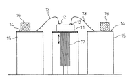
図2を用いて説明する。11はICチップ、12はAl電極、13は金合金線、14はリードフレーム、15は鉄製台、16はリードフレーム固定用磁石、17は振動子である。リードフレーム14をリードフレーム固定用磁石16で固定し、ICチップ11を搭載した部分を振動子17で上下方向(矢印方向)に振動させた。周波数100Hz、上下振幅合計0.4mm、振動数20000回振動させた後、400倍の金属顕微鏡を用いてリードフレーム側即ちセカンド側のワイヤの破断数を調査した。300箇所調査しその破断数の割合を振動破断率として表1に示した。
(実施例2〜52)(比較例1〜10)
金合金線の組成を表1〜3に示すようにしたこと以外は実施例1と同様にして直径30μmの線に仕上げ、熱サイクル後の破断率、セカンド側のピール強度及び振動破断率を実施例1と同様にして測定し、その測定結果を表1〜3に示した。
【0024】
【表1】

【表2】
【表3】
(試験結果)
(1)高純度金にInを1〜50重量ppm 、Snを1〜50重量ppm 、La,Ce,Eu,Ybのうち少なくとも1種を1〜50重量ppm 及びAg,Pt,Pd,Rh,Ir,Os,Ruのうち少なくとも1種を1〜100重量ppm 含有した組成である実施例1〜40は熱サイクル後の破断率が1.9%以下であり、ピール強度は7.2〜13.6g、振動破断率は1.8%以下と優れた効果を示した。
【0028】
(2)この中でもLa,Ce,Eu,Ybのうち少なくとも1種がLaである組成では熱サイクル後の破断率が0.6%以下であり、ピール強度は11.2〜13.6g、振動破断率は0.9%以下とさらに優れた効果を示した。
この為好ましくはLa,Ce,Eu,Ybのうち少なくとも1種がLaである組成とすることである。
【0029】
(3)更にLa,Ce,Eu,Ybのうち少なくとも1種がLaである組成とすることに加えて、Ag,Pt,Pd,Rh,Ir,Os,Ruのうち少なくとも1種を9〜100重量ppm 含有した組成とすることにより、熱サイクル後の破断率が0%であり、ピール強度は12.7〜13.6g、振動破断率は0%と最も優れた効果を示した。
【0030】
この為最も好ましくはLa,Ce,Eu,Ybのうち少なくとも1種がLaである組成とすることに加えて、Ag,Pt,Pd,Rh,Ir,Os,Ruのうち少なくとも1種を9〜100重量ppm 含有した組成とすることである。
(4)高純度金に所定量のInと所定量のSnと所定量のLa,Ce,Eu,Ybのうち少なくとも1種と所定量のAg,Pt,Pd,Rh,Ir,Os,Ruのうち少なくとも1種との共存において、Ca,Ge,Beのうち少なくとも1種を50重量ppm 以下含有した組成である実施例41〜52においても同様の効果が得られる事が判る。
【0031】
(5)本発明の必須成分の何れも含有しない高純度金を用いた比較例1は熱サイクル後の破断率が5.9%、ピール強度は1.6g、振動破断率は4.9%と何れも悪いものであった。
(6)高純度金に本発明の必須成分を所定量含有するものの、Inの含有量が1重量ppm 未満である比較例2、その含有量が50重量ppm を超える比較例3は、熱サイクル後の破断率が2.4〜3.2%、ピール強度は3.1〜4.2g、振動破断率は2.4〜3.3%と何れも高純度金と対比すると効果は得られているものの、本発明の効果の方が優れていることが判る。
【0032】
(7)高純度金に本発明の必須成分を所定量含有するものの、Snの含有量が1重量ppm 未満である比較例4〜5、その含有量が50重量ppm を超える比較例6は熱サイクル後の破断率が2.6〜3.8%、ピール強度は3.0〜4.1g、振動破断率は3.0〜3.9%と何れも高純度金と対比すると効果は得られているものの、本発明の効果の方が優れていることが判る。
【0033】
(8)高純度金にLa,Ce,Eu,Ybのうち少なくとも1種以外の本発明の必須成分を所定量含有するものの本発明の必須成分である所定量のLa,Ce,Eu,Ybのうち少なくとも1種を含有しない比較例7〜10は、熱サイクル後の破断率が3.5〜3.9%、ピール強度は2.3〜2.8g、振動破断率は3.6〜3.9%と何れも高純度金と対比すると効果は得られているものの、本発明の効果の方が優れていることが判る。
【0034】
とりわけ比較例8〜10は本発明の必須元素としてLa,Ce,Eu,Ybのうち少なくとも1種にかえて同じ希土類元素であるPr,Pm,Luを用いた場合本発明のような優れた効果が得られない事が判る。
即ち本発明に必要な必須元素の一つは希土類元素ではなくLa,Ce,Eu,Ybのうち少なくとも1種であることが判る。
【0035】
(9)高純度金にLa,Ce,Eu,Ybのうち少なくとも1種以外の本発明の必須成分を所定量含有するものの本発明の必須成分である所定量のLa,Ce,Eu,Ybのうち少なくとも1種を含有しない比較例7は、熱サイクル後の破断率が3.1%、ピール強度は2.7g、振動破断率は3.0%と何れも高純度金と対比すると効果は得られているものの、本発明の効果の方が優れていることが判る。
【0036】
【発明の効果】
本発明により所定量のIn、所定量のSn、所定量のLa,Ce,Eu,Ybのうち少なくとも1種、所定量のAg,Pt,Pd,Rh,Ir,Os,Ruのうち少なくとも1種を含有し残部が金及び不純物からなる組成を有する半導体素子ボンディング用金合金線によれば、銅合金製のリードフレームを用いた半導体装置が過酷な熱サイクルの環境に晒された場合でも、断線を抑制する効果が向上すること及びボンディング時のループ形状を安定させる為に、ボンディング時の加熱温度を150℃と低温度で行いながらセカンド側接合点での接合性、とりわけピール強度及び振動破断性能が向上に効果的である。
【0037】
前記含有成分に加えて所定量のCa,Ge,Beのうち少なくとも1種を含有した場合においても、同様の効果を示すものである。
【図面の簡単な説明】
【図1】金合金線でボンディングした半導体素子を示す。
【図2】振動破断性能の測定方法を示す。
【符号の説明】
1…ICチップ
2…ICチップの電極
3…金合金線
4…リードフレーム
5…ファースト側接合点
6…セカンド側接合点[0001]
BACKGROUND OF THE INVENTION
The present invention relates to a gold alloy wire for bonding used for connecting an electrode of a semiconductor element and an external lead portion.
[0002]
[Prior art]
Conventionally, as a technology for connecting electrodes of semiconductor elements such as transistors, ICs and LSIs and external leads, a gold alloy wire in which a trace amount of other metal elements is contained in high-purity gold having a purity of 99.99% by weight or more is used. An ultrasonic combined thermocompression bonding method for wiring is mainly used.
[0003]
Here, FIG. 1 shows a state where wiring is formed by a thermocompression bonding method using ultrasonic waves and a loop is formed. Reference numeral 1 is an IC chip, 2 is an Al electrode on the IC chip, 3 is a gold alloy wire, 4 is a lead frame, 5 is a first side junction, and 6 is a second side junction. Recently, semiconductor devices have increasingly used copper alloy lead frames as external lead materials in consideration of heat dissipation and cost. When a copper alloy lead frame is used, the difference in thermal expansion coefficient between the sealing resin and the lead frame is large, and external stress is applied to the gold alloy wire that forms a loop due to the temperature rise caused by the operation of the semiconductor device. When the apparatus is exposed to a severe heat cycle environment, there is a problem that disconnection is likely to occur.
[0004]
In addition, with increasing demands for miniaturization and higher density of semiconductor devices, there are demands for a multi-pin IC chip and a narrow pitch associated therewith. In order to achieve multiple pins and narrow pitch, it is necessary that the loop shape is stable. On the other hand, when wiring is carried out by the ultrasonic combined thermocompression bonding method, the wiring is heated at 150 to 250 ° C. by a heat source installed at the lower part of the lead frame. At this time, if the heating temperature is high, the adhesiveness is good, but the lead frame is likely to warp and the loop shape tends to vary. In addition, when the heating temperature is low, the loop shape is stable, but it is a low-temperature bonding, which causes a problem in the bonding property at the bonding point between the gold alloy wire and the lead frame (hereinafter referred to as the second-side bonding point). For this reason, in order to suppress the variation in the loop shape, a gold alloy wire excellent in bondability at the second side bonding point is required while performing the heating temperature during bonding at a low temperature of 150 ° C.
[0005]
As a conventionally proposed gold alloy wire, Japanese Patent Application Laid-Open No. 3-257129 proposes that a predetermined amount of La, Ca, Sn or the like is contained in gold and is effective in loop deformation. Japanese Patent Application Laid-Open No. 8-291348 proposes that a predetermined amount of La, Ca, In, or the like is contained in gold so that the bonding strength is effective.
[0006]
[Problems to be solved by the invention]
However, the proposal is still insufficient for the aforementioned requirements.
The present invention has been made in view of the circumstances as described above, and the object is to break even when a semiconductor device using a copper alloy lead frame is exposed to a severe thermal cycle environment. In order to improve the effect of suppressing cracking and to stabilize the loop shape during bonding, the bonding property at the second side junction, especially the peel strength and vibration breakage, while the heating temperature during bonding is performed at a low temperature of 150 ° C. It is to provide a gold alloy wire with improved performance.
[0007]
[Means for Solving the Problems]
As a result of extensive studies by the present inventors, at least one of a predetermined amount of In, Sn, La, Ce, Eu, and Yb and at least one of Ag, Pt, Pd, Rh, Ir, Os, and Ru. And, it was found that the above-mentioned object can be achieved by using a gold alloy wire having a composition consisting of gold and inevitable impurities, and the present invention has been completed.
[0008]
That is, the present invention is as follows.
(1) 1 to 50 ppm by weight of indium (In), 1 to 50 ppm by weight of tin (Sn), 1 to 50 ppm by weight of at least one of La, Ce, Eu, and Yb, Ag, Pt, Pd, A gold alloy wire for bonding semiconductor elements, wherein at least one of Rh, Ir, Os, and Ru is 1 to 100 ppm by weight, and the balance is made of gold and inevitable impurities.
(2) The gold alloy wire for bonding a semiconductor element according to claim 1, wherein at least one of Ca, Ge, and Be is added in an amount of 50 ppm by weight or less.
(3) The gold alloy wire for bonding a semiconductor element according to claim 1 or 2, wherein at least one of La, Ce, Eu, and Yb is La.
(4) The gold alloy wire for bonding semiconductor elements according to claim 3, wherein the content of at least one of Ag, Pt, Pd, Rh, Ir, Os, and Ru is 9 to 100 ppm by weight.
[0009]
DETAILED DESCRIPTION OF THE INVENTION
It is preferable to use high-purity gold purified to at least 99.99% by weight or more as a raw material. More preferably, it is 99.995 weight% or more, Most preferably, it is 99.999 weight% or more. Therefore, the inevitable impurities in the alloy are preferably 0.01% by weight or less. More preferably, it is 0.005 weight% or less, Most preferably, it is 0.001 weight% or less.
[0010]
In high-purity gold coexisting with a predetermined amount of Sn and at least one of a predetermined amount of La, Ce, Eu, Yb and at least one of a predetermined amount of Ag, Pt, Pd, Rh, Ir, Os, Ru The above problem can be achieved by using a composition containing a predetermined amount of In.
In this coexisting composition, when the In content is 1 ppm by weight or more, the second-side bondability is improved as compared with the content of less than 1 ppm by weight. That is, the peel strength is increased and the vibration breaking performance is improved. Also, the disconnection performance after the thermal cycle is improved. If the In content exceeds 50 ppm by weight, both the second-side bondability and the disconnection performance after thermal cycling will be degraded. For this reason, the content of In in the coexisting composition is set to 1 to 50 ppm by weight.
[0011]
In high-purity gold coexisting with a predetermined amount of In and at least one of a predetermined amount of La, Ce, Eu, Yb and at least one of a predetermined amount of Ag, Pt, Pd, Rh, Ir, Os, Ru The above problem can be achieved by using a composition containing a predetermined amount of Sn.
In this coexisting composition, when the Sn content is 1 ppm by weight or more, the second-side bondability is improved and the disconnection performance after the thermal cycle is improved as compared with the content of less than 1 ppm by weight. If the Sn content exceeds 50 ppm by weight, both the second-side bondability and the disconnection performance after thermal cycling are degraded. Therefore, the Sn content in the coexisting composition is set to 1 to 50 ppm by weight.
[0012]
In the presence of a predetermined amount of In, a predetermined amount of Sn, and a predetermined amount of Ag, Pt, Pd, Rh, Ir, Os, Ru in high-purity gold, a predetermined amount of La, Ce, Eu, Yb The said subject can be achieved by setting it as the composition containing at least 1 sort (s) among these.
In this coexisting composition, when the content of at least one of La, Ce, Eu, and Yb is 1 ppm by weight or more, the second-side bondability is improved and the thermal cycle is improved as compared with the content of less than 1 ppm by weight. Later disconnection performance will also improve. If the content of at least one of La, Ce, Eu, and Yb exceeds 50 ppm by weight, both the second-side bondability and the disconnection performance after thermal cycling are degraded. Therefore, the content of at least one of La, Ce, Eu, and Yb in the coexisting composition is set to 1 to 50 ppm by weight.
[0013]
At least one of La, Ce, Eu, and Yb in the coexisting composition cannot be replaced with another rare earth element. By using at least one of La, Ce, Eu, and Yb among rare earth elements, the above-described problem can be achieved.
Furthermore, when at least one of La, Ce, Eu, and Yb in the coexisting composition is La, the second-side bondability and the disconnection performance after thermal cycling are further improved.
[0014]
Therefore, at least one of La, Ce, Eu, and Yb in the coexisting composition is preferably La.
In the presence of a predetermined amount of In, a predetermined amount of Sn, and a predetermined amount of La, Ce, Eu, Yb in high-purity gold, a predetermined amount of Ag, Pt, Pd, Rh, Ir, Os, Ru The said subject can be achieved by setting it as the composition containing at least 1 sort (s) among these.
[0015]
In this coexisting composition, when the content of at least one of Ag, Pt, Pd, Rh, Ir, Os, and Ru is 1 ppm by weight or more, the second-side bondability is improved as compared to the content of less than 1 ppm by weight. As a result, the disconnection performance after thermal cycling will also improve. If the content of at least one of Ag, Pt, Pd, Rh, Ir, Os, and Ru exceeds 100 ppm by weight, both the second-side bondability and the disconnection performance after thermal cycling are degraded. Therefore, the content of at least one of Ag, Pt, Pd, Rh, Ir, Os, and Ru in the coexisting composition is set to 1 to 100 ppm by weight.
[0016]
Further, at least one of La, Ce, Eu and Yb in the coexisting composition is La, and the content of at least one of Ag, Pt, Pd, Rh, Ir, Os and Ru is 9 to 100 ppm by weight. Sometimes the second side bondability and the disconnection performance after thermal cycling are most improved. Therefore, in the coexisting composition, at least one of La, Ce, Eu, and Yb is La, and the content of at least one of Ag, Pt, Pd, Rh, Ir, Os, and Ru is 9 to 100 weights. Most preferred is ppm.
[0017]
At least one of a predetermined amount of In, a predetermined amount of Sn, and a predetermined amount of La, Ce, Eu, Yb and a predetermined amount of Ag, Pt, Pd, Rh, Ir, Os, Ru in high purity gold In the coexistence with the seed, the same effect can be obtained even when the composition contains at least one of Ca, Ge, and Be in an amount of 50 ppm by weight or less.
[0018]
A preferred method for producing a gold alloy wire according to the present invention will be described.
A predetermined amount of element is added to high-purity gold, melted in a vacuum melting furnace, and cast into an ingot. The ingot is subjected to cold working and intermediate annealing using a groove roll and a wire drawing machine, and is subjected to final annealing after forming a thin wire having a diameter of 10 to 100 μm by final cold working.
[0019]
The gold alloy wire for bonding a semiconductor element according to the present invention is preferably used in an ultrasonic combined thermocompression bonding method for connecting a semiconductor element such as an IC chip to a lead frame when mounting a semiconductor device. In particular, it is preferably used for a semiconductor device using a copper lead frame as the lead frame.
[0020]
【Example】
(Example 1)
A predetermined amount of In, Sn, La, Ag was added to high-purity gold having a purity of 99.999% by weight, melted in a vacuum melting furnace, and then cast to obtain a gold alloy ingot having the composition shown in Table 1. This was subjected to cold working and intermediate annealing using a groove roll and a wire drawing machine, and final annealing was performed so that the final cold working had a diameter of 30 μm and an elongation rate of 4%.
[0021]
The gold alloy wire was bonded to the Al electrode of the IC chip and the copper alloy lead frame by an ultrasonic combined thermocompression bonding method at a heating temperature of 150 ° C. using a fully automatic wire bonder (UTC-50 type manufactured by Shinkawa Co., Ltd.). Then, a bonded sample having 100 pins was prepared. Next, after sealing the sample with an epoxy resin, a thermal cycle test was performed 100 times at −10 ° C. × 30 minutes and 150 ° C. × 30 minutes.
[0022]
100 samples were subjected to measurement, the presence or absence of disconnection was confirmed by a continuity test, the fracture rate after thermal cycling was determined, and the results are shown in Table 1.
Further, the peel strength and vibration breaking performance on the lead frame side, that is, the second side of the bonded sample were measured. The peel strength was indicated by the peel load having a diameter of 30 μm.
[0023]
Method for Measuring Vibration Breaking Performance A description will be given with reference to FIG. 11 is an IC chip, 12 is an Al electrode, 13 is a gold alloy wire, 14 is a lead frame, 15 is an iron base, 16 is a lead frame fixing magnet, and 17 is a vibrator. The
(Examples 2 to 52) (Comparative Examples 1 to 10)
Except that the composition of the gold alloy wire is as shown in Tables 1 to 3, it was finished to a wire having a diameter of 30 μm in the same manner as in Example 1, and the fracture rate after the thermal cycle, the peel strength on the second side, and the vibration fracture rate were carried out. The measurement was performed in the same manner as in Example 1, and the measurement results are shown in Tables 1 to 3.
[0024]
[Table 1]
[Table 2]
[Table 3]
(Test results)
(1) In high-purity gold, 1 to 50 ppm by weight of In, 1 to 50 ppm by weight of Sn, 1 to 50 ppm by weight of at least one of La, Ce, Eu, and Yb, and Ag, Pt, Pd, Rh, In Examples 1 to 40 having a composition containing 1 to 100 ppm by weight of at least one of Ir, Os, and Ru, the breaking rate after thermal cycling is 1.9% or less, and the peel strength is 7.2 to 13 .6 g, and the vibration breaking rate was 1.8% or less, showing an excellent effect.
[0028]
(2) Among these, a composition in which at least one of La, Ce, Eu, and Yb is La has a fracture rate after thermal cycling of 0.6% or less, a peel strength of 11.2 to 13.6 g, and vibration. The breakage rate was 0.9% or less, showing a further excellent effect.
For this reason, the composition is preferably such that at least one of La, Ce, Eu, and Yb is La.
[0029]
(3) Furthermore, in addition to a composition in which at least one of La, Ce, Eu, and Yb is La, at least one of Ag, Pt, Pd, Rh, Ir, Os, and Ru is 9 to 100. By using a composition containing ppm by weight, the breaking rate after thermal cycling was 0%, the peel strength was 12.7 to 13.6 g, and the vibration breaking rate was 0%, showing the most excellent effects.
[0030]
Therefore, most preferably, in addition to a composition in which at least one of La, Ce, Eu, and Yb is La, at least one of Ag, Pt, Pd, Rh, Ir, Os, and Ru is 9 to 9 The composition should contain 100 ppm by weight.
(4) At least one of a predetermined amount of In, a predetermined amount of Sn, and a predetermined amount of La, Ce, Eu, Yb and a predetermined amount of Ag, Pt, Pd, Rh, Ir, Os, Ru It turns out that the same effect is acquired also in Examples 41-52 which are the compositions containing 50 weight ppm or less of at least 1 sort (s) among Ca, Ge, and Be in coexistence with at least 1 sort (s).
[0031]
(5) Comparative Example 1 using high-purity gold containing none of the essential components of the present invention has a breaking rate after thermal cycling of 5.9%, a peel strength of 1.6 g, and a vibration breaking rate of 4.9%. Both were bad.
(6) Although a predetermined amount of the essential component of the present invention is contained in high purity gold, the comparative example 2 in which the content of In is less than 1 ppm by weight, and the comparative example 3 in which the content exceeds 50 ppm by weight The later breakage rate is 2.4-3.2%, peel strength is 3.1-4.2g, and vibration breakage rate is 2.4-3.3%. However, it can be seen that the effect of the present invention is superior.
[0032]
(7) Although high purity gold contains the essential component of the present invention in a predetermined amount, Comparative Examples 4 to 5 in which the Sn content is less than 1 ppm by weight, and Comparative Example 6 in which the content exceeds 50 ppm by weight are heat After the cycle, the breaking rate is 2.6 to 3.8%, the peel strength is 3.0 to 4.1 g, and the vibration breaking rate is 3.0 to 3.9%. However, it can be seen that the effect of the present invention is superior.
[0033]
(8) Although high-purity gold contains a predetermined amount of La, Ce, Eu, Yb other than La, Ce, Eu, Yb, the present invention contains a predetermined amount of La, Ce, Eu, Yb that is an essential component of the present invention. Of Comparative Examples 7 to 10 not containing at least one of them, the breaking rate after thermal cycling is 3.5 to 3.9%, the peel strength is 2.3 to 2.8 g, and the vibration breaking rate is 3.6 to 3 It can be seen that the effect of the present invention is superior, although an effect is obtained when .9% is compared with high purity gold.
[0034]
In particular, Comparative Examples 8 to 10 have excellent effects as in the present invention when Pr, Pm, and Lu, which are the same rare earth elements, are used instead of at least one of La, Ce, Eu, and Yb as essential elements of the present invention. It turns out that cannot be obtained.
That is, it can be seen that one of the essential elements necessary for the present invention is not a rare earth element but at least one of La, Ce, Eu, and Yb.
[0035]
(9) Although high-purity gold contains a predetermined amount of La, Ce, Eu, Yb at least one essential component of the present invention, a predetermined amount of La, Ce, Eu, Yb that is an essential component of the present invention Of these, Comparative Example 7, which does not contain at least one kind, had an effect when compared to high-purity gold, with a breaking rate after thermal cycling of 3.1%, a peel strength of 2.7 g, and a vibration breaking rate of 3.0%. Although obtained, it can be seen that the effect of the present invention is superior.
[0036]
【The invention's effect】
According to the present invention, at least one of a predetermined amount of In, a predetermined amount of Sn, and a predetermined amount of La, Ce, Eu, Yb, and at least one of a predetermined amount of Ag, Pt, Pd, Rh, Ir, Os, Ru. According to the gold alloy wire for bonding a semiconductor element, the balance of which is composed of gold and impurities, the semiconductor device using the copper alloy lead frame is disconnected even when exposed to a severe thermal cycle environment. In order to improve the effect of suppressing cracking and stabilize the loop shape at the time of bonding, the bonding property at the second side bonding point, particularly the peel strength and vibration breaking performance, while performing the heating temperature at the time of bonding at a low temperature of 150 ° C. Is effective for improvement.
[0037]
Even when at least one of a predetermined amount of Ca, Ge, and Be is contained in addition to the above-described components, the same effect is exhibited.
[Brief description of the drawings]
FIG. 1 shows a semiconductor element bonded with a gold alloy wire.
FIG. 2 shows a method for measuring vibration breaking performance.
[Explanation of symbols]
DESCRIPTION OF SYMBOLS 1 ... IC chip 2 ... IC chip electrode 3 ...
Claims (2)
Priority Applications (1)
| Application Number | Priority Date | Filing Date | Title |
|---|---|---|---|
| JP10896197A JP3669809B2 (en) | 1997-04-25 | 1997-04-25 | Gold alloy wire for semiconductor element bonding |
Applications Claiming Priority (1)
| Application Number | Priority Date | Filing Date | Title |
|---|---|---|---|
| JP10896197A JP3669809B2 (en) | 1997-04-25 | 1997-04-25 | Gold alloy wire for semiconductor element bonding |
Publications (2)
| Publication Number | Publication Date |
|---|---|
| JPH10303235A JPH10303235A (en) | 1998-11-13 |
| JP3669809B2 true JP3669809B2 (en) | 2005-07-13 |
Family
ID=14498053
Family Applications (1)
| Application Number | Title | Priority Date | Filing Date |
|---|---|---|---|
| JP10896197A Expired - Fee Related JP3669809B2 (en) | 1997-04-25 | 1997-04-25 | Gold alloy wire for semiconductor element bonding |
Country Status (1)
| Country | Link |
|---|---|
| JP (1) | JP3669809B2 (en) |
Families Citing this family (7)
| Publication number | Priority date | Publication date | Assignee | Title |
|---|---|---|---|---|
| KR20010073501A (en) * | 2000-01-17 | 2001-08-01 | 강도원 | A alloy of bonding wire for high stretch using for semiconductor packaging |
| JP3323185B2 (en) * | 2000-06-19 | 2002-09-09 | 田中電子工業株式会社 | Gold wire for connecting semiconductor elements |
| JP4513440B2 (en) * | 2004-07-15 | 2010-07-28 | 住友ベークライト株式会社 | Semiconductor device |
| KR100929432B1 (en) * | 2004-11-26 | 2009-12-03 | 타나카 덴시 코오교오 카부시키가이샤 | Au bonding wire for semiconductor devices |
| JP4726205B2 (en) * | 2005-06-14 | 2011-07-20 | 田中電子工業株式会社 | Gold alloy wire for bonding wire with high initial bondability, high bond reliability, high roundness of crimped ball, high straightness and high resin flow resistance |
| KR100801444B1 (en) * | 2006-05-30 | 2008-02-11 | 엠케이전자 주식회사 | Au-Ag based alloy wire for a semiconductor package |
| JP4150752B1 (en) * | 2007-11-06 | 2008-09-17 | 田中電子工業株式会社 | Bonding wire |
-
1997
- 1997-04-25 JP JP10896197A patent/JP3669809B2/en not_active Expired - Fee Related
Also Published As
| Publication number | Publication date |
|---|---|
| JPH10303235A (en) | 1998-11-13 |
Similar Documents
| Publication | Publication Date | Title |
|---|---|---|
| CN102154574A (en) | Alloy wire for connecting semiconductor components | |
| JP3669809B2 (en) | Gold alloy wire for semiconductor element bonding | |
| JP3527356B2 (en) | Semiconductor device | |
| JP3628139B2 (en) | Gold alloy wire for semiconductor element bonding | |
| JP3669811B2 (en) | Gold alloy wire for semiconductor element bonding | |
| JP3654736B2 (en) | Gold alloy wire for semiconductor element bonding | |
| JP3669810B2 (en) | Gold alloy wire for semiconductor element bonding | |
| JPH10233408A (en) | Metal junction structure and semiconductor device | |
| JP3615897B2 (en) | Gold alloy wire for semiconductor element bonding | |
| JP3751104B2 (en) | Gold alloy wire for semiconductor element bonding | |
| JP3810200B2 (en) | Gold alloy wire for wire bonding | |
| JP2962351B2 (en) | Bonding structure to semiconductor chip and semiconductor device using the same | |
| JPH10303238A (en) | Gold alloy wire for bonding on semiconductor device | |
| JP3585993B2 (en) | Gold wire for bonding | |
| JP3916320B2 (en) | Gold alloy wire for bonding | |
| JP3615901B2 (en) | Gold alloy wire for semiconductor element bonding | |
| JP3689234B2 (en) | Micro gold ball for bump and semiconductor device | |
| JP4117973B2 (en) | Gold alloy wire for bonding | |
| JPH09275119A (en) | Semiconductor device | |
| JPH0413858B2 (en) | ||
| JP3104442B2 (en) | Bonding wire | |
| JPH10275823A (en) | Gold alloy ball for bump | |
| JPH09272930A (en) | Fine gold alloy wire for bump, and gold alloy bump | |
| JP2556084B2 (en) | Cu alloy extra fine wire for semiconductor devices | |
| JP3235199B2 (en) | Bonding wire |
Legal Events
| Date | Code | Title | Description |
|---|---|---|---|
| A521 | Written amendment |
Free format text: JAPANESE INTERMEDIATE CODE: A523 Effective date: 20040409 |
|
| A621 | Written request for application examination |
Free format text: JAPANESE INTERMEDIATE CODE: A621 Effective date: 20040409 |
|
| A977 | Report on retrieval |
Free format text: JAPANESE INTERMEDIATE CODE: A971007 Effective date: 20041222 |
|
| A131 | Notification of reasons for refusal |
Free format text: JAPANESE INTERMEDIATE CODE: A131 Effective date: 20050104 |
|
| TRDD | Decision of grant or rejection written | ||
| A01 | Written decision to grant a patent or to grant a registration (utility model) |
Free format text: JAPANESE INTERMEDIATE CODE: A01 Effective date: 20050315 |
|
| A61 | First payment of annual fees (during grant procedure) |
Free format text: JAPANESE INTERMEDIATE CODE: A61 Effective date: 20050412 |
|
| R150 | Certificate of patent or registration of utility model |
Free format text: JAPANESE INTERMEDIATE CODE: R150 |
|
| S531 | Written request for registration of change of domicile |
Free format text: JAPANESE INTERMEDIATE CODE: R313531 |
|
| R350 | Written notification of registration of transfer |
Free format text: JAPANESE INTERMEDIATE CODE: R350 |
|
| FPAY | Renewal fee payment (event date is renewal date of database) |
Free format text: PAYMENT UNTIL: 20090422 Year of fee payment: 4 |
|
| FPAY | Renewal fee payment (event date is renewal date of database) |
Free format text: PAYMENT UNTIL: 20100422 Year of fee payment: 5 |
|
| FPAY | Renewal fee payment (event date is renewal date of database) |
Free format text: PAYMENT UNTIL: 20110422 Year of fee payment: 6 |
|
| LAPS | Cancellation because of no payment of annual fees |