JP3666528B2 - Reflective liquid crystal display - Google Patents
Reflective liquid crystal display Download PDFInfo
- Publication number
- JP3666528B2 JP3666528B2 JP29897696A JP29897696A JP3666528B2 JP 3666528 B2 JP3666528 B2 JP 3666528B2 JP 29897696 A JP29897696 A JP 29897696A JP 29897696 A JP29897696 A JP 29897696A JP 3666528 B2 JP3666528 B2 JP 3666528B2
- Authority
- JP
- Japan
- Prior art keywords
- liquid crystal
- reflective
- crystal display
- layer
- display device
- Prior art date
- Legal status (The legal status is an assumption and is not a legal conclusion. Google has not performed a legal analysis and makes no representation as to the accuracy of the status listed.)
- Expired - Lifetime
Links
Images


Description
【0001】
【発明の属する技術分野】
本発明は反射型液晶表示装置に係り、特に、反射光に起因する表示態様を改善することによって、その視認性を向上させるための技術に関する。
【0002】
【従来の技術】
従来、液晶表示装置としては、TN(Twisted Nematic)型液晶表示素子、STN(Super Twisted Nematic)型液晶表示素子、強誘電液晶表示素子等の種々の形式の装置がある。これらの中には、偏光板を用いることにより液晶の電界効果に基づく光の偏光状態の変化を利用して表示の切り替えを行うものと、偏光板を用いることなく、液晶の相変化、配向状態の変化その他の変化により光透過状態と光散乱状態とを切り替え可能にするものとがある。
【0003】
後者の液晶表示装置においては、偏光板を使用しないので、光の利用効率が高く、明るい表示を得ることができるという利点がある。この場合の表示特性は、光透過状態における透明度と、光散乱状態における散乱強度若しくは反射率とによってほぼ決定される。
【0004】
従来使用されている偏光板を使用しない液晶表示装置の例としては、図10に示す高分子分散型の液晶表示装置がある。この装置においては、基板1の内面上にITO(Indium Tin Oxide)等からなる電極3が形成され、また、基板2の内面上にはAl、Cr等からなる反射層を兼ねた金属電極4が形成されている。基板1及び透明電極3の表面上にはポリイミド、ポリビニルアルコール等からなる配向膜5が形成され、基板2及び金属電極4の表面上には同様の配向膜6が形成されている。これらの配向膜5,6には図中矢印で示すa方向にラビング処理が施されている。
【0005】
上記基板1及び基板2は、シール材やスペーサ等により所定間隔(例えば5〜10μm)を隔てて対向する状態に保持され、両基板の間に液晶高分子複合層7が封入されている。この液晶高分子複合層7は、液晶7Aの中に高分子7Bの粒子が分散したものであり、液晶7A及び高分子7Bは共に配向膜5と6に施されたラビングの方向に配向している。
【0006】
透明電極3と金属電極4との間に電圧を印加しない電界無印加状態においては、図10(a)に示すように配向方向の揃った液晶7A及び高分子7Bとがほぼ同様の屈折率を呈するため、液晶高分子複合層7は光透過状態となり、反射層である金属電極4により入射光はそのまま反射される。一方、透明電極3と金属電極4との間に所定の電圧を印加すると、図10(b)に示すように誘電異方性を備えた液晶7Aは電界方向bに配向するため、屈折率異方性を呈する液晶7Aと高分子7Bとの間に屈折率の差が生じ、液晶高分子複合層7は光散乱状態となり、入射光は散乱される。
【0007】
上述のような高分子分散型の液晶表示装置の種々の構造及び製法は、アメリカ特許公報第3600060号や特開平5−119302号公報等に詳細に記載されている。
【0008】
一方、液晶表示装置としてはカラー表示を可能とするためにカラーフィルタを形成したものがある。このようなカラー表示を可能とした液晶表示装置としては例えば図11に示す断面構造を備えたものがある。この液晶表示装置は反射型であり、一方の基板である透明基板11の内面上に透明電極13を被着し、その上に配向膜14を塗布して所定方向にラビング処理を施している。他方の基板である透明基板12の内面上にはCr、Al等の金属からなる金属電極15が形成され、この金属電極15の表面上に所定の配列方法で配列された着色層(赤色部)16a、(青色部)16b、(緑色部)16cを備えたカラーフィルタ16が形成されている。このカラーフィルタ16の表面上には上述と同様の配向膜17が被着される。
【0009】
これらの透明基板11と透明基板12とは、上記と同様に図示しないシール材を介して貼り合わせられ、シール材に囲まれた領域内に液晶を封入することにより液晶層18が形成される。
【0010】
このように形成された反射型液晶表示体においては、透明基板11の側から入射した光が液晶層18、カラーフィルタ16を順次透過して金属電極15にて反射され、再びカラーフィルタ16、液晶層18を介して透明基板11から放出されるように構成されているので、透明電極13と金属電極15との間に所定の電圧を印加することによって液晶層18が配向制御され、この液晶層18の光学的特性の変化により所望のカラー表示を行うことができる。
【0011】
なお、反射型液晶表示装置においては、上記のように透明基板の内側に金属によって形成された反射層を形成する以外に、透明基板の外側に反射層を形成する場合や、基板そのものを反射性の材料で構成する場合等がある。
【0012】
【発明が解決しようとする課題】
上記のように、液晶を用いた種々の形式により表示を行う各種の液晶表示装置が開発され、実用に供されている。この場合、反射型の液晶表示装置においてはバックライト等の光源を必要とせず、消費電力を低減できることから、携帯用機器等に使用する場合に適している。その反面、反射型の場合には一般に表示が暗く、しかも表示のコントラストを十分に高めることが困難であるという問題点がある。
【0013】
このため、反射型の液晶表示装置においては、表示の明るさ及びコントラストの向上を図ることが技術的課題の最も重要なものとなっており、この技術的課題を解決するために種々の開発が行われている。上述の光散乱によって表示を行う形式の表示素子もその開発の成果のうちのひとつであり、明るい表示と良好なコントラストを示す表示素子が製造可能となっている。
【0014】
ところが、反射型の液晶表示装置において表示の明るさとコントラストの向上を図った場合、上記の金属電極によって反射される光が表示の視認性を損なわせるという問題がある。これは、表示の明るさとコントラストの向上を図るために金属電極等によって形成された反射層はほとんど鏡と同様に高い反射率を呈するように形成されているため、液晶層の光透過状態における透明度が高いと、表示画面に周囲の景色が映ってしまったり、照明から発せられた直射光が使用者の目に入って眩惑させたりすることがあるからである。
【0015】
このような反射型液晶表示装置の視認性は、ノングレア板その他のフィルタを取り付けることによって多少は改善されるが、これらのフィルタによって表示の明るさが減退したりコントラストが低下したりすることはあっても、背景の映り込み等の表示品位の基本的な特性を変えることはできず、視認性の大幅な改善は困難であった。
【0016】
また、上述の光散乱を利用した表示素子の場合には、光透過状態における透過率の向上によって表示の明るさを確保し、コントラストを向上させるという改善がなされているが、このような改善を行う程、背景の映り込みや直射光による幻惑はさらに顕著なものとなるという問題点がある。
【0017】
そこで本発明は上記問題点を解決するものであり、その課題は、反射型液晶表示素子における反射層の光反射に起因する視認性の低下を防止する新規の技術を提供することにある。
【0018】
【課題を解決するための手段】
上記課題を解決するために本発明が講じた手段は、対向する内面に電極を有する一対の基板間に液晶層を挟持してなり、前記一方の基板の前記液晶層に対向する側に反射層を備え、対向する前記電極によって複数の画素領域が構成され、前記液晶層には、前記画素領域毎に、反射率が高い反射区画と、反射率が低い反射区画とが形成され、前記反射率が高い反射区画は光学的鏡面であり、前記反射率が低い反射区画は凹凸が形成されてなることを特徴とする。
【0019】
この手段によれば、画素領域毎に反射率の異なる複数の反射区画が形成されているため、一方の基板から入射された光は、反射区画の反射率の相違によって各画素領域内においてそれぞれ変調されるので、液晶層が透明状態になっても、背景が映し込まれたり、直射光がそのままの状態で目に入ったりすることがなくなるから、画素領域によって形成される表示に影響を与えることなく、液晶表示装置の視認性を向上させることができる。
【0020】
ここで、前記液晶層に印加される電圧の印加状態により光透過状態と光散乱状態との間の光学特性を制御してなることを特徴とする。また、前記複数の反射区画は、前記液晶層に対して電位を印加するための裏面側電極として形成されたものであることが好ましい。この場合には、反射区画が裏面側電極で構成されているために、反射層を別途設ける必要がなく、電極形成工程で同時に作り込むことができる。
【0021】
前記反射率が高い反射区画と低い反射区画とは、相互に異なる種類の材料を含んで形成され、若しくは異なる膜厚で形成されても良い。
【0022】
金属その他の反射性材料の種類や組成または形成条件を変えることにより反射率の異なる反射区画を容易に形成することができる。
【0023】
次に、別の手段としては、対向する内面に電極を有する一対の基板間に液晶を挟持してなり、前記一方の基板に反射層を備え、該反射層に対して前記他方の基板側に形成された複数の色要素からなるカラーフィルターが配置されてなり、対向する前記電極によって複数の画素領域が構成され、前記液晶層に印加される電圧の印加状態により液晶層を制御してなり、前記カラーフィルターは前記画素領域内に対応して形成されてなり、前記カラーフィルタは、前記画素領域内において所定の平面パターンで選択的に形成されていることを特徴とする。
【0024】
この手段によれば、カラーフィルタが画素領域内において所定の平面パターンで選択的に形成されているため、一方の基板から入射された光は、カラーフィルタを透過する際に、各画素領域内においてそれぞれカラーフィルタの形成されている部分と形成されていない部分とによって色調的に変調されるので、液晶層が透明状態になっても、背景が映し込まれたり、直射光がそのままの状態で目に入ったりすることがなくなるから、画素領域によって形成される表示に影響を与えることなく、しかも、表示の明るさを犠牲にすることなく、液晶表示装置の視認性を向上させることができる。また、カラーフィルタの形成されていない部分も存在するため、電極の電界をカラーフィルタを介することなく直接に液晶に印加することができるため、駆動電圧の低減と駆動電圧のマージンの拡大を図ることも可能である。
【0025】
ここで、液晶層は液晶分子の中に高分子が分散した構成であり、電圧の印加状態により光透過状態と光散乱状態とを制御してなるものである。さらに、前記カラーフィルタが赤、青、緑の色要素、もしくはイエロー、マゼンダ、シアン、の色要素からなる。前記画素領域内における前記カラーフィルタの形成面積の割合が前記色要素のうち少なくとも2種について相互に異なることが好ましい。この手段によれば、カラーフィルタの形成面積の割合を色要素毎に異ならせることによって、形成面積の割合によって色調を相互に調整することができ、色要素自体の色調を変えることなくカラーフィルタの色調特性を調整することができるから、高品位のカラー表示を実現することができる。
【0026】
また、前記カラーフィルタの平面パターンは、前記画素領域内において単一の島状に形成されていることが好ましい。この場合には、カラーフィルタを単一の島状に形成することによって、例えばマスクパターンの大きさを変更するなどの軽微な変更のみで対応することができるため、従来の製造工程をほとんど変えることなく製造することができる。
【0027】
さらに、前記カラーフィルタの平面パターンは、前記画素領域内において分散配置された複数の分割パターン部で構成されていることが好ましい。この手段によれば、画素領域内に複数の分割パターン部を備えたカラーフィルタが形成されているため、入射光又は反射光を充分に変調することができ、表示品位を確実に向上させることができる。
【0028】
次に、さらに別の手段としては、対向する内面に電極を有する一対の基板間に液晶を挟持してなり、前記一方の基板に反射層を備え、該反射層に対して前記他方の基板側に形成された複数の色要素からなるカラーフィルターが配置されてなり、対向する前記電極によって複数の画素領域が構成され、前記液晶層に印加される電圧の印加状態により液晶層を制御してなり、前記カラーフィルターは前記画素領域に対応して形成されてなり、前記カラーフィルタは、前記画素領域内において所定の濃い領域と淡い領域とを有する濃淡パターンを備えていることを特徴とする。
【0029】
この手段によれば、カラーフィルタが画素領域内において濃淡パターンを備えているため、この濃淡パターンによって入射光又は反射光が変調されるので、液晶層が透明状態になっても、背景が映し込まれたり、直射光がそのままの状態で目に入ったりすることがなくなるから、画素領域によって形成される表示に影響を与えることなく、しかも、表示の明るさを損なうことなく、液晶表示装置の視認性を向上させることができる。
【0030】
ここで、前記液晶層は、液晶分子の中に高分子が分散した構成であり、電圧の印加状態により光透過状態と光散乱状態とを制御してなる。また、前記カラーフィルタが赤、青、緑の色要素、もしくはイエロー、マゼンダ、シアン、の色要素からなる。
【0031】
また、前記濃淡パターンは、前記カラーフィルタの厚さを部分的に変えたり、或いは前記カラーフィルタの色調を部分的に変えることにより形成される場合がある。
【0032】
さらに、前記画素領域内における前記カラーフィルタの濃淡パターンが前記色要素のうち少なくとも2種について相互に異なることが好ましい。この手段によれば、濃淡パターンにおける濃色部と淡色部の濃度差やパターン面積の割合等を変えることによって、カラーフィルタの平均厚さを変えることができるため、色要素の色調を相互に調整することができるから、高品位のカラー表示を実現することができる。
【0033】
上述の各手段は、例えば、前記液晶層が、液晶と高分子とを互いに相溶し、前記液晶及び前記高分子を相分離させて形成した液晶高分子複合層である、高分子分散型の液晶表示装置に適用することができる。
【0034】
【発明の実施の形態】
次に、添付図面を参照して本発明に係る液晶表示装置の実施形態について説明する。
【0035】
(第1実施形態)
図1は本発明に係る第1実施形態の液晶表示装置の液晶セルの構造を示すものである。上述の図10の表示装置と同様に、透明基板1,2と、透明電極3と、金属電極4とを備えており、この透明基板1と2の間に、配向膜5,6によって所定方向に配向された液晶7A及び高分子7Bとから成る液晶高分子複合層7が封入されている。
【0036】
この液晶高分子複合層7は、従来例と同様に、液晶分子7Aと高分子7Bとの屈折率が入射光及び反射光に対してほぼ等しい状態では光透過状態となり透明になる。電界印加状態の変化によって誘電率異方性を備えた液晶分子7Aの配向状態が変わり、このことによって屈折率異方性を備えた液晶分子7Aと高分子7Bの実効的な屈折率に差が生ずる場合には光散乱状態となり白濁する。例えば、この液晶高分子複合層7を電界無印加状態では白濁させ、電界印加状態では透明にすること、或いは、電界無印加状態では透明とし、電界印加状態では白濁させることが可能である。上記液晶高分子複合層7の光透過状態と光散乱状態とは、液晶分子と高分子粒子との屈折率の相互関係を調整することによって適宜に実現される。
【0037】
金属電極4はCrを蒸着法又はスパッタリング法等により所定の画素領域に全面的に被着することによって形成されている。この金属電極4の表面反射率は、Cr層の膜厚や成膜条件等によって50〜70%程度の範囲に調整されている。金属電極4の表面上の半分の領域上には、Alを蒸着法又はスパッタリング法により所定の膜厚に堆積させた異種金属層8が形成されている。
【0038】
上記のように形成された液晶表示装置においては、透明電極3と金属電極4とによって規定される所定の画素領域Dの中に、入射光が金属電極4によって反射される第1反射区画Aと、入射光が異種金属層8によって反射される第2反射区画Bとが形成される。
【0039】
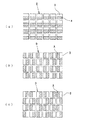
このように形成された液晶表示装置の各画素領域Dに対応する反射層の構造においては、図2(a)〜(c)に示すように、第1反射区画Aと第2反射区画Bとが縦又は横に並ぶように配置されている。第1反射区画Aと第2反射区画Bの配列方法は図2における(a)、(b)及び(c)に示すように、隣接する他の画素領域Dとの関係で種々考えられ、複数の画素領域に亘ってなるべく偏りのないような方法で決定される。図2に示す3種の配列方法はいずれも各画素領域Dを縦又は横に2分割した場合を示しているが、例えば縦に2分割した画素領域と、横に2分割した画素領域とを交互に或いは適宜分散させて配列してもよい。
【0040】
図3には、異なる態様の画素領域Dを有する液晶表示装置の構造を概念的に示す。図3(a)に示すものは、各画素領域Dの中心部に第1反射区画Aを配置し、第1反射区画Aの周囲に第2反射区画Bを配置したものである。また、図3(b)に示すものは、各画素領域D内を4分割し、第1反射区画Eと、第2反射区画Fとをそれぞれ2つずつ設けたものである。図3(c)は図3(b)と同様の第1反射区画Eと第2反射区画Fとを各画素領域Dに設けたものであるが、隣接する各画素領域Dにおける区画配置が相互に異なる場合を示したものである。
【0041】
上述のように、各画素領域D内の反射層に複数の反射区画を形成することによって、各画素領域が反射率の異なる複数の区画に分割されたこととなり、反射層の鏡面性を低減させることができるので、液晶高分子複合層7が光透過状態にある場合でも、背景が映し出されたり、直射光が目に入ったりすることが少なくなり、視認性が大幅に向上する。なお、視認性を向上させるには、複数種の反射区画をモザイク状に配列する等、パターン状に配列する場合には配列周期を細かく設定することが効果的であり、場合によってはランダムに配列してもよい。
【0042】
また、上述のようにCrとAlを用いて第1反射区画及び第2反射区画を形成した場合には、第1反射区画の反射率を50〜70%程度に、第2反射区画の反射率を90〜100%程度とすることができ、第1反射区画と第2反射区画との反射率の差を充分にとることによって、上記効果を高めることができる。その一方で、画素領域全体の反射率を両者の平均として70〜85%程度と高く維持することができるので、表示の明るさを犠牲にすることは殆どない。
【0043】
上記の実施形態では、高分子分散型の液晶表示装置の構造(図1)を例にして説明したが、同様のことは、他の光散乱や着色性を利用して、光透過状態と光散乱状態若しくは着色状態との間の状態遷移によって表示を行う液晶表示方法、例えば、コレステリック相とネマチック相との相転移を利用した相転移型表示方法、液晶の動的散乱モードを利用した方法、配向分散による表示方法等のように、偏光板を用いることのない種々の方法で表示を行う液晶表示素子及び装置に適用しても同様に効果的であり、或いはまた、その他の形式、例えば、STN液晶を用いた液晶表示装置、TN液晶を用いた液晶表示装置においても、表示品位を向上させるために適用することができる。さらに、アクティブ素子により画素電極を制御する液晶表示装置、単純マトリックス型の液晶表示装置、において本願のような構成を適用しても同様の効果を有する。
【0044】
上記の実施形態では、金属電極4の表面上に部分的に他の金属層を形成することにより反射率の異なる複数の反射区画を形成しているため、各反射区画の間の導通を容易にとることができ、また、その導通状態を安定させているが、このように重ねることなく、相互に異なる金属層を隣接して形成し、両者を直接に周縁部で導電接続し若しくは配線層を介して導電接続することによっても形成できる。なお、反射層自体は電極と兼ねる必要はなく、例えば透明電極と併設するなど、電極とは別個に設けてもよいことは明らかである。
【0045】
また、画素領域内に設ける反射区画の数や形状は任意であるが、視認性を高めるには、より多くの反射区画を複雑な形状及び配列で形成することが望ましい。さらに、反射区画を形成するための反射層の材質としては、上述のCr、Alの他に、Ag、Ni、Ta、その他の合金等の他の金属を適宜使い分けて反射率の差を設けても良く、或いは樹脂材料その他の金属以外の材料によって形成してもよい。
【0046】
なお、複数の反射区画において相互に反射率を異ならせる方法としては、反射層の材質を変える方法の他に、反射層の厚さを変える方法もある。例えば、一方の反射区画を他方の反射区画よりも厚くすることによって反射率を高めることができ、この場合、上記のように、全面に第1層を形成し、さらに一方の反射区画のみに再度第2層を形成する方法、或いは、これとは形成順を逆にした方法で、相互に異なる厚さを備えた反射区画を持つ反射層を形成することも可能である。
【0047】
さらに、反射区画における反射面の表面状態(表面粗さなど)を相互に変えることによっても、実質的な反射率を相互に変えることができる。例えば、一方の反射区画を光学的鏡面とすることによって実質的な反射率を高くし、他方の反射区画の表面を粗く形成したり、反射層表面に凹凸を形成して散乱光を増加させることによって実質的な反射率を低くすることも可能である。
【0048】
(第2実施形態)
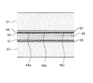
次に、本発明に係る第2実施形態について説明する。この実施形態は、図4に示すように、透明ガラスからなる基板31と基板32との間に、液晶層38を封入してなる液晶表示体である。
【0049】
基板31の内面上にはITO(インジウムスズ酸化物)等からなる例えばストライプ状の複数の透明電極33が並列するように形成されている。この電極33及び透明基板31の表面上にはポリイミド樹脂等からなる配向膜34が塗布形成される。配向膜34には所定方向にラビング処理が施される。
【0050】
一方、透明基板32の内面上には反射層を兼ねる金属電極35がCrやAl等の金属をスパッタリング法等で被着することにより形成されている。この金属電極35は例えば画素領域毎に分割された形状に形成され、それぞれが図示しない配線層に接続されている。
【0051】
この金属電極35はMIM(金属−絶縁体−金属)素子やTFT(薄膜トランジスタ)等のアクティブ素子を介して配線層に接続される場合もある。金属電極35がMIM素子を介して配線層に接続される場合には、例えば、配線層をTa、MIM素子をTa(金属)、酸化タンタル(絶縁体)、Cr(金属)の積層構造とし、金属電極35をCrで形成する。
【0052】
金属電極35の表面上には、カラーフィルタ36が形成されている。このカラーフィルタ36は、例えば以下のように形成される。まず、感光性顔料分散樹脂をスピンコート法、ロールコート法、フレキソ印刷法等により塗布し、厚さ3000〜15000Å程度に成膜する。次に、温度50〜150℃、時間5〜60分の条件でプリベークを行い、複数の色要素、例えば3原色の赤、青、緑の各着色領域36a,36b,36cを画素領域に対応させて順次形成する。この着色層に対して所望の形状のマスクを使用して露光し、現像して所望の形状にパターニングを行う。その後、温度75〜200℃、時間10〜20分の条件でポストベークを行い、各着色層を完全に硬化させる。なお、カラーフィルタの表面には図示しない保護膜が形成される。
【0053】
複数の色要素からなる各カラーフィルタ(着色領域)36a,36b,36cは、赤、青、緑の色要素からなり、それぞれ上記製法により形成された所定の平面パターンに形成されている。すなわち、各画素領域内においては、上記パターニングにより残った着色パターン部36a−1,36b−1,36c−1と、着色パターンの存在しない欠如部36a−2,36b−2,36c−2とが存在している。
【0054】
図6は本実施形態におけるカラーフィルタ36の平面パターンを示す平面図である。この図に示すように、通常は各画素領域に対応した上記着色領域の全面に着色層が形成されているが、本実施形態では、各画素領域に対応した領域の中に形成された着色層は、複数の矩形の着色パターン部36a−1,36b−1,36c−1が多数分散配置された状態にパターニングされ、その周囲が着色部の形成されていない欠如部36a−2,36b−2,36c−2となっているのである。
【0055】
本実施形態では、各画素領域内において上記平面パターンで着色層36a,36b,36cが選択的に形成されているため、透明基板31から入射した入射光が金属電極35に直接反射されて再び一方の基板31から放出される場合に、各画素領域内に形成された着色パターン部により色パターンが形成されたり屈折されたりするなど、入射光及び反射光が変調される。このことによって、液晶表示体の表示面においては、背景の映り込みや照明光の直接反射を低減する効果が得られる。
【0056】
なお、本実施形態では、カラーフィルターの色要素を、赤、青、緑の3色の色要素により構成したが、イエロー、マゼンダ、シアン、からなる3色の色要素によってカラーフィルターを構成しても良い。イエロー、マゼンダ、シアン、からなるカラーフィルターを用いた場合、カラーフィルターの透過特性が高く、反射型液晶表示装置として用いた場合、明るい表示が得られる。
【0057】
さらに、これらの3色の色要素からなるカラーフィルターに白のフィルターを用いることによって鮮明な色を表示することも可能である。
【0058】
本実施形態では、MIM素子を用いた構成であるが、TFT素子を用いて画素電極に前述のような構成を適用しても、同様な効果が得られる。更には、単純マトリックス型液晶表示装置においても同様な効果を有するものである。
【0059】
(第3実施形態)
図7は、本発明の第3実施形態におけるカラーフィルタの平面パターンを示す平面図である。この実施形態は、上記第2実施形態とほぼ同様に図4に示す縦断面構造に類似した構造を備えた液晶表示体であり、同様の部分の説明は省略し、同様の部分には同一符号を付す。
【0060】
この実施形態においては、カラーフィルタ36を構成する3色の着色領域36a,36b,36cの内部に単一の島形状に形成された着色パターン部36a−3,36b−3,36c−3が形成されている。また、これらの着色パターン部の周囲には、上記第2実施形態と同様の欠如部36a−4,36b−4,36c−4が存在する。
【0061】
本実施形態では、各着色パターン部が単一の島形状に形成されているので、パターニング工程におけるマスクパターンもそれ程微細な形状である必要がなく、精度良く、容易に形成することができる。また、マスクパターンの変更も、パターン形状はそのままで各着色領域のパターン寸法をやや小さくするだけで容易に行うことができる。
【0062】
上記第2実施形態及び第3実施形態において、各着色領域における着色パターンの寸法や形状は適宜変更することができる。この場合に、着色パターン部の着色領域全体に対する占有面積(形成面積)の割合は、望まれる着色パターンの色調によって適宜に調整することができる。また、図7に示すように、着色領域の色調の種類毎に、すなわち、上記の場合であれば、赤、青、緑の各色調毎に、表示画面上で得られる色調を最適化するためにそれぞれの面積割合を設定することができる。したがって、色調毎に上記占有面積の割合は異なることになる。このようにすると、それぞれの着色層を構成する材料自体の色調を材質や顔料濃度によって調整したり、或いは膜厚等によって調整する必要がなくなるため、色調調整が容易になり、カラーフィルタの製造工程の管理や品質管理が容易になる。
【0063】
さらに、着色領域内において着色パターンを全面的ではなく、選択的に形成していることによって、上記のように着色層のない欠如部が必ず存在し、この欠如部の存在によってカラーフィルタの下にある金属電極35から誘電体である着色層を介することなく直接に電界を液晶層38に印加することができるため、駆動電圧の低減を図ることができるとともに、駆動電圧のマージンを大きくとることも可能になる。
【0064】
本実施形態は、スイッチング素子(TFT、MIM)を使った液晶表示装置、または単純マトリックス型液晶表示装置においても適用することが可能である。
【0065】
(第4実施形態)
次に、本発明に係る第4実施形態について説明する。図5に示すように、本実施形態では、各着色領域36a’,36b’,36c’には全面的に着色層を形成しているが、この着色層には、厚肉部36a−1’,36b−1’,36c−1’と、薄肉部36a−2’,36b−2’,36c−2’とが形成されていることが特徴となっている。図8は本実施形態のカラーフィルタの平面形状を示すものである。
【0066】
このような着色層は、例えば全面的に形成した着色層に対して部分的にエッチング処理等を施すことにより表面に凹凸形状を形成したり、全面的に形成した第1層の上に、第2層を部分的に形成したり、選択的に形成した第1層の上に、第2層を全面的に形成したり、さらには、厚肉部と薄肉部とを別々に形成する等の種々の方法によって形成することができる。
【0067】
この実施形態では、着色層において部分的に厚さを異ならせることによって各着色領域内において濃淡パターンを形成し、これによって透過する光を色調的に変調することができるため、上記第2及び第3実施形態と同様に、背景の映り込みや照明による幻惑を低減し、表示品位を向上させることができる。
【0068】
この場合、着色層自体の凹凸形状或いは厚肉部及び薄肉部の形状を調整することによって、着色層を構成する材料自体の色調を変えることなく、カラーフィルタの色調を容易に調整、変更することができる。ここで、着色層の形状を調整するとは、例えば凹凸の深さ(凹部底面と凸部頂面との高低差)若しくは厚肉部と薄肉部との厚さの差、及び/又は、凹部若しくは薄肉部と凸部若しくは厚肉部の形成面積の割合を調整することである。これらは、着色層自体の平均的な厚さを変える方法よりも容易に制御することができ、精度も確保できる。
【0069】
また、上記3色の着色層の相互の色調関係を最適化するために、相互に着色層の平均厚さを調整する必要があるが、この場合にも、単にそれぞれの着色層の平均厚さを変えるのではなく、相互に凹凸形状或いは厚肉部と薄肉部の形状を変えることによって結果的に平均厚さが変わるようにすると、容易に相互間の色調関係を調整することが可能になる。
【0070】
(第5実施形態)
次に、図9を参照して本発明に係る第5実施形態について説明する。この実施形態において、上記第4実施形態と同様の部分には同一符号を付し、その説明は省略する。カラーフィルタ46は透明電極33の表面上に形成されており、カラーフィルタ46の各着色領域46a,46b,46cには、表面に第4実施形態と同様の凹凸形状が形成された着色層が形成されている。
【0071】
この実施形態に示すように、カラーフィルタは、反射層よりも表面側の位置でさえあればいかなる位置に形成されていてもよい。本実施形態においては、カラーフィルタ46に導電性を有する材料を混合させ電極33の表面に着色層を構成し、透明電極33と一体となった着色層(着色電極)を構成することが可能であり、このようにすることによって、製造工程及び構造を簡略化することができる。
【0072】
なお、上記着色層による光の変調は、結果的にカラーフィルタの各画素領域に対応する部分の内部に濃淡パターンが形成されていればよく、例えば、平面的に色調の異なる濃色部と薄色部とを分けて形成することによって構成してもよい。
【0073】
また、着色層の濃淡パターンの形成と、上記第2実施形態のような選択的な着色パターン部の形成とを適宜組み合わせることによって、最適な表示品位を得られるカラーフィルタを構成することもできる。
【0074】
上記第4実施形態及び第5実施形態に記載した構造並びに部分的に色調を変える方法によって形成した濃淡パターンのパターン形状は任意であり、例えば、第1実施形態に示した反射層の区画形状のような平面パターンに形成してもよく、また、第2実施形態又は第3実施形態の着色パターン部を一方の(すなわち濃色部又は淡色部いずれかの)パターン形状として採用してもよい。
【0075】
なお、上記各実施形態においては、特に、液晶層を高分子と液晶とが相分離した状態で互いに分離したものとした高分子分散型の液晶表示装置として形成する場合に、画面表示の明るさを確保しながら背景の映り込みを顕著に低減できるものである。これは、この種の液晶表示体においては偏光板を用いる必要がないため、本発明を適用しない場合、液晶層が光透過状態にある場合には反射層の反射光がそのまま視認され、特に背景の映り込みや照明光の反射がはっきりと現れるからである。
【0076】
高分子分散型の液晶表示装置としては、特に、液晶セル内において相溶した液晶分子及び高分子のモノマーを所定の水平方向に配向させた状態とし、高分子のモノマーを重合硬化させる、例えば光重合させて硬化させることにより、液晶分子と高分子粒子とが相互に分散された状態とするものが好ましい。この場合には、例えば、電界無印加時に液晶分子と高分子粒子の配向方向が揃って液晶高分子複合層は透明状態となり、電界印加時に液晶分子のみが電界方向に指向することによって白濁状態となる。
【0077】
上記高分子分散型の液晶表示装置の他に、偏光板を用いる必要のない液晶表示装置としては、光散乱や着色性を利用して光透過状態と光散乱状態若しくは着色状態との間の状態遷移によって表示を行う液晶表示方法、例えば、コレステリック相とネマチック相との相転移を利用した相転移型、液晶の動的散乱モードを利用したもの、配向分散によるもの等のように、種々のものがあり、これらの場合にも同様に本発明を適用することにより顕著な効果を得ることができる。
【0078】
また、アクティブ素子(MIM、TFT)を用いた液晶表示装置、単純マトリックス液晶表示装置、においても同様の効果を有するものである。
【0079】
以上説明したように、画素領域毎に反射率の異なる複数の反射区画が形成されているため、一方の基板から入射された光は、反射区画の反射率の相違によって各画素領域内においてそれぞれ変調される。
【0080】
また、液晶層が透明状態になっても、背景が映し込まれたり、直射光がそのままの状態で目に入ったりすることがなくなるから、画素領域によって形成される表示に影響を与えることなく、液晶表示装置の視認性を向上させることができる。
【0081】
また、光透過状態と光散乱状態とを制御することができ、様々な状態で表示可能となる。
【0082】
また、反射区画が裏面側電極で構成されているために、反射層を別途設ける必要がなく、電極形成工程で同時に作り込むことができる。
【0083】
また、金属その他の反射性材料の種類や組成又は形成条件を変えることにより反射率の異なる反射区画を容易に形成することができる。
【0084】
また、反射膜の厚さを部分的に変えることによって反射率を変えることができ、或いは表面に露出した材質によって部分的に反射率を変えることができるなど、積層構造によって反射率を容易に変えることができる。特に、反射層を金属電極として形成する場合には、反射区画間の相互の導通を容易かつ確実にとることができるため、電極としての機能を損なうことなく、複雑な形状の反射区画を容易に形成でき、また多数の反射区画を設けることも可能になる。
【0085】
また、カラーフィルタが画素領域内において所定の平面パターンで選択的に形成されているため、一方の基板から入射された光は、カラーフィルタを透過する際に、各画素領域内においてそれぞれカラーフィルタの形成されている部分と形成されていない部分とによって色調的に変調されるので、液晶層が透明状態になっても、背景が映し込まれたり、直射光がそのままの状態で目に入ったりすることがなくなるから、画素領域によって形成される表示に影響を与えることなく、しかも、表示の明るさを犠牲にすることなく、液晶表示装置の視認性を向上させることができる。また、カラーフィルタの形成されていない部分も存在するため、電極の電界をカラーフィルタを介することなく直接に液晶に印加することができるため、駆動電圧の低減と駆動電圧のマージンの拡大を図ることも可能である。
【0086】
また、前記液晶層は、液晶分子の中に高分子が分散した構成であり、電圧の印加状態により光透過状態と光散乱状態とを制御するため、光透過状態と光散乱状態の間で反射率を任意に制御することができる。
【0087】
また、前記カラーフィルタが赤、青、緑の色要素からなるため、フルカラー表示を得ることができる。
【0088】
また、前記カラーフィルタがイエロー、マゼンダ、シアン、の色要素から構成されているため透過率が高く、反射型表示装置として明るい表示が得られる。
【0089】
また、カラーフィルタの形成面積の割合を色要素毎に異ならせることによって、形成面積の割合によって色調を相互に調整することができ、色要素自体の色調を変えることなくカラーフィルタの色調特性を調整することができるから、高品位のカラー表示を実現することができる。
【0090】
また、カラーフィルタを単一の島状に形成することによって、例えばマスクパターンの大きさを変更するなどの軽微な変更のみで対応することができるため、従来の製造工程をほとんど変えることなく製造することができる。
【0091】
また、画素領域内に複数の分割パターン部を備えたカラーフィルタが形成されているため、入射光又は反射光を充分に変調することができ、表示品位を確実に向上させることができる。
【0092】
また、カラーフィルタが画素領域内において濃淡パターンを備えているため、この濃淡パターンによって入射光又は反射光が変調されるので、液晶層が透明状態になっても、背景が映し込まれたり、直射光がそのままの状態で目に入ったりすることがなくなるから、画素領域によって形成される表示に影響を与えることなく、しかも、表示の明るさを損なうことなく、液晶表示装置の視認性を向上させることができる。
【0093】
また、前記液晶層は、液晶分子の中に高分子が分散した構成であり、電圧の印加状態により光透過状態と光散乱状態とを制御するため、光透過状態と光散乱状態の間で反射率を任意に制御することができる。
【0094】
また、前記カラーフィルタが赤、青、緑の色要素からなるため、フルカラー表示を得ることができる。
【0095】
また、前記カラーフィルタがイエロー、マゼンダ、シアン、の色要素から構成されているため透過率が高く、反射型表示装置として明るい表示が得られる。
【0096】
また、濃淡パターンにおける濃色部と淡色部の濃度差やパターン面積の割合等を変えることによって、カラーフィルタの平均厚さを変えることができるため、色要素の色調を相互に調整することができるから、高品位のカラー表示を実現することができる。
【図面の簡単な説明】
【図1】本発明に係る液晶表示装置の第1実施形態の構造を示す断面図である。
【図2】第1実施形態における各種の画素領域の配列構造例を示す概略説明図(a)〜(c)である。
【図3】第1実施形態における各種の画素領域の配列構造例を示す概略説明図(a)〜(c)である。
【図4】本発明に係る液晶表示装置の第2実施形態の構造を示す縦断面図である。
【図5】本発明に係る液晶表示装置の第4実施形態の構造を示す縦断面図である。
【図6】本発明に係る液晶表示装置の第2実施形態のカラーフィルタの平面構造を示す平面図である。
【図7】本発明に係る液晶表示装置の第3実施形態のカラーフィルタの平面構造を示す平面図である。
【図8】本発明に係る液晶表示装置の第4実施形態のカラーフィルタの平面構造を示す平面図である。
【図9】本発明に係る液晶表示装置の第5実施形態の構造を示す縦断面図である。
【図10】従来の高分子分散型の反射型液晶表示装置の構造を示す縦断面図である。
【図11】従来のカラーフィルタを備えた反射型液晶表示装置の構造を示す縦断面図である。
【符号の説明】
1,2 透明基板
3 透明電極
4 金属電極
5,6 配向膜
7 液晶高分子複合層
7A 液晶
7B 高分子
A,E 第1反射区画
B,F 第2反射区画
D 画素領域
36,36’,46 カラーフィルタ
36a,36b,36c 着色領域
36a−1,36b−1,36c−1 着色パターン部
36a−1’,36b−1’,36c−1’ 厚肉部
36a−2’,36b−2’,36c−2’ 薄肉部[0001]
BACKGROUND OF THE INVENTION
The present invention relates to a reflective liquid crystal display device, and more particularly to a technique for improving the visibility by improving a display mode caused by reflected light.
[0002]
[Prior art]
Conventionally, as a liquid crystal display device, there are various types of devices such as a TN (twisted nematic) type liquid crystal display element, a STN (super twisted nematic) type liquid crystal display element, and a ferroelectric liquid crystal display element. Among these, the one that switches the display using the change of the polarization state of light based on the electric field effect of the liquid crystal by using the polarizing plate, and the phase change and alignment state of the liquid crystal without using the polarizing plate. In some cases, the light transmission state and the light scattering state can be switched by a change in the light intensity and other changes.
[0003]
Since the latter liquid crystal display device does not use a polarizing plate, there is an advantage that light utilization efficiency is high and a bright display can be obtained. The display characteristics in this case are substantially determined by the transparency in the light transmission state and the scattering intensity or reflectance in the light scattering state.
[0004]
As an example of a liquid crystal display device that does not use a conventionally used polarizing plate, there is a polymer dispersion type liquid crystal display device shown in FIG. In this apparatus, an
[0005]
The
[0006]
In the state where no voltage is applied between the
[0007]
Various structures and manufacturing methods of the polymer dispersion type liquid crystal display device as described above are described in detail in US Pat. No. 3600060, Japanese Patent Laid-Open No. 5-119302, and the like.
[0008]
On the other hand, some liquid crystal display devices have color filters formed to enable color display. As a liquid crystal display device capable of such color display, for example, there is one having a cross-sectional structure shown in FIG. This liquid crystal display device is of a reflective type, and a
[0009]
The
[0010]
In the reflection type liquid crystal display body formed in this way, light incident from the
[0011]
In addition, in the reflective liquid crystal display device, in addition to forming a reflective layer made of metal on the inner side of the transparent substrate as described above, a reflective layer is formed on the outer side of the transparent substrate, or the substrate itself is made reflective. In some cases, it is made of the above materials.
[0012]
[Problems to be solved by the invention]
As described above, various liquid crystal display devices that perform display in various forms using liquid crystals have been developed and put into practical use. In this case, the reflective liquid crystal display device does not require a light source such as a backlight and can reduce power consumption, and thus is suitable for use in portable devices and the like. On the other hand, in the case of the reflection type, there is a problem that the display is generally dark and it is difficult to sufficiently increase the display contrast.
[0013]
For this reason, in the reflective liquid crystal display device, it is the most important technical problem to improve the brightness and contrast of display, and various developments have been made to solve this technical problem. Has been done. A display element of a type that performs display by light scattering described above is one of the results of the development, and a display element that exhibits a bright display and good contrast can be manufactured.
[0014]
However, when the brightness and contrast of the display are improved in the reflective liquid crystal display device, there is a problem that the light reflected by the metal electrode impairs the visibility of the display. This is because the reflective layer formed by metal electrodes etc. to improve the brightness and contrast of the display is formed so as to exhibit high reflectance almost like a mirror, so the transparency of the liquid crystal layer in the light transmission state If the height is high, the surrounding scenery may be reflected on the display screen, or the direct light emitted from the illumination may enter the eyes of the user and be dazzled.
[0015]
The visibility of such a reflective liquid crystal display device is slightly improved by attaching a non-glare plate or other filters, but these filters may reduce the brightness of the display or reduce the contrast. However, the basic characteristics of the display quality such as the reflection of the background cannot be changed, and it has been difficult to significantly improve the visibility.
[0016]
In addition, in the case of the display element using the above-described light scattering, the improvement of ensuring the brightness of the display and improving the contrast by improving the transmittance in the light transmitting state has been made. There is a problem that the more the image is displayed, the more the background reflection and the dazzle by direct light become more prominent.
[0017]
Therefore, the present invention solves the above-described problems, and an object thereof is to provide a novel technique for preventing a decrease in visibility due to light reflection of a reflective layer in a reflective liquid crystal display element.
[0018]
[Means for Solving the Problems]
In order to solve the above-mentioned problem, the means taken by the present invention includes a liquid crystal layer sandwiched between a pair of substrates having electrodes on opposite inner surfaces, and a reflective layer on the side of the one substrate facing the liquid crystal layer. A plurality of pixel regions are configured by the opposing electrodes, and the liquid crystal layer has a high reflectance for each pixel region Reflection Compartment and low reflectivity Reflection And the reflectance is high. Reflection The compartment is an optical mirror and the reflectance is low Reflection The partition is characterized by being formed with irregularities.
[0019]
According to this means, since a plurality of reflection sections having different reflectivities are formed for each pixel area, light incident from one substrate is modulated in each pixel area by the difference in reflectivity of the reflection sections. Therefore, even if the liquid crystal layer becomes transparent, the background is not reflected and direct light does not enter the eyes as it is, which affects the display formed by the pixel area. In addition, the visibility of the liquid crystal display device can be improved.
[0020]
Here, the optical characteristic between the light transmission state and the light scattering state is controlled by the application state of the voltage applied to the liquid crystal layer. The plurality of reflection sections are preferably formed as back-side electrodes for applying a potential to the liquid crystal layer. In this case, since the reflection section is composed of the back surface side electrode, it is not necessary to separately provide a reflection layer, and it can be simultaneously formed in the electrode forming step.
[0021]
High reflectivity Reflection Compartment and low Reflection The partition may be formed to include different types of materials, or may be formed with different film thicknesses.
[0022]
By changing the type or composition of metal or other reflective material or the formation conditions, it is possible to easily form reflective sections having different reflectivities.
[0023]
Next, as another means, a liquid crystal is sandwiched between a pair of substrates having electrodes on opposite inner surfaces, the one substrate is provided with a reflective layer, and the reflective layer is disposed on the other substrate side. A color filter composed of a plurality of formed color elements is arranged, a plurality of pixel regions are constituted by the opposed electrodes, and the liquid crystal layer is controlled by an application state of a voltage applied to the liquid crystal layer, The color filter is formed corresponding to the pixel region, and the color filter is selectively formed in a predetermined plane pattern in the pixel region.
[0024]
According to this means, since the color filter is selectively formed in a predetermined planar pattern in the pixel region, the light incident from one substrate passes through the color filter in each pixel region. Each color filter is modulated in tone by the portion where the color filter is formed and the portion where the color filter is not formed, so even if the liquid crystal layer becomes transparent, the background is reflected or the direct light remains as it is. Therefore, the visibility of the liquid crystal display device can be improved without affecting the display formed by the pixel region and without sacrificing the brightness of the display. In addition, since there is a portion where the color filter is not formed, the electric field of the electrode can be directly applied to the liquid crystal without going through the color filter, so that the drive voltage is reduced and the drive voltage margin is increased. Is also possible.
[0025]
Here, the liquid crystal layer has a structure in which a polymer is dispersed in liquid crystal molecules, and the light transmission state and the light scattering state are controlled by applying a voltage. Further, the color filter is composed of red, blue, and green color elements, or yellow, magenta, and cyan color elements. It is preferable that the ratio of the formation area of the color filter in the pixel region is different for at least two of the color elements. According to this means, by changing the ratio of the formation area of the color filter for each color element, it is possible to mutually adjust the color tone according to the ratio of the formation area, and without changing the color tone of the color element itself. Since the color tone characteristics can be adjusted, high-quality color display can be realized.
[0026]
The planar pattern of the color filter is preferably formed in a single island shape in the pixel region. In this case, the color filter is formed in a single island shape, so it can be handled with only minor changes such as changing the size of the mask pattern. can do.
[0027]
Furthermore, it is preferable that the planar pattern of the color filter is composed of a plurality of divided pattern portions distributed in the pixel region. According to this means, since the color filter having a plurality of divided pattern portions is formed in the pixel region, incident light or reflected light can be sufficiently modulated, and display quality can be improved reliably. it can.
[0028]
Next, as another means, a liquid crystal is sandwiched between a pair of substrates having electrodes on opposite inner surfaces, the one substrate is provided with a reflective layer, and the other substrate side with respect to the reflective layer A plurality of color filters formed of a plurality of color elements are arranged, a plurality of pixel regions are formed by the opposing electrodes, and the liquid crystal layer is controlled by the application state of a voltage applied to the liquid crystal layer. The color filter is formed so as to correspond to the pixel area, and the color filter has a gray pattern having a predetermined dark area and a light area in the pixel area.
[0029]
According to this means, since the color filter has a shading pattern in the pixel region, incident light or reflected light is modulated by the shading pattern, so that the background is reflected even when the liquid crystal layer becomes transparent. The LCD display device can be viewed without affecting the display formed by the pixel area and without impairing the display brightness. Can be improved.
[0030]
Here, the liquid crystal layer has a configuration in which a polymer is dispersed in liquid crystal molecules, and the light transmission state and the light scattering state are controlled by applying a voltage. The color filter is composed of red, blue, and green color elements, or yellow, magenta, and cyan color elements.
[0031]
Further, the shading pattern may be formed by partially changing the thickness of the color filter or by partially changing the color tone of the color filter.
[0032]
Furthermore, it is preferable that the density pattern of the color filter in the pixel region is different for at least two of the color elements. According to this means, the average thickness of the color filter can be changed by changing the density difference between the dark and light color portions in the light and shade pattern, the ratio of the pattern area, etc., so the color tone of the color elements can be adjusted mutually. Therefore, high-quality color display can be realized.
[0033]
Each of the above-mentioned means is, for example, a liquid crystal polymer composite layer in which the liquid crystal layer is a liquid crystal polymer composite layer formed by compatibilizing a liquid crystal and a polymer and phase-separating the liquid crystal and the polymer. It can be applied to a liquid crystal display device.
[0034]
DETAILED DESCRIPTION OF THE INVENTION
Next, an embodiment of a liquid crystal display device according to the present invention will be described with reference to the accompanying drawings.
[0035]
(First embodiment)
FIG. 1 shows the structure of a liquid crystal cell of a liquid crystal display device according to a first embodiment of the present invention. Similar to the display device of FIG. 10 described above, the
[0036]
As in the conventional example, the liquid crystal polymer composite layer 7 becomes transparent and becomes transparent when the refractive indexes of the
[0037]
The
[0038]
In the liquid crystal display device formed as described above, the first reflection section A in which incident light is reflected by the
[0039]
In the structure of the reflective layer corresponding to each pixel region D of the liquid crystal display device formed in this way, as shown in FIGS. 2A to 2C, the first reflective section A and the second reflective section B Are arranged vertically or horizontally. As shown in FIGS. 2A, 2B, and 2C, various arrangement methods of the first reflection section A and the second reflection section B can be considered in relation to other adjacent pixel regions D. It is determined in such a way that it is as biased as possible over the pixel area. Each of the three arrangement methods shown in FIG. 2 shows a case where each pixel region D is divided into two vertically or horizontally. For example, a pixel region divided into two vertically and a pixel region divided into two horizontally are divided. They may be arranged alternately or dispersed appropriately.
[0040]
FIG. 3 conceptually shows the structure of a liquid crystal display device having pixel regions D of different modes. In FIG. 3A, the first reflection section A is disposed at the center of each pixel region D, and the second reflection section B is disposed around the first reflection section A. Also, what is shown in FIG. 3B is one in which each pixel region D is divided into four, and two each of the first reflection section E and the second reflection section F are provided. FIG. 3C is a diagram in which the first reflection section E and the second reflection section F, which are the same as those in FIG. 3B, are provided in each pixel region D. Are different cases.
[0041]
As described above, by forming a plurality of reflection sections in the reflection layer in each pixel area D, each pixel area is divided into a plurality of sections having different reflectivities, thereby reducing the specularity of the reflection layer. Therefore, even when the liquid crystal polymer composite layer 7 is in a light transmitting state, the background is not projected and direct light is less likely to enter the eyes, and the visibility is greatly improved. In order to improve visibility, it is effective to set the arrangement period finely when arranging in a pattern, such as arranging multiple types of reflection sections in a mosaic pattern, and in some cases randomly arranging May be.
[0042]
Further, when the first reflection section and the second reflection section are formed using Cr and Al as described above, the reflectance of the second reflection section is set to about 50 to 70%. 90 to 100%, and the above effect can be enhanced by sufficiently taking the difference in reflectance between the first reflection section and the second reflection section. On the other hand, since the reflectance of the entire pixel region can be maintained as high as about 70 to 85% as an average of both, the brightness of display is hardly sacrificed.
[0043]
In the above embodiment, the structure of the polymer dispersion type liquid crystal display device (FIG. 1) has been described as an example. However, the same thing can be obtained by utilizing other light scattering and coloring properties. Liquid crystal display method for displaying by a state transition between a scattering state or a colored state, for example, a phase transition type display method using a phase transition between a cholesteric phase and a nematic phase, a method using a dynamic scattering mode of liquid crystal, The present invention is equally effective when applied to liquid crystal display elements and devices that perform display by various methods that do not use a polarizing plate, such as a display method by orientation dispersion, or other forms, for example, The liquid crystal display device using STN liquid crystal and the liquid crystal display device using TN liquid crystal can also be applied to improve display quality. Further, the same effects can be obtained even when the configuration as in the present application is applied to a liquid crystal display device in which pixel electrodes are controlled by active elements, or a simple matrix type liquid crystal display device.
[0044]
In the above-described embodiment, a plurality of reflective sections having different reflectivities are formed by partially forming another metal layer on the surface of the
[0045]
Further, the number and shape of the reflection sections provided in the pixel region are arbitrary, but it is desirable to form more reflection sections with a complicated shape and arrangement in order to improve visibility. Further, as the material of the reflective layer for forming the reflective section, in addition to the above-mentioned Cr and Al, other metals such as Ag, Ni, Ta, and other alloys are properly used to provide a difference in reflectance. Alternatively, it may be formed of a resin material or other material other than metal.
[0046]
In addition, as a method of making the reflectance different from each other in the plurality of reflective sections, there is a method of changing the thickness of the reflective layer in addition to a method of changing the material of the reflective layer. For example, the reflectance can be increased by making one reflection section thicker than the other reflection section. In this case, as described above, the first layer is formed on the entire surface, and only one reflection section is again formed. It is also possible to form a reflective layer having reflective sections having different thicknesses by a method of forming the second layer or a method in which the order of formation is reversed.
[0047]
Furthermore, the substantial reflectance can be changed mutually by changing the surface state (surface roughness, etc.) of the reflecting surface in the reflecting section. For example, by making one reflective section an optical mirror surface, the substantial reflectivity is increased, and the surface of the other reflective section is roughened, or unevenness is formed on the surface of the reflective layer to increase scattered light. Thus, the substantial reflectance can be lowered.
[0048]
(Second Embodiment)
Next, a second embodiment according to the present invention will be described. As shown in FIG. 4, this embodiment is a liquid crystal display body in which a
[0049]
On the inner surface of the
[0050]
On the other hand, a
[0051]
The
[0052]
A
[0053]
Each color filter (colored region) 36a, 36b, 36c made up of a plurality of color elements is made up of red, blue, and green color elements, and is formed in a predetermined plane pattern formed by the above-described manufacturing method. That is, in each pixel region, the
[0054]
FIG. 6 is a plan view showing a planar pattern of the
[0055]
In the present embodiment, since the
[0056]
In this embodiment, the color filter color elements are composed of three color elements of red, blue, and green. However, the color filter is composed of three color elements of yellow, magenta, and cyan. Also good. When a color filter composed of yellow, magenta, and cyan is used, the color filter has high transmission characteristics, and when used as a reflective liquid crystal display device, a bright display can be obtained.
[0057]
Further, a clear color can be displayed by using a white filter as a color filter composed of these three color elements.
[0058]
In this embodiment, the MIM element is used. However, the same effect can be obtained even if the above-described structure is applied to the pixel electrode using the TFT element. Further, a simple matrix type liquid crystal display device has the same effect.
[0059]
(Third embodiment)
FIG. 7 is a plan view showing a planar pattern of the color filter in the third embodiment of the present invention. This embodiment is a liquid crystal display body having a structure similar to the longitudinal sectional structure shown in FIG. 4 in substantially the same manner as the second embodiment, and the description of the same parts is omitted, and the same reference numerals are used for the same parts. Is attached.
[0060]
In this embodiment,
[0061]
In the present embodiment, since each colored pattern portion is formed in a single island shape, the mask pattern in the patterning process does not need to be so fine and can be easily formed with high accuracy. Further, the mask pattern can be easily changed by simply reducing the pattern size of each colored region while keeping the pattern shape as it is.
[0062]
In the said 2nd Embodiment and 3rd Embodiment, the dimension and shape of the coloring pattern in each coloring area | region can be changed suitably. In this case, the ratio of the occupied area (formation area) to the entire colored region of the colored pattern portion can be appropriately adjusted depending on the color tone of the desired colored pattern. Further, as shown in FIG. 7, in order to optimize the color tone obtained on the display screen for each color tone type of the colored region, that is, in the above case, for each color tone of red, blue, and green. Each area ratio can be set. Accordingly, the ratio of the occupied area differs for each color tone. In this way, it is not necessary to adjust the color tone of the material constituting each colored layer according to the material and the pigment concentration, or to adjust the film thickness according to the film thickness. Management and quality control become easier.
[0063]
Furthermore, since the colored pattern is selectively formed in the colored region instead of the entire surface, there is always a missing portion without a colored layer as described above, and the presence of this missing portion causes the presence of the missing portion below the color filter. Since an electric field can be directly applied to the
[0064]
This embodiment can also be applied to a liquid crystal display device using a switching element (TFT, MIM) or a simple matrix type liquid crystal display device.
[0065]
(Fourth embodiment)
Next, a fourth embodiment according to the present invention will be described. As shown in FIG. 5, in this embodiment, a colored layer is entirely formed in each
[0066]
Such a colored layer is formed by, for example, partially etching the colored layer formed on the entire surface to form an uneven shape on the surface, or on the first layer formed on the entire surface. The two layers are partially formed, the second layer is entirely formed on the selectively formed first layer, and the thick part and the thin part are separately formed. It can be formed by various methods.
[0067]
In this embodiment, a thickness pattern is partially changed in the colored layer to form a light and dark pattern in each colored region, whereby the transmitted light can be modulated in tone, so that the second and second described above can be used. As in the third embodiment, background reflection and dazzling due to illumination can be reduced, and display quality can be improved.
[0068]
In this case, it is possible to easily adjust and change the color tone of the color filter without changing the color tone of the material constituting the colored layer by adjusting the uneven shape of the colored layer itself or the shape of the thick and thin portions. Can do. Here, adjusting the shape of the colored layer means, for example, the depth of the unevenness (the difference in height between the bottom surface of the concave portion and the top surface of the convex portion), the difference in thickness between the thick portion and the thin portion, and / or the concave portion or It is to adjust the ratio of the formation area of the thin part and the convex part or the thick part. These can be controlled more easily than the method of changing the average thickness of the colored layer itself, and the accuracy can be secured.
[0069]
In addition, in order to optimize the mutual color tone relationship among the three colored layers, it is necessary to adjust the average thickness of the colored layers. In this case, too, the average thickness of each colored layer is simply used. If the average thickness changes as a result by changing the uneven shape or the shape of the thick and thin portions instead of changing the shape, it is possible to easily adjust the color relationship between each other. .
[0070]
(Fifth embodiment)
Next, a fifth embodiment according to the present invention will be described with reference to FIG. In this embodiment, the same parts as those in the fourth embodiment are denoted by the same reference numerals, and the description thereof is omitted. The
[0071]
As shown in this embodiment, the color filter may be formed at any position as long as it is located on the surface side of the reflective layer. In the present embodiment, the
[0072]
Note that the light modulation by the colored layer may result in a light / dark pattern being formed inside the portion corresponding to each pixel area of the color filter. You may comprise by forming a color part separately.
[0073]
In addition, a color filter capable of obtaining an optimum display quality can be configured by appropriately combining the formation of the shade pattern of the colored layer and the formation of the selective colored pattern portion as in the second embodiment.
[0074]
The pattern shape of the shading pattern formed by the structure described in the fourth embodiment and the fifth embodiment and the method of partially changing the color tone is arbitrary. For example, the partition shape of the reflective layer shown in the first embodiment It may be formed in such a plane pattern, and the colored pattern portion of the second embodiment or the third embodiment may be adopted as one pattern shape (that is, either the dark color portion or the light color portion).
[0075]
In each of the above embodiments, particularly when the liquid crystal layer is formed as a polymer dispersion type liquid crystal display device in which the polymer and the liquid crystal are separated from each other in a phase separated state, the brightness of the screen display is increased. It is possible to remarkably reduce the reflection of the background while ensuring the image quality. This is because, in this type of liquid crystal display, it is not necessary to use a polarizing plate. Therefore, when the present invention is not applied, when the liquid crystal layer is in a light transmitting state, the reflected light of the reflective layer is visually recognized as it is, especially in the background. This is because the reflection of light and the reflection of illumination light appear clearly.
[0076]
As a polymer-dispersed liquid crystal display device, in particular, liquid crystal molecules and polymer monomers that are compatible in a liquid crystal cell are aligned in a predetermined horizontal direction, and polymer monomers are polymerized and cured, for example, light It is preferable that liquid crystal molecules and polymer particles are dispersed in each other by polymerization and curing. In this case, for example, when no electric field is applied, the alignment directions of the liquid crystal molecules and the polymer particles are aligned and the liquid crystal polymer composite layer is in a transparent state, and when the electric field is applied, only the liquid crystal molecules are directed in the electric field direction. Become.
[0077]
In addition to the above-described polymer dispersion type liquid crystal display device, as a liquid crystal display device that does not require the use of a polarizing plate, a state between a light transmission state and a light scattering state or a colored state utilizing light scattering and colorability Various liquid crystal display methods that display by transition, such as phase transition type using phase transition between cholesteric phase and nematic phase, one using liquid crystal dynamic scattering mode, one using alignment dispersion, etc. In these cases, a remarkable effect can be obtained by similarly applying the present invention.
[0078]
In addition, a liquid crystal display device using active elements (MIM, TFT) and a simple matrix liquid crystal display device have the same effect.
[0079]
As described above, since a plurality of reflection sections having different reflectivities are formed for each pixel area, light incident from one substrate is modulated in each pixel area by the difference in reflectivity of the reflection sections. Is done.
[0080]
In addition, even if the liquid crystal layer becomes transparent, the background is not reflected, and direct light does not enter the eye as it is, without affecting the display formed by the pixel region, The visibility of the liquid crystal display device can be improved.
[0081]
Further, the light transmission state and the light scattering state can be controlled, and display can be performed in various states.
[0082]
Further, since the reflective section is composed of the back surface side electrode, it is not necessary to provide a reflective layer separately, and it can be simultaneously formed in the electrode forming step.
[0083]
In addition, it is possible to easily form reflective sections having different reflectivities by changing the type, composition, or formation condition of the metal or other reflective material.
[0084]
In addition, the reflectance can be changed by changing the thickness of the reflective film, or the reflectance can be changed depending on the material exposed on the surface. be able to. In particular, when the reflective layer is formed as a metal electrode, mutual conduction between the reflective sections can be easily and surely made, so that it is possible to easily form a reflective section having a complicated shape without impairing the function as an electrode. It can also be formed and it is possible to provide a large number of reflective sections.
[0085]
In addition, since the color filter is selectively formed in a predetermined plane pattern in the pixel region, light incident from one substrate passes through the color filter, and the color filter in each pixel region. Since it is modulated in color by the part that is formed and the part that is not formed, even if the liquid crystal layer becomes transparent, the background is reflected, or direct light enters the eye as it is Therefore, the visibility of the liquid crystal display device can be improved without affecting the display formed by the pixel region and without sacrificing the brightness of the display. In addition, since there is a portion where the color filter is not formed, the electric field of the electrode can be directly applied to the liquid crystal without going through the color filter, so that the drive voltage is reduced and the drive voltage margin is increased. Is also possible.
[0086]
In addition, the liquid crystal layer has a structure in which a polymer is dispersed in liquid crystal molecules, and the light transmission state and the light scattering state are controlled by applying a voltage. Therefore, the liquid crystal layer reflects between the light transmission state and the light scattering state. The rate can be controlled arbitrarily.
[0087]
Further, since the color filter is composed of red, blue, and green color elements, a full color display can be obtained.
[0088]
Further, since the color filter is composed of color elements of yellow, magenta, and cyan, the transmittance is high, and a bright display can be obtained as a reflective display device.
[0089]
In addition, by changing the ratio of the color filter formation area for each color element, the color tone can be mutually adjusted according to the ratio of the formation area, and the color tone characteristics of the color filter can be adjusted without changing the color tone of the color element itself. Therefore, high-quality color display can be realized.
[0090]
In addition, by forming the color filter in a single island shape, it can be handled with only minor changes such as changing the size of the mask pattern, so that it can be manufactured with almost no change in the conventional manufacturing process. it can.
[0091]
In addition, since a color filter including a plurality of divided pattern portions is formed in the pixel region, incident light or reflected light can be sufficiently modulated, and display quality can be improved reliably.
[0092]
In addition, since the color filter has a light and shade pattern in the pixel region, incident light or reflected light is modulated by this light and shade pattern, so that even if the liquid crystal layer becomes transparent, the background is reflected or is directly irradiated. Since the light does not enter the eyes as it is, the visibility of the liquid crystal display device is improved without affecting the display formed by the pixel region and without impairing the brightness of the display. be able to.
[0093]
In addition, the liquid crystal layer has a structure in which a polymer is dispersed in liquid crystal molecules, and the light transmission state and the light scattering state are controlled by applying a voltage. Therefore, the liquid crystal layer reflects between the light transmission state and the light scattering state. The rate can be controlled arbitrarily.
[0094]
Further, since the color filter is composed of red, blue, and green color elements, a full color display can be obtained.
[0095]
Further, since the color filter is composed of color elements of yellow, magenta, and cyan, the transmittance is high, and a bright display can be obtained as a reflective display device.
[0096]
In addition, since the average thickness of the color filter can be changed by changing the density difference between the dark color portion and the light color portion in the light and shade pattern, the ratio of the pattern area, and the like, the color tone of the color elements can be mutually adjusted. Therefore, high-quality color display can be realized.
[Brief description of the drawings]
FIG. 1 is a cross-sectional view showing a structure of a liquid crystal display device according to a first embodiment of the present invention.
FIGS. 2A to 2C are schematic explanatory views (a) to (c) illustrating an example of an arrangement structure of various pixel regions in the first embodiment. FIGS.
FIGS. 3A to 3C are schematic explanatory views (a) to (c) illustrating an example of an arrangement structure of various pixel regions in the first embodiment. FIGS.
FIG. 4 is a longitudinal sectional view showing the structure of a liquid crystal display device according to a second embodiment of the invention.
FIG. 5 is a longitudinal sectional view showing the structure of a fourth embodiment of a liquid crystal display device according to the present invention.
FIG. 6 is a plan view showing a planar structure of a color filter of a second embodiment of the liquid crystal display device according to the present invention.
FIG. 7 is a plan view showing a planar structure of a color filter of a third embodiment of the liquid crystal display device according to the present invention.
FIG. 8 is a plan view showing a planar structure of a color filter of a fourth embodiment of the liquid crystal display device according to the present invention.
FIG. 9 is a longitudinal sectional view showing a structure of a liquid crystal display device according to a fifth embodiment of the invention.
FIG. 10 is a longitudinal sectional view showing the structure of a conventional polymer-dispersed reflective liquid crystal display device.
FIG. 11 is a longitudinal sectional view showing a structure of a reflection type liquid crystal display device provided with a conventional color filter.
[Explanation of symbols]
1, 2 Transparent substrate
3 Transparent electrodes
4 Metal electrodes
5,6 Alignment film
7 Liquid crystal polymer composite layer
7A liquid crystal
7B polymer
A, E 1st reflection section
B, F Second reflection section
D Pixel area
36, 36 ', 46 Color filter
36a, 36b, 36c Colored area
36a-1, 36b-1, 36c-1 Colored pattern portion
36a-1 ′, 36b-1 ′, 36c-1 ′ Thick part
36a-2 ′, 36b-2 ′, 36c-2 ′ Thin portion
Claims (5)
対向する前記電極によって複数の画素領域が構成され、
前記液晶層には、前記画素領域毎に、反射率が高い反射区画と、反射率が低い反射区画とが形成され、
前記反射率が高い反射区画は光学的鏡面であり、前記反射率が低い反射区画は凹凸が形成されてなることを特徴とする反射型液晶表示装置。A liquid crystal layer is sandwiched between a pair of substrates having electrodes on opposing inner surfaces, and a reflective layer is provided on the side of the one substrate facing the liquid crystal layer,
A plurality of pixel regions are configured by the opposing electrodes,
In the liquid crystal layer, for each pixel region, a reflective section having a high reflectance and a reflective section having a low reflectance are formed,
The reflective liquid crystal display device according to claim 1, wherein the reflective section having a high reflectance is an optical mirror surface, and the reflective section having the low reflectance is formed with irregularities.
Priority Applications (1)
| Application Number | Priority Date | Filing Date | Title |
|---|---|---|---|
| JP29897696A JP3666528B2 (en) | 1995-11-10 | 1996-11-11 | Reflective liquid crystal display |
Applications Claiming Priority (5)
| Application Number | Priority Date | Filing Date | Title |
|---|---|---|---|
| JP29282295 | 1995-11-10 | ||
| JP7-292822 | 1995-11-10 | ||
| JP10531096 | 1996-04-25 | ||
| JP8-105310 | 1996-04-25 | ||
| JP29897696A JP3666528B2 (en) | 1995-11-10 | 1996-11-11 | Reflective liquid crystal display |
Related Child Applications (4)
| Application Number | Title | Priority Date | Filing Date |
|---|---|---|---|
| JP2003007624A Division JP2003228064A (en) | 1995-11-10 | 2003-01-15 | Liquid crystal display |
| JP2003007626A Division JP3666598B2 (en) | 1995-11-10 | 2003-01-15 | Liquid crystal display |
| JP2003007627A Division JP3666599B2 (en) | 1995-11-10 | 2003-01-15 | Liquid crystal display device and method for manufacturing liquid crystal display device |
| JP2003007625A Division JP3666597B2 (en) | 1995-11-10 | 2003-01-15 | Liquid crystal display |
Publications (2)
| Publication Number | Publication Date |
|---|---|
| JPH1010528A JPH1010528A (en) | 1998-01-16 |
| JP3666528B2 true JP3666528B2 (en) | 2005-06-29 |
Family
ID=27310453
Family Applications (1)
| Application Number | Title | Priority Date | Filing Date |
|---|---|---|---|
| JP29897696A Expired - Lifetime JP3666528B2 (en) | 1995-11-10 | 1996-11-11 | Reflective liquid crystal display |
Country Status (1)
| Country | Link |
|---|---|
| JP (1) | JP3666528B2 (en) |
Families Citing this family (7)
| Publication number | Priority date | Publication date | Assignee | Title |
|---|---|---|---|---|
| US6624860B1 (en) | 1998-01-26 | 2003-09-23 | Sharp Kabushiki Kaisha | Color filter layer providing transmitted light with improved brightness and display device using same |
| JP3506978B2 (en) | 1998-11-27 | 2004-03-15 | シャープ株式会社 | Reflective liquid crystal display |
| JP3674584B2 (en) | 2001-12-27 | 2005-07-20 | セイコーエプソン株式会社 | Liquid crystal display device and electronic apparatus provided with the liquid crystal display device |
| JP3972857B2 (en) * | 2003-04-25 | 2007-09-05 | ソニー株式会社 | Liquid crystal display |
| JP4604511B2 (en) * | 2004-02-26 | 2011-01-05 | カシオ計算機株式会社 | Liquid crystal display device |
| CN103221849B (en) * | 2010-11-19 | 2016-07-06 | Jsr株式会社 | The manufacture method of color filter, display element and color filter |
| WO2019064570A1 (en) * | 2017-09-29 | 2019-04-04 | 堺ディスプレイプロダクト株式会社 | Liquid crystal display device and method for manufacturing same |
-
1996
- 1996-11-11 JP JP29897696A patent/JP3666528B2/en not_active Expired - Lifetime
Also Published As
| Publication number | Publication date |
|---|---|
| JPH1010528A (en) | 1998-01-16 |
Similar Documents
| Publication | Publication Date | Title |
|---|---|---|
| JP3575024B2 (en) | Reflective color liquid crystal device and electronic equipment using the same | |
| JP4057871B2 (en) | Liquid crystal display | |
| US7616277B2 (en) | Transflective LCD device having dual thickness color filter | |
| JPH10161110A (en) | Reflection type liquid crystal display element | |
| US6933994B1 (en) | Liquid crystal display including an anisotropic scattering layer | |
| KR100385691B1 (en) | Reflection liquid crystal display element | |
| KR100306648B1 (en) | Reflective liquid crystal display device | |
| JP3666528B2 (en) | Reflective liquid crystal display | |
| JP2005128571A (en) | Color liquid crystal device and electronic apparatus using same | |
| US20020089479A1 (en) | Liquid crystal display device | |
| US6297863B1 (en) | Reflective liquid crystal display device | |
| JP4123294B2 (en) | Liquid crystal display | |
| JP3900189B2 (en) | Liquid crystal display device and method of manufacturing liquid crystal display device | |
| JP3666599B2 (en) | Liquid crystal display device and method for manufacturing liquid crystal display device | |
| JP3666598B2 (en) | Liquid crystal display | |
| JP3046730B2 (en) | Reflective diffuser and reflective liquid crystal display | |
| JP3666597B2 (en) | Liquid crystal display | |
| JP3894217B2 (en) | Liquid crystal display | |
| JP3931904B2 (en) | Method for manufacturing liquid crystal display device and liquid crystal display device | |
| JP3407641B2 (en) | Liquid crystal devices and electronic equipment | |
| TW200530679A (en) | Liquid crystal display device and electronic equipment | |
| KR100904520B1 (en) | CF substrate for LCD and methode for fabricating the same | |
| JP2003228064A (en) | Liquid crystal display | |
| JP3405340B2 (en) | Liquid crystal display device | |
| JP3606312B2 (en) | Reflective liquid crystal device and electronic apparatus using the same |
Legal Events
| Date | Code | Title | Description |
|---|---|---|---|
| RD02 | Notification of acceptance of power of attorney |
Free format text: JAPANESE INTERMEDIATE CODE: A7422 Effective date: 20040512 |
|
| A977 | Report on retrieval |
Free format text: JAPANESE INTERMEDIATE CODE: A971007 Effective date: 20040527 |
|
| A521 | Written amendment |
Free format text: JAPANESE INTERMEDIATE CODE: A523 Effective date: 20040621 |
|
| A131 | Notification of reasons for refusal |
Free format text: JAPANESE INTERMEDIATE CODE: A131 Effective date: 20040706 |
|
| A521 | Written amendment |
Free format text: JAPANESE INTERMEDIATE CODE: A523 Effective date: 20040827 |
|
| A02 | Decision of refusal |
Free format text: JAPANESE INTERMEDIATE CODE: A02 Effective date: 20041214 |
|
| A521 | Written amendment |
Free format text: JAPANESE INTERMEDIATE CODE: A523 Effective date: 20050209 |
|
| A911 | Transfer of reconsideration by examiner before appeal (zenchi) |
Free format text: JAPANESE INTERMEDIATE CODE: A911 Effective date: 20050223 |
|
| TRDD | Decision of grant or rejection written | ||
| A01 | Written decision to grant a patent or to grant a registration (utility model) |
Free format text: JAPANESE INTERMEDIATE CODE: A01 Effective date: 20050316 |
|
| A61 | First payment of annual fees (during grant procedure) |
Free format text: JAPANESE INTERMEDIATE CODE: A61 Effective date: 20050329 |
|
| R150 | Certificate of patent or registration of utility model |
Free format text: JAPANESE INTERMEDIATE CODE: R150 |
|
| FPAY | Renewal fee payment (event date is renewal date of database) |
Free format text: PAYMENT UNTIL: 20080415 Year of fee payment: 3 |
|
| FPAY | Renewal fee payment (event date is renewal date of database) |
Free format text: PAYMENT UNTIL: 20090415 Year of fee payment: 4 |
|
| FPAY | Renewal fee payment (event date is renewal date of database) |
Free format text: PAYMENT UNTIL: 20090415 Year of fee payment: 4 |
|
| FPAY | Renewal fee payment (event date is renewal date of database) |
Free format text: PAYMENT UNTIL: 20100415 Year of fee payment: 5 |
|
| FPAY | Renewal fee payment (event date is renewal date of database) |
Free format text: PAYMENT UNTIL: 20110415 Year of fee payment: 6 |
|
| FPAY | Renewal fee payment (event date is renewal date of database) |
Free format text: PAYMENT UNTIL: 20110415 Year of fee payment: 6 |
|
| FPAY | Renewal fee payment (event date is renewal date of database) |
Free format text: PAYMENT UNTIL: 20120415 Year of fee payment: 7 |
|
| FPAY | Renewal fee payment (event date is renewal date of database) |
Free format text: PAYMENT UNTIL: 20130415 Year of fee payment: 8 |
|
| FPAY | Renewal fee payment (event date is renewal date of database) |
Free format text: PAYMENT UNTIL: 20130415 Year of fee payment: 8 |
|
| FPAY | Renewal fee payment (event date is renewal date of database) |
Free format text: PAYMENT UNTIL: 20140415 Year of fee payment: 9 |
|
| S531 | Written request for registration of change of domicile |
Free format text: JAPANESE INTERMEDIATE CODE: R313531 |
|
| R350 | Written notification of registration of transfer |
Free format text: JAPANESE INTERMEDIATE CODE: R350 |
|
| EXPY | Cancellation because of completion of term |