JP3661193B2 - Liquid crystal device and driving method thereof, and projection display device and electronic apparatus using the same - Google Patents
Liquid crystal device and driving method thereof, and projection display device and electronic apparatus using the same Download PDFInfo
- Publication number
- JP3661193B2 JP3661193B2 JP51817498A JP51817498A JP3661193B2 JP 3661193 B2 JP3661193 B2 JP 3661193B2 JP 51817498 A JP51817498 A JP 51817498A JP 51817498 A JP51817498 A JP 51817498A JP 3661193 B2 JP3661193 B2 JP 3661193B2
- Authority
- JP
- Japan
- Prior art keywords
- period
- data signal
- precharge
- horizontal scanning
- liquid crystal
- Prior art date
- Legal status (The legal status is an assumption and is not a legal conclusion. Google has not performed a legal analysis and makes no representation as to the accuracy of the status listed.)
- Expired - Fee Related
Links
Images


Classifications
-
- G—PHYSICS
- G09—EDUCATION; CRYPTOGRAPHY; DISPLAY; ADVERTISING; SEALS
- G09G—ARRANGEMENTS OR CIRCUITS FOR CONTROL OF INDICATING DEVICES USING STATIC MEANS TO PRESENT VARIABLE INFORMATION
- G09G3/00—Control arrangements or circuits, of interest only in connection with visual indicators other than cathode-ray tubes
- G09G3/20—Control arrangements or circuits, of interest only in connection with visual indicators other than cathode-ray tubes for presentation of an assembly of a number of characters, e.g. a page, by composing the assembly by combination of individual elements arranged in a matrix no fixed position being assigned to or needed to be assigned to the individual characters or partial characters
- G09G3/34—Control arrangements or circuits, of interest only in connection with visual indicators other than cathode-ray tubes for presentation of an assembly of a number of characters, e.g. a page, by composing the assembly by combination of individual elements arranged in a matrix no fixed position being assigned to or needed to be assigned to the individual characters or partial characters by control of light from an independent source
- G09G3/36—Control arrangements or circuits, of interest only in connection with visual indicators other than cathode-ray tubes for presentation of an assembly of a number of characters, e.g. a page, by composing the assembly by combination of individual elements arranged in a matrix no fixed position being assigned to or needed to be assigned to the individual characters or partial characters by control of light from an independent source using liquid crystals
- G09G3/3611—Control of matrices with row and column drivers
- G09G3/3648—Control of matrices with row and column drivers using an active matrix
-
- G—PHYSICS
- G09—EDUCATION; CRYPTOGRAPHY; DISPLAY; ADVERTISING; SEALS
- G09G—ARRANGEMENTS OR CIRCUITS FOR CONTROL OF INDICATING DEVICES USING STATIC MEANS TO PRESENT VARIABLE INFORMATION
- G09G2310/00—Command of the display device
- G09G2310/02—Addressing, scanning or driving the display screen or processing steps related thereto
- G09G2310/0243—Details of the generation of driving signals
- G09G2310/0248—Precharge or discharge of column electrodes before or after applying exact column voltages
-
- G—PHYSICS
- G09—EDUCATION; CRYPTOGRAPHY; DISPLAY; ADVERTISING; SEALS
- G09G—ARRANGEMENTS OR CIRCUITS FOR CONTROL OF INDICATING DEVICES USING STATIC MEANS TO PRESENT VARIABLE INFORMATION
- G09G2320/00—Control of display operating conditions
- G09G2320/02—Improving the quality of display appearance
- G09G2320/0223—Compensation for problems related to R-C delay and attenuation in electrodes of matrix panels, e.g. in gate electrodes or on-substrate video signal electrodes
-
- G—PHYSICS
- G09—EDUCATION; CRYPTOGRAPHY; DISPLAY; ADVERTISING; SEALS
- G09G—ARRANGEMENTS OR CIRCUITS FOR CONTROL OF INDICATING DEVICES USING STATIC MEANS TO PRESENT VARIABLE INFORMATION
- G09G2340/00—Aspects of display data processing
- G09G2340/02—Handling of images in compressed format, e.g. JPEG, MPEG
-
- G—PHYSICS
- G09—EDUCATION; CRYPTOGRAPHY; DISPLAY; ADVERTISING; SEALS
- G09G—ARRANGEMENTS OR CIRCUITS FOR CONTROL OF INDICATING DEVICES USING STATIC MEANS TO PRESENT VARIABLE INFORMATION
- G09G3/00—Control arrangements or circuits, of interest only in connection with visual indicators other than cathode-ray tubes
- G09G3/001—Control arrangements or circuits, of interest only in connection with visual indicators other than cathode-ray tubes using specific devices not provided for in groups G09G3/02 - G09G3/36, e.g. using an intermediate record carrier such as a film slide; Projection systems; Display of non-alphanumerical information, solely or in combination with alphanumerical information, e.g. digital display on projected diapositive as background
-
- G—PHYSICS
- G09—EDUCATION; CRYPTOGRAPHY; DISPLAY; ADVERTISING; SEALS
- G09G—ARRANGEMENTS OR CIRCUITS FOR CONTROL OF INDICATING DEVICES USING STATIC MEANS TO PRESENT VARIABLE INFORMATION
- G09G3/00—Control arrangements or circuits, of interest only in connection with visual indicators other than cathode-ray tubes
- G09G3/20—Control arrangements or circuits, of interest only in connection with visual indicators other than cathode-ray tubes for presentation of an assembly of a number of characters, e.g. a page, by composing the assembly by combination of individual elements arranged in a matrix no fixed position being assigned to or needed to be assigned to the individual characters or partial characters
- G09G3/34—Control arrangements or circuits, of interest only in connection with visual indicators other than cathode-ray tubes for presentation of an assembly of a number of characters, e.g. a page, by composing the assembly by combination of individual elements arranged in a matrix no fixed position being assigned to or needed to be assigned to the individual characters or partial characters by control of light from an independent source
- G09G3/36—Control arrangements or circuits, of interest only in connection with visual indicators other than cathode-ray tubes for presentation of an assembly of a number of characters, e.g. a page, by composing the assembly by combination of individual elements arranged in a matrix no fixed position being assigned to or needed to be assigned to the individual characters or partial characters by control of light from an independent source using liquid crystals
- G09G3/3611—Control of matrices with row and column drivers
- G09G3/3614—Control of polarity reversal in general
Landscapes
- Engineering & Computer Science (AREA)
- Chemical & Material Sciences (AREA)
- Crystallography & Structural Chemistry (AREA)
- Physics & Mathematics (AREA)
- Computer Hardware Design (AREA)
- General Physics & Mathematics (AREA)
- Theoretical Computer Science (AREA)
- Control Of Indicators Other Than Cathode Ray Tubes (AREA)
- Liquid Crystal Display Device Control (AREA)
Description
[技術分野]
本発明は、液晶装置及びその駆動方法、並びにそれを用いた投写型表示装置及び電子機器に関する。
[背景技術]
例えば、アクティブマトリクス型の液晶装置では、一走査信号線に複数接続されたTFT(薄膜トランジスタ)等のスイッチング素子を介して、各画素の液晶層にデータを書き込む動作を点順次駆動により実施している。
また、液晶にかかる電圧の偏りによる表示むらをなくし、液晶にかかる直流電流による液晶の劣化などを防ぐために、液晶に印加される電圧の極性を所定のタイミングで反転させる極性反転駆動が行われている。
極性反転駆動とは、液晶の一端に、液晶の他端に印加される電位を基準として異なる極性(正または負の極性)の電圧を印加する駆動である。尚、本明細書における「極性」とは、液晶の両端に印加される電圧の極性を意味する。極性反転駆動するには、TFTを用いたアクティブマトリクス型では、液晶を挟んで画素電極と対向する共通電極に印加する電位を変化させるか、あるいは、画素電極に印加される画像データ信号の電圧振幅の中間電位を基準として画像データ信号の電位レベルを変化させている。
ここで、前記極性反転においては、走査信号線を選択するごとに極性反転を行ういわゆるライン毎の反転、あるいはこれに、一走査信号線に接続された画素毎に極性反転を行ういわゆるドット毎の反転を組み合わせた極性反転駆動方式が知られている。
図9、図10に、極性反転駆動方式について説明するための模式図を示す。従来のアクティブマトリクス型の液晶装置では、点順次駆動でかつ画素毎(ライン毎も含む)の極性反転駆動方式を採用し、また、データ信号線のプリチャージは直前のブランキング期間に一括して行う方式を採用している。
図9、図10において、S1〜S4はデータ信号線を示し、H1〜H4は走査信号線を示している。各画素の「+」,「−」は、該画素の液晶に印加される電圧およびその直前にデータ信号線に供給されるプリチャージ電位の極性を示している。図9はNフィールドでの各画素の電圧極性を、図10はN+1フィールドでの各画素の電圧極性を示している。画素毎及びライン毎の極性反転駆動においては、同一データ信号線と接続された隣合う画素毎(図9,図10で縦方向にて隣接する画素毎)に、異なる極性にて電圧が印加されるようになっている。
この場合、同一データ信号線に接続され、かつ、異なる走査信号線に接続された隣り合う2つの画素に、表示上で例えば同じ黒データを書き込む場合でも、極性反転駆動のために各々の黒データの信号レベルは異なっている。このとき、データ信号線自体が寄生容量を持つため、データ信号線の電位を、正極性側の黒レベル電位から負極性側の黒レベル電位に変化させるのに時間を要する。
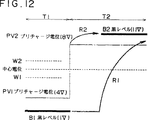
図11、図12を参照して、同一のデータ信号線に接続された隣り合う2つの画素に、それぞれ同じ黒を書き込む動作を場合のデータ信号線の電位の変化について説明する。
図11において、C10はデータ信号線S1に寄生する容量(つまり、データ信号線S1の等価容量)を示す。また、図11の左側に記載の「−」,「+」は、画素22,24に書き込まれる電圧の極性を示している。なお、画素22,24は共に「黒」を表示するものとする。画素はスイッチング素子を介してデータ信号が供給される蓄積容量及び画素電極と、画素電極と共通電極の間で電圧印加される液晶層とからなる。
図12に示すように、水平走査期間T1において、画素22の一端に黒レベル電位B1を印加して黒表示し、次の水平走査期間T2において、画素24の一端に黒レベル電位B2を印加して同様に黒表示する。この場合、画素22,24の他端には、各黒レベル電位B1,B2間に設定された共通電極電位が印加されているため、画素22には負極性の電圧が印加され、画素24には正極性の電圧が印加され、同じ黒表示でも液晶への印加電圧の極性が反転されている。しかも、上記のようなノーマリーホワイトの表示では、それぞれの黒レベル電位B1とB2との電位差が、他の階調表示の場合と比較して最も大きくなる。よって、プリチャージを行わなければ、画像データ信号自体によってデータ信号線S1の寄生容量C10を充電(あるいは放電)して、図中「R1」で示すようにデータ信号線の電位を黒レベル電位B1からB2へと変化させなければならない。
これに対し、データ信号の供給に先立ち、データ信号の極性と同じ極性のプリチャージを行っておけば、つまり、水平走査期間T2の前にプリチャージを行ってデータ信号線S1を高電位の第2のプリチャージ電位PV2に保持しておけば、図中「R2」で示すように、データ信号線の電位を第2のプリチャージ電位PV2から黒レベル電位B2へと変化させるだけで良く、データ信号線S1の寄生容量C10の充電(放電)の量が小さくて良い。ゆえに、液晶の駆動が高速化される。
ところで、従来の液晶装置においては、黒レベル電位B1,B2をそれぞれ1V,11Vとし、白レベル電位W1,W2をそれぞれ5V,7Vとし、プリチャージ電位PV1,PV2をそれぞれ4V,8Vに設定していた。すなわち、プリチャージ電位PV1,PV2は、ビデオ振幅である黒レベル電位B1,B2間の中心電位(6V)に対して対称に設定していた。
この4V,8Vは、中間調表示レベルの時に液晶の一端にスイッチング素子を介して印加される電圧であり、液晶印加電圧(V)と液晶装置の透過率(T)との関係を示すT−Vカーブが最も急峻となる時の電位レベルに相当している。換言すれば、この4V,8Vは、液晶への印加電圧の変化に対する透過率変化が最も大きい時の電位レベルに相当している。プリチャージ電位PV1,PV2をこのように設定すると、プリチャージ電位から中間調表示のための電位になるまでデータ信号線を短時間で充放電でき、サンプリング期間が短くなっても正確な中間調表示が可能となる。
ここで、前述したように、画像表示装置は、多角的に用いられるようになってきており、例えば、液晶モニタ,ノート・パソコン(PC),民生機器に用いられている。従って、高精細化,携帯性強化という観点からの開発が進められており、例えば、高精細化においては、VGA(640×480画素)からXGA(1024×768画素)、XGAからSXGA(1280×1024画素)、SXGAからUXGA(1600×1200画素)へと、画素数の多い画像表示装置の開発が進展している。
前記画像表示装置は、画像データ信号の種類により各々の動作周波数は異なっている。例えば、VGAは、ノート・パソコンのモニタとして用いられているが、この動作周波数は、60Hz,72Hz,75Hzである。そして、例えば、SVGAも、VGA用よりも大型のノート・パソコンのモニタとして用いられているが、この動作周波数は、56Hz,60Hz,72Hz,75Hzである。更に、例えば、XGAも、デスクトップ・パソコン或はノート・パソコンのモニタとして用いられているが、この動作周波数は、60Hz,70Hz,75Hzであり、また、例えば、EWS(SXGA)の動作周波数は75Hzである。
例えば、液晶装置としてVGA仕様(60Hz)の装置を使用した場合、1水平走査期間においては、800ドットクロック信号で31778μsec,有効表示期間中の画素は640クロック分を有する。従って、前記したような各駆動周波数56,60,72,75Hzをこの装置に適用する場合には、一水平走査期間が短くなる。また、ディジタル信号処理により外部入力の画像データ信号の圧縮・伸長も可能であり、このような方法にて各画像データ信号に対応した画像表示を行うことができる。
また、このような液晶装置は、プロジェクタ等に適用されており、この場合は、各画像データ信号の種類を切り換えても、適宜画像データ信号の圧縮・伸長を行うことによって、画像表示を行うことができる構成になっている。
このような画像表示装置における画素数の増加に伴い、液晶パネルの大型化が進展し、それに伴って画像表示装置における画像むらが目立つようになってきており、画素やバックライトの均一性を向上し、輝度むらや色むらを低減するという手法により、前記画像むらに対処している。
ところが、画素数の増加に伴う高周波数化に対しては、様々な工夫がなされているものの、液晶装置においては各スイッチ素子がTFTにて構成されている。よって、データ信号のサンプリングだけでなく、プリチャージにおいてもスイッチング特性が低速であるという問題があり、それに伴う種々の回路動作について検討がなされている。
また、走査信号線においては、X方向における画素数分のスイッチング素子としてのTFTのゲートが各々接続されているので、走査信号線においては、容量成分が大きくなってしまう。また、パネルサイズの大型化に伴い走査信号線の配線抵抗も増加する。よって、走査信号線における寄生抵抗や寄生容量が大きくなって、負荷となることに起因する配線遅延の問題が生じている。
本発明は、前記問題点を鑑みてなされたものであり、本発明の目的は、プリチャージ信号の供給経路における寄生容量,寄生抵抗及びスイッチング素子における寄生容量,寄生抵抗による負荷に起因した、スイッチング時の信号伝搬速度の遅延による画質の低下を防止することができる液晶装置、液晶駆動方法、それを用いた投写型表示装置及び電子機器を提供することにある。
本発明の他の目的は、走査信号線における寄生容量,寄生抵抗及びスイッチング素子における寄生容量,寄生抵抗による負荷に起因した、スイッチング時の信号伝搬速度の遅延による画質の低下を防止することができる液晶装置、液晶駆動方法、それを用いた投写型表示装置及び電子機器を提供することにある。
本発明のさらに他の目的は、データ信号線駆動手段(Xドライバ)の起動時を基準としてプリチャージ及びサンプリングのタイミングを設定することで、異なる種類の画像データ信号を前記液晶装置に供給しても、画像が劣化することのない液晶装置、液晶駆動方法、それを用いた投写型表示装置及び電子機器を提供することにある。
[発明の開示]
本発明の一態様によれば、
複数のデータ信号線と複数の走査信号線の交差により形成される複数の画素の各々に、画素に接続されたスイッチング素子を配置してなり、前記画素に印加される電圧の極性を所定期間ごとに反転させて駆動する液晶装置において、
前記複数の走査信号線の少なくとも1本に接続された複数のスイッチング素子を水平走査期間にオンさせる水平走査信号を、前記複数の走査信号線に順次供給する走査側駆動手段と、
前記複数のデータ信号線の各々にそれぞれ接続され、サンプリング期間にデータ信号を順次サンプリングし前記複数のデータ信号線の各々に供給する複数のサンプリング用スイッチング手段と、
前記複数のサンプリング用スイッチング手段に前記サンプリング期間を設定する信号を供給するデータ側駆動手段と、
前記複数のデータ信号線の各々に前記データ信号を順次供給する前記サンプリング期間に先立つプリチャージ期間に、当該データ信号に基づいて前記画素の液晶層に印加される電圧の極性と同一極性のプリチャージ電圧にて、前記複数のデータ信号線の各々を同時にプリチャージする複数のプリチャージ用スイッチング手段と、を有し、
同一水平走査期間内における前記プリチャージ期間終了から先頭の前記サンプリング用スイッチング手段の前記サンプリング期間が開始される迄の時間間隔を、前記データ信号線に接続された前記プリチャージ用スイッチング手段での信号伝搬遅延時間よりも長く設定したことを特徴とする。
本発明の一態様によれば、予め設計されたプリチャージ期間終了後に、複数のプリチャージ用スイッチング手段の各々にて信号伝搬遅延時間が生じたとしても、画質の劣化を低減できる。すなわち、全てのプリチャージ用スイッチング手段がオフした後に、複数のデータ信号線の各々に対するデータサンプリングが開始されるからである。これにより、特に水平走査期間にて最初にサンプリング期間が開始されるデータ信号線においても、それに接続されたプリチャージ用スイッチング手段及びサンプリング用スイッチング手段の双方が同時にオンする事態を防止できる。これにより、データ信号線に書き込まれたデータ信号電位がプリチャージ電位の悪影響をうけることがなくなり、該データ信号線に接続された画素での階調値が変動することがない。
プリチャージ期間終了から水平走査期間での先頭のサンプリング期間が開始される迄の時間間隔は、プリチャージ用スイッチング手段がそれぞれ有する負荷に基づく各時定数の和よりも大きく設定されることが好ましい。こうすると、上記時間間隔は、プリチャージ用スイッチング手段での信号伝搬遅延時間よりも長くなる。
データ側駆動手段は、該データ側駆動手段を起動させるシフトデータ信号がアクティブとなった後に、サンプリング信号を出力する構成とすることができる。この場合、前記信号伝搬遅延時間より長い前記時間間隔を、プリチャージ期間終了からシフトデータ信号がアクティブとなる迄の時間とすればよい。
本発明では、プリチャージ期間終了から水平走査期間での先頭のサンプリング期間が開始される迄の時間間隔を調整設定する調整回路を含むことができる。
この調整回路は、基準クロック信号をカウントし、水平同期信号にてリセットされるカウンタと、前記カウンタの出力をデコードして、前記時間間隔を設定する信号を出力するデコーダと、前記デコーダの出力に基づいて、前記プリチャージ信号及び前記シフトデータ信号を生成する信号生成回路とを有する。この調整回路により、上記時間間隔だけ隔ててプリチャージ信号及びシフトデータ信号を生成できる。
また、この調整回路は、駆動周波数に拘らず前記時間間隔を一定とすることができる。従って、駆動周波数の異なる各種の画像データ信号が供給されても、常に画質を低下することがない。
本発明の他の態様によれば、
複数のデータ信号線と複数の走査信号線の交差により形成される複数の画素の各々に、画素に接続されたスイッチング素子を配置してなり、前記画素に印加される電圧の極性を所定期間ごとに反転させて駆動する液晶装置において、
前記複数の走査信号線の少なくとも1本に接続された複数のスイッチング素子を水平走査期間にオンさせる水平走査信号を、前記複数の走査信号線に順次供給する少なくとも一つの走査側駆動手段と、
前記複数のデータ信号線の各々にそれぞれ接続され、サンプリング期間にデータ信号を順次サンプリングし前記複数のデータ信号線の各々に供給する複数のサンプリング用スイッチング手段と、
前記複数のサンプリング用スイッチング手段に前記サンプリング期間を設定する信号を供給するデータ側駆動手段と、
前記複数のデータ信号線の各々に前記データ信号を順次供給する前記サンプリング期間に先立つプリチャージ期間に、当該データ信号に基づいて前記画素の液晶層に印加される電圧の極性と同一極性のプリチャージ電圧にて、前記複数のデータ信号線の各々を同時にプリチャージする複数のプリチャージ用スイッチング手段と、を有し、
(m−1)番目の水平走査期間の終了時から、m番目の水平走査期間内に設定されたプリチャージ期間の開始時迄の時間間隔が、前記少なくとも一つの走査側駆動手段から最も遠い位置の画素に至る水平走査信号の信号伝搬遅延時間よりも長く設定されたものであることを特徴とする。
本発明の他の態様は、走査側駆動手段から最も遠い位置の画素に至る水平走査信号の信号伝搬遅延時間が最も長いことに着目して、該画素での画質の劣化を防止したものである。液晶装置では、予め設計された(m−1)番目の水平走査期間が終了しても、その後上記信号伝搬遅延時間に基づいて(m−1)番目の実質の水平走査期間が延長される。本発明では、最も長い信号伝搬遅延時間経過後に、m番目の水平走査期間でのプリチャージ期間が開始される。従って、(m−1)番目の水平走査期間にオンされた複数のスイッチング素子に接続された画素が、m番目の水平走査期間のためのプリチャージ電位の悪影響を受けることがなくなる。
(m−1)番目の水平走査期間の終了時からm番目の水平走査期間内に設定されたプリチャージ期間の開始時迄の時間間隔は、1本の前記走査信号線及び前記最も遠い画素のスイッチング素子がそれぞれ有する負荷に基づく各時定数の和よりも大きく設定されることが好ましい。こうすると、上記時間間隔を、走査側駆動手段から最も遠い位置の画素に至る水平走査信号の信号伝搬遅延時間よりも長くできる。
本発明では、(m−1)番目の水平走査期間の終了時からm番目の水平走査期間内に設定されたプリチャージ期間の開始時迄の時間間隔を調整設定する調整回路を含むことができる。
この調整回路は、基準クロック信号をカウントし、水平同期信号にてリセットされるカウンタと、前記カウンタの出力をデコードして、前記時間間隔を設定する信号を出力するデコーダと、前記デコーダの出力に基づいて、前記プリチャージ信号及び前記シフトデータ信号を生成する信号生成回路とを有する。この調整回路により、(m−1)番目の水平走査期間の終了時より上記時間間隔だけ隔てて、m番目の水平走査期間のプリチャージ信号を生成できる。
また、この調整回路は、駆動周波数に拘らず前記時間間隔を一定とすることができる。従って、駆動周波数の異なる各種の画像データ信号が供給されても、常に画質を低下することがない。
上述した各発明では、前記液晶が封入された一対の基板を有し、前記複数のサンプリング用スイッチング手段を、前記一対の基板の一方に形成された複数のスイッチング素子にて形成することができる。このようなスイッチング素子は、MOSトランジスタまたは薄膜トランジスタにて形成できる。
また、本発明を、上述した特徴を有する液晶装置を備えた投写型表示装置あるいは電子機器に適用すると、それらにて表示される画質の劣化を防止できる。
【図面の簡単な説明】
図1は、本発明のアクティブマトリクス型液晶装置におけるプリチャージ動作及びデータサンプリング動作を説明するためのタイミングチャートである。
図2は、本発明の実施の形態1に係るアクティブマトリクス型液晶装置の概略図である。
図3は、本発明の実施の形態1に係るアクティブマトリクス型液晶装置のプリチャージスイッチ及びサンプリングスイッチを説明するための図である。
図4は、本発明の実施の形態1に係るアクティブマトリクス型液晶装置のYドライバの動作を説明するタイミングチャートである。
図5は、先頭画素に接続されたデータ信号線の電位を説明するためのタイミングチャートである。
図6は、末端画素に接続されたデータ信号線の電位を説明するためのタイミングチャートである。
図7は、図2のタイミング回路ブロック内に設けられる調整回路のブロック図である。
図8は、各種のビデオソースを説明するための概略説明図である。
図9は、Nフィールドでの極性反転動作を説明するための概略説明図である。
図10は、N+1フィールドでの極性反転動作を説明するための概略説明図である。
図11は、1本のデータ信号線に接続された相隣接する2つの画素を説明するための概略説明図である。
図12は、図11に示す2つの画素にてそれぞれ黒表示するときのデータ信号線の電位を説明するための概略説明図である。
図13は、先頭画素に接続されたデータ信号線の電位変動を説明するためのタイミングチャートである。
図14は、画質の劣化が生ずる領域を説明するための概略説明図である。
図15は、末端画素に接続されたデータ信号線の電位変動を説明するためのタイミングチャートである。
図16は、走査信号線の両端にそれぞれYドライバを有する装置を示す概略説明図である。
図17は、本発明による液晶装置を用いて構成される電子機器の概略図である。
図18は、本発明が適用される液晶プロジェクタの概略図である。
図19は、本発明が適用されるパーソナルコンピュータ(PC)の概略図である。
[発明を実施するための最良の形態]
<実施の形態1>
(装置の概略構成)
図2に、実施の形態1に係る液晶装置の全体概要が示されている。同図に示すように、この液晶装置は、電子機器、例えば液晶プロジェクタのライトバルブとして用いる小型液晶装置であり、液晶パネルブロック10と、タイミング回路ブロック20と、データ処理回路ブロック30とに大別される。
タイミング回路ブロック20は、ドットクロック信号CLK,水平同期信号HSYNC,垂直同期信号VSYNCに基づいて、Xドライバのシフトクロック信号CLX*,Yドライバのシフトクロック信号CLY*,Xドライバのシフト信号DX,Y側シフトデータ信号DY等、所定のタイミング信号を生成・出力するものである。このタイミング回路ブロック20は、後述するプリチャージタイミング信号Pのパルス幅を設定するパルス可変機能を有している。
データ処理回路ブロック30は、液晶表示に適するようにデータの増幅,反転等によりデータを処理する回路ブロックである。そして、前記データ処理回路ブロック30において、一画素ごとに外部入力される画像データ信号Dataを、極性反転基準電位を基準として極性反転することにより、データ信号を生成している。
液晶パネルブロック10は、一対の基板間に液晶が封入され、一方の基板上に画素領域100と、Yドライバ102と、Xドライバ104、サンプリングスイッチ106と、プリチャージ用スイッチ172を備え、これと対向する他方の基板上に共通電極を備えて構成される。一対の液晶パネル基板の外側には偏光板が配置される。なお、これらの駆動回路は、液晶パネル基板とは分離して、外付けICとして構成しても良い。
画素領域100上には、例えば、図2の行方向に沿って延びる複数の走査信号線110と、例えば、列方向に沿って延びる複数のデータ信号線112とが形成されている。尚、本実施の形態では、便宜上、走査信号線110の総数を492本とし、データ信号線112の総数を652本として説明するが、前記走査信号線及びデータ信号線の本数は特に限定されず、画素数の多い液晶装置ほどその効果は大きくなる。
この各走査信号線110,各データ信号線112が交差する各位置には、スイッチング素子114と画素120とが直列に接続されて表示要素が構成されている。各画素120は、一方の基板上に共に形成される、スイッチング素子114と接続される画素電極、及び各画素電極と隣接する走査信号線や容量線との間に形成される蓄積容量117と、対向する他方の基板状に形成される共通電極と、両電極の間に挟持される液晶層116とから構成される。
各画素120のスイッチング素子114がオンする期間を選択期間と称し、オフする期間を非選択期間と称する。選択期間にスイッチング素子114を介して画素120に供給された電圧を非選択期間にて蓄積する蓄積容量117が、液晶層116に接続されている。
本実施の形態では、スイッチング素子114を、例えば、3端子型スイッチング素子としており、例えばTFT(薄膜トランジスタ)にて構成している。これに限らず、他の3端子型スイッチング素子であるMOSトランジスタ、あるいは2端子型スイッチング素子例えば、MIM(金属−絶縁−金属)素子、MIS(金属−絶縁−半導体)素子などを用いることができる。なお、本実施の形態の画素領域100は、2端子型または3端子型のスイッチングを用いたアクティブマトリクス型の液晶表示パネルに限らず、単純マトリクス型の液晶表示パネルなど、他の種々の液晶パネルであってもよい。
Yドライバ102は、シフトレジスタと論理回路により構成され、シフトレジスタには前記タイミング回路ブロック20にて生成されたY側シフトデータ信号DY及びY側シフトクロック信号CLY*が入力され、複数の走査信号線110a,110b,…の中から少なくとも1本の走査信号線110を順次選択するための選択期間が設定された水平走査信号h1,h2,h3,…を出力するものである(図4参照)。
このYドライバ102のシフトレジスタは、走査信号線110の本数に相当する段数を有するとともに、各々隣り合うシフトレジスタ段同士が接続されており、Y側シフトデータ信号DYの伝送が順次行われている。
シフトレジスタの各段からは、図4に示すY側シフトレジスタ出力信号Y1,Y2,Y3,…が出力される。そして、Y側シフトレジスタ出力信号Y1,Y2の論理積演算により水平走査信号h1を生成する。同様に、隣合う2つのY側シフトレジスタ段の出力Yn,Yn+1の論理積演算により、水平走査信号h2,h3,…を生成する。
よって、これら水平走査信号h1,h2,h3…は、Y側シフトデータ信号DYが入力された後に出力される。
Xドライバ104は、前記タイミング回路ブロック20にて生成されたX側シフトクロック信号CLX*とX側シフトデータ信号DXとが入力され、データ処理回路ブロック30の出力線である例えば1本の信号ラインと、画素領域100のデータ信号線112a,112b,・・・との間に配置された複数のサンプルホールドスイッチ106に対して、画素領域100を点順次駆動するためのサンプリング信号S1,S2,S3,…を出力するものである。
このXドライバ104もYドライバ102と同様に、複数のデータ信号線の本数分に相当する段数を有するシフトレジスタ含むとともに、各々隣り合うシフトレジスタ段同士が接続されており、前記X側シフトデータ信号DXの伝送が順次行われている。
このXドライバ104も図4のタイミングチャートと同様に動作し、図1に示すように、シフトデータ信号DXが入力された後に、サンプリング信号SH1,SH2,・・・を生成するものである。
なお、データ処理回路ブロック30が、公知の相展開回路を有する場合には、データ処理回路ブロック30の出力線は、その相展開数と同じ本数の出力線となる。従って、Xドライバ104は、その複数本のデータ出力線よりそれぞれデータをサンプリングするためのサンプリング信号を出力することになる。ここで、相展開回路とは、シリアルデータとしての画像データ信号を、基準クロックに基づいて設定されたサンプリング期間に従ってサンプルホールドし、かつ、一定の画素毎に前記シリアルデータを展開して、1データ出力期間が基準クロックの整数倍に変換された複数のデータ信号をパラレル出力するものである。
プリチャージ用スイッチ172a,172b,・・・を所定のタイミングにてオンさせて、第1(負極性)のプリチャージ電源供給用ライン174aまたは第2(正極性)のプリチャージ電源供給用ライン174bを、各データ信号線112a,112b・・・に接続して、データ信号線112をプリチャージするためのものである。
この第1,第2プリチャージ電源供給ライン174a,174bには、プリチャージ電源供給用スイッチ190を介して第1のプリチャージ電位PV1,第2のプリチャージ電位PV2が、走査信号線110を選択するごと(一水平走査ごと)に切り換えられて供給される。なお、電源供給用スイッチ190の切り換えタイミングは、少なくともプリチャージ用スイッチ172のオンする前に設定される。
本実施の形態では、極性反転駆動を実施することから、例えば奇数番目の水平走査期間では、奇数番目のデータ信号線172a,172c,・・・は第1のプリチャージ電源供給ライン174aに接続され、偶数番目のデータ信号線172b、172d,・・・は第2のプリチャージ電源供給ライン174bに接続される。また、偶数番目の水平走査期間では、奇数番目のデータ信号線172a,172c,・・・は第2のプリチャージ電源供給用ライン174bに接続され、偶数番目のデータ信号線172b,172d,・・・は第1のプリチャージ電源供給用ライン174bに接続される。なお、このプリチャージ動作の詳細については後述する。
すなわち、本実施の形態では、走査信号線の延びる方向での1画素ごとに極性反転駆動し、かつ、データ信号線の延びる方向で1ラインごと(一走査信号線毎)に極性反転駆動しており、これに合うように極性反転タイミングが定められている。なお、プリチャージが必要な場合とは、少なくとも1ラインごとに極性反転駆動しているものであり、1画素毎の極性反転に限定されるものではない。
実施の形態1の液晶装置では、図1に示すブランキング期間(帰線期間)TBに設定されたプリチャージ期間T2内にて、その後のサンプリング期間h1,h2,h3,…にてサンプリングされるデータ信号に基づき画素に印加される電圧の極性と同一極性で、各々のデータ信号線をプリチャージしている。
本実施の形態においては、データ信号のサンプリングを確実に行うため、データ信号のサンプリング期間h1,h2,h3,…を、プリチャージ用スイッチが完全にオフされた後に開始させている。しかも、m−1番目の水平走査期間の全ての画素のスイッチング素子が完全にオフされた後に、m番目の水平走査期間のプリチャージ期間を開始させている。
このために、図1に示すプリチャージ期間T2の終了からX側シフトデータ信号DXがオンするまでの時間T1と、前回の水平走査期間の終了から次回の水平走査期間内のプリチャージ期間の開始までの時間T3とを、下記にて説明する第1,第2の課題を解決するように設定している。
(プリチャージに関する第1の課題)
図13は、水平走査信号hmと、m番目の水平走査期間のプリチャージ信号PCと、1本目のデータ信号線にデータ信号電位を供給するためのサンプリング信号S1と、そのデータ信号S1のデータ信号電位を示している。なお、図13ではX側シフトデータ信号DXを省略している。この水平走査信号hmは、図3に示すm本目の走査信号線110に接続された全ての画素のスイッチング素子114のゲートに印加されて、そのスイッチング素子114をオン,オフさせる信号である。
この水平走査信号hmがあるハイとなった後に、プリチャージ信号PCがハイとなる。このプリチャージ信号PCが全てのプリチャージスイッチ172のゲートに印加される際には、図13の破線で示すように、波形になまりが生ずる。
図13に示すように波形になまりが生じた場合、本来のプリチャージ期間が終了したにも拘わらず、プリチャージスイッチ172のゲートには、スイッチのTFTのしきい値電圧Vthを越える電圧がさらに期間t1だけ印加され続ける。このとき、m本目の走査信号線Hmに接続された画素のうち、図3に示す水平走査方向の先頭画素(m,1)にデータ信号電位を書き込むためのサンプリング信号S1が最初にオンする。これにより、データ信号線S1に接続されたサンプリングスイッチ106がオンする。もし、図13に示すように、期間t1中にデータ信号線S1に接続されたプリチャージスイッチ172とサンプリングスイッチ106が同時にオンすると、データ信号線S1の電位は図13の実線に示すとおり変動する。
ここで、プリチャージ前のデータ信号線S1の電位を、画素にて負極性電圧にて黒表示するための電位(1V)に設定されたものと仮定する。図13に示すように、m番目の水平走査期間にてプリチャージ信号PCがオンすることで、データ信号線S1の電位は、1Vから第2のプリチャージ電位PV2(8V)にプリチャージされる。その後、サンプリング信号S1がハイとなり、サンプリングスイッチ106を介して正極性の電圧にて白表示するためのデータ信号電位(7V)をデータ信号線S1に供給するものと仮定する。このとき、期間t1では、データ信号線S1に接続されたプリチャージスイッチ172とサンプリングスイッチ106が同時にオンしている。このため、データ信号線S1の一端は第2のプリチャージ電位PV2(8V)とされ、その他端は7Vとされ、データ信号線S1はこの両電圧の影響を受けることになる。
従って、データ信号線S1の電位は、図13の破線の通り8Vから直ちに7Vまで放電されず、両スイッチ172,106が順次オフされたときのデータ信号線S1の電位は、図13の実線の通り本来の7VよりもΔV1だけ高い電位となる。このため、画素(m,1)の画素では、第2のプリチャージ電位の影響を受けて、ノーマリホワイトの場合には本来の白表示よりも暗い表示となる。なお、画素(m,1)への書き込み電位が第2のプリチャージ電位よりも高い場合には、本来の表示よりも明るい表示に変動する。
このようなプリチャージ信号PCの波形のなまりは、下記の負荷に基づく時定数に起因して生ずる。その負荷とは、図3のデータ信号線S1に接続されたプリチャージスイッチ172と導通するプリチャージ電源供給ライン174bの有する寄生抵抗Rb,寄生容量Cb(図示せず)及びプリチャージ信号PCを供給するプリチャージ信号供給ライン173の有する寄生抵抗Rp,寄生容量Cp(図示せず)である。なお、他の奇数及び偶数番目に設けられたプリチャージスイッチ172に関しても、これと接続されたプリチャージ電源供給ライン174a,174bの有する寄生抵抗Ra,Rb及び寄生容量により完全にオンする迄に時間を浪費してしまう。また、全てのプリチャージスイッチ172は、そのゲートに対してソース・ドレインが容量結合されている。このため、図3に示すように、データ信号線S1に接続されたプリチャージスイッチ172において寄生容量C1が形成され、この負荷に基づく時定数も影響する。なお他の全てプリチャージスイッチ、例えば図3に示すx番目のプリチャージスイッチにおいても寄生容量Cxが形成されてしまう。このため、各プリチャージスイッチ172各ゲートに前記プリチャージ信号PCが入力されると、全てのプリチャージスイッチ172が完全にオフするのに時間を要してしまうので、各プリチャージスイッチ172のゲートに供給されるプリチャージ期間信号PCの信号波形がなまってしまう。
このような現象は、一括プリチャージ後にサンプリング期間が設定される水平走査方向のYドライバ近傍に配置される画素にて生じ、図14の画素先頭領域A(m−1,1)やA(m,1)にて画質が劣化する。
(プリチャージに関する第2の課題)
図15は、水平走査信号h(m−1),h(m)と、m番目の水平走査期間のプリチャージ信号PCと、図3に示すx番目のデータ信号線Sxの電位を示している。この水平走査信号h(m−1),h(m)は、図3に示すm−1本目及びm本目の走査信号線110に接続された全てのスイッチング素子114のゲートにそれぞれ印加されて、それらのスイッチング素子114をオン,オフさせる信号である。
ここで、この水平走査信号h(m−1)が図3の画素(m−1,x)のスイッチング素子114のゲートに印加される際には、図15の破線で示すように、波形になまりが生ずる。ここでは、水平走査信号(m−1)の立ち下がりの波形のなまりを問題とし、プリチャージ信号PCの波形のなまりは無視する。
図15に示すように波形になまりが生じた場合、m−1番目の本来の水平走査期間が終了し、m番目の水平走査期間が開始されたにも拘わらず、m−1本目の走査信号線Hm−1に接続された画素(m−1,x)のスイッチング素子114ゲートには、TFT114のしきい値電圧Vthを越える電圧がさらに期間t2だけ印加され続ける。この結果、画素(m−1,x)のスイッチング素子114は期間t2でも引き続きオンしており、そのスイッチング素子114のドレインに接続された画素120は、そのスイッチング素子114のソースに接続されたx本目のデータ信号線112(Sx)の電圧の影響を受け、リークする。
ここで、図15に示すように、m−1番目の水平走査期間では、データ信号線Sxに8Vのデータ信号電位が充電されて中間調表示がなされていたと仮定する。
このとき、期間t2内にてプリチャージ信号がオンすると、データ信号線Sxは、図15の破線で示すように第1のプリチャージ電位PV1(4V)にプリチャージされる。すなわち、データ信号線Sxは8Vより4Vに向けて放電され、図15ではその放電途中にてスイッチング素子114がオフされている。
このため、画素(m−1,x)の画素120の電荷がリークされ、画素120のチャージ電圧がΔV2だけ降下する。この結果、ノーマリホワイトの場合には画素(m−1,x)での表示が明るくなってしまう。逆にノーマリブラックの場合には画素(m−1,x)での表示が暗くなる。
この現象の原因である水平走査信号の波形のなまりは、下記にて説明する負荷の時定数に起因して生ずる。
この負荷とは、走査信号線110の寄生抵抗及び寄生容量である。ここで、各走査信号線110は、例えばポリシリコン層にて形成されているため、アルミニウムにて形成されているプリチャージ電源供給ライン174a,174b及びプリチャージ信号供給ライン173と比較して、寄生容量及び寄生抵抗は大きく、水平走査信号の転送はプリチャージ信号の転送よりも遅れる傾向にある。特に、Yドライバ102より離れた位置にある画素A(m−1,x)におけるスイッチング素子114のゲート電位の上昇及び下降がなまり、それ自体の寄生容量Cxにより、さらにスイッチング素子114がオン,オフするタイミングが遅れる。ここで、Yドライバ102が走査信号線110の一端に接続される場合には、水平走査信号はその他端の画素ほど転送遅れが著しい。従って、この場合には図14の領域Bでの画質が劣化する。一方、図16に示すように、Yドライバ102a,102bが走査信号線110の両端に接続されている場合には、図14の画面中央領域Cにて画質が劣化する。
つまり、プリチャージは全データ信号線112に対し一括で同時に行われているので、Yドライバ102から遠い画素ほどスイッチング素子114のオフタイミングの遅れが著しいので、上記のような画質の劣化が生ずるのである。
(改善されたプリチャージ動作)
本実施の形態発明の液晶装置のを示すタイミングチャートを図1に示し、図13に示す第1の課題を解決したタイミングチャートを図5に、図15に示す第2の課題を解決したタイミングチャートを図6に示す。
実施の形態1の液晶装置では、図1に示すブランキング期間TBに設定されたプリチャージ期間T2内にて、その後のサンプリング期間h1,h2,h3,…にてサンプリングされるデータ信号に基づき画素に印加される電圧の極性と同一極性で、各々のデータ信号線をプリチャージしている。
本実施の形態においては、図1に示す通り、m−1番目の水平走査信号h(m−1)がオンしてm−1番目の水平走査期間が開始された後、期間T3経過後にプリチャージ信号PCがハイとなって、プリチャージ期間T2が開始される。また、ブランキング期間TB内にてプリチャージ期間T2が終了した後、期間T1経過後に先頭画素のためのサンプリング信号S1がハイとなり、その後順次他のサンプリング信号S2,S3,…がハイとなる。
ここで、上述した図13に示す第1の課題を解決して先頭画素(m,1)での表示品質を向上するためには、図1及び図5に示す期間T1は、下記の式1にて示される時定数τpとの関係を、T1≧τpあるいはT4>τpに設定している。
式1;τp=α1・Rb・Cb+α2・Rp・Cp(α1,α2:定数)
上記式1にて、プリチャージ信号供給ライン173における寄生抵抗,寄生容量をRp,Cpとし、プリチャージ電源供給ライン174bにおける寄生抵抗,寄生容量をRb,Cbとしている。
T1≧τpとすると、図5に示すように、水平走査信号h(m−1)がロー、すなわち、m−1番目の走査信号線110に接続された全てのスイッチング素子114がオフとなった後に、m番目の走査信号線Hmに接続された画素へのサンプリングを開始させるX側シフトデータ信号DXがアクティブとなる。ここで、m番目の走査信号線Hmの先頭画素A(m,1)にデータ信号電位を書き込むためのサンプリング信号S1は、X側シフトデータ信号DXがアクティブとなった後にアクティブとなる。従って、図13での動作とは異なり、図5においては、データ信号線S1に接続されたサンプリングスイッチ106とプリチャージスイッチ172が同時にオンすることはない。このため、図5に示すように、第2のプリチャージ電位PV2(8V)にプリチャージされていたデータ信号線S1は、サンプリング信号S1によって規定されるサンプリング期間h1内に、本来のデータ信号電位である7Vまでに放電させることができる。
本実施の形態では、先頭画素のためのプリチャージ信号S1がアクティブとなる前に必ずX側シフトデータ信号DXがアクティブとなるため、T1≧τpとすれば必ずT4>τpを満足する結果となる。ただし、上述した第1の課題を解決するためには、T4>τpのみが成立するものでも良い。
次に、上述した図15に示す第2の課題を解決して画素A(m−1,x)での表示品質を向上するためには、図1及び図6に示す期間T3は、下記の式2にて示される時定数τhとの関係を、T1>τhに設定している。
式2;τh=β1・Rh・Ch+β2・Rx・Cx(β1,β2:定数)
式2において、走査信号線110における寄生抵抗,寄生容量をRh,Chとし、スイッチング素子TFTxにおける寄生抵抗,寄生容量をRx,Cxとしている。
こうすると、図6に示すように、水平走査信号h(m−1)に接続された全てのスイッチング素子114が完全にオフされた後に、m番目の水平走査期間のためのプリチャージ信号PCをオンすることができる。このため、Yドライバ102から最も離れた位置の画素A(m−1,x)の画素が、第1のプリチャージ電位PV1の悪影響を受けることがなくなる。
(各期間T1〜T3の設定方法)
各期間T1,T3の各期間は、前述したように、各々信号伝送時間に影響を及ぼす負荷が有する時定数τp,τhよりも大きい期間に設定している。また、期間T2は、データ信号線110を第1,第2のプリチャージ電位にプリチャージできる長さに定められる。従って、この期間T2と等しいプリチャージ信号PCのパルス幅を、ドットクロック信号CLKのカウントに基づき、適当なパルス幅に設定している。
これらの期間は、図7に示すタイミング回路ブロック20内の調整回路により設定することができる。この調整回路は、基準クロックCLKをカウントし、水平同期信号HSYNCによりリセットされるプログラマブルカウンタ20Aと、このプログラマブルカウンタ20Aからの出力に基づいて、プリチャージ信号PC及びX側シフトデータ信号DXを出力するデコーダ20Bとを有する。プログラマブルカウンタ20Aは、水平同期信号HSYNCの立ち上がりから期間T3及び期間T3+T2に対応するカウント値を出力することで、デコーダ20Bは図1に示すプリチャージ信号PCのアクティブ期間を設定するプリチャージタイミング信号Pを生成できる。また、プログラマブルカウンタ20Aは、水平同期信号HSYNCの立ち上がりから期間T3+T2+T1に対応するカウント値を出力することで、デコーダ20Bは図1に示すX側シフトデータ信号DXを生成するタイミングを決定できる。信号生成回路20Cは、デコーダ20Bからの出力に基づいて、図1に示すタイミングにてプリチャージ信号PC及びX側シフトデータ信号DXを生成する。このようにすることで、結果として、X側シフトデータ信号DXを基準として、期間T1〜T3を設定することができる。そして、上記のカウント値を可変とすることで、期間T1〜T3を所望に調整できる。なお、期間T1〜T3の調整は、カウンタ20Aのカウント値を変更するものに限らず、デコーダ20Bでのデコード解析設定を変更するものでも良い。この期間期間T1,T2,T3の最終的な調整は、液晶装置組み立て後の検査工程にて行うことができる。
このようにすることで、液晶装置の駆動周波数に拘らず、期間T1〜T3を一定の長さとすることができる。つまり、X側シフトデータ信号DXを基準として期間T1〜T3を設定することで、駆動周波数が変化しても期間T1〜T3は不変となる。
例えば、図8に示すような各駆動周波数を有する画像データ信号(ビデオソース)をもつ各液晶装置についても、X側シフトデータ信号DXを基準として常に一定の期間T1〜T3が設定されているので容易に対応することができる。ここで、図8における各液晶装置及びビデオソース(画像データ信号)の組み合わせの各図においては、数字は画素数は有効表示期間を示している。また、各装置に各ビデオソースを適用するときは必要に応じ、データ信号の圧縮・伸長を行うことでどのビデオソースを採用しても容易に各液晶駆動方法に適用することができる。例えば、VGA仕様の液晶装置に、SVGA仕様のビデオソースを適用するときは、ディジタル信号処理を行って画像データの圧縮を行うことで、前記VGA仕様の液晶装置に適合したビデオソースに変化させることができる。このデータ信号の圧縮・伸長は、ディジタル信号処理ICにより行うことができるが、これは前記データ処理回路ブロック30内に前記回路機能を持たせることも、外付けのICを使用することもどちらも可能である。
ここで、実施の形態1においては、前記第1のプリチャージ電位PV1を8V,前記第2のプリチャージ電位PV2を4Vとして説明したが、これに限定されることなく、適宜設定することが可能である。
また、本実施の形態においては、一例として、画素A(m,1),A(m−1,n+x)にてそれぞれ白表示、中間調表示を行う場合について説明したが、どのような画像表示を行う場合にも前述したような問題点を全て解決することができる。
また、本実施の形態においては、正極性側の黒レベル電位を11V,白レベル電位を7V、負極性側の黒レベル電位を1V,白レベル電位を5Vとして説明したが、特にこれに限定されることはない。
本実施の形態では、前記サンプリングスイッチは、ハイレベルのサンプリング期間信号が入力されてオン状態とされるN型のトランジスタであることを前提として説明したが、これに限定されることなく、サンプリングスイッチをP型トランジスタで構成し、ロウレベルのサンプリング期間信号を入力させるようにすることもできる。この場合は、前記Xドライバにて前記サンプルホールドスイッチとは逆の信号波形を有するサンプリング期間信号を形成することで容易に実現することができる。スイッチング素子も同様にP型トランジスタにて形成することができる。
<実施の形態2>
上述の各実施の形態の画像表示装置を用いて構成される電子機器は、図17に示す表示情報出力源1000、表示情報処理回路1002、表示駆動回路1004、液晶パネルなどの表示パネル1006、クロック発生回路1008及び電源回路1010を含んで構成される。表示情報出力源1000は、ROM、RAM、などのメモリ、テレビ信号を同調して出力する同調回路などを含んで構成され、上述のタイミング回路ブロック20に相当するクロック発生回路1008からのクロックに基づいて、ビデオ信号などの表示情報を出力する。
表示情報処理回路1002は、上述の各実施の形態のデータ処理回路ブロック30に相当し、クロック発生回路1008からのクロックに基づいて表示情報を処理して出力する。この表示情報処理回路1002は、増幅・極性反転回路、相展開回路、ローテーション回路等の他、ガンマ補正回路及びクランプ回路等を含むことができる。
駆動回路1004は、上述のYドライバ102、Xドライバ104及びプリチャージ駆動回路160、或はXドライバ104を含んで構成され、画素領域1006を表示駆動する。電源回路1010は、上述の各回路に電力を供給する。
このような構成の電子機器として、図18に示す液晶プロジェクタ、図19に示すマルチメディア対応のパーソナルコンピュータ(PC)及びエンジニアリング・ワークステーション(EWS)、ページャ、或は携帯電話、ワードプロセッサ、テレビ、ビューファインダー型またはモニタ直視型のビデオテープレコーダ、電子手帳、電子卓上計算機、カーナビゲーション装置、POS端末、タッチパネルを備えた装置などを挙げることができる。
図18に示す液晶プロジェクタは、透過型液晶パネルをライトバルブとして用いた投写型プロジェクタであり、例えば、3板プリズム方式の光学系を用いている。図18において、プロジェクタ1100では、白色光源のランプユニット1102から射出された投写光がライトガイド1104の内部で、複数のミラー1106及び2枚のダイクロイックミラー1108によってR、G、Bの3原色に分けられ、各々の色の画像を表示する3枚のアクティブマトリクス型液晶パネル1110R、1110G及び1110Bによって変調された光は、ダイクロイックプリズム1112に3方向から入射される。
ダイクロイックプリズム1112では、レッドR及びブルーBの光が90゜曲げられ、グリーンGの光が直進するので各色の画像が合成され、投写レンズ1114を通してスクリーンなどにカラー画像が投写される。
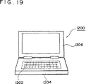
図19に示すパーソナルコンピュータ1200は、キーボード1202を備えた本体部1204と、液晶表示画面1206とを有する。
尚、本発明は上記実施の形態に限定されるものではなく、本発明の要旨の範囲内で種々の変形実施が可能である。例えば、本発明は上述の各種の液晶パネルの駆動に適用されるものに限らず、エレクトロルミネッセンス、プラズマディスプレー装置、CRT等を用いた画像表示装置にも適用可能である。
また、上記実施の形態においては、TFTをスイッチング素子として用いた例を説明したが、スイッチング素子ングはMIM等の2端子素子でも良い。この場合、走査信号線とデータ信号線との間に2端子素子と画素とが直列接続されて画素が構成されるので、両信号ラインの差電圧が画素に供給される。
また、上記実施例においては、TFTをスイッチング素子として用い、液晶パネルの素子が形成された基板をガラスや石英の基板としたが、これに代えて半導体基板を用いることもできる。この場合、TFTではなく、MOSトランジスタがスイッチング素子となる。[Technical field]
The present invention relates to a liquid crystal device, a driving method thereof, a projection display device using the same, and an electronic apparatus.
[Background technology]
For example, in an active matrix liquid crystal device, an operation of writing data to a liquid crystal layer of each pixel is performed by dot sequential driving via a switching element such as a TFT (thin film transistor) connected to a plurality of scanning signal lines. .
In addition, in order to eliminate display unevenness due to the bias of voltage applied to the liquid crystal and to prevent deterioration of the liquid crystal due to direct current applied to the liquid crystal, polarity inversion driving is performed to invert the polarity of the voltage applied to the liquid crystal at a predetermined timing. Yes.
The polarity inversion drive is a drive in which a voltage having a different polarity (positive or negative polarity) is applied to one end of the liquid crystal with reference to a potential applied to the other end of the liquid crystal. In the present specification, “polarity” means the polarity of a voltage applied to both ends of the liquid crystal. In the active matrix type using TFT for polarity inversion driving, the potential applied to the common electrode facing the pixel electrode across the liquid crystal is changed, or the voltage amplitude of the image data signal applied to the pixel electrode The potential level of the image data signal is changed with reference to the intermediate potential.
Here, in the polarity inversion, so-called line-by-line inversion that performs polarity inversion each time a scanning signal line is selected, or so-called dot-by-dot that performs polarity inversion for each pixel connected to one scanning signal line. A polarity inversion driving method combining inversion is known.
9 and 10 are schematic diagrams for explaining the polarity inversion driving method. A conventional active matrix liquid crystal device employs a dot inversion driving method and a polarity inversion driving method for each pixel (including each line), and data signal lines are precharged all at once in the immediately preceding blanking period. The method to do is adopted.
9 and 10, S1 to S4 indicate data signal lines, and H1 to H4 indicate scanning signal lines. “+” And “−” of each pixel indicate the voltage applied to the liquid crystal of the pixel and the polarity of the precharge potential supplied to the data signal line immediately before that. FIG. 9 shows the voltage polarity of each pixel in the N field, and FIG. 10 shows the voltage polarity of each pixel in the N + 1 field. In the polarity inversion driving for each pixel and each line, a voltage with a different polarity is applied to each adjacent pixel connected to the same data signal line (each pixel adjacent in the vertical direction in FIGS. 9 and 10). It has become so.
In this case, even when the same black data is written on two adjacent pixels connected to the same data signal line and connected to different scanning signal lines, for example, each black data is used for polarity inversion driving. The signal levels are different. At this time, since the data signal line itself has a parasitic capacitance, it takes time to change the potential of the data signal line from the black level potential on the positive polarity side to the black level potential on the negative polarity side.
With reference to FIG. 11 and FIG. 12, a change in the potential of the data signal line in the operation of writing the same black in two adjacent pixels connected to the same data signal line will be described.
In FIG. 11, C10 indicates a capacitance parasitic on the data signal line S1 (that is, an equivalent capacitance of the data signal line S1). Further, “−” and “+” on the left side of FIG. 11 indicate the polarities of the voltages written in the
As shown in FIG. 12, in the horizontal scanning period T1, a black level potential B1 is applied to one end of the
On the other hand, if the precharge with the same polarity as that of the data signal is performed prior to the supply of the data signal, that is, the precharge is performed before the horizontal scanning period T2, and the data signal line S1 is set to the high potential. If the precharge potential PV2 is maintained at 2, the data signal line potential need only be changed from the second precharge potential PV2 to the black level potential B2, as indicated by “R2” in the figure. The amount of charge (discharge) of the parasitic capacitance C10 of the signal line S1 may be small. Therefore, the driving speed of the liquid crystal is increased.
By the way, in the conventional liquid crystal device, the black level potentials B1 and B2 are set to 1V and 11V, the white level potentials W1 and W2 are set to 5V and 7V, respectively, and the precharge potentials PV1 and PV2 are set to 4V and 8V, respectively. It was. That is, the precharge potentials PV1 and PV2 are set symmetrically with respect to the center potential (6V) between the black level potentials B1 and B2 that are video amplitudes.
These 4V and 8V are voltages applied to one end of the liquid crystal via a switching element at the halftone display level, and T− indicates the relationship between the liquid crystal applied voltage (V) and the transmittance (T) of the liquid crystal device. This corresponds to the potential level when the V curve is the steepest. In other words, 4V and 8V correspond to the potential level when the transmittance change with respect to the change in the voltage applied to the liquid crystal is the largest. By setting the precharge potentials PV1 and PV2 in this way, the data signal lines can be charged and discharged in a short time from the precharge potential to the potential for halftone display, and accurate halftone display even when the sampling period is shortened Is possible.
Here, as described above, image display devices are used in various ways, and are used in, for example, liquid crystal monitors, notebook personal computers (PCs), and consumer devices. Therefore, development from the viewpoint of higher definition and enhanced portability is underway. For example, in higher definition, VGA (640 × 480 pixels) to XGA (1024 × 768 pixels), XGA to SXGA (1280 × Development of image display devices with a large number of pixels is progressing from 1024 pixels) to UXGA (1600 × 1200 pixels).
The image display devices have different operating frequencies depending on the type of image data signal. For example, the VGA is used as a monitor of a notebook computer, and the operating frequency is 60 Hz, 72 Hz, and 75 Hz. For example, SVGA is also used as a monitor of a notebook PC larger than that for VGA, and this operating frequency is 56 Hz, 60 Hz, 72 Hz, and 75 Hz. Furthermore, for example, XGA is also used as a monitor for desktop personal computers or notebook personal computers, but this operating frequency is 60 Hz, 70 Hz, 75 Hz, and for example, the operating frequency of EWS (SXGA) is 75 Hz. It is.
For example, when a device of VGA specification (60 Hz) is used as the liquid crystal device, in one horizontal scanning period, an 800 dot clock signal has 31778 μsec, and a pixel in an effective display period has 640 clocks. Therefore, when the drive frequencies 56, 60, 72, and 75 Hz as described above are applied to this apparatus, one horizontal scanning period is shortened. Also, it is possible to compress / decompress externally input image data signals by digital signal processing, and image display corresponding to each image data signal can be performed by such a method.
Further, such a liquid crystal device is applied to a projector or the like. In this case, even if the type of each image data signal is switched, image display is performed by appropriately compressing / decompressing the image data signal. It is configured to be able to.
Along with the increase in the number of pixels in such an image display device, the enlargement of the liquid crystal panel has progressed, and accordingly, the image unevenness in the image display device has become conspicuous, improving the uniformity of pixels and backlights. However, the image unevenness is dealt with by a technique of reducing brightness unevenness and color unevenness.
However, although various devices have been devised for increasing the frequency with the increase in the number of pixels, in the liquid crystal device, each switch element is constituted by a TFT. Therefore, there is a problem that the switching characteristic is low not only in the sampling of the data signal but also in the precharge, and various circuit operations associated therewith have been studied.
Further, in the scanning signal line, the TFT gates as switching elements corresponding to the number of pixels in the X direction are connected to each other, so that the capacitance component becomes large in the scanning signal line. In addition, the wiring resistance of the scanning signal line increases as the panel size increases. Therefore, the parasitic resistance and parasitic capacitance in the scanning signal line are increased, causing a problem of wiring delay due to the load.
The present invention has been made in view of the above-mentioned problems, and an object of the present invention is to perform switching caused by a parasitic capacitance and a parasitic resistance in a precharge signal supply path and a parasitic capacitance in the switching element and a load caused by the parasitic resistance. An object of the present invention is to provide a liquid crystal device, a liquid crystal driving method, a projection display device using the same, and an electronic apparatus that can prevent deterioration in image quality due to a delay in signal propagation speed.
Another object of the present invention is to prevent deterioration in image quality due to a delay in signal propagation speed at the time of switching due to parasitic capacitance and parasitic resistance in the scanning signal line, and parasitic capacitance in the switching element and load due to the parasitic resistance. An object is to provide a liquid crystal device, a liquid crystal driving method, a projection display device using the same, and an electronic apparatus.
Still another object of the present invention is to supply different types of image data signals to the liquid crystal device by setting precharge and sampling timings based on when the data signal line driving means (X driver) is activated. Another object of the present invention is to provide a liquid crystal device in which an image does not deteriorate, a liquid crystal driving method, a projection display device using the same, and an electronic apparatus.
[Disclosure of the Invention]
According to one aspect of the invention,
A switching element connected to each pixel is arranged in each of a plurality of pixels formed by the intersection of a plurality of data signal lines and a plurality of scanning signal lines, and the polarity of the voltage applied to the pixels is changed every predetermined period. In a liquid crystal device driven by inverting
Scanning-side drive means for sequentially supplying a plurality of switching elements connected to at least one of the plurality of scanning signal lines to the plurality of scanning signal lines in a horizontal scanning period;
A plurality of sampling switching means connected to each of the plurality of data signal lines, sequentially sampling a data signal during a sampling period, and supplying the data signal to each of the plurality of data signal lines;
Data-side driving means for supplying a signal for setting the sampling period to the plurality of sampling switching means;
A precharge having the same polarity as the voltage applied to the liquid crystal layer of the pixel based on the data signal in a precharge period preceding the sampling period for sequentially supplying the data signal to each of the plurality of data signal lines A plurality of precharge switching means for simultaneously precharging each of the plurality of data signal lines with a voltage;
The time interval from the end of the precharge period to the start of the sampling period of the leading sampling switching means within the same horizontal scanning period is determined by the signal at the precharging switching means connected to the data signal line. It is characterized by being set longer than the propagation delay time.
According to one embodiment of the present invention, even when a signal propagation delay time occurs in each of the plurality of precharge switching means after the precharge period designed in advance, deterioration in image quality can be reduced. That is, data sampling for each of the plurality of data signal lines is started after all the precharge switching means are turned off. As a result, it is possible to prevent both the precharge switching means and the sampling switching means connected to the data signal line whose sampling period is first started in the horizontal scanning period from being simultaneously turned on. Thus, the data signal potential written to the data signal line is not adversely affected by the precharge potential, and the gradation value in the pixel connected to the data signal line does not fluctuate.
The time interval from the end of the precharge period to the start of the first sampling period in the horizontal scanning period is preferably set to be larger than the sum of the time constants based on the loads of the precharge switching means. In this case, the time interval becomes longer than the signal propagation delay time in the precharge switching means.
The data side driving means may be configured to output a sampling signal after a shift data signal that activates the data side driving means becomes active. In this case, the time interval longer than the signal propagation delay time may be the time from the end of the precharge period until the shift data signal becomes active.
The present invention can include an adjustment circuit that adjusts and sets the time interval from the end of the precharge period to the start of the leading sampling period in the horizontal scanning period.
The adjustment circuit counts a reference clock signal and is reset by a horizontal synchronization signal; a decoder that decodes an output of the counter and outputs a signal that sets the time interval; and an output of the decoder And a signal generation circuit for generating the precharge signal and the shift data signal. With this adjustment circuit, it is possible to generate the precharge signal and the shift data signal separated by the time interval.
The adjustment circuit can make the time interval constant regardless of the driving frequency. Accordingly, even when various image data signals having different driving frequencies are supplied, the image quality is not always deteriorated.
According to another aspect of the invention,
A switching element connected to each pixel is arranged in each of a plurality of pixels formed by the intersection of a plurality of data signal lines and a plurality of scanning signal lines, and the polarity of the voltage applied to the pixels is changed every predetermined period. In a liquid crystal device driven by inverting
At least one scanning-side driving unit that sequentially supplies a plurality of switching elements connected to at least one of the plurality of scanning signal lines to the plurality of scanning signal lines in a horizontal scanning period;
A plurality of sampling switching means connected to each of the plurality of data signal lines, sequentially sampling a data signal during a sampling period, and supplying the data signal to each of the plurality of data signal lines;
Data-side driving means for supplying a signal for setting the sampling period to the plurality of sampling switching means;
A precharge having the same polarity as the voltage applied to the liquid crystal layer of the pixel based on the data signal in a precharge period preceding the sampling period for sequentially supplying the data signal to each of the plurality of data signal lines A plurality of precharge switching means for simultaneously precharging each of the plurality of data signal lines with a voltage;
(M-1) A position where the time interval from the end of the horizontal scanning period to the start of the precharge period set in the mth horizontal scanning period is the farthest from the at least one scanning side driving means. This is characterized in that it is set to be longer than the signal propagation delay time of the horizontal scanning signal reaching the pixel.
In another aspect of the present invention, focusing on the longest signal propagation delay time of the horizontal scanning signal reaching the pixel farthest from the scanning side driving means, the deterioration of the image quality at the pixel is prevented. . In the liquid crystal device, even if the (m−1) th horizontal scanning period designed in advance ends, the (m−1) th substantial horizontal scanning period is extended based on the signal propagation delay time thereafter. In the present invention, after the longest signal propagation delay time has elapsed, the precharge period in the mth horizontal scanning period is started. Accordingly, the pixels connected to the plurality of switching elements turned on in the (m−1) th horizontal scanning period are not adversely affected by the precharge potential for the mth horizontal scanning period.
The time interval from the end of the (m−1) -th horizontal scanning period to the start of the precharge period set within the m-th horizontal scanning period is that of one scanning signal line and the farthest pixel. It is preferable that the switching element is set to be larger than the sum of the time constants based on the load of each switching element. In this way, the time interval can be made longer than the signal propagation delay time of the horizontal scanning signal reaching the pixel farthest from the scanning side driving means.
The present invention can include an adjustment circuit that adjusts and sets the time interval from the end of the (m−1) th horizontal scanning period to the start of the precharge period set in the mth horizontal scanning period. .
The adjustment circuit counts a reference clock signal and is reset by a horizontal synchronization signal; a decoder that decodes an output of the counter and outputs a signal that sets the time interval; and an output of the decoder And a signal generation circuit for generating the precharge signal and the shift data signal. With this adjustment circuit, it is possible to generate a precharge signal for the mth horizontal scanning period, which is separated from the end of the (m−1) th horizontal scanning period by the time interval.
The adjustment circuit can make the time interval constant regardless of the driving frequency. Accordingly, even when various image data signals having different driving frequencies are supplied, the image quality is not always deteriorated.
In each of the above-described inventions, the liquid crystal is sealed in a pair of substrates, and the plurality of sampling switching means can be formed by a plurality of switching elements formed on one of the pair of substrates. Such a switching element can be formed by a MOS transistor or a thin film transistor.
In addition, when the present invention is applied to a projection display device or an electronic apparatus provided with the liquid crystal device having the above-described features, it is possible to prevent deterioration of image quality displayed on them.
[Brief description of the drawings]
FIG. 1 is a timing chart for explaining a precharge operation and a data sampling operation in the active matrix liquid crystal device of the present invention.
FIG. 2 is a schematic diagram of the active matrix liquid crystal device according to the first embodiment of the present invention.
FIG. 3 is a diagram for explaining a precharge switch and a sampling switch of the active matrix liquid crystal device according to the first embodiment of the present invention.
FIG. 4 is a timing chart for explaining the operation of the Y driver of the active matrix liquid crystal device according to the first embodiment of the present invention.
FIG. 5 is a timing chart for explaining the potential of the data signal line connected to the top pixel.
FIG. 6 is a timing chart for explaining the potential of the data signal line connected to the terminal pixel.
FIG. 7 is a block diagram of an adjustment circuit provided in the timing circuit block of FIG.
FIG. 8 is a schematic explanatory diagram for explaining various video sources.
FIG. 9 is a schematic explanatory diagram for explaining the polarity inversion operation in the N field.
FIG. 10 is a schematic explanatory diagram for explaining the polarity inversion operation in the N + 1 field.
FIG. 11 is a schematic explanatory diagram for explaining two adjacent pixels connected to one data signal line.
FIG. 12 is a schematic explanatory diagram for explaining the potential of the data signal line when displaying black in each of the two pixels shown in FIG.
FIG. 13 is a timing chart for explaining the potential fluctuation of the data signal line connected to the top pixel.
FIG. 14 is a schematic explanatory diagram for explaining a region where image quality deterioration occurs.
FIG. 15 is a timing chart for explaining the potential fluctuation of the data signal line connected to the terminal pixel.
FIG. 16 is a schematic explanatory view showing a device having Y drivers at both ends of a scanning signal line.
FIG. 17 is a schematic view of an electronic apparatus configured using the liquid crystal device according to the present invention.
FIG. 18 is a schematic diagram of a liquid crystal projector to which the present invention is applied.
FIG. 19 is a schematic diagram of a personal computer (PC) to which the present invention is applied.
[Best Mode for Carrying Out the Invention]
<
(Schematic configuration of the device)
FIG. 2 shows an overall outline of the liquid crystal device according to the first embodiment. As shown in the figure, this liquid crystal device is a small liquid crystal device used as a light valve of an electronic device, for example, a liquid crystal projector, and is roughly divided into a liquid
The
The data
The liquid
On the
At each position where each
A period during which the
In the present embodiment, the switching
The
The shift register of the
From each stage of the shift register, Y side shift register output signals Y1, Y2, Y3,... Shown in FIG. Then, a horizontal scanning signal h1 is generated by a logical product operation of the Y side shift register output signals Y1 and Y2. Similarly, horizontal scanning signals h2, h3,... Are generated by a logical product operation of outputs Yn, Yn + 1 of two adjacent Y side shift register stages.
Therefore, these horizontal scanning signals h1, h2, h3... Are output after the Y-side shift data signal DY is input.
The
Similarly to the
The
If the data
The precharge switches 172a, 172b,... Are turned on at a predetermined timing, and the first (negative polarity) precharge power supply line 174a or the second (positive polarity) precharge
In the first and second precharge
In this embodiment, since polarity inversion driving is performed, for example, in the odd-numbered horizontal scanning period, the odd-numbered data signal lines 172a, 172c,... Are connected to the first precharge power supply line 174a. The even-numbered data signal lines 172b, 172d,... Are connected to the second precharge
That is, in this embodiment, polarity inversion driving is performed for each pixel in the direction in which the scanning signal line extends, and polarity inversion driving is performed for each line (for each scanning signal line) in the direction in which the data signal line extends. The polarity inversion timing is determined so as to match this. Note that the case where precharge is necessary means that polarity inversion driving is performed at least for each line, and is not limited to polarity inversion for each pixel.
In the liquid crystal device of the first embodiment, sampling is performed in the subsequent sampling periods h1, h2, h3,... Within the precharge period T2 set in the blanking period (return line period) TB shown in FIG. Each data signal line is precharged with the same polarity as the voltage applied to the pixel based on the data signal.
In this embodiment, in order to reliably sample the data signal, the data signal sampling periods h1, h2, h3,... Are started after the precharge switch is completely turned off. In addition, the precharge period of the mth horizontal scanning period is started after the switching elements of all the pixels in the (m−1) th horizontal scanning period are completely turned off.
Therefore, a time T1 from the end of the precharge period T2 shown in FIG. 1 until the X-side shift data signal DX is turned on, and the start of the precharge period within the next horizontal scan period from the end of the previous horizontal scan period. The time T3 is set so as to solve the first and second problems described below.
(First issue regarding precharge)
FIG. 13 shows a horizontal scanning signal hm, a precharge signal PC in the mth horizontal scanning period, a sampling signal S1 for supplying a data signal potential to the first data signal line, and a data signal of the data signal S1 The potential is shown. In FIG. 13, the X-side shift data signal DX is omitted. The horizontal scanning signal hm is a signal that is applied to the gates of the switching
After the horizontal scanning signal hm becomes high, the precharge signal PC becomes high. When this precharge signal PC is applied to the gates of all the
As shown in FIG. 13, when the waveform is rounded, a voltage exceeding the threshold voltage Vth of the TFT of the switch is further applied to the gate of the
Here, it is assumed that the potential of the data signal line S1 before the precharge is set to a potential (1V) for displaying black with a negative voltage in the pixel. As shown in FIG. 13, when the precharge signal PC is turned on in the mth horizontal scanning period, the potential of the data signal line S1 is precharged from 1V to the second precharge potential PV2 (8V). . Thereafter, it is assumed that the sampling signal S1 becomes high and the data signal potential (7V) for displaying white with a positive voltage is supplied to the data signal line S1 via the
Therefore, the potential of the data signal line S1 is not discharged immediately from 8V to 7V as shown by the broken line in FIG. 13, and the potential of the data signal line S1 when both
Such a rounding of the waveform of the precharge signal PC occurs due to a time constant based on the following load. The load supplies a parasitic resistance Rb, a parasitic capacitance Cb (not shown), and a precharge signal PC which are included in the precharge
Such a phenomenon occurs in a pixel arranged in the vicinity of the Y driver in the horizontal scanning direction in which the sampling period is set after the batch precharge, and the pixel head region A (m−1,1) or A (m , 1) Image quality deteriorates.
(Second problem related to precharge)
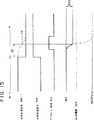
FIG. 15 shows horizontal scanning signals h (m−1) and h (m), the precharge signal PC in the mth horizontal scanning period, and the potential of the xth data signal line Sx shown in FIG. . The horizontal scanning signals h (m−1) and h (m) are respectively applied to the gates of all the switching
Here, when this horizontal scanning signal h (m−1) is applied to the gate of the
As shown in FIG. 15, when the waveform is rounded, the (m-1) th scanning signal is ended even though the (m-1) th original horizontal scanning period is ended and the mth horizontal scanning period is started. A voltage exceeding the threshold voltage Vth of the
Here, as shown in FIG. 15, it is assumed that in the (m−1) th horizontal scanning period, a data signal potential of 8V is charged in the data signal line Sx and halftone display is performed.
At this time, when the precharge signal is turned on within the period t2, the data signal line Sx is precharged to the first precharge potential PV1 (4V) as shown by the broken line in FIG. That is, the data signal line Sx is discharged from 8V to 4V, and in FIG. 15, the switching
For this reason, the charge of the
The rounding of the waveform of the horizontal scanning signal, which is the cause of this phenomenon, is caused by the load time constant described below.
This load is a parasitic resistance and a parasitic capacitance of the
In other words, since precharge is performed simultaneously for all the data signal lines 112, the pixel that is farther from the
(Improved precharge operation)
A timing chart showing the liquid crystal device of the present embodiment is shown in FIG. 1, a timing chart solving the first problem shown in FIG. 13 is shown in FIG. 5, and a timing chart solving the second problem shown in FIG. Is shown in FIG.
In the liquid crystal device of the first embodiment, the pixels are based on the data signals sampled in the subsequent sampling periods h1, h2, h3,... Within the precharge period T2 set in the blanking period TB shown in FIG. Each data signal line is precharged with the same polarity as the voltage applied to the.
In the present embodiment, as shown in FIG. 1, after the (m-1) th horizontal scanning signal h (m-1) is turned on and the (m-1) th horizontal scanning period is started, the pre-processing is performed after the elapse of the period T3. The charge signal PC becomes high, and the precharge period T2 is started. Further, after the precharge period T2 ends in the blanking period TB, the sampling signal S1 for the first pixel becomes high after the elapse of the period T1, and thereafter, the other sampling signals S2, S3,.
Here, in order to solve the first problem shown in FIG. 13 and improve the display quality at the first pixel (m, 1), the period T1 shown in FIGS. Is set to T1 ≧ τp or T4> τp.
In
When T1 ≧ τp, as shown in FIG. 5, the horizontal scanning signal h (m−1) is low, that is, all the switching
In the present embodiment, the X-side shift data signal DX becomes active before the precharge signal S1 for the first pixel becomes active. Therefore, if T1 ≧ τp, the result always satisfies T4> τp. . However, in order to solve the first problem described above, only T4> τp may be satisfied.
Next, in order to solve the second problem shown in FIG. 15 and improve the display quality at the pixel A (m−1, x), the period T3 shown in FIGS. The relationship with the time constant τh shown in
In
In this manner, as shown in FIG. 6, after all the switching
(How to set each period T1-T3)
As described above, each of the periods T1 and T3 is set to a period larger than the time constants τp and τh possessed by the load that affects the signal transmission time. The period T2 is set to a length that allows the data signal
These periods can be set by the adjustment circuit in the
In this manner, the periods T1 to T3 can be set to a certain length regardless of the driving frequency of the liquid crystal device. That is, by setting the periods T1 to T3 with reference to the X-side shift data signal DX, the periods T1 to T3 remain unchanged even if the drive frequency changes.
For example, for each liquid crystal device having an image data signal (video source) having each driving frequency as shown in FIG. 8, the fixed periods T1 to T3 are always set based on the X-side shift data signal DX. It can be easily handled. Here, in each figure of the combination of each liquid crystal device and video source (image data signal) in FIG. 8, the numbers indicate the number of pixels and the effective display period. In addition, when applying each video source to each device, any video source can be easily applied to each liquid crystal driving method by compressing and expanding the data signal as required. For example, when an SVGA video source is applied to a VGA liquid crystal device, it is converted to a video source suitable for the VGA liquid crystal device by performing digital signal processing and compressing the image data. Can do. This data signal compression / decompression can be performed by a digital signal processing IC. This can be done either by providing the circuit function in the data
Here, in the first embodiment, the first precharge potential PV1 is 8V and the second precharge potential PV2 is 4V. However, the present invention is not limited to this, and can be set as appropriate. It is.
Further, in the present embodiment, as an example, the case where white display and halftone display are respectively performed with the pixels A (m, 1) and A (m−1, n + x) has been described. Even when performing the above, all the above-mentioned problems can be solved.
In this embodiment, the black level potential on the positive polarity side is 11 V, the white level potential is 7 V, the black level potential on the negative polarity side is 1 V, and the white level potential is 5 V. However, the present invention is not limited to this. Never happen.
In the present embodiment, the description has been given on the assumption that the sampling switch is an N-type transistor that is turned on when a high-level sampling period signal is input. However, the sampling switch is not limited thereto. Can be constituted by a P-type transistor, and a low-level sampling period signal can be inputted. In this case, the X driver can easily realize a sampling period signal having a signal waveform opposite to that of the sample hold switch. Similarly, the switching element can be formed of a P-type transistor.
<
Electronic devices configured using the image display devices of the above-described embodiments include a display
The display
The
As an electronic device having such a configuration, a liquid crystal projector shown in FIG. 18, a personal computer (PC) and engineering workstation (EWS) compatible with multimedia shown in FIG. 19, a pager, or a mobile phone, a word processor, a television, a view Examples include a finder type or monitor direct-view type video tape recorder, electronic notebook, electronic desk calculator, car navigation device, POS terminal, and device equipped with a touch panel.
The liquid crystal projector shown in FIG. 18 is a projection type projector using a transmissive liquid crystal panel as a light valve, and uses, for example, a three-plate prism type optical system. In FIG. 18, in the
In the
A
In addition, this invention is not limited to the said embodiment, A various deformation | transformation implementation is possible within the range of the summary of this invention. For example, the present invention is not limited to being applied to driving the above-described various liquid crystal panels, but can also be applied to an image display device using electroluminescence, a plasma display device, a CRT, or the like.
In the above embodiment, an example in which a TFT is used as a switching element has been described. However, the switching element may be a two-terminal element such as an MIM. In this case, since the pixel is configured by connecting the two-terminal element and the pixel in series between the scanning signal line and the data signal line, the voltage difference between the two signal lines is supplied to the pixel.
In the above embodiment, the TFT is used as a switching element, and the substrate on which the liquid crystal panel element is formed is a glass or quartz substrate, but a semiconductor substrate may be used instead. In this case, not a TFT but a MOS transistor serves as a switching element.
Claims (10)
前記複数の走査信号線の少なくとも1本に接続された複数のスイッチング素子を水平走査期間にオンさせる水平走査信号を、前記複数の走査信号線に順次供給する走査側駆動手段と、
前記複数のデータ信号線の各々にそれぞれ接続され、サンプリング期間にデータ信号を順次サンプリングし前記複数のデータ信号線の各々に供給する複数のサンプリング用スイッチング手段と、
前記複数のサンプリング用スイッチング手段に前記サンプリング期間を設定するサンプリング信号を供給するデータ側駆動手段と、
前記複数のデータ信号線の各々に前記データ信号を順次供給する前記サンプリング期間に先立つプリチャージ期間に、当該データ信号に基づいて前記画素の液晶層に印加される電圧の極性と同一極性のプリチャージ電圧にて、前記複数のデータ信号線の各々を同時にプリチャージする複数のプリチャージ用スイッチング手段と、
同一水平走査期間内における前記プリチャージ期間終了から先頭の前記サンプリング用スイッチング手段の前記サンプリング期間が開始される迄の時間間隔を調整設定 する調整回路と、
を有し、
前記調整回路は、
基準クロック信号をカウントし、水平同期信号にてリセ ットされるカウンタと、
前記カウンタの出力をデコードするデコーダと、
前記デコーダの出力に基づき、前記プリチャージ信号及 び前記シフトデータ信号を出力する信号生成回路と、
を有し、
前記データ側駆動手段は、該データ側駆動手段を起動さ せるシフトデータ信号がアクティブとなった後に、前記 サンプリング信号を出力するものであり、
前記カウンタは、(m−1)番目の水平走査期間の終了 時からm番目の水平走査期間内の前記シフトデータ信号 がアクティブになるまでの期間(T1+T2+T3)と、前記 (m−1)番目の水平走査期間の終了時から前記m番目 の水平走査期間内に設定された前記プリチャージ期間 (T2)の終了までの期間(T3+T2)と、前記(m−1) 番目の水平走査期間の終了時から前記m番目の水平走査 期間内に設定された前記プリチャージ期間(T2)の開始 までの前記時間間隔(T3)と、にそれぞれ対応するカウ ント値を出力し、
前記デコーダは、前記カウンタからの前記カウント値に 基づいて、前記プリチャージ期間終了時から前記シフト データ信号がアクティブとなる迄の期間(T1)を設定す る信号を出力し、
前記時間間隔を、前記データ信号線に接続された前記プリチャージ用スイッチング手段での信号伝搬遅延時間よりも長く設定したことを特徴とする液晶装置。A switching element electrically connected to the liquid crystal layer is disposed in each of the plurality of pixels formed by the intersection of the plurality of data signal lines and the plurality of scanning signal lines, and the voltage applied to the liquid crystal layer is In a liquid crystal device that is driven by inverting the polarity every predetermined period,
Scanning-side drive means for sequentially supplying a plurality of switching elements connected to at least one of the plurality of scanning signal lines to the plurality of scanning signal lines in a horizontal scanning period;
A plurality of sampling switching means connected to each of the plurality of data signal lines, sequentially sampling a data signal during a sampling period, and supplying the data signal to each of the plurality of data signal lines;
Data-side driving means for supplying a sampling signal for setting the sampling period to the plurality of sampling switching means;
A precharge having the same polarity as the voltage applied to the liquid crystal layer of the pixel based on the data signal in a precharge period preceding the sampling period for sequentially supplying the data signal to each of the plurality of data signal lines A plurality of precharge switching means for simultaneously precharging each of the plurality of data signal lines with a voltage ;
An adjustment circuit that adjusts and sets a time interval from the end of the precharge period within the same horizontal scanning period to the start of the sampling period of the sampling switching means at the head ;
Have
The adjustment circuit includes:
Counting the reference clock signal, a counter which is reset at a horizontal synchronizing signal,
A decoder for decoding the output of the counter;
Based on the output of the decoder, a signal generating circuit for outputting the pre-charge signal及 beauty the shift data signal,
Have
The data side driving means outputs the sampling signal after a shift data signal that activates the data side driving means becomes active ,
The counter includes a period (T1 + T2 + T3) from the end of the (m−1) th horizontal scanning period until the shift data signal in the mth horizontal scanning period becomes active, and the (m−1) th horizontal scanning period . A period (T3 + T2) from the end of the horizontal scanning period to the end of the precharge period (T2) set in the mth horizontal scanning period, and the end of the (m−1) th horizontal scanning period outputs count value the time interval (T3), respectively to the to the beginning of the m-th of the precharge period set in the horizontal scanning period (T2) from,
Said decoder, based on the count value from the counter, the shift data signal from the time the precharge period ends outputs the signal to set the time period (T1) up to the active,
The liquid crystal device according to claim 1, wherein the time interval is set longer than a signal propagation delay time in the precharge switching means connected to the data signal line.
前記時間間隔は、前記プリチャージ用スイッチング手段及び前記プリチャージ電位供給手段がそれぞれ有する負荷に基づく各時定数の和よりも大きく設定されたものであることを特徴とする液晶装置。In claim 1,
The liquid crystal device according to claim 1, wherein the time interval is set to be larger than a sum of time constants based on loads of the precharge switching unit and the precharge potential supply unit.
前記複数の走査信号線の少なくとも1本に接続された複数のスイッチング素子を水平走査期間にオンさせる水平走査信号を、前記複数の走査信号線に順次供給する少なくとも一つの走査側駆動手段と、
前記複数のデータ信号線の各々にそれぞれ接続され、サンプリング期間にデータ信号を順次サンプリングし前記複数のデータ信号線の各々に供給する複数のサンプリング用スイッチング手段と、
シフトクロックに基づいてシフトデータ信号を転送するシフトレジスタを含み、前記複数のサンプリング用スイッチング手段についてそれぞれ前記サンプリング期間を設定するサンプリング信号を供給するデータ側駆動手段と、
前記複数のデータ信号線の各々に対して前記データ信号を順次供給する前記サンプリング期間に先立つプリチャージ期間にプリチャージ信号が供給されるとともに、当該データ信号に基づいて前記画素の液晶層に印加される電圧の極性と同一極性のプリチャージ電圧にて、前記複数のデータ信号線の各々を同時にプリチャージする複数のプリチャージ用スイッチング手段と、
(m−1)番目の水平走査期間の終了時から、m番目の水平走査期間内に設定されたプリチャージ期間の開始時迄の時間間隔を調整設定する調整回路と、を有し、
前記調整回路は、
基準クロック信号をカウントし、水平同期信号にてリセットされるカウンタと、
前記カウンタの出力をデコードして、前記時間間隔を設定する信号を出力するデコーダと、
前記デコーダの出力に基づき、前記プリチャージ信号及び前記シフトデータ信号を出力する信号生成回路と、
を有し、
前記カウンタは、(m−1)番目の水平走査期間の終了 時からm番目の水平走査期間内の前記シフトデータ信号 がアクティブになるまでの期間(T1+T2+T3)と、前記 (m−1)番目の水平走査期間の終了時から前記m番目 の水平走査期間内に設定された前記プリチャージ期間 (T2)の終了までの期間(T3+T2)と、前記(m−1) 番目の水平走査期間の終了時から前記m番目の水平走査 期間内に設定された前記プリチャージ期間(T2)の開始 までの前記時間間隔(T3)と、にそれぞれ対応するカウ ント値を出力し、
前記デコーダ出力に基づいて、前記時間間隔(T3)が、前記少なくとも一つの走査側駆動手段から最も遠い位置の画素に至る水平走査信号の信号伝搬遅延時間よりも長く設定されることを特徴とする液晶装置。A switching element electrically connected to the liquid crystal layer is disposed in each of the plurality of pixels formed by the intersection of the plurality of data signal lines and the plurality of scanning signal lines, and the voltage applied to the liquid crystal layer is In a liquid crystal device that is driven by inverting the polarity every predetermined period,
At least one scanning-side driving unit that sequentially supplies a plurality of switching elements connected to at least one of the plurality of scanning signal lines to the plurality of scanning signal lines in a horizontal scanning period;
A plurality of sampling switching means connected to each of the plurality of data signal lines, sequentially sampling a data signal during a sampling period, and supplying the data signal to each of the plurality of data signal lines;
A data-side drive unit that includes a shift register that transfers a shift data signal based on a shift clock, and that supplies a sampling signal that sets the sampling period for each of the plurality of sampling switching units;
A precharge signal is supplied in a precharge period preceding the sampling period for sequentially supplying the data signals to each of the plurality of data signal lines, and applied to the liquid crystal layer of the pixel based on the data signals. A plurality of precharge switching means for simultaneously precharging each of the plurality of data signal lines with a precharge voltage having the same polarity as the voltage of
An adjustment circuit for adjusting and setting a time interval from the end of the (m−1) th horizontal scanning period to the start of the precharge period set in the mth horizontal scanning period;
The adjustment circuit includes:
A counter that counts the reference clock signal and is reset by the horizontal synchronization signal;
A decoder that decodes the output of the counter and outputs a signal for setting the time interval;
A signal generation circuit for outputting the precharge signal and the shift data signal based on the output of the decoder;
Have
The counter includes a period (T1 + T2 + T3) from the end of the (m−1) th horizontal scanning period until the shift data signal in the mth horizontal scanning period becomes active, and the (m−1) th horizontal scanning period . A period (T3 + T2) from the end of the horizontal scanning period to the end of the precharge period (T2) set in the mth horizontal scanning period, and the end of the (m−1) th horizontal scanning period outputs count value the time interval (T3), respectively to the to the beginning of the m-th of the precharge period set in the horizontal scanning period (T2) from,
Based on the decoder output, the time interval (T3) is set longer than a signal propagation delay time of a horizontal scanning signal reaching a pixel farthest from the at least one scanning side driving unit. Liquid crystal device.
前記時間間隔は、1本の前記走査信号線及び前記最も遠い画素のスイッチング素子がそれぞれ有する負荷に基づく各時定数の和よりも大きく設定されたものであることを特徴とする液晶装置。In claim 3 ,
The liquid crystal device according to claim 1, wherein the time interval is set to be larger than a sum of time constants based on a load of each of the scanning signal line and the switching element of the farthest pixel.
前記液晶層が封入された一対の基板を有し、
前記複数のサンプリング用スイッチング手段は、前記一対の基板の一方に形成された複数のスイッチング素子にて形成されることを特徴とする液晶装置。In any one of Claims 1 thru | or 4 ,
A pair of substrates enclosing the liquid crystal layer;
The liquid crystal device, wherein the plurality of sampling switching means are formed by a plurality of switching elements formed on one of the pair of substrates.
前記スイッチング素子は、MOSトランジスタまたは薄膜トランジスタであることを特徴とする液晶装置。In claim 5 ,
The liquid crystal device, wherein the switching element is a MOS transistor or a thin film transistor.
前記複数の走査信号線の少なくとも1本に接続された複数のスイッチング素子を水平走査期間にオンさせる水平走査信号を、前記複数の走査信号線に順次供給し、
シフトクロックに基づいてシフトデータ信号を転送する シフトレジスタを含むデータ側駆動手段により、前記複数のデータ信号線にそれぞれ接続された複数のサンプリング用スイッチング手段にサンプリング信号を供給し、 前記複数のサンプリング用スイッチング手段によりデータ信号を各々のサンプリング期間にサンプリングして、前記複数のデータ信号線の各々に供給し、
前記複数のデータ信号線に接続された複数のプリチャージ用スイッチング手段を介して、前記複数のデータ信号線の各々に前記データ信号を供給する前記各々のサンプリング期間に先立つプリチャージ期間に、該サンプリング期間にてサンプリングされるデータ信号に基づいて前記画素に印加される電圧の極性と同一極性のプリチャージ電圧にて、前記複数のデータ信号線の各々を同時にプリチャージし、
前記プリチャージ期間終了から、前記水平走査期間での先頭のサンプリング期間が開始される迄の時間間隔を一定とし、前記時間間隔を、前記1本のデータ信号線に接続された前記プリチャージ用スイッチング手段での信号伝搬遅延時間よりも長く設定し、
前記時間間隔を設定する工程は、
基準クロック信号をカウントし、水平同期信号にてリセ ットされるカウンタにて、(m−1)番目の水平走査期 間の終了時からm番目の水平走査期間内の前記シフトデ ータ信号がアクティブになるまでの期間(T1+T2+T3) と、前記(m−1)番目の水平走査期間の終了時から前 記m番目の水平走査期間内に設定された前記プリチャー ジ期間(T2)の終了までの期間(T3+T2)と、前記(m −1)番目の水平走査期間の終了時から前記m番目の水 平走査期間内に設定された前記プリチャージ期間(T2) の開始までの前記時間間隔(T3)と、にそれぞれ対応す るカウント値を出力する工程と、
と、
前記カウンタの出力をデコーダにてデコードして、前記 プリチャージ期間終了時から前記シフトデータ信号がア クティブとなる迄の期間(T1)を設定する信号を出力す る工程と、
を含むことを特徴とする液晶装置の駆動方法。A liquid crystal device in which a switching element electrically connected to the liquid crystal layer is disposed in each of the plurality of pixels formed by the intersection of the plurality of data signal lines and the plurality of scanning signal lines is applied to the liquid crystal layer. In a driving method of a liquid crystal device for driving by inverting the polarity of a voltage every predetermined period,
A horizontal scanning signal for sequentially turning on a plurality of switching elements connected to at least one of the plurality of scanning signal lines in a horizontal scanning period is sequentially supplied to the plurality of scanning signal lines,
The data side driving means including a shift register for transferring a shift data signal based on a shift clock supplies a sampling signal to a plurality of sampling switching means respectively connected to the plurality of data signal lines, and The data signal is sampled in each sampling period by the switching means and supplied to each of the plurality of data signal lines,
In the precharge period preceding each sampling period for supplying the data signal to each of the plurality of data signal lines via a plurality of precharge switching means connected to the plurality of data signal lines, the sampling is performed. Precharging each of the plurality of data signal lines simultaneously with a precharge voltage having the same polarity as the voltage applied to the pixel based on a data signal sampled in a period;
The time interval from the end of the precharge period to the start of the first sampling period in the horizontal scanning period is constant, and the time interval is set to the precharge switching connected to the one data signal line. Set longer than the signal propagation delay time in the means ,
The step of setting the time interval includes
Counting the reference clock signal at a counter which is reset at a horizontal synchronizing signal, said Shifutode data signal in the m-th horizontal scanning period from the end between the (m-1) th horizontal scanning period and the period (T1 + T2 + T3) to become active, the (m-1) -th said precharge period is set before Symbol m-th horizontal scanning period from the end of the horizontal scanning period until the end of (T2) a period (T3 + T2), the (m -1) -th time interval from the end of the horizontal scanning period to the start of said m-th of the precharge period is set to horizontal scanning period (T2) (T3 ), a step of outputting a count value that corresponds respectively to,
When,
By decoding the output of the counter by the decoder, the steps the shift data signal from the time the precharge period end you output a signal for setting the time period (T1) up to the active,
A method for driving a liquid crystal device, comprising:
前記複数の走査信号線の少なくとも1本に接続された複数のスイッチング素子を水平走査期間にオンさせる水平走査信号を、少なくとも一つの走査側駆動手段から前記複数の走査信号線に順次供給し、
シフトクロックに基づいてシフトデータ信号を転送するシフトレジスタを含むデータ側駆動手段により、前記複数のデータ信号線にそれぞれ接続された複数のサンプリング用スイッチング手段にサンプリング信号を供給して、前記複数のサンプリング用スイッチング手段により、データ信号を各々のサンプリング期間にサンプリングして、前記複数のデータ信号線の各々に供給し、
前記複数のデータ信号線に接続された複数のプリチャージ用スイッチング手段に共通するプリチャージ信号を供給し、前記複数のプリチャージ用スイッチング手段を介して、前記複数のデータ信号線の各々に前記データ信号を供給する前記各々のサンプリング期間に先立つプリチャージ期間に、該サンプリング期間にてサンプリングされるデータ信号に基づいて前記画素に印加される電圧の極性と同一極性のプリチャージ電圧にて、前記複数のデータ信号線の各々を同時にプリチャージし、
基準クロック信号をカウントし水平同期信号にてリセットされるカウンタの出力をデコードするデコーダ出力に基づいて、前記プリチャージ信号及び前記シフトデータ信号を出力し、(m−1)番目の水平走査期間の終了時から、m番目の水平走査期間内に設定されたプリチャージ期間の開始時迄の時間間隔を設定し、
前記時間間隔を設定する工程は、
前記カウンタが、(m−1)番目の水平走査期間の終了 時からm番目の水平走査期間内の前記シフトデータ信号 がアクティブになるまでの期間(T1+T2+T3)と、前記 (m−1)番目の水平走査期間の終了時から前記m番目 の水平走査期間内に設定された前記プリチャージ期間 (T2)の終了までの期間(T3+T2)と、前記(m−1) 番目の水平走査期間の終了時から前記m番目の水平走査 期間内に設定された前記プリチャージ期間(T2)の開始 までの前記時間間隔(T3)と、にそれぞれ対応するカウ ント値を出力する工程を含み、前記時間間隔(T3)が、前記少なくとも一つの走査側駆動手段から最も遠い位置の画素に至る水平走査信号の信号伝搬遅延時間よりも長く設定されたものであることを特徴とする液晶装置の駆動方法。A liquid crystal device in which a switching element electrically connected to the liquid crystal layer is disposed in each of the plurality of pixels formed by the intersection of the plurality of data signal lines and the plurality of scanning signal lines is applied to the liquid crystal layer. In a driving method of a liquid crystal device for driving by inverting the polarity of a voltage every predetermined period,
A horizontal scanning signal for turning on a plurality of switching elements connected to at least one of the plurality of scanning signal lines in a horizontal scanning period is sequentially supplied from at least one scanning side driving unit to the plurality of scanning signal lines,
A plurality of sampling units are provided by supplying a sampling signal to a plurality of sampling switching units respectively connected to the plurality of data signal lines by a data side driving unit including a shift register for transferring a shift data signal based on a shift clock. Switching means for sampling a data signal in each sampling period and supplying each of the plurality of data signal lines;
A precharge signal common to a plurality of precharge switching means connected to the plurality of data signal lines is supplied, and the data is supplied to each of the plurality of data signal lines via the plurality of precharge switching means. In the precharge period prior to each of the sampling periods for supplying a signal, the plurality of the precharge voltages having the same polarity as the voltage applied to the pixel based on the data signal sampled in the sampling period. Simultaneously precharge each of the data signal lines,
The precharge signal and the shift data signal are output based on the decoder output that counts the reference clock signal and decodes the output of the counter that is reset by the horizontal synchronization signal, and outputs the ( m−1) th horizontal scanning period. Set the time interval from the end to the start of the precharge period set in the mth horizontal scanning period ,
The step of setting the time interval includes
The counter has a period (T1 + T2 + T3) from the end of the (m−1) th horizontal scanning period until the shift data signal in the mth horizontal scanning period becomes active, and the (m−1) th horizontal scanning period . A period (T3 + T2) from the end of the horizontal scanning period to the end of the precharge period (T2) set in the mth horizontal scanning period, and the end of the (m−1) th horizontal scanning period comprising the step of outputting the count value wherein the time interval between (T3), respectively to the to the beginning of the m-th of the precharge period set in the horizontal scanning period (T2) from the time interval ( A method for driving a liquid crystal device, wherein T3) is set longer than a signal propagation delay time of a horizontal scanning signal reaching a pixel farthest from the at least one scanning side driving means.
Applications Claiming Priority (2)
| Application Number | Priority Date | Filing Date | Title |
|---|---|---|---|
| JP20707497 | 1997-07-16 | ||
| PCT/JP1997/003601 WO1999004385A1 (en) | 1997-07-16 | 1997-10-08 | Liquid crystal device, method for driving the same, and projection display and electronic equipment made using the same |
Publications (1)
| Publication Number | Publication Date |
|---|---|
| JP3661193B2 true JP3661193B2 (en) | 2005-06-15 |
Family
ID=16533779
Family Applications (1)
| Application Number | Title | Priority Date | Filing Date |
|---|---|---|---|
| JP51817498A Expired - Fee Related JP3661193B2 (en) | 1997-07-16 | 1997-10-08 | Liquid crystal device and driving method thereof, and projection display device and electronic apparatus using the same |
Country Status (3)
| Country | Link |
|---|---|
| US (2) | US6307532B1 (en) |
| JP (1) | JP3661193B2 (en) |
| WO (1) | WO1999004385A1 (en) |
Families Citing this family (31)
| Publication number | Priority date | Publication date | Assignee | Title |
|---|---|---|---|---|
| US6677613B1 (en) * | 1999-03-03 | 2004-01-13 | Semiconductor Energy Laboratory Co., Ltd. | Semiconductor device and method of fabricating the same |
| TW564388B (en) * | 1999-05-11 | 2003-12-01 | Toshiba Corp | Method of driving flat-panel display device |
| US6876145B1 (en) | 1999-09-30 | 2005-04-05 | Semiconductor Energy Laboratory Co., Ltd. | Organic electroluminescent display device |
| JP2001188217A (en) * | 1999-10-20 | 2001-07-10 | Sharp Corp | Active matrix liquid crystal display device, and driving method and manufacturing method therefor |
| JP3777913B2 (en) * | 1999-10-28 | 2006-05-24 | 株式会社日立製作所 | Liquid crystal driving circuit and liquid crystal display device |
| JP3428550B2 (en) * | 2000-02-04 | 2003-07-22 | 日本電気株式会社 | Liquid crystal display |
| US6806015B2 (en) * | 2001-02-06 | 2004-10-19 | Konica Corporation | Image forming method using flattened spheroidal toner |
| TW562972B (en) * | 2001-02-07 | 2003-11-21 | Toshiba Corp | Driving method for flat-panel display device |
| KR100441523B1 (en) * | 2001-09-28 | 2004-07-23 | 삼성에스디아이 주식회사 | Method and apparatus to control drive-power for plasma display panel |
| JP4188603B2 (en) * | 2002-01-16 | 2008-11-26 | 株式会社日立製作所 | Liquid crystal display device and driving method thereof |
| KR100438784B1 (en) | 2002-01-30 | 2004-07-05 | 삼성전자주식회사 | Source driver output circuit of thin film transistor liquid crystal displayer |
| JP2004094014A (en) * | 2002-09-02 | 2004-03-25 | Hitachi Displays Ltd | Display device |
| GB0316482D0 (en) * | 2003-07-15 | 2003-08-20 | Koninkl Philips Electronics Nv | Active matrix array device |
| KR100989344B1 (en) * | 2003-09-02 | 2010-10-25 | 삼성전자주식회사 | Method and apparatus for driving a gray data, and display device having the same |
| JP4385730B2 (en) * | 2003-11-13 | 2009-12-16 | セイコーエプソン株式会社 | Electro-optical device driving method, electro-optical device, and electronic apparatus |
| JP4289269B2 (en) * | 2004-03-01 | 2009-07-01 | セイコーエプソン株式会社 | Optical display device, optical display device control program, and optical display device control method |
| JP4170242B2 (en) * | 2004-03-04 | 2008-10-22 | シャープ株式会社 | Liquid crystal display device and driving method of liquid crystal display device |
| JP5105699B2 (en) * | 2004-06-18 | 2012-12-26 | 三菱電機株式会社 | Display device |
| US7161970B2 (en) * | 2004-09-10 | 2007-01-09 | Ftd Solutions Pte, Ltd. | Spread spectrum clock generator |
| DE102007010601A1 (en) | 2007-03-05 | 2008-09-25 | Siemens Audiologische Technik Gmbh | Hearing system with distributed signal processing and corresponding method |
| TWI353576B (en) * | 2007-03-21 | 2011-12-01 | Novatek Microelectronics Corp | Lcd device driven by pre-charge procedure |
| TW201040925A (en) * | 2009-05-13 | 2010-11-16 | Chunghwa Picture Tubes Ltd | Method for driving a tri-gate TFT LCD |
| KR101740943B1 (en) * | 2009-09-24 | 2017-06-15 | 가부시키가이샤 한도오따이 에네루기 켄큐쇼 | Display device |
| US20140078196A1 (en) * | 2011-05-31 | 2014-03-20 | Sharp Kabushiki Kaisha | Drive circuit and drive method for display device |
| JP2013044891A (en) * | 2011-08-23 | 2013-03-04 | Sony Corp | Display device and electronic apparatus |
| CN103165059B (en) * | 2011-12-09 | 2016-01-20 | 群康科技(深圳)有限公司 | Display drive method, driver module and display device |
| TWI455092B (en) * | 2011-12-09 | 2014-10-01 | Innolux Corp | Display driving method, driving module and display apparatus |
| JP2015184313A (en) * | 2014-03-20 | 2015-10-22 | シナプティクス・ディスプレイ・デバイス合同会社 | display drive circuit |
| JPWO2016208321A1 (en) * | 2015-06-26 | 2018-04-12 | ソニー株式会社 | Control circuit, display device, electronic device and projection display device |
| US10490154B2 (en) | 2016-12-01 | 2019-11-26 | Seiko Epson Corporation | Electro-optical device and electronic device |
| CN113570997A (en) * | 2021-07-30 | 2021-10-29 | 北京京东方显示技术有限公司 | Display device |
Family Cites Families (5)
| Publication number | Priority date | Publication date | Assignee | Title |
|---|---|---|---|---|
| JP2579467B2 (en) | 1986-08-07 | 1997-02-05 | セイコーエプソン株式会社 | Liquid crystal display device and driving method thereof |
| US4963860A (en) * | 1988-02-01 | 1990-10-16 | General Electric Company | Integrated matrix display circuitry |
| JP2830004B2 (en) | 1989-02-02 | 1998-12-02 | ソニー株式会社 | Liquid crystal display device |
| JPH04321093A (en) | 1991-04-22 | 1992-11-11 | Nec Corp | Projection type display device |
| US5510807A (en) | 1993-01-05 | 1996-04-23 | Yuen Foong Yu H.K. Co., Ltd. | Data driver circuit and associated method for use with scanned LCD video display |
-
1997
- 1997-10-08 WO PCT/JP1997/003601 patent/WO1999004385A1/en active Application Filing
- 1997-10-08 JP JP51817498A patent/JP3661193B2/en not_active Expired - Fee Related
- 1997-10-08 US US09/254,688 patent/US6307532B1/en not_active Expired - Lifetime
-
2001
- 2001-08-09 US US09/924,510 patent/US6545657B2/en not_active Expired - Lifetime
Also Published As
| Publication number | Publication date |
|---|---|
| WO1999004385A1 (en) | 1999-01-28 |
| US20020024486A1 (en) | 2002-02-28 |
| US6545657B2 (en) | 2003-04-08 |
| US6307532B1 (en) | 2001-10-23 |
Similar Documents
| Publication | Publication Date | Title |
|---|---|---|
| JP3661193B2 (en) | Liquid crystal device and driving method thereof, and projection display device and electronic apparatus using the same | |
| JP3704716B2 (en) | Liquid crystal device and driving method thereof, and projection display device and electronic apparatus using the same | |
| JP3832125B2 (en) | Electro-optical device and electronic apparatus | |
| US7932885B2 (en) | Electro-optical device and electronic apparatus with dummy data lines operated substantially simultaneously | |
| US7602361B2 (en) | Electro-optical device, driving circuit, method, and apparatus to clear residual images between frames and precharge voltage for subsequent operation | |
| US7002537B1 (en) | Method of driving electrooptic device, driving circuit, electrooptic device, and electronic apparatus | |
| US7495650B2 (en) | Electro-optical device and electronic apparatus | |
| US8063875B2 (en) | Electrooptic device, scanning-line driving circuit, method for driving the same, and electronic device | |
| US20050206597A1 (en) | Electro-optical device, method for driving electro-optical device, driving circuit, and electronic apparatus | |
| US20120120044A1 (en) | Liquid crystal display device and method for driving the same | |
| JP3687344B2 (en) | Liquid crystal device and driving method thereof, and projection display device and electronic apparatus using the same | |
| KR20070119346A (en) | Gate driving circuit and driving method thereof for lcd | |
| US6417847B1 (en) | Flat-panel display device, array substrate, and method for driving flat-panel display device | |
| JP3613942B2 (en) | Image display device, image display method, electronic apparatus using the same, and projection display device | |
| JP3661324B2 (en) | Image display device, image display method, display drive device, and electronic apparatus using the same | |
| US9087493B2 (en) | Liquid crystal display device and driving method thereof | |
| KR20070104832A (en) | Liquid crystal device, control circuit therefor, and electronic apparatus | |
| JP2001159883A (en) | Driving method for optoelectronic device, drive circuit therefor, and optoelectronic device as well as electronic apparatus | |
| US7684092B2 (en) | Electro-optical device and writing circuit of electro-optical device | |
| JP3525763B2 (en) | Electro-optical device driving circuit, electro-optical device driving method, electro-optical device, and electronic apparatus | |
| JP4258501B2 (en) | Electro-optical device, electronic apparatus, and driving method of electro-optical device | |
| JP2003202847A (en) | Liquid crystal device and driving method therefor, and projection type display device and electronic equipment using the same | |
| JP4353203B2 (en) | Electro-optical device, electronic apparatus, and driving method of electro-optical device | |
| JP3726589B2 (en) | Electro-optical device driving circuit, electro-optical device, and electro-optical device driving method | |
| JP2004309847A (en) | Driving method and driving circuit for electro-optic device, method of setting selection potential, electro-optic device and electronic equipment |
Legal Events
| Date | Code | Title | Description |
|---|---|---|---|
| A521 | Written amendment |
Free format text: JAPANESE INTERMEDIATE CODE: A523 Effective date: 20040318 |
|
| A871 | Explanation of circumstances concerning accelerated examination |
Free format text: JAPANESE INTERMEDIATE CODE: A871 Effective date: 20040318 |
|
| A975 | Report on accelerated examination |
Free format text: JAPANESE INTERMEDIATE CODE: A971005 Effective date: 20040517 |
|
| A131 | Notification of reasons for refusal |
Free format text: JAPANESE INTERMEDIATE CODE: A131 Effective date: 20040601 |
|
| A521 | Written amendment |
Free format text: JAPANESE INTERMEDIATE CODE: A523 Effective date: 20040728 |
|
| A02 | Decision of refusal |
Free format text: JAPANESE INTERMEDIATE CODE: A02 Effective date: 20041130 |
|
| A521 | Written amendment |
Free format text: JAPANESE INTERMEDIATE CODE: A523 Effective date: 20050126 |
|
| A911 | Transfer to examiner for re-examination before appeal (zenchi) |
Free format text: JAPANESE INTERMEDIATE CODE: A911 Effective date: 20050217 |
|
| TRDD | Decision of grant or rejection written | ||
| A01 | Written decision to grant a patent or to grant a registration (utility model) |
Free format text: JAPANESE INTERMEDIATE CODE: A01 Effective date: 20050301 |
|
| A61 | First payment of annual fees (during grant procedure) |
Free format text: JAPANESE INTERMEDIATE CODE: A61 Effective date: 20050314 |
|
| R150 | Certificate of patent or registration of utility model |
Free format text: JAPANESE INTERMEDIATE CODE: R150 |
|
| FPAY | Renewal fee payment (event date is renewal date of database) |
Free format text: PAYMENT UNTIL: 20080401 Year of fee payment: 3 |
|
| FPAY | Renewal fee payment (event date is renewal date of database) |
Free format text: PAYMENT UNTIL: 20090401 Year of fee payment: 4 |
|
| FPAY | Renewal fee payment (event date is renewal date of database) |
Free format text: PAYMENT UNTIL: 20090401 Year of fee payment: 4 |
|
| FPAY | Renewal fee payment (event date is renewal date of database) |
Free format text: PAYMENT UNTIL: 20100401 Year of fee payment: 5 |
|
| FPAY | Renewal fee payment (event date is renewal date of database) |
Free format text: PAYMENT UNTIL: 20110401 Year of fee payment: 6 |
|
| FPAY | Renewal fee payment (event date is renewal date of database) |
Free format text: PAYMENT UNTIL: 20110401 Year of fee payment: 6 |
|
| FPAY | Renewal fee payment (event date is renewal date of database) |
Free format text: PAYMENT UNTIL: 20120401 Year of fee payment: 7 |
|
| FPAY | Renewal fee payment (event date is renewal date of database) |
Free format text: PAYMENT UNTIL: 20130401 Year of fee payment: 8 |
|
| FPAY | Renewal fee payment (event date is renewal date of database) |
Free format text: PAYMENT UNTIL: 20130401 Year of fee payment: 8 |
|
| FPAY | Renewal fee payment (event date is renewal date of database) |
Free format text: PAYMENT UNTIL: 20140401 Year of fee payment: 9 |
|
| LAPS | Cancellation because of no payment of annual fees |