JP3659855B2 - Tilt sensor - Google Patents
Tilt sensor Download PDFInfo
- Publication number
- JP3659855B2 JP3659855B2 JP2000048559A JP2000048559A JP3659855B2 JP 3659855 B2 JP3659855 B2 JP 3659855B2 JP 2000048559 A JP2000048559 A JP 2000048559A JP 2000048559 A JP2000048559 A JP 2000048559A JP 3659855 B2 JP3659855 B2 JP 3659855B2
- Authority
- JP
- Japan
- Prior art keywords
- differential
- circuit board
- common electrode
- voltage
- printed circuit
- Prior art date
- Legal status (The legal status is an assumption and is not a legal conclusion. Google has not performed a legal analysis and makes no representation as to the accuracy of the status listed.)
- Expired - Fee Related
Links
- 239000003990 capacitor Substances 0.000 claims description 47
- 238000006243 chemical reaction Methods 0.000 claims description 38
- 239000007788 liquid Substances 0.000 claims description 38
- 238000012545 processing Methods 0.000 claims description 29
- 238000001514 detection method Methods 0.000 claims description 18
- 238000005259 measurement Methods 0.000 claims description 8
- 239000003921 oil Substances 0.000 description 8
- 230000005484 gravity Effects 0.000 description 7
- RYGMFSIKBFXOCR-UHFFFAOYSA-N Copper Chemical compound [Cu] RYGMFSIKBFXOCR-UHFFFAOYSA-N 0.000 description 6
- 229910052802 copper Inorganic materials 0.000 description 6
- 239000010949 copper Substances 0.000 description 6
- 230000002093 peripheral effect Effects 0.000 description 5
- 230000006641 stabilisation Effects 0.000 description 5
- 238000011105 stabilization Methods 0.000 description 5
- 229910000679 solder Inorganic materials 0.000 description 4
- 238000010586 diagram Methods 0.000 description 3
- XUIMIQQOPSSXEZ-UHFFFAOYSA-N Silicon Chemical compound [Si] XUIMIQQOPSSXEZ-UHFFFAOYSA-N 0.000 description 2
- 239000000853 adhesive Substances 0.000 description 2
- 230000001070 adhesive effect Effects 0.000 description 2
- 230000003321 amplification Effects 0.000 description 2
- 230000000903 blocking effect Effects 0.000 description 2
- 230000007423 decrease Effects 0.000 description 2
- 230000000694 effects Effects 0.000 description 2
- 239000003822 epoxy resin Substances 0.000 description 2
- 239000004744 fabric Substances 0.000 description 2
- 239000011521 glass Substances 0.000 description 2
- 238000003780 insertion Methods 0.000 description 2
- 230000037431 insertion Effects 0.000 description 2
- 238000003199 nucleic acid amplification method Methods 0.000 description 2
- 230000010355 oscillation Effects 0.000 description 2
- 239000004033 plastic Substances 0.000 description 2
- 229920000647 polyepoxide Polymers 0.000 description 2
- 229910052710 silicon Inorganic materials 0.000 description 2
- 239000010703 silicon Substances 0.000 description 2
- 239000004020 conductor Substances 0.000 description 1
- 230000003247 decreasing effect Effects 0.000 description 1
- 238000007654 immersion Methods 0.000 description 1
- 238000002347 injection Methods 0.000 description 1
- 239000007924 injection Substances 0.000 description 1
- 238000012544 monitoring process Methods 0.000 description 1
- 238000005476 soldering Methods 0.000 description 1
- 238000013022 venting Methods 0.000 description 1
Images


Classifications
-
- G—PHYSICS
- G01—MEASURING; TESTING
- G01C—MEASURING DISTANCES, LEVELS OR BEARINGS; SURVEYING; NAVIGATION; GYROSCOPIC INSTRUMENTS; PHOTOGRAMMETRY OR VIDEOGRAMMETRY
- G01C9/00—Measuring inclination, e.g. by clinometers, by levels
- G01C9/02—Details
- G01C9/06—Electric or photoelectric indication or reading means
-
- G—PHYSICS
- G01—MEASURING; TESTING
- G01C—MEASURING DISTANCES, LEVELS OR BEARINGS; SURVEYING; NAVIGATION; GYROSCOPIC INSTRUMENTS; PHOTOGRAMMETRY OR VIDEOGRAMMETRY
- G01C9/00—Measuring inclination, e.g. by clinometers, by levels
- G01C9/18—Measuring inclination, e.g. by clinometers, by levels by using liquids
- G01C9/20—Measuring inclination, e.g. by clinometers, by levels by using liquids the indication being based on the inclination of the surface of a liquid relative to its container
-
- G—PHYSICS
- G01—MEASURING; TESTING
- G01C—MEASURING DISTANCES, LEVELS OR BEARINGS; SURVEYING; NAVIGATION; GYROSCOPIC INSTRUMENTS; PHOTOGRAMMETRY OR VIDEOGRAMMETRY
- G01C9/00—Measuring inclination, e.g. by clinometers, by levels
- G01C9/02—Details
- G01C9/06—Electric or photoelectric indication or reading means
- G01C2009/062—Electric or photoelectric indication or reading means capacitive
-
- G—PHYSICS
- G01—MEASURING; TESTING
- G01C—MEASURING DISTANCES, LEVELS OR BEARINGS; SURVEYING; NAVIGATION; GYROSCOPIC INSTRUMENTS; PHOTOGRAMMETRY OR VIDEOGRAMMETRY
- G01C9/00—Measuring inclination, e.g. by clinometers, by levels
- G01C9/18—Measuring inclination, e.g. by clinometers, by levels by using liquids
- G01C2009/185—Measuring inclination, e.g. by clinometers, by levels by using liquids dielectric
Description
【0001】
【発明の属する技術分野】
この発明は、例えば重力方向に垂直な面に対する傾斜角度を検出し、検出された傾斜角度が所定値を超えたときに、警報を発したり、所定の制御を行わせるために用いて好適な静電容量式の傾斜センサに関する。
【0002】
【従来の技術】
この種の静電容量式の傾斜センサとして、例えば図5、図6に示すような構造の傾斜検出素子を使用するものが知られている(例えば実公平4−53528号公報、実公平5−14168号公報など参照)。
【0003】
図5は、この例の傾斜センサの傾斜検出素子の分解斜視図である。また、図6は、この傾斜検出素子を、その正面に垂直な面で切断した場合の断面図を示すものである。
【0004】
これらの図において、1はプリント基板で、例えばガラス布基材エポキシ樹脂積層板等の耐熱性部材からなる。このプリント基板1は、傾斜センサが傾斜検出対象物に取り付けられる時に、傾斜測定の基準面に対して垂直に配置される。図5では、この基準面は、二点鎖線で示す仮想線L0を含む面として示した。この基準面が、被測定面となる。この場合、傾斜角が0度とは、基準面が重力方向に垂直な線を含む状態である。
【0005】
このプリント基板1には、1対の差動電極2a,2bが、銅泊パターンによって、基準面およびプリント基板1面の両方に垂直な面と、プリント基板1との交差線(図5で二点鎖線で示す仮想線L1)により左右に分割される領域に、互いに電気的に独立に形成される。
【0006】
プリント基板1の差動電極2a,2bが形成される面とは反対側の面には、後述する傾斜センサの信号処理回路部が、プリント配線パターンと必要な電子部品とによって構成されて設けられる。差動電極2a,2bのそれぞれは、図5の電極点2c,2dからスルーホールを介してプリント基板1の信号処理回路部が形成される面の銅泊パターンに接続されるようにされている。
【0007】
そして、1対の差動電極2a,2bは、前記仮想線L1を対称軸として互いに線対称となる形状の電極パターンとして設けられる。また、この1対の差動電極2a,2bのそれぞれは、仮想線L1に垂直な仮想線L2を対称軸とした線対称な電極パターン形状ともされる。図5の例の場合には、差動電極2a,2bの形状は横向きの扇形に構成されている。
【0008】
図5の例の場合、差動電極2aおよび2bの円弧状周縁は、仮想線L1と仮想線L2との交点を中心とした円の一部の円弧とされている。この例の場合、その円の直径は、30mmとされている。
【0009】
3は共通電極板で、適当な剛性を持つ導電性部材で形成されている。この共通電極板3は、この板3と一体で、この板3から直角に曲げられた複数個の端子3a,3b,3c,3dが、プリント基板1に設けられている端子孔4a,4b,4c,4dに挿入され、プリント基板1の信号処理回路部が形成される面において半田付け固定されることにより、図6に示すように、差動電極2a,2bに対して一定の間隔を持って平行に保持される状態でプリント基板1に取り付けられる。
【0010】
5はオイルケースで、適当な柔軟性を有するプラスチックからなる。このケース5は、図6に示すように、断面がコ字状を有し、その端面がプリント基板1に、例えば両面テープ5Bなどの接着手段により接着されることにより、プリント基板1と共に密閉空間を形成する。
【0011】
この場合、差動電極2a,2bの周端縁と、共通電極板3の周端縁と、ケース5の端面の内周縁は同心円状に形成され、また、差動電極2a,2bと共通電極3とケース5の対向面はそれぞれ平行に形成されている。
【0012】
ケース5とプリント基板1とで形成される密閉空間内には、プリント基板1に設けられた貫通孔6からシリコン・オイル等の誘電性液体7が、密閉空間内の有効容積のほぼ1/2のレベル、すなわち図5の仮想線L2のレベルまで充填される。
【0013】
プリント基板1の貫通孔6は、誘電性液体7が封入された後、封止される。
【0014】
なお、8及び9は、外部の影響を遮断するための静電シールド板で、静電シールド板8は、ケース5およびその周辺を覆うようにプリント基板1に取り付けられ、静電シールド板9は、後述する信号処理回路部分を覆うようにプリント基板1に取り付けられる。
【0015】
図7は、この例の傾斜センサの信号処理回路部分の構成を示すものである。
【0016】
図7において、11は発振器であり、その発振信号の出力端子が、前述した図5および図6で説明した構成の傾斜検出素子10の共通電極板3に接続される。また、傾斜検出素子10の1対の差動電極2a,2bのそれぞれは、容量−電圧変換回路12a,12bの入力端子に接続される。
【0017】
これら容量−電圧変換回路12aおよび12bの出力端子は、それぞれ差動増幅回路13の一方および他方の入力端子に接続される。この差動増幅回路13からは傾斜センサの出力端子14が導出される。なお、信号処理回路部には電源安定化回路15が含まれており、この電源安定化回路15を通じた安定化電圧が発振器11や差動増幅回路13に、その電源電圧として供給される。
【0018】
信号処理回路部は、上述のように構成されているので、発振器11からの一定周波数の発振出力信号は、差動電極2aと共通電極板3とで構成される第1のコンデンサを通じて容量−電圧変換回路12aに供給されると共に、差動電極2bと共通電極板3とで構成される第2のコンデンサを通じて容量−電圧変換回路12bに供給される。このとき、容量−電圧変換回路12aおよび12bのそれぞれには、第1のコンデンサの容量値および第2のコンデンサの容量値のそれぞれに応じた波高値の信号が、それぞれ入力される。
【0019】
容量−電圧変換回路12aおよび12bは、それぞれの入力信号を整流し、平滑した電圧を出力する。したがって、容量−電圧変換回路12aおよび12bの出力電圧は、それぞれの入力信号の波高値、すなわち、第1のコンデンサの容量値および第2のコンデンサの容量値のそれぞれに応じた大きさとなる。
【0020】
したがって、差動増幅回路13からは、容量−電圧変換回路12aの出力電圧と、容量−電圧変換回路12bの出力電圧との差の電圧が得られ、それが傾斜センサの出力として、出力端子14に導出される。すなわち、差動増幅回路13からは、第1のコンデンサと第2のコンデンサの容量値の差に応じた出力電圧が得られる。
【0021】
以上のような構成の傾斜検出素子10および信号処理回路部を備える傾斜センサを、前述したように被測定物の傾斜測定の基準面となる面(以下、この面を被測定面という)上に設置する。このとき、傾斜検出素子10のプリント基板1面が、被測定面の被測定傾斜方向を含む面となるように設置する。
【0022】
なお、この明細書において、被測定面の被測定傾斜方向とは、測定しようとする傾斜の方向に被測定面が傾斜するときの被測定面の法線の移動方向であり、被測定面が測定しようとする傾斜の方向に順次傾斜するときに、各傾斜位置にある被測定面の法線の全てを含む面に沿う方向をいう。
【0023】
被測定面が、前記被測定傾斜方向に傾斜していなければ(すなわち、重力方向に垂直な線を含む面となっているとき)、誘電性液体7は、差動電極2aと2bとのそれぞれほぼ半分を等しく浸漬する状態となる。したがって、差動電極2aと共通電極板3とで構成される第1のコンデンサの容量値と、差動電極2bと共通電極板3とで構成される第2のコンデンサの容量値とは等しくなり、容量−電圧変換回路12a,12bの出力電圧の差は零となる。このとき、差動増幅回路13の出力電圧は、それに応じた電圧Voとなる。
【0024】
そして、被測定面が、前記被測定傾斜方向に傾斜したとき、誘電性液体7の液面位置は、差動電極2a,2bの一方は、その傾斜角だけ誘電性液体7内に余分に浸漬し、他方は、その傾斜角だけ電極が液面から露呈するようになる状態になり、その傾斜角に応じた容量差が第1のコンデンサと第2のコンデンサとの間に生じる。
【0025】
このとき、図5において、傾斜角が0度の位置から被測定面が+θ方向(例えば反時計方向)に傾斜した場合には、第1のコンデンサの容量値が小さくなり、第2のコンデンサの容量値が大きくなるため、容量−電圧変換回路12aの出力電圧が、容量−電圧変換回路12bの出力電圧よりも大きくなる。したがって、差動増幅回路13の出力電圧は、電圧Voよりも+θ方向の傾斜角に応じた分だけ、大きくなるように変化する。
【0026】
一方、図5において、傾斜角が0度の位置から被測定面が−θ方向(例えば時計方向)に傾斜した場合には、第2のコンデンサの容量値が小さくなり、第1のコンデンサの容量値が大きくなるため、容量−電圧変換回路12aの出力電圧が、容量−電圧変換回路12bの出力電圧よりも小さくなる。したがって、差動増幅回路13の出力電圧は、電圧Voよりも−θ方向の傾斜角に応じた分だけ、小さくなるように変化する。
【0027】
したがって、差動増幅回路13からは、容量−電圧変換回路12a,12bの出力電圧の差分、つまり、2個のコンデンサの容量値の差分、に応じた電圧が出力電圧として得られる。この差動増幅回路13の出力電圧は、図8のように、傾斜角=0の面位置からの傾斜方向も含めて、傾斜角=0の面位置からの被測定面の傾斜角に比例して直線状に変化する直流電圧となる。
【0028】
なお、この場合、差動電極2a,2b及び共通電極板3の前記扇形形状は、この差動増幅回路13の出力電圧の変化が、図8に示すように、傾斜角の変化にリニアに対応するように定めたものである。
【0029】
この傾斜センサを用いて、被測定面の一定値以上の傾斜を警報する場合には、差動増幅回路13の出力電圧に対して、閾値電圧を設定し、その閾値電圧を超えた時に警報するようにするが、この従来の傾斜センサの出力特性は図8のように直線特性であるので、傾斜方向が+θ方向の閾値傾斜角度に対応した閾値電圧V1と、傾斜方向が−θ方向の閾値傾斜角度に対応した閾値電圧V2とを設定するようにする。
【0030】
そして、警報回路は、被測定面の傾斜方向が+θ方向の場合には、差動増幅回路13の出力電圧が電圧V1よりも大きくなった時に警報を発する第1の検出回路と、傾斜方向が−θ方向の場合には、差動増幅回路13の出力電圧が電圧V2よりも小さくなったときに警報を発するように第2の検出回路とにより構成している。
【0031】
【発明が解決しようとする課題】
以上のように、従来の傾斜センサを用いて、例えば警報回路を構成する場合には、傾斜角=0の面位置からの+θ方向と−θ方向との傾斜方向の違いにより、異なる閾値電圧を設定して、それぞれ異なる検出回路を必要としており、警報回路の構成が複雑となってしまう問題があった。
【0032】
この発明は、以上の点にかんがみ、傾斜角が0度の位置からの傾斜方向に関係なく、ひとつの閾値により、被測定面の一定値以上の傾斜角の変化を検出することができる傾斜センサを提供することを目的とするものである。
【0033】
【課題を解決するための手段】
前記課題を解決するため、この発明による傾斜センサは、
傾斜測定の基準面に対して垂直方向に配置されるプリント基板と、
前記プリント基板上において、互いに電気的に独立に設けられる1対の差動電極と、
前記1対の差動電極に対して所定の空隙を隔てて対向する共通電極板を備え、この共通電極板から導出される端子により、前記プリント基板に取り付けられる共通電極と、
前記1対の差動電極と前記共通電極板とを、前記プリント基板との間で形成する密閉空間内に収納するようにするケース部材と、
前記密閉空間内に、液面が前記基準面の傾斜に応じて変化するような状態で封入された誘電性液体と、
前記プリント基板上に設けられ、前記共通電極と、前記1対の差動電極のそれぞれとで構成される2個のコンデンサの容量値の差分に応じたレベルの出力信号を傾斜検出出力として得る信号処理回路部と
を備え、
前記1対の差動電極は、前記基準面に平行な面と前記プリント基板との第1の交差線により分けられる領域に互いに電気的に独立に設けられるものであって、前記第1の交差線を対称軸として互いに線対称な形状であり、かつ、前記1対の差動電極のそれぞれの形状は、前記基準面に垂直な面と前記プリント基板との第2の交差線を対称軸として線対称な形状であり、
前記誘電性液体は、前記密閉空間内の前記第1の交差線のレベルまで封入され、
前記信号処理回路部は、
前記共通電極と前記1対の差動電極の一方の電極とで構成される第1のコンデンサを通じて取り出される信号を整流して電圧に変換する第1の容量−電圧変換回路と、
前記共通電極と前記1対の差動電極の他方の電極とで構成される第2のコンデンサを通じて取り出される信号を整流して電圧に変換する第2の容量−電圧変換回路と、
前記第1の容量−電圧変換回路の出力電圧と、前記第2の容量−電圧変換回路の出力電圧との差分を出力する差動増幅回路と
からなり、
前記差動増幅回路の出力に対して設定された1つの閾値を前記差動増幅回路の出力が超えたか否かにより、傾斜方向に関係なく、前記被測定面の一定値以上の傾斜角の変化を検出するようにした
ことを特徴とする。
【0034】
【作用】
上述の構成のこの発明による傾斜センサを、傾斜測定の基準面(被測定面)上に、プリント基板1面が、被測定面の被測定傾斜方向を含む面となるように設置すると、信号処理回路部の出力信号は次のような変化特性となる。
【0035】
すなわち、被測定面が被測定傾斜方向に傾斜していなければ、1対の差動電極の一方のみが誘電性液体内に浸漬する状態になり、信号処理回路部の出力信号は、2個のコンデンサの容量値の差分に応じた所定値Vnとなる。
【0036】
この状態から被測定面が被測定傾斜方向に傾斜したとき、その傾斜角が誘電性液体の液面が、1対の差動電極の他方の差動電極にまでかからない範囲内では、傾斜方向が前述の+θ方向または−θ方向のいずれの傾斜方向の場合であっても、信号処理回路部の出力信号は、ほぼ前記所定値Vnとなる。
【0037】
そして、さらに被測定面が被測定傾斜方向に傾斜して、誘電性液体の液面が、1対の差動電極のもう一方の差動電極にまでかかるような状態になったときには、傾斜方向が前述の+θ方向または−θ方向のいずれの傾斜方向の場合であっても、それまで全てが誘電性液体内に浸漬されていた一方の差動電極の一部が誘電性液体の液面から露呈し、その分、他方の差動電極の一部が誘電性液体内に浸漬する状態になる。
【0038】
すると、それまで全てが誘電性液体内に浸漬されていた一方の差動電極と共通電極とで形成されるコンデンサの容量は小さくなり、一方、一部が誘電性液体内に浸漬される状態になった他方の差動電極と共通電極とで形成されるコンデンサの容量は大きくなる。
【0039】
したがって、2個のコンデンサの容量値の差分は小さくなり、このため、信号処理回路部からの出力信号のレベルは、傾斜角度に応じて小さくなる。このとき、傾斜方向が前述の+θ方向または−θ方向のいずれの傾斜方向の場合であっても、同様の変化となる。
【0040】
したがって、この発明によれば、所定の傾斜角度以上の傾きを検出する時の、閾値は、+θ方向および−θ方向の両方向でひとつで良くなる。
【0041】
【発明の実施の形態】
以下、この発明による傾斜センサの実施の形態を図を参照しながら説明する。
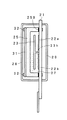
図1は、この実施の形態の傾斜センサの傾斜検出素子の分解斜視図である。また、図2は、この実施の形態の傾斜センサの傾斜検出素子を、その正面に垂直な面で切断した場合の断面図を示すものである。
【0042】
これらの図において、21はプリント基板で、例えばガラス布基材エポキシ樹脂積層板等の耐熱性部材からなる。このプリント基板21は、傾斜センサが傾斜検出対象物に取り付けられる時に、傾斜測定の基準面に対して垂直に配置される。図1では、この基準面は、二点鎖線で示す仮想線L0を含む面として示した。この基準面が、被測定面となる。この場合、傾斜角が0度とは、基準面が重力方向に垂直な線を含む状態である。
【0043】
このプリント基板21には、1対の差動電極22a,22bが、銅泊パターンによって、基準面に平行な面(プリント基板21面と垂直な面)と、プリント基板21との交差線(図1で二点鎖線で示す仮想線L2)により上下に分割される領域に、互いに電気的に独立に形成される。
【0044】
プリント基板21の差動電極22a,22bが形成される面とは反対側の面には、後述する傾斜センサの信号処理回路部が、プリント配線パターンと必要な電子部品とによって構成されて設けられる。差動電極22a,22bのそれぞれは、図1の電極点22c,22dからスルーホールを介してプリント基板21の信号処理回路部が形成される面の銅泊パターンに接続されるようにされている。
【0045】
そして、1対の差動電極22a,22bは、前記仮想線L2を対称軸として線対称な形状の電極パターンとして設けられる。また、この1対の差動電極22a,22bのそれぞれは、仮想線L2に垂直(したがって、基準面に垂直)な仮想線L1を対称軸とした線対称な電極パターン形状ともされる。図1の例の場合には、差動電極22a,22bの形状は縦置きの扇形に構成されている。
【0046】
図1の例の場合、差動電極22aおよび22bの円弧状周縁は、仮想線L1と仮想線L2との交点を中心とした円の一部の円弧とされている。この実施の形態の場合、その円の直径は、例えば14mmとされている。
【0047】
この場合、各差動電極22a,22bの扇形の開き角sは、傾斜センサの出力信号について、傾斜変化に対してリニアな出力特性を得たい傾斜角度範囲に応じて設定される。すなわち、傾斜角が0度の位置からの傾斜角度が所定値θa以上の範囲の出力特性をリニアにする場合には、開き角sは、s=(90−θa)×2に選定される。この例では、傾斜角が0度の位置からの傾斜角度が40度以上の範囲の出力特性をリニアにするために、100度とされている。
【0048】
23は共通電極板で、適当な剛性を持つ導電性部材で形成されている。この共通電極板23の形状は、1対の差動電極22a,22bに、この共通電極板を重ねたときに丁度一致するような、瓢箪型の形状とされている。
【0049】
この共通電極板23は、この板23と一体で、この板23から直角に曲げられた、この例では2個の端子23a,23bが、プリント基板21に設けられている端子孔24a,24bに挿入され、プリント基板21の信号処理回路部が形成される面において半田付け固定されることにより、図2に示すように、差動電極22a,22bに対して一定の間隔を持って平行に保持される状態でプリント基板21に取り付けられる。
【0050】
この例では、図1に示すように、より小型にするために、共通電極板23から導出される2個の端子23a,23bは、瓢箪型形状のくびれた部分から導出され、差動電極22aと22bとの間の電極パターンが形成されていないプリント基板21部分に設けられた端子孔24a,24bに挿入されるようにされている。これにより、傾斜検出素子の水平方向の大きさを小さくすることができる。
【0051】
25はオイルケースで、適当な柔軟性を有するプラスチックからなる。このケース25は、図2に示すように、断面がコ字状を有し、その端面がプリント基板21に、例えば両面テープ25Bなどの接着手段により接着されることにより、プリント基板21と共に密閉空間を形成する。
【0052】
このとき、差動電極22a,22bと共通電極23とケース25の対向面はそれぞれ平行になるように構成されるとともに、共通電極23の重心位置とケース25の重心位置とが一致するようにされている。
【0053】
そして、ケース25とプリント基板21とに形成される密閉空間内には、プリント基板21の差動電極22aに設けられた貫通孔26aからシリコン・オイル等の誘電性液体27が、密閉空間内の有効容積のほぼ1/2のレベル、すなわち図1の仮想線L2のレベルまで充填される。
【0054】
プリント基板21の差動電極22aの部分に設けられている貫通孔26aは、誘電性液体27が密閉空間内に封入された後、プリント基板21の信号処理回路部が設けられている面側から半田により穴埋めされて封止される。貫通孔26aは、銅泊パターン部分であるため、半田により容易に穴埋めされる。
【0055】
なお、この実施の形態では、後述する傾斜センサ出力のリニアな特性部分を補償するために、差動電極22aと対の差動電極22bにも、貫通孔26bが設けられ、前述と同様にして、半田により穴埋めされる。この場合、貫通孔26aと26bとは、同一径とされ、また、仮想線L2を対称軸として対称な位置に設けられる。
【0056】
なお、この実施の形態の場合の密閉空間のプリント基板21からの高さは、例えば3mmと薄く、プリント基板21と共通電極板23との距離は、1.5mm程度しかない。誘電性液体27は、例えば注射針のようなノズルを密閉空間内に差し込んで注入するが、1.5mmでは、差し込む距離として短すぎる。そこで、この実施の形態では、図1に示すように、差動電極22a,22bの貫通孔26a,26bの位置に対応する共通電極板23の位置には、同一径の貫通孔23c,23dが設けられ、誘電性液体27の注入用のノズルの差し込み距離として、3mmを確保できるようにしている。
【0057】
この場合、共通電極板23の貫通孔23cおよび23bは、仮想線L2を対称軸として線対称の位置となるので、後述する傾斜センサ出力のリニアな特性部分を補償することが可能となる。
【0058】
また、この実施の形態の場合、電極点22c,22dが形成されるスルーホールの一方、図の例では、電極点22cの部分は、誘電性液体27を封入するときの空気抜きにも用いられる。前述と同様に、後述する傾斜センサ出力のリニアな特性部分を補償するために、電極点22c,22dが形成されるスルーホールは、差動電極22a,22bにおいて、仮想線L2に対して対称な位置に設けられている。そして、これら電極点22c、22dは、誘電性液体を封入した後に、半田で封止される。
【0059】
28及び29は、外部の影響を遮断するための静電シールド板で、静電シールド板28は、ケース25およびその周辺を覆うように、プリント基板21に取り付けられ、静電シールド板29は、後述する信号処理回路部分を覆うようにプリント基板21に取り付けられる。
【0060】
また、この実施の形態の場合、オイルケース25の外平面には、導電性板31が取り付けられる。この導電性板31は、導電性の取り付けピン32により、オイルケース25を貫通してプリント基板21に固定されて取り付けられる。そして、導電性の取り付けピン32の先端は、プリント基板21の接地導体に接続されることにより、導電性板31が電気的に接地されている。
【0061】
なお、この例では、オイルケース25の端面が当接するプリント基板21の両面テープ25Bが張り付けられる部分は、表面を平坦にするために、オイルケース25の端面に対応する形状に銅泊パターンが形成されている。この銅泊パターンは、プリント基板25の裏面側のアースパターンに、ピン32が挿入される孔を介して接続されて、接地されている。
【0062】
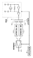
図3は、この実施の形態の傾斜センサの信号処理回路部分の構成を示すものである。
【0063】
この実施の形態の傾斜センサにおいては、入力端子41を通じてクロック信号SCが入力される。図3においては、このクロック信号SCは、傾斜センサとは別の制御回路基板に設けられる制御回路50から供給される。
【0064】
入力端子41を通じて入力された一定周波数のクロック信号は、例えばC−MOSインバータからなるクロックバッファ42により、波形整形され、これにより、入力クロック信号の波形のなまりが補正される。このクロックバッファ42の出力端子が、前述した図1および図2で説明した実施の形態の傾斜検出素子40の共通電極板23に接続される。また、傾斜検出素子40の1対の差動電極22a,22bのそれぞれは、容量−電圧変換回路43a,43bの入力端子に接続される。
【0065】
これら容量−電圧変換回路43aおよび43bの出力端子は、それぞれ差動増幅回路44の一方および他方の入力端子に接続される。この差動増幅回路44からは傾斜センサの出力端子45が導出される。
【0066】
なお、図3では、省略したが、この信号処理回路部は、図7の従来の電源安定化回路は設けられず、外部からの安定化された電源電圧が供給される構成とされている。
【0067】
この実施の形態の信号処理回路部は、上述のように構成されているので、入力端子41を通じて入力されたクロック信号SCは、クロックインバータ42により波形整形された後、差動電極22aと共通電極板23とで構成される第1のコンデンサを通じて容量−電圧変換回路43aに供給されると共に、差動電極22bと共通電極板23とで構成される第2のコンデンサを通じて容量−電圧変換回路12bに供給される。このとき、容量−電圧変換回路43aおよび43bのそれぞれには、第1のコンデンサの容量値Caおよび第2のコンデンサの容量値Cbのそれぞれに応じた波高値の信号が、それぞれ入力される。
【0068】
容量−電圧変換回路43aおよび43bは、それぞれの入力信号を整流し、平滑した電圧を出力する。したがって、容量−電圧変換回路43aおよび43bの出力電圧は、それぞれ回路43aおよび回路43bの入力信号の波高値、すなわち、第1のコンデンサの容量値Caおよび第2のコンデンサの容量値Cbのそれぞれに応じた大きさとなる。
【0069】
したがって、差動増幅回路44からは、容量−電圧変換回路43aの出力電圧と、容量−電圧変換回路43bの出力電圧との差の電圧が得られ、それが傾斜センサの出力として、出力端子45に導出される。
【0070】
この出力端子45に得られる傾斜センサの出力電圧は、制御回路50に供給される。この制御回路50は、この例では、マイクロコンピュータの構成とされており、CPU51に対して、システムバス52を通じてプログラムROM53、ワークエリアRAM54、およびI/Oポート55、56、57等を備える。
【0071】
制御回路50は、I/Oポート56を通じてクロック信号SCを傾斜センサの入力端子41に供給する。そして、傾斜センサの出力端子45からの傾斜検出出力としての出力電圧が、図示を省略したA/Dコンバータを通じて制御回路50のI/Oポート55に入力される。
【0072】
制御回路50では、プログラムROM52に格納された傾斜閾値検出プログラムに従って、傾斜センサの出力電圧が、所定の閾値電圧を超えたか否か検出し、前記閾値電圧を超えたことを検出したときには、被制御部60に、対応する制御信号を供給して所定の制御を実行させる。
【0073】
以上のような構成の傾斜検出素子40および信号処理回路部を備える傾斜センサを、前述したように傾斜測定の基準面となる被測定面上に設置し、制御回路50にその入力端子41および出力端子45を前述のように接続する。このとき、傾斜検出素子40のプリント基板1面が、被測定面の被測定傾斜方向を含む面となるように設置するのは、前述の場合と同様である。
【0074】
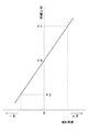
被測定面が、前記被測定傾斜方向に傾斜していない傾斜角が0の位置にあるとき(すなわち、重力方向に垂直な線を含む面となっているとき)、差動電極22bの部分は、その全体が誘電性液体27内にあり、一方、差動電極22aは、誘電性液体27には全く浸漬されていない状態になる。
【0075】
したがって、誘電体液体との浸漬量に応じた可変容量としての、差動電極22bと共通電極板23とで構成される第2のコンデンサの容量値Cbは、最大値となり、一方、差動電極22aと共通電極板23とで構成される第1のコンデンサの容量値Caは、最小値となる。
【0076】
したがって、容量−電圧変換回路43aと43bの出力電圧の差は最大となり、傾斜センサの出力電圧は、図4に示すように最大値Vmを示す。
【0077】
そして、被測定面が、前記被測定傾斜方向に傾斜したときであっても、その傾斜角度が、基準面に対して、扇形の差動電極22a,22bの開き角sに応じた角度K=90−s/2を超えない角度の範囲、この例では40度を超えない角度範囲では、差動電極22bは、ほぼ全部が誘電性液体27に浸漬した状態を維持し、一方、差動電極22aは、ほぼ誘電性液体27には浸漬されていない状態を維持する。
【0078】
したがって、第1のコンデンサの容量値Caと、第2のコンデンサの容量値Cbは、殆ど変化せず、差動増幅器44の出力電圧は、ほぼ電圧Vmのままとなる。
【0079】
そして、被測定面が、前記被測定傾斜方向にさらに傾斜して、前記角度Kを超えたときには、傾斜方向が+θ方向または−θ方向のいずれの傾斜方向の場合であっても、それまでほぼ全てが誘電性液体27内に浸漬されていた差動電極22bの一部が誘電性液体27の液面から露呈し、その分、差動電極22aの一部が誘電性液体27に浸漬する状態になる。
【0080】
そのため、差動電極22aと共通電極23とで形成される第1のコンデンサの容量値Caは、それまでよりも大きくなり、一方、差動電極22bと共通電極23とで形成される第2のコンデンサの容量値Cbは、それまでよりも小さくなる。
【0081】
したがって、容量−電圧変換回路43aの出力電圧と、容量−電圧変換回路43bの出力電圧との差が小さくなる。このため、傾斜センサの出力電圧は、図4に示すように、傾斜方向が+θ方向または−θ方向のいずれの場合であっても、傾斜角度の増加に応じてリニア(直線的)に下がるようになる。
【0082】
したがって、制御回路50で、検出する閾値の傾斜角θthに応じた単一の電圧Vthを予め定め、傾斜センサの出力電圧が、その電圧Vth以下になったか否かを検出することにより、傾斜方向が+θ方向または−θ方向のいずれの場合であっても、被測定面が閾値の傾斜角θthよりも傾いたか否かを検出することができる。
【0083】
この場合、制御回路50では、単一の電圧Vthを超えたか否かを監視するソフトウエアプログラムにより、被測定面が閾値の傾斜角θthよりも傾いたか否かを検出することができるので、従来の2つの閾値電圧を監視する場合に比べて、簡単なソフトウエアプログラムで良いという効果がある。
【0084】
制御回路50をマイクロコンピュータで構成するのではなく、デスクリートのハードウエア構成とすることもできるが、その場合には、単一の閾値電圧Vthを超えたか否かを検出する回路のみを構成するだけでよいので、従来のように、傾斜方向が+θ方向の閾値を超えたか否かの検出回路と、傾斜方向が−θ方向の閾値を超えたか否かの検出回路とを、2個設ける必要がなくなり、構成を簡略化することができる。
【0085】
また、上述の実施の形態の場合には、従来のような発振器を傾斜センサの信号処理回路に設けることなく、クロック信号を外部から供給するようにした構成であるので、プリント基板を含めて、全体の大きさを小さくすることができる。また、従来の電源安定化回路を削除するようにしたことも、傾斜センサの小型化に寄与している。
【0086】
なお、図3の例の場合には、容量−電圧変換回路43aの出力電圧を差動増幅回路44の非反転入力端子に供給し、容量−電圧変換回路43bの出力電圧を差動増幅回路44の反転入力端子に供給するようにしたので、差動増幅回路44の出力電圧の特性は、図4に示すような特性となるが、容量−電圧変換回路43aおよび43bの出力電圧の、差動増幅回路44の入力端子への入力を図3の場合と逆にすれば、差動増幅回路44の出力電圧の特性は、図4の場合とは逆となる。
【0087】
すなわち、第1のコンデンサの容量Caと第2のコンデンサCbの容量の差が最大の時に、出力電圧が最小になり、容量の差が小さくなるに連れて、出力電圧が増加するような特性となる。この場合には、閾値電圧Vthよりも大きくなることを検出することにより、被測定面が閾値の傾斜角θthよりも傾いたか否かを検出することができる
【0088】
【発明の効果】
以上説明したように、この発明の傾斜センサによれば、被測定面が、傾斜していない状態から時計方向、反時計方向のいずれの方向に傾斜しても、その傾斜の方向に関係なく、一定方向に変化する出力電圧を得ることができるので、検出する傾斜角に対応する閾値電圧がひとつでよく、所定の傾斜角以上に傾斜したか否かの検出回路を簡単な構成のものとすることができる。
【図面の簡単な説明】
【図1】この発明による傾斜センサの実施の形態の分解図である。
【図2】実施の形態の傾斜センサの断面図である。
【図3】実施の形態の傾斜センサの信号処理回路部の構成を説明するための図である。
【図4】実施の形態の傾斜センサの出力電圧特性を示す図である。
【図5】従来の傾斜センサの一例の分解図である。
【図6】従来の傾斜センサの一例の断面図である。
【図7】従来の傾斜センサの信号処理回路部の構成を示す図である。
【図8】従来の傾斜センサの出力電圧特性を示す図である。
【符号の説明】
21 プリント基板
22a,22b 差動電極
23 共通電極
25 オイルケース
27 誘電性液体
41 傾斜センサの入力端子
42 クロックバッファ
43a,43b 容量−電圧変換回路
44 差動増幅器[0001]
BACKGROUND OF THE INVENTION
The present invention detects, for example, an inclination angle with respect to a plane perpendicular to the direction of gravity, and when the detected inclination angle exceeds a predetermined value, it is suitable for issuing an alarm or performing a predetermined control. The present invention relates to a capacitance type inclination sensor.
[0002]
[Prior art]
As this type of capacitance type tilt sensor, for example, one using a tilt detecting element having a structure as shown in FIGS. 5 and 6 is known (for example, Japanese Utility Model Publication No. 4-53528, Japanese Utility Model Publication 5-). 14168).
[0003]
FIG. 5 is an exploded perspective view of the tilt detection element of the tilt sensor of this example. FIG. 6 shows a cross-sectional view of the tilt detection element taken along a plane perpendicular to the front face thereof.
[0004]
In these figures,
[0005]
In this printed
[0006]
A signal processing circuit section of an inclination sensor, which will be described later, is configured by a printed wiring pattern and necessary electronic components on the surface opposite to the surface on which the differential electrodes 2a and 2b of the printed
[0007]
The pair of differential electrodes 2a and 2b are provided as electrode patterns having a shape that is line-symmetric with respect to the virtual line L1. Each of the pair of differential electrodes 2a and 2b has a line-symmetric electrode pattern shape with a virtual line L2 perpendicular to the virtual line L1 as an axis of symmetry. In the case of the example of FIG. 5, the shape of the differential electrodes 2a and 2b is configured in a horizontal fan shape.
[0008]
In the example of FIG. 5, the arc-shaped peripheral edges of the differential electrodes 2a and 2b are a partial arc of a circle centered on the intersection of the virtual line L1 and the virtual line L2. In the case of this example, the diameter of the circle is 30 mm.
[0009]
[0010]
[0011]
In this case, the peripheral edge of the differential electrodes 2a and 2b, the peripheral edge of the
[0012]
In the sealed space formed by the
[0013]
The
[0014]
[0015]
FIG. 7 shows the configuration of the signal processing circuit portion of the tilt sensor of this example.
[0016]
In FIG. 7,
[0017]
The output terminals of these capacitance-voltage conversion circuits 12a and 12b are connected to one and the other input terminals of the differential amplifier circuit 13, respectively. An
[0018]
Since the signal processing circuit section is configured as described above, an oscillation output signal having a constant frequency from the
[0019]
Capacitance-voltage conversion circuits 12a and 12b rectify each input signal and output a smoothed voltage. Therefore, the output voltages of the capacitance-voltage conversion circuits 12a and 12b have magnitudes corresponding to the peak values of the respective input signals, that is, the capacitance values of the first capacitor and the second capacitor.
[0020]
Therefore, the differential amplifier circuit 13 obtains a difference voltage between the output voltage of the capacitance-voltage conversion circuit 12a and the output voltage of the capacitance-voltage conversion circuit 12b, which is used as the output of the tilt sensor as the
[0021]
As described above, the inclination sensor including the
[0022]
In this specification, the measured inclination direction of the surface to be measured is the direction of movement of the normal of the surface to be measured when the surface to be measured is inclined in the direction of the inclination to be measured. This means a direction along a plane including all the normal lines of the surface to be measured at each tilt position when tilting sequentially in the direction of the tilt to be measured.
[0023]
If the measured surface is not inclined in the measured inclination direction (that is, when it is a surface including a line perpendicular to the direction of gravity), the
[0024]
When the measured surface is tilted in the measured tilt direction, the liquid level position of the
[0025]
At this time, in FIG. 5, when the surface to be measured is tilted in the + θ direction (for example, counterclockwise) from the position where the tilt angle is 0 degree, the capacitance value of the first capacitor is decreased, and the second capacitor Since the capacitance value increases, the output voltage of the capacitance-voltage conversion circuit 12a becomes larger than the output voltage of the capacitance-voltage conversion circuit 12b. Therefore, the output voltage of the differential amplifier circuit 13 changes so as to be larger than the voltage Vo by an amount corresponding to the inclination angle in the + θ direction.
[0026]
On the other hand, in FIG. 5, when the surface to be measured is tilted in the -θ direction (for example, clockwise) from the position where the tilt angle is 0 degree, the capacitance value of the second capacitor becomes small, and the capacitance of the first capacitor Since the value increases, the output voltage of the capacitance-voltage conversion circuit 12a becomes smaller than the output voltage of the capacitance-voltage conversion circuit 12b. Therefore, the output voltage of the differential amplifier circuit 13 changes so as to be smaller than the voltage Vo by an amount corresponding to the inclination angle in the −θ direction.
[0027]
Therefore, a voltage corresponding to the difference between the output voltages of the capacitance-voltage conversion circuits 12a and 12b, that is, the difference between the capacitance values of the two capacitors is obtained from the differential amplifier circuit 13 as an output voltage. As shown in FIG. 8, the output voltage of the differential amplifier circuit 13 is proportional to the inclination angle of the surface to be measured from the surface position of the inclination angle = 0 including the inclination direction from the surface position of the inclination angle = 0. The DC voltage changes linearly.
[0028]
In this case, the fan-shaped shapes of the differential electrodes 2a and 2b and the
[0029]
When this tilt sensor is used to warn of the tilt of the surface to be measured above a certain value, a threshold voltage is set for the output voltage of the differential amplifier circuit 13, and a warning is issued when the threshold voltage is exceeded. However, since the output characteristic of the conventional tilt sensor is a linear characteristic as shown in FIG. 8, the threshold voltage V1 corresponding to the threshold tilt angle in the tilt direction is + θ direction and the threshold value in the tilt direction is −θ direction. A threshold voltage V2 corresponding to the tilt angle is set.
[0030]
The alarm circuit includes a first detection circuit that issues an alarm when the output voltage of the differential amplifier circuit 13 is greater than the voltage V1 when the tilt direction of the surface to be measured is the + θ direction, and the tilt direction is In the case of the −θ direction, the second detection circuit is configured to issue an alarm when the output voltage of the differential amplifier circuit 13 becomes smaller than the voltage V2.
[0031]
[Problems to be solved by the invention]
As described above, for example, when an alarm circuit is configured using a conventional tilt sensor, different threshold voltages are set depending on the difference in tilt direction between the + θ direction and the −θ direction from the surface position where the tilt angle = 0. There is a problem that the setting of the detection circuit requires different detection circuits, which complicates the configuration of the alarm circuit.
[0032]
In view of the above points, the present invention is capable of detecting a change in an inclination angle of a measured surface above a certain value with a single threshold regardless of the inclination direction from a position where the inclination angle is 0 degree. Is intended to provide.
[0033]
[Means for Solving the Problems]
In order to solve the above-mentioned problem, an inclination sensor according to the present invention provides:
A printed circuit board arranged in a direction perpendicular to a reference plane for tilt measurement;
A pair of differential electrodes provided electrically independent from each other on the printed circuit board;
A common electrode plate facing the pair of differential electrodes with a predetermined gap therebetween, and a common electrode attached to the printed circuit board by a terminal derived from the common electrode plate;
A case member configured to store the pair of differential electrodes and the common electrode plate in a sealed space formed between the printed circuit board and the printed circuit board;
A dielectric liquid encapsulated in a state in which the liquid level changes according to the inclination of the reference plane in the sealed space;
A signal which is provided on the printed circuit board and obtains an output signal having a level corresponding to a difference between capacitance values of two capacitors formed by the common electrode and each of the pair of differential electrodes as an inclination detection output. Processing circuit section
With
The pair of differential electrodes are provided electrically independently from each other in a region separated by a first intersection line between a plane parallel to the reference plane and the printed circuit board. Each of the pair of differential electrodes has a shape that is symmetrical with respect to a line as an axis of symmetry, and the shape of each of the pair of differential electrodes is based on a second intersection line between the plane perpendicular to the reference plane and the printed circuit board. A line-symmetric shape,
The dielectric liquid is sealed to a level of the first intersection line in the enclosed space;
The signal processing circuit sectionIs
PreviousA first capacitance-voltage conversion circuit that rectifies and converts a signal extracted through a first capacitor formed of the common electrode and one electrode of the pair of differential electrodes into a voltage;
A second capacitance-voltage conversion circuit that rectifies and converts a signal extracted through a second capacitor formed by the common electrode and the other electrode of the pair of differential electrodes into a voltage;
A differential amplifier circuit that outputs a difference between an output voltage of the first capacitance-voltage conversion circuit and an output voltage of the second capacitance-voltage conversion circuit;
KaraThe
A change in the tilt angle of the measured surface over a certain value regardless of the tilt direction, depending on whether the output of the differential amplifier circuit exceeds one threshold set for the output of the differential amplifier circuit. Detected
It is characterized by that.
[0034]
[Action]
When the inclination sensor according to the present invention having the above-described configuration is installed on the reference surface (surface to be measured) for inclination measurement so that the surface of the printed
[0035]
That is, if the measurement surface is not inclined in the measurement inclination direction, only one of the pair of differential electrodes is immersed in the dielectric liquid, and the output signal of the signal processing circuit unit is two It becomes a predetermined value Vn according to the difference between the capacitance values of the capacitors.
[0036]
When the measured surface is tilted in the measured tilt direction from this state, the tilt direction is within the range in which the tilt angle does not reach the other differential electrode of the pair of differential electrodes. The output signal of the signal processing circuit section is substantially the predetermined value Vn regardless of the above-described + θ direction or −θ direction.
[0037]
When the measured surface is further inclined in the measured inclination direction and the liquid level of the dielectric liquid reaches the other differential electrode of the pair of differential electrodes, the inclined direction Is in the above-described + θ direction or −θ direction in any of the inclined directions, a part of one differential electrode that has been immersed in the dielectric liquid until then is part of the liquid surface of the dielectric liquid. As a result, the part of the other differential electrode is immersed in the dielectric liquid.
[0038]
Then, the capacitance of the capacitor formed by one differential electrode and the common electrode, all of which were previously immersed in the dielectric liquid, becomes smaller, while part of the capacitor is immersed in the dielectric liquid. The capacitance of the capacitor formed by the other differential electrode and the common electrode is increased.
[0039]
Therefore, the difference between the capacitance values of the two capacitors becomes small, and therefore the level of the output signal from the signal processing circuit unit becomes small according to the inclination angle. At this time, the same change occurs regardless of whether the inclination direction is the above-described + θ direction or −θ direction.
[0040]
Therefore, according to the present invention, the threshold value when detecting an inclination of a predetermined inclination angle or more is only one in both the + θ direction and the −θ direction.
[0041]
DETAILED DESCRIPTION OF THE INVENTION
Embodiments of a tilt sensor according to the present invention will be described below with reference to the drawings.
FIG. 1 is an exploded perspective view of a tilt detecting element of the tilt sensor according to this embodiment. FIG. 2 is a cross-sectional view of the tilt detection element of the tilt sensor according to this embodiment, taken along a plane perpendicular to the front surface thereof.
[0042]
In these drawings,
[0043]
A pair of differential electrodes 22a and 22b is provided on the printed
[0044]
A signal processing circuit section of an inclination sensor, which will be described later, is configured by a printed wiring pattern and necessary electronic components on the surface of the printed
[0045]
The pair of differential electrodes 22a and 22b is provided as an electrode pattern having a line symmetry with the virtual line L2 as the axis of symmetry. Each of the pair of differential electrodes 22a and 22b has a line-symmetric electrode pattern shape with a virtual line L1 perpendicular to the virtual line L2 (and thus perpendicular to the reference plane) as an axis of symmetry. In the case of the example of FIG. 1, the shape of the differential electrodes 22 a and 22 b is configured in a vertical fan shape.
[0046]
In the case of the example of FIG. 1, the arc-shaped peripheral edges of the differential electrodes 22a and 22b are a partial arc of a circle centered on the intersection of the virtual line L1 and the virtual line L2. In the case of this embodiment, the diameter of the circle is, for example, 14 mm.
[0047]
In this case, the fan-shaped opening angle s of each differential electrode 22a, 22b is set according to the tilt angle range in which the output signal of the tilt sensor is desired to obtain linear output characteristics with respect to the tilt change. That is, when the output characteristics in the range where the tilt angle from the position where the tilt angle is 0 degrees is equal to or larger than the predetermined value θa are linear, the opening angle s is selected as s = (90−θa) × 2. In this example, in order to make the output characteristic in a range where the tilt angle from the position where the tilt angle is 0 degree is 40 degrees or more linear, it is set to 100 degrees.
[0048]
[0049]
The
[0050]
In this example, as shown in FIG. 1, in order to reduce the size, the two terminals 23a and 23b led out from the
[0051]
An
[0052]
At this time, the opposing surfaces of the differential electrodes 22a and 22b, the
[0053]
In the sealed space formed between the
[0054]
The through hole 26a provided in the differential electrode 22a portion of the printed
[0055]
In this embodiment, in order to compensate for the linear characteristic portion of the tilt sensor output described later, the differential electrode 22a and the pair of differential electrodes 22b are also provided with through holes 26b, which are the same as described above. The hole is filled with solder. In this case, the through holes 26a and 26b have the same diameter, and are provided at symmetrical positions with the virtual line L2 as the symmetry axis.
[0056]
Note that the height of the sealed space from the printed
[0057]
In this case, since the through holes 23c and 23b of the
[0058]
In the case of this embodiment, one of the through holes in which the electrode points 22c and 22d are formed, in the illustrated example, the portion of the electrode point 22c is also used for air venting when the
[0059]
28 and 29 are electrostatic shield plates for blocking external influences. The
[0060]
In this embodiment, a
[0061]
In this example, a portion of the printed
[0062]
FIG. 3 shows the configuration of the signal processing circuit portion of the tilt sensor of this embodiment.
[0063]
In the tilt sensor of this embodiment, the clock signal SC is input through the input terminal 41. In FIG. 3, the clock signal SC is supplied from a
[0064]
The constant frequency clock signal input through the input terminal 41 is waveform-shaped by a clock buffer 42 made of, for example, a C-MOS inverter, and thereby the rounding of the waveform of the input clock signal is corrected. The output terminal of the clock buffer 42 is connected to the
[0065]
The output terminals of these capacitance-voltage conversion circuits 43a and 43b are connected to one and the other input terminals of the differential amplifier circuit 44, respectively. An
[0066]
Although not shown in FIG. 3, the signal processing circuit unit is not provided with the conventional power supply stabilization circuit of FIG. 7, but is configured to be supplied with a stabilized power supply voltage from the outside.
[0067]
Since the signal processing circuit unit of this embodiment is configured as described above, the clock signal SC input through the input terminal 41 is waveform-shaped by the clock inverter 42 and then the differential electrode 22a and the common electrode. The
[0068]
Capacitance-voltage conversion circuits 43a and 43b rectify each input signal and output a smoothed voltage. Therefore, the output voltages of the capacitance-voltage conversion circuits 43a and 43b are respectively applied to the peak values of the input signals of the circuits 43a and 43b, that is, the capacitance value Ca of the first capacitor and the capacitance value Cb of the second capacitor, respectively. It becomes the size according to.
[0069]
Therefore, the differential amplifier circuit 44 obtains a voltage difference between the output voltage of the capacitance-voltage conversion circuit 43a and the output voltage of the capacitance-voltage conversion circuit 43b, which is used as an output of the tilt sensor as an
[0070]
The output voltage of the tilt sensor obtained at the
[0071]
The
[0072]
The
[0073]
The tilt sensor having the
[0074]
When the measured surface is at a position where the inclination angle not inclined in the measured inclination direction is 0 (that is, the surface includes a line perpendicular to the gravity direction), the portion of the differential electrode 22b is The whole is in the
[0075]
Therefore, the capacitance value Cb of the second capacitor constituted by the differential electrode 22b and the
[0076]
Therefore, the difference between the output voltages of the capacitance-voltage conversion circuits 43a and 43b becomes the maximum, and the output voltage of the inclination sensor shows the maximum value Vm as shown in FIG.
[0077]
Even when the measured surface is tilted in the measured tilt direction, the tilt angle is an angle K = in accordance with the opening angle s of the sector-shaped differential electrodes 22a and 22b with respect to the reference surface. In an angle range not exceeding 90-s / 2, in this example, an angle range not exceeding 40 degrees, the
[0078]
Therefore, the capacitance value Ca of the first capacitor and the capacitance value Cb of the second capacitor hardly change, and the output voltage of the differential amplifier 44 remains substantially at the voltage Vm.
[0079]
When the measured surface further tilts in the measured tilt direction and exceeds the angle K, the tilt direction is almost the same until then, regardless of whether the tilt direction is the + θ direction or the −θ direction.
[0080]
Therefore, the capacitance value Ca of the first capacitor formed by the differential electrode 22a and the
[0081]
Therefore, the difference between the output voltage of the capacitance-voltage conversion circuit 43a and the output voltage of the capacitance-voltage conversion circuit 43b is reduced. For this reason, as shown in FIG. 4, the output voltage of the tilt sensor decreases linearly (in a straight line) as the tilt angle increases, regardless of whether the tilt direction is the + θ direction or the −θ direction. become.
[0082]
Therefore, the
[0083]
In this case, the
[0084]
The
[0085]
In the case of the above-described embodiment, since the clock signal is supplied from the outside without providing a conventional oscillator in the signal processing circuit of the tilt sensor, including the printed circuit board, The overall size can be reduced. In addition, the fact that the conventional power supply stabilization circuit is deleted also contributes to the downsizing of the tilt sensor.
[0086]
In the case of the example of FIG. 3, the output voltage of the capacitance-voltage conversion circuit 43a is supplied to the non-inverting input terminal of the differential amplification circuit 44, and the output voltage of the capacitance-voltage conversion circuit 43b is supplied to the differential amplification circuit 44. 4, the output voltage characteristics of the differential amplifier circuit 44 are as shown in FIG. 4, but the output voltages of the capacitance-voltage conversion circuits 43a and 43b are differentially output. If the input to the input terminal of the amplifier circuit 44 is reversed from that in FIG. 3, the output voltage characteristics of the differential amplifier circuit 44 are reversed from those in FIG.
[0087]
In other words, when the difference between the capacitance of the first capacitor Ca and the capacitance of the second capacitor Cb is maximum, the output voltage is minimized, and the output voltage increases as the difference in capacitance decreases. Become. In this case, it is possible to detect whether or not the measured surface is inclined with respect to the threshold inclination angle θth by detecting that the threshold voltage Vth is greater.
[0088]
【The invention's effect】
As described above, according to the tilt sensor of the present invention, regardless of the direction of the tilt, regardless of whether the surface to be measured is tilted in a clockwise direction or a counterclockwise direction from a non-tilted state, Since an output voltage that changes in a certain direction can be obtained, only one threshold voltage corresponding to the inclination angle to be detected is required, and the detection circuit for determining whether or not the inclination angle exceeds a predetermined inclination angle has a simple configuration. be able to.
[Brief description of the drawings]
FIG. 1 is an exploded view of an embodiment of a tilt sensor according to the present invention.
FIG. 2 is a cross-sectional view of the tilt sensor according to the embodiment.
FIG. 3 is a diagram for explaining a configuration of a signal processing circuit unit of the tilt sensor according to the embodiment.
FIG. 4 is a diagram illustrating output voltage characteristics of the tilt sensor according to the embodiment.
FIG. 5 is an exploded view of an example of a conventional tilt sensor.
FIG. 6 is a cross-sectional view of an example of a conventional tilt sensor.
FIG. 7 is a diagram illustrating a configuration of a signal processing circuit unit of a conventional tilt sensor.
FIG. 8 is a graph showing output voltage characteristics of a conventional tilt sensor.
[Explanation of symbols]
21 Printed circuit board
22a, 22b Differential electrode
23 Common electrode
25 Oil case
27 Dielectric liquid
41 Input terminal of tilt sensor
42 clock buffer
43a, 43b Capacitance-voltage conversion circuit
44 Differential Amplifier
Claims (2)
前記プリント基板上において、互いに電気的に独立に設けられる1対の差動電極と、
前記1対の差動電極に対して所定の空隙を隔てて対向する共通電極板を備え、この共通電極板から導出される端子により、前記プリント基板に取り付けられる共通電極と、
前記1対の差動電極と前記共通電極板とを、前記プリント基板との間で形成する密閉空間内に収納するようにするケース部材と、
前記密閉空間内に、液面が前記基準面の傾斜に応じて変化するような状態で封入された誘電性液体と、
前記プリント基板上に設けられ、前記共通電極と、前記1対の差動電極のそれぞれとで構成される2個のコンデンサの容量値の差分に応じたレベルの出力信号を傾斜検出出力として得る信号処理回路部と
を備え、
前記1対の差動電極は、前記基準面に平行な面と前記プリント基板との第1の交差線により分けられる領域に互いに電気的に独立に設けられるものであって、前記第1の交差線を対称軸として互いに線対称な形状であり、かつ、前記1対の差動電極のそれぞれの形状は、前記基準面に垂直な面と前記プリント基板との第2の交差線を対称軸として線対称な形状であり、
前記誘電性液体は、前記密閉空間内の前記第1の交差線のレベルまで封入され、
前記信号処理回路部は、
前記共通電極と前記1対の差動電極の一方の電極とで構成される第1のコンデンサを通じて取り出される信号を整流して電圧に変換する第1の容量−電圧変換回路と、
前記共通電極と前記1対の差動電極の他方の電極とで構成される第2のコンデンサを通じて取り出される信号を整流して電圧に変換する第2の容量−電圧変換回路と、
前記第1の容量−電圧変換回路の出力電圧と、前記第2の容量−電圧変換回路の出力電圧との差分を出力する差動増幅回路と
からなり、
前記差動増幅回路の出力に対して設定された1つの閾値を前記差動増幅回路の出力が超えたか否かにより、傾斜方向に関係なく、前記被測定面の一定値以上の傾斜角の変化を検出するようにした
ことを特徴とする傾斜センサ。A printed circuit board arranged in a direction perpendicular to a reference plane for tilt measurement;
A pair of differential electrodes provided electrically independent from each other on the printed circuit board;
A common electrode plate facing the pair of differential electrodes with a predetermined gap therebetween, and a common electrode attached to the printed circuit board by a terminal derived from the common electrode plate;
A case member configured to accommodate the pair of differential electrodes and the common electrode plate in a sealed space formed between the printed circuit board and the printed circuit board;
A dielectric liquid sealed in a state in which the liquid level changes in accordance with the inclination of the reference plane in the sealed space;
A signal which is provided on the printed circuit board and obtains an output signal having a level corresponding to a difference between capacitance values of two capacitors formed by the common electrode and each of the pair of differential electrodes as an inclination detection output. And a processing circuit section,
The pair of differential electrodes are provided electrically independently from each other in a region separated by a first intersection line between a plane parallel to the reference plane and the printed circuit board. Each of the pair of differential electrodes has a shape that is symmetrical with respect to a line as an axis of symmetry, and the shape of each of the pair of differential electrodes is based on a second intersection line between the plane perpendicular to the reference plane and the printed circuit board. A line-symmetric shape,
The dielectric liquid is sealed to a level of the first intersection line in the enclosed space;
The signal processing circuit unit is
A first capacitor for converting before Symbol voltage by rectifying the signal extracted through the first capacitor comprised of the one electrode of the common electrode and the pair of differential electrodes - voltage conversion circuit,
A second capacitance-voltage conversion circuit that rectifies and converts a signal extracted through a second capacitor formed by the common electrode and the other electrode of the pair of differential electrodes into a voltage;
Said first capacitor - the output voltage of the voltage conversion circuit, the second capacitor - a differential amplifier circuit for outputting a difference between the output voltage of the voltage converting circuit and Ri Tona,
A change in the tilt angle of the measured surface over a certain value regardless of the tilt direction, depending on whether the output of the differential amplifier circuit exceeds one threshold set for the output of the differential amplifier circuit. An inclination sensor characterized by detecting the above .
ことを特徴とする請求項1に記載の傾斜センサ。The tilt sensor according to claim 1.
Priority Applications (7)
| Application Number | Priority Date | Filing Date | Title |
|---|---|---|---|
| JP2000048559A JP3659855B2 (en) | 2000-02-25 | 2000-02-25 | Tilt sensor |
| TW090103701A TW522221B (en) | 2000-02-25 | 2001-02-19 | Tilting detector |
| ES200100372A ES2170034A1 (en) | 2000-02-25 | 2001-02-19 | Tilt sensor |
| IT2001TO000155A ITTO20010155A1 (en) | 2000-02-25 | 2001-02-21 | INCLINATION SENSOR. |
| US09/790,657 US6442855B2 (en) | 2000-02-25 | 2001-02-23 | Tilt sensor |
| CNB011190272A CN1307403C (en) | 2000-02-25 | 2001-02-25 | Inclination sensor |
| US10/231,214 US20030000095A1 (en) | 2000-02-25 | 2002-08-30 | Tilt sensor |
Applications Claiming Priority (1)
| Application Number | Priority Date | Filing Date | Title |
|---|---|---|---|
| JP2000048559A JP3659855B2 (en) | 2000-02-25 | 2000-02-25 | Tilt sensor |
Publications (2)
| Publication Number | Publication Date |
|---|---|
| JP2001235325A JP2001235325A (en) | 2001-08-31 |
| JP3659855B2 true JP3659855B2 (en) | 2005-06-15 |
Family
ID=18570629
Family Applications (1)
| Application Number | Title | Priority Date | Filing Date |
|---|---|---|---|
| JP2000048559A Expired - Fee Related JP3659855B2 (en) | 2000-02-25 | 2000-02-25 | Tilt sensor |
Country Status (6)
| Country | Link |
|---|---|
| US (2) | US6442855B2 (en) |
| JP (1) | JP3659855B2 (en) |
| CN (1) | CN1307403C (en) |
| ES (1) | ES2170034A1 (en) |
| IT (1) | ITTO20010155A1 (en) |
| TW (1) | TW522221B (en) |
Families Citing this family (18)
| Publication number | Priority date | Publication date | Assignee | Title |
|---|---|---|---|---|
| US6625896B1 (en) * | 2001-06-11 | 2003-09-30 | The United States Of America As Represented By The Secretary Of The Navy | Electrolytic tilt sensor and method for manufacturing same |
| US6688013B2 (en) * | 2001-12-13 | 2004-02-10 | The Fredericks Company | Electrolytic-tilt-sensor |
| US7024947B2 (en) | 2002-03-07 | 2006-04-11 | Alps Electric Co., Ltd. | Detection device including circuit component |
| JP4350600B2 (en) * | 2003-10-31 | 2009-10-21 | 株式会社東海理化電機製作所 | Capacitive tilt angle sensor |
| US7190278B2 (en) * | 2004-03-08 | 2007-03-13 | Nuvo Holdings, Llc | Asset tag with event detection capabilities |
| US7088258B2 (en) * | 2004-03-08 | 2006-08-08 | Nuvo Holdings, Llc | Tilt sensor apparatus and method therefor |
| JP4033183B2 (en) * | 2004-09-22 | 2008-01-16 | オムロン株式会社 | Tilt sensor |
| JP4465607B2 (en) * | 2004-12-27 | 2010-05-19 | 東洋電装株式会社 | Tilt sensor |
| US7254897B2 (en) * | 2005-04-13 | 2007-08-14 | Kavlico Corporation | Integrated tilt sensor |
| US7370429B2 (en) * | 2006-08-29 | 2008-05-13 | Hall Floyd E | Integrated electronic level device |
| KR100924260B1 (en) * | 2008-12-08 | 2009-10-30 | 노익환 | Inclination sesning apparatus and apparatus for controlling posture automatically using same |
| CN102042823B (en) * | 2009-10-26 | 2014-02-26 | 北京信息科技大学 | Inclination angle measuring device and measuring method thereof |
| TWI454664B (en) * | 2012-09-27 | 2014-10-01 | Sagatek Co Ltd | A liquid multilayer capacitive micro inclinometer |
| US9146104B2 (en) * | 2012-12-31 | 2015-09-29 | Virgina Tech Intellectual Properties, Inc. | Jellyfish-inspired tilt sensor and artificial mesoglea |
| CN104748812B (en) * | 2015-03-28 | 2023-06-27 | 智恒(厦门)微电子有限公司 | Differential capacitance small object counting sensor |
| US10536356B2 (en) * | 2015-09-21 | 2020-01-14 | Splunk Inc. | Generating and displaying topology map time-lapses of cloud computing resources |
| TWI666540B (en) * | 2017-04-12 | 2019-07-21 | 緯創資通股份有限公司 | Gravity center adjustment mechanism and related camera device |
| CN110851004B (en) * | 2019-11-19 | 2023-10-27 | 合肥京东方光电科技有限公司 | Touch pen, driving method thereof and touch system |
Family Cites Families (18)
| Publication number | Priority date | Publication date | Assignee | Title |
|---|---|---|---|---|
| US3906471A (en) * | 1973-09-12 | 1975-09-16 | Sun Oil Co Pennsylvania | High side meter |
| WO1983001304A1 (en) * | 1981-10-02 | 1983-04-14 | Wiklund, Klas, Rudolf | Electronic levelling cell |
| EP0117226A3 (en) * | 1983-01-28 | 1985-10-02 | Max Engler | Apparatus for measuring deviations from the vertical and its use |
| DD226068A1 (en) * | 1984-05-28 | 1985-08-14 | Suhl Feinmesszeugfab Veb | CAPACITIVE TILT AND LEVEL MEASUREMENT DEVICE |
| US4642555A (en) * | 1985-01-31 | 1987-02-10 | Sperry Corporation | Differential capacitance detector |
| US4644662A (en) * | 1985-01-31 | 1987-02-24 | Sperry Corporation | Capacitive gravity sensor |
| JPS649309A (en) * | 1987-07-01 | 1989-01-12 | Agency Ind Science Techn | Electrostatic capacitance type angle of inclination sensor |
| US4811491A (en) * | 1987-09-04 | 1989-03-14 | Etak, Inc. | Two-axis differential capacitance inclinometer |
| DE69027851T2 (en) * | 1989-03-21 | 1997-03-20 | Zircon Int Inc | ELECTRONIC CONDENSER LEVEL WITH AUTOMATIC ELECTRODE SELECTION |
| US5014795A (en) * | 1989-05-01 | 1991-05-14 | Augers Unlimited, Inc. | Percent grade boring and monitoring apparatus |
| JPH0453528A (en) | 1990-06-20 | 1992-02-21 | Toshiba Corp | Data collection method in mri apparatus |
| DE4106932A1 (en) * | 1991-03-05 | 1992-09-10 | Bosch Gmbh Robert | INCLINATION SENSOR |
| JPH0514168A (en) | 1991-07-02 | 1993-01-22 | Fujitsu Ltd | Output circuit and semiconductor integrated circuit device |
| US5237753A (en) * | 1992-05-18 | 1993-08-24 | Lucas Sensing Systems, Inc. | Capacitive gravity sensor and inclinometer |
| US5802728A (en) * | 1995-08-17 | 1998-09-08 | Watson Industries, Inc. | Liquid level and angle detector |
| JPH10160458A (en) * | 1996-12-03 | 1998-06-19 | Toyota Motor Corp | Tilt sensor |
| JP3622505B2 (en) * | 1998-02-02 | 2005-02-23 | オムロン株式会社 | Tilt sensor |
| JP4014326B2 (en) * | 1999-02-18 | 2007-11-28 | 本田技研工業株式会社 | Capacitive tilt sensor |
-
2000
- 2000-02-25 JP JP2000048559A patent/JP3659855B2/en not_active Expired - Fee Related
-
2001
- 2001-02-19 ES ES200100372A patent/ES2170034A1/en active Pending
- 2001-02-19 TW TW090103701A patent/TW522221B/en not_active IP Right Cessation
- 2001-02-21 IT IT2001TO000155A patent/ITTO20010155A1/en unknown
- 2001-02-23 US US09/790,657 patent/US6442855B2/en not_active Expired - Fee Related
- 2001-02-25 CN CNB011190272A patent/CN1307403C/en not_active Expired - Fee Related
-
2002
- 2002-08-30 US US10/231,214 patent/US20030000095A1/en not_active Abandoned
Also Published As
| Publication number | Publication date |
|---|---|
| CN1307403C (en) | 2007-03-28 |
| US6442855B2 (en) | 2002-09-03 |
| TW522221B (en) | 2003-03-01 |
| ITTO20010155A1 (en) | 2002-08-21 |
| JP2001235325A (en) | 2001-08-31 |
| CN1320808A (en) | 2001-11-07 |
| ES2170034A1 (en) | 2002-07-16 |
| ITTO20010155A0 (en) | 2001-02-21 |
| US20010045019A1 (en) | 2001-11-29 |
| US20030000095A1 (en) | 2003-01-02 |
Similar Documents
| Publication | Publication Date | Title |
|---|---|---|
| JP3659855B2 (en) | Tilt sensor | |
| US5433110A (en) | Detector having selectable multiple axes of sensitivity | |
| US5172481A (en) | Electronic inclinometer | |
| JPS60169719A (en) | Physical quantity detecting apparatus | |
| KR20060113468A (en) | Angular velocity sensor | |
| US5942685A (en) | Acceleration sensor | |
| ES2440479T3 (en) | Integrated tilt detector | |
| JP4365982B2 (en) | Tilt sensor | |
| JP4386519B2 (en) | Tilt detection unit | |
| JP3269269B2 (en) | Vibration detection sensor | |
| JP2732413B2 (en) | Acceleration sensor | |
| JPH06275935A (en) | Circuit pattern in flexible board | |
| JPH1078485A (en) | Earthquake wave detector | |
| JPH0728732Y2 (en) | Oscillator | |
| JP2530766Y2 (en) | Structure to prevent electrostatic breakdown of electronic equipment | |
| JPH09260948A (en) | Crystal oscillator | |
| JPH0231713Y2 (en) | ||
| JPH084565Y2 (en) | Capacitive tilt sensor assembly structure | |
| CN111487446A (en) | Electronic measuring device | |
| JPH1140021A (en) | Electrostatic capacity proximity sensor | |
| JPH11316104A (en) | Magnetoresistance element | |
| JP2000221208A (en) | Capacitance type acceleration sensor | |
| JP2020027906A (en) | Board mounting structure, mounting board, and voltage measurement unit | |
| JPH0538516U (en) | Tilt sensor | |
| JPH06318839A (en) | Piezoelectric component incorporating capacitor |
Legal Events
| Date | Code | Title | Description |
|---|---|---|---|
| A977 | Report on retrieval |
Free format text: JAPANESE INTERMEDIATE CODE: A971007 Effective date: 20041129 |
|
| A131 | Notification of reasons for refusal |
Free format text: JAPANESE INTERMEDIATE CODE: A131 Effective date: 20041208 |
|
| A521 | Request for written amendment filed |
Free format text: JAPANESE INTERMEDIATE CODE: A523 Effective date: 20050202 |
|
| TRDD | Decision of grant or rejection written | ||
| A01 | Written decision to grant a patent or to grant a registration (utility model) |
Free format text: JAPANESE INTERMEDIATE CODE: A01 Effective date: 20050302 |
|
| A61 | First payment of annual fees (during grant procedure) |
Free format text: JAPANESE INTERMEDIATE CODE: A61 Effective date: 20050315 |
|
| R150 | Certificate of patent or registration of utility model |
Free format text: JAPANESE INTERMEDIATE CODE: R150 |
|
| FPAY | Renewal fee payment (event date is renewal date of database) |
Free format text: PAYMENT UNTIL: 20090325 Year of fee payment: 4 |
|
| FPAY | Renewal fee payment (event date is renewal date of database) |
Free format text: PAYMENT UNTIL: 20090325 Year of fee payment: 4 |
|
| FPAY | Renewal fee payment (event date is renewal date of database) |
Free format text: PAYMENT UNTIL: 20100325 Year of fee payment: 5 |
|
| LAPS | Cancellation because of no payment of annual fees |