JP3658331B2 - Recording / reproducing method of memory element, magnetoresistive element, and magnetic random access memory - Google Patents
Recording / reproducing method of memory element, magnetoresistive element, and magnetic random access memory Download PDFInfo
- Publication number
- JP3658331B2 JP3658331B2 JP2001078470A JP2001078470A JP3658331B2 JP 3658331 B2 JP3658331 B2 JP 3658331B2 JP 2001078470 A JP2001078470 A JP 2001078470A JP 2001078470 A JP2001078470 A JP 2001078470A JP 3658331 B2 JP3658331 B2 JP 3658331B2
- Authority
- JP
- Japan
- Prior art keywords
- magnetic layer
- magnetic
- layer
- magnetization
- memory
- Prior art date
- Legal status (The legal status is an assumption and is not a legal conclusion. Google has not performed a legal analysis and makes no representation as to the accuracy of the status listed.)
- Expired - Lifetime
Links
Images


Classifications
-
- B—PERFORMING OPERATIONS; TRANSPORTING
- B82—NANOTECHNOLOGY
- B82Y—SPECIFIC USES OR APPLICATIONS OF NANOSTRUCTURES; MEASUREMENT OR ANALYSIS OF NANOSTRUCTURES; MANUFACTURE OR TREATMENT OF NANOSTRUCTURES
- B82Y25/00—Nanomagnetism, e.g. magnetoimpedance, anisotropic magnetoresistance, giant magnetoresistance or tunneling magnetoresistance
-
- H—ELECTRICITY
- H01—ELECTRIC ELEMENTS
- H01F—MAGNETS; INDUCTANCES; TRANSFORMERS; SELECTION OF MATERIALS FOR THEIR MAGNETIC PROPERTIES
- H01F10/00—Thin magnetic films, e.g. of one-domain structure
- H01F10/32—Spin-exchange-coupled multilayers, e.g. nanostructured superlattices
- H01F10/324—Exchange coupling of magnetic film pairs via a very thin non-magnetic spacer, e.g. by exchange with conduction electrons of the spacer
- H01F10/3268—Exchange coupling of magnetic film pairs via a very thin non-magnetic spacer, e.g. by exchange with conduction electrons of the spacer the exchange coupling being asymmetric, e.g. by use of additional pinning, by using antiferromagnetic or ferromagnetic coupling interface, i.e. so-called spin-valve [SV] structure, e.g. NiFe/Cu/NiFe/FeMn
Landscapes
- Chemical & Material Sciences (AREA)
- Engineering & Computer Science (AREA)
- Crystallography & Structural Chemistry (AREA)
- Nanotechnology (AREA)
- Power Engineering (AREA)
- Measuring Magnetic Variables (AREA)
- Mram Or Spin Memory Techniques (AREA)
- Magnetic Heads (AREA)
- Thin Magnetic Films (AREA)
- Semiconductor Memories (AREA)
- Hall/Mr Elements (AREA)
Description
【0001】
【発明の属する技術分野】
本発明は、不揮発性固体メモリなどに使用される磁気抵抗素子に関し、特に、2重トンネル垂直磁化TMR素子である磁気抵抗素子と、この磁気抵抗素子を用いたメモリ素子及びメモリセルと、そのようなメモリ素子の記録再生方法に関する。
【0002】
【従来の技術】
近年、磁気抵抗素子を用いた磁気メモリが盛んに研究されている。この磁気メモリ素子を用いたメモリ装置として磁気ランダムアクセスメモリ(MRAM:Magnetic Random Access Memory)は、情報の保存に磁性膜を用いているため、電源を落としても情報が消えない、すなわち不揮発性であるという特徴を有している。
【0003】
MRAMのメモリセルには、スピントンネル効果による磁気抵抗素子が設けられている。この素子は、一般にTMR素子と呼ばれており、抵抗変化率(MR比)が従来の磁気抵抗素子と比較して大きく、抵抗値も数KΩから数十KΩとMRAMのメモリセルとして最適な値に設定することが可能なため、MRAMの記憶素子として一般的に用いられている。
【0004】
ところが、このTMR素子は、素子にかかるバイアス電圧が大きくなると、MR比が減少するという特性を持ち合わせている。例えば、数mVで50%近いMR比が得られているが、500mVで約20%になるといった報告がなされている。MRAMでは、数100mVのバイアス電圧がTMR素子に印加されるため、この減少率は無視できないレベルであり、検出感度を劣化させることになる。
【0005】
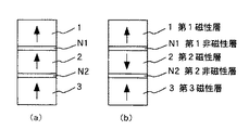
このTMR素子のMR比のバイアス電圧依存性の課題に対する対策案として、絶縁層を2個設けたTMR素子を用いることが提案されている。例えば、特開平9−260743号公報には、膜面内方向に磁化された磁性層を用いて、磁性層と絶縁層と磁性層と絶縁層と磁性層の積層構造により、トンネル接合膜を作成した素子が開示されている。図11は絶縁層を2つ有する従来のTMR素子の構成を示すものであり、(a)は二値の記録の一方に対応する磁化状態を示し、(b)は二値の記録の他方に対応する磁化状態を示している。図中、矢印は各磁性層の磁化の方向を示している。このTMR素子は、面内磁化膜である第1磁性層11、第1非磁性層N11、面内磁化膜である第2磁性層12、第2非磁性層N12及び面内磁化膜である第3磁性層13をこの順に積層したものであって、各磁性層11〜13の保磁力の差異を利用して、中央に位置する第2磁性層12の磁化方向を、より保磁力の高い第1磁性層11及び第3磁性層13の磁化方向に対して平行にするか(a)、あるいは反平行にするか(b)で、二値の情報を記憶し、また、これら2つの状態間でトンネル膜の抵抗値に差ができるようにして、記憶された情報を読み出せるようにする。
【0006】
このような絶縁層を2個設けたTMR素子は、通常のTMR素子を2個直列に接続するのと同じように、1つのトンネル障壁膜にかかるバイアス電圧が半減するため、MR比のバイアス電圧による劣化が小さくなるといった効果がある。
【0007】
【発明が解決しようとする課題】
しかしながら、図11に示した従来の磁気抵抗素子は、バイアス電圧依存性に対しては効果があるものの、素子サイズが小さくなると磁化状態が不安定になるといった課題が生じる。これは、磁気抵抗素子に面内磁化膜を用いているために生じ、特に図11の(a)に示す磁化状態の場合には、各磁性層の磁化が同じ方向を向くために、磁性膜の端面にある磁極による自己磁界(反磁界)が各層に印加され、各層の磁化状態がより不安定となる。このために、(a)に示す状態のように一方向に磁化配向させるためには、磁化容易軸方向に磁性膜を長くするといった素子形状の改良で対策を取ることが一般的である。これは、素子サイズが大きくなり、メモリセル面積の増加、すなわち、集積度の低下の原因となる。
【0008】
さらに、図11の(a),(b)の2つの状態のうち、(b)の状態は磁性層11〜13から出る磁束が閉じるため、エネルギー的に安定な状態である。しかし(a)の状態は、各磁性層11〜13の磁化が反発しあうため、エネルギー的に高い状態にあり不安定である。このため、磁化状態を(b)から(a)にするのに必要な磁界が、磁化状態を(a)から(b)にするのに必要な磁界よりも大きくなる。磁気メモリ素子において、情報の記録のために磁性膜の磁化を反転させるためには、書き込み線に電流を流してそこから発生する磁界を磁性膜に印加する。このため、反転磁界が大きくなると、書き込み線には大きな電流を流す必要があり、全体の消費電力が大きくなってしまう。また、磁化状態(a)は、エネルギー的に不安定であるため、熱などの影響で(b)の状態に変わりやすい特性を有する。このため、情報の安定性に欠けることとなる。
【0009】
これらの不安定性や反転磁界の問題は、素子サイズが小さくなるとより顕著になる傾向がある。したがって、従来提案された素子においては、集積度を高くしようとすると、磁化状態が不安定になったり、反転磁界が増加するといった課題があった。
【0010】
そこで本発明の目的は、磁化状態が安定であるとともに情報の記録を低消費電流で安定して行うことができる磁気抵抗素子と、このような磁気抵抗素子を用いたメモリ素子及びメモリセルと、これらのメモリ素子に対する記録再生方法とを提供することにある。
【0011】
【課題を解決するための手段】
上述した課題に鑑み、本発明者は、磁気抵抗素子を構成する磁性膜として反磁界エネルギーの小さい磁性膜を用い、さらに反平行磁化状態のときと平行磁化状態のときとでエネルギー的に差異の少ない媒体構成を用いることによって、上記課題を解決することを見出し、本発明を完成させた。
【0012】
すなわち上記の目的は、
(1)膜面垂直方向に磁化した第1磁性層と、第1非磁性層と、膜面垂直方向に磁化した第2磁性層と、第2非磁性層と、膜面垂直方向に磁化した第3磁性層とが順に積層され、第1磁性層及び第3磁性層の保磁力がいずれも第2磁性層の保磁力よりも小さい磁気抵抗素子を有するメモリ素子の記録再生方法であって、第2磁性層の磁化方向を記録情報に応じて変化させ、第1磁性層及び前記第3磁性層の磁化方向を読出し時に反転させるようにしたことを特徴とするメモリ素子の記録再生方法、及び、
(2)第1磁性層の磁化の向きと第3磁性層の磁化の向きが反平行である(1)に記載のメモリ素子の記録再生方法、及び、
(3)第1磁性層及び第3磁性層の一方が鉄族元素副格子磁化優勢な希土類鉄族合金膜であり、第1磁性層及び第3磁性層の他方が希土類元素副格子磁化優勢な希土類鉄族合金膜である、(2)に記載のメモリ素子の記録再生方法、及び、
(4)第1非磁性層及び第2非磁性層が絶縁層からなる(1)〜(3)に記載のメモリ素子の記録再生方法、及び、
(5)メモリ素子が基板上に複数配され、メモリ素子の少なくとも一つを選択して、情報の記録再生を行うことを特徴とする、(1)〜(4)に記載のメモリ素子の記録再生方法、及び、
(6)膜面垂直方向に磁化した第1磁性層と、第1非磁性層と、膜面垂直方向に磁化した第2磁性層と、第2非磁性層と、膜面垂直方向に磁化した第3磁性層とが順に積層され、第1磁性層と第1非磁性層の間、第2磁性層と第1非磁性層の間、第2磁性層と第2非磁性層の間、第2非磁性層と第3磁性層の間の少なくとも一つに、第1磁性層もしくは第2磁性層もしくは第3磁性層よりもスピン分極率の高い磁性層が設けられ、スピン分極率の高い磁性層が、CoFeからなることを特徴とする磁気抵抗素子、及び、
(7)基板上に、(6)に記載の磁気抵抗素子と、磁気抵抗素子の膜面に垂直方向の磁界を発生する磁場発生手段と、磁気抵抗素子を含み、その一端を電界効果トランジスタのドレイン領域に接続し、他端をビット線に接続したメモリセルを有することを特徴とする磁気ランダムアクセスメモリ、
によって達成される。
【0013】
【発明の実施の形態】
次に、本発明の好ましい実施の形態について、図面を参照して説明する。
【0014】
(第1の実施形態)
図1は、本発明の第1の実施形態の磁気抵抗素子の構造の一例を示したものである。図中矢印は各磁性層の磁化方向を示しており、また、(a),(b)はこの磁気抵抗素子が安定してとりえる2つの磁化状態のそれぞれを示している。
【0015】
この磁気抵抗素子は、膜面垂直方向に磁化した第1磁性層1と、第1非磁性層N1と、膜面垂直方向に磁化した第2磁性層2と、第2非磁性層N2と、膜面垂直方向に磁化した第3磁性層3と、を順に積層して構成したものである。図示(a)の状態では、全ての磁性層1〜3の磁化は上向きであり、(b)の状態では、第2磁性層2のみが下向きの磁化となっている。各非磁性層N1,N2としては絶縁層が用いられる。これらの非磁性層N1,N2はトンネル電流が流れる程度の厚さであって、スピントンネル効果によってそのトンネル抵抗値が変化するようになっている。ここでは絶縁層である非磁性層が2層設けられており、各磁性層が垂直磁化膜によって構成されているから、このような磁気抵抗素子のことを2重トンネル垂直磁化TMR素子とも呼ぶ。この素子の膜厚方向に電流を流すと、(a)の状態では磁化が平行の状態なので抵抗は小さいが、(b)の状態では、第1磁性層1と第2磁性層2の磁化が反平行、第2磁性層2と第3磁性層3の磁化も反平行のため、抵抗が大きくなる。
【0016】
このように絶縁層を2個含んだTMR素子では、素子の上下に印加した電圧の1/2の電圧が個々の絶縁層に印加される。このため、MR比のバイアス電圧依存性は軽減され、MR比の劣化を抑えることが可能となる。
【0017】
また垂直磁化膜は、一般に反磁界エネルギーが小さく、磁化の大きさが面内磁化膜と比較して小さい。したがって、この磁気抵抗素子によれば、積層された各磁性層の磁化から他の磁性層にかかる磁界の大きさを小さくすることができ、容易に、反平行磁化状態とすることができる。また、外部磁界がない場合に他の磁性層にかかる磁界を低減できるため、MRカーブ(抵抗と印加磁界の関係を示したグラフ)が漏洩磁界分だけずれるシフト量が小さくなる。このシフト磁界(オフセット磁界)が低減できることは、すなわち、反転磁界の増大を抑制できることであり、これにより、消費電力を抑制することが可能となる。
【0018】
(第2の実施形態)
図1に示したような第2磁性層2の磁化方向のみが変化した磁化状態は、第1の実施形態に示す層構成において、第1磁性層1と第3磁性層3の保磁力を第2磁性層2の保磁力よりも高く設定することにより実現できる。すなわち、この素子に対し第1磁性層1及び第3磁性層3の保磁力よりも大きな磁界を印加してこれらの磁性層の向きを配向させた後、これより小さな磁界を印加して第2磁性層2の磁化の向きを変更することによって、実現される。この素子においては、外部磁界によって第2磁性層2の磁化方向を変えることで、スピントンネル効果による素子抵抗値を大きくしたり小さくしたりすることができる。
【0019】
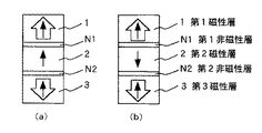
(第3の実施形態)
第2の実施形態とは逆に、第1の実施形態に示す層構成において第1磁性層1と第3磁性層3の保磁力を第2磁性層2の保磁力よりも低く設定すれば、図2に示すように、第2磁性層2の磁化方向を固定したまま、第1磁性層1及び第3磁性層3の磁化の方向を外部磁界によって変化させることができる。これにより、図2の(a)に示す低抵抗状態と(b)に示す高抵抗状態とを作ることができる。
【0020】
(第4の実施形態)
第2の実施形態の磁気抵抗素子において、第1磁性層1と第3磁性層3の磁化方向を一定にし、第2磁性層2の磁化方向を記録情報に応じて変化させ、読出し時に抵抗値を検出すれば、メモリ素子として機能させることができる。
【0021】
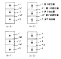
(第5の実施形態)
第2の実施形態に示す磁気抵抗素子において、第1磁性層1と第3磁性層3の磁化方向を記録情報に応じて変化させ、第2磁性層の磁化方向を読出し時に反転させることとすれば、メモリ素子とすることができる。図3にその例を示した。図3において、(a−1)及び(a−2)では、第1磁性層1及び第3磁性層3が上向きに記録されており、一方、(b−1)及び(b−2)では下向きに記録されており、それぞれが、“0”,“1”の二値のデータに相当する。(a−1)及び(a−2)の違いは、第2磁性層2の磁化の方向である。(b−1)及び(b−2)の違いも、第2磁性層2の磁化の方向である。各々の場合についてもいずれも、まず、素子に上向きの磁界を印加したのち、下向きの磁界を印加するものとする。この際の磁界は、第2磁性層2の磁化のみが反転するように、第2磁性層2の保磁力よりも大きく、第1磁性層1及び第3磁性層3の保磁力よりも小さく設定する。第1磁性層1及び第3磁性層3が上向きに記録されている場合は、抵抗値については、(a−1)が低い状態、(a−2)が高い状態であるため、高い状態から低い状態へ遷移するが、第1磁性層1及び第3磁性層3が下向きに記録されている場合は、抵抗値については、(b−1)が高い状態、(b−2)が低い状態であるため、低い状態から高い状態に遷移する。このような抵抗値の状態の変化をセンシングすれば、記録されている情報を読み出すことができる。
【0022】
(第6の実施形態)
第3の実施形態3の磁気抵抗素子において、第2磁性層2の磁化方向を一定にし、第1磁性層1と第3磁性層3の磁化方向を記録情報に応じて変化させ、読出し時に抵抗値を検出すれば、メモリ素子として機能させることができる。
【0023】
(第7の実施形態)
第3の実施形態の磁気抵抗素子において、第2磁性層2の磁化方向を記録情報に応じて変化させ、第1磁性層1及び第3磁性層3の磁化方向をいずれも読出し時に反転させることとすれば、この磁気抵抗素子をメモリ素子に応用することができる。図4にその例を示した。図4において、(a−1),(a−2)は第2磁性層2が上向きの状態を示し、これら両者の違いは、第1磁性層1及び第3磁性層3の磁化がいずれも上向きか下向きかである。また、(b−1),(b−2)では第2磁性層2が下向きに記録されており、両者は、第1磁性層1及び第3磁性層3の磁化がいずれも上向きか下向きかで相違している。(a−1),(a−2)は“0”,“1”の二値データの一方に対応し、(b−1),(b−2)は他方に対応する。
【0024】
この実施形態においても、第5の実施形態の場合と同様に、まず、素子に上向きの磁界を印加したのち、下向きの磁界を印加するものとする。この際の磁界は、第1磁性層1及び第3磁性層の磁化が反転し第2磁性層の磁化が反転しないように、第2磁性層2の保磁力よりも小さく、第1磁性層1及び第3磁性層3の保磁力よりも大きく設定する。そして、第5の実施形態と同様にして抵抗値の状態の変化をセンシングすれば、記録されている情報を読み出すことができる。
【0025】
(第8の実施形態)
第2の実施形態の磁気抵抗素子において、第1磁性層1の磁化の向きと第3磁性層3の磁化の向きを反平行にすることによって、第2磁性層2に印加される漏洩磁界を低減することができる。図5にこの素子構成を示した。図中、第1磁性層1及び第3磁性層3中の矢印のうち、外側の白抜きの矢印はその磁性層の総体としての磁化の向きを示しており、内側の黒実線の矢印は、磁気抵抗効果に影響を与える副格子磁化の向きを示している。
【0026】
第1磁性層1と第3磁性層3の磁化は反平行であるため、これらの磁性層の磁化から第2磁性層に印加される漏洩磁界は、相互に打ち消しあって弱まる。このため、第2磁性層2は、他の磁性層からの結合力を受けない単層膜のように振舞うことができ、反転磁界の増大やシフトなどをなくすことができる。
【0027】
(第9の実施形態)
第8の実施形態の磁気抵抗素子を実現するためには、第1磁性層1を鉄族元素副格子磁化優勢な希土類鉄族合金膜とし、第3磁性層を希土類元素副格子磁化優勢な希土類鉄族合金膜とすればよい。希土類鉄族合金膜は、希土類元素の副格子磁化と鉄族元素の副格子磁化が反平行であるフェリ磁性体であって、正味の磁化は、これらの副格子磁化の差となる。また、磁気抵抗に起因するのは、主に鉄族元素の副格子磁化である。よって、どちらかの磁性層を鉄族元素副格子磁化優勢、他の磁性層を希土類元素副格子磁化優勢とすれば、正味の磁化と磁気抵抗に起因する磁化の方向を反平行にしたりすることが可能である。
【0028】
また、第1磁性層1を希土類元素副格子磁化優勢、第3磁性層3を鉄族元素副格子磁化優勢としてもよい。
【0029】
(第10の実施形態)
本発明の磁気抵抗素子における各非磁性層N1,N2は、巨大磁気抵抗効果(GMR効果)がおきるようにCuなどの良導体にしてもよいし、スピントンネル効果がおきるようにAl2O3などの絶縁体にしてもよい。しかし、スピントンネル効果の方がGMR効果より磁気抵抗変化率が大きく、MRAMのメモリセルに適した抵抗値に設定することが可能なため、スピントンネル効果がおきるようにすることが好ましい。すなわち、第1非磁性層N1及び第2非磁性層N2の両方が絶縁層からなることが望ましい。
【0030】
(第11の実施形態)
本発明において、磁気抵抗素子を構成する垂直磁化膜である第1磁性層、第2磁性層及び第3磁性層は、膜面垂直方向に磁化しかつ磁気抵抗効果をもたらすものならどのようなものでも使用できる。そのような垂直磁化膜として、例えば、希土類鉄族合金膜、CoCr合金膜、ガーネット膜などを使用することができる。中でも、希土類−鉄族元素合金は、室温で成膜後に容易に垂直磁化膜となる点、アモルファス合金のため結晶粒界の悪影響がない点などから好ましい。したがって、第1磁性層1、第2磁性層2及び第3磁性層3の全てを希土類元素と鉄族元素との合金からなるフェリ磁性膜とすることが好ましい。
【0031】
希土類鉄族合金膜として、本発明における第1磁性層1、第2磁性層2及び第3磁性層3に使用できるものとして、例えば、GdFe,GdFeCo,TbFe,TbFeCo,DyFe,DyFeCoなどが挙げられる。これらの磁性膜は、垂直磁気異方性が、Gd,Dy,Tbを含む順に大きくなる傾向がある。このため、保磁力の高い層にはTbFe,TbFeCoなどを用いるのがよく、保磁力の低い層にはGdFeもしくはGdFeCoを用いるのがよい。
【0032】
また,第1磁性層、第2磁性層、第3磁性層の膜厚は、2nmから1μmまでの範囲が良い。これは,2nmより薄くなると磁化を一方向に保存しておくことが容易でなくなるためである。1μmより厚くなると加工が難しい、ラフネスが大きくなってトンネル障壁膜がショートする、などの製造プロセスの問題が発生するためであり、好ましくは100nm以下が良い。さらに望ましくは,5nm以上50nm以下がよい。
【0033】
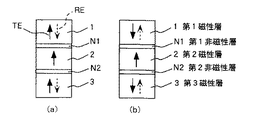
図6は、希土類元素と鉄族元素の合金からなるフェリ磁性膜を用いた本発明に基づく磁気抵抗素子の磁化状態を示したものである。層構成自体は第1の実施形態のものと同様である。第1磁性層1及び第3磁性層3における実線は鉄族元素(TE)の副格子磁化の向きを示し、点線は希土類元素(RE)の副格子磁化の向きを示している。図6は、第1磁性層1及び第3磁性層3の磁化の方向が一定であって第2磁性層2の磁化方向を反転させる場合を示している。
【0034】
交換結合力に関して鉄族元素の交換力が希土類元素の交換力よりも強いので、磁性層間の交換結合力には主に鉄族元素が寄与する。図6の(a)では鉄族元素副格子磁化が平行となっており、スピントンネル効果における低抵抗状態となっている。(b)では、第1磁性層1と第2磁性層2の間、及び、第2磁性層2と第3磁性層3の間では反平行磁化状態となっており、高抵抗状態となっている。
【0035】
また、図7は、図6に示すものと同じ原理であるが、第2磁性層2の磁化の方向が一定であって、第1磁性層1及び第3磁性層3の磁化が反転する場合を示している。
【0036】
この実施の形態においては、第1磁性層1、第2磁性層2及び第3磁性層3は、全て、希土類元素と鉄族元素との合金からなるフェリ磁性膜とするとことが好ましい。
【0037】
(第12の実施形態)
磁気抵抗効果、特にスピントンネル効果を高めて磁気抵抗変化率を高めるためには、非磁性層の両側に、スピン分極率の高い材料の磁性層を設けることが望ましい。第1磁性層、第2磁性層、第3磁性層は、膜面垂直方向に磁化した磁性膜である。これらの磁性膜が十分高い抵抗変化率を生じせしめない場合には、非磁性層の両側に抵抗変化率が高くなるような磁性膜を設けて、これらの磁性膜が垂直磁化膜と磁気的に結合するようにすればよい。抵抗変化率が高くなる磁性膜とは、特にスピントンネル効果の場合、スピン分極率が高いことに相当する。したがって、第1磁性層と第1非磁性層の間、第2磁性層と第1非磁性層の間、第2磁性層と第2非磁性層の間、第2非磁性層と第3磁性層の間の少なくとも1箇所に、スピン分極率の高い磁性層が設けると良い。
【0038】
また、磁気的な結合としては,交換結合と静磁結合が挙げられる。このうち、交換結合は、膜面に均一に作用し、磁性層間に非磁性層を設ける必要がないので、磁気的な結合としては、交換結合がより望ましい。
【0039】
スピン分極率が高い磁性層の膜厚としては、原子オーダーから、10nmの範囲がよい。好ましくは、1nmから5nmの範囲がよい。スピン分極率が高い材料は、フェロ磁性材料などがあげられ、例えばFe,Co,FeCoなどであり、磁化が大きいために反磁界により膜面内方向に磁化しやすい性質がある。第1磁性層、第2磁性層、第33磁性層と交換結合させて垂直方向に磁化させるためには薄いほうが、垂直に磁化させやすいからである。
【0040】
図8は、このようなスピン分極率の高い磁性層を有する磁気抵抗素子を示している。この磁気抵抗素子は、第1の実施形態の磁気抵抗素子において、第1磁性層1と第1非磁性層N1の間に高スピン分極率材料層M1、第1非磁性層N1と第2磁性層2の間に高スピン分極率材料層M2、第2磁性層2と第2非磁性層N2の間に高スピン分極率材料層M3、第2非磁性層N2と第3磁性層3の間に高スピン分極率材料層M4をそれぞれ設けた構成のものである。
【0041】
高スピン分極率材料層M1〜M4としては、Co,Fe,CoFeなどの層を用いることができるが、中でも、CoFeが、高いMR比を達成されるために、好ましい。またこれらの材料は、単独で膜形成した場合には面内磁化膜となるため、薄膜として形成して第1磁性層1、第2磁性層2、第3磁性層3などと交換結合させることにより垂直磁化膜とすることが好ましい。
【0042】
(第13の実施形態)
本発明に基づく前述した各実施形態の磁気抵抗素子に、垂直方向の磁界を発生させる磁場発生手段を設けることで、この磁場発生手段を用いて磁気抵抗素子に情報の記録を行い、メモリ素子とすることができる。例えば図9に示すように、図示しない絶縁膜を介して書き込み線900を磁気抵抗素子の近傍に配置する。ここで絶縁膜を設けるのは、磁気抵抗素子と書き込み線900との電気的な接触を防ぐためである。
【0043】
書き込み線900は、紙面の垂直方向に延びており、(a)では、紙面奥側に向かって電流を流すことにより、第2磁性層2の磁化を上向きとする。また(b)では、紙面から手前に向かって電流を流すことにより、第2磁性層1の磁化を下向きにすることができる。
【0044】
(第14の実施形態)
メモリ装置(MRAM)を構成する場合には、それぞれ上述したようなメモリ素子からなるメモリセルをマトリックス状に配置する。この際に生じるメモリセル間のクロストークを解消するためには、スイッチング素子を設けるとよい。
【0045】
図10は、スイッチング素子を有するメモリセルアレイを示したものであり、ここでは、メモリセルアレイ中の多数あるメモリセルのうちの1つのみを取り出して示したものである。実際には、図示横方向と奥手方向に同様のメモリセルが並んでおり、上面から見てマトリックス状に配置されている。
【0046】
図10において、シリコン半導体のp型基板33上に作成したn+領域であるソース領域32及びドレイン領域31と、ゲート電極80とからなるMOSFET(金属酸化物半導体電界効果トランジスタ)のうち、ドレイン領域31に上述の磁気抵抗素子の一端が接続されている。磁気抵抗素子の他端はセンス線40に接続される。
【0047】
記録情報の書き込み・消去は、紙面垂直方向に延びた書き込み線900と紙面横方向に延びたセンス線40とに電流を流すことで、それらの交点に位置した磁気抵抗素子(メモリセル)に記録を行うことができる。ソース領域32に接続された電極70は接地されており、センス線40の左端に電流源、右端にセンス回路を設けることで、磁気抵抗素子の抵抗値に応じた電位をセンス回路に与えることができ、情報の検出が可能となる。
【0048】
【発明の効果】
以上説明したように本発明は、磁気抵抗素子として垂直磁化膜を用いるとともに2つの非磁性層を設けることにより、素子を微細化しても安定に磁化情報を保存することができるとともに、MR比のバイアス依存性を改善することができるという効果がある。
【図面の簡単な説明】
【図1】本発明の第1の実施形態の磁気抵抗素子を示す断面図である。
【図2】第3の実施形態における磁気抵抗素子の磁化状態を示す図である。
【図3】第5の実施形態におけるメモリ素子からの情報の読出しを説明する図である。
【図4】第7の実施形態におけるメモリ素子からの情報の読出しを説明する図である。
【図5】第8の実施形態における磁気抵抗素子の磁化状態を説明する図である。
【図6】第11の実施形態における磁気抵抗素子の磁化状態の例を示す図である。
【図7】第11の実施形態における磁気抵抗素子の磁化状態の別の例を示す図である。
【図8】第12の実施形態の磁気抵抗素子の断面図である。
【図9】メモリ素子の基本構成を示す図である。
【図10】メモリセルの構成の一例を示す断面図である。
【図11】従来の磁気抵抗素子の構成の一例を示す断面図である。
【符号の説明】
1,11 第1磁性層
2,12 第2磁性層
3,13 第3磁性層
31 ドレイン領域
32 ソース領域
33 Si基板
40 センス線
70 ソース電極
80 ゲート電極
900 書き込み線
N1,N11 第1非磁性層
N2,N12 第2非磁性層
M1〜M4 高スピン分極率材料層[0001]
BACKGROUND OF THE INVENTION
The present invention relates to a magnetoresistive element used in a nonvolatile solid-state memory or the like, and in particular, a magnetoresistive element that is a double tunnel perpendicular magnetization TMR element, a memory element and a memory cell using the magnetoresistive element, and the like The present invention relates to a recording / reproducing method for a memory device.
[0002]
[Prior art]
In recent years, magnetic memories using magnetoresistive elements have been actively studied. A magnetic random access memory (MRAM) as a memory device using this magnetic memory element uses a magnetic film for storing information, so that information is not lost even when the power is turned off, that is, non-volatile. It has the characteristic of being.
[0003]
An MRAM memory cell is provided with a magnetoresistive element by a spin tunnel effect. This element is generally called a TMR element, and has a resistance change rate (MR ratio) larger than that of a conventional magnetoresistive element, and a resistance value of several KΩ to several tens KΩ, which is an optimum value as a memory cell of an MRAM. Therefore, it is generally used as a memory element of MRAM.
[0004]
However, this TMR element has a characteristic that the MR ratio decreases as the bias voltage applied to the element increases. For example, it has been reported that an MR ratio close to 50% is obtained at several mV, but about 20% at 500 mV. In the MRAM, since a bias voltage of several hundred mV is applied to the TMR element, this reduction rate is a level that cannot be ignored, and the detection sensitivity is deteriorated.
[0005]
As a countermeasure against the problem of the bias voltage dependency of the MR ratio of the TMR element, it has been proposed to use a TMR element provided with two insulating layers. For example, in Japanese Patent Laid-Open No. 9-260743, a tunnel junction film is formed by using a magnetic layer magnetized in the in-plane direction and a laminated structure of a magnetic layer, an insulating layer, a magnetic layer, an insulating layer, and a magnetic layer. An element is disclosed. FIG. 11 shows the structure of a conventional TMR element having two insulating layers, where (a) shows the magnetization state corresponding to one of the binary recordings, and (b) shows the other of the binary recordings. The corresponding magnetization state is shown. In the figure, arrows indicate the magnetization directions of the magnetic layers. The TMR element includes a first
[0006]
In such a TMR element provided with two insulating layers, the bias voltage applied to one tunnel barrier film is halved in the same way as two normal TMR elements are connected in series. There is an effect that deterioration due to is reduced.
[0007]
[Problems to be solved by the invention]
However, although the conventional magnetoresistive element shown in FIG. 11 has an effect on the bias voltage dependence, there arises a problem that the magnetization state becomes unstable when the element size is reduced. This occurs because the in-plane magnetization film is used for the magnetoresistive element. In particular, in the case of the magnetization state shown in FIG. 11A, the magnetization of each magnetic layer is directed in the same direction. A self-magnetic field (demagnetizing field) is applied to each layer by the magnetic poles on the end face of each, and the magnetization state of each layer becomes more unstable. For this reason, in order to achieve magnetization orientation in one direction as in the state shown in (a), it is common to take measures by improving the element shape such as lengthening the magnetic film in the direction of the easy axis of magnetization. This increases the element size and increases the memory cell area, that is, decreases the degree of integration.
[0008]
Further, of the two states (a) and (b) in FIG. 11, the state (b) is an energetically stable state because the magnetic flux emitted from the
[0009]
These problems of instability and switching magnetic field tend to become more prominent when the element size is reduced. Therefore, in the conventionally proposed element, there is a problem that when the degree of integration is increased, the magnetization state becomes unstable or the switching magnetic field increases.
[0010]
Therefore, an object of the present invention is to provide a magnetoresistive element that can stably perform recording of information with a low current consumption while maintaining a stable magnetization state, a memory element and a memory cell using such a magnetoresistive element, It is an object of the present invention to provide a recording / reproducing method for these memory elements.
[0011]
[Means for Solving the Problems]
In view of the above-described problems, the present inventor uses a magnetic film having a small demagnetizing field energy as a magnetic film constituting the magnetoresistive element, and further, there is a difference in energy between the antiparallel magnetization state and the parallel magnetization state. The inventors have found that the above problems can be solved by using a small number of medium configurations, and have completed the present invention.
[0012]
In other words, the above purpose is
(1) The first magnetic layer magnetized in the direction perpendicular to the film surface, the first nonmagnetic layer, the second magnetic layer magnetized in the direction perpendicular to the film surface, the second nonmagnetic layer, and magnetized in the direction perpendicular to the film surface The third magnetic layerThe coercive force of each of the first magnetic layer and the third magnetic layer is smaller than that of the second magnetic layer.Magnetoresistive elementA method of recording / reproducing a memory device having a magnetic element, wherein the magnetization direction of the second magnetic layer is changed according to the recording information, and the magnetization directions of the first magnetic layer and the third magnetic layer are reversed during reading. Recording / reproducing method for memory device,as well as,
(2) The magnetization direction of the first magnetic layer and the magnetization direction of the third magnetic layer are antiparallel (1)Recording / reproducing method of memory element,as well as,
(3) One of the first magnetic layer and the third magnetic layer is an iron group element sublattice magnetization dominant rare earth iron group alloy film, and the other of the first magnetic layer and the third magnetic layer is a rare earth element sublattice magnetization dominant rare earth iron Group alloy film, (2)Recording / reproducing method of memory element,as well as,
(4) The first nonmagnetic layer and the second nonmagnetic layer are made of an insulating layer.3)Recording / reproducing method of memory element,as well as,
(5)A method of recording and reproducing a memory element according to any one of (1) to (4), wherein a plurality of memory elements are arranged on a substrate, and at least one of the memory elements is selected to record and reproduce information. as well as,
(6)The first magnetic layer magnetized in the direction perpendicular to the film surface, the first nonmagnetic layer, the second magnetic layer magnetized in the direction perpendicular to the film surface, the second nonmagnetic layer, and the third magnetic material magnetized in the direction perpendicular to the film surface Are stacked in order, between the first magnetic layer and the first nonmagnetic layer, between the second magnetic layer and the first nonmagnetic layer, between the second magnetic layer and the second nonmagnetic layer, and second nonmagnetic. A magnetic layer having a higher spin polarizability than that of the first magnetic layer, the second magnetic layer, or the third magnetic layer is provided in at least one of the layers and the third magnetic layer. A magnetoresistive element comprising CoFe, and
(7)The magnetoresistive element according to (6), a magnetic field generating means for generating a magnetic field perpendicular to the film surface of the magnetoresistive element, and the magnetoresistive element are provided on the substrate, and one end thereof is used as a drain region of the field effect transistor Magnetic random access memory having memory cells connected and connected at the other end to a bit line,
Achieved by:
[0013]
DETAILED DESCRIPTION OF THE INVENTION
Next, a preferred embodiment of the present invention will be described with reference to the drawings.
[0014]
(First embodiment)
FIG. 1 shows an example of the structure of the magnetoresistive element according to the first embodiment of the present invention. The arrows in the figure indicate the magnetization directions of the magnetic layers, and (a) and (b) indicate the two magnetization states that can be stably taken by the magnetoresistive element.
[0015]
The magnetoresistive element includes a first
[0016]
Thus, in a TMR element including two insulating layers, a voltage that is ½ of the voltage applied to the top and bottom of the element is applied to each insulating layer. For this reason, the dependency of the MR ratio on the bias voltage is reduced, and the deterioration of the MR ratio can be suppressed.
[0017]
In addition, the perpendicular magnetization film generally has a small demagnetizing field energy and the magnitude of magnetization is smaller than that of the in-plane magnetization film. Therefore, according to this magnetoresistive element, the magnitude of the magnetic field applied to the other magnetic layer from the magnetization of each laminated magnetic layer can be reduced, and the antiparallel magnetization state can be easily obtained. Further, since the magnetic field applied to the other magnetic layer can be reduced when there is no external magnetic field, the shift amount by which the MR curve (a graph showing the relationship between the resistance and the applied magnetic field) is shifted by the leakage magnetic field is reduced. The fact that this shift magnetic field (offset magnetic field) can be reduced means that an increase in the reversal magnetic field can be suppressed, and thus power consumption can be suppressed.
[0018]
(Second Embodiment)
The magnetization state in which only the magnetization direction of the second
[0019]
(Third embodiment)
Contrary to the second embodiment, if the coercivity of the first
[0020]
(Fourth embodiment)
In the magnetoresistive element of the second embodiment, the magnetization directions of the first
[0021]
(Fifth embodiment)
In the magnetoresistive element shown in the second embodiment, the magnetization directions of the first
[0022]
(Sixth embodiment)
In the magnetoresistive element according to the third embodiment, the magnetization direction of the second
[0023]
(Seventh embodiment)
In the magnetoresistive element of the third embodiment, the magnetization direction of the second
[0024]
Also in this embodiment, as in the case of the fifth embodiment, first, an upward magnetic field is applied to the element, and then a downward magnetic field is applied. The magnetic field at this time is smaller than the coercive force of the second
[0025]
(Eighth embodiment)
In the magnetoresistive element of the second embodiment, the leakage magnetic field applied to the second
[0026]
Since the magnetizations of the first
[0027]
(Ninth embodiment)
In order to realize the magnetoresistive element of the eighth embodiment, the first
[0028]
Alternatively, the first
[0029]
(Tenth embodiment)
Each nonmagnetic layer N1, N2 in the magnetoresistive element of the present invention may be a good conductor such as Cu so that a giant magnetoresistive effect (GMR effect) occurs, or Al so that a spin tunnel effect can occur.2OThreeIt may be an insulator. However, the spin tunnel effect has a larger magnetoresistance change rate than the GMR effect and can be set to a resistance value suitable for the memory cell of the MRAM. Therefore, it is preferable that the spin tunnel effect occurs. That is, it is desirable that both the first nonmagnetic layer N1 and the second nonmagnetic layer N2 are made of insulating layers.
[0030]
(Eleventh embodiment)
In the present invention, the first magnetic layer, the second magnetic layer, and the third magnetic layer, which are perpendicular magnetic films constituting the magnetoresistive element, are any materials that are magnetized in the direction perpendicular to the film surface and provide a magnetoresistive effect. But you can use it. As such a perpendicular magnetization film, for example, a rare earth iron group alloy film, a CoCr alloy film, a garnet film or the like can be used. Among these, a rare earth-iron group element alloy is preferable because it easily becomes a perpendicular magnetization film after film formation at room temperature, and because it is an amorphous alloy, there is no adverse effect of crystal grain boundaries. Therefore, it is preferable that all of the first
[0031]
Examples of rare earth iron group alloy films that can be used for the first
[0032]
The film thickness of the first magnetic layer, the second magnetic layer, and the third magnetic layer is preferably in the range of 2 nm to 1 μm. This is because it is not easy to store the magnetization in one direction when the thickness is thinner than 2 nm. If the thickness is larger than 1 μm, processing is difficult, and the roughness becomes so large that the tunnel barrier film is short-circuited. Problems with manufacturing processes such as 100 nm or less are preferable. More preferably, it is 5 nm or more and 50 nm or less.
[0033]
FIG. 6 shows the magnetization state of a magnetoresistive element according to the present invention using a ferrimagnetic film made of an alloy of a rare earth element and an iron group element. The layer structure itself is the same as that of the first embodiment. The solid lines in the first
[0034]
Since the exchange force of the iron group element is stronger than the exchange force of the rare earth element with respect to the exchange coupling force, the iron group element mainly contributes to the exchange coupling force between the magnetic layers. In FIG. 6A, the iron group element sublattice magnetizations are parallel to each other, which is a low resistance state in the spin tunnel effect. In (b), between the 1st
[0035]
FIG. 7 shows the same principle as that shown in FIG. 6, but the magnetization direction of the second
[0036]
In this embodiment, the first
[0037]
(Twelfth embodiment)
In order to increase the magnetoresistance effect, particularly the spin tunneling effect and increase the magnetoresistance change rate, it is desirable to provide a magnetic layer made of a material having a high spin polarizability on both sides of the nonmagnetic layer. The first magnetic layer, the second magnetic layer, and the third magnetic layer are magnetic films magnetized in the direction perpendicular to the film surface. If these magnetic films do not cause a sufficiently high resistance change rate, magnetic films that increase the resistance change rate are provided on both sides of the nonmagnetic layer, and these magnetic films are magnetically coupled to the perpendicular magnetization film. What is necessary is just to make it couple | bond. The magnetic film having a high resistance change rate corresponds to a high spin polarizability, particularly in the case of the spin tunnel effect. Therefore, between the first magnetic layer and the first nonmagnetic layer, between the second magnetic layer and the first nonmagnetic layer, between the second magnetic layer and the second nonmagnetic layer, and between the second nonmagnetic layer and the third magnetic layer. A magnetic layer having a high spin polarizability is preferably provided at least at one position between the layers.
[0038]
Examples of the magnetic coupling include exchange coupling and magnetostatic coupling. Among these, exchange coupling acts uniformly on the film surface, and it is not necessary to provide a nonmagnetic layer between the magnetic layers, so exchange coupling is more desirable as the magnetic coupling.
[0039]
The film thickness of the magnetic layer having a high spin polarizability is preferably in the range of 10 nm from the atomic order. A range of 1 nm to 5 nm is preferable. Examples of the material having a high spin polarizability include ferromagnetic materials such as Fe, Co, FeCo, and the like. Since the magnetization is large, the material has a property of being easily magnetized in the in-plane direction by a demagnetizing field. This is because in order to exchange-couple with the first magnetic layer, the second magnetic layer, and the 33rd magnetic layer and magnetize in the vertical direction, the thinner one is easier to magnetize.
[0040]
FIG. 8 shows a magnetoresistive element having such a magnetic layer with a high spin polarizability. This magnetoresistive element is the same as the magnetoresistive element of the first embodiment, except that the high spin polarizability material layer M1, the first nonmagnetic layer N1, and the second magnetic layer are provided between the first
[0041]
As the high spin polarizability material layers M <b> 1 to M <b> 4, layers such as Co, Fe, and CoFe can be used. Among them, CoFe is preferable because a high MR ratio is achieved. In addition, since these materials become in-plane magnetization films when formed alone, they are formed as thin films and exchange-coupled with the first
[0042]
(13th Embodiment)
By providing magnetic field generating means for generating a magnetic field in the vertical direction in the magnetoresistive element of each of the above-described embodiments based on the present invention, information is recorded on the magnetoresistive element using this magnetic field generating means, and the memory element and can do. For example, as shown in FIG. 9, the
[0043]
The
[0044]
(Fourteenth embodiment)
When configuring a memory device (MRAM), memory cells each having the above-described memory elements are arranged in a matrix. In order to eliminate crosstalk between memory cells generated at this time, a switching element may be provided.
[0045]
FIG. 10 shows a memory cell array having switching elements. Here, only one of a large number of memory cells in the memory cell array is extracted and shown. Actually, similar memory cells are arranged in the horizontal direction and the back direction in the figure, and are arranged in a matrix as viewed from above.
[0046]
In FIG. 10, n formed on a p-
[0047]
Recording / writing of recorded information is performed by recording a current in a magnetoresistive element (memory cell) located at the intersection of a
[0048]
【The invention's effect】
As described above, according to the present invention, by using a perpendicular magnetization film as a magnetoresistive element and providing two nonmagnetic layers, it is possible to stably store magnetization information even if the element is miniaturized, and the MR ratio. There is an effect that the bias dependency can be improved.
[Brief description of the drawings]
FIG. 1 is a cross-sectional view showing a magnetoresistive element according to a first embodiment of the present invention.
FIG. 2 is a diagram showing a magnetization state of a magnetoresistive element in a third embodiment.
FIG. 3 is a diagram for explaining reading of information from a memory element according to a fifth embodiment.
FIG. 4 is a diagram for explaining reading of information from a memory element in a seventh embodiment.
FIG. 5 is a diagram for explaining a magnetization state of a magnetoresistive element in an eighth embodiment.
FIG. 6 is a diagram showing an example of a magnetization state of a magnetoresistive element in an eleventh embodiment.
FIG. 7 is a diagram showing another example of the magnetization state of the magnetoresistive element in the eleventh embodiment.
FIG. 8 is a cross-sectional view of a magnetoresistive element according to a twelfth embodiment.
FIG. 9 is a diagram showing a basic configuration of a memory element.
FIG. 10 is a cross-sectional view illustrating an example of a structure of a memory cell.
FIG. 11 is a cross-sectional view showing an example of the configuration of a conventional magnetoresistive element.
[Explanation of symbols]
1,11 First magnetic layer
2,12 Second magnetic layer
3,13 Third magnetic layer
31 Drain region
32 source regions
33 Si substrate
40 sense lines
70 Source electrode
80 Gate electrode
900 Write line
N1, N11 first nonmagnetic layer
N2, N12 second nonmagnetic layer
M1-M4 high spin polarizability material layer
Claims (7)
前記第2磁性層の磁化方向を記録情報に応じて変化させ、前記第1磁性層及び前記第3磁性層の磁化方向を読出し時に反転させるようにしたことを特徴とするメモリ素子の記録再生方法。The first magnetic layer magnetized in the direction perpendicular to the film surface, the first nonmagnetic layer, the second magnetic layer magnetized in the direction perpendicular to the film surface, the second nonmagnetic layer, and the third magnetic material magnetized in the direction perpendicular to the film surface A memory element having a magnetoresistive element in which a coercive force of each of the first magnetic layer and the third magnetic layer is smaller than a coercive force of the second magnetic layer ,
A recording / reproducing method for a memory element, wherein the magnetization direction of the second magnetic layer is changed according to recording information, and the magnetization directions of the first magnetic layer and the third magnetic layer are reversed at the time of reading. .
前記磁気抵抗素子の膜面に垂直方向の磁界を発生する磁場発生手段と、Magnetic field generating means for generating a magnetic field perpendicular to the film surface of the magnetoresistive element;
前記磁気抵抗素子を含み、その一端を電界効果トランジスタのドレイン領域に接続し、他端をビット線に接続したメモリセルを有することを特徴とする磁気ランダムアクセスメモリ。A magnetic random access memory comprising a memory cell including the magnetoresistive element, having one end connected to a drain region of a field effect transistor and the other end connected to a bit line.
Priority Applications (7)
| Application Number | Priority Date | Filing Date | Title |
|---|---|---|---|
| JP2001078470A JP3658331B2 (en) | 2001-03-19 | 2001-03-19 | Recording / reproducing method of memory element, magnetoresistive element, and magnetic random access memory |
| US10/098,116 US6713830B2 (en) | 2001-03-19 | 2002-03-15 | Magnetoresistive element, memory element using the magnetoresistive element, and recording/reproduction method for the memory element |
| TW091105059A TWI272610B (en) | 2001-03-19 | 2002-03-18 | Magnetoresistive element, memory element using the magnetoresistive element, and recording/reproduction method for the memory element |
| DE60216838T DE60216838T2 (en) | 2001-03-19 | 2002-03-18 | Magnetoresistive element, memory element with this magnetoresistive element, and recording / reproducing method for the memory element |
| EP02006094A EP1244117B1 (en) | 2001-03-19 | 2002-03-18 | Magnetoresistive element, memory element using the magnetorestistive element, and recording/reproduction method for the memory element |
| CNB021206007A CN100490003C (en) | 2001-03-19 | 2002-03-19 | Magnetic resistance element, storage element using same and relative recording/reproducing method |
| KR10-2002-0014631A KR100502113B1 (en) | 2001-03-19 | 2002-03-19 | Magnetoresistive element, memory element using the magnetoresistive element, and recording/reproduction method for the memory element |
Applications Claiming Priority (1)
| Application Number | Priority Date | Filing Date | Title |
|---|---|---|---|
| JP2001078470A JP3658331B2 (en) | 2001-03-19 | 2001-03-19 | Recording / reproducing method of memory element, magnetoresistive element, and magnetic random access memory |
Publications (2)
| Publication Number | Publication Date |
|---|---|
| JP2002280638A JP2002280638A (en) | 2002-09-27 |
| JP3658331B2 true JP3658331B2 (en) | 2005-06-08 |
Family
ID=18935081
Family Applications (1)
| Application Number | Title | Priority Date | Filing Date |
|---|---|---|---|
| JP2001078470A Expired - Lifetime JP3658331B2 (en) | 2001-03-19 | 2001-03-19 | Recording / reproducing method of memory element, magnetoresistive element, and magnetic random access memory |
Country Status (1)
| Country | Link |
|---|---|
| JP (1) | JP3658331B2 (en) |
Families Citing this family (4)
| Publication number | Priority date | Publication date | Assignee | Title |
|---|---|---|---|---|
| JP4444241B2 (en) | 2005-10-19 | 2010-03-31 | 株式会社東芝 | Magnetoresistive element, magnetic random access memory, electronic card and electronic device |
| JP2008283207A (en) * | 2005-10-19 | 2008-11-20 | Toshiba Corp | Magnetoresistive element, magnetic random access memory, electronic card and electronic device |
| US20090218645A1 (en) * | 2007-02-12 | 2009-09-03 | Yadav Technology Inc. | multi-state spin-torque transfer magnetic random access memory |
| JP4875037B2 (en) * | 2008-09-24 | 2012-02-15 | 株式会社東芝 | Magnetic memory, reproducing method thereof, and writing method |
-
2001
- 2001-03-19 JP JP2001078470A patent/JP3658331B2/en not_active Expired - Lifetime
Also Published As
| Publication number | Publication date |
|---|---|
| JP2002280638A (en) | 2002-09-27 |
Similar Documents
| Publication | Publication Date | Title |
|---|---|---|
| EP0875901B1 (en) | Magnetic thin-film memory element utilizing GMR effect, and magnetic thin-film memory | |
| JP3679593B2 (en) | Magnetic thin film element, magnetic thin film memory element and recording / reproducing method thereof | |
| JP3667244B2 (en) | Magnetoresistive element, memory element using the same, magnetic random access memory, and method for recording / reproducing magnetic random access memory | |
| US6713830B2 (en) | Magnetoresistive element, memory element using the magnetoresistive element, and recording/reproduction method for the memory element | |
| US7018725B2 (en) | Magneto-resistance effect element magneto-resistance effect memory cell, MRAM, and method for performing information write to or read from the magneto-resistance effect memory cell | |
| US6628542B2 (en) | Magnetoresistive device and magnetic memory using the same | |
| US6104632A (en) | Magnetic thin film memory and recording and reproducing method and apparatus using such a memory | |
| JP4896341B2 (en) | Magnetic random access memory and operating method thereof | |
| JP3634761B2 (en) | Magnetoresistive element, memory element using the magnetoresistive element, magnetic random access memory, and recording / reproducing method | |
| JP2000187976A (en) | Magnetic thin film memory and recording / reproducing method thereof | |
| US20020044479A1 (en) | Magnetoresistive element, and magnetic memory using the same | |
| JP3848119B2 (en) | Nonvolatile solid-state memory using magnetoresistance effect | |
| JP3891511B2 (en) | Magnetic thin film memory and recording / reproducing method thereof | |
| JP3658331B2 (en) | Recording / reproducing method of memory element, magnetoresistive element, and magnetic random access memory | |
| JP2003142753A (en) | Method for reversing magnetization of magnetic film, magnetoresistive film and magnetic memory using the same | |
| JP4136028B2 (en) | Magnetic thin film memory element, magnetic thin film memory using the same, and recording / reproducing method thereof | |
| JP2005203535A (en) | Magnetic memory | |
| JP2001256773A (en) | Method of accessing magnetic memory cell and magnetic memory cell | |
| JPH113584A (en) | Magnetic thin film memory element, method of manufacturing the same, and recording / reproducing method | |
| JP2003077269A (en) | Non-volatile solid-state memory element and memory using magnetoresistance effect and recording / reproducing method thereof | |
| JPH10302457A (en) | Magnetic thin film memory element and magnetic thin film memory using the same | |
| JP2003110165A (en) | Magnetoresistance effect element, ferromagnetic memory and information device |
Legal Events
| Date | Code | Title | Description |
|---|---|---|---|
| A131 | Notification of reasons for refusal |
Free format text: JAPANESE INTERMEDIATE CODE: A131 Effective date: 20041208 |
|
| A521 | Request for written amendment filed |
Free format text: JAPANESE INTERMEDIATE CODE: A523 Effective date: 20050207 |
|
| RD03 | Notification of appointment of power of attorney |
Free format text: JAPANESE INTERMEDIATE CODE: A7423 Effective date: 20050207 |
|
| TRDD | Decision of grant or rejection written | ||
| A01 | Written decision to grant a patent or to grant a registration (utility model) |
Free format text: JAPANESE INTERMEDIATE CODE: A01 Effective date: 20050302 |
|
| A61 | First payment of annual fees (during grant procedure) |
Free format text: JAPANESE INTERMEDIATE CODE: A61 Effective date: 20050311 |
|
| R150 | Certificate of patent or registration of utility model |
Free format text: JAPANESE INTERMEDIATE CODE: R150 Ref document number: 3658331 Country of ref document: JP Free format text: JAPANESE INTERMEDIATE CODE: R150 |
|
| FPAY | Renewal fee payment (event date is renewal date of database) |
Free format text: PAYMENT UNTIL: 20080318 Year of fee payment: 3 |
|
| FPAY | Renewal fee payment (event date is renewal date of database) |
Free format text: PAYMENT UNTIL: 20090318 Year of fee payment: 4 |
|
| FPAY | Renewal fee payment (event date is renewal date of database) |
Free format text: PAYMENT UNTIL: 20100318 Year of fee payment: 5 |
|
| FPAY | Renewal fee payment (event date is renewal date of database) |
Free format text: PAYMENT UNTIL: 20100318 Year of fee payment: 5 |
|
| FPAY | Renewal fee payment (event date is renewal date of database) |
Free format text: PAYMENT UNTIL: 20110318 Year of fee payment: 6 |
|
| FPAY | Renewal fee payment (event date is renewal date of database) |
Free format text: PAYMENT UNTIL: 20120318 Year of fee payment: 7 |
|
| FPAY | Renewal fee payment (event date is renewal date of database) |
Free format text: PAYMENT UNTIL: 20130318 Year of fee payment: 8 |
|
| FPAY | Renewal fee payment (event date is renewal date of database) |
Free format text: PAYMENT UNTIL: 20140318 Year of fee payment: 9 |
|
| EXPY | Cancellation because of completion of term |