JP3649867B2 - Manufacturing method of semiconductor devices - Google Patents
Manufacturing method of semiconductor devices Download PDFInfo
- Publication number
- JP3649867B2 JP3649867B2 JP22470097A JP22470097A JP3649867B2 JP 3649867 B2 JP3649867 B2 JP 3649867B2 JP 22470097 A JP22470097 A JP 22470097A JP 22470097 A JP22470097 A JP 22470097A JP 3649867 B2 JP3649867 B2 JP 3649867B2
- Authority
- JP
- Japan
- Prior art keywords
- platter
- substrate
- temperature
- semiconductor layer
- radiation thermometer
- Prior art date
- Legal status (The legal status is an assumption and is not a legal conclusion. Google has not performed a legal analysis and makes no representation as to the accuracy of the status listed.)
- Expired - Fee Related
Links
- 239000004065 semiconductor Substances 0.000 title claims description 66
- 238000004519 manufacturing process Methods 0.000 title claims description 13
- 239000000758 substrate Substances 0.000 claims description 86
- 230000005855 radiation Effects 0.000 claims description 47
- 229910002601 GaN Inorganic materials 0.000 claims description 23
- 229910052594 sapphire Inorganic materials 0.000 claims description 19
- 239000010980 sapphire Substances 0.000 claims description 19
- -1 gallium nitride compound Chemical class 0.000 claims description 17
- 239000012495 reaction gas Substances 0.000 claims description 9
- 238000000034 method Methods 0.000 claims description 8
- 239000000463 material Substances 0.000 claims description 4
- 238000009529 body temperature measurement Methods 0.000 description 12
- 150000001875 compounds Chemical class 0.000 description 6
- 239000007789 gas Substances 0.000 description 6
- 239000006227 byproduct Substances 0.000 description 4
- 238000005259 measurement Methods 0.000 description 4
- JMASRVWKEDWRBT-UHFFFAOYSA-N Gallium nitride Chemical compound [Ga]#N JMASRVWKEDWRBT-UHFFFAOYSA-N 0.000 description 3
- 239000002019 doping agent Substances 0.000 description 3
- 230000000694 effects Effects 0.000 description 3
- 229910021478 group 5 element Inorganic materials 0.000 description 3
- 239000000523 sample Substances 0.000 description 3
- JLTRXTDYQLMHGR-UHFFFAOYSA-N trimethylaluminium Chemical compound C[Al](C)C JLTRXTDYQLMHGR-UHFFFAOYSA-N 0.000 description 3
- IBEFSUTVZWZJEL-UHFFFAOYSA-N trimethylindium Chemical compound C[In](C)C IBEFSUTVZWZJEL-UHFFFAOYSA-N 0.000 description 3
- XUIMIQQOPSSXEZ-UHFFFAOYSA-N Silicon Chemical compound [Si] XUIMIQQOPSSXEZ-UHFFFAOYSA-N 0.000 description 2
- 229910052782 aluminium Inorganic materials 0.000 description 2
- 238000010586 diagram Methods 0.000 description 2
- 229910052733 gallium Inorganic materials 0.000 description 2
- 239000011521 glass Substances 0.000 description 2
- 229910052738 indium Inorganic materials 0.000 description 2
- 238000012423 maintenance Methods 0.000 description 2
- 229910052751 metal Inorganic materials 0.000 description 2
- 239000002184 metal Substances 0.000 description 2
- 238000012544 monitoring process Methods 0.000 description 2
- 238000012545 processing Methods 0.000 description 2
- 239000010453 quartz Substances 0.000 description 2
- 229910052710 silicon Inorganic materials 0.000 description 2
- 239000010703 silicon Substances 0.000 description 2
- VYPSYNLAJGMNEJ-UHFFFAOYSA-N silicon dioxide Inorganic materials O=[Si]=O VYPSYNLAJGMNEJ-UHFFFAOYSA-N 0.000 description 2
- XCZXGTMEAKBVPV-UHFFFAOYSA-N trimethylgallium Chemical compound C[Ga](C)C XCZXGTMEAKBVPV-UHFFFAOYSA-N 0.000 description 2
- 229910002704 AlGaN Inorganic materials 0.000 description 1
- MHYQBXJRURFKIN-UHFFFAOYSA-N C1(C=CC=C1)[Mg] Chemical compound C1(C=CC=C1)[Mg] MHYQBXJRURFKIN-UHFFFAOYSA-N 0.000 description 1
- 239000000956 alloy Substances 0.000 description 1
- 229910045601 alloy Inorganic materials 0.000 description 1
- 238000000137 annealing Methods 0.000 description 1
- 229910052785 arsenic Inorganic materials 0.000 description 1
- 239000000969 carrier Substances 0.000 description 1
- 238000005229 chemical vapour deposition Methods 0.000 description 1
- 238000005253 cladding Methods 0.000 description 1
- 238000011109 contamination Methods 0.000 description 1
- 239000013078 crystal Substances 0.000 description 1
- 238000009792 diffusion process Methods 0.000 description 1
- 238000005530 etching Methods 0.000 description 1
- 229910052737 gold Inorganic materials 0.000 description 1
- 238000010438 heat treatment Methods 0.000 description 1
- 239000003779 heat-resistant material Substances 0.000 description 1
- 238000011065 in-situ storage Methods 0.000 description 1
- 238000010030 laminating Methods 0.000 description 1
- 239000000203 mixture Substances 0.000 description 1
- 229910052750 molybdenum Inorganic materials 0.000 description 1
- 229910052759 nickel Inorganic materials 0.000 description 1
- 230000003287 optical effect Effects 0.000 description 1
- 238000002360 preparation method Methods 0.000 description 1
- 230000003746 surface roughness Effects 0.000 description 1
Images


Landscapes
- Testing Or Measuring Of Semiconductors Or The Like (AREA)
- Recrystallisation Techniques (AREA)
Description
【0001】
【発明の属する技術分野】
本発明は、たとえばMOCVD(有機金属化学気相成長)法により基板上に半導体層をエピタキシャル成長する場合に、基板の温度を正確に制御しながらエピタキシャル成長をすることができる半導体装置の製法に関する。さらに詳しくは、半導体層の積層によっても測定温度の誤差が生じないように温度を測定しながらエピタキシャル成長をすることができ、さらにバッチ処理を重ねていっても再現性よく温度制御ができる半導体装置の製法に関する。
【0002】
【従来の技術】
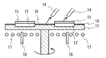
従来、たとえばMOCVD法などによりウェハ状の基板に半導体層をエピタキシャル成長する場合、図3に示されるように、反応装置内のウェハ状の基板を載置するプラッター11の凹部にウェハ状の基板12を載置する。そして、図示しないモータなどによりプラッター11を回転させながら、プラッター11の下からヒータ17により加熱するとともに、プラッター11の下でヒータ17に接しないように、熱電対温度計18、もしくはプラッター11の上方からの放射温度計(赤外線温度計)14などにより、温度を測定しながら所定の温度に制御する。前記熱電対温度計18の場合、プラッター11の下面とヒータ17からの熱伝導と熱輻射を受け、前記放射温度計14の場合、基板12からの熱輻射により、また、基板12が載置されない部分のプラッター11の表面からの熱輻射により温度を測定する。この測定値に基づいて所定の温度に制御する。そして反応ガスを装置内に導入し、反応させることにより基板12上に半導体層をエピタキシャル成長する。
【0003】
これらの方法で、たとえばサファイア基板12上にチッ化ガリウム系化合物半導体を積層する場合、前述の放射温度計14で温度を制御する場合、サファイア基板12、チッ化ガリウム系化合物半導体層15はともに熱輻射に対して透明であるので、放射温度計14によって、その基板12の下のプラッター11の表面からの熱輻射により温度を測定することができる。一方、基板12が載置されない部分は、チッ化ガリウム系化合物半導体層がエピタキシャル成長せず、熱輻射に対して不透明な反応副生成物による堆積物層16がプラッター11の表面を覆う。そのため、堆積物層16の表面からの熱輻射により温度を測定することになる。
【0004】
【発明が解決しようとする課題】
前述の熱電対温度計18で温度を制御する場合、熱電対温度計18のプローブとプラッター11とヒータ17の位置関係が正確な温度測定に非常に重要である。これらの構成部品の位置関係が少しでも狂うと、温度測定値がずれる。このような理由により、半導体成長装置のメンテナンスにおいて、これら構成部品の組立て時、これらの位置関係には細心の注意を払わなければならない。かなり注意深く組み立てても、メンテナンス前後で温度測定値がずれていることが多々ある。また、半導体成長装置を使い込んでゆくと、熱により、ヒータ17がたわみ、位置関係がずれる。これも温度測定値のずれの原因となる。さらに、半導体成長装置を使い込んでゆくと、熱電対温度計18のプローブ部分に反応副生成物が堆積する。これにより、反応副生成物を含めたプローブ全体の熱容量が変化し、温度測定値がずれる。熱電対温度計18による温度制御での問題は上述のように、バッチごとで温度測定値の再現性をとるのが難しいという点である。
【0005】
一方、前述の放射温度計14で温度を制御する場合、図4に示されるようにサファイア基板12とチッ化ガリウム系化合物半導体層15との境界面や、チッ化ガリウム系化合物半導体層15表面で熱輻射(波長が赤外領域の電磁波)が反射する。T0 、T1 、T2 …をそれぞれ0、1、2回サファイア基板12とチッ化ガリウム系化合物半導体層15の界面で反射した熱輻射とすると、放射温度計が受ける全熱輻射Tは数1で表される。
【0006】
【数1】
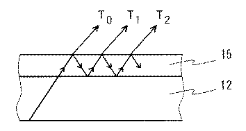
チッ化ガリウム系化合物半導体層の膜厚増加により、Tn とTm (n≠m)の光路差が熱輻射の波長の整数倍になったとき、Tn とTm は干渉し、Tは大きくなり、半整数倍になったとき弱くなる。つまり、チッ化ガリウム系化合物半導体層15の成長と共に測定する温度の値が振動して正確な温度測定をすることができないという問題がある。この問題は、たとえばジャパニーズ ジャーナル オブ アプライド フィジックス(Jpn.J.Appl.Phys.)第30巻、第8号(1991年、8月)の1620〜1627頁「干渉効果を用いたチッ化ガリウム成長のその場観察(In Situ Monitoring of GaN Growth Using Interference Effects )」にも記載されている。
【0008】
実際のプラッター11の温度は一定にもかかわらず、温度測定値は熱輻射の干渉によって振動する。半導体装置の温度制御部は、この測定値の振動に対応して、この振動を打ち消すようにヒータ17へ電流を供給する。その結果、プラッター11の温度は測定値とは逆位相で振動する事となり、均一なエピタキシャル成長は望めない。
【0009】
また、基板のない部分でのプラッターの表面の熱輻射により温度測定をする場合は、その上に積層される凹凸の堆積物層からの熱輻射により測定することになり、反応副生成物とプラッターのCなどの材料とで放射率(輻射率)が異なるため、反応副生成物が堆積するにつれ、測定温度がずれてくる。その結果、前述のいずれの方法においても、プラッター上の正確な温度を測定することができず、均一なエピタキシャル成長をすることができないという問題がある。
【0010】
本発明はこのような問題を解決するためになされたもので、エピタキシャル成長中の基板の温度を正確に測定して、均一な結晶層をエピタキシャル成長させることができ、バッチ処理を重ねても再現性のある温度制御を実現する半導体装置の製法を提供することを目的とする。
【0011】
【課題を解決するための手段】
本発明による半導体装置の製法は、反応装置内で基板をプラッター上に載置し、前記プラッターを加熱して、放射温度計により前記プラッターの温度を測定しながら反応ガスを反応させて前記基板表面に半導体層をエピタキシャル成長する半導体装置の製法であって、前記プラッターの少なくとも1か所に、前記放射温度計により測定する波長の電磁波を透過し、かつ、屈折率がnの材料からなり、前記放射温度計により測定する波長の1/(4n)以上の凹凸を表面に有するモニター用基板を載置し、該モニター用基板の下側の前記プラッターからの熱輻射により温度を測定しながらエピタキシャル成長をするものである。
【0012】
ここにプラッターとは、反応装置内で半導体層をエピタキシャル成長させる基板を載置する載置台を意味する。
【0013】
このようにすることにより、モニター用基板の上に積層される半導体層も1工程のエピタキシャル成長により積層される半導体層の厚さ程度では測定波長の電磁波に透明であり、しかもその表面に凹凸が形成されているため、前述のような多重反射波同士の干渉は起こらず、正確にプラッター表面の温度を測定することができる。その結果、均一なエピタキシャル成長をすることができる。
【0015】
本発明による半導体装置の製法の他の形態は、反応装置内でサファイア基板をプラッター上に載置し、前記プラッターを加熱して、放射温度計により前記プラッターの温度を測定しながら反応ガスを反応させて前記サファイア基板表面にチッ化ガリウム系化合物半導体層をエピタキシャル成長する半導体装置の製法であって、前記プラッターの少なくとも1か所に、表面に凹凸を有するモニター用基板として、半導体層をエピタキシャル成長するサファイア基板を裏向きにして載置し、該モニター用基板の下側の前記プラッターからの熱輻射により温度を測定しながらエピタキシャル成長をすることを特徴とする。ここにチッ化ガリウム系化合物半導体とは、III 族元素のGaとV族元素のNとの化合物またはIII 族元素のGaの一部がAl、Inなどの他のIII 族元素と置換したものおよび/またはV族元素のNの一部がP、Asなどの他のV族元素と置換した化合物からなる半導体をいう。
前記前記裏向きにして載置するサファイア基板の露出面の凹凸の粗さが、該サファイア基板の屈折率をnとして前記放射温度計により測定する波長の1/(4n)以上であれば、熱輻射の干渉による影響を避けることができると共に、表面に積層される半導体層の影響を受けることなくモニター用基板の下側のプラッター表面の輻射熱を測定することができる。
【0016】
【発明の実施の形態】
つぎに、図面を参照しながら本発明の半導体装置の製法について説明をする。
【0017】
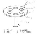
本発明の半導体装置の製法は、図1に反応装置内のプラッター1とその上の凹部に載置されるウェハ状の基板2の部分の斜視説明図が示されているように、基板2をプラッター1上に載置し、プラッター1を図示しないヒータにより加熱して、放射温度計4によりプラッター1の温度を測定しながら反応ガスを反応させて基板2の表面に半導体層をエピタキシャル成長する場合に、プラッター1の少なくとも1か所に放射温度計4により測定する波長の電磁波(赤外線)を透過し、かつ、表面に凹凸を有するモニター用基板5を載置し、そのモニター用基板5の下側のプラッター1からの熱輻射により温度を測定しながらエピタキシャル成長をするものである。
【0018】
プラッター1は、その表面にウェハ状の基板2を載置することができるように、凹部が複数個形成されており、その裏面の中心部には棒状部1aが固定されてモータなどにより回転できるようにされている。プラッター1は、Mo、C、SiCなどの耐熱性の材料からなっている。
【0019】
モニター用基板5は、放射温度計4により測定する波長の電磁波(たとえば1.3μm程度の波長の赤外線)に対して透明な材料からなり、少なくともその表面側に凹凸が形成されており、ザラザラした状態に形成される。この凹凸は、前述の干渉を避けるためのもので、モニター用基板5の屈折率をnとして、放射温度計4により測定する波長の1/(4n)以上、好ましくは1/(4n)〜1/n程度の表面粗さに形成されておればよく、たとえばチッ化ガリウム系化合物半導体層を積層するサファイア基板(厚さが350μm程度)を裏向きにして、裏面のザラザラした面を使用することができる。このモニター用基板5は、エピタキシャル成長用のサファイア基板を用いなくても、放射温度計4により測定する波長の電磁波に対して透明であればよいため、たとえば石英、ガラス、シリコン基板などを使用することができる。また、表面の凹凸は、両面に形成されていてもよく、鏡面仕上げがされていない程度の凹凸があればよいため、厚さが0.35〜1mm程度の通常の石英板やガラス板、シリコン基板などをそのまま使用することができる。
【0020】
本発明により半導体層を基板上に積層するには、MOCVD装置内で、前述のプラッター1の凹部にチッ化ガリウム系化合物半導体を積層するウェハ状の基板2と、少なくとも1個のモニター用基板5とをセッティングする。そして、図1に示されるように、、モニター用基板5上から温度を測定することができるように、放射温度計4をセッティングし、MOCVD装置内をH2 ガス雰囲気にしてプラッター1の下に配設される図示しないヒータによりプラッター1の温度を上昇させ、基板2の温度を上昇させる。そして、たとえば図2に示され、以下に示すように半導体層をエピタキシャル成長して積層する。このときの基板2の温度は、モニター用基板5を介して放射温度計4により測定されるが、プラッター1は図示しないモータにより棒状部1aを介して回転しており、測定に際してはモニター用基板5からの熱輻射による入力の場合のみのデータを使用する。
【0021】
図2に示されるようなチッ化ガリウム系化合物半導体を積層するには、まず、サファイア基板21の温度がたとえば500〜600℃程度になったところで、NH3 と、TMG(トリメチルガリウム)とをキャリアガスのH2 および必要なドーパントガス(n形の場合、たとえばSiH4 、p形の場合、たとえばシクロペンタジエニルマグネシウム)と共に導入して反応させ、GaNからなる低温バッファ層22を0.01〜0.2μm程度程度形成し、ついで基板2の温度をたとえば1000〜1100℃程度にして、同じ組成でn形のn形層(クラッド層)23を1〜2μm程度成膜する。さらに基板2の温度をたとえば700〜800℃程度にして、ドーパントガスを止め、反応ガスとしてTMIn(トリメチルインジウム)を追加し、InGaN系(InとGaの比率が種々変り得ることを意味する)化合物半導体からなる活性層24を0.05〜0.3μm程度成膜する。
【0022】
ついで、基板2の温度を再度たとえば1000〜1100℃程度にして、反応ガスのTMInをTMA(トリメチルアルミニウム)に変更し、ドーパントガスをp形のガスとして、p形のAlGaN系(AlとGaの比率が種々変り得ることを意味する)化合物半導体層を0.1〜0.5μm程度、さらに同じ基板2の温度を維持しながら再度反応ガスのTMAを止めてp形のGaN層を0.1〜0.5μm程度それぞれ積層し、p形層25を形成する。
【0023】
その結果、チッ化ガリウム系化合物半導体からなる発光層形成部が積層される。この後は図示されていないが、アニール処理によりp形層の活性化をして、NiおよびAuの合金層からなる拡散メタル層をたとえば5nm程度形成し、その表面に、および積層した半導体層の一部をエッチング除去することにより露出するn形層23にそれぞれ電極を形成することにより、チッ化ガリウム系化合物半導体からなる青色系の半導体発光素子が得られる。
【0024】
本発明によれば、半導体層をエピタキシャル成長する基板の他に、温度測定のためのモニター用基板をプラッター上に載置して、モニター用基板を介してプラッターの温度を測定している。しかも、モニター用基板は、放射温度計により測定する波長の電磁波(赤外線)に対して透明であると共に、表面に凹凸部が形成されている。このモニター用基板の表面に堆積される半導体層も1工程で積まれる程度の厚さでは、エピタキシャル成長していなくても前述の電磁波に対して透明であり、モニター用基板の下側のプラッターの表面からの輻射により温度を測定することができる。しかも、モニター用基板ではその表面が凹凸になっているため、干渉を起こすような規則的な反射が生ぜず、成長する半導体層の厚さに拘らず、安定した温度測定をすることができる。その結果、基板の温度制御を正確に行うことができ、均一な半導体層を成長することができる。
【0025】
前述の例のように、サファイア基板にチッ化ガリウム系化合物半導体層を積層する場合には、前述のようにプラッターの凹部の1つのサファイア基板を裏向きにするだけで、通常と同様の工程でエピタキシャル成長をすることができ、簡単に均一なチッ化ガリウム系化合物半導体層を成長することができる。
【0026】
なお、モニター用基板は1枚でなくても複数枚設けることもでき、その場合はプラッター上の異なる場所での温度測定を行うことができ、バラツキを抑えるのに都合がよい。この場合、モニター用基板は温度測定のための面積があればよく、通常の基板を載置する凹部とは別にプラッター上に小さな凹部を設けてモニター用基板を載置すれば、エピタキシャル成長する基板の枚数は減らない。また、基板を取り替えた新たなエピタキシャル成長をする度に、モニター用基板を取り替えれば、プラッターの汚れを気にすることなく、常に正確なプラッターの温度を測定することができる。
【0027】
【発明の効果】
本発明によれば、半導体層の成長する厚さに拘らず、常に安定してプラッター、すなわち基板の温度を測定することができ、均一な半導体層のエピタキシャル成長をすることができる。バッチ処理を重ねても再現性よく温度が制御できる。その結果、特性の優れた半導体装置を得ることができる。
【図面の簡単な説明】
【図1】本発明の製法に用いるプラッター上に基板およびモニター用基板を載置した状態の斜視説明図である。
【図2】基板上にチッ化ガリウム系化合物半導体を積層した例の説明図である。
【図3】従来のエピタキシャル成長をするときのプラッター部の説明図である。
【図4】基板上に半導体層を成長するときの反射による干渉の説明図である。
【符号の説明】
1 プラッター
2 基板
4 放射温度計
5 モニター用基板[0001]
BACKGROUND OF THE INVENTION
The present invention relates to a method for manufacturing a semiconductor device capable of performing epitaxial growth while accurately controlling the temperature of a substrate when a semiconductor layer is epitaxially grown on a substrate by, for example, MOCVD (metal organic chemical vapor deposition). More specifically, a semiconductor device that can be epitaxially grown while measuring temperature so as not to cause an error in measurement temperature even by stacking of semiconductor layers, and can be temperature controlled with good reproducibility even after repeated batch processing. It relates to the manufacturing method.
[0002]
[Prior art]
Conventionally, when a semiconductor layer is epitaxially grown on a wafer-like substrate by MOCVD, for example, as shown in FIG. 3, the wafer-
[0003]
For example, when a gallium nitride compound semiconductor is stacked on the
[0004]
[Problems to be solved by the invention]
When the temperature is controlled by the
[0005]
On the other hand, when the temperature is controlled by the above-described
[0006]
[Expression 1]
When the optical path difference between T n and T m (n ≠ m) becomes an integral multiple of the wavelength of thermal radiation due to the increase in film thickness of the gallium nitride compound semiconductor layer, T n and T m interfere, and T When it becomes large and becomes a half integer multiple, it becomes weak. That is, there is a problem that the temperature value measured with the growth of the gallium nitride
[0008]
Although the actual temperature of the
[0009]
In addition, when measuring the temperature by the thermal radiation of the surface of the platter in a portion where there is no substrate, the measurement is performed by the thermal radiation from the uneven deposit layer laminated on the surface. Since emissivity (emissivity) differs with materials such as C, the measurement temperature shifts as reaction by-products accumulate. As a result, in any of the above-described methods, there is a problem that the accurate temperature on the platter cannot be measured and uniform epitaxial growth cannot be performed.
[0010]
The present invention has been made to solve such a problem, and can accurately measure the temperature of a substrate during epitaxial growth to epitaxially grow a uniform crystal layer. An object of the present invention is to provide a method of manufacturing a semiconductor device that realizes a certain temperature control.
[0011]
[Means for Solving the Problems]
In the method of manufacturing a semiconductor device according to the present invention, a substrate is placed on a platter in a reaction apparatus, the platter is heated, and a reaction gas is reacted while measuring the temperature of the platter with a radiation thermometer to thereby react the substrate surface. the semiconductor layer is provided a process for the preparation of semiconductor device epitaxial growth, at least one location of the platter, and transmitting an electromagnetic wave of a wavelength to be measured by the radiation thermometer, and a refractive index of a material of n, the radiation A monitor substrate having unevenness of 1 / (4n) or more of the wavelength measured by a thermometer is placed on the surface , and epitaxial growth is performed while measuring the temperature by thermal radiation from the platter below the monitor substrate. Is.
[0012]
Here, the platter means a mounting table for mounting a substrate on which a semiconductor layer is epitaxially grown in a reaction apparatus.
[0013]
By doing so, the semiconductor layer laminated on the monitor substrate is also transparent to the electromagnetic wave of the measurement wavelength at the thickness of the semiconductor layer laminated by one-step epitaxial growth, and unevenness is formed on the surface thereof. Therefore, the interference between the multiple reflected waves as described above does not occur, and the temperature of the platter surface can be accurately measured. As a result, uniform epitaxial growth can be achieved.
[0015]
In another embodiment of the method for producing a semiconductor device according to the present invention, a sapphire substrate is placed on a platter in a reaction device, the platter is heated, and the reaction gas is reacted while measuring the temperature of the platter with a radiation thermometer. the gallium nitride based compound semiconductor layer on the sapphire substrate surface by a method of a semiconductor device epitaxial growth, at least one location of the platter, as a monitor substrate having unevenness on the front surface, epitaxially growing a semiconductor layer placed by a sapphire base plate face down, characterized in that the epitaxially grown while measuring the temperature by the heat radiation from the platter under side of the monitor board. Here, the gallium nitride compound semiconductor is a compound in which a group III element Ga and a group V element N or a part of the group III element Ga is substituted with another group III element such as Al or In, and A semiconductor composed of a compound in which a part of N of the group V element is substituted with another group V element such as P or As.
If the roughness of the exposed surface of the sapphire substrate placed facing down is not less than 1 / (4n) of the wavelength measured by the radiation thermometer, where n is the refractive index of the sapphire substrate, The influence of radiation interference can be avoided, and the radiant heat of the platter surface below the monitor substrate can be measured without being affected by the semiconductor layer laminated on the surface.
[0016]
DETAILED DESCRIPTION OF THE INVENTION
Next, a method for manufacturing a semiconductor device of the present invention will be described with reference to the drawings.
[0017]
In the method of manufacturing a semiconductor device of the present invention, as shown in FIG. 1, a perspective view of a portion of a wafer-
[0018]
The
[0019]
The
[0020]
In order to stack a semiconductor layer on a substrate according to the present invention, a wafer-
[0021]
In order to stack the gallium nitride compound semiconductor as shown in FIG. 2, first, when the temperature of the
[0022]
Next, the temperature of the
[0023]
As a result, a light emitting layer forming portion made of a gallium nitride compound semiconductor is stacked. After this, although not shown in the figure, the p-type layer is activated by annealing to form a diffusion metal layer made of an alloy layer of Ni and Au, for example, about 5 nm, on the surface, and on the laminated semiconductor layer. By forming electrodes on the n-type layer 23 exposed by etching away a part, a blue semiconductor light emitting element made of a gallium nitride compound semiconductor can be obtained.
[0024]
According to the present invention, in addition to the substrate on which the semiconductor layer is epitaxially grown, a monitor substrate for temperature measurement is placed on the platter, and the temperature of the platter is measured via the monitor substrate. Moreover, the monitor substrate is transparent to electromagnetic waves (infrared rays) having a wavelength measured by a radiation thermometer, and has an uneven portion on the surface. The thickness of the semiconductor layer deposited on the surface of the monitor substrate is transparent to the above-described electromagnetic wave even if it is not epitaxially grown, and the surface of the platter below the monitor substrate. The temperature can be measured by radiation from. Moreover, since the surface of the monitor substrate is uneven, regular reflection that causes interference does not occur, and stable temperature measurement can be performed regardless of the thickness of the growing semiconductor layer. As a result, the substrate temperature can be accurately controlled, and a uniform semiconductor layer can be grown.
[0025]
As described above, when a gallium nitride compound semiconductor layer is stacked on a sapphire substrate, the sapphire substrate in the concave portion of the platter is simply turned face down as described above, and the same process as usual is performed. Epitaxial growth can be performed, and a uniform gallium nitride compound semiconductor layer can be easily grown.
[0026]
Note that a plurality of monitor substrates may be provided instead of one, and in this case, temperature measurement can be performed at different locations on the platter, which is convenient for suppressing variations. In this case, the monitor substrate only needs to have an area for temperature measurement. If the monitor substrate is placed with a small recess on the platter in addition to the recess where the normal substrate is placed, the substrate for epitaxial growth can be obtained. The number is not reduced. If the monitor substrate is replaced each time a new epitaxial growth is performed after replacing the substrate, the accurate platter temperature can always be measured without worrying about contamination of the platter.
[0027]
【The invention's effect】
According to the present invention, the temperature of the platter, that is, the substrate can be measured stably regardless of the growth thickness of the semiconductor layer, and a uniform semiconductor layer can be epitaxially grown. Even if batch processing is repeated, the temperature can be controlled with good reproducibility. As a result, a semiconductor device having excellent characteristics can be obtained.
[Brief description of the drawings]
FIG. 1 is an explanatory perspective view of a state in which a substrate and a monitor substrate are placed on a platter used in the manufacturing method of the present invention.
FIG. 2 is an explanatory view of an example in which a gallium nitride compound semiconductor is stacked on a substrate.
FIG. 3 is an explanatory diagram of a platter portion when performing conventional epitaxial growth.
FIG. 4 is an explanatory diagram of interference caused by reflection when a semiconductor layer is grown on a substrate.
[Explanation of symbols]
1
Claims (3)
Priority Applications (1)
| Application Number | Priority Date | Filing Date | Title |
|---|---|---|---|
| JP22470097A JP3649867B2 (en) | 1997-08-21 | 1997-08-21 | Manufacturing method of semiconductor devices |
Applications Claiming Priority (1)
| Application Number | Priority Date | Filing Date | Title |
|---|---|---|---|
| JP22470097A JP3649867B2 (en) | 1997-08-21 | 1997-08-21 | Manufacturing method of semiconductor devices |
Publications (2)
| Publication Number | Publication Date |
|---|---|
| JPH1167672A JPH1167672A (en) | 1999-03-09 |
| JP3649867B2 true JP3649867B2 (en) | 2005-05-18 |
Family
ID=16817882
Family Applications (1)
| Application Number | Title | Priority Date | Filing Date |
|---|---|---|---|
| JP22470097A Expired - Fee Related JP3649867B2 (en) | 1997-08-21 | 1997-08-21 | Manufacturing method of semiconductor devices |
Country Status (1)
| Country | Link |
|---|---|
| JP (1) | JP3649867B2 (en) |
Families Citing this family (3)
| Publication number | Priority date | Publication date | Assignee | Title |
|---|---|---|---|---|
| JP3956637B2 (en) | 2001-04-12 | 2007-08-08 | ソニー株式会社 | Nitride semiconductor crystal growth method and semiconductor element formation method |
| JP5730638B2 (en) * | 2011-03-28 | 2015-06-10 | 東京エレクトロン株式会社 | Process chamber constituent member of substrate processing apparatus and temperature measuring method thereof |
| CN103389170B (en) * | 2012-05-07 | 2015-08-19 | 中微半导体设备(上海)有限公司 | A kind of substrate temperature measuring method of vacuum treatment installation and device |
-
1997
- 1997-08-21 JP JP22470097A patent/JP3649867B2/en not_active Expired - Fee Related
Also Published As
| Publication number | Publication date |
|---|---|
| JPH1167672A (en) | 1999-03-09 |
Similar Documents
| Publication | Publication Date | Title |
|---|---|---|
| CN102598239B (en) | Method for improving the performance of a substrate carrier | |
| US9064696B2 (en) | Apparatus for manufacturing compound semiconductor, method for manufacturing compound semiconductor, and compound semiconductor | |
| US20060226414A1 (en) | Group III-V nitride-based semiconductor substrate and method of making same | |
| JP6062436B2 (en) | Susceptor, crystal growth apparatus and crystal growth method | |
| KR20160061340A (en) | Method and apparatus for forming device quality gallium nitride layers on silicon substrates | |
| JP2016533645A5 (en) | Method for forming a device quality gallium nitride layer on a silicon substrate | |
| JP2019009329A (en) | Method for measuring film thickness, method for producing nitride semiconductor laminate, and nitride semiconductor laminate | |
| JP3954335B2 (en) | Group III nitride multilayer film | |
| EP2312616B1 (en) | Film deposition method | |
| JP3649867B2 (en) | Manufacturing method of semiconductor devices | |
| JPH10284425A (en) | Manufacture of semiconductor device | |
| US20130019927A1 (en) | Use of freestanding nitride veneers in semiconductor devices | |
| CN111286781A (en) | RAMO4 substrate, method for manufacturing the same, and group III nitride semiconductor | |
| Kuan et al. | Dislocation mechanisms in the GaN lateral overgrowth by hydride vapor phase epitaxy | |
| CN103094424A (en) | Wafer carrier | |
| JP2012101977A (en) | Method for manufacturing nitride semiconductor substrate, and method for manufacturing nitride semiconductor self-standing substrate | |
| WO2016194931A1 (en) | In-situ observation device of substrate warpage and crystal growth apparatus | |
| JP2019009426A (en) | Method for measuring film thickness, method for producing nitride semiconductor laminate, and nitride semiconductor laminate | |
| JP3763685B2 (en) | Epitaxial wafer and evaluation method thereof | |
| JP3104677B2 (en) | Group III nitride crystal growth equipment | |
| JPH08250425A (en) | Substrates and methods for vapor deposition of semiconductors and other materials | |
| JPH0258322A (en) | Method of manufacturing semiconductor wafers | |
| JPH11251249A (en) | Method of forming semiconductor film | |
| JPS63197326A (en) | Formation of compound semiconductor substrate | |
| JPS62123093A (en) | Mounting of substrate on molecular beam epitaxial growth apparatus |
Legal Events
| Date | Code | Title | Description |
|---|---|---|---|
| A977 | Report on retrieval |
Free format text: JAPANESE INTERMEDIATE CODE: A971007 Effective date: 20040601 |
|
| A131 | Notification of reasons for refusal |
Free format text: JAPANESE INTERMEDIATE CODE: A131 Effective date: 20040629 |
|
| A521 | Written amendment |
Free format text: JAPANESE INTERMEDIATE CODE: A523 Effective date: 20040830 |
|
| A131 | Notification of reasons for refusal |
Free format text: JAPANESE INTERMEDIATE CODE: A131 Effective date: 20041019 |
|
| A521 | Written amendment |
Free format text: JAPANESE INTERMEDIATE CODE: A523 Effective date: 20041220 |
|
| TRDD | Decision of grant or rejection written | ||
| A01 | Written decision to grant a patent or to grant a registration (utility model) |
Free format text: JAPANESE INTERMEDIATE CODE: A01 Effective date: 20050208 |
|
| A61 | First payment of annual fees (during grant procedure) |
Free format text: JAPANESE INTERMEDIATE CODE: A61 Effective date: 20050216 |
|
| R150 | Certificate of patent or registration of utility model |
Free format text: JAPANESE INTERMEDIATE CODE: R150 |
|
| FPAY | Renewal fee payment (event date is renewal date of database) |
Free format text: PAYMENT UNTIL: 20080225 Year of fee payment: 3 |
|
| FPAY | Renewal fee payment (event date is renewal date of database) |
Free format text: PAYMENT UNTIL: 20110225 Year of fee payment: 6 |
|
| FPAY | Renewal fee payment (event date is renewal date of database) |
Free format text: PAYMENT UNTIL: 20110225 Year of fee payment: 6 |
|
| FPAY | Renewal fee payment (event date is renewal date of database) |
Free format text: PAYMENT UNTIL: 20120225 Year of fee payment: 7 |
|
| FPAY | Renewal fee payment (event date is renewal date of database) |
Free format text: PAYMENT UNTIL: 20130225 Year of fee payment: 8 |
|
| LAPS | Cancellation because of no payment of annual fees |