JP3649841B2 - Single plate color camera - Google Patents
Single plate color camera Download PDFInfo
- Publication number
- JP3649841B2 JP3649841B2 JP03620397A JP3620397A JP3649841B2 JP 3649841 B2 JP3649841 B2 JP 3649841B2 JP 03620397 A JP03620397 A JP 03620397A JP 3620397 A JP3620397 A JP 3620397A JP 3649841 B2 JP3649841 B2 JP 3649841B2
- Authority
- JP
- Japan
- Prior art keywords
- color
- signal
- rows
- columns
- photoelectric conversion
- Prior art date
- Legal status (The legal status is an assumption and is not a legal conclusion. Google has not performed a legal analysis and makes no representation as to the accuracy of the status listed.)
- Expired - Fee Related
Links
- 238000012545 processing Methods 0.000 claims description 39
- 238000006243 chemical reaction Methods 0.000 claims description 30
- 238000000034 method Methods 0.000 claims description 29
- 238000000926 separation method Methods 0.000 claims description 25
- 238000003384 imaging method Methods 0.000 claims description 13
- 230000000295 complement effect Effects 0.000 claims description 12
- 239000003086 colorant Substances 0.000 claims description 10
- 238000012937 correction Methods 0.000 claims description 7
- 238000012935 Averaging Methods 0.000 claims description 6
- 230000000875 corresponding effect Effects 0.000 description 37
- 238000010586 diagram Methods 0.000 description 28
- 230000007274 generation of a signal involved in cell-cell signaling Effects 0.000 description 23
- 238000012546 transfer Methods 0.000 description 14
- 230000003287 optical effect Effects 0.000 description 7
- 230000007423 decrease Effects 0.000 description 5
- 102100034289 Deoxynucleoside triphosphate triphosphohydrolase SAMHD1 Human genes 0.000 description 4
- 101000641031 Homo sapiens Deoxynucleoside triphosphate triphosphohydrolase SAMHD1 Proteins 0.000 description 4
- 238000009825 accumulation Methods 0.000 description 4
- 238000003491 array Methods 0.000 description 4
- 230000003111 delayed effect Effects 0.000 description 3
- 230000004044 response Effects 0.000 description 3
- 230000001934 delay Effects 0.000 description 2
- 230000014509 gene expression Effects 0.000 description 2
- 238000005070 sampling Methods 0.000 description 2
- 125000002015 acyclic group Chemical group 0.000 description 1
- 239000000654 additive Substances 0.000 description 1
- 230000000996 additive effect Effects 0.000 description 1
- 238000013459 approach Methods 0.000 description 1
- 230000002596 correlated effect Effects 0.000 description 1
- 230000000694 effects Effects 0.000 description 1
- 238000001914 filtration Methods 0.000 description 1
- 230000005484 gravity Effects 0.000 description 1
- 230000007246 mechanism Effects 0.000 description 1
- 230000035945 sensitivity Effects 0.000 description 1
Images


Classifications
-
- H—ELECTRICITY
- H10—SEMICONDUCTOR DEVICES; ELECTRIC SOLID-STATE DEVICES NOT OTHERWISE PROVIDED FOR
- H10F—INORGANIC SEMICONDUCTOR DEVICES SENSITIVE TO INFRARED RADIATION, LIGHT, ELECTROMAGNETIC RADIATION OF SHORTER WAVELENGTH OR CORPUSCULAR RADIATION
- H10F39/00—Integrated devices, or assemblies of multiple devices, comprising at least one element covered by group H10F30/00, e.g. radiation detectors comprising photodiode arrays
- H10F39/10—Integrated devices
- H10F39/12—Image sensors
-
- H—ELECTRICITY
- H04—ELECTRIC COMMUNICATION TECHNIQUE
- H04N—PICTORIAL COMMUNICATION, e.g. TELEVISION
- H04N23/00—Cameras or camera modules comprising electronic image sensors; Control thereof
- H04N23/80—Camera processing pipelines; Components thereof
- H04N23/84—Camera processing pipelines; Components thereof for processing colour signals
- H04N23/843—Demosaicing, e.g. interpolating colour pixel values
-
- H—ELECTRICITY
- H04—ELECTRIC COMMUNICATION TECHNIQUE
- H04N—PICTORIAL COMMUNICATION, e.g. TELEVISION
- H04N25/00—Circuitry of solid-state image sensors [SSIS]; Control thereof
- H04N25/10—Circuitry of solid-state image sensors [SSIS]; Control thereof for transforming different wavelengths into image signals
- H04N25/11—Arrangement of colour filter arrays [CFA]; Filter mosaics
- H04N25/13—Arrangement of colour filter arrays [CFA]; Filter mosaics characterised by the spectral characteristics of the filter elements
- H04N25/135—Arrangement of colour filter arrays [CFA]; Filter mosaics characterised by the spectral characteristics of the filter elements based on four or more different wavelength filter elements
- H04N25/136—Arrangement of colour filter arrays [CFA]; Filter mosaics characterised by the spectral characteristics of the filter elements based on four or more different wavelength filter elements using complementary colours
-
- H—ELECTRICITY
- H04—ELECTRIC COMMUNICATION TECHNIQUE
- H04N—PICTORIAL COMMUNICATION, e.g. TELEVISION
- H04N2209/00—Details of colour television systems
- H04N2209/04—Picture signal generators
- H04N2209/041—Picture signal generators using solid-state devices
- H04N2209/042—Picture signal generators using solid-state devices having a single pick-up sensor
- H04N2209/045—Picture signal generators using solid-state devices having a single pick-up sensor using mosaic colour filter
- H04N2209/046—Colour interpolation to calculate the missing colour values
Landscapes
- Engineering & Computer Science (AREA)
- Multimedia (AREA)
- Signal Processing (AREA)
- Physics & Mathematics (AREA)
- Spectroscopy & Molecular Physics (AREA)
- Color Television Image Signal Generators (AREA)
Description
【0001】
【発明の属する技術分野】
この発明は、カラーカメラに関し、特に、色差順次方式によりアレイ状に配列された色フィルタに対応して、アレイ状に配置される光電変換素子を含む固体撮像デバイスからの信号を処理する色分離回路を有する単板式カラーカメラに関する。
【0002】
【従来の技術】
カラーカメラにおいて、現在撮像デバイスとして広く用いられているCCD(Charge Coupled Device )は、受けた光の明暗に応じて出力する信号の振幅を変化させるだけで、その出力信号にはカラー情報が含まれない。したがって、カラー情報を得るためには光学的な手段を用いて、CCDに入射する光にフィルタをかける等の工夫が必要となる。
【0003】
家庭用のカラーカメラにおいては、単一のCCDから三原色信号を取出す、いわゆる単板式方式が採用され、このCCDの受光面側に色フィルタアレイを用いた、いわゆる同時式のカラー撮像方式が採用されている。
【0004】
[インターライン転送CCDの構成]
図10は、家庭用カラーカメラにおけるCCDの構成として、一般に用いられているインターライン転送CCD10の構成を示す概略ブロック図である。
【0005】
インターライン転送CCD10は、アレイ状に配置されたpn接合型フォトダイオードからなる感光部12と、CCDにより構成されるアナログシフトレジスタを含む転送部14と、転送部14により転送された電荷を受けて、順次転送された信号電荷を電圧に変換した信号を水平方向に転送して出力する水平転送レジスタ16とを含む。
【0006】
図10においては、簡単のためpn接合型フォトダイオードは、垂直水平とも3画素が配置された構成としている。実際に、カラーカメラに使用されるCCDでは、たとえば、垂直方向に500画素、水平方向には500〜800画素に対応するフォトダイオードがアレイ状に配置されている。
【0007】
次に、その動作について簡単に説明する。
フォトダイオードに光が入射すると電荷が発生し、ダイオード内に蓄積されていく。次に、シフトゲートに所定の電圧を印加することにより、蓄積された電荷は一斉にアナログシフトレジスタ14に転送される。CCDアナログシフトレジスタ14は、クロックパルス電圧φV1,φV2,φV3が印加されることにより、電荷を順次水平転送レジスタ16に向かって転送していく。水平転送レジスタ16では、送られてきた信号電荷を電圧に変換した後、外部から与えられる水平駆動信号φH1,φH2,φH3に駆動されて、順次撮像信号出力として外部に出力する。
【0008】
[インターライン転送CCDの駆動方式]
インターライン転送CCDの駆動方法としては、一般にフレーム蓄積方式とフィールド蓄積方式の2つのモードが存在する。カラーカメラにおいては、色差順次方式の色フィルタアレイに対応しても、全画素読み出し動作を前提としたフレーム蓄積方式が用いられる場合がある。
【0009】
以下では、インターライン転送CCDは、1画素ごとに読み出すことが可能なフレーム蓄積モードで動作している場合について考えることにする。
【0010】
[色差信号の分離方式]
図11は、色差順次方式で配列されている色フィルタアレイの構成を示す模式図である。
【0011】
図11に示すように、色差順次方式の色フィルタにおいては、色フィルタとしてマゼンダ(以下、Mgで表わす),緑色(以下、Gで表わす),シアン(以下、Cyで表わす),黄色(以下、Yeで表わす)の色フィルタがモザイク状に配置されている。
【0012】
ここで、光の色の混合においては、いわゆる加色法が成り立つので、三原色である赤(R),緑(G),青(B)に対して、補色関係にあるMg,Ye,Cyとの間には以下の関係が成り立つ。
【0013】
Mg=R+B …(1)
Ye=R+G …(2)
Cy=B+G …(3)
したがって、色フィルタの色として、上記のMg,G,Ye,Cyを用いることで、三原色のR,G,Bのうち輝度信号に対して大きな比重を有するG信号の強度をR信号およびB信号よりも大きくとることが可能となる。
【0014】
図11に示した例においては、色差順次方式の色フィルタアレイのうち、4行4列のアレイ部分を抜き出して示している。奇数番目の行(x=1、3)においてはGの色フィルタとMgの色フィルタが水平方向(y方向)に交互に配置されている。
【0015】
一方、偶数番目の行(x=0、2)においてはYeの色フィルタとCyの色フィルタとが水平方向に交互に配置される構成となっている。
【0016】
図12は、図11に示した4行4列の色フィルタの配列が、水平方向に1画素分だけずれた場合の色フィルタの配列を示す。
【0017】
たとえば、光電変換素子からの出力をy方向に順次読み出す場合、ある時点でCCDから読み出された4行4列分の光電変換素子からの出力は、図11に示す色フィルタアレイからの出力に対応する場合と、図12に示す色フィルタアレイからの出力に対応する場合とが交互に繰り返されることになる。図11に示すような色差順次方式の色フィルタの配列では、任意の4行4列の色フィルタの配列は図11または図12に示した場合のほか、図11または図12の配置をそれぞれx方向に1画素分ずらせた場合とを合わせた4通りの配列のいづれかとなる。
【0018】
図13は、従来の色分離方式を説明するための概念図である。図13では、図11に示した4行4列の配列のうち2行2列を抜き出して示す。従来の色分離方式においては、CCDから全画素読み出しにより得られた信号のうち、このような2行2列の画素に対応する信号から、2行2列の画素の中央位置についての輝度信号Y、第1の色差信号Cb、第2の色差信号Crを生成する。
【0019】
ここで、輝度信号Y、第1の色差信号Cb、第2の色差信号Crは、三原色に対応する信号強度をそれぞれR、G、Bとするとき、以下の式で表現される信号である。
【0020】
【0021】
G=(2Y−2Cr−2Cb)/10 …(7)
R=(Y+4Cr−Cb)/10 …(8)
B=(Y−Cr+4Cb)/10 …(9)
【0022】
【発明が解決しようとする課題】
しかしながら、上述したような色分離方式では以下に説明するような問題点が存在する。
【0023】
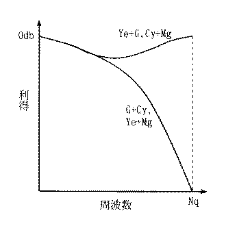
図14は、図13に示すような従来の色分離方式をデジタルフィルタにより実現した場合の出力信号Ye+G,Cy+Mg,G+Cy,Ye+Mgの水平方向の周波数特性を示す図である。
【0024】
図13において、CCDからの信号の読み出しが、y方向に順次行われるとすると、信号Ye+G,Cy+Mgについては同一時点でサンプリングされた信号から生成されるのに対し、信号G+Cy,Ye+Mgについては、1サンプリング時間だけ信号をホールドすることが必要となる。
【0025】
このため、信号Ye+G,Cy+Mgの利得は周波数依存性を持たないのに対し、信号G+Cy,Ye+Mgはナイキスト周波数に近づくにしたがって、単調に利得が減少するという特性を示す。
【0026】
このような第1および第2の色差信号Cb、Crを生成するもととなる信号の水平方向の周波数特性が異なると、偽色信号が発生し、画質を損なってしまうという問題があった。
【0027】
本発明は、上記のような問題点を解決するためになされたものであって、その目的は、各色成分信号の帯域をそろえ、偽色信号の発生を抑制して画質を向上させることが可能な単板式カラーカメラを提供することである。
【0028】
この発明の他の目的は、各色信号成分の帯域をそろえた場合でも、解像度の低下を抑制するすることが可能な単板式カラーカメラを提供することである。
【0029】
【課題を解決するための手段】
請求項1記載の単板式カラーカメラは、画素に各々対応する光電変換素子が、アレイ状に配列された固体撮像手段を備え、固体撮像手段は、受光面側に、対応する光電変換素子に対して色差順次方式で色フィルタがモザイク状に配列される色フィルタアレイを含み、任意の4行4列の画素に対応して、色フィルタアレイの4行4列の偶数番目の行は、交互に配置される緑色フィルタおよびマゼンダに対応する第1の補色フィルタを有し、4行4列の奇数番目の行は、交互に配置される黄色に対応する第2の補色フィルタおよびシアンに対応する第3の補色フィルタを有し、固体撮像手段の出力を4行ごとに順次受けて、4行4列の画素の中央位置に対応する色データを生成する色分離手段をさらに備え、色分離手段は、緑色ならびに第1ないし第3の補色のそれぞれについて、順次受け取る4行4列の画素に対応する複数の光電変換素子からの出力のうち、対応する色フィルタの配置された光電変換素子からの出力を加重平均して出力する色補間手段と、色補間手段からの出力を受けて、中央位置に対応する色データを分離する第1の演算手段とを含み、4行4列の画素に対応する光電変換素子からの出力をD(x、y)(x=0〜3、y=0〜3)とし、加重平均処理において、D(x、y)に対応する重み付け係数をw(x、y)とするとき、色補間手段は、第1の重み付け係数として、w(1,2)=2,w=(1,0)=1およびw(3,2)=1とする第1の加重平均処理、第2の重み付け係数として、w(1,1)=2,w=(3,1)=1およびw(1,3)=1とする第2の加重平均処理、第3の重み付け係数として、w(2,2)=2,w=(0,2)=1およびw(2,0)=1とする第3の加重平均処理および第4の重み付け係数として、w(2,1)=2,w=(2,3)=1およびw(0,1)=1とする第4の加重平均処理を、順次受け取る4行4列の画素に対応する色フィルタの配列に応じて、緑色ならびに第1ないし第3の補色に対してそれぞれ実行する。
【0032】
請求項2記載の単板式カラーカメラは、請求項1記載の単板式カラーカメラの構成において、色分離手段は、4行4列の画素に対応する光電変換素子からの出力のうち、中央位置を囲む2行2列の光電変換素子からの出力を加算することで輝度信号を出力する第2の演算手段を含む。
【0033】
請求項3記載の単板式カラーカメラは、請求項2記載の単板式カラーカメラの構成において、4行4列の画素に対応する光電変換素子からの出力のうち、D(0,1)、D(0,2)、D(1,1)およびD(1,2)の和である第1の信号と、D(1,0)、D(1,1)、D(2,0)およびD(2,1)の和である第2の信号と、D(2,1)、D(2,2)、D(3,1)およびD(3,2)の和である第3の信号と、D(1,2)、D(1,3)、D(2,2)およびD(2,3)の和である第4の信号と、輝度信号とに基づいてアパーチャ信号を出力するアパーチャ信号生成手段と、アパーチャ信号に応じて、アパーチャ補正を行う補正手段とをさらに備える。
【0034】
【発明の実施の形態】
図1は、本発明の実施の形態の単板式カラーカメラの構成のうち、撮像素子であるCCD10に撮像対象の光学像を結ぶ光学系2から色分離回路100までを含む色信号処理系1000の構成を示す概略ブロック図である。
【0035】
色信号処理系1000は、撮像対象の光を受ける光学系2と、光学系2により結像された光学像を電気信号に変換するCCD10と、CCD10に対して全画素独立読出駆動を行なう駆動回路40と、CCD10の出力信号を受けて、撮像信号から周知の方法でノイズ除去を行う相関2重サンプリング回路(以下、CDS回路と呼ぶ)44と、CDS回路44の出力を増幅するオートゲインコントロール回路(以下、AGC回路と呼ぶ)46と、AGC回路46の出力をデジタル信号に変換するA/D変換回路48と、A/D変換回路48からのCCD10の偶数ラインの出力信号と奇数ラインの出力信号を入れ子状に保持するフレームメモリ50と、駆動回路40からのCCD駆動信号を受けて、出力信号が読み出される画素の水平アドレスHA,垂直アドレスVAを出力する制御回路42を含む。
【0036】
色信号処理系1000は、さらに、フレームメモリ50からの第1入力信号を1走査線時間分だけ遅延して第2入力信号を出力する走査線遅延器18と、第2入力信号を1走査線時間分だけ遅延して第3入力信号を出力する走査線遅延器20と、第3入力信号を1走査線時間分だけ遅延して第4入力信号を出力する走査線遅延器22と、第1〜第4入力信号を受けて、輝度信号Y、第1の色差信号Cb、第2の色差信号Crを出力する2次元非巡回型デジタルフィルタである色分離回路100とを含む。
【0037】
色分離回路100は、第1〜第4入力信号を並列に順次受けて、4行4列分の画素からのデータ(その時点で信号の読み出されたCCDの色フィルタの配列に対応して、緑色、黄色、シアン、マゼンダの色信号を含む。)を保持する2次元レジスタアレイ30と、2次元レジスタアレイ30からの信号を受けて、緑色、黄色、シアン、マゼンダの各色信号ごとに加重平均処理を行うことで、4行4列の画素の中央位置に対応する色信号を補間生成する補間処理回路34と、補間により生成された色信号から色差信号Cb、Crを生成する色差信号生成回路36と、2次元レジスタアレイ30からの信号を受けて、輝度信号Yを生成する輝度信号生成回路32と、輝度信号Yおよび2次元レジスタアレイ30からの信号を受けてアパーチャ信号APを出力するアパーチャ信号生成回路38とを含む。
【0038】
ここで、光学系2に含まれる撮像レンズは、通常、絞り、フォーカス、ズーム等の可変機構を備える。
【0039】
色信号処理系1000は、さらに、アパーチャ信号に応じてアパーチャ補正(輪郭強調処理)を行うアパーチャ補正回路(図示せず)を含む。
【0040】
以上の構成において、第1から第4の4種類の入力信号は、4走査線分(4ライン分)の撮像信号に該当し、これらの信号は4ライン1まとめにして色分離回路100に入力されることになる。
【0041】
こうして、色分離回路100と3個の走査線遅延器18〜22により、FIR(Finite Impulse Response )フィルタが実現される。
【0042】
[補間処理および色分離処理]
図2は、本実施の形態における補間処理動作を説明するための模式図である。図2(a)は、4行4列の色フィルタアレイの配列の一例を示し、図2(b)は、図2(a)のマゼンダ色フィルタの配列の場合の補間処理時の重付け係数の配置を示し、図2(c)は、図2(a)の緑色フィルタの配列の場合の補間処理時の重付け係数の配置を示し、図2(d)は、図2(a)のシアン色フィルタの配列の場合の補間処理時の重付け係数の配置を示し、図2(e)は、図2(a)の黄色フィルタの配列の場合の補間処理時の重付け係数の配置を示す。
【0043】
すなわち、本実施の形態においては、以下の加重平均による補間処理により、4行4列の画素の中央位置に対応するマゼンダ色信号成分、緑色信号成分、シアン色信号成分および黄色信号成分を生成する。
【0044】
Mg=2×Mg11+Mg13+Mg31 …(10)
G =2×G12 +G10 +G32 …(11)
Cy=2×Cy21+Cy01+Cy23 …(12)
Ye=2×Ye22+Ye02+Ye20 …(13)
なお、図11および図12において説明したとおり、4行4列の画素に対応した色フィルタの配列は4種類あり、図2(a)以外の配列の場合は、それに応じて、各色フィルタに対する加重平均の重付け係数の配列も図2(b)〜(e)の中の他の配列にそれぞれ対応することになる。
【0045】
前述したとおり、本実施の形態では、CCD10は全画素独立読出動作を行なう。すなわち、図2(a)に示すように、垂直方向(x方向)0番目の第0ラインについては、水平方向(y方向)に色フィルタYeおよびCyが交互に配置されることに対応して、CCD10からの読出信号は、このラインに対応する走査線については、YeとCyとが交互に出力される信号となる。次の第1ライン(x=1に相当)については、信号Mgと信号Gとが交互に出力される。
【0046】
図3は、図1に示した構成のうち、このようなCCD10からの読み出し信号を受ける走査線遅延回路18、20、22および2次元レジスタアレイ30の構成をさらに詳しく示すブロック図である。
【0047】
2次元レジスタアレイ30は、A/D変換器16からの出力信号を保持するフレームメモリ50からの出力を受け、1クロック分遅延して信号d01を出力するレジスタ302と、信号d01を受けて1クロック分遅延して信号d01を出力するレジスタ302とを含む。
【0048】
2次元アレイレジスタ30は、さらに、走査線遅延器18からの信号d10を受けて、1クロック分遅延して信号d11を出力するレジスタ306と、信号d11を受けて1クロック分遅延して信号d12を出力するレジスタ308と、信号d12を受けて1クロック分遅延して信号d13を出力するレジスタ310と、走査線遅延器20からの信号d20を受けて、1クロック分遅延して信号d21を出力するレジスタ312と、信号d21を受けて1クロック分遅延して信号d22を出力するレジスタ314と、信号d22を受けて1クロック分遅延して信号d23を出力するレジスタ316と、走査線遅延器22からの信号を受けて、1クロック分遅延して信号d31を出力するレジスタ318と、信号d31を受けて1クロック分遅延して信号d32を出力するレジスタ320とを含む。
【0049】
すなわち、二次元レジスタアレイ30により、シリアルに読み出されたCCD10からの信号は、4行4列の画素に対応する光電変換素子からの信号がそれぞれ並列に出力されるように変換される。
【0050】
つまり、上述した信号d01〜d32は、CCD10中の画素(x,y)に対応する光電変換素子からの出力信号を、記号dxyで表わしたことに相当する。
【0051】
図4は、図1に示した補間処理回路34の構成をより詳しく示すブロック図である。
【0052】
補間処理回路34は、信号d12,d10,d32を受けて第1の補間信号を出力する補間演算部342と、信号d11,d13,d31を受けて第2の補間信号を出力する補間演算部344と、信号d21,d01,d23を受けて第3の補間信号を出力する補間演算部346と、信号d22,d02,d20を受けて第4の補間信号を出力する補間演算部348と、制御回路42に制御されて、第1〜第4の補間信号のそれぞれを、緑色信号G、シアン色信号Cy、マゼンダ色信号Mgおよび黄色信号Yeとして出力する選択回路350とを含む。
【0053】
ここで、補間演算部342は、信号d12を受けて2倍にして出力する乗算器3422と、信号d10および信号d32の加算結果を出力する加算器3424と、加算器3424と乗算器3422の加算結果を第1の補間信号として出力する加算器3426とを含む。補間演算部344、346および348の構成も、受ける信号が異なる以外、基本的に補間演算部342の構成と同様である。
【0054】
したがって、補間演算部342は、色フィルタの配置が図2(a)である場合、図2(c)に示した重付け係数の配置による加重平均処理を行うことに対応し、補間演算部344は図2(b)に示した重付け係数の配置による加重平均処理を行うことに、補間演算部346は図2(d)に示した重付け係数の配置による加重平均処理を行うことに、補間演算部348は図2(e)に示した重付け係数の配置による加重平均処理を行うことに、それぞれ対応する。
【0055】
選択回路350は、制御回路42から出力されるCCD10からの現在の読み出し位置を示す水平アドレスHAの最下位ビットh−addLSBおよび垂直アドレスVAの最下位ビットv−addLSBに応じて、第1〜第4の補間信号と緑色信号G、シアン色信号Cy、マゼンダ色信号Mgおよび黄色信号Yeとの対応づけを切り換えて出力する。
【0056】
たとえば、色フィルタが図2(a)である場合は、第1の補間信号が緑色信号Gに、第2の補間信号がマゼンダ色信号Mgに、第3の補間信号がシアン色信号Cyに、第4の補間信号が黄色信号Yeにそれぞれ対応するため、選択回路350は、このような対応づけとなるように信号を出力する。
【0057】
信号を読み出す4行4列の画素に対応する色フィルタの配列が変化した場合は、それに応じて、選択回路350は上述した対応づけを変化させる。
【0058】
以上の補間処理回路34の動作により、緑色信号G、シアン色信号Cy、マゼンダ色信号Mgおよび黄色信号Yeのそれぞれについて、4行4列の画素に対応する光電変換素子からの読み出し信号に対する所定の加重平均処理により、4行4列の画素の中央位置に対応した信号が生成されることになる。
【0059】
図5は、図4に示すようなデジタルフィルタにより補間処理を実現した場合の出力信号Ye+G,Cy+Mg,G+Cy,Ye+Mgの周波数特性を示す図であり、図14と対比される図である。
【0060】
補間処理により、出力信号Ye+G,Cy+Mg,G+Cy,Ye+Mgの周波数特性が1/2ナイキスト周波数付近までそろっている。このため、これらの信号に基づいて色分離処理を行い色差信号CbおよびCrを得た場合、偽色の発生を抑制することが可能で、画質を向上させることができる。
【0061】
なお、以上の説明では、4行4列の画素に対応する光電変換素子からの出力信号に対して図2(b)〜(e)で示される重付け係数の配置の加重平均による補間処理を行う場合について説明したが、本発明はこのような場合に限定されない。たとえば、補間処理を行う対象となる画素は、より一般に、kを偶数とするとき、k行k列の画素であってもかまわない。また、重付け係数の配置も、4つの色信号、すなわち緑色信号、シアン色信号、マゼンダ色信号および黄色信号のそれぞれに対応する重付け係数の配置が、中央位置に対して相互に90度づつ回転した関係となっていればよい。
【0062】
さらに、色信号についても、必ずしも、緑色信号、シアン色信号、マゼンダ色信号および黄色信号に限定されることなく、他の色信号の組み合わせ、たとえばフレーム色差順次方式の色フィルタで用いられるYM、CG、YG、CMの組み合わせに対して適用することも可能である。
【0063】
図6は、図1に示した色差信号生成回路36の構成をより詳しく示すブロック図である。
【0064】
図6を参照して、色差信号生成回路36は、黄色信号Yeとマゼンダ信号Mgを受けて加算する加算器362と、緑信号Gとシアン信号Cyとを受けて加算する加算器368と、加算器368の出力に−1を乗算する乗算器374と、加算器362の出力と乗算器374の出力を加算して信号Crを出力する加算機376とを含む。
【0065】
色差信号生成回路36は、さらに、マゼンダ信号Mgとシアン色信号Cyとを受けて加算する加算器364と、緑信号Gと黄色信号Yeとを受けて加算する加算器366と、加算器366の出力に−1を乗算する乗算器372と、加算器364の出力と乗算器372の出力を加算して信号Cbを出力する加算機370とを含む。
【0066】
すなわち、 色差信号生成回路36は、以下に示す演算処理により、緑色信号G、シアン色信号Cy、マゼンダ色信号Mgおよび黄色信号Yeから色差信号CbおよびCrを生成する。
【0067】
ここで、輝度信号としては、上記補間処理により得られた緑色信号G、シアン色信号Cy、マゼンダ色信号Mgおよび黄色信号Yeから以下の演算により、生成する構成とすることも可能である。
【0068】
【0069】
補間処理を行うことで、偽色の発生を抑制するが可能であるが、同時に補間により解像度は低下してしまう。人間の目の感度は、色情報に比べて輝度情報に対して高いので、輝度信号Yについては補間処理を行わない信号を直接用いることで、人間の感じる解像度の低下を抑制することが可能となる。
【0070】
このことは、たとえば、アパーチャ補正を行うためのアパーチャ信号の生成にも同様に当てはまる。すなわち、アパーチャ信号を生成する基礎となる輝度信号は、なるべく高い解像度を持つことが望ましく、補間処理等を行った後の信号を用いたのでは、やはり解像度の低下を招いてしまう。
【0071】
図7は、上述したような輝度信号Yの生成とアパーチャ信号APの第1の生成過程を説明するための図である。また、図8は、アパーチャ信号APの第2の生成課程を示す図である。
【0072】
図7を参照して、まず、以下に示す演算によって、信号Y01、Y10、Y11、Y12、Y21を生成する。
【0073】
Y01=Ye02+Cy01+Mg11+G12 …(17)
Y10=Ye20+Cy21+Mg11+G10 …(18)
Y11=Ye22+Cy21+Mg11+G12 …(19)
Y12=Ye22+Cy23+Mg13+G12 …(20)
Y21=Ye22+Cy21+Mg31+G32 …(21)
すなわち、Y11は輝度信号Yに対応する。また、信号Y01、Y10、Y12、Y21は、それぞれY11を生成するのに用いた中央の2行2列の画素のうち、2つを含む2行2列の画素に対応する光電変換素子からの信号から生成されることになる。
【0074】
つづいて、図8を参照して、以上のようにして生成された信号Y01、Y10、Y11、Y12、Y21に基づいて、以下の式による演算でアパーチャ信号APが生成される。
【0075】
AP=4×Y11−Y01−Y10−Y12−Y21 …(22)
図9は、図1に示した輝度信号生成回路32およびアパーチャ信号38の構成をより詳しく説明するための模式図である。
【0076】
輝度信号生成回路32は、信号d11およびd21を受けて加算する加算器322と、信号d12およびd22を受けて加算する加算器324と、加算器322および324の出力を受けて加算し輝度信号Y(Y11)を出力する加算器326とを含む。
【0077】
アパーチャ信号生成回路38は、信号d01およびd11を受けて加算する加算器382と、信号d02およびd12を受けて加算する加算器386と、加算器382および386の出力を受けて加算する加算器384と、信号d10およびd20を受けて加算する加算器388と、加算器388および輝度信号生成回路32中の加算器322の出力を受けて加算する加算器392と、加算器384および392の出力を加算する加算器390とを含む。
【0078】
アパーチャ信号生成回路38は、さらに、信号d21およびd31を受けて加算する加算器398と、信号d22およびd32を受けて加算する加算器402と、加算器398および402の出力を受けて加算する加算器400と、信号d13およびd23を受けて加算する加算器396と、加算器396および輝度信号生成回路32中の加算器324の出力を受けて加算する加算器394と、加算器394および400の出力を加算する加算器404と、加算器390および404の出力を加算する加算器406と、加算器406の出力に−1を乗算する乗算器410と、輝度信号Yと4とを乗算する乗算器408と、乗算器408および410の出力を受けて加算し、信号APを出力する加算器412とを含む。
【0079】
すなわち、輝度信号生成回路32は、式(19)に示した演算により輝度信号Yを出力し、アパーチャ信号生成回路38は式(17)〜(22)に示した演算によりアパーチャ信号APを生成して出力する。
【0080】
以上のような構成とすることで、アパーチャ信号APを生成する際には、4行4列の中央位置に対して、それを囲む2行2列の画素に対応する光電変換素子からの信号に基づいた輝度信号Yを用いるため、補間処理による解像度の低下を抑制することが可能となる。
【0081】
【発明の効果】
以上説明したとおり、本発明によれば、色分離処理を行う前に、補間処理することで各色成分の帯域をそろえることで、信号Ye+G,Cy+Mgと信号G+Cy,Ye+Mgの帯域が1/2ナイキスト周波数付近まで非常に近くなるため、結果として1/2ナイキスト周波数付近の色偽信号を大幅に減らすことが可能である。さらに、アパーチャ信号の生成に対しては、補間処理による解像度低下を抑制することが可能である。
【図面の簡単な説明】
【図1】本発明の色信号処理系1000の構成を示す概略ブロック図である。
【図2】本発明の補間処理を説明するための模式図であり、図2(a)は、色差順次方式の色フィルタアレイの配列を、図2(b)〜(e)は、各色信号成分に対する補間処理時の重付け係数の配置を説明するための模式図である。
【図3】図1に示した色信号処理系1000の2次元レジスタアレイ30の構成を示すブロック図である。
【図4】図1に示した色信号処理系1000の補間処理回路34の構成を示すブロック図である。
【図5】本発明の色信号の周波数特性を示す図である。
【図6】図1に示した色信号処理系1000の色分離回路36の構成を示すブロック図である。
【図7】アパーチャ信号の生成過程を説明する第1の模式図である。
【図8】アパーチャ信号の生成過程を説明する第2の模式図である。
【図9】図1に示した色信号処理系1000の輝度信号生成回路32およびアパーチャ信号生成回路38の構成を示すブロック図である。
【図10】CCD10の構成を示す概略ブロック図である。
【図11】色差順次方式の色フィルタ配列中の4行4列の色フィルタの配列の一例を示す模式図である。
【図12】色差順次方式の色フィルタ配列中の4行4列の色フィルタの配列の他の例を示す模式図である。
【図13】従来の色分離方式を説明する概念図である。
【図14】従来の色分離方式の出力信号の周波数特性を示す図である。
【符号の説明】
10 CCD
12 感光部
14 転送部
16 水平転送レジスタ
18、20、22 走査線遅延器
30 2次元レジスタアレイ
32 輝度信号生成回路
34 補間処理回路
36 色差信号生成回路
38 アパーチャ信号生成回路
40 駆動回路
42 制御回路
44 CDS回路
46 AGC回路
48 A/D変換回路
100 色分離回路[0001]
BACKGROUND OF THE INVENTION
The present invention relates to a color camera, and in particular, a color separation circuit for processing signals from a solid-state imaging device including photoelectric conversion elements arranged in an array corresponding to color filters arranged in an array by a color difference sequential method. The present invention relates to a single-plate color camera having
[0002]
[Prior art]
In a color camera, a CCD (Charge Coupled Device), which is widely used as an imaging device at present, only changes the amplitude of the output signal according to the brightness of the received light, and the output signal contains color information. Absent. Therefore, in order to obtain color information, it is necessary to devise such as filtering the light incident on the CCD using optical means.
[0003]
In home color cameras, a so-called single-plate system that takes out three primary color signals from a single CCD is adopted, and a so-called simultaneous color imaging system that uses a color filter array on the light-receiving surface side of this CCD is adopted. ing.
[0004]
[Configuration of interline transfer CCD]
FIG. 10 is a schematic block diagram showing a configuration of an
[0005]
The
[0006]
In FIG. 10, for simplicity, the pn junction photodiode has a configuration in which three pixels are arranged both vertically and horizontally. Actually, in a CCD used in a color camera, for example, photodiodes corresponding to 500 pixels in the vertical direction and 500 to 800 pixels in the horizontal direction are arranged in an array.
[0007]
Next, the operation will be briefly described.
When light enters the photodiode, charge is generated and accumulated in the diode. Next, by applying a predetermined voltage to the shift gate, the accumulated charges are transferred to the
[0008]
[Drive system for interline transfer CCD]
As a driving method of the interline transfer CCD, there are generally two modes of a frame accumulation method and a field accumulation method. In a color camera, there is a case where a frame accumulation method based on an all-pixel reading operation is used even when a color difference sequential color filter array is supported.
[0009]
In the following, the case where the interline transfer CCD operates in a frame accumulation mode in which reading can be performed for each pixel will be considered.
[0010]
[Separation method of color difference signal]
FIG. 11 is a schematic diagram showing a configuration of a color filter array arranged in a color difference sequential method.
[0011]
As shown in FIG. 11, in the color difference sequential color filter, magenta (hereinafter referred to as Mg), green (hereinafter referred to as G), cyan (hereinafter referred to as Cy), yellow (hereinafter referred to as “color filter”). Color filters (denoted by Ye) are arranged in a mosaic pattern.
[0012]
Here, since the so-called additive color method is established in the mixing of the light colors, Mg, Ye, and Cy that are complementary to the three primary colors red (R), green (G), and blue (B) The following relationship holds between.
[0013]
Mg = R + B (1)
Ye = R + G (2)
Cy = B + G (3)
Therefore, by using the above Mg, G, Ye, and Cy as the color of the color filter, the intensity of the G signal having a large specific gravity with respect to the luminance signal among the R, G, and B of the three primary colors can be expressed as the R signal and the B signal. It becomes possible to take larger than.
[0014]
In the example shown in FIG. 11, an array portion of 4 rows and 4 columns is extracted from the color difference sequential type color filter array. In odd-numbered rows (x = 1, 3), G color filters and Mg color filters are alternately arranged in the horizontal direction (y direction).
[0015]
On the other hand, in even-numbered rows (x = 0, 2), Ye color filters and Cy color filters are alternately arranged in the horizontal direction.
[0016]
FIG. 12 shows the arrangement of the color filters when the arrangement of the 4 × 4 color filters shown in FIG. 11 is shifted by one pixel in the horizontal direction.
[0017]
For example, when the output from the photoelectric conversion element is sequentially read in the y direction, the output from the photoelectric conversion element for 4 rows and 4 columns read from the CCD at a certain time is output to the output from the color filter array shown in FIG. The corresponding case and the case corresponding to the output from the color filter array shown in FIG. 12 are alternately repeated. In the arrangement of color filters of the color difference sequential system as shown in FIG. 11, the arrangement of arbitrary 4-by-4 color filters is the same as that shown in FIG. 11 or FIG. One of four arrangements including the case where the pixel is shifted by one pixel in the direction.
[0018]
FIG. 13 is a conceptual diagram for explaining a conventional color separation method. In FIG. 13, 2 rows and 2 columns are extracted from the 4 rows and 4 columns arrangement shown in FIG. In the conventional color separation method, the luminance signal Y about the center position of the pixel in 2 rows and 2 columns is obtained from the signal corresponding to the pixel in 2 rows and 2 columns among the signals obtained by reading out all pixels from the CCD. The first color difference signal Cb and the second color difference signal Cr are generated.
[0019]
Here, the luminance signal Y, the first color difference signal Cb, and the second color difference signal Cr are signals expressed by the following equations when the signal intensities corresponding to the three primary colors are R, G, and B, respectively.
[0020]
[0021]
G = (2Y-2Cr-2Cb) / 10 (7)
R = (Y + 4Cr-Cb) / 10 (8)
B = (Y−Cr + 4Cb) / 10 (9)
[0022]
[Problems to be solved by the invention]
However, the color separation method as described above has the following problems.
[0023]
FIG. 14 is a diagram showing horizontal frequency characteristics of output signals Ye + G, Cy + Mg, G + Cy, Ye + Mg when the conventional color separation method as shown in FIG. 13 is realized by a digital filter.
[0024]
In FIG. 13, if reading of signals from the CCD is sequentially performed in the y direction, the signals Ye + G and Cy + Mg are generated from signals sampled at the same time, whereas the signals G + Cy and Ye + Mg are 1 It is necessary to hold the signal for the sampling time.
[0025]
For this reason, the gains of the signals Ye + G and Cy + Mg have no frequency dependence, whereas the signals G + Cy and Ye + Mg show a characteristic that the gain decreases monotonously as the frequency approaches the Nyquist frequency.
[0026]
If the frequency characteristics in the horizontal direction of the signals that generate the first and second color difference signals Cb and Cr are different, there is a problem that a false color signal is generated and the image quality is deteriorated.
[0027]
The present invention has been made to solve the above-described problems, and its purpose is to align the bands of the respective color component signals and to improve the image quality by suppressing the generation of false color signals. Is to provide a simple single-panel color camera.
[0028]
Another object of the present invention is to provide a single-plate color camera capable of suppressing a decrease in resolution even when the band of each color signal component is made uniform.
[0029]
[Means for Solving the Problems]
The single-plate color camera according to
[0032]
[0033]
The single-plate color camera according to claim 3 is a claim. 2 In the configuration of the single-plate color camera described, D (0,1), D (0,2), D (1,1) and D out of outputs from the photoelectric conversion elements corresponding to the pixels in 4 rows and 4 columns A first signal that is the sum of (1,2) and a second signal that is the sum of D (1,0), D (1,1), D (2,0), and D (2,1) And a third signal that is the sum of D (2,1), D (2,2), D (3,1) and D (3,2), and D (1,2), D (1, 3) Aperture signal generating means for outputting an aperture signal based on the fourth signal, which is the sum of D (2,2) and D (2,3), and the luminance signal, and an aperture according to the aperture signal And a correction means for performing correction.
[0034]
DETAILED DESCRIPTION OF THE INVENTION
FIG. 1 shows a configuration of a color
[0035]
The color
[0036]
The color
[0037]
The
[0038]
Here, the imaging lens included in the
[0039]
The color
[0040]
In the above configuration, the first to fourth types of input signals correspond to the imaging signals for four scanning lines (for four lines), and these signals are input to the
[0041]
In this way, an FIR (Finite Impulse Response) filter is realized by the
[0042]
[Interpolation and color separation]
FIG. 2 is a schematic diagram for explaining the interpolation processing operation in the present embodiment. FIG. 2A shows an example of an array of 4 × 4 color filter arrays, and FIG. 2B shows a weighting coefficient during interpolation processing in the case of the magenta color filter array of FIG. FIG. 2C shows the arrangement of weighting coefficients during the interpolation process in the case of the green filter arrangement of FIG. 2A, and FIG. 2D shows the arrangement of FIG. FIG. 2E shows the arrangement of weighting coefficients during interpolation processing in the case of an array of cyan filters. FIG. 2E shows the arrangement of weighting coefficients during interpolation processing in the case of the array of yellow filters in FIG. Show.
[0043]
That is, in the present embodiment, a magenta signal component, a green signal component, a cyan signal component, and a yellow signal component corresponding to the center position of the pixel in 4 rows and 4 columns are generated by the following interpolation processing by weighted average. .
[0044]
Mg = 2 × Mg11 + Mg13 + Mg31 (10)
G = 2 × G12 + G10 + G32 (11)
Cy = 2 × Cy21 + Cy01 + Cy23 (12)
Ye = 2 × Ye22 + Ye02 + Ye20 (13)
As described with reference to FIGS. 11 and 12, there are four types of color filter arrays corresponding to pixels of 4 rows and 4 columns, and in the case of an array other than FIG. 2A, the weighting for each color filter is made accordingly. The average weighting coefficient array also corresponds to the other arrays in FIGS.
[0045]
As described above, in this embodiment, the
[0046]
FIG. 3 is a block diagram showing in more detail the configuration of the scanning
[0047]
The two-
[0048]
The two-
[0049]
That is, the signal from the
[0050]
That is, the signals d01 to d32 described above correspond to the output signal from the photoelectric conversion element corresponding to the pixel (x, y) in the
[0051]
FIG. 4 is a block diagram showing in more detail the configuration of the
[0052]
The
[0053]
Here, the interpolation calculation unit 342 receives the signal d12 and doubles and outputs the
[0054]
Therefore, when the arrangement of the color filters is FIG. 2A, the interpolation calculation unit 342 corresponds to performing the weighted average process by the weighting coefficient arrangement shown in FIG. 2C, and the
[0055]
The
[0056]
For example, when the color filter is FIG. 2A, the first interpolation signal is the green signal G, the second interpolation signal is the magenta color signal Mg, and the third interpolation signal is the cyan signal Cy. Since the fourth interpolation signal corresponds to the yellow signal Ye, the
[0057]
When the arrangement of the color filters corresponding to the pixels of 4 rows and 4 columns from which signals are read changes, the
[0058]
With the above-described operation of the
[0059]
FIG. 5 is a diagram showing frequency characteristics of the output signals Ye + G, Cy + Mg, G + Cy, Ye + Mg when the interpolation processing is realized by the digital filter as shown in FIG.
[0060]
By the interpolation processing, the frequency characteristics of the output signals Ye + G, Cy + Mg, G + Cy, Ye + Mg are aligned to the vicinity of ½ Nyquist frequency. For this reason, when color separation processing is performed based on these signals and the color difference signals Cb and Cr are obtained, generation of false colors can be suppressed and image quality can be improved.
[0061]
In the above description, the interpolation processing based on the weighted average of the arrangement of the weighting coefficients shown in FIGS. 2B to 2E is performed on the output signals from the photoelectric conversion elements corresponding to the pixels in 4 rows and 4 columns. Although the case where it performs is demonstrated, this invention is not limited to such a case. For example, in general, the pixel to be subjected to the interpolation process may be a pixel of k rows and k columns when k is an even number. In addition, the arrangement of the weighting coefficients is 90 degrees with respect to the center position. The weighting coefficients corresponding to the four color signals, that is, the green color signal, the cyan color signal, the magenta color signal, and the yellow color signal, respectively. It is sufficient that the relationship is rotated.
[0062]
Further, the color signal is not necessarily limited to the green color signal, the cyan color signal, the magenta color signal, and the yellow color signal, but other color signal combinations, for example, YM and CG used in the color filter of the frame color difference sequential method. , YG and CM can also be applied.
[0063]
FIG. 6 is a block diagram showing in more detail the configuration of the color difference
[0064]
Referring to FIG. 6, color difference
[0065]
The color difference
[0066]
That is, the color difference
[0067]
Here, the luminance signal may be generated from the green signal G, cyan signal Cy, magenta color signal Mg, and yellow signal Ye obtained by the interpolation process by the following calculation.
[0068]
[0069]
By performing the interpolation process, it is possible to suppress the occurrence of false colors, but at the same time, the resolution decreases due to the interpolation. Since the sensitivity of the human eye is higher than the luminance information with respect to the luminance information, it is possible to suppress a reduction in resolution perceived by humans by directly using a signal that does not perform interpolation processing for the luminance signal Y. Become.
[0070]
This also applies to the generation of an aperture signal for performing aperture correction, for example. That is, it is desirable that the luminance signal that is the basis for generating the aperture signal has a resolution as high as possible. If the signal after the interpolation process or the like is used, the resolution is lowered.
[0071]
FIG. 7 is a diagram for explaining the generation of the luminance signal Y and the first generation process of the aperture signal AP as described above. FIG. 8 is a diagram showing a second generation process of the aperture signal AP.
[0072]
Referring to FIG. 7, first, signals Y01, Y10, Y11, Y12, and Y21 are generated by the following calculation.
[0073]
Y01 = Ye02 + Cy01 + Mg11 + G12 (17)
Y10 = Ye20 + Cy21 + Mg11 + G10 (18)
Y11 = Ye22 + Cy21 + Mg11 + G12 (19)
Y12 = Ye22 + Cy23 + Mg13 + G12 (20)
Y21 = Ye22 + Cy21 + Mg31 + G32 (21)
That is, Y11 corresponds to the luminance signal Y. In addition, signals Y01, Y10, Y12, and Y21 are output from photoelectric conversion elements corresponding to pixels in two rows and two columns including two of the pixels in the middle two rows and two columns used to generate Y11, respectively. Will be generated from the signal.
[0074]
Next, referring to FIG. 8, the aperture signal AP is generated based on the signals Y01, Y10, Y11, Y12, and Y21 generated as described above by the calculation according to the following equation.
[0075]
AP = 4 * Y11-Y01-Y10-Y12-Y21 (22)
FIG. 9 is a schematic diagram for explaining the configuration of the luminance
[0076]
The luminance
[0077]
The aperture
[0078]
Aperture
[0079]
That is, the luminance
[0080]
With the configuration described above, when the aperture signal AP is generated, the signal from the photoelectric conversion element corresponding to the pixel of 2 rows and 2 columns surrounding the center position of 4 rows and 4 columns is used. Since the based luminance signal Y is used, it is possible to suppress a decrease in resolution due to interpolation processing.
[0081]
【The invention's effect】
As described above, according to the present invention, the bands of the signals Ye + G, Cy + Mg and the signals G + Cy, Ye + Mg are ½ Nyquist frequency by aligning the bands of the respective color components by performing the interpolation process before performing the color separation process. Since it is very close to the vicinity, as a result, it is possible to greatly reduce the color false signal near the 1/2 Nyquist frequency. Furthermore, it is possible to suppress a decrease in resolution due to interpolation processing for the generation of the aperture signal.
[Brief description of the drawings]
FIG. 1 is a schematic block diagram showing a configuration of a color
2A and 2B are schematic diagrams for explaining interpolation processing according to the present invention. FIG. 2A shows an arrangement of color filter arrays of a color difference sequential system, and FIGS. 2B to 2E show color signals. It is a schematic diagram for demonstrating arrangement | positioning of the weighting coefficient at the time of the interpolation process with respect to a component.
3 is a block diagram showing a configuration of a two-
4 is a block diagram showing a configuration of an
FIG. 5 is a diagram illustrating frequency characteristics of color signals according to the present invention.
6 is a block diagram showing a configuration of a
FIG. 7 is a first schematic diagram illustrating a process of generating an aperture signal.
FIG. 8 is a second schematic diagram illustrating an aperture signal generation process.
9 is a block diagram showing a configuration of a luminance
10 is a schematic block diagram showing the configuration of the
FIG. 11 is a schematic diagram showing an example of an array of 4 × 4 color filters in a color difference sequential color filter array;
FIG. 12 is a schematic diagram illustrating another example of a 4 × 4 color filter array in a color difference sequential color filter array;
FIG. 13 is a conceptual diagram illustrating a conventional color separation method.
FIG. 14 is a diagram illustrating frequency characteristics of an output signal of a conventional color separation method.
[Explanation of symbols]
10 CCD
12 Photosensitive area
14 Transfer section
16 Horizontal transfer register
18, 20, 22 Scan line delay device
30 Two-dimensional register array
32 Luminance signal generation circuit
34 Interpolation processing circuit
36 Color difference signal generation circuit
38 Aperture signal generation circuit
40 Drive circuit
42 Control circuit
44 CDS circuit
46 AGC circuit
48 A / D conversion circuit
100 color separation circuit
Claims (3)
画素に各々対応する光電変換素子が、アレイ状に配列された固体撮像手段を備え、
前記固体撮像手段は、
受光面側に、対応する前記光電変換素子に対して色差順次方式で色フィルタがモザイク状に配列される色フィルタアレイを含み、
任意の4行4列の画素に対応して、前記色フィルタアレイの前記4行4列の偶数番目の行は、交互に配置される緑色フィルタおよびマゼンダに対応する第1の補色フィルタを有し、前記4行4列の奇数番目の行は、交互に配置される黄色に対応する第2の補色フィルタおよびシアンに対応する第3の補色フィルタを有し、
前記固体撮像手段の出力を前記4行ごとに順次受けて、前記4行4列の画素の中央位置に対応する色データを生成する色分離手段をさらに備え、
前記色分離手段は、
緑色ならびに第1ないし第3の補色のそれぞれについて、順次受け取る前記4行4列の画素に対応する複数の前記光電変換素子からの出力のうち、対応する色フィルタの配置された光電変換素子からの出力を加重平均して出力する色補間手段と、
前記色補間手段からの出力を受けて、前記中央位置に対応する色データを分離する第1の演算手段とを含み、
前記4行4列の画素に対応する光電変換素子からの出力をD(x、y)(x=0〜3、y=0〜3)とし、加重平均処理において、前記D(x、y)に対応する重み付け係数をw(x、y)とするとき、
前記色補間手段は、
前記第1の重み付け係数として、w(1,2)=2,w=(1,0)=1およびw(3,2)=1とする第1の加重平均処理、
前記第2の重み付け係数として、w(1,1)=2,w=(3,1)=1およびw(1,3)=1とする第2の加重平均処理、
前記第3の重み付け係数として、w(2,2)=2,w=(0,2)=1およびw(2,0)=1とする第3の加重平均処理および
前記第4の重み付け係数として、w(2,1)=2,w=(2,3)=1およびw(0,1)=1とする第4の加重平均処理を、順次受け取る前記4行4列の画素に対応する色フィルタの配列に応じて、前記緑色ならびに前記第1ないし第3の補色に対してそれぞれ実行する、単板式カラーカメラ。A single-plate digital color camera,
The photoelectric conversion element corresponding to each pixel includes solid-state imaging means arranged in an array,
The solid-state imaging means is
The light receiving surface includes a color filter array in which color filters are arranged in a mosaic pattern in a color difference sequential manner with respect to the corresponding photoelectric conversion element,
Corresponding to an arbitrary pixel of 4 rows and 4 columns, the even-numbered rows of the 4 rows and 4 columns of the color filter array have alternately arranged green filters and first complementary color filters corresponding to magenta. The odd-numbered rows in the 4 rows and 4 columns have second complementary color filters corresponding to yellow and third complementary color filters corresponding to cyan, which are alternately arranged,
A color separation unit that sequentially receives the output of the solid-state imaging unit for each of the four rows and generates color data corresponding to the center position of the pixels in the four rows and four columns;
The color separation means includes
For each of the green color and the first to third complementary colors, among the outputs from the plurality of photoelectric conversion elements corresponding to the four rows and four columns of pixels that are sequentially received , from the photoelectric conversion elements in which the corresponding color filters are arranged. Color interpolation means for outputting the output by weighted averaging;
Receiving an output from the color interpolation means, and a first calculation means for separating color data corresponding to the center position ,
The output from the photoelectric conversion element corresponding to the pixel of the previous SL four rows and four columns and D (x, y) (x = 0~3, y = 0~3), the weighted average processing, wherein D (x, y ) Is a weighting coefficient corresponding to w (x, y),
The color interpolation means includes
A first weighted averaging process in which w (1,2) = 2, w = (1,0) = 1 and w (3,2) = 1 as the first weighting factor;
A second weighted averaging process in which w (1,1) = 2, w = (3,1) = 1 and w (1,3) = 1 as the second weighting factor;
As the third weighting factor, a third weighted averaging process in which w (2,2) = 2, w = (0,2) = 1 and w (2,0) = 1 and the fourth weighting factor as, w (2,1) = 2, w = (2,3) = 1 and w (0, 1) = 1 and the fourth weighted average processing of the, the pixels of the four rows and four columns sequentially receiving A single-plate color camera that executes each of the green color and the first to third complementary colors according to a corresponding color filter arrangement.
前記4行4列の画素に対応する前記光電変換素子からの出力のうち、前記中央位置を囲む2行2列の前記光電変換素子からの出力を加算することで輝度信号を出力する第2の演算手段を含む、請求項1記載の単板式カラーカメラ。The color separation means includes
Out of outputs from the photoelectric conversion elements corresponding to the pixels in the 4 rows and 4 columns, a luminance signal is output by adding the outputs from the photoelectric conversion elements in the 2 rows and 2 columns surrounding the central position. The single plate type color camera according to claim 1, further comprising an arithmetic means.
前記アパーチャ信号に応じて、アパーチャ補正を行う補正手段とをさらに備える、請求項2記載の単板式カラーカメラ。Of the outputs from the photoelectric conversion elements corresponding to the 4 × 4 pixels, the sum of D (0,1), D (0,2), D (1,1) and D (1,2) A first signal and a second signal that is the sum of D (1, 0), D (1, 1), D (2, 0) and D (2, 1); and D (2, 1) , D (2,2), D (3,1) and D (3,2), a third signal, and D (1,2), D (1,3), D (2,2 ) And D (2,3), an aperture signal generating means for outputting an aperture signal based on the fourth signal and the luminance signal;
The single-plate color camera according to claim 2 , further comprising correction means for performing aperture correction in accordance with the aperture signal.
Priority Applications (5)
| Application Number | Priority Date | Filing Date | Title |
|---|---|---|---|
| JP03620397A JP3649841B2 (en) | 1997-02-20 | 1997-02-20 | Single plate color camera |
| US09/021,481 US6133953A (en) | 1997-02-20 | 1998-02-10 | Color camera having a single imaging element and capable of restricting unwanted false color signal |
| KR10-1998-0004914A KR100468169B1 (en) | 1997-02-20 | 1998-02-18 | Single-plated color camera in which a generation of pseudo color signal can be suppressed |
| EP98102903A EP0861005A3 (en) | 1997-02-20 | 1998-02-19 | One-chip color camera capable of restricting unwanted false color signal |
| CNB981057500A CN1171465C (en) | 1997-02-20 | 1998-02-20 | Color camera with single-camera element suppressing false color signals |
Applications Claiming Priority (1)
| Application Number | Priority Date | Filing Date | Title |
|---|---|---|---|
| JP03620397A JP3649841B2 (en) | 1997-02-20 | 1997-02-20 | Single plate color camera |
Publications (2)
| Publication Number | Publication Date |
|---|---|
| JPH10234047A JPH10234047A (en) | 1998-09-02 |
| JP3649841B2 true JP3649841B2 (en) | 2005-05-18 |
Family
ID=12463191
Family Applications (1)
| Application Number | Title | Priority Date | Filing Date |
|---|---|---|---|
| JP03620397A Expired - Fee Related JP3649841B2 (en) | 1997-02-20 | 1997-02-20 | Single plate color camera |
Country Status (5)
| Country | Link |
|---|---|
| US (1) | US6133953A (en) |
| EP (1) | EP0861005A3 (en) |
| JP (1) | JP3649841B2 (en) |
| KR (1) | KR100468169B1 (en) |
| CN (1) | CN1171465C (en) |
Families Citing this family (26)
| Publication number | Priority date | Publication date | Assignee | Title |
|---|---|---|---|---|
| US6983788B2 (en) | 1998-11-09 | 2006-01-10 | Building Performance Equipment, Inc. | Ventilating system, heat exchanger and methods |
| CA2209993A1 (en) * | 1995-11-10 | 1997-05-15 | Techno Media Co., Ltd. | Color still image sensing apparatus and method |
| JPH10285610A (en) * | 1997-04-01 | 1998-10-23 | Sony Corp | Color correction device and color correction control device |
| JPH10336685A (en) * | 1997-05-30 | 1998-12-18 | Matsushita Electric Ind Co Ltd | Color imaging device |
| JP4006075B2 (en) * | 1998-01-30 | 2007-11-14 | キヤノン株式会社 | CMOS sensor and imaging system |
| US6704049B1 (en) * | 1998-02-23 | 2004-03-09 | Micron Technology, Inc. | Interpolator for a CMOS image sensor using a digital register |
| JP3609606B2 (en) * | 1998-03-10 | 2005-01-12 | 三洋電機株式会社 | Single plate color camera |
| US7573508B1 (en) * | 1999-02-19 | 2009-08-11 | Sony Corporation | Image signal processing apparatus and method for performing an adaptation process on an image signal |
| US6356672B1 (en) * | 1999-03-08 | 2002-03-12 | Sharp Laboratories Of America, Inc. | Method and apparatus for reducing the color registration artifact of image capture devices |
| US6661457B1 (en) * | 1999-03-22 | 2003-12-09 | Biomorphic Vlsi, Inc. | Pixel read-out architecture |
| US6300935B1 (en) * | 1999-04-20 | 2001-10-09 | Agilent Technologies, Inc. | Image interpolation circuit architecture and method for fast bi-cubic interpolation of image information |
| JP2001086516A (en) | 1999-09-10 | 2001-03-30 | Sony Corp | Imaging device |
| JP3458080B2 (en) * | 1999-10-19 | 2003-10-20 | 松下電器産業株式会社 | Color imaging device |
| US7330209B2 (en) * | 1999-12-20 | 2008-02-12 | Texas Instruments Incorporated | Digital still camera system and complementary-color-filtered array interpolation method |
| GB2365646B (en) * | 2000-07-31 | 2004-10-13 | Sony Uk Ltd | Image processor and method of processing images |
| EP1367837B1 (en) * | 2001-01-25 | 2010-03-03 | Nikon Corporation | Image processing method, image processing program, and image processor |
| US7794394B2 (en) * | 2002-05-22 | 2010-09-14 | Beth Israel Deaconess Medical Center | Device for wavelength-selective imaging |
| JP3952301B2 (en) * | 2003-08-29 | 2007-08-01 | ノーリツ鋼機株式会社 | Image processing apparatus, method, and program |
| CN1326088C (en) * | 2004-02-10 | 2007-07-11 | 华晶科技股份有限公司 | Interpolation to complement pixel colors |
| TWI288568B (en) * | 2004-12-10 | 2007-10-11 | Seiko Epson Corp | Image display method and device, and projector |
| JP4780374B2 (en) * | 2005-04-21 | 2011-09-28 | Nkワークス株式会社 | Image processing method and program for suppressing granular noise, and granular suppression processing module for implementing the method |
| US20060275521A1 (en) * | 2005-06-03 | 2006-12-07 | Chau-Jong Wang | Hibiscus anthocyanins for inhibiting cancers |
| CN100499825C (en) * | 2005-09-08 | 2009-06-10 | 凌阳科技股份有限公司 | Method and system for eliminating color noise generated by interpolation |
| US7697046B2 (en) | 2005-12-07 | 2010-04-13 | Hoya Corporation | Image signal processing device and method of image signal processing including pixel array pattern determination |
| CN101771793B (en) * | 2008-12-26 | 2011-12-14 | 威海华菱光电有限公司 | Image reading method for linear image reading device |
| JP2015201724A (en) * | 2014-04-07 | 2015-11-12 | キヤノン株式会社 | Image processing apparatus and image processing method |
Family Cites Families (16)
| Publication number | Priority date | Publication date | Assignee | Title |
|---|---|---|---|---|
| US4591900A (en) * | 1983-03-14 | 1986-05-27 | Rca Corporation | Encoding pattern for single chip CCD camera processing scheme |
| EP0164255B1 (en) * | 1984-05-31 | 1991-11-06 | Nec Corporation | Solid-state color imaging apparatus |
| JP2619354B2 (en) * | 1985-03-25 | 1997-06-11 | 株式会社日立製作所 | Solid-state imaging device |
| JPH0687590B2 (en) * | 1986-10-14 | 1994-11-02 | 富士写真フイルム株式会社 | Method of reading solid-state image sensor |
| US5581298A (en) * | 1988-11-09 | 1996-12-03 | Canon Kabushiki Kaisha | Color signal processing apparatus using plural luminance signals |
| US5202756A (en) * | 1988-11-09 | 1993-04-13 | Canon Kabushiki Kaisha | Color signal processing apparatus using plural luminance signals |
| JP3263924B2 (en) * | 1990-09-14 | 2002-03-11 | ソニー株式会社 | Color imaging device |
| JP2889686B2 (en) * | 1990-10-31 | 1999-05-10 | 三洋電機株式会社 | Integrated circuits for digital cameras |
| GB2252468B (en) * | 1991-02-04 | 1994-10-19 | Sony Broadcast & Communication | Television standards converters |
| JP3303308B2 (en) * | 1991-08-29 | 2002-07-22 | ソニー株式会社 | Video signal processing device |
| KR950001577B1 (en) * | 1992-02-21 | 1995-02-25 | 삼성전자주식회사 | Color separation and contour correction circuit |
| KR0125108B1 (en) * | 1992-12-11 | 1997-12-01 | 가나이 쯔또무 | Still image recording digital camera |
| JP3615778B2 (en) * | 1993-04-05 | 2005-02-02 | 日本フィリップス株式会社 | Color imaging device |
| KR0146260B1 (en) * | 1993-06-16 | 1998-09-15 | 모리시타 요이찌 | Solid state imaging device |
| JP2931520B2 (en) * | 1993-08-31 | 1999-08-09 | 三洋電機株式会社 | Color separation circuit for single-chip color video camera |
| JPH0884348A (en) * | 1994-09-09 | 1996-03-26 | Canon Inc | Imaging device |
-
1997
- 1997-02-20 JP JP03620397A patent/JP3649841B2/en not_active Expired - Fee Related
-
1998
- 1998-02-10 US US09/021,481 patent/US6133953A/en not_active Expired - Fee Related
- 1998-02-18 KR KR10-1998-0004914A patent/KR100468169B1/en not_active Expired - Fee Related
- 1998-02-19 EP EP98102903A patent/EP0861005A3/en not_active Withdrawn
- 1998-02-20 CN CNB981057500A patent/CN1171465C/en not_active Expired - Fee Related
Also Published As
| Publication number | Publication date |
|---|---|
| JPH10234047A (en) | 1998-09-02 |
| KR100468169B1 (en) | 2005-03-16 |
| EP0861005A3 (en) | 2001-01-31 |
| US6133953A (en) | 2000-10-17 |
| CN1171465C (en) | 2004-10-13 |
| KR19980071454A (en) | 1998-10-26 |
| CN1192632A (en) | 1998-09-09 |
| EP0861005A2 (en) | 1998-08-26 |
Similar Documents
| Publication | Publication Date | Title |
|---|---|---|
| JP3649841B2 (en) | Single plate color camera | |
| KR100430741B1 (en) | Single Plate-type Color Video Camera for Producing Color Signal Components between the Pixels by Interpolating Color Signals of 3 Primary Colors from the Pheripheral Pixels | |
| US6847397B1 (en) | Solid-state image sensor having pixels shifted and complementary-color filter and signal processing method therefor | |
| JP3735867B2 (en) | Luminance signal generator | |
| US5737017A (en) | Color image pickup apparatus having a plurality of color filters | |
| EP1675408B1 (en) | Drive method for solid-state imaging device, solid-state imaging device, and imaging apparatus | |
| KR20070090106A (en) | Control method of camera system and camera system using the method | |
| JP3854662B2 (en) | Imaging device | |
| US7457486B2 (en) | Imaging device | |
| JP3609606B2 (en) | Single plate color camera | |
| KR100447916B1 (en) | Single-panel color camera that can suppress the occurrence of coloration of high resolution | |
| JP5607265B2 (en) | IMAGING DEVICE, IMAGING DEVICE CONTROL METHOD, AND CONTROL PROGRAM | |
| JPH09238355A (en) | Method for eliminating line noise of image pickup device and line noise elimination device using it | |
| JP3967853B2 (en) | Solid-state imaging device and signal readout method | |
| JP2007129581A (en) | Imaging apparatus and imaging system | |
| WO2013100097A1 (en) | Imaging device, control method for imaging device, and control program | |
| JP4348789B2 (en) | Imaging device | |
| JPWO2002085035A1 (en) | Solid-state imaging device | |
| KR20120042631A (en) | Imaging device, signal processing method, and program | |
| JP2002374423A (en) | Image processor, image processing program and image processing method | |
| JP2001008217A (en) | Still image color camera apparatus | |
| JPH09271029A (en) | Single ccd type color camera and method for separating chrominance signal | |
| JPH07107496A (en) | Solid-state imaging device | |
| JP2002010142A (en) | Image pickup device | |
| JPH05244611A (en) | Solid-state color image pickup device |
Legal Events
| Date | Code | Title | Description |
|---|---|---|---|
| A131 | Notification of reasons for refusal |
Free format text: JAPANESE INTERMEDIATE CODE: A131 Effective date: 20040406 |
|
| A521 | Request for written amendment filed |
Free format text: JAPANESE INTERMEDIATE CODE: A523 Effective date: 20040607 |
|
| TRDD | Decision of grant or rejection written | ||
| A01 | Written decision to grant a patent or to grant a registration (utility model) |
Free format text: JAPANESE INTERMEDIATE CODE: A01 Effective date: 20050201 |
|
| A61 | First payment of annual fees (during grant procedure) |
Free format text: JAPANESE INTERMEDIATE CODE: A61 Effective date: 20050216 |
|
| FPAY | Renewal fee payment (event date is renewal date of database) |
Free format text: PAYMENT UNTIL: 20090225 Year of fee payment: 4 |
|
| FPAY | Renewal fee payment (event date is renewal date of database) |
Free format text: PAYMENT UNTIL: 20090225 Year of fee payment: 4 |
|
| FPAY | Renewal fee payment (event date is renewal date of database) |
Free format text: PAYMENT UNTIL: 20100225 Year of fee payment: 5 |
|
| FPAY | Renewal fee payment (event date is renewal date of database) |
Free format text: PAYMENT UNTIL: 20110225 Year of fee payment: 6 |
|
| LAPS | Cancellation because of no payment of annual fees |