JP3649828B2 - Method for creating equivalent circuit model of heterojunction bipolar transistor and circuit simulator - Google Patents
Method for creating equivalent circuit model of heterojunction bipolar transistor and circuit simulator Download PDFInfo
- Publication number
- JP3649828B2 JP3649828B2 JP31988796A JP31988796A JP3649828B2 JP 3649828 B2 JP3649828 B2 JP 3649828B2 JP 31988796 A JP31988796 A JP 31988796A JP 31988796 A JP31988796 A JP 31988796A JP 3649828 B2 JP3649828 B2 JP 3649828B2
- Authority
- JP
- Japan
- Prior art keywords
- equivalent circuit
- model
- current
- circuit model
- hbt
- Prior art date
- Legal status (The legal status is an assumption and is not a legal conclusion. Google has not performed a legal analysis and makes no representation as to the accuracy of the status listed.)
- Expired - Fee Related
Links
Images

Landscapes
- Bipolar Transistors (AREA)
Description
【0001】
【発明の属する技術分野】
本発明は半導体デバイスの等価回路モデルの作成方法に関し、特に自己発熱効果を取り入れたヘテロ接合バイポーラトランジスタ(以下「HBT」という。)の等価回路モデルの作成方法およびHBTを含む回路のシミュレータに関する。
【0002】
【従来の技術】
半導体デバイスの特性を表現する等価回路モデルを用いることにより、半導体回路の設計を開始させることができ、一方半導体デバイスの開発に軌道修正をかけることも可能になる。すなわち、等価回路モデルを使用したシミュレーションにより半導体回路設計に必要な物理的パラメータを得て設計を開始することができる。一方、既に設計製作したデバイスの特性の実測値とシミュレーションの計算値とからフィッティングされたパラメータに基づいて半導体デバイスの設計を修正し、再度デバイスを製作することもできる。
【0003】
HBTの等価回路モデルとしては、特開平6−266789号公報に開示されているように、ガンメルプーンモデルが広く使用されている。ガンメルプーンモデルは、HBTの等価回路を形成する各種素子(抵抗、容量)の値を示す多数のパラメータを含んでおり、それらにより形成される。
【0004】
GaAs HBTは高周波パワー素子として研究、開発が進められているが、GaAs基板は熱抵抗が高い。このためデバイスの自己発熱がデバイス特性に与える影響を無視できなくなる。
【0005】
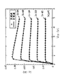
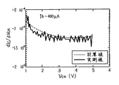
図10を参照して、エミッタ接地のGaAs HBTの特性を説明する。ベース電流Ibが一定の場合に、エミッタ−コレクタ電圧Vceの増加とともに、コレクタ電流Icの低下、すなわち電流利得の低下が観測される。またコレクタ電流Icが大きいほど電流利得の低下が顕著になる。したがって高周波パワー素子であるGaAs HBTのシミュレーションにおいては、電流利得の低下を表現するため、自己発熱効果を取り入れた等価回路モデルを使用することが不可欠である。
【0006】
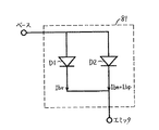
以下従来のHBT等価回路モデルについて説明する。図11および図12を参照して、HBT等価回路モデル80は、ダイオードモデル部81を含む。ダイオードモデル部81は、ダイオードモデルD1とダイオードモデルD2とを含む。従来のダイオードモデル部81においては、ダイオードモデルD1は再結合電流Ibrを表わし、ダイオードモデルD2は電子注入電流Ibnとホール注入電流Ibpとの和、すなわちIbn+Ibpを表わす。
【0007】
以下、自己発熱効果による利得低下のメカニズムについて説明する。npn型のHBTにおいて、ベース電流Ibは、
Ib=Ibr+Ibn+Ibp (1)
で表わされる。ただし、
Ibr:エミッタ接合の空乏層中の再結合電流
Ibn:エミッタからベースへの電子注入電流
Ibp:ベースからエミッタへのホール注入電流
である。
【0008】
「Procedings of IEEE、1982年1月、第70巻第1号、13頁〜25頁」に開示されているように、電子注入電流Ibnとホール注入電流Ibpとはそれぞれ下記の式(2)と式(3)で表わされる。
【0009】
Ibn=Ne・vnb・exp(qVn/kT)/β0 (2)
Ibp=Pb・vpe・exp(−qVp/kT) (3)
ここで、
β0:ベース輸送効率によるエミッタ接地電流利得
Ne:エミッタ中のドーピングレベル
Pb:ベース中のドーピングレベル
vnb:ベース中の電子の平均速度
vpe:エミッタ中のホールの平均速度
である。
【0010】
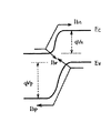
図13を参照して、エミッタに広い禁制帯幅の半導体を用い、ベースに狭い禁制帯幅の半導体を用いるHBTの場合に、エミッタ接合のエネルギバンド構造を示す。図13からわかるように、エミッタからベースへの電子に対する障壁qVnに比べて、ベースからエミッタへのホールに対する障壁qVpが高い。さらに、式(2)、式(3)からわかるように、障壁が高いほど、温度変化による電流の変化が大きい。したがって電子注入電流とホール注入電流とが各々異なった温度特性をもっており、電子注入電流に比べてホール注入電流が温度変化の影響を受けやすい。その結果、電子電流とホール電流の割合は温度に依存することになる。
【0011】
しかし、従来のダイオードモデル部81によっては、温度変化による電子注入電流とホール注入電流の割合の変化を表現することができない。
【0012】
上記のようにガンメルプーンモデルは自己発熱効果を取り入れていないので、図10に示した電流利得の低下を表現することができない。このため従来では以下の方法により、自己発熱効果を取り入れたHBT特性のシミュレーションを行なっていた。
【0013】
たとえば「IEEE Trans. 、Microwave Theory and Techniques 、1992年3月、第40巻第3号、449 頁〜464 頁」および「IEEE Trans. 、Microwave Theory and Techniques 、1995年7月、第43巻第7号、1433頁〜1445頁」に開示されているように、ガンメルプーンモデルを構成する各々の素子に温度依存性を持たせ、その消費電力からHBTの温度上昇を計算し、その温度上昇を考慮した各素子の特性を表わすパラメータを算出し、この変化したパラメータを用いて等価回路の動作をシミュレーションする。
【0014】
【発明が解決しようとする課題】
しかしながら上記の従来の自己発熱効果を取り入れたHBT特性のシミュレーション方法においては、各素子に温度特性を持たせるために、多数の新たなパラメータが必要である。このためパラメータの個数が多いほどモデルの構築のためのパラメータの抽出に多くの労力と時間を要し、シミュレーション結果の信頼性が低下する恐れがある。さらにシミュレーションの結果を利用してデバイスの設計、製作に軌道修正をかけることも困難である。
【0015】
本発明は係る課題を解決するためになされたものであり、請求項1に記載の発明の目的は、自己発熱効果を含めたHBTの特性を精度よく表現する等価回路モデルを、少数のパラメータで作成することができるHBTの等価回路モデルの作成方法を提供することにある。
【0017】
請求項2に記載の発明の目的は、HBTのベース電流を、ベース電流中の電子注入電流を表わすダイオードモデルと、ベース電流中のホール注入電流を表わすダイオードモデルとを含むダイオードモデルで表わすHBTの等価回路モデルの作成方法を提供することにある。
【0018】
請求項3に記載の発明の目的は、請求項1に記載の発明の目的に加え、HBTのベース電流を、ベース電流中の電子注入電流を表わすダイオードモデルと、ベース電流中のホール注入電流を表わすダイオードモデルとを含むダイオードモデルで表わすHBTの等価回路モデルを、短時間で作成することのできるHBTの等価回路モデルの作成方法を提供することにある。
【0019】
請求項4に記載の発明の目的は、自己発熱効果を含めたHBTの特性を精度よくシミュレーションすることのできる回路シミュレータを提供することにある。
【0020】
【課題を解決するための手段】
請求項1に記載の発明に係るHBTの等価回路モデルの作成方法は、HBTのベース電流を、ベース電流中の電子注入電流Ibnを表わす第1のダイオードモデルと、ベース電流中のホール注入電流Ibpを表わす第2のダイオードモデルとを含むダイオードモデルで表わすことにより得られるHBTの等価回路モデルを準備するステップを含む。前記第2のダイオードモデルは以下の式で定義される。
【0021】
Ibp=C・Ibn・exp[−ΔE/k(Ta+Rth・Ic・Vce)]
ただし、
Ibn:ベース電流中の電子注入電流
Ibp:ベース電流中のホール注入電流
Ta:周囲温度
Ic:コレクタ電流
Vce:エミッタ・コレクタ電圧
C,ΔE,Rth:フィッティングパラメータ
k:ボルツマン定数
本方法はさらに、前記等価回路モデル内のパラメータをフィッティングにより定めるフィッティングステップを含む。
【0022】
請求項1に記載の発明によれば、HBTのベース電流を、ベース電流中の電子注入電流Ibnを表わす第1のダイオードモデルと、ベース電流中のホール注入電流Ibpを表わす第2のダイオードモデルとを含むダイオードモデルで表わすことにより得られるHBTの等価回路モデルが準備される。第2のダイオードモデルは所定の式で定義され、等価回路モデル内のパラメータがフィッティングにより定められる。
【0023】
したがってRth、ΔE、およびCという3個のパラメータをフィッティングで定めるだけで、HBTの等価回路モデルを作成することができる。このため少数のパラメータで自己発熱効果を取り入れたHBTの特性を精度よく表現する等価回路モデルを作成することができる。
【0025】
請求項2に記載の発明に係るHBTの等価回路モデルの作成方法は、請求項1に記載の発明の構成に加えて、前記フィッティングステップは、前記等価回路モデルの各フィッティングパラメータに初期値を設定するステップと、前記各フィッティングパラメータに与えられた値に従って前記等価回路モデルの回路シミュレーションを行なって、前記等価回路モデルの特性値を計算するシミュレーションステップと、前記回路シミュレーションにより得られた特性値と、予め準備された、実測されたHBTの特性値との相違を表わす予め定める尺度を計算するステップと、前記尺度が予め定める条件を満たすまで、各フィッティングパラメータに与えられた値を変化させながら前記シミュレーションステップと前記尺度を計算するステップとを繰返し行なうステップと、前記繰返し行なうステップの終了時に得られたフィッティングパラメータの値の組を、前記一般的な等価回路モデルに適用することにより、前記HBTの等価回路モデルを作成するステップとを含む。
【0026】
請求項2に記載の発明によれば、初期値を設定するステップで、等価回路モデルの各フィッティングパラメータに初期値を設定し、シミュレーションステップで、各フィッティングパラメータに与えられた値に従って等価回路モデルの回路シミュレーションを行なって、等価回路モデルの特性値を計算する。尺度を計算するステップにおいては、回路シミュレーションにより得られた特性値と予め準備された、実測されたHBTの特性値との相違を表わす予め定める尺度を計算する。この尺度が予め定める条件を満たすまで、各フィッティングパラメータに与えられた値を変化させながらシミュレーションステップと前記尺度を計算するステップとが繰返し実行される。繰返し行なうステップの終了時に得られたフィッティングパラメータの値の組が、一般的な等価回路モデルに適用されることにより、HBTの等価回路モデルが作成される。
【0027】
こうして計算された特性値と実測された特性値とからフィッティングされたパラメータの値が、一般的な等価回路に適用されてあるHBTの等価回路モデルが作成される。このためHBTのベース電流をベース電流中の電子注入電流を表わすダイオードモデルと、ベース電流中のホール注入電流を表わすダイオードモデルとを含むダイオードモデルで表わすHBTの一般的な等価回路モデルから特定のHBTに適合したHBTの等価回路モデルを作成することができる。
【0028】
請求項3に記載の発明は、請求項1に記載の発明であって、前記初期値を設定するステップにおいて、前記パラメータCに対して、C=β0(Ne/Pb)(vnb/vpe)
ただし、Ne:エミッタ中のドーピングレベルPb:ベース中のドーピングレベルvnb:ベース中の電子の平均速度vpe:エミッタ中のホールの平均速度β0:ベース輸送効率によるエミッタ接地電流利得なる式を適用することにより得られる値が初期値として設定されることを特徴とする。
【0029】
請求項3に記載の発明によれば、初期値を設定するステップは、パラメータCに対して、上式を適用することにより得られる値を初期値として設定する。
【0030】
したがってHBTのメカニズムに密着し、明確な物理的意味を持ち、かつその値が既に知られているか、少なくともオーダー程度は知られているパラメータから算出されたフィッティングパラメータCの値が初期値として与えられる。このため繰返しステップは実測された特性値に近い特性値を初期値として開始される。この結果尺度が予め定める条件を満たすまで、繰返し回数が少なくなり、短時間でHBTの等価回路モデルを作成することができる。また正しい収束値ではない局所的な収束値に収束する恐れも少なくなる。
【0031】
請求項4に記載の発明は、ヘテロ接合バイポーラトランジスタの等価回路モデルを用いる回路シミュレータにおいて、前記等価回路は、ヘテロ接合バイポーラトランジスタのベース電流を、ベース電流中の電子注入電流Ibnを表わす第1のダイオードモデルと、ベース電流中のホール注入電流Ibpを表わす第2のダイオードモデルとを含むダイオードモデルで表わすことにより得られる等価回路モデルである。
【0032】
前記第2のダイオードモデルは、
Ibp=C・Ibn・exp[−ΔE/k(Ta+Rth・Ic・Vce)]
ただし、
Ibn:ベース電流中の電子注入電流
Ibp:ベース電流中のホール注入電流
Ta:周囲温度Ic:コレクタ電流
Vce:エミッタ・コレクタ電圧
C,ΔE,Rth:フィッティングパラメータ
k:ボルツマン定数、という前記ホール注入電流Ibpの式で表される。
【0033】
請求項4に記載の発明によれば、HBTのベース電流を、ベース電流中の電子注入電流Ibnを表わす第1のダイオードモデルと、ベース電流中のホール注入電流Ibpを表わす第2のダイオードモデルとを含むダイオードモデルで表わすことにより得られるHBTの等価回路モデルが準備される。第2のダイオードモデルは自己発熱を精度よく、かつ少ないパラメータしか用いない所定の式で定義される。等価回路モデル内のパラメータがフィッティングにより定められ、HBTの等価回路が作成される。さらに、シミュレーション対象の回路の等価回路は回路シミュレータを用いてシミュレーションされる。
【0034】
ベース電流中の電子注入電流Ibnを表わす第1のダイオードモデルと、ベース電流中のホール注入電流Ibpを表わす第2のダイオードモデルとを含むダイオードモデルで表わすことにより得られるHBTの等価回路モデルでは、自己発熱の影響がより精度よく表わされ、かつ少ないパラメータしか必要としない。パラメータは効率よく抽出でき、そのパラメータを用いて作成された等価回路を含む回路が回路シミュレータでシミュレーションされる。このため自己発熱効果を取り入れたHBTを含む回路の特性を精度よくシミュレーションすることができる。
【0038】
【発明の実施の形態】
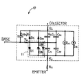
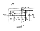
以下本願発明の実施の形態を図面を参照して説明する。図1および図2を参照して、HBT等価回路モデル10はダイオードモデル部11を含む。ダイオードモデル部11は、ダイオードモデルD1とダイオードモデルD2AとダイオードモデルD2Bとを含む。本実施の形態のHBT等価回路モデル10の特徴は、ダイオードモデル部11において、ベース電流Ibのうち、ダイオードモデルD1が再結合電流Ibrを表わし、ダイオードモデルD2Aが電子注入電流Ibnを表わし、ダイオードモデルD2Bがホール注入電流Ibpを表わすことにある。
【0039】
ダイオードモデルD2Bで表わされたホール注入電流Ibpは下記の式により定義される。
【0040】
Ibp=C・Ibn・exp[−ΔE/k(Ta+Rth・Ic・Vce)]
ただし、
Ibn:ベース電流中の電子注入電流
Ibp:ベース電流中のホール注入電流
Ta:周囲温度
Ic:コレクタ電流
Vce:エミッタ・コレクタ電圧
Rth:熱抵抗
ΔE:エミッタ接合界面におけるホール注入電流に対する障壁と電子注入電流に対する障壁との差
C:ΔE=0の場合のベース電流中のホール注入電流と電子注入電流との比
k:ボルツマン定数
上記値のうち、Rth,C,ΔEはフィッティングパラメータである。
【0041】
またフィッティングパラメータCは下記の式のように定義される。
C=β0(Ne/Pb)(vnb/vpe)
ただし、
Ne:エミッタ中のドーピングレベル
Pb:ベース中のドーピングレベル
vnb:ベース中の電子の平均速度
vpe:エミッタ中のホールの平均速度
β0:ベース輸送効率によるエミッタ接地電流利得
これら値のうち、Ne,Pb,β0の値は予め知ることができる。また、vnb/vpeの正確な値はわからないが、そのオーダー程度であれば予め知ることができる。
【0042】
このように、2つの異なった温度特性を有するダイオードモデルD2Aと、ダイオードモデルD2Bとを用いることにより、電子注入電流Ibnとホール注入電流Ibpとの割合による温度の依存特性を表現することができる。その結果、ガンメルプーンモデルをベースに、3つのパラメータC、ΔE、およびRthを新たに導入するのみで、精度よく電流利得の低下を表現することができる。また導入された3つのパラメータΔE、Rth、およびCは物理的な意味を持っている。したがってパラメータフィッティングにより、ΔE、Rth、およびCの値を抽出することにより、デバイス設計に対してフィードバックをかけることもできる。
【0043】
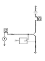
図3を参照して、回路シミュレータを用いて構築された本実施の形態の等価回路モデルについて説明する。回路シミュレータのシンボル定義がなされたデバイスSDDを用いて、
Ibp=C・Ibn・exp[−ΔE/k(Ta+Rth・Ic・Vce)]で定義されたダイオードを構築し、さらに得られたダイオードを回路シミュレータに組込まれたガンメルプーンモデルのベース/エミッタの間に挿入するだけで、電流利得の低下を表現することができる等価回路モデルを構築することができる。
【0044】
図4を参照して、GaInP/GaAs HBTのI/V特性の測定値と本実施の形態の等価回路モデルによる計算値との比較結果について説明する。図4に示されているように、コレクタ電流Icの測定値と計算値とはよく一致している。
【0045】
図5を参照して、コレクタ電流Icの測定値と計算値との電圧に対する微分、すなわち出力コンダクタンスについて説明する。等価回路モデルを用いてパワーアンプを設計する場合においては、等価回路モデルによるコレクタ電流の表現だけではなく出力コンダクタンスの表現も重要である。図5に示されているように、出力コンダクタンスの測定値と計算値とはかなり一致している。
【0046】
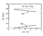
図6を参照して、ベース電流中の電子注入電流とホール注入電流の電圧依存性について説明する。HBTにおいて、トータルのベース電流Ibを測定することはできるが、ベース電流Ib中の電子注入電流Ibnとホール注入電流Ibpとを分離することは難しい。このため電子注入電流Ibnとホール注入電流Ibpとの割合はデバイスの解析にあたって重要であるにもかかわらず、それに関する測定結果はほとんど報告されていない。本実施の形態に係る等価回路モデルを用いることにより、従来分離することができなかった電子注入電流Ibnとホール注入電流Ibpとをそれぞれ計算することができる。さらに本実施の形態に係る等価回路モデルを構築する際に、HBTの回路特性の実測値から、抽出されたフィッティングパラメータC、Rth、およびΔEを本実施の形態の等価回路モデルに適用することにより、HBTを設計製作するための修正されたプロセス変数を得て、半導体デバイスの解析と開発に対してフィードバックをかけることもできる。
【0047】
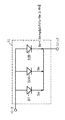
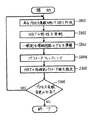
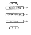
図7を参照して、本実施の形態に係るHBTの等価回路モデルを作成する方法の手順を説明する。まずガンメルプーンモデルにおいて、HBTのベース電流を、ベース電流中の電子注入電流Ibnを表わす第1のダイオードモデルと、ベース電流中のホール注入電流Ibpを表わす第2のダイオードモデルとを含むダイオードモデルで表わすことにより得られるHBTの一般的な等価回路モデルが準備される(S701)。次に等価回路モデルの各フィッティングパラメータに初期値が設定される(S702)。ここで、既に述べたようにパラメータCの初期値として、β0、Ne、Pb、vnb、vpeを用いて真の値に近いと思われる値を設定でき、以後の繰り返しにおける収束を良くすることができる。また誤った局所的最小値を解としてしまうおそれも減少する。次に各フィッティングパラメータに与えられた値に従って等価回路モデルの回路シミュレーションを行なって等価回路モデルの特性値が計算される(S703)。次に回路シミュレーションにより得られた特性値と、予め準備された、実測されたHBTの特性値との相違を表わす予め定められた尺度が計算される(S704)。この尺度の計算としては、たとえば実測値と計算値との差の最小二乗法などが用いられる。次に計算された尺度が予め定められた条件を満たすか否かが判断される(S705)。
【0048】
計算された尺度が予め定められた条件を満たしていないと判断された場合には、各フィッティングパラメータに与えられた値が変更される(S706)。次に特性値を計算するシミュレーションステップ(S703)と実測値との相違を表わす尺度を計算するステップ(S704)が繰返し実行される。
【0049】
一方計算された尺度が予め定められた条件を満たしていると判断された場合には、得られたフィッティングパラメータの値の組が、一般的な等価回路モデルに適用される。これにより特定のHBTの等価回路モデルが作成される(S707)。次に本手順は終了する。
【0050】
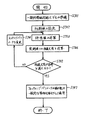
図8を参照して、本実施の形態に係るHBTの開発方法の手順について説明する。まず予め与えられた物理的パラメータを実現すべく定められたプロセス変数を用いてHBTが作成される(S801)。次に作成されたHBTの回路特性が測定される(S802)。次にガンメルプーンモデルにおいて、HBTのベース電流を、ベース電流中のベース注入電流Ibnを表わす第1のダイオードモデルと、ベース電流中のホール注入電流Ibpを表わす第2のダイオードモデルとを含むダイオードモデルで表わす変更を行なうことにより得られるHBTの一般的な等価回路モデルが準備される(S803)。次に等価回路モデル内のパラメータが、HBTの回路特性の測定値を用いたフィッティングにより定められる(S804)。次にフィッティングにより決定されたパラメータの値から、HBTの物理的パラメータの値が推定される(S805)。次に、推定された物理的パラメータの値に基づいて、プロセス変数のうちの少なくとも1つの値を変化させるべきか否かの判定が行なわれる(S806)。
【0051】
プロセス変数のうちの少なくとも1つの値を変化させるべきであると判定された場合には、推定されたパラメータに基づいて変化させたプロセス変数を用いて、再度HBTが作成され、以上の手順が再度繰り返される(S801)。
【0052】
一方いずれのプロセス変数も変化させるべきではないと判定された場合には本手順は終了する。
【0053】
なお図7で説明したHBTの等価回路モデルを作成する方法の手順は、図8のHBTの開発方法の手順においては、一般的な等価回路モデルを準備するステップ(S803)、およびパラメータフィッティングのステップ(S804)に相当する。
【0054】
図9を参照して、本実施の形態に係るHBTを含む回路のシミュレーション方法の手順について説明する。まずシミュレーション対象の回路の等価回路が準備される(S901)。次にこの等価回路内のHBTを含む等価回路モデルのパラメータをパラメータフィッティングにより定めることにより特定のシミュレーション対象の回路の等価回路が作成される(S902)。次にシミュレーション対象の回路の等価回路が回路シミュレータによりシミュレーションされる(S903)。次に本手順は終了する。
【0055】
なお図7で説明した、HBTの等価回路モデルを作成する方法の手順は、図9のHBTを含む回路のシミュレーション方法においては、等価回路モデルを作成するステップ(S902)に該当する。
【0056】
以上のように本実施の形態によれば、HBTのベース電流中の電子注入電流とホール注入電流との異なる温度依存性に注目し、異なる温度特性を持つ2つのダイオードモデルを用いて電子注入電流とホール注入電流を各々表わすこととしている。したがって熱抵抗Rth、エミッタ接合界面におけるホール注入電流に対する障壁と電子注入電流に対する障壁との差ΔE、およびΔE=0の場合のベース電流中のホール注入電流と電子注入電流との比Cという、物理的な意味を持つ3個のパラメータをガンメルプーンモデルに導入するのみで、HBTの等価回路モデルを作成することができる。このため少数のパラメータで自己発熱効果を取り入れたHBTの特性を精度よく表現できる等価回路モデルを作成することができる。
【0057】
また計算された特性値と実測された特定値とからフィッティングされたパラメータの値が一般的な等価回路モデルに適用されるため、HBTのベース電流をベース電流中の電子注入電流を表わすダイオードモデルと、ベース電流中のホール注入電流を表わすダイオードモデルとを含むダイオードモデルで表わすHBTの一般的な等価回路モデルから、HBTの等価回路モデルを作成することができる。
【0058】
またHBTのメカニズムに密着し、明確な物理的意味を持つパラメータから算出されたフィッティングパラメータCの値が初期値として与えられるため、繰返しステップは実測された特性値に近い特性値が計算されるステップから開始される。この結果尺度が予め定める条件を満たすまで繰返しを行なう回数が少なくなり、短時間でHBTの等価回路モデルを作成することができる。
【0059】
さらに測定されたHBTの回路特性に基づき、等価回路モデル内のパラメータのフィッティングの結果に従って、再度HBTを作製することができる。このため効率よくHBTを開発することができる。
【0060】
またHBTのベース電流を電子注入電流とホール注入電流とで表現した一般的な等価回路モデル内のパラメータをフィッティングにより定めることができる。こうして作成された等価回路モデルが、回路シミュレータでシミュレーションされる。このため自己発熱効果を取り入れたHBTの特性を精度よくシミュレーションすることができる。
【図面の簡単な説明】
【図1】本実施の形態に係るHBT等価回路モデルの全体構成図である。
【図2】本実施の形態に係るHBT等価回路モデルの要部の説明図である。
【図3】本実施の形態に係るシミュレータを用いて構成されたHBT等価回路モデルの説明図である。
【図4】本実施の形態に係るHBTの出力電流電圧特性の測定値と等価回路モデルによる計算値とを比較するためのグラフ図である。
【図5】本実施の形態に係るGaAs HBTの出力コンダクタンスの測定値と等価回路モデルによる計算値とを比較するためのグラフ図である。
【図6】GaAs HBTのベース電流中の電子注入電流とホール注入電流との割合の電圧依存性を示すグラフ図である。
【図7】本実施の形態に係るHBTの等価回路モデルを作成する方法の手順を示すフローチャートである。
【図8】本実施の形態に係るHBTの開発方法の手順を示すフローチャートである。
【図9】本実施の形態に係るHBTを含む回路のシミュレーション方法の手順を示すフローチャートである。
【図10】GaAs HBTの出力電流電圧特性の測定値を示すグラフ図である。
【図11】従来のHBT等価回路モデルの全体構成図である。
【図12】従来のHBT等価回路モデルの要部の説明図である。
【図13】HBTのエミッタ接合のエネルギバンド構造の説明図である。
【符号の説明】
10 HBT等価回路モデル
11 ダイオードモデル部
D1、D2、D2A、D2B ダイオードモデル[0001]
BACKGROUND OF THE INVENTION
The present invention relates to a method for creating an equivalent circuit model of a semiconductor device, and more particularly to a method for creating an equivalent circuit model of a heterojunction bipolar transistor (hereinafter referred to as “HBT”) incorporating a self-heating effect.LawOf a circuit including a HBT and an HBTToRelated.
[0002]
[Prior art]
By using an equivalent circuit model that expresses the characteristics of a semiconductor device, the design of the semiconductor circuit can be started, while the trajectory correction can be applied to the development of the semiconductor device. That is, the design can be started by obtaining physical parameters necessary for semiconductor circuit design by simulation using an equivalent circuit model. On the other hand, the design of the semiconductor device can be corrected based on the parameters fitted from the actually measured values of the already designed and manufactured characteristics and the calculated values of the simulation, and the device can be manufactured again.
[0003]
As an equivalent circuit model of HBT, as disclosed in JP-A-6-266789, the Gummel Poon model is widely used. The Gummel Poon model includes a large number of parameters indicating values of various elements (resistance, capacitance) forming an equivalent circuit of the HBT, and is formed by them.
[0004]
While GaAs HBT is being researched and developed as a high-frequency power device, the GaAs substrate has a high thermal resistance. For this reason, the influence of device self-heating on device characteristics cannot be ignored.
[0005]
With reference to FIG. 10, the characteristics of a grounded emitter GaAs HBT will be described. When the base current Ib is constant, a decrease in the collector current Ic, that is, a decrease in the current gain is observed as the emitter-collector voltage Vce increases. Moreover, the current gain decreases more significantly as the collector current Ic increases. Therefore, in the simulation of the GaAs HBT, which is a high-frequency power element, it is essential to use an equivalent circuit model that incorporates the self-heating effect in order to express a decrease in current gain.
[0006]
A conventional HBT equivalent circuit model will be described below. Referring to FIGS. 11 and 12, HBT
[0007]
Hereinafter, the mechanism of gain reduction due to the self-heating effect will be described. In the npn type HBT, the base current Ib is
Ib = Ibr + Ibn + Ibp (1)
It is represented by However,
Ibr: recombination current in the depletion layer of the emitter junction
Ibn: Electron injection current from emitter to base
Ibp: hole injection current from base to emitter
It is.
[0008]
As disclosed in “Procedings of IEEE, January 1982, Vol. 70, No. 1, pp. 13-25”, the electron injection current Ibn and the hole injection current Ibp are expressed by the following equation (2): It is represented by Formula (3).
[0009]
Ibn = Ne · vnb · exp (qVn / kT) / β0 (2)
Ibp = Pb · vpe · exp (−qVp / kT) (3)
here,
β0: Grounded emitter current gain due to base transport efficiency
Ne: doping level in the emitter
Pb: doping level in the base
vnb: average velocity of electrons in the base
vpe: average velocity of holes in the emitter
It is.
[0010]
Referring to FIG. 13, the energy band structure of the emitter junction is shown in the case of an HBT that uses a semiconductor with a wide forbidden band width as the emitter and a semiconductor with a narrow forbidden band width as the base. As can be seen from FIG. 13, the barrier qVp for holes from the base to the emitter is higher than the barrier qVn for electrons from the emitter to the base. Furthermore, as can be seen from the equations (2) and (3), the higher the barrier, the larger the change in current due to temperature change. Therefore, the electron injection current and the hole injection current have different temperature characteristics, and the hole injection current is more susceptible to temperature changes than the electron injection current. As a result, the ratio between the electron current and the hole current depends on the temperature.
[0011]
However, the conventional
[0012]
As described above, the Gummel Poon model does not incorporate the self-heating effect, and thus cannot represent the decrease in current gain shown in FIG. For this reason, conventionally, simulation of HBT characteristics incorporating the self-heating effect has been performed by the following method.
[0013]
For example, “IEEE Trans., Microwave Theory and Techniques, March 1992, Vol. 40, No. 3, pages 449-464” and “IEEE Trans., Microwave Theory and Techniques, July 1995, Vol. 43, Vol. 7 No., pp. 1433 to 1445 ”, each element constituting the Gummel Poon model has temperature dependency, and the temperature rise of the HBT is calculated from the power consumption, and the temperature rise is calculated. A parameter representing the characteristics of each element considered is calculated, and the operation of the equivalent circuit is simulated using the changed parameter.
[0014]
[Problems to be solved by the invention]
However, in the conventional HBT characteristic simulation method incorporating the above-described self-heating effect, a large number of new parameters are required to give each element temperature characteristics. For this reason, the larger the number of parameters, the more labor and time are required for extracting parameters for constructing the model, and the reliability of the simulation results may be reduced. In addition, it is difficult to make trajectory corrections for device design and production using the simulation results.
[0015]
SUMMARY OF THE INVENTION The present invention has been made to solve such problems, and an object of the present invention is to provide an equivalent circuit model that accurately expresses the characteristics of the HBT including the self-heating effect with a small number of parameters. An object of the present invention is to provide a method for creating an equivalent circuit model of an HBT that can be created.
[0017]
Claim2An object of the present invention is to provide an equivalent circuit model of an HBT in which the base current of the HBT is represented by a diode model including a diode model representing an electron injection current in the base current and a diode model representing a hole injection current in the base current. It is to provide a creation method.
[0018]
Claim3In addition to the object of the invention described in
[0019]
Claim4It is an object of the present invention to provide a circuit simulator capable of accurately simulating the characteristics of the HBT including the self-heating effect.
[0020]
[Means for Solving the Problems]
A method for creating an equivalent circuit model of an HBT according to claim 1Is HHBT obtained by representing the base current of BT with a diode model including a first diode model representing electron injection current Ibn in the base current and a second diode model representing hole injection current Ibp in the base current.Etc.Providing a valence circuit model. The second diode model is defined by the following equation.
[0021]
Ibp = C · Ibn · exp [−ΔE / k (Ta + Rth · Ic · Vce)]
However,
Ibn: electron injection current in the base current
Ibp: hole injection current in the base current
Ta: Ambient temperature
Ic: Collector current
Vce: Emitter-collector voltage
C, ΔE, Rth: Fitting parameters
k: Boltzmann constant
The method further includes a fitting step of defining parameters in the equivalent circuit model by fitting.
[0022]
According to the invention of claim 1HHBT obtained by representing the base current of BT with a diode model including a first diode model representing electron injection current Ibn in the base current and a second diode model representing hole injection current Ibp in the base current.Etc.A valence circuit model is prepared. The second diode model is defined by a predetermined formula, and parameters in the equivalent circuit model are determined by fitting.
[0023]
Therefore, an HBT equivalent circuit model can be created simply by determining three parameters Rth, ΔE, and C by fitting. Therefore, it is possible to create an equivalent circuit model that accurately expresses the characteristics of the HBT incorporating the self-heating effect with a small number of parameters.
[0025]
Claim2In addition to the configuration of the invention described in
[0026]
Claim2According to the invention, the initial value is set to each fitting parameter of the equivalent circuit model in the step of setting the initial value, and the circuit simulation of the equivalent circuit model is performed in accordance with the value given to each fitting parameter in the simulation step. Then, the characteristic value of the equivalent circuit model is calculated. In the step of calculating the scale, a predetermined scale representing the difference between the characteristic value obtained by the circuit simulation and the characteristic value of the actually measured HBT prepared in advance is calculated. Until the scale satisfies a predetermined condition, the simulation step and the step of calculating the scale are repeatedly executed while changing the value given to each fitting parameter. A set of fitting parameter values obtained at the end of the repetitive step is applied to a general equivalent circuit model, thereby creating an equivalent circuit model of the HBT.
[0027]
An HBT equivalent circuit model in which a parameter value fitted from the calculated characteristic value and the actually measured characteristic value is applied to a general equivalent circuit is created. For this reason, a specific HBT is derived from a general equivalent circuit model of the HBT in which the base current of the HBT is represented by a diode model that includes an electron injection current in the base current and a diode model that represents a hole injection current in the base current. Equivalent circuit model of HBT conforming to can be created.
[0028]
Claim3The invention according to
However, Ne: doping level in emitter Pb: doping level in base vnb: average velocity of electrons in base vpe: average velocity of holes in emitter β0: grounded emitter current gain by base transport efficiency The value obtained by the above is set as an initial value.
[0029]
Claim3According to the invention described in (1), in the step of setting the initial value, a value obtained by applying the above equation to the parameter C is set as the initial value.
[0030]
Therefore, the value of the fitting parameter C, which is closely related to the mechanism of the HBT, has a clear physical meaning, and whose value is already known or is calculated from a parameter whose order is known at least, is given as an initial value. . For this reason, the repetition step is started with a characteristic value close to the actually measured characteristic value as an initial value. As a result, the number of iterations is reduced until the scale satisfies a predetermined condition, and an equivalent circuit model of HBT can be created in a short time. In addition, there is less risk of convergence to local convergence values that are not correct convergence values..
[0031]
Claim4In the circuit simulator using the equivalent circuit model of the heterojunction bipolar transistor, the equivalent circuit includes a first diode model that represents the base current of the heterojunction bipolar transistor and the electron injection current Ibn in the base current. This is an equivalent circuit model obtained by representing a diode model including a second diode model representing the hole injection current Ibp in the base current.
[0032]
The second diode model is:
Ibp = C · Ibn · exp [−ΔE / k (Ta + Rth · Ic · Vce)]
However,
Ibn: electron injection current in the base current
Ibp: hole injection current in the base current
Ta: Ambient temperature Ic: Collector current
Vce: Emitter-collector voltage
C, ΔE, Rth: Fitting parameters
k: Boltzmann constant expressed by the formula of the hole injection current Ibp..
[0033]
Claim4According to the invention described in the above, the diode including the base current of the HBT, the first diode model representing the electron injection current Ibn in the base current, and the second diode model representing the hole injection current Ibp in the base current. An equivalent circuit model of the HBT obtained by expressing the model is prepared. The second diode model is defined by a predetermined formula that uses self-heating accurately and uses few parameters. Parameters in the equivalent circuit model are determined by fitting, and an equivalent circuit of the HBT is created. Furthermore, an equivalent circuit of the circuit to be simulated is simulated using a circuit simulator.
[0034]
In an equivalent circuit model of the HBT obtained by representing a diode model including a first diode model representing the electron injection current Ibn in the base current and a second diode model representing the hole injection current Ibp in the base current, The effect of self-heating is expressed more accurately and requires fewer parameters. A parameter can be extracted efficiently, and a circuit including an equivalent circuit created using the parameter is simulated by a circuit simulator. Therefore, it is possible to accurately simulate the characteristics of the circuit including the HBT that incorporates the self-heating effect..
[0038]
DETAILED DESCRIPTION OF THE INVENTION
Embodiments of the present invention will be described below with reference to the drawings. Referring to FIGS. 1 and 2, HBT
[0039]
The hole injection current Ibp represented by the diode model D2B is defined by the following equation.
[0040]
Ibp = C · Ibn · exp [−ΔE / k (Ta + Rth · Ic · Vce)]
However,
Ibn: electron injection current in the base current
Ibp: hole injection current in the base current
Ta: Ambient temperature
Ic: Collector current
Vce: Emitter-collector voltage
Rth: Thermal resistance
ΔE: difference between the barrier for hole injection current and the barrier for electron injection current at the emitter junction interface
C: Ratio of the hole injection current and the electron injection current in the base current when ΔE = 0
k: Boltzmann constant
Of the above values, Rth, C, and ΔE are fitting parameters.
[0041]
The fitting parameter C is defined as the following equation.
C = β0 (Ne / Pb) (vnb / vpe)
However,
Ne: doping level in the emitter
Pb: doping level in the base
vnb: average velocity of electrons in the base
vpe: average velocity of holes in the emitter
β0: Grounded emitter current gain due to base transport efficiency
Among these values, the values of Ne, Pb, and β0 can be known in advance. Moreover, although the exact value of vnb / vpe is not known, it can be known in advance if it is about the order.
[0042]
In this way, by using the diode model D2A and the diode model D2B having two different temperature characteristics, it is possible to express the temperature dependence characteristics depending on the ratio of the electron injection current Ibn and the hole injection current Ibp. As a result, it is possible to accurately represent a decrease in current gain only by newly introducing three parameters C, ΔE, and Rth based on the Gummel Poon model. The three introduced parameters ΔE, Rth, and C have physical meanings. Therefore, it is possible to apply feedback to the device design by extracting the values of ΔE, Rth, and C by parameter fitting.
[0043]
With reference to FIG. 3, an equivalent circuit model of the present embodiment constructed using a circuit simulator will be described. Using the device SDD with the symbol definition of the circuit simulator,
A diode defined by Ibp = C · Ibn · exp [−ΔE / k (Ta + Rth · Ic · Vce)] is constructed, and further, the obtained diode is incorporated into a circuit simulator of the base / emitter of the Gummel Poon model. It is possible to construct an equivalent circuit model that can express a decrease in current gain simply by inserting it in between.
[0044]
With reference to FIG. 4, the comparison result of the measured value of the I / V characteristic of GaInP / GaAs HBT and the calculated value by the equivalent circuit model of the present embodiment will be described. As shown in FIG. 4, the measured value and the calculated value of the collector current Ic are in good agreement.
[0045]
With reference to FIG. 5, the differential of the measured value and the calculated value of the collector current Ic with respect to the voltage, that is, the output conductance will be described. In designing a power amplifier using an equivalent circuit model, not only the expression of the collector current by the equivalent circuit model but also the expression of the output conductance is important. As shown in FIG. 5, the measured output conductance and the calculated value are in good agreement.
[0046]
The voltage dependence of the electron injection current and the hole injection current in the base current will be described with reference to FIG. In the HBT, the total base current Ib can be measured, but it is difficult to separate the electron injection current Ibn and the hole injection current Ibp in the base current Ib. For this reason, although the ratio between the electron injection current Ibn and the hole injection current Ibp is important in the device analysis, few measurement results have been reported. By using the equivalent circuit model according to the present embodiment, it is possible to calculate the electron injection current Ibn and the hole injection current Ibp that could not be separated conventionally. Furthermore, when the equivalent circuit model according to the present embodiment is constructed, the fitting parameters C, Rth, and ΔE extracted from the measured values of the circuit characteristics of the HBT are applied to the equivalent circuit model of the present embodiment. It is also possible to obtain modified process variables for designing and manufacturing HBTs and to provide feedback on the analysis and development of semiconductor devices.
[0047]
With reference to FIG. 7, a procedure of a method for creating an equivalent circuit model of the HBT according to the present embodiment will be described. First, in the Gummel Poon model, a diode model including a base current of the HBT, a first diode model representing an electron injection current Ibn in the base current, and a second diode model representing a hole injection current Ibp in the base current. A general equivalent circuit model of the HBT obtained by expressing is prepared (S701). Next, initial values are set for the fitting parameters of the equivalent circuit model (S702). Here, as described above, the initial value of the parameter C can be set to a value that seems to be close to the true value by using β0, Ne, Pb, vnb, vpe, and the convergence in the subsequent iterations can be improved. it can. In addition, the risk of using an incorrect local minimum as a solution is reduced. Next, a circuit simulation of the equivalent circuit model is performed according to the value given to each fitting parameter, and the characteristic value of the equivalent circuit model is calculated (S703). Next, a predetermined scale representing the difference between the characteristic value obtained by the circuit simulation and the actually measured characteristic value of the HBT prepared in advance is calculated (S704). As the calculation of this scale, for example, the least square method of the difference between the actually measured value and the calculated value is used. Next, it is determined whether or not the calculated scale satisfies a predetermined condition (S705).
[0048]
When it is determined that the calculated scale does not satisfy a predetermined condition, the value given to each fitting parameter is changed (S706). Next, a simulation step (S703) for calculating the characteristic value and a step (S704) for calculating a scale representing the difference between the actual measurement values are repeatedly executed.
[0049]
On the other hand, when it is determined that the calculated scale satisfies a predetermined condition, the obtained set of fitting parameter values is applied to a general equivalent circuit model. Thereby, an equivalent circuit model of a specific HBT is created (S707). Next, this procedure ends.
[0050]
With reference to FIG. 8, the procedure of the HBT development method according to the present embodiment will be described. First, an HBT is created using a process variable determined to realize a predetermined physical parameter (S801). Next, the circuit characteristics of the created HBT are measured (S802). Next, in the Gummel Poon model, a diode including an HBT base current, a first diode model representing a base injection current Ibn in the base current, and a second diode model representing a hole injection current Ibp in the base current A general equivalent circuit model of the HBT obtained by performing the change represented by the model is prepared (S803). Next, the parameters in the equivalent circuit model are determined by fitting using the measured values of the circuit characteristics of the HBT (S804). Next, the value of the physical parameter of the HBT is estimated from the value of the parameter determined by the fitting (S805). Next, it is determined whether or not at least one of the process variables should be changed based on the estimated value of the physical parameter (S806).
[0051]
If it is determined that the value of at least one of the process variables should be changed, the HBT is generated again using the process variable changed based on the estimated parameter, and the above procedure is performed again. Repeated (S801).
[0052]
On the other hand, if it is determined that none of the process variables should be changed, the procedure ends.
[0053]
Note that the procedure of the method of creating the equivalent circuit model of the HBT described in FIG. 7 is the step of preparing a general equivalent circuit model (S803) and the step of parameter fitting in the procedure of the development method of the HBT of FIG. This corresponds to (S804).
[0054]
With reference to FIG. 9, the procedure of the simulation method of the circuit including the HBT according to the present embodiment will be described. First, an equivalent circuit of a circuit to be simulated is prepared (S901). Next, an equivalent circuit of a specific simulation target circuit is created by determining parameters of the equivalent circuit model including the HBT in the equivalent circuit by parameter fitting (S902). Next, an equivalent circuit of the circuit to be simulated is simulated by the circuit simulator (S903). Next, this procedure ends.
[0055]
The procedure of the method for creating the equivalent circuit model of the HBT described in FIG. 7 corresponds to the step of creating an equivalent circuit model (S902) in the simulation method for the circuit including the HBT in FIG.
[0056]
As described above, according to the present embodiment, attention is paid to the different temperature dependence between the electron injection current and the hole injection current in the base current of the HBT, and the electron injection current is obtained using two diode models having different temperature characteristics. And the hole injection current respectively. Therefore, the physical resistance of the thermal resistance Rth, the difference ΔE between the barrier against the hole injection current and the barrier against the electron injection current at the emitter junction interface, and the ratio C between the hole injection current and the electron injection current in the base current when ΔE = 0. An HBT equivalent circuit model can be created simply by introducing three parameters having a specific meaning into the Gummel Poon model. Therefore, it is possible to create an equivalent circuit model that can accurately express the characteristics of the HBT incorporating the self-heating effect with a small number of parameters.
[0057]
In addition, since the parameter value fitted from the calculated characteristic value and the actually measured specific value is applied to a general equivalent circuit model, the base model current of the HBT is represented as an electron injection current in the base current, and An equivalent circuit model of the HBT can be created from a general equivalent circuit model of the HBT represented by a diode model including a diode model representing a hole injection current in the base current.
[0058]
Further, since the value of the fitting parameter C calculated from a parameter having a clear physical meaning is closely attached to the mechanism of the HBT is given as an initial value, the repetition step is a step in which a characteristic value close to the actually measured characteristic value is calculated. Starts from. As a result, the number of repetitions is reduced until the scale satisfies a predetermined condition, and an equivalent circuit model of HBT can be created in a short time.
[0059]
Further, based on the measured circuit characteristics of the HBT, the HBT can be produced again according to the result of the parameter fitting in the equivalent circuit model. For this reason, HBT can be developed efficiently.
[0060]
Further, parameters in a general equivalent circuit model in which the base current of the HBT is expressed by an electron injection current and a hole injection current can be determined by fitting. The equivalent circuit model created in this way is simulated by a circuit simulator. Therefore, it is possible to accurately simulate the characteristics of the HBT that incorporates the self-heating effect.
[Brief description of the drawings]
FIG. 1 is an overall configuration diagram of an HBT equivalent circuit model according to the present embodiment.
FIG. 2 is an explanatory diagram of a main part of an HBT equivalent circuit model according to the present embodiment.
FIG. 3 is an explanatory diagram of an HBT equivalent circuit model configured using a simulator according to the present embodiment.
FIG. 4 is a graph for comparing the measured value of the output current voltage characteristic of the HBT according to the present embodiment and the calculated value by the equivalent circuit model.
FIG. 5 is a graph for comparing the measured value of the output conductance of the GaAs HBT according to the present embodiment with the calculated value based on the equivalent circuit model.
FIG. 6 is a graph showing the voltage dependence of the ratio between the electron injection current and the hole injection current in the base current of GaAs HBT.
FIG. 7 is a flowchart showing a procedure of a method for creating an equivalent circuit model of an HBT according to the present embodiment.
FIG. 8 is a flowchart showing a procedure of an HBT development method according to the present embodiment.
FIG. 9 is a flowchart showing a procedure of a simulation method for a circuit including an HBT according to the present embodiment.
FIG. 10 is a graph showing measured values of output current voltage characteristics of GaAs HBT.
FIG. 11 is an overall configuration diagram of a conventional HBT equivalent circuit model.
FIG. 12 is an explanatory diagram of a main part of a conventional HBT equivalent circuit model.
FIG. 13 is an explanatory diagram of an energy band structure of an emitter junction of an HBT.
[Explanation of symbols]
10 HBT equivalent circuit model
11 Diode model part
D1, D2, D2A, D2B Diode model
Claims (4)
ヘテロ接合バイポーラトランジスタのベース電流を、ベース電流中の電子注入電流Ibnを表わす第1のダイオードモデルと、ベース電流中のホール注入電流Ibpを表わす第2のダイオードモデルとを含むダイオードモデルで表わすことにより得られるヘテロ接合バイポーラトランジスタの等価回路モデルを準備するステップを備え、
前記第2のダイオードモデルは以下の式で定義され、
Ibp=C・Ibn・exp[−ΔE/k(Ta+Rth・Ic・Vce)]
ただし、Ibn:ベース電流中の電子注入電流
Ibp:ベース電流中のホール注入電流
Ta:周囲温度
Ic:コレクタ電流
Vce:エミッタ・コレクタ電圧
C,ΔE,Rth:フィッティングパラメータ
k:ボルツマン定数
前記等価回路モデル内のパラメータをフィッティングにより定めるフィッティングステップをさらに備える、ヘテロ接合バイポーラトランジスタの等価回路モデルの作成方法。In a method for creating an equivalent circuit model of a heterojunction bipolar transistor,
By representing the base current of the heterojunction bipolar transistor by a diode model including a first diode model representing an electron injection current Ibn in the base current and a second diode model representing a hole injection current Ibp in the base current. Providing an equivalent circuit model of the resulting heterojunction bipolar transistor,
The second diode model is defined by the following equation:
Ibp = C · Ibn · exp [−ΔE / k (Ta + Rth · Ic · Vce)]
Where Ibn: electron injection current in the base current
Ibp: hole injection current in the base current
Ta: Ambient temperature
Ic: Collector current
Vce: Emitter-collector voltage
C, ΔE, Rth: Fitting parameters
k: Boltzmann constant A method for creating an equivalent circuit model of a heterojunction bipolar transistor, further comprising a fitting step of determining parameters in the equivalent circuit model by fitting.
前記等価回路モデルの各フィッティングパラメータに初期値を設定するステップと、
前記各フィッティングパラメータに与えられた値に従って前記等価回路モデルの回路シミュレーションを行なって、前記等価回路モデルの特性値を計算するシミュレーションステップと、
前記回路シミュレーションにより得られた特性値と、予め準備された、実測されたHBTの特性値との相違を表わす予め定める尺度を計算するステップと、
前記尺度が予め定める条件を満たすまで、各フィッティングパラメータに与えられた値を変化させながら前記シミュレーションステップと前記尺度を計算するステップとを繰返し行なうステップと、
前記繰返し行なうステップの終了時に得られたフィッティングパラメータの値の組を、前記等価回路モデルに適用することにより、前記ヘテロ接合バイポーラトランジスタの等価回路モデルを作成するステップとを含む、請求項1に記載のヘテロ接合バイポーラトランジスタの等価回路モデルの作成方法。The fitting step includes
Setting an initial value for each fitting parameter of the equivalent circuit model;
A simulation step of performing a circuit simulation of the equivalent circuit model according to a value given to each fitting parameter, and calculating a characteristic value of the equivalent circuit model;
Calculating a predetermined scale representing a difference between the characteristic value obtained by the circuit simulation and the characteristic value of the actually measured HBT prepared in advance;
Repeating the simulation step and the step of calculating the scale while changing the value given to each fitting parameter until the scale satisfies a predetermined condition;
Applying the set of fitting parameter values obtained at the end of the repetitive step to the equivalent circuit model to create an equivalent circuit model of the heterojunction bipolar transistor. To create an equivalent circuit model of a heterojunction bipolar transistor.
ただし、Ne:エミッタ中のドーピングレベル
Pb:ベース中のドーピングレベル
vnb:ベース中の電子の平均速度
vpe:エミッタ中のホールの平均速度
β0:ベース輸送効率によるエミッタ接地電流利得なる式を適用することにより得られる値が初期値として設定される、請求項1に記載のヘテロ接合バイポーラトランジスタの等価回路モデルの作成方法。In the step of setting the initial value, for the parameter C, C = β0 (Ne / Pb) (vnb / vpe)
However, Ne: doping level in emitter Pb: doping level in base vnb: average velocity of electrons in base vpe: average velocity of holes in emitter β0: grounded emitter current gain by base transport efficiency The method of creating an equivalent circuit model of a heterojunction bipolar transistor according to claim 1, wherein a value obtained by the step is set as an initial value.
前記等価回路は、ヘテロ接合バイポーラトランジスタのベース電流を、
ベース電流中の電子注入電流Ibnを表わす第1のダイオードモデルと、
ベース電流中のホール注入電流Ibpを表わす第2のダイオードモデルとを含むダイオードモデルで表わすことにより得られる等価回路モデルであり、
前記第2のダイオードモデルは、
Ibp=C・Ibn・exp[−ΔE/k(Ta+Rth・Ic・Vce)]
ただし、Ibn:ベース電流中の電子注入電流
Ibp:ベース電流中のホール注入電流
Ta:周囲温度Ic:コレクタ電流
Vce:エミッタ・コレクタ電圧
C,ΔE,Rth:フィッティングパラメータ
k:ボルツマン定数
という前記ホール注入電流Ibpの式で表されることを特徴とする、回路シミュレータ。In a circuit simulator using an equivalent circuit model of a heterojunction bipolar transistor,
The equivalent circuit calculates the base current of the heterojunction bipolar transistor,
A first diode model representing an electron injection current Ibn in the base current;
An equivalent circuit model obtained by representing a diode model including a second diode model representing a hole injection current Ibp in the base current;
The second diode model is:
Ibp = C · Ibn · exp [−ΔE / k (Ta + Rth · Ic · Vce)]
Where Ibn: electron injection current in base current Ibp: hole injection current in base current Ta: ambient temperature Ic: collector current Vce: emitter-collector voltage C, ΔE, Rth: fitting parameters k: Boltzmann constant A circuit simulator characterized by being expressed by an expression of current Ibp.
Priority Applications (1)
| Application Number | Priority Date | Filing Date | Title |
|---|---|---|---|
| JP31988796A JP3649828B2 (en) | 1996-11-29 | 1996-11-29 | Method for creating equivalent circuit model of heterojunction bipolar transistor and circuit simulator |
Applications Claiming Priority (1)
| Application Number | Priority Date | Filing Date | Title |
|---|---|---|---|
| JP31988796A JP3649828B2 (en) | 1996-11-29 | 1996-11-29 | Method for creating equivalent circuit model of heterojunction bipolar transistor and circuit simulator |
Publications (3)
| Publication Number | Publication Date |
|---|---|
| JPH10163222A JPH10163222A (en) | 1998-06-19 |
| JPH10163222A5 JPH10163222A5 (en) | 2004-11-18 |
| JP3649828B2 true JP3649828B2 (en) | 2005-05-18 |
Family
ID=18115353
Family Applications (1)
| Application Number | Title | Priority Date | Filing Date |
|---|---|---|---|
| JP31988796A Expired - Fee Related JP3649828B2 (en) | 1996-11-29 | 1996-11-29 | Method for creating equivalent circuit model of heterojunction bipolar transistor and circuit simulator |
Country Status (1)
| Country | Link |
|---|---|
| JP (1) | JP3649828B2 (en) |
Cited By (1)
| Publication number | Priority date | Publication date | Assignee | Title |
|---|---|---|---|---|
| US8745569B2 (en) | 2011-06-23 | 2014-06-03 | Panasonic Corporation | Equivalent circuit of bidirectional switch, simulation method for bidirectional switch, and simulation device for bidirectional switch |
Families Citing this family (2)
| Publication number | Priority date | Publication date | Assignee | Title |
|---|---|---|---|---|
| KR20030083889A (en) * | 2002-04-23 | 2003-11-01 | 엘지전자 주식회사 | Auto abstraction method for small-signal model of hetero junction bipolar transistor |
| CN116314174B (en) * | 2022-09-09 | 2023-11-24 | 燕山大学 | Low-temperature large-signal equivalent circuit model of germanium-silicon heterojunction bipolar transistor |
-
1996
- 1996-11-29 JP JP31988796A patent/JP3649828B2/en not_active Expired - Fee Related
Cited By (1)
| Publication number | Priority date | Publication date | Assignee | Title |
|---|---|---|---|---|
| US8745569B2 (en) | 2011-06-23 | 2014-06-03 | Panasonic Corporation | Equivalent circuit of bidirectional switch, simulation method for bidirectional switch, and simulation device for bidirectional switch |
Also Published As
| Publication number | Publication date |
|---|---|
| JPH10163222A (en) | 1998-06-19 |
Similar Documents
| Publication | Publication Date | Title |
|---|---|---|
| Rinaldi | Small-signal operation of semiconductor devices including self-heating, with application to thermal characterization and instability analysis | |
| JP3660137B2 (en) | Simulation method, simulator, recording medium recording simulation program, and method for manufacturing semiconductor device | |
| CN109800464A (en) | Method, storage medium and the computer equipment of modeling and the design of semiconductor devices | |
| Balanethiram et al. | Accurate modeling of thermal resistance for on-wafer SiGe HBTs using average thermal conductivity | |
| Schroter et al. | A computationally efficient physics-based compact bipolar transistor model for circuit design-Part I: Model formulation | |
| Huszka et al. | Extraction of compact static thermal model parameters for SiGe HBTs | |
| JP3649828B2 (en) | Method for creating equivalent circuit model of heterojunction bipolar transistor and circuit simulator | |
| CN101201850B (en) | Method for modeling SPICE model of bipolar junction transistor | |
| Jaoul et al. | Avalanche compact model featuring SiGe HBTs characteristics up to BVcbo | |
| Mazeau et al. | Behavioral thermal modeling for microwave power amplifier design | |
| JP4286924B2 (en) | SEMICONDUCTOR DEVICE MANUFACTURING METHOD, SEMICONDUCTOR DEVICE CHARACTERISTIC EVALUATION DEVICE, SEMICONDUCTOR DEVICE CHARACTERISTIC EVALUATION METHOD, AND MACHINE-READABLE RECORDING MEDIUM CONTAINING SEMICONDUCTOR DEVICE CHARACTERISTIC EVALUATION PROGRAM | |
| Sommet et al. | From 3D thermal simulation of HBT devices to their thermal model integration into circuit simulators via Ritz vectors reduction technique | |
| De Carlo et al. | Dead-space effects under near-breakdown conditions in AlGaAs/GaAs HBT's | |
| Scognamillo et al. | Improved nonlinear electrothermal simulation of bipolar transistors: Application to InP/InGaAs DHBTs | |
| JPH10163222A5 (en) | ||
| JPH08327698A (en) | Circuit simulation method and apparatus thereof | |
| JP3214108B2 (en) | Simulation method of semiconductor device | |
| Xia et al. | A new approach to implementing high-frequency correlated noise for bipolar transistor compact modeling | |
| Sommet et al. | Model order reduction of linear and nonlinear 3D thermal finite‐element description of microwave devices for circuit analysis | |
| JP2001291723A (en) | Thermal resistance analysis method and temperature analysis method of heating object | |
| Dai et al. | Simplified equivalent‐circuit modelling for decoupled and partial decoupled methods in semiconductor device simulation | |
| JP3313281B2 (en) | Method for evaluating characteristics of semiconductor device | |
| Ko et al. | A nonquasi-static table-based small-signal model of heterojunction bipolar transistor | |
| Zhu et al. | Simulating multi-finger power HBTS | |
| JP2655125B2 (en) | Device simulation method |
Legal Events
| Date | Code | Title | Description |
|---|---|---|---|
| A977 | Report on retrieval |
Free format text: JAPANESE INTERMEDIATE CODE: A971007 Effective date: 20040917 |
|
| A131 | Notification of reasons for refusal |
Free format text: JAPANESE INTERMEDIATE CODE: A131 Effective date: 20040928 |
|
| A521 | Request for written amendment filed |
Free format text: JAPANESE INTERMEDIATE CODE: A523 Effective date: 20041126 |
|
| TRDD | Decision of grant or rejection written | ||
| A01 | Written decision to grant a patent or to grant a registration (utility model) |
Free format text: JAPANESE INTERMEDIATE CODE: A01 Effective date: 20050201 |
|
| A61 | First payment of annual fees (during grant procedure) |
Free format text: JAPANESE INTERMEDIATE CODE: A61 Effective date: 20050216 |
|
| R150 | Certificate of patent or registration of utility model |
Free format text: JAPANESE INTERMEDIATE CODE: R150 |
|
| FPAY | Renewal fee payment (event date is renewal date of database) |
Free format text: PAYMENT UNTIL: 20080225 Year of fee payment: 3 |
|
| FPAY | Renewal fee payment (event date is renewal date of database) |
Free format text: PAYMENT UNTIL: 20090225 Year of fee payment: 4 |
|
| LAPS | Cancellation because of no payment of annual fees |