JP3639807B2 - Optical element and manufacturing method - Google Patents
Optical element and manufacturing method Download PDFInfo
- Publication number
- JP3639807B2 JP3639807B2 JP2001244970A JP2001244970A JP3639807B2 JP 3639807 B2 JP3639807 B2 JP 3639807B2 JP 2001244970 A JP2001244970 A JP 2001244970A JP 2001244970 A JP2001244970 A JP 2001244970A JP 3639807 B2 JP3639807 B2 JP 3639807B2
- Authority
- JP
- Japan
- Prior art keywords
- axis
- optical
- optical system
- optical element
- intrinsic birefringence
- Prior art date
- Legal status (The legal status is an assumption and is not a legal conclusion. Google has not performed a legal analysis and makes no representation as to the accuracy of the status listed.)
- Expired - Fee Related
Links
Images


Classifications
-
- G—PHYSICS
- G03—PHOTOGRAPHY; CINEMATOGRAPHY; ANALOGOUS TECHNIQUES USING WAVES OTHER THAN OPTICAL WAVES; ELECTROGRAPHY; HOLOGRAPHY
- G03F—PHOTOMECHANICAL PRODUCTION OF TEXTURED OR PATTERNED SURFACES, e.g. FOR PRINTING, FOR PROCESSING OF SEMICONDUCTOR DEVICES; MATERIALS THEREFOR; ORIGINALS THEREFOR; APPARATUS SPECIALLY ADAPTED THEREFOR
- G03F7/00—Photomechanical, e.g. photolithographic, production of textured or patterned surfaces, e.g. printing surfaces; Materials therefor, e.g. comprising photoresists; Apparatus specially adapted therefor
- G03F7/70—Microphotolithographic exposure; Apparatus therefor
- G03F7/708—Construction of apparatus, e.g. environment aspects, hygiene aspects or materials
- G03F7/7095—Materials, e.g. materials for housing, stage or other support having particular properties, e.g. weight, strength, conductivity, thermal expansion coefficient
- G03F7/70958—Optical materials or coatings, e.g. with particular transmittance, reflectance or anti-reflection properties
- G03F7/70966—Birefringence
-
- G—PHYSICS
- G02—OPTICS
- G02B—OPTICAL ELEMENTS, SYSTEMS OR APPARATUS
- G02B1/00—Optical elements characterised by the material of which they are made; Optical coatings for optical elements
-
- C—CHEMISTRY; METALLURGY
- C30—CRYSTAL GROWTH
- C30B—SINGLE-CRYSTAL GROWTH; UNIDIRECTIONAL SOLIDIFICATION OF EUTECTIC MATERIAL OR UNIDIRECTIONAL DEMIXING OF EUTECTOID MATERIAL; REFINING BY ZONE-MELTING OF MATERIAL; PRODUCTION OF A HOMOGENEOUS POLYCRYSTALLINE MATERIAL WITH DEFINED STRUCTURE; SINGLE CRYSTALS OR HOMOGENEOUS POLYCRYSTALLINE MATERIAL WITH DEFINED STRUCTURE; AFTER-TREATMENT OF SINGLE CRYSTALS OR A HOMOGENEOUS POLYCRYSTALLINE MATERIAL WITH DEFINED STRUCTURE; APPARATUS THEREFOR
- C30B11/00—Single-crystal growth by normal freezing or freezing under temperature gradient, e.g. Bridgman-Stockbarger method
-
- C—CHEMISTRY; METALLURGY
- C30—CRYSTAL GROWTH
- C30B—SINGLE-CRYSTAL GROWTH; UNIDIRECTIONAL SOLIDIFICATION OF EUTECTIC MATERIAL OR UNIDIRECTIONAL DEMIXING OF EUTECTOID MATERIAL; REFINING BY ZONE-MELTING OF MATERIAL; PRODUCTION OF A HOMOGENEOUS POLYCRYSTALLINE MATERIAL WITH DEFINED STRUCTURE; SINGLE CRYSTALS OR HOMOGENEOUS POLYCRYSTALLINE MATERIAL WITH DEFINED STRUCTURE; AFTER-TREATMENT OF SINGLE CRYSTALS OR A HOMOGENEOUS POLYCRYSTALLINE MATERIAL WITH DEFINED STRUCTURE; APPARATUS THEREFOR
- C30B29/00—Single crystals or homogeneous polycrystalline material with defined structure characterised by the material or by their shape
- C30B29/10—Inorganic compounds or compositions
- C30B29/12—Halides
-
- G—PHYSICS
- G02—OPTICS
- G02B—OPTICAL ELEMENTS, SYSTEMS OR APPARATUS
- G02B1/00—Optical elements characterised by the material of which they are made; Optical coatings for optical elements
- G02B1/02—Optical elements characterised by the material of which they are made; Optical coatings for optical elements made of crystals, e.g. rock-salt, semi-conductors
-
- Y—GENERAL TAGGING OF NEW TECHNOLOGICAL DEVELOPMENTS; GENERAL TAGGING OF CROSS-SECTIONAL TECHNOLOGIES SPANNING OVER SEVERAL SECTIONS OF THE IPC; TECHNICAL SUBJECTS COVERED BY FORMER USPC CROSS-REFERENCE ART COLLECTIONS [XRACs] AND DIGESTS
- Y10—TECHNICAL SUBJECTS COVERED BY FORMER USPC
- Y10S—TECHNICAL SUBJECTS COVERED BY FORMER USPC CROSS-REFERENCE ART COLLECTIONS [XRACs] AND DIGESTS
- Y10S117/00—Single-crystal, oriented-crystal, and epitaxy growth processes; non-coating apparatus therefor
- Y10S117/918—Single-crystal waveguide
Abstract
Description
【0001】
【発明の属する技術分野】
本発明は、一般には、光学素子に係り、特に、真空紫外域から遠紫外光までの短波長範囲において用いられる弗化カルシウム(CaF2)、弗化バリウム(BaF2)、弗化ストロンチウム(SrF2)等の等軸晶系結晶よりなる光学素子及びその製造方法に関する。
【0002】
【従来の技術】
近年の電子機器の小型及び薄型化の要請から電子機器に搭載される半導体素子の微細化への要求は益々高くなっており、かかる要求を満足するために露光解像度を高める提案が様々なされている。露光光源の波長を短くすることは解像度の向上に有効な一手段であるため、近年では、露光光源はKrFエキシマレーザー(波長約248nm)からArFエキシマレーザー(波長約193nm)になろうとしており、F2エキシマレーザー(波長約157nm)の実用化も進んでいる。弗化カルシウム単結晶(CaF2)は、かかる波長域の光の透過率(即ち、内部透過率)が高いために露光光学系に使用されるレンズや回折格子などの光学素子の光学材料として最適である。また、弗化バリウム単結晶(BaF2)や弗化ストロンチウム単結晶(SrF2)も透過率が高いため、応用が検討されている。
【0003】
弗化カルシウム単結晶は、従来から、(「ブリッジマン法」としても知られる)坩堝降下法によって製造されている。かかる方法は、結晶性物質の原料を坩堝内に充填し、ヒーターによる加熱により融解させた原料を坩堝を降下させて冷却することによって結晶化する方法である。この際、坩堝の下部に成長させたい面方位を持つ成長の起点となる種結晶を配置することによって、成長する結晶の面方位を制御している。弗化カルシウムは、一般的に、結晶方位[1 1 1]軸に垂直な<1 1 1>面の壁開面が扱い易く、更に[1 1 1]軸方向の光線に関し光弾性による複屈折の影響が少ないという長所を有する。その製造に際し弗化カルシウムは、<1 1 1>面に配向する種結晶を用いてかかる面方位に制御されて成長させる、又は、結晶の<1 1 1>面を切り出すことにより所望の光学素子に形成され、<1 1 1>面を光線入射面とする光学素子として実現されていた。これより、かかる光学素子よりなる光学系の光軸は[1 11]軸と一致され、光学素子(又は光学系)の光学特性を向上に寄与していた。
【0004】
【発明が解決しようとする課題】
しかし、弗化カルシウムは、理想的な応力歪みがない結晶が成長できたとしても、使用する波長が短くなると潜在的な複屈折(真性(intrinsic)複屈折)が無視できなくなり、かかる真性複屈折が光学素子の光学特性、ひいては露光装置の結像性能を悪化させるという問題を有する。このことは2001年5月にDana Pointにて開催された、2nd InternationalSymposium on 157nm LithographyにおいてBurnettらによって発表された。弗化カルシウムの真性複屈折の最大値は、彼らの実験値を参照するに、波長157nmで最大6.5nm/cmであり、かかる最大値を示す方向は[1 1 0]軸方向など12の方向に存在する。
【0005】
従来の露光装置、特に投影光学系において、上述した<1 1 1>面を用いる光学素子は、光軸である[1 1 1]軸と最大の複屈折を示す[1 1 0]軸が35.26°しか離れていない。例えば、弗化カルシウムにおいて[1 1 0]軸を通る光束のNAは波長193nmでは0.87、波長157nmにおいては0.90である。特に、近年の露光装置においては、解像度の向上に起因し投影光学系のNAは増大傾向にあり、かかるNAは0.65から0.80のものが主流となっている。よって、光線の最大角が最大となるウェハ側に近い投影光学系の光学素子では、[1 1 0]軸に近い真性複屈折の値が大きなところを光線が通過してしまう。これにより、従来の露光装置では結像性能よく露光することが困難となる。
【0006】
【課題を解決するための手段】
そこで、本発明は、高NAにおける真性複屈折の影響を低減可能な光学素子及び製造方法、露光装置及びデバイス製造方法を提供することを例示的目的とする。
【0007】
以下、説明は特に弗化カルシウムにおいて記載するが、同じ結晶性質を有する等軸晶系の結晶である、弗化バリウムと弗化ストロンチウムに関しても同様のことが言える。
【0008】
上記目的を達成するために、本発明の一側面としての光学素子は、等軸晶系結晶の結晶方位に関する[0 0 1]軸と光軸とのなす角度が10°未満(好ましくは0度)である。
【0009】
また、本発明の一側面としての光学素子は、等軸晶系結晶の結晶方位に関する[0 0 1]軸と、用いられる光学系の光軸とのなす角度が10°未満(好ましくは0度)である。
【0010】
かかる光学素子によれば、弗化カルシウム結晶の結晶方位に関する[0 0 1]軸と光軸とのなす角度が10°未満である。かかる光学素子によれば、真性複屈折は[0 0 1]軸から45°傾いたときに最大値となる。よって、結晶面内での光線の角度と真性複屈折に関し[1 1 1]軸に光軸を一致させた場合と[0 0 1]軸に光軸を一致させた場合とを比べると、[0 0 1]軸に光軸を一致させた方が真性複屈折のピークとなる角度を遠くすることができる。従って、<0 0 1>面の光学素子、即ち、光軸と[0 0 1]軸を一致させた光学素子100の方が、高NAに対して結像性能を悪化させない。また、[0 0 1]軸に光軸を一致させた場合、真性複屈折ピークは臨界角より外側に存在する。光学素子の出射面が平面であるときには、たとえ高NAであったとしても複屈折がピークとなることを防止している。本発明の光学素子100は、光線の光軸と[0 0 1]軸とが厳密に一致することを要求しない。しかし、光学素子100は光軸と[0 0 1]軸とのなす角度が少なくとも10°未満となるように構成される必要がある。これにより、従来の[1 1 1]軸に光軸を一致させた場合と実質的に同様な真性複屈折量と結晶内での光線の角度の関係となることを防ぐことができる。また、かかる角度は、真性複屈折のピークが臨界角内に入ることを防ぐことができる。なお、臨界角は光線の出射側の面が平面に近い場合の指標である。
【0011】
更に、本発明の別の側面としての光学素子の製造方法は、等軸晶系結晶を成長させる工程と、前記成長された等軸晶系結晶から光学素子を成形する工程とを有し、前記成長工程は、成長する結晶の面方位が<0 0 1>面となるように成長を制御する工程を有する。もしくは、等軸晶系結晶を成長させる工程と、前記成長された等軸晶系結晶から光学素子を成形する工程とを有し、前記成形ステップは、前記成長された等軸晶系結晶を<0 0 1>面に関し切り出すことを特徴とする。かかる光学素子の製造方法によれば、光線の光軸が弗化カルシウムの[0 0 1]軸と一致する光学素子を製造可能であり、光学特性に優れた光学素子を提供することができる。かかる光学素子の製造方法は、上述した光学素子の製造方法に好適である。
【0012】
更に、本発明の別の側面としての光学素子は、上述の製造方法により製造される。かかる製造方法により製造される光学素子によれば、上述の光学素子と同様な作用を奏する。なお、前記光学素子は、前記光学素子は、前記等軸晶系結晶の結晶方位に関する[0 0 1]軸と当該光学素子の光軸とのなす角度が10°未満となることが好ましい。
【0013】
以上説明した光学素子において、前記等軸晶系結晶は弗化カルシウム、弗化バリウム又は弗化ストロンチウムである。
【0014】
更に、本発明の別の側面としての投影光学系は、上述したいずれかの光学素子を有する。かかる投影光学系によれば、上述した光学素子を有し同様の作用を奏する。よって、かかる投影光学系は、結像性能の向上を達成可能である。
【0015】
更に、本発明の別の側面としての縮小投影光学系は、上述したいずれかの光学素子を像側の光学部材に有する。かかる縮小投影光学系によれば、上述した光学素子を有し同様の作用を奏すると共に、縮小投影光学系ではNAが1番大きくなるところは像側であって、かかる光学部材に本発明を使用することで、結像性能を上げることができる。
【0016】
更に、本発明の別の側面としての投影光学系は、光線と光軸のなす最大角度が光学素子内で25°以上となる光学部材が上述したいずれかの光学素子を有する。かかる投影光学系によれば、上述した光学素子を有し同様の作用を奏すると共に、25°以上、即ちNAが0.65以上の投影光学系に好適である。
【0017】
更に、本発明の別の側面としての投影光学系は、上述した光学素子を有する投影光学系において、[0 0 1]軸と垂直な[0 1 0]軸が、投影する物体のパターンの特徴的な方向に対して10°以上ずれている。かかる投影光学系によれば、物体のパターンの特徴的な方向と、光学素子における光軸周りの真性複屈折のピーク方向をずらすことが可能であり、結像性能をあげることができる。前記物体の特徴的な方向は、前記物体の一方向に関し0°、45°、又は90°である。
【0018】
更に、本発明の別の側面としての投影光学系は、上述した光学素子をn個有し、一の光学素子の[0 0 1]軸と垂直な[0 1 0]軸がそれと異なる光学素子の[0 0 1]軸と垂直な[0 1 0]軸とが互いに90/n±10°以内であるようにn個の前記光学素子を光軸回りにずらして配置する。かかる投影光学系によれば、n個以上の光学素子における光軸周りの真性複屈折のピーク方向をずらすことで、良好な結像性能を得ることができる。
【0019】
更に、本発明の別の側面としての光学系は、真性(intrinsic)複屈折を持つ光学素子を少なくとも一つ有する光学系であって、
当該光学系における複屈折をn、使用波長をλとした際に、結像に寄与する全ての光束に対し当該光学系における複屈折の大きさが n < λ/4を満たすことを特徴とする。かかる光学系によれば、等軸晶系結晶の結晶方位に関する軸と光軸の関係により光学系全体の真性複屈折の大きさをλ/4以下とするので、結像性能に優れる。かかる光学系は、前記複屈折nは応力による複屈折を有し、当該応力複屈折がほぼ0であり、前記真性複屈折がλ/4より小さい。前記複屈折nは、 n < λ/10を更に満たしてもよい。また、前記複屈折nは、n< λ/20を更に満たしてもよい。前記光学素子はそれぞれ等軸晶系結晶より成り、前記光学素子の結晶方位の軸と光軸との関係が、前記光学系における真性複屈折がλ/4以下、好ましくはλ/10以下となるように設定してある。なお、かかる光学系を有する投影光学系も本発明の一部として機能する。
【0020】
更に、本発明の別の側面としての光学系は、等軸晶系結晶の結晶方位に関する[1 1 0]軸と光軸とがなす角が10度未満である(好ましくは0度)複数の光学素子を有する光学系において、2以上の前記光学素子の前記[1 1 0]軸に直交する一の軸の相対角度が異なる。かかる光学系は、当該光学系に入射した光線に関し、光学素子で進んできた(又は、遅れてきた)偏光成分の位相を[1 1 0]軸と直交する一の軸の相対角度が異なる光学素子で遅らせる(又は、進ませる)ことにより、かかる偏光成分の位相のずれをキャンセルし真性複屈折の影響を低減することができる。前記2以上の光学素子は、当該光学素子を前記[1 1 0]軸と直交する面に関して分割した光学部材と置換可能である。前記光学系が2の前記光学素子を含む場合、当該2の光学素子の前記[1 10]軸に直交する軸の相対角度は、90°である。前記2の光学素子は、厚みが等しい平行平板又は厚みが等しいレンズである。かかる光学系の前記等軸晶系結晶はフッ化物であることを特徴とする。前記等軸晶系結晶は弗化カルシウム、弗化バリウム又は弗化ストロンチウムであることを特徴とする。
【0021】
更に、本発明の別の側面として投影光学系は、上記の[1 1 0]軸と光軸が一致した2以上の光学素子よりなる光学系を有する。更に、本発明の別の側面として縮小投影光学系は、等軸晶系結晶を光学素子として有する縮小投影光学系において、マージナル光線の角度が前記光学素子内で24.6°以上となる像側の2以上の前記光学素子に対し請求項21乃至25のうちいずれか一項記載の光学系を有する。かかる投影光学系は上述の光学系を有し、同様の作用を相する。かかる投影光学系の前記2以上の光学素子を除いた光学素子は、等軸晶系結晶の結晶方位に関する[1 1 1]軸と光軸とが成す角が10度未満である。又は、前記投影光学系の前記2以上の光学素子を除いた光学素子は、等軸晶系結晶の結晶方位に関する[0 0 1]軸と光軸とが成す角が10度未満である。または、前記投影光学系の前記2以上の光学素子を除いた光学素子は、等軸晶系結晶の結晶方位に関する[1 1 1]軸又は[0 0 1]軸と光軸とが成す角が10度未満である。また、かかる投影光学系は、上述の[0 0 1]軸の光学素子をm個有し、該m個の光学素子のうちn(<m)個の光学素子の前記[0 0 1]軸はほぼ一致しており、該個の光学素子のうちm−n個の光学素子の前記[0 0 1]軸はほぼ一致し且つ前記n個の光学素子の前記[0 0 1]軸と直交しており、前記n個の光学素子の厚み(軸上肉厚)の合計と前記m−n個の光学素子の厚みの合計の差は10mm以内である。かかる光学系において、前記投影光学系の前記2以上の光学素子を除いた光学素子の前記光軸に直交する軸の相対角度を変化させることにより真性複屈折を低減することを特徴としている。
【0022】
上述の光学系は、波長が200nm以下の光源を用いる。前記光源はArFエキシマレーザー又はF2エキシマレーザである。
【0023】
更に、本発明の別の側面としての光学素子は、レンズ、回折格子、平行平板、光学膜体及びそれらの複合体の一つである上述した光学素子又は光学系である。かかる光学素子によれば、上述した光学素子と同様の作用を奏する。
【0024】
更に、本発明の別の側面としての露光装置は、紫外光、遠紫外光及び真空紫外光を露光光として利用し、当該露光光を、上記の光学系を介して被処理体に投影して当該被処理体を露光する。かかる露光装置によれば、上述した光学素子を含み、結像性能よく露光することが可能である。
【0025】
更に、本発明の別の側面としてのデバイス製造方法は、かかる露光装置を用いて前記被処理体を投影露光するステップと、前記投影露光された前記被処理体に所定のプロセスを行うステップとを有する。かかる露光装置によれば、上述した露光装置と同様の作用を奏する。また、かかる露光装置を使用したデバイス製造方法並びに結果物としてのデバイスも本発明の一側面として機能する。
【0026】
本発明の他の目的及び更なる特徴は以下添付図面を参照して説明される好ましい実施例によって明らかにされるであろう。
【0027】
【発明の実施の形態】
本発明者らは、等軸晶系結晶の結晶方位を吟味し真性複屈折に関し鋭意検討した結果、かかる等軸晶系結晶よりなる光学素子では従来のように[1 1 1]軸と光軸を一致させる場合よりも、[0 0 1]軸と光軸を一致させる方が真性複屈折の影響を低減できることを発見した。なお、以下の説明では等軸晶系結晶として例示的に弗化カルシウム(CaF2)を用いて説明を行うが、これに限定されるものではない。同じ結晶性質を有する等軸晶系の結晶である、弗化バリウムと弗化ストロンチウムに関しても同様のことが言えるものである。
【0028】
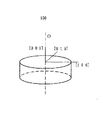
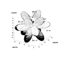
以下、図1乃至図5を参照するに、かかる理由と共に本発明の光学素子100及びかかる光学素子100を適用可能した投影光学系200について説明する。ここで、図1は、本発明の光学素子100を示す模式図である。図2は、図1に示す光学素子100を適用した投影光学系200を示す概略側面図である。図3は、波長157nmにおける弗化カルシウムの真性複屈折量とその方位を3次元的に示したシミュレーション結果である。図4は、図3に示す[0 0 1]軸及び[1 0 0]軸を通る平面内における真性複屈折量とその方位を2次元的に示したシミュレーション結果、並びに[0 0 1]軸に光軸を合わせた場合のかかる光軸と真性複屈折ピークまでの角度を示した図である。図5は、結晶面内での光線の角度と真性複屈折の関係を示した図である。図3及び図4において、原点からの距離が真性複屈折量を示している。なお、図3に示される真性複屈折は各象限において対称性を有するものであり、以下の説明では主に第1象限に関して説明を展開する。よって、その他の象限においても同様な結果となるため本明細書では重複する説明は省略する。なお、上段にて[0 0 1]軸と光軸を一致させる方が真性複屈折の影響を低減できると述べたが、上述した真性複屈折の対称性より、[0 1 0]軸、[1 0 0]軸であっても同様な[0 0 1]軸と同様な作用及び効果を奏するものである。よって、本明細書中に表現される[0 0 1]軸は、[1 0 0]軸及び[0 1 0]軸など残り5個の軸に代替可能であり、本明細書では[0 0 1]軸はこれら6つの軸を総括するものであることに理解されたい。
【0029】
図3に良く示されるように、CaF2単結晶は[1 1 1]軸における真性複屈折は小さく、かかる観点からすると[1 1 1]軸が光軸と一致するようにレンズなどの光学素子を成形することは有効である。しかし、CaF2は、例えば、[1 1 0]軸をはじめ対称的に12方向に真性複屈折がピーク(6.5nm/cm、Burnettらによる実験値)を示している。例えば、投影光学系において、近年の高NA化にともないNAは拡大傾向にある。CaF2の<1 1 1>面は、[1 1 1]軸に一致する光線に関し複屈折は非常に小さな値となるが、[1 1 1]軸から光線が傾いた場合(即ち、NAが大きくなった場合)、上述したように傾きが35.26°で真性複屈折のピークに位置してしまう。CaF2の波長157nmにおける臨界角は39.9°程度であり、高NAの光学系に適用される光学素子に[1 1 1]軸を適用したならば光線の最大角部分が真性複屈折のピーク近傍になってしまい、かかる光学素子を有する投影光学系は結像性能を悪化させてしまい好ましくない。
【0030】
そこで、図1に良く示されるように、本発明の光学素子100は結晶方位に関し[0 0 1]軸と光軸Oとを一致させることを特徴としている。[0 0 1]軸は、[1 1 1]軸と同様、かかる軸における真性複屈折の値が小さい。また、[0 0 1]軸が光軸Oとなるように構成された光学素子100では、図4に良く示されるように、真性複屈折は[0 0 1]軸から45°傾いたときに最大値となっている。そこで、図3に示すように、結晶面内での光線の角度と真性複屈折に関し[1 1 1]軸に光線の光軸を一致させた場合と[0 01]軸に光線光軸を一致させた場合とを比べるとピークまでの距離は35.26°<45°となり、[0 0 1]軸に素子(又は光学系)の光軸を一致させた方が真性複屈折のピークとなる角度が遠くなっている。従って、<0 0 1>面、即ち、光軸Oと[0 0 1]軸を一致させた光学素子100の方が、高NAに対して結像性能を悪化させないことになる。また、[1 1 1]軸に光軸を一致させた場合は、かかる真性複屈折ピークは臨界角より内側に存在するが、[0 0 1]軸に光軸を一致させた場合、真性複屈折ピークは臨界角より外側に存在する。従って、[0 0 1]軸を使用することは、高NAの光学系において複屈折がピークとなることを防止することができる。更には、NAが0.65、0.7、0.8であっても、[0 0 1]軸に光軸が一致するようにした光学素子100の方は真性複屈折が小さな値を示していることが理解される。
【0031】
なお、本発明の光学素子100において、[0 0 1]軸と光線の光軸Oを一致させるように光学素子100を製造したとしても、実際は製造誤差などにより結晶の[0 0 1]軸が光学素子100の光軸Oと完全に一致しないことがある。よって、本発明の光学素子100は、光線の光軸Oと[0 0 1]軸とが厳密に一致することを要求しない。しかし、以下に示す理由により、光学素子100は光軸Oと[0 0 1]軸とのなす角度が少なくとも10°未満となるように構成される必要がある。これは、図5より説明可能であるが、仮に光学素子100の光軸が[0 0 1]軸に対して10°傾いていた場合、かかる光学素子100に光線を光軸Oと平行となるよう光を入射させたとする。しかし実際には、かかる光学素子100に垂直に入射した光軸は、予め[0 0 1]軸と光線の光軸Oとが10°の角度差がつけられていることになる(例えば、図4の光軸が左側に10°傾いているものとする)。この場合、光学素子100は、図5に示す実線を相対的に左に10°だけずらさなければ真の真性複屈折に相当しない。このとき、実線と破線はほぼ一致し、従来の[1 1 1]軸に光線の光軸を一致させた場合と実質的に同様な真性複屈折量と結晶内での光線の角度の関係となってしまう。(なお、仮に図4の光軸が右側に10°傾いた場合は、図5に示す実線を右に10°だけずらさなければ正しい真性複屈折にならない。このとき、図5中左側に位置する真性複屈折のピークが臨界角内に入ってきてしまい、これも同様に好ましくない。)また、[0 0 1]軸と光軸Oが10°以上ずれた場合には、光軸Oと真性複屈折ピークが近い値となり、当然このましくない。そこで、本発明はかかる弊害を防止すべく、また、製造誤差を考慮して、光学素子100の[0 0 1]軸と光軸Oとのなす角度が10°以内となるように制限している。
【0032】
図2に示すように、かかる光学素子100は投影光学系200に好適であり、特に、投影光学系の倍率が縮小の場合には、投影光学系の像面P側の位置する光学部材L1に適用されることが好ましい。なお、図2に示すように、投影光学系200には4枚の光学部材L1乃至L4より構成されており、本実施形態において、像面P側から1枚目の光学部材L1に光学素子100を適用している。しかし、かかる投影光学系200の光学部材L1乃至L4の数は例示的でありこれに限定されるものでない。また、投影光学系200は、像面P側で高NAであるなら、像面P側から2枚目の光学部材L2にも光学素子100を適用しても良い。上述したように、かかる部分に位置する光学部材は光線と光軸Oのなす最大角が光学部材内で大きくなるからであり、より特定的には、かかる最大角が25°以上となる光学部材に関して光学素子100を使用することが良い。25°はNAが0.65に対応し、本発明はNA0.65以上の高NAに対して好適である。
【0033】
なお、図3、図6及び図7を参照するに、かかる光学素子100の<0 0 1>面において、光軸O回りに90°間隔に直交する2方向として真性複屈折のピークが存在している。ここで、図6は、図3にしめすシミュレーション結果を[0 0 1]軸方向から見たときの真性複屈折を示すシミュレーション結果である。図7は、光軸回りの方位角に対する真性複屈折を示した図である。なお、図14を参照するに、<1 1 1>面における光軸回りの真性複屈折は120°間隔でピークが出現する。ここで、図14は、図7に示す図に<1 1 1>面における光軸回りの方位角に対する真性複屈折を加えた図である。図に良く示されるように、光軸回りの方位角に対する真性複屈折は<1 1 1>面よりも<0 0 1>面のほうが相対的に低い値を示し、かかる点からも本発明の光学素子100は真性複屈折の影響を受けにくいことが理解できる。
【0034】
一方、図8を参照するに、投影光学系が結像する物体Mのパターンは、典型的に、0、45、90°などの特徴的な角度のパターンを多用することが多い。ここで、図8は、図2に示す投影光学系200を示す概略斜視図である。なお、図8において、投影光学系200の光学部材の一部はその図示を省略されている。このような特徴的なパターンは、例えば、物体Mの一方向(例えば、y方向)を基準に、パターンが0°、45°又は90°となるように形成されるパターン、又は、これらのパターンを複数組み合わせて成るパターンである。図8には、y方向を基準に0°となるパターンとして描かれている。投影光学系200がかかるパターンを結像する場合、真性複屈折の2方向のうちいずれか一の方向と物体Mのパターンを結像する光束の光路とが一致すると、結像性能が悪化してしまう。よって、本発明の光学素子100を有する投影光学系200は、真性複屈折のピークのうちいずれか一つとかかるパターン方向とが一致しないように10°以上ずらして光学部材L1を配置することが望ましい。
【0035】
また、投影光学系200において、2の光学部材L1及びL2に光学素子100を適用するのであれば、図9に示すように、かかる光学部材L1及びL2のうちいずれか一方の[0 0 1]軸と直交する[0 1 0]軸(又は、[1 0 0]軸)が他方の[0 1 0]軸(又は、[1 0 0]軸)が光軸周りに45°ずらして配置されていることが好ましい。ここで、図9は、図2に示す投影光学系200の例示的一態様を示した概略斜視図である。図8において、投影光学系200の光学部材の一部はその図示を省略されている。これは、2の光学素子100を有する投影光学系200では、直交する2方向として現れる真性複屈折のピークが重ならない方が、投影光学系200の光学特性を上げることができるからである。なお、投影光学系200が、光学素子100をn個有するのであれば、一の光学素子の[0 0 1]軸と垂直な[0 1 0]軸がそれと異なる光学素子の[0 0 1]軸と垂直な[0 1 0]軸とが互いに90/n±10°以内であるようにn個の前記光学素子を光軸回りにずらして配置すればよい。
【0036】
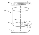
また、本発明者らが更に鋭意検討した結果、上述の[0 0 1]軸と光軸を一致させる方法と同様、図15に示されるように真性複屈折のピーク(例えば、[1 1 0]軸)と光軸を一致させる場合であっても真性複屈折の影響を低減可能であることを発見した。ここで、図15は、図3に示すシミュレーション結果を[1 1 0]軸方向から見たときの真性複屈折を示すシミュレーション結果である。なお、本明細書では真性複屈折のピークの現れる軸として[1 1 0]軸を用いて説明を展開するが、本発明がこれに限定されるものではない。上述したように真性複屈折は12方向にピークを示すものであって、本実施形態では例示的に[1 1 0]軸を用いているに過ぎない。よって、本明細書中に表現される[1 1 0]軸は、[1 0 1]軸及び[0 1 1]軸等の他の11の軸と置換されても良く、[1 1 0]軸はそれら12の軸を総括するものであることに理解されたい。
【0037】
以下、図16及び図17を参照するに、光軸と[1 1 0]軸を一致させた場合に真性複屈折が低減する理由と共に、本発明の別の一態様としての光学系300について説明する。ここで、図16は、本発明の光学系300を示す模式図である。図17は、図16に示す光学系300の概略断面図である。光学系300は2枚の光学素子(平行平板)310及び320とを有し、この2枚の平行平板310及び320の組み合わせにより真性複屈折を低減可能であることを特徴としている。より詳細には、平行平板310及び320は同一の平行平板(即ち、結晶方位に関し同一の方位性並びに同一の厚さを有する)であり、平行平板310及び320は結晶方位に関する[1 1 0]軸が平行平板310及び320の光軸(ここでは、板310,320の面に立てた垂線と一致)と一致するように構成される。
【0038】
このような平行平板310及び320において、光学系300はかかる平行平板310及び320の[1 1 0]軸が光軸Oと一致するように配置されている。更に、平行平板310と平行平板320は、光軸と一致した[1 1 0]軸に垂直な一の軸、例えば、[0 0 1]軸が平行平板310及び320において相対角度を変化させて配置されている(なお、[0 0 1]軸も例示的であり、[1 1 0]軸に垂直な軸はこれに限定されるものではない。)。図16に良く示されるように、本実施形態において平行平板310と平行平板320は各々の[0 0 1]軸が直交する、即ち、[0 0 1]軸の相対角度が90°となるように配置されている。
【0039】
かかる構成において、光学系300は当該光学系300に入射した光線に関し、平行平板310で進んできた(又は、遅れてきた)偏光成分の位相を平行平板320で遅らせる(又は、進ませる)ことにより、かかる偏光成分の位相のずれをキャンセルし真性複屈折の影響を低減している。より詳細には、複屈折には必ず方向があり、それには真相軸と遅相軸がある。進相軸とは、光が進む進行方向と進相軸がなす面、その面内で振動する電界成分をもつ偏光がそれと直交する偏光に対して媒質(本実施形態では、光学素子)を通ることにより位相が進むことである。一方、遅相軸はこれと逆の現象であり、媒質(本実施形態では、光学素子)を通ることにより位相が遅れることである。即ち、一の平行平板310を通過するだけでは偏光成分の位相のずれ、即ち真性複屈折が現れてしまう。しかし、もう一つの平行平板320をかかる平行平板310に対して真相軸と遅層軸が逆転するように、即ち、[1 1 0]軸に直交する軸が直交するように設けることによりかかる位相のずれをキャンセルしている。
【0040】
図18を参照するに、[1 1 0]軸を光軸方向とした2枚の平行平板310及び320に関し、光軸周りに相対角度を変化させることでかかる2枚の平行平板310及び320よりなる光学系300の総合的な真性複屈折を減少させることが理解されるであろう。ここで、図18は、[1 1 0]軸を光軸方向とした2枚の平行平板の光軸周りの相対角度を変化させた場合に発生する真性複屈折を示すシミュレーション結果である。なお、2枚の平行平板の厚さは1cmであり、使用した波長は157nmの場合について示している。図18を参照するに、2枚の平行平板の光軸周りの相対角を変化させることで、かかる2平行平板における真性複屈折が減少することが容易に理解され、また、相対角度が45°以上(90°未満)では真性複屈折は一枚の平行平板を使用したときよりも減少している。更に、2枚の平行平板は、[1 1 0]軸に直交する一の軸(例えば、[0 0 1]軸)の相対角度を90°とすることで真性複屈折の大きさが最小(0nm/cm)とすることができる。
【0041】
また、かかる光学系300の一断面について考えると、一の平行平板が[1 0 0]、[1 1 0]、[0 1 0]軸を含む断面である場合、他方の平行平板は[0 0 1]、[1 1 0]、[0 0 −1]軸を含む断面となる。この光学系300の断面について、光線のうち光軸Oから傾いて入射する光線の成分に関しも本発明の光学系300は真性複屈折の影響を低減している。図19に、[1 0 0]、[1 1 0]、[0 1 0]軸を含む断面と、[0 0 1]、[1 1 0]、[0 0 −1]軸を含む断面に関し、光軸が[1 1 0]軸から傾いた場合の真性複屈折の大きさを示す。図19を参照するに、光軸から光線が傾いた場合、各々の断面に関し真性複屈折の値は−30乃至30°の範囲でほぼ一致している。しかし、図19では、真性複屈折は絶対値を示したものであって、[0 0 1]、[1 1 0]、[0 0 −1]軸を含む断面の真性複屈折の量は−35.26°乃至35.26°では符号が反転している。即ち、かかる−30乃至30°の範囲内では、光軸Oから光線が傾いた場合であっても、かかる2の平行平板310及び320により真性複屈折をキャンセル可能であることを示している。なお、30°(より詳細には、30.9°)はNAが0.8に対応し、本発明の光学系300はNA0.8以上の高NAの光学系に関して好適であることを示唆している。
【0042】
このように、本発明の光学系300は、真性複屈折のピークの軸、即ち、[11 0]軸が光軸と一致とするものの、2枚の平行平板310及び320を組み合わせることで光学系300における真性複屈折を低減している。したがって、かかる光学系300であっても結像性能の向上を達成することができる。また、高NAの光学系においても、光学系300は充分有効であることが検証された。
【0043】
なお、光学系300は、本実施形態において例示的に2枚の平行平板310及び320より構成されるが、光学系300を構成する光学素子の数において限定を有するものではない。光学系300は2以上の、平行平板やレンズや回折光学素子等の光学素子により構成されても良い。しかしながら、光学系300は上述したように偏光成分の位相の差がキャンセル、即ち、光学系300における真性複屈折が相対的に低減されるようにこれら光学素子の[1 1 0]軸と直交する一の軸[0 0 1]軸の相対角度を変化させて配置しなければならないことに留意する必要がある。
【0044】
例えば、図20によく示されるように、3枚の平行平板よりなる光学系300Aは、図16及び図17に示す平行平板320(又は、平行平板310)を2枚に分割することで構成することができる。ここで、図20は、図16及び図17に示す光学系300の変形例としての光学系300Aを示した模式図である。図19において、平行平板320A及び320Bは図16及び図17に示す平行平板320を[1 1 0]軸と垂直な面に関し分割したものであり、図20では例示的にその厚みを平行平板320の半分としている。これにより、平行平板320A及び320Bは、平行平板310に対して[1 1 0]軸と直交する一の軸(例えば、[0 0 1]軸)の相対角度を変化させるとともに、平行平板320A及び320Bにおいて平行平板320と同等の作用を奏する。なお、図20では、平行平板320A及び320Bは平行平板310を挟むように構成されているが、平行平板320A及び320Bは平行平板310のどちらか一方に連続して配置されても良い。このような構成であっても、光学系300Aにおける偏光成分の位相差をキャンセル可能であり、光学系300と同様の効果を得ることができる。なお、光学系300に追加的にもう一枚の平行平板(平行平板310及び320と同一の結晶方位並びに厚みを有する)を[1 1 0]軸が光軸と一致するように設けて、3枚の平行平板よりなる光学系を構成することも可能である。しかし、かかる光学系では、偏光成分の位相差が最小となるように3枚の平行平板の[1 1 0]軸に直交する一の軸(例えば、[0 0 1]軸)の相対角度を変化させて構成すること必要がある。
【0045】
また、光学系300が4枚以上のn(n:偶数)枚の平行平板より構成される系300B(不図示)であれば、上述した平行平板310及び320を1ペアとして、かかる1ペアをn/2個使用して光学系構成すればよい。更に、光学系300が5枚以上のm(m:奇数)枚の平行平板より構成されるのであれば、上述した平行平板310及び320を1ペアとしてかかる1ペアを(m−3)/2個使用すると共に、残りの3枚の平行平板に関し上述した組み合わせを適用し光学系を構成すればよい。
【0046】
以上の実施例では光学系300A、300Bの複数の光学素子として平行平板を例示したが、このような実施形態は、これらの光学素子として、レンズ、回折光学素子の場合も同様に成立し、又、平行平板を含めてこれら複数種の光学素子の複合体で光学系を組む場合にも成立する。
本発明の光学系300は、上述した光学素子100と同様に、投影光学系400に好適である。なお、投影光学系400は、例示的に、4枚の光学部材L1乃至L4より構成されており、再び図2を用いて説明する。なお、図2に示す投影光学系200の光学部材L1乃至L4の数は例示的でありこれに限定されるものでない。本発明の投影光学系400は、投影光学系の倍率が縮小の場合には、投影光学系400の像面P側に位置する光学部材L1及びL2に光学系300の平行平板310及び320が適用される。但し、光学系300を平行平板310及び320の1ペアで一つと考えるのであれば、図2に示す光学部材L1に対して光学系300が適用されると考えても良い。なお、投影光学系400では、図2に示す光学部材L1及びL2は平行平板として実現されることが好ましい。また、投影光学系200は、像面P側で高NAであるなら、像面P側から3枚目以上の光学部材L3にも光学系300を適用しても良い。上述したように、かかる部分に位置する光学部材は光線と光軸Oのなす最大角が光学部材内で大きくなるからであり、より特定的には、かかる最大角が25°以上となる光学部材に関して光学系300を適用することが良い。25°はNAが0.65に対応し、本発明はNA0.65以上の高NAに対して好適である。これにより、マージナル光線(投影光学系400のうち最も光軸より離れた光線)であっても結像性能を悪化させず、投影光学系400の光学特性の向上に寄与する。
【0047】
また、投影光学系400を構成する光学部材のうち、光学系300が適用されていない光学部材L3及びL4に関しては、上述した[1 0 0]軸を光軸と一致させた光学素子、又は、[1 1 1]軸を光軸と一致させた光学素子、又は、これらの組み合わせより光学素子を用いることが好ましい。この場合、上述したように、光軸(即ち、[1 0 0]軸又は[1 1 1]軸)と直交する軸の相対角度を変化させて、投影光学系400の真性複屈折が小さくなるように調節する(例えば、光学素子を光軸周りに回転させる)ことが好ましい。但し、投影光学系400を構成する光学部材L1乃至L4が2の光学系300より実現される場合であっても、これと同様に、真性複屈折が小さくなるように光学系300同士を相対的に調節しても良い。
【0048】
上述した光学系300並びに投影光学系200及び400のような光学系において、かかる光学系全体の複屈折(複屈折による波面間のずれ)が使用波長λの1/4以上になると、複屈折(応力複屈折及び真性複屈折を含む)により結像状態が悪くなるという欠点を有する。例えば、波長λ=157nmのF2エキシマレーザにおいて、光学系全体を通した複屈折の大きさはほぼ40nm以下となるようにしなければ、良好な結像状態を得ることができない。光学系全体の複屈折は、例えば、干渉実験、及び市販の複屈折測定装置により測定可能であり、かかる光学系を調整することが望ましい。
【0049】
以下、坩堝降下法を利用した本発明のCaF2結晶及び光学素子100の製造方法1000について説明する。但し、本発明は坩堝降下法に限定されるものではない。図10に、本発明のCaF2を使用した光学素子100の製造方法のフローチャートを示す。まず、原料として高純度CaF2の合成原料を用意して、CaF2原料とスカベンジャーとを混合する(ステップ1100)。高純度CaF2の合成原料は炭酸カルシウムをフッ酸で処理することによって製造する。本発明はCaF2原石をフッ酸で処理して不純物(例えば、SiO2)を除去する方法を排除するものではないが、高純度CaF2は原石と違って粉末であり、嵩密度が(約10乃至約20μと)非常に少ないので好ましい。なお、CaF2原料とスカベンジャーとを容器(又は坩堝)を混合する時は容器を回転して均一な混合を確保することが好ましい。
【0050】
スカベンジャーとしては、弗化亜鉛、弗化カドミウム、弗化マンガン、弗化ビスマス、弗化ナトリウム、弗化リチウム等、成長させる弗化物より酸素と結合し易いものが望ましい。弗化物原料中に混じっている酸化物と反応して気化し易い酸化物となる物質が選択される。とりわけ弗化亜鉛が望ましいものである。
【0051】
こうして得られた弗化カルシウムの粉末とスカベンジャーの混合物に対して精製処理がなされる(ステップ1200)。精製処理は、不純物(例えば、炭酸)を除去して弗化カルシウムを高純度化する工程であり、脱水、スカベンジング反応、スカベンジャー生成物の除去、溶融及び固化の作用を含む。精製処理においては、混合物は精製炉の坩堝の中に入れられる。その後、ヒーターに通電して坩堝内の混合物を加熱し、脱水を行う。
【0052】
次に、精製した結晶を2次原料として、図示しない結晶成長炉において弗化カルシウムの単結晶を成長させる(ステップ1300)。成長方法は結晶の大きさや使用目的に応じて適当な方法を選択するが、例えば、ブリッジマン法を用いて坩堝を徐々に引き下げ冷却して単結晶を成長させることができる。この際、坩堝の下部に成長させたい面方位、即ち<0 0 1>面を持つ成長の起点となる種結晶を配置することによって、成長する結晶の面方位を制御する(ステップ1310)必要がある。
【0053】
その後、ヒーターに通電して坩堝内の弗化カルシウム原料(結晶)を約1390乃至1450℃程度まで加熱し、弗化カルシウム結晶を完全に溶融する。その後、徐々に坩堝を0.1乃至5.0mm/hの速度で降下させて(所定の温度勾配を通過させ、)溶融した弗化カルシウム結晶を徐冷して種結晶を基にして単結晶を成長させる。
【0054】
続いて、結晶成長したフッ化物単結晶をアニール炉で熱処理する(アニール工程)(ステップ1400)。アニール工程は、成長した弗化カルシウム単結晶を熱処理し、結晶の割れを引き起こす歪みを除去する工程である。成長した単結晶はアニール炉のチャンバーに収納された坩堝内に入れる。
【0055】
アニール工程では、坩堝を約900℃乃至約1000℃に均熱的に加熱して、固体のまま弗化カルシウム結晶の歪を除去する。加熱温度を約1140℃以上にすると構造変化などを引き起こしてしまうので好ましくはない。加熱時間は約20時間以上、より好ましくは、約20乃至約30時間である。アニール工程では、アニールを経ることによって結晶の転位が減る。その後、歪がなくなった状態を維持しながら弗化カルシウム結晶の温度を室温に戻す。
【0056】
その後、弗化カルシウム結晶を必要とされる光学素子100に成形する(ステップ1500)。光学素子100は、レンズ、回折格子、透明平行平面板、光学膜体及びそれらの複合体、例えば、レンズ、マルチレンズ、レンズアレイ、レンチキュラーレンズ、非球面レンズ、回折格子及びそれらの複合体を含む。また、光学素子100は、単体のレンズ等に加えて(例えば、フォーカス制御用の)光センサーなどを含む。必要に応じて、反射防止膜をフッ化物結晶の光学物品表面に設けるとよい。反射防止膜としては、フッ化マグネシウムや酸化アルミニウム、酸化タンタルが好適に用いられ、これらは抵抗加熱による蒸着や電子ビーム蒸着やスパッタリングなどで形成できる。
【0057】
なお、本実施形態においては、面方位を考慮して弗化カルシウム結晶を作成したが、かかる方法に限定されるものではない。例えば、弗化カルシウム結晶をブリッジマン法により製造する場合に、成長方位に優位性をなくし、結晶成長毎に弗化カルシウムの水平面がランダムな面となるように製造しても良い。この場合、結晶成長により得られた弗化カルシウム結晶から、或は、結晶成長により得られ、さらにアニール処理した弗化カルシウム結晶から、<0 0 1>面が平行2平面となるようにかかる弗化カルシウム結晶を切り出し、その後かかる部材を熱処理することによりその光学特性を向上させるでも良い。
【0058】
かかる工程において、<0 0 1>面が平行平面となるように弗化カルシウム結晶を切り出すことを特徴としている。これにより上述した真性複屈折を考慮した光学素子100を製造することができる。
【0059】
また、光学系300に適用可能な光学素子(平行平板310及び320)は、図10に示すステップ1300で坩堝の下部に成長させたい面方位、即ち<1 1 0>面を持つ成長の起点となる種結晶を配置することによって、成長する結晶の面方位を制御する、又は、<1 1 0>面が平行2平面となるように弗化カルシウム結晶を切り出すことでもよい。なお、光学素子の製造方法は、上述した通りであって、ここでの詳細な説明は省略する。
【0060】
以下、図13を参照して、本発明の例示的な露光装置1について説明する。ここで、図13は、本発明の例示的な露光装置1の概略断面図である。露光装置1は、図13に示すように、照明装置10と、レチクル20と、投影光学系30と、プレート40と、ステージ45とを有する。露光装置1は、ステップアンドリピート方式又はステップアンドスキャン方式でレチクル20に形成された回路パターンをプレート40に露光する走査型投影露光装置である。
【0061】
照明装置10は転写用の回路パターンが形成されたレチクル20を照明し、光源部12と照明光学系14とを有する。
【0062】
光源部12は、例えば、光源としてレーザーを使用する。レーザーは、波長約193nmのArFエキシマレーザー、波長約157nmのF2エキシマレーザーなどを使用することができるが、レーザーの種類はエキシマレーザーに限定されず、例えば、YAGレーザーを使用してもよいし、そのレーザーの個数も限定されない。光源部12にレーザーが使用される場合、レーザー光源からの平行光線を所望のビーム形状に整形する光線整形光学系、コヒーレントなレーザー光線をインコヒーレント化するインコヒーレント化光学系を使用することが好ましい。但し、光源部12に使用可能な光源はレーザーに限定されるものではなく、一又は複数の水銀ランプやキセノンランプなどのランプも使用可能である。
【0063】
照明光学系14はマスク20を照明する光学系であり、レンズ、ミラー、ライトインテグレーター、絞り等を含む。例えば、コンデンサーレンズ、ハエの目レンズ、開口絞り、コンデンサーレンズ、スリット、結像光学系の順で整列する等である。照明光学系14は、軸上光、軸外光を問わず使用することができる。ライトインテグレーターは、ハエの目レンズや2組のシリンドリカルレンズアレイ(又はレンチキュラーレンズ)板を重ねることによって構成されるインテグレーター等を含むが、光学ロッドや回折素子に置換される場合もある。
【0064】
レチクル20の上には転写されるべき回路パターン(又は像)が形成され、図示しないレチクルステージに支持及び駆動される。図示しないレチクルステージは、これまた図示を省略した駆動系の作用によりレチクル面に沿って二次元的に移動可能である。なお、レチクルステージの位置座標は、例えば、図示しないレチクル移動鏡を用いた干渉計によって計測され且つ位置制御されるように構成されている。レチクル20から発せられた回折光は投影光学系30を通りプレート40上に投影される。プレート40はウェハや液晶基板などの被処理体でありレジストが塗布されている。レチクル20とプレート40とは共役の関係にある。走査型投影露光装置の場合は、マスク20とプレート40を走査することによりマスク20のパターンをプレート40上に転写する。ステッパー(ステップアンドリピート露光方式の露光装置)の場合はマスク20とプレート40を静止させた状態で露光が行われる。
【0065】
投影光学系30は、1/5乃至1/2の倍率を有し、レチクル20の回路パターンの縮小像をプレート40上に投影する。投影光学系30は、良像域が軸外の円弧である反射屈折系より成り、レチクル20側及びプレート40側において、実質的にテレセントリックとなっている。投影光学系30における複数の屈折光学素子(レンズ、透明板)の全てが蛍石(弗化カルシウム)より成る。露光装置1において投影光学系30は、上述した投影光学系200又は400を適用することが好ましく、かかる投影光学系30は従来の投影光学系よりも結像状態を良好なものとすることができる。なお、投影光学系30の最もプレート40側の光学素子は透明平行平板であり、収差補正上必要に応じて水平面から傾けて設けられる。但し、本発明の投影光学系30は、この他に複数のレンズ素子と少なくとも一枚の凹面鏡とを有する光学系(カタディオプトリック光学系)、複数のレンズ素子と少なくとも一枚のキノフォームなどの回折光学素子とを有する光学系等を使用することができる。色収差の補正が必要な場合には、互いに分散値(アッベ値)の異なるガラス材からなる複数のレンズ素子を使用したり、回折光学素子をレンズ素子と逆方向の分散が生じるように構成したりする。
【0066】
プレート40にはフォトレジストが塗布されている。フォトレジスト塗布工程は、前処理と、密着性向上剤塗布処理と、フォトレジスト塗布処理と、プリベーク処理とを含む。前処理は洗浄、乾燥などを含む。密着性向上剤塗布処理は、フォトレジストと下地との密着性を高めるための表面改質(即ち、界面活性剤塗布による疎水性化)処理であり、HMDS(Hexamethyl−disilazane)などの有機膜をコート又は蒸気処理する。プリベークはベーキング(焼成)工程であるが現像後のそれよりもソフトであり、溶剤を除去する。
【0067】
ステージ45はプレート40を支持する。ステージ45は、当業界で周知のいかなる構成をも適用することができるので、ここでは詳しい構造及び動作の説明は省略する。例えば、ステージ45は図示しない駆動系の作用によりプレート40面に沿って二次元的に移動可能であり、その位置座標は図示しないプレート移動鏡を用いた干渉計によって計測され且つ位置制御されるように構成されている。レチクル20とプレート40は、例えば、走査型投影露光装置の場合には、同期走査され、ステージ45と図示しないレチクルステージの位置は、例えば、レーザー干渉計などにより監視され、両者は一定の速度比率で駆動される。ステージ45は、例えば、ダンパを介して床等の上に支持されるステージ定盤上に設けられ、レチクルステージ及び投影光学系30は例えば、鏡筒定盤は床等に載置されたベースフレーム上にダンパ等を介して支持される図示しない鏡筒定盤上に設けられる。
【0068】
露光において、光源部12から発せられた光線は、照明光学系14によりレチクル20を、例えば、ケーラー照明する。レチクル20を通過してマスクパターンを反映する光は投影光学系30によりプレート40に結像される。露光装置1が使用する投影光学系30は、本発明の光学素子100を含んで紫外光、遠紫外光及び真空紫外光を高い透過率で透過すると共に屈折率均質性や複屈折率が少ないので、高い解像度とスループットで経済性よくデバイス(半導体素子、LCD素子、撮像素子(CCDなど)、薄膜磁気ヘッドなど)を提供することができる。
【0069】
次に、図11及び図12を参照して、上述の露光装置1を利用したデバイスの製造方法の実施例を説明する。図11は、デバイス(ICやLSIなどの半導体チップ、LCD、CCD等)の製造を説明するためのフローチャートである。ここでは、半導体チップの製造を例に説明する。ステップ101(回路設計)ではデバイスの回路設計を行う。ステップ102(マスク製作)では、設計した回路パターンを形成したマスクを製作する。ステップ103(ウェハ製造)ではシリコンなどの材料を用いてウェハを製造する。ステップ104(ウェハプロセス)は前工程と呼ばれ、マスクとウェハを用いてリソグラフィ技術によってウェハ上に実際の回路を形成する。ステップ105(組み立て)は後工程と呼ばれ、ステップ104によって作成されたウェハを用いて半導体チップ化する工程であり、アッセンブリ工程(ダイシング、ボンディング)、パッケージング工程(チップ封入)等の工程を含む。ステップ106(検査)では、ステップ105で作成された半導体デバイスの動作確認テスト、耐久性テストなどの検査を行う。こうした工程を経て半導体デバイスが完成し、これが出荷(ステップ107)される。
【0070】
図12は、ステップ104のウェハプロセスの詳細なフローチャートである。ステップ111(酸化)ではウェハの表面を酸化させる。ステップ112(CVD)では、ウェハの表面に絶縁膜を形成する。ステップ113(電極形成)では、ウェハ上に電極を蒸着などによって形成する。ステップ114(イオン打ち込み)ではウェハにイオンを打ち込む。ステップ115(レジスト処理)ではウェハに感光剤を塗布する。ステップ116(露光)では、露光装置1によってマスクの回路パターンをウェハに露光する。ステップ117(現像)では、露光したウェハを現像する。ステップ118(エッチング)では、現像したレジスト像以外の部分を削り取る。ステップ119(レジスト剥離)では、エッチングが済んで不要となったレジストを取り除く。これらのステップを繰り返し行うことによってウェハ上に多重に回路パターンが形成される。本実施例の製造方法によれば従来よりも高品位のデバイスを製造することができる。
【0071】
以上、本発明の好ましい実施例について説明したが、本発明はこれらの実施例に限定されないことはいうまでもなく、その要旨の範囲内で種々の変形及び変更が可能である。
【0072】
【発明の効果】
本発明の光学素子及び製造方法によれば、かかる光学素子によれば、真性複屈折率に関し[1 1 1]軸に光軸を一致させた場合と[0 0 1]軸に光軸を一致させた場合とを比べると、[0 0 1]軸に光軸を一致させた方が真性複屈折のピークとなる角度を遠くすることができる。従って、<0 0 1>面、即ち、光軸と[0 0 1]軸を一致させた光学素子100の方が、高NAに対して結像性能を悪化させない。また、[0 0 1]軸に光軸を一致させた場合、真性複屈折ピークは臨界角より外側に存在し、たとえ高NAであったとしても複屈折がピークとなることを防止することができる。
【0073】
また、本発明の他の光学系は、真性複屈折を持つ光学素子を少なくとも一つ有する光学系における複屈折をn、使用波長をλとした際に、結像に寄与する全ての光束に対し当該光学系における複屈折の大きさが n < λ/4を満たすので、光学系の結像性能の向上を達成することができる。
【0074】
また、本発明の別の光学系は、真性複屈折のピークの軸、即ち、[1 1 0]軸が光軸と一致とするものの、2枚の平行平板を組み合わせることでかかる光学系における真性複屈折を低減している。したがって、このような光学系であっても結像性能の向上を達成することができる。
【0075】
また、本発明の光学系を有する投影光学系、並びに、かかる光学素子を含む露光装置及びかかる投影光学系を有する露光装置は結像性能に優れ、高品位なデバイスをスループットなどの露光性能良く提供することができる。
【図面の簡単な説明】
【図1】 本発明の光学素子を示す模式図である。
【図2】 図1に示す光学素子を適用した投影光学系を示す概略側面図である。
【図3】 波長157nmにおける弗化カルシウムの真性複屈折とその方位を3次元的に示したシミュレーション結果である。
【図4】 図3に示す[0 0 1]軸及び[0 1 0]軸を通る平面内における真性複屈折とその方位を2次元的に示したシミュレーション結果、並びに[0 0 1]軸に光軸を合わせた場合のかかる光軸と真性複屈折ピークまでの角度を示した図である。
【図5】 結晶面内での光線の角度と真性複屈折の関係を示した図である。
【図6】 図3にしめすシミュレーション結果を[0 0 1]軸方向から見たときの真性複屈折を示すシミュレーション結果である。
【図7】 光軸回りの方位角に対する真性複屈折を示した図である。
【図8】 図2に示す投影光学系を示す概略斜視図である。
【図9】 図2に示す投影光学系の例示的一態様を示した概略斜視図である。
【図10】 本発明のCaF2を使用した光学素子の製造方法のフローチャートを示す。
【図11】 デバイス(ICやLSIなどの半導体チップ、LCD、CCD等)の製造を説明するためのフローチャートである。
【図12】 図11に示すステップ104のウェハプロセスの詳細なフローチャートである。
【図13】 本発明の例示的な露光装置の概略断面図である。
【図14】 図7に示す図に<1 1 1>面における光軸回りの方位角に対する真性複屈折を加えた図である。
【図15】 図3に示すシミュレーション結果を[1 1 0]軸方向から見たときの真性複屈折を示すシミュレーション結果である。
【図16】 本発明の光学系を示す模式図である。
【図17】 図16に示す光学系の概略断面図である。
【図18】 [1 1 0]軸を光軸方向とした2枚の平行平板の光軸周りの相対角度を変化させた場合に発生する真性複屈折を示すシミュレーション結果である。
【図19】 [1 0 0]、[1 1 0]、[0 1 0]軸を含む断面と、[0 0 1]、[1 1 0]、[0 0 −1]軸を含む断面に関し、光軸が[1 1 0]軸から傾いた場合の真性複屈折の大きさを示す。
【図20】 図16及び図17に示す光学系300の変形例としての光学系300Aを示した模式図である。
【符号の説明】
1 露光装置
10 照明装置
20 レチクル
30 投影光学系
40 プレート
45 ステージ
100 光学素子
200 投影光学系[0001]
BACKGROUND OF THE INVENTION
The present invention generally relates to an optical element, and more particularly to calcium fluoride (CaF) used in a short wavelength range from vacuum ultraviolet to far ultraviolet. 2 ), Barium fluoride (BaF) 2 ), Strontium fluoride (SrF 2 The present invention relates to an optical element composed of equiaxed crystals such as
[0002]
[Prior art]
Due to the recent demand for smaller and thinner electronic devices, the demand for miniaturization of semiconductor elements mounted on electronic devices has been increasing, and various proposals have been made to increase the exposure resolution in order to satisfy such requirements. . Since shortening the wavelength of the exposure light source is an effective means for improving the resolution, in recent years, the exposure light source has been changed from a KrF excimer laser (wavelength of about 248 nm) to an ArF excimer laser (wavelength of about 193 nm). F 2 Excimer lasers (wavelength of about 157 nm) are also being put into practical use. Calcium fluoride single crystal (CaF 2 ) Is optimal as an optical material for optical elements such as lenses and diffraction gratings used in exposure optical systems because of its high light transmittance (that is, internal transmittance) in such a wavelength region. Also, barium fluoride single crystal (BaF 2 ) And strontium fluoride single crystal (SrF) 2 ) Has high transmittance, and its application is being studied.
[0003]
Calcium fluoride single crystals are conventionally produced by the crucible descent method (also known as the “Bridgeman method”). Such a method is a method in which a raw material of a crystalline substance is filled in a crucible and the raw material melted by heating with a heater is crystallized by lowering the crucible and cooling. At this time, the crystal orientation of the crystal to be grown is controlled by arranging a seed crystal serving as a starting point of growth having a crystal orientation to be grown at the bottom of the crucible. Calcium fluoride is generally easy to handle with a wall opening of <1 1 1> plane perpendicular to the crystal orientation [1 1 1] axis, and birefringence due to photoelasticity with respect to light rays in the [1 1 1] axis direction. It has the advantage that there is little influence. In the production thereof, calcium fluoride is grown by controlling the plane orientation using a seed crystal oriented in the <1 1 1> plane, or by cutting out the <1 1 1> plane of the crystal to obtain a desired optical element. And was realized as an optical element having a <1 1 1> plane as a light incident plane. As a result, the optical axis of the optical system composed of such an optical element coincides with the [111] axis, which contributes to improving the optical characteristics of the optical element (or optical system).
[0004]
[Problems to be solved by the invention]
However, even though calcium fluoride can grow crystals without ideal stress strain, the potential birefringence (intrinsic birefringence) cannot be ignored when the wavelength used is shortened. However, it has a problem of deteriorating the optical characteristics of the optical element and hence the imaging performance of the exposure apparatus. This was announced by Burnett et al. At 2nd International Symposium on 157 nm Lithography held at Dana Point in May 2001. The maximum value of intrinsic birefringence of calcium fluoride is 6.5 nm / cm at a wavelength of 157 nm, referring to their experimental values, and the direction showing the maximum value is 12 such as the [1 1 0] axial direction. Exists in the direction.
[0005]
In a conventional exposure apparatus, particularly a projection optical system, the above-described optical element using the <1 1 1> plane has a [1 1 1] axis that is the optical axis and a [1 1 0] axis that exhibits the maximum birefringence of 35. Only 26 ° away. For example, in calcium fluoride, the NA of the light beam passing through the [1 1 0] axis is 0.87 at a wavelength of 193 nm and 0.90 at a wavelength of 157 nm. In particular, in recent exposure apparatuses, the NA of projection optical systems tends to increase due to the improvement in resolution, and such NA is mainly in the range of 0.65 to 0.80. Therefore, in the optical element of the projection optical system close to the wafer side where the maximum angle of the light beam is maximized, the light beam passes through a place where the intrinsic birefringence value close to the [1 1 0] axis is large. As a result, it becomes difficult for the conventional exposure apparatus to perform exposure with good imaging performance.
[0006]
[Means for Solving the Problems]
Therefore, an object of the present invention is to provide an optical element and a manufacturing method, an exposure apparatus, and a device manufacturing method that can reduce the influence of intrinsic birefringence at a high NA.
[0007]
Hereinafter, the description will be described particularly for calcium fluoride, but the same can be said for barium fluoride and strontium fluoride, which are equiaxed crystals having the same crystal properties.
[0008]
In order to achieve the above object, an optical element according to one aspect of the present invention has an angle formed between the [0 0 1] axis and the optical axis with respect to the crystal orientation of an equiaxed crystal is less than 10 ° (preferably 0 degrees). ).
[0009]
In the optical element according to one aspect of the present invention, an angle formed between the [0 0 1] axis relating to the crystal orientation of the equiaxed crystal and the optical axis of the optical system used is less than 10 ° (preferably 0 ° ).
[0010]
According to such an optical element, the angle formed by the [0 0 1] axis and the optical axis with respect to the crystal orientation of the calcium fluoride crystal is less than 10 °. According to such an optical element, the intrinsic birefringence has a maximum value when tilted by 45 ° from the [0 0 1] axis. Therefore, when the optical axis is aligned with the [1 1 1] axis and the optical axis is aligned with the [0 0 1] axis with respect to the angle of light rays and intrinsic birefringence in the crystal plane, The angle at which the peak of intrinsic birefringence is reached can be increased by making the optical axis coincide with the 0 0 1] axis. Therefore, the optical element of the <0 0 1> plane, that is, the
[0011]
Further, an optical element manufacturing method according to another aspect of the present invention includes a step of growing an equiaxed crystal, and a step of molding an optical element from the grown equiaxed crystal, The growth step includes a step of controlling the growth so that the plane orientation of the crystal to be grown becomes a <0 0 1> plane. Alternatively, the method includes a step of growing an equiaxed crystal and a step of molding an optical element from the grown equiaxed crystal, wherein the shaping step includes forming the grown equiaxed crystal into < Cut out with respect to 0 0 1> plane. According to such a method for manufacturing an optical element, an optical element in which the optical axis of the light beam coincides with the [0 0 1] axis of calcium fluoride can be manufactured, and an optical element having excellent optical characteristics can be provided. Such an optical element manufacturing method is suitable for the above-described optical element manufacturing method.
[0012]
Furthermore, an optical element as another aspect of the present invention is manufactured by the above-described manufacturing method. According to the optical element manufactured by this manufacturing method, the same operation as the above-described optical element is achieved. In the optical element, it is preferable that the angle between the [0 0 1] axis related to the crystal orientation of the equiaxed crystal and the optical axis of the optical element is less than 10 °.
[0013]
In the optical element described above, the equiaxed crystal is calcium fluoride, barium fluoride or strontium fluoride.
[0014]
Furthermore, a projection optical system as another aspect of the present invention includes any one of the optical elements described above. According to such a projection optical system, the optical element described above is provided and the same operation is achieved. Therefore, such a projection optical system can achieve improvement in imaging performance.
[0015]
Furthermore, a reduction projection optical system according to another aspect of the present invention has any of the optical elements described above in an optical member on the image side. According to the reduction projection optical system, the optical element described above is provided and the same effect is achieved. In the reduction projection optical system, the NA is the largest on the image side, and the present invention is used for such an optical member. By doing so, imaging performance can be improved.
[0016]
Furthermore, in a projection optical system according to another aspect of the present invention, the optical member in which the maximum angle between the light beam and the optical axis is 25 ° or more in the optical element includes any of the optical elements described above. Such a projection optical system is suitable for a projection optical system having the above-described optical element and having the same function and having an angle of 25 ° or more, that is, an NA of 0.65 or more.
[0017]
Furthermore, the projection optical system according to another aspect of the present invention is a projection optical system having the above-described optical element, wherein the [0 1 0] axis perpendicular to the [0 0 1] axis is a feature of the pattern of the object to be projected. 10 degrees or more with respect to the general direction. According to such a projection optical system, it is possible to shift the characteristic direction of the object pattern and the peak direction of intrinsic birefringence around the optical axis in the optical element, and the imaging performance can be improved. The characteristic direction of the object is 0 °, 45 °, or 90 ° with respect to one direction of the object.
[0018]
Furthermore, a projection optical system according to another aspect of the present invention includes n optical elements as described above, and an optical element having a different [0 1 0] axis perpendicular to the [0 0 1] axis of one optical element. The [0 0 1] axis and the [0 1 0] axis perpendicular to each other are arranged so that the n optical elements are shifted around the optical axis so that they are within 90 / n ± 10 °. According to such a projection optical system, good imaging performance can be obtained by shifting the peak direction of intrinsic birefringence around the optical axis in n or more optical elements.
[0019]
Furthermore, an optical system according to another aspect of the present invention is an optical system having at least one optical element having intrinsic birefringence,
When birefringence in the optical system is n and the wavelength used is λ, the magnitude of birefringence in the optical system satisfies n <λ / 4 for all light fluxes that contribute to imaging. . According to such an optical system, since the magnitude of the intrinsic birefringence of the entire optical system is λ / 4 or less due to the relationship between the axis related to the crystal orientation of the equiaxed crystal and the optical axis, the imaging performance is excellent. In such an optical system, the birefringence n has birefringence due to stress, the stress birefringence is substantially 0, and the intrinsic birefringence is smaller than λ / 4. The birefringence n may further satisfy n <λ / 10. The birefringence n may further satisfy n <λ / 20. Each of the optical elements is composed of an equiaxed crystal, and the relationship between the crystal orientation axis of the optical element and the optical axis is such that the intrinsic birefringence in the optical system is λ / 4 or less, preferably λ / 10 or less. It is set as follows. A projection optical system having such an optical system also functions as part of the present invention.
[0020]
Furthermore, an optical system according to another aspect of the present invention has a plurality of angles in which the angle formed by the [1 1 0] axis and the optical axis with respect to the crystal orientation of the equiaxed crystal is less than 10 degrees (preferably 0 degrees). In an optical system having an optical element, the relative angles of one axis orthogonal to the [1 1 0] axis of two or more optical elements are different. Such an optical system is an optical system in which the phase of the polarization component that has been advanced (or delayed) by the optical element with respect to the light incident on the optical system is different in the relative angle of one axis orthogonal to the [1 1 0] axis. By delaying (or advancing) the element, it is possible to cancel the phase shift of the polarization component and reduce the influence of intrinsic birefringence. The two or more optical elements can be replaced with an optical member obtained by dividing the optical element with respect to a plane orthogonal to the [1 1 0] axis. When the optical system includes the two optical elements, a relative angle of an axis orthogonal to the [110] axis of the two optical elements is 90 °. The two optical elements are parallel flat plates having the same thickness or lenses having the same thickness. The equiaxed crystal of the optical system is a fluoride. The equiaxed crystal may be calcium fluoride, barium fluoride or strontium fluoride.
[0021]
Furthermore, as another aspect of the present invention, a projection optical system includes an optical system including two or more optical elements whose optical axes coincide with the above [1 1 0] axis. Furthermore, as another aspect of the present invention, the reduction projection optical system is a reduction projection optical system having an equiaxed crystal as an optical element, wherein the angle of a marginal ray is 24.6 ° or more in the optical element. The optical system according to any one of claims 21 to 25 is provided for the two or more optical elements. Such a projection optical system has the above-described optical system and has the same function. In the optical element other than the two or more optical elements of the projection optical system, the angle formed by the [1 1 1] axis and the optical axis related to the crystal orientation of the equiaxed crystal is less than 10 degrees. Alternatively, the optical element excluding the two or more optical elements of the projection optical system has an angle formed by the [0 0 1] axis related to the crystal orientation of the equiaxed crystal and the optical axis of less than 10 degrees. Alternatively, the optical element excluding the two or more optical elements of the projection optical system has an angle formed by the [1 1 1] axis or the [0 0 1] axis and the optical axis related to the crystal orientation of the equiaxed crystal. It is less than 10 degrees. In addition, the projection optical system has m optical elements with the [0 0 1] axis described above, and the [0 0 1] axis of n (<m) optical elements among the m optical elements. Are substantially coincident with each other, and the [0 0 1] axis of mn optical elements of the individual optical elements is substantially coincident and orthogonal to the [0 0 1] axis of the n optical elements. The difference between the total thickness (axial thickness) of the n optical elements and the total thickness of the mn optical elements is within 10 mm. In such an optical system, intrinsic birefringence is reduced by changing the relative angle of an axis orthogonal to the optical axis of the optical element excluding the two or more optical elements of the projection optical system.
[0022]
The above optical system uses a light source having a wavelength of 200 nm or less. The light source is ArF excimer laser or F 2 Excimer laser.
[0023]
Furthermore, an optical element as another aspect of the present invention is the above-described optical element or optical system which is one of a lens, a diffraction grating, a parallel plate, an optical film body, and a composite thereof. According to such an optical element, the same operation as the above-described optical element is achieved.
[0024]
Furthermore, an exposure apparatus according to another aspect of the present invention uses ultraviolet light, far ultraviolet light, and vacuum ultraviolet light as exposure light, and projects the exposure light onto the object to be processed through the optical system. The object to be processed is exposed. According to such an exposure apparatus, it is possible to expose with good imaging performance, including the optical element described above.
[0025]
Furthermore, a device manufacturing method according to another aspect of the present invention includes a step of projecting and exposing the object to be processed using the exposure apparatus, and a step of performing a predetermined process on the object to be processed that has been projected and exposed. Have. According to such an exposure apparatus, the same effect as the above-described exposure apparatus can be obtained. A device manufacturing method using such an exposure apparatus and a resultant device also function as one aspect of the present invention.
[0026]
Other objects and further features of the present invention will become apparent from the preferred embodiments described below with reference to the accompanying drawings.
[0027]
DETAILED DESCRIPTION OF THE INVENTION
As a result of examining the crystal orientation of the equiaxed crystal and intensively studying the intrinsic birefringence, the present inventors have found that the optical element composed of the equiaxed crystal has a [1 1 1] axis and an optical axis as in the prior art. It was discovered that the effect of intrinsic birefringence can be reduced by matching the [0 0 1] axis with the optical axis, rather than matching the [0 0 1] axis. In the following description, calcium fluoride (CaF) is exemplified as an equiaxed crystal. 2 However, the present invention is not limited to this. The same can be said for barium fluoride and strontium fluoride, which are equiaxed crystals having the same crystal properties.
[0028]
Hereinafter, the
[0029]
As well shown in FIG. 3, CaF 2 Single crystals have a small intrinsic birefringence in the [1 1 1] axis, and from this point of view, it is effective to mold an optical element such as a lens so that the [1 1 1] axis coincides with the optical axis. However, CaF 2 Shows, for example, a peak of intrinsic birefringence (6.5 nm / cm, experimental value by Burnett et al.) Symmetrically in 12 directions including the [1 1 0] axis. For example, in a projection optical system, the NA tends to increase with the recent increase in NA. CaF 2 The <1 1 1> plane of the birefringence has a very small value with respect to the light beam that coincides with the [1 1 1] axis, but when the light beam is tilted from the [1 1 1] axis (that is, the NA increases). In this case, as described above, the inclination is 35.26 ° and the intrinsic birefringence peak is reached. The critical angle of CaF2 at a wavelength of 157 nm is about 39.9 °, and if the [1 1 1] axis is applied to an optical element applied to a high NA optical system, the maximum angle portion of the light beam is the peak of intrinsic birefringence. A projection optical system having such an optical element becomes undesirably deteriorated in imaging performance.
[0030]
Therefore, as well shown in FIG. 1, the
[0031]
In the
[0032]
As shown in FIG. 2, the
[0033]
3, 6, and 7, in the <0 0 1> plane of the
[0034]
On the other hand, referring to FIG. 8, the pattern of the object M on which the projection optical system forms an image typically uses a pattern with a characteristic angle such as 0, 45, and 90 ° in many cases. Here, FIG. 8 is a schematic perspective view showing the projection
[0035]
Further, if the
[0036]
Further, as a result of further intensive studies by the present inventors, as shown in FIG. 15, the intrinsic birefringence peak (for example, [1 1 0) is similar to the above-described method of matching the [0 0 1] axis with the optical axis. It was discovered that the effect of intrinsic birefringence can be reduced even when the optical axis is aligned with the optical axis. Here, FIG. 15 is a simulation result showing intrinsic birefringence when the simulation result shown in FIG. 3 is viewed from the [1 1 0] axis direction. In the present specification, the description is developed using the [1 1 0] axis as the axis where the peak of intrinsic birefringence appears, but the present invention is not limited to this. As described above, intrinsic birefringence has a peak in 12 directions, and in this embodiment, the [1 1 0] axis is merely used as an example. Therefore, the [1 1 0] axis expressed in this specification may be replaced with other 11 axes such as the [1 0 1] axis and the [0 1 1] axis, and [1 1 0]. It should be understood that the axes summarize those 12 axes.
[0037]
Hereinafter, referring to FIG. 16 and FIG. 17, an
[0038]
In such
[0039]
In such a configuration, the
[0040]
Referring to FIG. 18, regarding two parallel
[0041]
Considering one section of the
[0042]
Thus, although the
[0043]
Although the
[0044]
For example, as well shown in FIG. 20, an
[0045]
If the
[0046]
In the above examples, parallel plates are exemplified as the plurality of optical elements of the
The
[0047]
Of the optical members constituting the projection optical system 400, for the optical members L3 and L4 to which the
[0048]
In an optical system such as the
[0049]
Hereinafter, the CaF of the present invention using the crucible descent method 2 A method 1000 for manufacturing the crystal and
[0050]
As the scavenger, zinc fluoride, cadmium fluoride, manganese fluoride, bismuth fluoride, sodium fluoride, lithium fluoride and the like that are more easily bonded to oxygen than the growing fluoride are desirable. A substance that reacts with the oxide mixed in the fluoride raw material to be easily vaporized is selected. In particular, zinc fluoride is desirable.
[0051]
The mixture of calcium fluoride powder and scavenger thus obtained is subjected to a purification treatment (step 1200). The purification treatment is a step of removing impurities (for example, carbonic acid) to make calcium fluoride highly purified, and includes dehydration, scavenging reaction, scavenger product removal, melting and solidification. In the refining process, the mixture is placed in a crucible of a refining furnace. Thereafter, the heater is energized to heat the mixture in the crucible and perform dehydration.
[0052]
Next, using the purified crystal as a secondary material, a single crystal of calcium fluoride is grown in a crystal growth furnace (not shown) (step 1300). As a growth method, an appropriate method is selected according to the size of the crystal and the purpose of use. For example, the crucible is gradually pulled down and cooled using the Bridgman method to grow a single crystal. At this time, it is necessary to control the plane orientation of the crystal to be grown by disposing the seed crystal which is the starting point of the growth having the plane orientation to be grown at the lower part of the crucible, that is, <0 0 1> plane (step 1310). is there.
[0053]
Thereafter, the heater is energized and the calcium fluoride raw material (crystal) in the crucible is heated to about 1390 to 1450 ° C. to completely melt the calcium fluoride crystal. Thereafter, the crucible is gradually lowered at a speed of 0.1 to 5.0 mm / h (passing through a predetermined temperature gradient), and the molten calcium fluoride crystal is gradually cooled to form a single crystal based on the seed crystal. Grow.
[0054]
Subsequently, the crystal-grown fluoride single crystal is heat-treated in an annealing furnace (annealing step) (step 1400). The annealing step is a step of heat-treating the grown calcium fluoride single crystal to remove strain that causes crystal cracking. The grown single crystal is put in a crucible housed in a chamber of an annealing furnace.
[0055]
In the annealing step, the crucible is heated to about 900 ° C. to about 1000 ° C. so as to remove strain of the calcium fluoride crystal while it remains solid. A heating temperature of about 1140 ° C. or higher is not preferable because it causes structural changes and the like. The heating time is about 20 hours or more, more preferably about 20 to about 30 hours. In the annealing step, crystal dislocations are reduced through annealing. Thereafter, the temperature of the calcium fluoride crystal is returned to room temperature while maintaining the state in which the strain is eliminated.
[0056]
Thereafter, calcium fluoride crystals are formed into the required optical element 100 (step 1500). The
[0057]
In the present embodiment, the calcium fluoride crystal is created in consideration of the plane orientation, but the present invention is not limited to this method. For example, when a calcium fluoride crystal is manufactured by the Bridgman method, it may be manufactured such that the azimuth of the growth direction is lost and the horizontal plane of calcium fluoride becomes a random surface for each crystal growth. In this case, from the calcium fluoride crystal obtained by crystal growth or from the calcium fluoride crystal obtained by crystal growth and further subjected to annealing treatment, the fluoride is applied so that the <0 0 1> plane becomes two parallel planes. The optical properties may be improved by cutting out calcium fluoride crystals and then heat-treating such members.
[0058]
In this step, the calcium fluoride crystal is cut out so that the <0 0 1> plane is a parallel plane. Thereby, the
[0059]
Further, the optical elements (
[0060]
Hereinafter, an
[0061]
The
[0062]
The
[0063]
The illumination
[0064]
A circuit pattern (or image) to be transferred is formed on the
[0065]
The projection
[0066]
The
[0067]
The
[0068]
In exposure, the light emitted from the
[0069]
Next, an embodiment of a device manufacturing method using the above-described
[0070]
FIG. 12 is a detailed flowchart of the wafer process in Step 104. In step 111 (oxidation), the wafer surface is oxidized. In step 112 (CVD), an insulating film is formed on the surface of the wafer. In step 113 (electrode formation), an electrode is formed on the wafer by vapor deposition or the like. In step 114 (ion implantation), ions are implanted into the wafer. In step 115 (resist process), a photosensitive agent is applied to the wafer. Step 116 (exposure) uses the
[0071]
The preferred embodiments of the present invention have been described above, but the present invention is not limited to these embodiments, and various modifications and changes can be made within the scope of the gist.
[0072]
【The invention's effect】
According to the optical element and the manufacturing method of the present invention, according to the optical element, when the optical axis coincides with the [1 1 1] axis and the optical axis coincides with the [0 0 1] axis with respect to the intrinsic birefringence. When compared with the case where the optical axis is aligned, the angle at which the peak of intrinsic birefringence is reached can be increased by aligning the optical axis with the [0 0 1] axis. Therefore, the <0 0 1> plane, that is, the
[0073]
The other optical system according to the present invention has an optical system having at least one optical element having intrinsic birefringence, where n is the birefringence and λ is the wavelength used. Since the magnitude of birefringence in the optical system satisfies n <λ / 4, it is possible to improve the imaging performance of the optical system.
[0074]
Further, another optical system according to the present invention has an intrinsic birefringence peak axis, that is, the [1 1 0] axis coincides with the optical axis. Birefringence is reduced. Therefore, even with such an optical system, improvement in imaging performance can be achieved.
[0075]
Further, the projection optical system having the optical system of the present invention, the exposure apparatus including the optical element, and the exposure apparatus having the projection optical system have excellent imaging performance, and provide a high-quality device with high exposure performance such as throughput. can do.
[Brief description of the drawings]
FIG. 1 is a schematic view showing an optical element of the present invention.
FIG. 2 is a schematic side view showing a projection optical system to which the optical element shown in FIG. 1 is applied.
FIG. 3 is a simulation result showing three-dimensionally the intrinsic birefringence and orientation of calcium fluoride at a wavelength of 157 nm.
4 is a simulation result showing two-dimensionally the intrinsic birefringence and its orientation in a plane passing through the [0 0 1] axis and the [0 1 0] axis shown in FIG. 3, and the [0 0 1] axis. It is the figure which showed the angle to this optical axis at the time of match | combining an optical axis and an intrinsic birefringence peak.
FIG. 5 is a diagram showing the relationship between the angle of light rays in a crystal plane and intrinsic birefringence.
6 is a simulation result showing intrinsic birefringence when the simulation result shown in FIG. 3 is viewed from the [0 0 1] axis direction. FIG.
FIG. 7 is a diagram showing intrinsic birefringence with respect to an azimuth angle around the optical axis.
8 is a schematic perspective view showing the projection optical system shown in FIG.
9 is a schematic perspective view showing an exemplary aspect of the projection optical system shown in FIG.
FIG. 10: CaF of the present invention 2 The flowchart of the manufacturing method of the optical element using this is shown.
FIG. 11 is a flowchart for explaining how to fabricate devices (ie, semiconductor chips such as IC and LSI, LCDs, CCDs, and the like).
12 is a detailed flowchart of the wafer process in Step 104 shown in FIG. 11. FIG.
FIG. 13 is a schematic sectional view of an exemplary exposure apparatus of the present invention.
14 is a diagram in which intrinsic birefringence with respect to an azimuth angle around the optical axis in the <1 1 1> plane is added to the diagram shown in FIG.
FIG. 15 is a simulation result showing intrinsic birefringence when the simulation result shown in FIG. 3 is viewed from the [1 1 0] axis direction.
FIG. 16 is a schematic diagram showing an optical system of the present invention.
17 is a schematic sectional view of the optical system shown in FIG.
FIG. 18 is a simulation result showing intrinsic birefringence that occurs when the relative angle around the optical axis of two parallel plates with the [1 1 0] axis as the optical axis direction is changed.
FIG. 19 relates to a cross section including the [1 0 0], [1 1 0], and [0 1 0] axes, and a cross section including the [0 0 1], [1 1 0], and [0 0 -1] axes. , Shows the magnitude of intrinsic birefringence when the optical axis is tilted from the [1 1 0] axis.
20 is a schematic diagram showing an
[Explanation of symbols]
1 Exposure equipment
10 Lighting equipment
20 reticle
30 Projection optical system
40 plates
45 stages
100 optical elements
200 Projection optical system
Claims (4)
前記光学素子の[0 0 1]軸及びそれと等価な軸([0 0 −1]軸、[0 1 0]軸、[0 −1 0]軸、[1 0 0]軸、及び、[−1 0 0]軸)のうち一つの第1の軸と、前記投影光学系の光軸のなす角度が、10°未満であり、
前記光学素子の[0 0 1]軸及びそれと等価な軸であって前記第1の軸と垂直な複数の第2の軸が、前記レチクルのパターンの周期方向に対して、10°以上ずれていることを特徴とする投影光学系。In a projection optical system having an optical element that is an equiaxed crystal and projecting a reticle pattern onto a workpiece,
The [0 0 1] axis of the optical element and its equivalent axis ([0 0 -1] axis, [0 1 0] axis, [0 -1 0] axis, [1 0 0] axis, and [− The angle formed by one first axis of the 1 0 0] axis) and the optical axis of the projection optical system is less than 10 °,
The [0 0 1] axis of the optical element and a plurality of second axes that are equivalent to the axis and perpendicular to the first axis are shifted by 10 ° or more with respect to the periodic direction of the pattern of the reticle. A projection optical system.
Priority Applications (9)
| Application Number | Priority Date | Filing Date | Title |
|---|---|---|---|
| JP2001244970A JP3639807B2 (en) | 2001-06-27 | 2001-07-06 | Optical element and manufacturing method |
| US09/934,947 US7102828B2 (en) | 2001-06-27 | 2001-08-22 | Optical element and manufacturing method thereof |
| TW091108576A TWI244679B (en) | 2001-06-27 | 2002-04-25 | Optical element and manufacturing method therefor |
| KR1020037014060A KR100544394B1 (en) | 2001-06-27 | 2002-06-13 | Optical element and manufacturing method therefor |
| AT02736104T ATE352048T1 (en) | 2001-06-27 | 2002-06-13 | EXPOSURE DEVICE COMPRISING AN OPTICAL ELEMENT MADE OF ISOMETRIC CRYSTAL |
| EP02736104A EP1399766B1 (en) | 2001-06-27 | 2002-06-13 | Exposure apparatus comprising an optical element made of an isometric crystal |
| PCT/JP2002/005952 WO2003003072A2 (en) | 2001-06-27 | 2002-06-13 | Optical element and manufacturing method therefor |
| DE60217673T DE60217673T2 (en) | 2001-06-27 | 2002-06-13 | Exposure device with an isometric crystal optical element |
| US10/684,294 US7262920B2 (en) | 2001-06-27 | 2003-10-10 | Optical element and manufacturing method therefor |
Applications Claiming Priority (3)
| Application Number | Priority Date | Filing Date | Title |
|---|---|---|---|
| JP2001-234254 | 2001-06-27 | ||
| JP2001234254 | 2001-06-27 | ||
| JP2001244970A JP3639807B2 (en) | 2001-06-27 | 2001-07-06 | Optical element and manufacturing method |
Publications (3)
| Publication Number | Publication Date |
|---|---|
| JP2003131002A JP2003131002A (en) | 2003-05-08 |
| JP3639807B2 true JP3639807B2 (en) | 2005-04-20 |
| JP2003131002A5 JP2003131002A5 (en) | 2005-07-28 |
Family
ID=26619804
Family Applications (1)
| Application Number | Title | Priority Date | Filing Date |
|---|---|---|---|
| JP2001244970A Expired - Fee Related JP3639807B2 (en) | 2001-06-27 | 2001-07-06 | Optical element and manufacturing method |
Country Status (8)
| Country | Link |
|---|---|
| US (2) | US7102828B2 (en) |
| EP (1) | EP1399766B1 (en) |
| JP (1) | JP3639807B2 (en) |
| KR (1) | KR100544394B1 (en) |
| AT (1) | ATE352048T1 (en) |
| DE (1) | DE60217673T2 (en) |
| TW (1) | TWI244679B (en) |
| WO (1) | WO2003003072A2 (en) |
Families Citing this family (120)
| Publication number | Priority date | Publication date | Assignee | Title |
|---|---|---|---|---|
| DE10028434B4 (en) * | 2000-06-14 | 2005-09-29 | Ludwig Felser | Steel Building system |
| WO2002031570A1 (en) * | 2000-10-10 | 2002-04-18 | Nikon Corporation | Method of evaluating imaging performance |
| US7239447B2 (en) * | 2001-05-15 | 2007-07-03 | Carl Zeiss Smt Ag | Objective with crystal lenses |
| DE10123725A1 (en) | 2001-05-15 | 2002-11-21 | Zeiss Carl | Objective for microlithographic projection, includes lens element with axis perpendicular to specified fluoride crystal plane |
| DE10210782A1 (en) * | 2002-03-12 | 2003-10-09 | Zeiss Carl Smt Ag | Lens with crystal lenses |
| EP1390783A2 (en) * | 2001-05-15 | 2004-02-25 | Carl Zeiss | Lens system consisting of fluoride crystal lenses |
| US6683710B2 (en) * | 2001-06-01 | 2004-01-27 | Optical Research Associates | Correction of birefringence in cubic crystalline optical systems |
| US20030011893A1 (en) * | 2001-06-20 | 2003-01-16 | Nikon Corporation | Optical system and exposure apparatus equipped with the optical system |
| US6831731B2 (en) * | 2001-06-28 | 2004-12-14 | Nikon Corporation | Projection optical system and an exposure apparatus with the projection optical system |
| US6788389B2 (en) * | 2001-07-10 | 2004-09-07 | Nikon Corporation | Production method of projection optical system |
| US6775063B2 (en) | 2001-07-10 | 2004-08-10 | Nikon Corporation | Optical system and exposure apparatus having the optical system |
| US6844915B2 (en) * | 2001-08-01 | 2005-01-18 | Nikon Corporation | Optical system and exposure apparatus provided with the optical system |
| JPWO2003023480A1 (en) * | 2001-09-07 | 2004-12-24 | 株式会社ニコン | Optical system, exposure apparatus having the optical system, and device manufacturing method |
| US20030070606A1 (en) * | 2001-10-05 | 2003-04-17 | Leblond Nicolas | Preparation of feedstock of alkaline earth and alkali metal fluorides |
| US6995908B2 (en) * | 2001-10-30 | 2006-02-07 | Asml Netherlands B.V. | Methods for reducing aberration in optical systems |
| US7453641B2 (en) * | 2001-10-30 | 2008-11-18 | Asml Netherlands B.V. | Structures and methods for reducing aberration in optical systems |
| US6970232B2 (en) * | 2001-10-30 | 2005-11-29 | Asml Netherlands B.V. | Structures and methods for reducing aberration in integrated circuit fabrication systems |
| DE10162796B4 (en) * | 2001-12-20 | 2007-10-31 | Carl Zeiss Smt Ag | Method for optimizing the imaging properties of at least two optical elements and photolithographic manufacturing method |
| US7075721B2 (en) * | 2002-03-06 | 2006-07-11 | Corning Incorporated | Compensator for radially symmetric birefringence |
| JP2003309059A (en) * | 2002-04-17 | 2003-10-31 | Nikon Corp | Projection optical system and manufacturing method thereof, projection aligner, and exposure method |
| JP4333078B2 (en) * | 2002-04-26 | 2009-09-16 | 株式会社ニコン | Projection optical system, exposure apparatus including the projection optical system, exposure method using the projection optical system, and device manufacturing method |
| US7292388B2 (en) * | 2002-05-08 | 2007-11-06 | Carl Zeiss Smt Ag | Lens made of a crystalline material |
| JP2004045692A (en) * | 2002-07-11 | 2004-02-12 | Canon Inc | Projection optical system, exposure unit, and device manufacturing method |
| US6958864B2 (en) * | 2002-08-22 | 2005-10-25 | Asml Netherlands B.V. | Structures and methods for reducing polarization aberration in integrated circuit fabrication systems |
| DE10345895B4 (en) * | 2002-10-01 | 2015-11-05 | Nikon Corp. | A method of producing an optical element formed by a fluoride crystal |
| US20060171138A1 (en) * | 2003-07-24 | 2006-08-03 | Kenichi Muramatsu | Illuminating optical system, exposure system and exposure method |
| US7239450B2 (en) | 2004-11-22 | 2007-07-03 | Carl Zeiss Smt Ag | Method of determining lens materials for a projection exposure apparatus |
| US7463422B2 (en) * | 2004-01-14 | 2008-12-09 | Carl Zeiss Smt Ag | Projection exposure apparatus |
| JP4776891B2 (en) * | 2004-04-23 | 2011-09-21 | キヤノン株式会社 | Illumination optical system, exposure apparatus, and device manufacturing method |
| EP1851574A1 (en) * | 2005-02-25 | 2007-11-07 | Carl Zeiss SMT AG | Optical system, in particular objective or illumination system for a microlithographic projection exposure apparatus |
| US20110180781A1 (en) * | 2008-06-05 | 2011-07-28 | Soraa, Inc | Highly Polarized White Light Source By Combining Blue LED on Semipolar or Nonpolar GaN with Yellow LED on Semipolar or Nonpolar GaN |
| US8847249B2 (en) * | 2008-06-16 | 2014-09-30 | Soraa, Inc. | Solid-state optical device having enhanced indium content in active regions |
| US8143148B1 (en) | 2008-07-14 | 2012-03-27 | Soraa, Inc. | Self-aligned multi-dielectric-layer lift off process for laser diode stripes |
| US8805134B1 (en) | 2012-02-17 | 2014-08-12 | Soraa Laser Diode, Inc. | Methods and apparatus for photonic integration in non-polar and semi-polar oriented wave-guided optical devices |
| US8259769B1 (en) | 2008-07-14 | 2012-09-04 | Soraa, Inc. | Integrated total internal reflectors for high-gain laser diodes with high quality cleaved facets on nonpolar/semipolar GaN substrates |
| US8284810B1 (en) | 2008-08-04 | 2012-10-09 | Soraa, Inc. | Solid state laser device using a selected crystal orientation in non-polar or semi-polar GaN containing materials and methods |
| EP2319086A4 (en) | 2008-08-04 | 2014-08-27 | Soraa Inc | White light devices using non-polar or semipolar gallium containing materials and phosphors |
| US20100295088A1 (en) * | 2008-10-02 | 2010-11-25 | Soraa, Inc. | Textured-surface light emitting diode and method of manufacture |
| US8247886B1 (en) | 2009-03-09 | 2012-08-21 | Soraa, Inc. | Polarization direction of optical devices using selected spatial configurations |
| US8422525B1 (en) | 2009-03-28 | 2013-04-16 | Soraa, Inc. | Optical device structure using miscut GaN substrates for laser applications |
| US8837545B2 (en) | 2009-04-13 | 2014-09-16 | Soraa Laser Diode, Inc. | Optical device structure using GaN substrates and growth structures for laser applications |
| US8254425B1 (en) | 2009-04-17 | 2012-08-28 | Soraa, Inc. | Optical device structure using GaN substrates and growth structures for laser applications |
| DE112010001615T5 (en) | 2009-04-13 | 2012-08-02 | Soraa, Inc. | Structure of an optical element using GaN substrates for laser applications |
| US8242522B1 (en) | 2009-05-12 | 2012-08-14 | Soraa, Inc. | Optical device structure using non-polar GaN substrates and growth structures for laser applications in 481 nm |
| US8634442B1 (en) | 2009-04-13 | 2014-01-21 | Soraa Laser Diode, Inc. | Optical device structure using GaN substrates for laser applications |
| US8294179B1 (en) | 2009-04-17 | 2012-10-23 | Soraa, Inc. | Optical device structure using GaN substrates and growth structures for laser applications |
| US8416825B1 (en) | 2009-04-17 | 2013-04-09 | Soraa, Inc. | Optical device structure using GaN substrates and growth structure for laser applications |
| US8791499B1 (en) | 2009-05-27 | 2014-07-29 | Soraa, Inc. | GaN containing optical devices and method with ESD stability |
| US10108079B2 (en) | 2009-05-29 | 2018-10-23 | Soraa Laser Diode, Inc. | Laser light source for a vehicle |
| US8427590B2 (en) | 2009-05-29 | 2013-04-23 | Soraa, Inc. | Laser based display method and system |
| US8247887B1 (en) * | 2009-05-29 | 2012-08-21 | Soraa, Inc. | Method and surface morphology of non-polar gallium nitride containing substrates |
| US9250044B1 (en) | 2009-05-29 | 2016-02-02 | Soraa Laser Diode, Inc. | Gallium and nitrogen containing laser diode dazzling devices and methods of use |
| US9829780B2 (en) | 2009-05-29 | 2017-11-28 | Soraa Laser Diode, Inc. | Laser light source for a vehicle |
| US8509275B1 (en) | 2009-05-29 | 2013-08-13 | Soraa, Inc. | Gallium nitride based laser dazzling device and method |
| US9800017B1 (en) | 2009-05-29 | 2017-10-24 | Soraa Laser Diode, Inc. | Laser device and method for a vehicle |
| US20110056429A1 (en) * | 2009-08-21 | 2011-03-10 | Soraa, Inc. | Rapid Growth Method and Structures for Gallium and Nitrogen Containing Ultra-Thin Epitaxial Structures for Devices |
| US9000466B1 (en) | 2010-08-23 | 2015-04-07 | Soraa, Inc. | Methods and devices for light extraction from a group III-nitride volumetric LED using surface and sidewall roughening |
| US8314429B1 (en) | 2009-09-14 | 2012-11-20 | Soraa, Inc. | Multi color active regions for white light emitting diode |
| US8355418B2 (en) | 2009-09-17 | 2013-01-15 | Soraa, Inc. | Growth structures and method for forming laser diodes on {20-21} or off cut gallium and nitrogen containing substrates |
| US8750342B1 (en) | 2011-09-09 | 2014-06-10 | Soraa Laser Diode, Inc. | Laser diodes with scribe structures |
| CN102630349B (en) | 2009-09-18 | 2017-06-13 | 天空公司 | Method power led and using current density operation |
| US9293644B2 (en) | 2009-09-18 | 2016-03-22 | Soraa, Inc. | Power light emitting diode and method with uniform current density operation |
| US9583678B2 (en) | 2009-09-18 | 2017-02-28 | Soraa, Inc. | High-performance LED fabrication |
| US8933644B2 (en) | 2009-09-18 | 2015-01-13 | Soraa, Inc. | LED lamps with improved quality of light |
| US10147850B1 (en) | 2010-02-03 | 2018-12-04 | Soraa, Inc. | System and method for providing color light sources in proximity to predetermined wavelength conversion structures |
| US20110182056A1 (en) * | 2010-06-23 | 2011-07-28 | Soraa, Inc. | Quantum Dot Wavelength Conversion for Optical Devices Using Nonpolar or Semipolar Gallium Containing Materials |
| US8905588B2 (en) | 2010-02-03 | 2014-12-09 | Sorra, Inc. | System and method for providing color light sources in proximity to predetermined wavelength conversion structures |
| US20110186874A1 (en) * | 2010-02-03 | 2011-08-04 | Soraa, Inc. | White Light Apparatus and Method |
| US9927611B2 (en) | 2010-03-29 | 2018-03-27 | Soraa Laser Diode, Inc. | Wearable laser based display method and system |
| US8451876B1 (en) | 2010-05-17 | 2013-05-28 | Soraa, Inc. | Method and system for providing bidirectional light sources with broad spectrum |
| US9450143B2 (en) | 2010-06-18 | 2016-09-20 | Soraa, Inc. | Gallium and nitrogen containing triangular or diamond-shaped configuration for optical devices |
| US8816319B1 (en) | 2010-11-05 | 2014-08-26 | Soraa Laser Diode, Inc. | Method of strain engineering and related optical device using a gallium and nitrogen containing active region |
| US9048170B2 (en) | 2010-11-09 | 2015-06-02 | Soraa Laser Diode, Inc. | Method of fabricating optical devices using laser treatment |
| US8975615B2 (en) | 2010-11-09 | 2015-03-10 | Soraa Laser Diode, Inc. | Method of fabricating optical devices using laser treatment of contact regions of gallium and nitrogen containing material |
| US8786053B2 (en) | 2011-01-24 | 2014-07-22 | Soraa, Inc. | Gallium-nitride-on-handle substrate materials and devices and method of manufacture |
| US9318875B1 (en) | 2011-01-24 | 2016-04-19 | Soraa Laser Diode, Inc. | Color converting element for laser diode |
| US9595813B2 (en) | 2011-01-24 | 2017-03-14 | Soraa Laser Diode, Inc. | Laser package having multiple emitters configured on a substrate member |
| US9025635B2 (en) | 2011-01-24 | 2015-05-05 | Soraa Laser Diode, Inc. | Laser package having multiple emitters configured on a support member |
| US9093820B1 (en) | 2011-01-25 | 2015-07-28 | Soraa Laser Diode, Inc. | Method and structure for laser devices using optical blocking regions |
| US9287684B2 (en) | 2011-04-04 | 2016-03-15 | Soraa Laser Diode, Inc. | Laser package having multiple emitters with color wheel |
| US8686431B2 (en) | 2011-08-22 | 2014-04-01 | Soraa, Inc. | Gallium and nitrogen containing trilateral configuration for optical devices |
| US8971370B1 (en) | 2011-10-13 | 2015-03-03 | Soraa Laser Diode, Inc. | Laser devices using a semipolar plane |
| US8912025B2 (en) | 2011-11-23 | 2014-12-16 | Soraa, Inc. | Method for manufacture of bright GaN LEDs using a selective removal process |
| US9269876B2 (en) | 2012-03-06 | 2016-02-23 | Soraa, Inc. | Light emitting diodes with low refractive index material layers to reduce light guiding effects |
| US9020003B1 (en) | 2012-03-14 | 2015-04-28 | Soraa Laser Diode, Inc. | Group III-nitride laser diode grown on a semi-polar orientation of gallium and nitrogen containing substrates |
| US9343871B1 (en) | 2012-04-05 | 2016-05-17 | Soraa Laser Diode, Inc. | Facet on a gallium and nitrogen containing laser diode |
| US9800016B1 (en) | 2012-04-05 | 2017-10-24 | Soraa Laser Diode, Inc. | Facet on a gallium and nitrogen containing laser diode |
| US10559939B1 (en) | 2012-04-05 | 2020-02-11 | Soraa Laser Diode, Inc. | Facet on a gallium and nitrogen containing laser diode |
| US9088135B1 (en) | 2012-06-29 | 2015-07-21 | Soraa Laser Diode, Inc. | Narrow sized laser diode |
| US9184563B1 (en) | 2012-08-30 | 2015-11-10 | Soraa Laser Diode, Inc. | Laser diodes with an etched facet and surface treatment |
| US9978904B2 (en) | 2012-10-16 | 2018-05-22 | Soraa, Inc. | Indium gallium nitride light emitting devices |
| US8802471B1 (en) | 2012-12-21 | 2014-08-12 | Soraa, Inc. | Contacts for an n-type gallium and nitrogen substrate for optical devices |
| US9166372B1 (en) | 2013-06-28 | 2015-10-20 | Soraa Laser Diode, Inc. | Gallium nitride containing laser device configured on a patterned substrate |
| US8994033B2 (en) | 2013-07-09 | 2015-03-31 | Soraa, Inc. | Contacts for an n-type gallium and nitrogen substrate for optical devices |
| US9520695B2 (en) | 2013-10-18 | 2016-12-13 | Soraa Laser Diode, Inc. | Gallium and nitrogen containing laser device having confinement region |
| US9368939B2 (en) | 2013-10-18 | 2016-06-14 | Soraa Laser Diode, Inc. | Manufacturable laser diode formed on C-plane gallium and nitrogen material |
| US9362715B2 (en) | 2014-02-10 | 2016-06-07 | Soraa Laser Diode, Inc | Method for manufacturing gallium and nitrogen bearing laser devices with improved usage of substrate material |
| US9379525B2 (en) | 2014-02-10 | 2016-06-28 | Soraa Laser Diode, Inc. | Manufacturable laser diode |
| US9419189B1 (en) | 2013-11-04 | 2016-08-16 | Soraa, Inc. | Small LED source with high brightness and high efficiency |
| US9209596B1 (en) | 2014-02-07 | 2015-12-08 | Soraa Laser Diode, Inc. | Manufacturing a laser diode device from a plurality of gallium and nitrogen containing substrates |
| US9871350B2 (en) | 2014-02-10 | 2018-01-16 | Soraa Laser Diode, Inc. | Manufacturable RGB laser diode source |
| US9520697B2 (en) | 2014-02-10 | 2016-12-13 | Soraa Laser Diode, Inc. | Manufacturable multi-emitter laser diode |
| EP3084392A1 (en) | 2014-02-28 | 2016-10-26 | Halliburton Energy Services, Inc. | Integrated computational element using incidence angle manipulation |
| US9564736B1 (en) * | 2014-06-26 | 2017-02-07 | Soraa Laser Diode, Inc. | Epitaxial growth of p-type cladding regions using nitrogen gas for a gallium and nitrogen containing laser diode |
| US9246311B1 (en) | 2014-11-06 | 2016-01-26 | Soraa Laser Diode, Inc. | Method of manufacture for an ultraviolet laser diode |
| US9653642B1 (en) | 2014-12-23 | 2017-05-16 | Soraa Laser Diode, Inc. | Manufacturable RGB display based on thin film gallium and nitrogen containing light emitting diodes |
| US9666677B1 (en) | 2014-12-23 | 2017-05-30 | Soraa Laser Diode, Inc. | Manufacturable thin film gallium and nitrogen containing devices |
| US10938182B2 (en) | 2015-08-19 | 2021-03-02 | Soraa Laser Diode, Inc. | Specialized integrated light source using a laser diode |
| US11437774B2 (en) | 2015-08-19 | 2022-09-06 | Kyocera Sld Laser, Inc. | High-luminous flux laser-based white light source |
| US11437775B2 (en) | 2015-08-19 | 2022-09-06 | Kyocera Sld Laser, Inc. | Integrated light source using a laser diode |
| US10879673B2 (en) | 2015-08-19 | 2020-12-29 | Soraa Laser Diode, Inc. | Integrated white light source using a laser diode and a phosphor in a surface mount device package |
| US9787963B2 (en) | 2015-10-08 | 2017-10-10 | Soraa Laser Diode, Inc. | Laser lighting having selective resolution |
| US10771155B2 (en) | 2017-09-28 | 2020-09-08 | Soraa Laser Diode, Inc. | Intelligent visible light with a gallium and nitrogen containing laser source |
| US10222474B1 (en) | 2017-12-13 | 2019-03-05 | Soraa Laser Diode, Inc. | Lidar systems including a gallium and nitrogen containing laser light source |
| US10551728B1 (en) | 2018-04-10 | 2020-02-04 | Soraa Laser Diode, Inc. | Structured phosphors for dynamic lighting |
| US11239637B2 (en) | 2018-12-21 | 2022-02-01 | Kyocera Sld Laser, Inc. | Fiber delivered laser induced white light system |
| US11421843B2 (en) | 2018-12-21 | 2022-08-23 | Kyocera Sld Laser, Inc. | Fiber-delivered laser-induced dynamic light system |
| US11884202B2 (en) | 2019-01-18 | 2024-01-30 | Kyocera Sld Laser, Inc. | Laser-based fiber-coupled white light system |
| US11228158B2 (en) | 2019-05-14 | 2022-01-18 | Kyocera Sld Laser, Inc. | Manufacturable laser diodes on a large area gallium and nitrogen containing substrate |
| US10903623B2 (en) | 2019-05-14 | 2021-01-26 | Soraa Laser Diode, Inc. | Method and structure for manufacturable large area gallium and nitrogen containing substrate |
Family Cites Families (43)
| Publication number | Priority date | Publication date | Assignee | Title |
|---|---|---|---|---|
| US2934993A (en) * | 1955-11-18 | 1960-05-03 | Benjamin J Chromy | Device for optical examination of gem materials |
| US3904267A (en) * | 1973-07-02 | 1975-09-09 | American Optical Corp | Compensating plate to provide uniformity in interference microscopes |
| JPS5418160U (en) * | 1977-04-14 | 1979-02-06 | ||
| US5042922A (en) * | 1986-05-20 | 1991-08-27 | Hughes Aircraft Company | Method for improvidng the spatial resolution in an integrated adaptive optics apparatus |
| NL8900991A (en) * | 1989-04-20 | 1990-11-16 | Asm Lithography Bv | DEVICE FOR IMAGING A MASK PATTERN ON A SUBSTRATE. |
| US5194344A (en) * | 1991-03-26 | 1993-03-16 | Micron Technology, Inc. | Method of fabricating phase shift reticles including chemically mechanically planarizing |
| US5194346A (en) * | 1991-04-15 | 1993-03-16 | Micron Technology, Inc. | Method of fabricating phase shifting reticles with an accurate phase shift layer |
| JPH0527200A (en) | 1991-07-18 | 1993-02-05 | Fujitsu Ltd | Polarized wave coupler |
| US5308211A (en) * | 1992-06-22 | 1994-05-03 | Bayne Machine Works, Inc. | Residential refuse collection cart lifter with universal features |
| US5538158A (en) * | 1994-05-05 | 1996-07-23 | Toter, Inc. | Rotationally-molded refuse container with integrally-molded handle sealed from communication with refuse-carrying compartment |
| US5795047A (en) * | 1994-12-09 | 1998-08-18 | Matsushita Electric Industrial Co., Ltd. | Projection lens and projection display apparatus |
| US6518210B1 (en) * | 1995-01-06 | 2003-02-11 | Nikon Corporation | Exposure apparatus including silica glass and method for producing silica glass |
| JP3534363B2 (en) * | 1995-07-31 | 2004-06-07 | パイオニア株式会社 | Crystal lens and optical pickup optical system using the same |
| US6680803B2 (en) * | 1996-12-21 | 2004-01-20 | Carl-Zeiss Smt Ag | Partial objective in an illuminating systems |
| JP3413067B2 (en) | 1997-07-29 | 2003-06-03 | キヤノン株式会社 | Projection optical system and projection exposure apparatus using the same |
| JP2000128696A (en) | 1998-10-16 | 2000-05-09 | Nikon Corp | Fluoride single crystal-made raw material for making optical element and production of the same raw material |
| JP3856265B2 (en) | 1998-03-12 | 2006-12-13 | 株式会社ニコン | Optical element manufacturing method, optical element birefringence calculation method, and birefringence determination method |
| US6201634B1 (en) * | 1998-03-12 | 2001-03-13 | Nikon Corporation | Optical element made from fluoride single crystal, method for manufacturing optical element, method for calculating birefringence of optical element and method for determining direction of minimum birefringence of optical element |
| JP2000089450A (en) | 1998-09-09 | 2000-03-31 | Canon Inc | Reticle and projection aligner |
| JP2000086394A (en) | 1998-09-17 | 2000-03-28 | Natl Space Development Agency Of Japan | Control of crystal growth direction of ice and experimental apparatus for crystal growth of ice |
| DE59913116D1 (en) * | 1998-11-30 | 2006-04-20 | Zeiss Carl Smt Ag | HIGH-CAPERTURAL PROJECTION LENS WITH MINIMUM GLARE ERROR |
| DE19942281A1 (en) * | 1999-05-14 | 2000-11-16 | Zeiss Carl Fa | Projection lens has system filter screen, constrictions and bulges, negative lens, and positive lenses |
| JP4345232B2 (en) * | 1998-12-25 | 2009-10-14 | 株式会社ニコン | Catadioptric imaging optical system and projection exposure apparatus provided with the optical system |
| JP2000331927A (en) | 1999-03-12 | 2000-11-30 | Canon Inc | Projection optical system and projection aligner using the same |
| US6421131B1 (en) | 1999-07-02 | 2002-07-16 | Cambridge Research & Instrumentation Inc. | Birefringent interferometer |
| EP1102100A3 (en) * | 1999-11-12 | 2003-12-10 | Carl Zeiss | Catadioptric objective with beamsplitter |
| US6330256B1 (en) * | 2000-02-01 | 2001-12-11 | Raytheon Company | Method and apparatus for non-dispersive face-cooling of multi-crystal nonlinear optical devices |
| JP2001332696A (en) | 2000-05-24 | 2001-11-30 | Nec Corp | Board electric potential detecting circuit and board electric potential generating circuit |
| US7405884B2 (en) * | 2000-12-21 | 2008-07-29 | Olympus Corporation | Optical apparatus |
| WO2002093201A2 (en) * | 2001-05-16 | 2002-11-21 | Corning Incorporated | Preferred crystal orientation optical elements from cubic materials |
| US6683710B2 (en) * | 2001-06-01 | 2004-01-27 | Optical Research Associates | Correction of birefringence in cubic crystalline optical systems |
| US20030011893A1 (en) * | 2001-06-20 | 2003-01-16 | Nikon Corporation | Optical system and exposure apparatus equipped with the optical system |
| US6788389B2 (en) * | 2001-07-10 | 2004-09-07 | Nikon Corporation | Production method of projection optical system |
| US6775063B2 (en) * | 2001-07-10 | 2004-08-10 | Nikon Corporation | Optical system and exposure apparatus having the optical system |
| WO2003009017A1 (en) * | 2001-07-17 | 2003-01-30 | Nikon Corporation | Method for producing optical member |
| US20030023498A1 (en) * | 2001-07-25 | 2003-01-30 | Day Money, Inc. | Method of buying and selling goods and services |
| JP2005508018A (en) | 2001-10-30 | 2005-03-24 | アプティカル リサーチ アソシエイツ | Structure and method for reducing aberrations in optical systems |
| US6995908B2 (en) * | 2001-10-30 | 2006-02-07 | Asml Netherlands B.V. | Methods for reducing aberration in optical systems |
| US7453641B2 (en) * | 2001-10-30 | 2008-11-18 | Asml Netherlands B.V. | Structures and methods for reducing aberration in optical systems |
| US6970232B2 (en) * | 2001-10-30 | 2005-11-29 | Asml Netherlands B.V. | Structures and methods for reducing aberration in integrated circuit fabrication systems |
| US6844972B2 (en) * | 2001-10-30 | 2005-01-18 | Mcguire, Jr. James P. | Reducing aberration in optical systems comprising cubic crystalline optical elements |
| KR100585476B1 (en) * | 2002-11-12 | 2006-06-07 | 에이에스엠엘 네델란즈 비.브이. | Lithographic Apparatus and Device Manufacturing Method |
| US7154582B2 (en) * | 2003-02-14 | 2006-12-26 | Canon Kabushiki Kaisha | Exposure apparatus and method |
-
2001
- 2001-07-06 JP JP2001244970A patent/JP3639807B2/en not_active Expired - Fee Related
- 2001-08-22 US US09/934,947 patent/US7102828B2/en not_active Expired - Fee Related
-
2002
- 2002-04-25 TW TW091108576A patent/TWI244679B/en not_active IP Right Cessation
- 2002-06-13 EP EP02736104A patent/EP1399766B1/en not_active Revoked
- 2002-06-13 AT AT02736104T patent/ATE352048T1/en not_active IP Right Cessation
- 2002-06-13 KR KR1020037014060A patent/KR100544394B1/en not_active IP Right Cessation
- 2002-06-13 WO PCT/JP2002/005952 patent/WO2003003072A2/en active IP Right Grant
- 2002-06-13 DE DE60217673T patent/DE60217673T2/en not_active Expired - Lifetime
-
2003
- 2003-10-10 US US10/684,294 patent/US7262920B2/en not_active Expired - Fee Related
Also Published As
| Publication number | Publication date |
|---|---|
| KR100544394B1 (en) | 2006-01-23 |
| WO2003003072A2 (en) | 2003-01-09 |
| DE60217673T2 (en) | 2007-10-18 |
| US7262920B2 (en) | 2007-08-28 |
| EP1399766B1 (en) | 2007-01-17 |
| TWI244679B (en) | 2005-12-01 |
| EP1399766A2 (en) | 2004-03-24 |
| DE60217673D1 (en) | 2007-03-08 |
| WO2003003072A3 (en) | 2003-10-30 |
| US7102828B2 (en) | 2006-09-05 |
| US20030000453A1 (en) | 2003-01-02 |
| KR20040015179A (en) | 2004-02-18 |
| US20040136084A1 (en) | 2004-07-15 |
| ATE352048T1 (en) | 2007-02-15 |
| JP2003131002A (en) | 2003-05-08 |
Similar Documents
| Publication | Publication Date | Title |
|---|---|---|
| JP3639807B2 (en) | Optical element and manufacturing method | |
| KR20030082451A (en) | Optical system and method for manufacturing the same, projective optical system and method for manufacturing the same, exposure apparatus, and exposure method | |
| JPH10260349A (en) | Image formation optical system for ultraviolet-ray laser | |
| US6813070B2 (en) | Optical member for vacuum ultraviolet, and aligner and device manufacture method using same | |
| KR20100109897A (en) | Optical system | |
| JP2003161882A (en) | Projection optical system, exposure apparatus and exposing method | |
| JP4095376B2 (en) | Exposure apparatus and method, and device manufacturing method | |
| TWI232968B (en) | Projection optical system, exposure apparatus and device fabrication method | |
| US6989060B2 (en) | Calcium fluoride crystal and method and apparatus for using the same | |
| JP2003050349A (en) | Optical system and exposure system provided with the optical system | |
| US20040005266A1 (en) | Optical member, process for producing the same, and projection aligner | |
| US20060087629A1 (en) | Optical lens elements, semiconductor lithographic patterning apparatus, and methods for processing semiconductor devices | |
| US7706074B2 (en) | Projection optical system, method of manufacturing projection optical system, exposure apparatus, and exposure method | |
| JP2004103746A (en) | Device and method for exposure | |
| JP2002293685A (en) | Crystal manufacturing method and apparatus | |
| JP3913122B2 (en) | Projection optical system, exposure apparatus, and device manufacturing method | |
| JP2004157349A (en) | Manufacturing method for optical system, projection optical system, aligner and aligning method | |
| JP2004253583A (en) | Projection optical system, adjustment method and manufacturing method thereof, exposure system, and exposure method | |
| JP2007200937A (en) | Optical element and exposure apparatus equipped therewith, and device manufacturing method | |
| JP2006021967A (en) | Apparatus and method for producing crystal, aligner, and method for manufacturing device | |
| JP2006016229A (en) | Method and apparatus for manufacturing crystal, aligner, and device manufacturing method |
Legal Events
| Date | Code | Title | Description |
|---|---|---|---|
| A521 | Request for written amendment filed |
Free format text: JAPANESE INTERMEDIATE CODE: A523 Effective date: 20041213 |
|
| TRDD | Decision of grant or rejection written | ||
| A01 | Written decision to grant a patent or to grant a registration (utility model) |
Free format text: JAPANESE INTERMEDIATE CODE: A01 Effective date: 20050111 |
|
| A61 | First payment of annual fees (during grant procedure) |
Free format text: JAPANESE INTERMEDIATE CODE: A61 Effective date: 20050117 |
|
| R150 | Certificate of patent or registration of utility model |
Free format text: JAPANESE INTERMEDIATE CODE: R150 |
|
| FPAY | Renewal fee payment (event date is renewal date of database) |
Free format text: PAYMENT UNTIL: 20080121 Year of fee payment: 3 |
|
| FPAY | Renewal fee payment (event date is renewal date of database) |
Free format text: PAYMENT UNTIL: 20090121 Year of fee payment: 4 |
|
| FPAY | Renewal fee payment (event date is renewal date of database) |
Free format text: PAYMENT UNTIL: 20090121 Year of fee payment: 4 |
|
| FPAY | Renewal fee payment (event date is renewal date of database) |
Free format text: PAYMENT UNTIL: 20100121 Year of fee payment: 5 |
|
| FPAY | Renewal fee payment (event date is renewal date of database) |
Free format text: PAYMENT UNTIL: 20110121 Year of fee payment: 6 |
|
| FPAY | Renewal fee payment (event date is renewal date of database) |
Free format text: PAYMENT UNTIL: 20120121 Year of fee payment: 7 |
|
| FPAY | Renewal fee payment (event date is renewal date of database) |
Free format text: PAYMENT UNTIL: 20130121 Year of fee payment: 8 |
|
| FPAY | Renewal fee payment (event date is renewal date of database) |
Free format text: PAYMENT UNTIL: 20140121 Year of fee payment: 9 |
|
| LAPS | Cancellation because of no payment of annual fees |