JP4345232B2 - Catadioptric imaging optical system and projection exposure apparatus provided with the optical system - Google Patents
Catadioptric imaging optical system and projection exposure apparatus provided with the optical system Download PDFInfo
- Publication number
- JP4345232B2 JP4345232B2 JP2000591464A JP2000591464A JP4345232B2 JP 4345232 B2 JP4345232 B2 JP 4345232B2 JP 2000591464 A JP2000591464 A JP 2000591464A JP 2000591464 A JP2000591464 A JP 2000591464A JP 4345232 B2 JP4345232 B2 JP 4345232B2
- Authority
- JP
- Japan
- Prior art keywords
- optical system
- imaging optical
- light
- catadioptric
- mirror
- Prior art date
- Legal status (The legal status is an assumption and is not a legal conclusion. Google has not performed a legal analysis and makes no representation as to the accuracy of the status listed.)
- Expired - Fee Related
Links
Images


Classifications
-
- G—PHYSICS
- G02—OPTICS
- G02B—OPTICAL ELEMENTS, SYSTEMS OR APPARATUS
- G02B17/00—Systems with reflecting surfaces, with or without refracting elements
- G02B17/08—Catadioptric systems
- G02B17/0892—Catadioptric systems specially adapted for the UV
-
- G—PHYSICS
- G02—OPTICS
- G02B—OPTICAL ELEMENTS, SYSTEMS OR APPARATUS
- G02B17/00—Systems with reflecting surfaces, with or without refracting elements
- G02B17/08—Catadioptric systems
- G02B17/0804—Catadioptric systems using two curved mirrors
- G02B17/0808—Catadioptric systems using two curved mirrors on-axis systems with at least one of the mirrors having a central aperture
-
- G—PHYSICS
- G02—OPTICS
- G02B—OPTICAL ELEMENTS, SYSTEMS OR APPARATUS
- G02B17/00—Systems with reflecting surfaces, with or without refracting elements
- G02B17/08—Catadioptric systems
- G02B17/0804—Catadioptric systems using two curved mirrors
- G02B17/0812—Catadioptric systems using two curved mirrors off-axis or unobscured systems in which all of the mirrors share a common axis of rotational symmetry
-
- G—PHYSICS
- G02—OPTICS
- G02B—OPTICAL ELEMENTS, SYSTEMS OR APPARATUS
- G02B17/00—Systems with reflecting surfaces, with or without refracting elements
- G02B17/08—Catadioptric systems
- G02B17/0856—Catadioptric systems comprising a refractive element with a reflective surface, the reflection taking place inside the element, e.g. Mangin mirrors
-
- G—PHYSICS
- G02—OPTICS
- G02B—OPTICAL ELEMENTS, SYSTEMS OR APPARATUS
- G02B3/00—Simple or compound lenses
- G02B3/02—Simple or compound lenses with non-spherical faces
- G02B3/04—Simple or compound lenses with non-spherical faces with continuous faces that are rotationally symmetrical but deviate from a true sphere, e.g. so called "aspheric" lenses
-
- G—PHYSICS
- G03—PHOTOGRAPHY; CINEMATOGRAPHY; ANALOGOUS TECHNIQUES USING WAVES OTHER THAN OPTICAL WAVES; ELECTROGRAPHY; HOLOGRAPHY
- G03F—PHOTOMECHANICAL PRODUCTION OF TEXTURED OR PATTERNED SURFACES, e.g. FOR PRINTING, FOR PROCESSING OF SEMICONDUCTOR DEVICES; MATERIALS THEREFOR; ORIGINALS THEREFOR; APPARATUS SPECIALLY ADAPTED THEREFOR
- G03F7/00—Photomechanical, e.g. photolithographic, production of textured or patterned surfaces, e.g. printing surfaces; Materials therefor, e.g. comprising photoresists; Apparatus specially adapted therefor
- G03F7/70—Microphotolithographic exposure; Apparatus therefor
- G03F7/70216—Mask projection systems
- G03F7/70225—Optical aspects of catadioptric systems, i.e. comprising reflective and refractive elements
Description
技術分野
本発明は、例えば半導体素子や液晶表示素子等をフォトリソグラフィ工程で製造する投影露光の際に好適に使用される反射屈折結像光学系、並びに該反射屈折結像光学系を備えた投影露光装置及び露光方法に関し、特に反射屈折結像光学系内の結像光学系の一要素として反射系を用いることにより、紫外線波長域で0.1μm以下の解像度を有する反射屈折結像光学系等に関する。
背景技術
半導体素子等を製造するためのフォトリソグラフィ工程において、フォトマスク又はレチクル(以下、総称して「レチクル」という)上に形成されたパターン像を投影光学系を介して、フォトレジスト等が塗布されたウエハ又はガラスプレート上などに投影露光する投影露光装置が使用されている。そして、半導体素子等の集積度が向上するにつれて、投影露光装置に使用されている投影光学系に要求される解像力は益々高まっている。この要求を満足するためには、照明光(露光光)の波長を短くすること及び投影光学系の開口数(NA)を大きくすることが必要となる。例えば、照明光の波長が180nm以下の場合は、0.1μm以下の高解像を達成できる。
しかし、照明光の波長が短くなると、光の吸収が大きくなり、実用に耐える硝材の種類は限られてしまい、特に波長が180nm以下になると実用上使える硝材は蛍石だけに限定される。このため、屈折レンズ系のみ、即ち屈折力を有する反射鏡(凹面反射鏡又は凸面反射鏡)を含まないレンズ成分のみで構成された投影光学系では、色収差の補正が不可能となる。
また、投影光学系に求められる光学性能は極めて高いため、諸収差をほぼ無収差にまで補正することが必要となる。しかし、屈折型投影光学系で所望の光学性能を達成するためには多数レンズ成分が必要となり、透過率の低減や製造コストの増大を避けることはできない。
これに対して、凹面反射鏡等のパワー(屈折力)を利用する反射型の光学系、すなわちレンズ成分を含むことなく屈折力を有する反射鏡を含む光学系は、色収差を生じることがなく、ペッツバール和に関してレンズ成分とは符号が逆の寄与を示す。従って、反射光学系と屈折光学系とを組み合わせた光学系、いわゆる反射屈折型の光学系(以下、「反射屈折結像光学系」という)は、レンズ枚数の増加を招くことなく、色収差をはじめ各諸収差をほぼ無収差にまで良好に補正することができる。ここで、反射屈折結像光学系とは、少なくとも1つのレンズ成分と、屈折力を有する少なくとも1つの反射鏡とを含む光学系である。なお、屈折型の光学系や反射型の光学系において、必要に応じて平行平面板や光路偏向用の平面反射鏡などが設けられることは言うまでもない。
しかしながら、投影露光装置の投影光学系の光路中に凹面反射鏡を用いると、レチクル側からこの凹面反射鏡に入射した光が反射されて再び元のレチクル側へ逆進してしまう。このため、凹面反射鏡に入射する光の光路と凹面反射鏡で反射される光の光路とを分離するとともに凹面反射鏡からの反射光をウエハ方向へ導くための技術が、すなわち反射屈折結像光学系により投影光学系を構成する種々の技術が、従来より多く提案されている。
代表的な光路分離の方法として、特公平7−117648号公報には、ハーフミラーや偏光ビームスプリッター等の透過反射面を用いて光路分離を行う方法が提案されている。また、米国特許第4,779,966号公報には、光軸外の光路を用いて中間像を形成し、中間像の形成位置の近傍に光路折り曲げ用の平面鏡を配置して光路分離を行なう方法が提案されている。さらに、米国特許第5,031,976号公報には、中央に開口部を有する2枚の反射鏡を用い、光学系の瞳の近くで光束断面の大きいときに光束が反射され、且つ像面の近くで光束断面の小さいときに光束が中央開口部を通過するように2枚の反射鏡を配置することにより光路分離を行なう方法が提案されている。
しかしながら、特公平7−114648号公報及び米国特許第4,779,966号公報に開示された光路分離方法では、光路分離のために光軸に対して斜設された平面鏡を用いるため、光学系が複数の光軸を有することになる。高精度な光学部品の調整を必要とする投影光学系においては、複数の光軸の位置合わせを高精度に行なうとともに各光軸に対して所望の位置に光学部品をミクロンオーダーで配置することは非常に難しい技術を必要とするため、結果として光学系を製造するためのコストの増大を避けることはできない。
一方、米国特許第5,031,976号公報に開示された光路分離方法を用いると、光学系を構成するすべての光学要素を単一の光軸に沿って配置することができる。その結果、投影光学系において従来から用いられている光学部品の調整方法に従って高精度に光学系を製造することが可能である。この光路分離方法を用いた光学系が、米国特許第5,031,976号公報の他にも、米国特許第5,488,229号公報、米国特許5,650,877号公報、米国特許第5,717,518号公報等に開示されている。
しかしながら、米国特許第5,031,976号公報などに開示された光学系では、2つの反射鏡で全く反射されることなくその中央開口部を通過して像面に達する迷光の発生を回避するために、結像光束のうち光軸を中心とした一部の光束を遮る必要がある。その結果、この結像光束の中心遮蔽に起因して、光学系の結像特性が低下する。従って、米国特許第5,031,976号公報に開示された光路分離方法を投影光学系に適用するには、十分な光学性能を得るため、結像光束の中心遮蔽率(以下、単に「中心遮蔽率」という)を小さく抑えることが重要である。
米国特許5,650,877号公報に開示された光学系では、中間像を形成することなく、物体面(マスク面に対応する面)寄りにハーフミラーを配置し、像面(ウエハ面に対応する面)寄りに中央に開口部を有する反射鏡を配置することによって、中心遮蔽率をある程度小さく抑えている。すなわち、この光学系では、ハーフミラーの採用が必須となる。しかしながら、たとえば波長が180nm以下の露光光を用いる投影光学系に対してこの光学系を適用した場合、半透過薄膜の形成に使用可能な物質が限定されるので、十分な性能のハーフミラーを製造することは困難である。また、ウエハ面に到達する光は1/4以下となってしまうため、スループットの低下は避けられない。
米国特許第5,031,976号公報、米国特許第5,488,229号公報、及び米国特許第5,717,518号公報に開示された光学系では、いずれも第1結像光学系を介して中間像を形成し、その形成位置の近傍に中央開口部を有する第1の反射鏡を配置し、さらに像面の近傍に中央開口部を有する第2の反射鏡を配置することによって、中心遮蔽率をある程度小さく抑えている。
しかしながら、これらの公報に開示された光学系は、以下のような不都合を有する。
一般に、投影光学系が0.1μm以下の高解像を得るには、露光光としてF2レーザ(波長157nm)を用いたとしても、0.7以上の像側NAが必要となる。また、半導体チップのサイズおよびスループットを考えると、像側のイメージサークルが直径10mmを切ることは現在のところ考えられない。さらに、像側のWD(ワークディスタンス:投影光学系の最もウエハ側のレンズ面とウエハとの間の軸上空気間隔)も、露光時のレジスト(ウエハに塗布された)からのアウトガスの影響やウエハステージの駆動の影響を考えると、大幅に小さくすることはできない。
米国特許第5,650,877号公報に開示された光学系では、中間像の形成位置の近傍に厚肉レンズを配置するとともに第2の反射鏡である裏面反射鏡の屈折部に厚肉レンズを採用し、従来から知られている厚肉レンズの色収差補正を利用して、第1結像光学系で発生する色収差の補正を行っている。しかしながら、この光学系では、投影光学系に求められる上述の要件(像側NA、イメージサークル径、像側のWDなど)を満たそうとすると、裏面反射鏡の屈折部の厚さが大きくなり、この屈折部の厚さに比例して裏面反射鏡の径が著しく大きくなる。その結果、製造が困難になるばかりでなく、製造コストが飛躍的に増大してしまう。
また、この光学系では物体側(像側)が無限遠に近いことを想定しているので第1結像光学系の屈折力が小さく、第1結像光学系における色収差の発生もあまり大きくないため、厚肉レンズによりある程度良好な色収差補正を達成している。しかしながら、全系として0.15〜0.4程度の縮小倍率が要求される投影光学系に適用する場合、第1結像光学系の屈折力が増大させざるを得ず、第1結像光学系における色収差の発生の増大を避けることはできない。その結果、この光学系において、特に2つの反射鏡の径および厚さを現実的な大きさに保ったまま、色収差を良好に補正することは困難である。
米国特許第5,488,229号公報に開示された光学系は、米国特許第5,031,976号公報に開示された光学系の変形であり、光源としてArFエキシマレーザ(発振波長193nm)を用いるレーザリペア装置(レーザ加工により半導体回路の修正を行う装置)のための光学系を想定してその最適化を行なったものである。この光学系では、厚肉レンズを用いることなく、2枚の裏面反射鏡を用いることにより色収差補正を行なっている。しかしながら、中間像の形成位置の近傍に配置される凹面鏡が色収差補正の目的から裏面反射鏡であるため、0.7以上の像側NAを達成するとともに像側において所要の大きさのイメージサークルを達成するには、凹面鏡の径が著しく大きくなり、半導体露光装置等の投影光学系としては実現可能な光学解とはなり得ない。
米国特許第5,717,518号公報に開示された光学系では、0.8の像側NAを達成している。しかしながら、米国特許第5,488,229号公報に開示された光学系と同様に、中間像の形成位置の近傍に配置される凹面鏡が色収差補正の目的から裏面反射鏡であるため、像側において所要の大きさのイメージサークルを達成するには、凹面鏡の径が著しく大きくなり現実的ではない。また、この従来技術では、良好な色収差補正を行なうために、石英ガラスや螢石等の複数の硝材を用いて光学系を構成している。このため、この光学系では、波長が180nm以下の露光光を用いることはできず、実質的にはArFエキシマレーザ光が使用可能な最短の波長光である。
また、180nm以下の波長の露光光を用いる光学系においては、十分な屈折率を得るという観点から屈折部材として蛍石を用いることになるが、裏面反射コートを施した蛍石レンズを用いた場合、以下のような不都合を生じる可能性がある。すなわち、このような波長域の光を反射するコートはその膜材料が限定され光吸収が比較的大きくなることから、コートに吸収された大きな光エネルギーが熱として蛍石レンズに伝播する。その結果、熱膨張率が大きい蛍石は、露光中にそのレンズ面形状が変化し、結像性能を劣化させるという傾向が生じ易い。
発明の開示
本発明は、上記問題に鑑みてなされたものであり、例えば波長が180nm以下の紫外領域の照明光を用いた場合にも、少ないレンズ枚数で、反射鏡の大型化を招くことなく、所要の大きさの像側NA及びイメージサークルを得ることができ、例えば0.1μm以下の高解像を達成することのできる反射屈折結像光学系及び該光学系を備えた投影露光装置等を提供することを目的とする。
第1発明に係る反射屈折結像光学系は、第1面の一次像を形成するための屈折型の第1結像光学系と、前記一次像からの光に基づいて前記第1面の二次像を縮小倍率で第2面上に形成するための反射屈折型の第2結像光学系とを備えた反射屈折結像光学系であって、前記第1結像光学系は、第1面側から順に、正の屈折力を有する第1レンズ群と、開口絞りと、正の屈折力を有する第2レンズ群とを有し、前記第2結像光学系は、凹面状に形成された表面反射面を有し且つ中央に第1の光通過部を有する主鏡と、中央に第2の光通過部を有する反射面を備えた副鏡と、該副鏡の前記主鏡側に隣接して配置されて負の屈折力を有するレンズ成分とを有し、前記一次像からの光が前記主鏡の前記第1の光通過部および前記レンズ成分を介して前記副鏡で反射され、前記副鏡で反射された光が前記レンズ成分を介して前記主鏡で反射され、前記主鏡で反射された光が前記レンズ成分および前記副鏡の前記第2の光通過部を介して前記第2面上に前記二次像を形成し、前記反射屈折結像光学系を構成するすべての屈折光学部材は同じ屈折率を有する光学材料により形成され、前記第1結像光学系の結像倍率をβ1とし、前記第2結像光学系の結像倍率をβ2とするとき、
0.7<|β1/β2|<3.5・・・(2)
の条件を満足する。
上記反射屈折結像光学系では、第1結像光学系を介して、第1面(物体面)の一次像すなわち中間像を形成する。そして、中間像の形成位置の近傍に、凹面状に形成された表面反射面を有し且つ中央に第1の光通過部(中央開口部)を有する主鏡を配置して、この主鏡の中央開口部の径を小さく抑えることにより、中心遮蔽率を小さく抑えて結像性能の低下を回避している。さらに、第2面(像面)の近傍に、中央に第2の光通過部(中央開口部)を有する反射面を備えた副鏡と、その主鏡側に隣接して配置されたレンズ成分とを配置して、この副鏡の中央開口部を第2面に近づけることのできる構成を採用することにより、中心遮蔽率を小さく抑えて結像性能の低下を回避している。
前述したように、本発明の光学系を投影露光装置の投影光学系に適用する場合、0.1μm以下の高解像を得るには、波長が180nm以下の露光光を使用する必要がある。したがって、第1発明では、反射屈折結像光学系を構成するすべての屈折光学部材を、同じ屈折率を有する光学材料によって、例えばF2レーザ光を十分な透過率で透過させることのできる単一の硝材によって形成している。また、副鏡の主鏡側に隣接して配置されるレンズ成分の屈折力を負屈折力にすることにより、1次の色収差補正を良好に行なうことができる。
第2発明に係る反射屈折結像光学系は、第1面の一次像を形成するための屈折型の第1結像光学系と、前記一次像からの光に基づいて前記第1面の二次像を縮小倍率で第2面上に形成するための反射屈折型の第2結像光学系とを備えた反射屈折結像光学系であって、前記第1結像光学系は、第1面側から順に、正の屈折力を有する第1レンズ群と、開口絞りと、正の屈折力を有する第2レンズ群とを有し、前記第2結像光学系は、凹面状に形成された表面反射面を有し且つ中央に第1の光通過部を有する主鏡と、中央に第2の光通過部を有する反射面を備えた副鏡と、該副鏡の前記主鏡側に隣接して配置されたレンズ成分とを有し、前記一次像からの光が前記主鏡の前記第1の光通過部および前記レンズ成分を介して前記副鏡で反射され、前記副鏡で反射された光が前記レンズ成分を介して前記主鏡で反射され、前記主鏡で反射された光が前記レンズ成分および前記副鏡の前記第2の光通過部を介して前記第2面上に前記二次像を形成し、前記反射屈折結像光学系を構成するすべての屈折面および反射面のうちの少なくとも1つの面は非球面形状に形成され、前記第1結像光学系の結像倍率をβ1とし、前記第2結像光学系の結像倍率をβ2とするとき、
0.7<|β1/β2|<3.5・・・(2)
の条件を満足する。
上記反射屈折結像光学系では、反射屈折結像光学系を構成するすべての屈折面および反射面のうち少なくとも1つの面を非球面形状に形成している。この構成により、主鏡や副鏡を実現可能な大きさに抑えつつ、十分な結像性能を有する光学系を達成している。
以上説明した第1及び第2発明の反射屈折結像光学系によれば、たとえばF2レーザ光のように波長が180nm以下の光を用いた場合にも、特に主鏡の大型化を招くことなく、所要の大きさの像側NAおよびイメージサークルを確保することができ、たとえば0.1μm以下の高解像を達成することのできる反射屈折結像光学系を少ないレンズ枚数で実現することができる。
なお、本発明(第1発明および第2発明)の光学系において、副鏡に隣接して配置されたレンズ成分の屈折面上に副鏡の反射面を設けて、副鏡とレンズ成分とで裏面反射鏡を構成することが好ましい。この構成により、副鏡の保持機構を第2面側へ突出させることなく、副鏡を、ひいてはその中央開口部をさらに第2面に近づけることができる。その結果、副鏡の中央開口部の径を、ひいては中心遮蔽率をさらに小さく抑えて、結像性能の低下をさらに良好に回避することができる。
また、本発明の光学系においては、副鏡の反射面が主鏡側に凹面を向けた形状に形成されていることが好ましい。この構成により、主鏡の径を大きくすることなく、中心遮蔽率をさらに小さく抑えることができる。
また、本発明の光学系においては、副鏡に隣接して配置されたレンズ成分の主鏡側の屈折面が主鏡側に凹面を向けた形状に形成されていることが好ましい。この構成により、良好な色収差補正を達成することができる。
また、良好な色収差補正を達成するためには、以下の条件式(1)を満足することが好ましい。
0.03<D/|R|<1.0…(1)
ここで、Rは、副鏡に隣接して配置されたレンズ成分の主鏡側の屈折面の曲率半径である。また、Dは、副鏡の有効径である。
条件式(1)の上限値を上回ると、コマ収差および球面収差の高次収差が発生し、大きな開口数を実現することができなくなるので好ましくない。一方、条件式(1)の下限値を下回ると、副鏡を実現可能な大きさに保ったまま色収差を良好に補正することができなくなるので好ましくない。なお、条件式(1)の上限値を0.5とし、下限値を0.07とすることにより、色収差と他の諸収差とを同時にさらに良好に補正することが可能となる。
ところで、露光波長が180nm以下になると、レンズ成分の表面に施される反射防止コート用の膜材料は限られる。その結果、反射防止コートとして十分な性能を得ることができなくなるため、レンズ面のような透過面の数を極力少なくする必要がある。そこで、本発明においては、主鏡と副鏡との間の光路中に配置される屈折光学部材が副鏡に隣接して配置されたレンズ成分のみであることが好ましい。この構成により、レンズ枚数(ひいては透過面の数)の削減を達成し、光学系の透過率を向上させることができる。ただし、この構成は、副鏡と第2面との間の光路中に平行平面板などを配置することを妨げるものではない。
また、本発明の光学系では、第2結像光学系中の屈折面および反射面のうちの少なくとも1つの面を非球面形状に形成することにより、主鏡および副鏡の大型化、並びに中心遮蔽率の増大を避けることが可能となり、結果として十分な結像性能を有し且つ実現可能な光学解を提供することができる。
また、本発明の光学系では、第1結像光学系中の屈折面のうちの少なくとも1つの面を非球面形状に形成することにより、0.1μm以下の高解像を実現しつつ、レンズ枚数の削減を達成して光学系の透過率をさらに向上させることができる。
さらに、第2発明の光学系では、第2結像光学系中の屈折面および反射面のうちの少なくとも1つの面が非球面形状に形成され、第1レンズ群および第2レンズ群の各々が少なくとも1つの非球面形状の屈折面を有することが好ましい。この構成により、反射屈折結像光学系を構成するレンズ枚数を削減することができ、波長が180nm以下の光を露光光として用いることが可能となる。
また、本発明の光学系では、反射屈折結像光学系を構成するすべてのレンズのうちの少なくとも80%の数のレンズは、一方の屈折面が非球面形状に形成され且つ他方の屈折面が球面形状に形成された片側非球面レンズであることが望ましい。この構成により、光学系の大きさ、結像性能、透過率、照射熱による収差変動等を考慮した上で、0.1μm以下の高解像を有する理想的な光学系を実現することができる。また、いわゆる片側非球面レンズを用いることにより、球面形状のレンズ面を基準として非面状のレンズ面との偏芯を容易に調整することが可能である。
さらに、本発明の光学系では、反射屈折結像光学系を構成するすべての屈折光学部材を螢石で形成することにより、例えばF2レーザ光(157nm)のような波長が180nm以下の露光光を使用することが可能となり、0.1μm以下の高解像を実現することができる。
また、本発明の光学系では、反射屈折結像光学系を第1面側および第2面側にテレセントリックな光学系に構成することが好ましい。このように、反射屈折結像光学系を両側テレセントリックに構成することにより、第1面に配置されるマスクや第2面に配置されるウエハなどの光軸方向のずれによる像歪みを無視することのできる微小量に抑えることができる。加えて、第1レンズ群の後側焦点位置の近傍に開口絞りを配置することにより、各視野の開口数が互いに同一となる理想的な両側テレセントリック光学系を実現することができる。
条件式(2)は、第1結像光学系の結像倍率β1と第2結像光学系の結像倍率β2との比β1/β2について適切な範囲を規定している。条件式(2)を満足することにより、第1結像光学系のレンズ成分によって発生する収差と、第2結像光学系の反射鏡等で発生する収差とをバランス良く相殺(キャンセル)することができ、0.1μm以下の高解像を実現することができる。但し、中間像が屈折光学部材中に形成される場合、その屈折光学部材は第1結像光学系に属するものとする。
条件式(2)の上限値を上回ると、第2結像光学系で発生する収差が大きくなり、特に球面収差、コマ収差、色収差の良好な補正が困難となるので好ましくない。一方、条件式(2)の下限値を下回ると、第1結像光学系で発生する収差が大きくなり、全長の大型化を避けることができなくなるので好ましくない。なお、光学系のさらなる小型化と十分な結像性能の達成とを考慮すると、条件式(2)の上限値を2.5とし、下限値を0.85とすることが望ましい。また、投影露光装置の投影光学系に適用する場合には、全系の結像倍率(β1×β2)を0.12〜0.33の範囲に設定することにより、マスクの大きさや精度を実現可能な範囲に設定することができる。
第3発明に係る反射屈折結像光学系は、第1面の中間像を形成するための屈折型の第1結像光学系と、前記中間像からの光に基づいて前記第1面の最終像を縮小倍率で第2面上に形成するための反射屈折型の第2結像光学系とを備えた反射屈折結像光学系であって、前記第1結像光学系は、前記第1面側から順に、正屈折力の第1レンズ群と、開口絞りと、正屈折力の第2レンズ群とを有し、前記第2結像光学系は、中央部に第1光通過部を有する凹面状の第1反射面からなる主鏡と、中央部に第2光通過部を有する第2反射面からなる副鏡と、前記第1反射面及び前記第2反射面から離間されている屈折部材とを有し、前記第1結像光学系からの光が前記主鏡の前記第1光通過部と前記屈折部材とを介して前記第2反射面で反射され、前記第2反射面で反射された光が前記屈折部材を介して前記第1反射面で反射され、前記第1反射面で反射された光が前記屈折部材と前記副鏡の前記第2光通過部とを介して前記第2面上に最終像を形成し、前記第1結像光学系の結像倍率をβ1とし、前記第2結像光学系の結像倍率をβ2とするとき、
0.6<|β1/β2|<3.5・・・(4)
の条件を満足する。
上記反射屈折結像光学系では、第1結像光学系の第1レンズ群と第2レンズ群とを介して、第1面の中間像(1次像)を形成する。そして、中間像の形成位置の近傍に、中央に第1光通過部(中央開口部)を有し、且つ負屈折力(すなわち凹面状)の第1反射面を有する主鏡を配置して、この主鏡の中央開口部の径を小さく抑えることにより、中心遮蔽率を小さく抑えて結像性能の低下を回避している。さらに、第2面(ウエハ面、即ち最終像面)近傍に、第2光通過部(中央開口部)を有する副鏡とその主鏡側に離間して屈折部材とを配置して、この副鏡の中央開口部を第2面に近づけることができる構成を採用し、副鏡を出来る限り光軸方向に薄い構成とすることで、中心遮蔽率を小さく抑えて結像性能の低下を回避している。
上記第3発明の反射屈折結像光学系によれば、たとえばF2レーザ光のように波長が180nm以下の光を用いた場合にも、特に主鏡の大型化を招くことなく、所要の大きさの像側NAおよびイメージサークルを確保することができ、たとえば0.1μm以下の高解像を達成することのできる反射屈折結像光学系を少ないレンズ枚数で実現することができる。
また、第3発明の光学系では、前記屈折部材は負の屈折力を有し、以下の条件式(3)を満足することが好ましい。
−85<f1/d1<−10…(3)
ここで、f1は前記屈折部材の焦点距離、d1は前記副鏡と前記屈折部材との光軸に沿った間隔をそれぞれ表している。条件式(3)は色収差を良好に補正するための条件を規定している。条件式(3)の上限値を上回ると、各波長ごとの像面湾曲のズレが大きくなり良好な色収差補正ができなくなる。また、色コマ収差等の高次収差も発生してしまうので好ましくない。逆に、条件式(3)の下限値を下回ると、1次の色収差が補正不足となり好ましくない。なお、条件式(3)の下限値を−75とし、上限値を−20とすることにより、広い波長域に対してさらに良好に色収差補正を行なうことができる。
また、第3本発明の光学系では、前記屈折部材は、前記第2面側に凹面を向けた屈折面を有することが好ましい。さらに好ましくは、前記屈折部材はメニスカス形状であることが望ましい。この場合、屈折部材の第1面側の屈折面及び第2面側の屈折面においては、主鏡で反射された後に第2面へ向う光束の入射角及び射出角を比較的小さくでき、大きな開口数の光束を第2面上へ導く場合であっても、これらの屈折面での高次収差発生を抑えることが可能となる。また、前記屈折部材は、前記第2面側の屈折面が前記第1面側の屈折面よりも大きな負の屈折力を有することが好ましい。この場合、光線レンズヘの入射角及び射出角を小さくすることができ、高次収差の発生を防ぐことができる。
条件式(4)は第1結像光学系の結像倍率と第2結像光学系の結像倍率との適切な比を規定している。条件式(4)を満足することで、第1結像光学系のレンズ成分により発生する収差と、第2結像光学系の反射鏡等で発生する収差とをバランス良く相殺(キャンセル)することができ、0.1μm以下の高解像を実現できる。但し、中間像が屈折光学部材中に形成される場合、その屈折光学部材は第1結像光学系に属するものとする。
条件式(4)の上限値を上回ると、第2結像光学系で発生する収差が大きくなり、特に球面収差、コマ収差、色収差の良好な補正が困難となるので好ましくない。一方、条件式(4)の下限値を下回ると、第1結像光学系で発生する収差が大きくなり、全長の大型化を避けることができなくなるので好ましくない。なお、光学系のさらなる小型化と十分な結像性能の達成とを考慮すると、条件式(4)の上限値を2.5とし、下限値を0.85とすることが望ましい。また、投影露光装置の投影光学系に適用する場合には、全系の結像倍率(β1×β2)を0.12〜0.33の範囲に設定することにより、マスクの大きさや精度を実現可能な範囲に設定することができる。
また、第4発明に係る反射屈折結像光学系は、第1面の中間像を形成するための第1結像光学系と、前記中間像からの光に基づいて前記第1面の最終像を縮小倍率で第2面上に形成するための第2結像光学系とを備えた反射屈折結像光学系であって、前記第2結像光学系は、中央部に第1光通過部を有する凹面状の第1反射面を備える主鏡と、中央部に第2光通過部を備える第2反射面を備える副鏡とを有し、前記主鏡及び前記副鏡は、前記第1光通過部へ向かう光が前記第1光通過部を介して前記第2反射面で反射され、前記第2反射面で反射された光が前記第1反射面で反射され、前記第1反射面で反射された光が前記副鏡の前記第2光通過部を通過するように位置決めされ、前記反射屈折結像光学系は、前記第1及び第2反射面で反射されずに前記第2面へ向かう光を遮蔽するための中心遮蔽部材と、開口径が可変に構成された可変開口絞りとを備え、前記中心遮蔽部材と前記可変開口絞りとは、前記反射屈折結像光学系の光軸方向で互いに異なる位置に配置される。
第4発明の光学系では、近軸瞳位置(近軸主光線が光軸と交差する位置)の近傍に中心遮蔽部材を配置することによって、全ての像高(物体高)の光束に関する不要光を効果的に遮光することができる。そして、中心遮蔽部材とは異なる光軸方向の位置に可変開口絞りを配置することにより、可変開口絞りの機械構造と中心遮蔽部材を保持する機構との機械的干渉を避けやすくすると共に、可変開口絞りの開口径を変化させた場合に全ての像高(物体高)における口径食の影響、即ちあらゆる像高(物体高)における光束間の開口数の差を実用上十分に抑えることができる。
ここで、可変開口絞りと中心遮蔽部材とを同じ位置に配置した場合には、可変開口絞りと中心遮蔽部材との機械的な干渉を招くばかりか、可変開口絞りの開口径を変化させた際に像高(物体高)の違いによる開口数の差を生じるため好ましくない。このとき、像高(物体高)の違いによる開口数の差を防ぐためには、瞳の像面湾曲を完全に補正することが考えられるが、この場合には全長の長大化やレンズ枚数の増加などの反射屈折結像光学系の複雑化を招くため好ましくない。
また、第4発明の光学系において、前記第1結像光学系は、前記第1面側から順に正屈折力の第1レンズ群と前記可変開口絞りと正屈折力の第2レンズ群とを備え、前記第2結像光学系は、前記主鏡及び前記副鏡とを備え、前記中心遮蔽部材は、前記第1結像光学系中に配置されるものとできる。
上記光学系でも、第1結像光学系において、主鏡及び副鏡を含む第2結像光学系に供給される全ての像高の光束に関する不要光を効果的に遮光することができ、可変開口絞りの機械構造と中心遮蔽部材を保持する機構との機械的干渉を避けやすくすると共に、可変開口絞りの開口径を変化させた場合に全ての像高(物体高)における口径食の影響を実用上十分に抑えることができる。なお、上記構成において、可変開口絞りは、中心遮蔽部材と第1レンズ群との間に配置されることが好ましい。これにより、可変開口絞りの開口径を変化させた際の開口数の差をあらゆる像高(物体高)においてほぼ一様にできる。
また、第5発明に係る反射屈折結像光学系は、第1面の中間像を形成するための屈折型の第1結像光学系と、前記中問像からの光に基づいて前記第1面の最終像を縮小倍率で第2面上に形成するための第2結像光学系とを備えた反射屈折結像光学系であって、前記第1結像光学系は、前記第1面側から順に、正屈折力の第1レンズ群と、開口絞りと、正屈折力の第2レンズ群とを有し、前記第2結像光学系は、中央部に第1光通過部を有し且つ凹面状の第1反射面を備える主鏡と、中央部に第2光通過部を有する第2反射面を備える副鏡とを有し、前記第2結像光学系へ入射する光が前記主鏡の前記第1光通過部を介して前記第2反射面で反射され、前記第2反射面で反射された光が前記第1反射面で反射され、前記第1反射面で反射された光が前記副鏡の前記第2光通過部を介して前記第2面上に前記最終像を形成し、前記反射屈折結像光学系が有する屈折部材は、前記第1面と前記第2面との間の光路のうち、前記第1光通過部と前記第2光通過部との間を除いた部分にのみ配置され、前記中間像と前記第1反射面との間の光路中であって、かつ前記第1光通過部と前記第2光通過部との間を除いた光路に配置された色収差補正レンズをさらに備え、前記中間像と前記第1反射面と間に配置された前記色収差補正負レンズの焦点距離をf2とし、前記第1反射面と前記第2反射面との距離をd2とするとき、
−0.70<f2/|d2|<−0.25…(5)
の条件を満足する。
第5発明の光学系では、第1結像光学系により中間像を形成し、中間像の形成位置の近傍に、中央部に第1光通過部(中央開口部)を有し且つ負屈折力の第1反射面を備える主鏡を配置することで、この主鏡の中央開口部を小さくし、中心遮蔽率が大きくなって結像性能が劣化することを回避できる。さらに、第2面(像面)近傍に、中央部に第2光通過部(中央開口部)を有する第2反射面を備えた副鏡を配置して、光軸方向に薄い構造をとすることで、上記同様に中心遮蔽率が大きくなって結像性能が劣化することを回避できる。この際、主鏡側の中央開口部と副鏡側の中央開口部との間を除いた部分にのみ屈折部材を配置する。つまり、主鏡や副鏡が屈折部材の裏面反射を利用したものでなくなるので、裏面反射による比較的大きな照射熱の吸収によって屈折部材の面形状が変化して結像性能が劣化することを簡易かつ効果的に防止できる。また、主鏡と副鏡との間に屈折部材を配置する必要がなくなり、遮光率を小さくするために比較的直径が大きくならざるを得ない主鏡や副鏡にともなって屈折部材が大型化することを簡易に防止できる。さらに、主鏡と副鏡との間に配置された屈折部材の屈折面で透過できずに反射する光が迷光となって、コントラスト低下、ゴーストの発生等、結像性能を悪化させることを簡易に回避することができる。
以上説明した第5発明の反射屈折結像光学系によれば、たとえばF2レーザ光のように波長が180nm以下の光を用いた場合にも、特に主鏡の大型化を招くことなく、所要の大きさの像側NAおよびイメージサークルを確保することができ、たとえば0.1μm以下の高解像を達成することのできる反射屈折結像光学系を少ないレンズ枚数で実現することができる。
条件式(5)の下限値を下回ると色収差補正負レンズのパワーが小さくなり良好な色収差補正を実現することが困難となる。逆に、条件式(5)の上限値を上回ると他の収差を発生させることになり、色収差補正負レンズ自体の製造が困難となる。なお、条件式(5)の上限値を−0.25とし、下限値を−0.70とすることにより、光学系を大きくすることなく、イメージフィールド全域で良好な色収差補正を実現することができる。
また、第5発明の光学系では、前記第1レンズ群の後側焦点位置近傍に、前記第2結像光学系の中心に入射する光を遮断する中心遮蔽部材が配置されることも可能である。
上記光学系では、第1結像光学系に設けた中心遮蔽部材によって、主鏡及び副鏡を含む第2結像光学系に供給される全ての像高の光束に関する不要光を効果的に遮光することができる。
また、第5発明の光学系では、前記第1レンズ群は瞳の像面湾曲を有し、前記中心遮蔽部材と前記開口絞りとは前記第1結像光学系の光軸方向で離れた位置に配置されることも可能である。
上記光学系では、可変開口絞りの機械構造と中心遮蔽部材を保持する機構との機械的干渉を避けやすくすることができる。さらに、第1レンズ群の後側焦点位置に中心遮蔽部材、そこから瞳の像面湾曲分離れた位置に開口絞りを配置することで、結像性能をイメージフィールド全域で均一なものとすることができる。すなわち、全ての画角に対して遮蔽部分の面積及び位置を同一にすることができ、可変開口絞りの開口径を変化させた場合にも、全ての像高における中心遮蔽部材による口径食の影響を十分に低減することができる。
また、第5発明の光学系では、前記第1面側及び前記第2面側ともにテレセントリック光学系であることも可能である。
上記光学系では、第1面及び第2面の移動やたわみなど、光軸方向の微少なずれに起因する像歪みの影響を無視できる程度の量に低減できる。
また、第5発明の光学系は、10以上の屈折面を有し、当該屈折面のうち、少なくとも5面が非球面形状を有するものとできる。
上記光学系では、屈折レンズの数を少なくでき、明るく、損失が少なく、発熱によって収差変動が生じにくい。すなわち、露光波長が180nm以下となると、屈折レンズの表面に施される反射防止コート用の膜材料は限られ、反射防止コートとして十分な性能が得られない。このため透過面は極力少なくする必要がある。上記のように10以上の屈折面のうち少なくとも5面を非球面形状とすることで、0.1μm以下の解像を実現しつつ、屈折レンズの数を極端に少なくすることができる。
また、第5発明の光学系は以下の条件式(6)、(7)を満足することが好ましい。
0.15<|β/β3|<0.95…(6)
0.10<|β/β4|<0.50…(7)
ここで、βは前記反射屈折結像光学系の全系の結像倍率、β3は前記第1反射面の結像倍率、β4は前記第2反射面の結像倍率を表す。
条件式(6)、(7)の下限値を下回ると、第1結像光学系で倍率を負担する割合が増大し、第1結像光学系を構成するレンズ径が大きくなってしまう。一方、条件式(6)、(7)の上限値を下回ると、中間像が大きくなって、中心遮蔽が大きくなるという問題や第2面側の動作距離を十分にとれないという問題が生じ、さらに良好な結像性能も得られなくなる。なお、条件式(6)の上限値を0.8とし下限値を0.3とし、条件式(7)の上限値を0.28とし下限値を0.13とすることにより、より良好な結像性能で動作距離が十分に大きな光学系を実現できる。
また、第5発明の光学系は、前記反射屈折結像光学系を構成する屈折部材が、前記第1面と前記第1光透過部との間の光路中にのみ配置されるものとできる。
上記光学系では、第1反射面から第2面に至る光路中に屈折部材が存在しないので、主鏡と副鏡との間、さらに副鏡と第2面と間に屈折部材を配置する必要がなくなり、屈折部材の屈折面で反射する光が迷光となって結像性能を悪化させることを、より確実に回避することができる。
また、第5発明の光学系は以下の条件式(8)を満足することが好ましい。
0.04<|d3/d2|<0.08…(8)
ここで、d2は前記第1反射面と前記第2反射面との距離、d3は前記第2反射面と前記第2面との距離を表す。
条件式(8)の下限値を下回ると、副鏡を大きくすることなく第2面側の動作距離を十分に大きくとることができなくなる。一方、条件式(8)の上限値を下回ると、中心遮蔽が大きくなって良好な結像性能を持った光学系が達成できなくなる。なお、条件式(8)の上限値を0.065を−0.3とし、条件式(8)の下限値を0.043とすることが望ましい。
また、第6発明に係る反射屈折結像光学系は、第1面の中間像を形成するための屈折型の第1結像光学系と、前記中問像からの光に基づいて前記第1面の最終像を縮小倍率で第2面上に形成するための第2結像光学系とを備えた反射屈折結像光学系であって、前記第1結像光学系は、前記第1面側から順に、正屈折力の第1レンズ群と、開口絞りと、正屈折力の第2レンズ群とを有し、前記第2結像光学系は、中央部に第1光通過部を有し且つ凹面状の第1反射面を備える主鏡と、中央部に第2光通過部を有する第2反射面を備える副鏡とを有し、前記第2結像光学系へ入射する光が前記主鏡の前記第1光通過部を介して前記第2反射面で反射され、前記第2反射面で反射された光が前記第1反射面で反射され、前記第1反射面で反射された光が前記副鏡の前記第2光通過部を介して前記第2面上に前記最終像を形成し、前記反射屈折結像光学系が有する屈折部材は、前記第1面と前記第2面との間の光路のうち、前記第1光通過部と前記第2光通過部との間を除いた部分にのみ配置され、
前記第1反射面と前記第2反射面との距離をd2とし、前記第2反射面と前記第2面との距離をd3とするとき、
0.04<|d3/d2|<0.08・・・(8)
の条件式を満足する。
また、第5、および第6発明の光学系は、前記第2結像光学系が、前記第1結像光学系による中間像の像を前記第2面上に前記最終像として形成するものとできる。
また、第5、および第6発明の光学系は、前記主鏡の前記第1光通過部と前記副鏡の前記第2光通過部とが、前記反射屈折結像光学系の光軸を含む位置に配置されるものとできる。
また、以上説明した第1〜6発明の反射屈折結像光学系では、前記反射屈折結像光学系を構成するすべての屈折光学部材は、蛍石から形成されているものとできる。これにより、例えばF2レーザ光(157nm)のような波長が180nm以下の露光光を使用することが可能となり、0.1μm以下の高解像を実現することができる。
また、第1〜6発明の反射屈折結像光学系では、前記第1結像光学系中の前記第1レンズ群と前記第2レンズ群との間の光路中には、入射光束のうち光軸を中心とする一部の光束を遮るための中心遮蔽部材が配置されているものとできる。第1〜5発明の光学系においては、中央に開口部を有する2つの反射面(主鏡の反射面および副鏡の反射面)が設けられているので、第1面から光軸上を進む光は、この2つの反射面で反射されることなく、中央開口部を介して直接第2面に到達する迷光となってしまう。そこで、第1結像光学系中の第1レンズ群と第2レンズ群との間の光路中に(たとえば開口絞りの近傍に)、入射光束のうち光軸を中心とした一部の光束を遮るための中心遮蔽部材を配置することにより、上述の迷光を除去することができる。また、この構成により、各視野で光束の中心遮蔽部分を同一とすることができ、視野内で結像性能が変化するのを有効に回避することができる。
また、第1〜6発明の反射屈折結像光学系では、前記一次像の形成位置の近傍に配置された視野絞りをさらに備えているものとできる。これにより、露光領域以外の領域に向かう不要光が第2面上に到達するのを防ぐとともに、第1結像光学系中で発生したフレアー等の迷光が第2面上に到達するのを防ぐことができる。
また、第1〜6発明の反射屈折結像光学系では、前記反射屈折結像光学系は、前記第2面上に直径10mm以上のイメージサークルを有するものとできる。これにより、投影露光装置の投影光学系に適用した場合、大きな露光領域に対して一括露光をすることが可能となり、スループットの向上にもつながる。なお、本発明において、反射屈折結像光学系のイメージサークルとは、当該反射屈折結像光学系の像面上において収差が補正されている領域を指している。
また、第1〜6発明の反射屈折結像光学系では、前記第2結像光学系中の前記主鏡は、線膨張係数3ppm/℃以下の物質で形成されているものとできる。第1〜5発明の光学系においては、主鏡の有効径が大きくなり屈折力も大きくなるため、露光光の照射熱による主鏡の反射面(具体的には、第1、2発明の光光学系の表面反射面、或いは第3、4の第1反射面)の面変化が結像性能に大きく影響する。そこで、主鏡の反射面を支持する基盤を、線膨張係数3ppm/℃以下の物質で形成することにより、主鏡の反射面の面変化に起因する露光中の結像性能の劣化を防ぐことができる。なお、3ppm/℃以下の線膨張係数を有する物質として、たとえばコーニング社から市販されているULE(登録商標)と称する物質を使用することができる。ULE(Ultra Low Expansion Titanium Silicate Glass :超低膨張チタニウム珪酸ガラス)は、α=5×10⁻⁸/℃=0.05ppm/℃の線膨張係数を有する(Applied Optics, Vol.24, p3330 (1985); Vol.23, p2852, p3014 (1984) を参照)。
また、第1〜6発明の反射屈折結像光学系では、前記第1結像光学系中の前記第1レンズ群の後側焦点位置の近傍に、光束断面内における第1の領域を通過する光束と、前記光束断面内における前記第1の領域とは異なる第2の領域を通過する光束とに対して相対的に強度差、位相差および偏光状態の差のうちの少なくとも1つを与えるための光学素子が配置されているものとできる。これにより、反射屈折結像光学系の焦点深度を深くすることができる。ここで、光束に強度差を付与するための光学素子(遮光フィルター)では、たとえば中心の光束を遮光または減光し且つ周辺の光束を透過させる。また、光束に位相差を付与するための光学素子(位相フィルター)では、たとえば中心の光束と周辺の光束との間で位相差をつける。さらに、光束に偏光状態の差を付与するための光学素子(偏光フィルター)では、たとえば中心の光束の偏光方向と周辺の光束の偏光方向とを直交させる。なお、投影露光装置の投影光学系の瞳位置に遮光フィルターを配置した例が、特開平5−234846号公報および特開平5−234847号公報に開示されている。また、投影露光装置の投影光学系の瞳位置に位相フィルターを配置した例が、特開平6−215999号公報および特開平6−244082号公報に開示されている。さらに、投影露光装置の投影光学系の瞳位置に偏光フィルターを配置した例が、特開平6−120110号公報に開示されている。
また、第1〜6発明の反射屈折結像光学系では、前記反射屈折結像光学系を構成するすべての屈折光学部材、前記主鏡および前記副鏡は、単一の光軸に沿って配置されているものとできる。これにより、従来の直筒型の屈折系の延長線上の技術により鏡筒設計および製造を行うことが可能になり、製造の困難性を伴うことなく高精度化を図ることができる。
また、第1〜6発明の反射屈折結像光学系では、前記反射屈折結像光学系を構成するすべてのレンズ成分の枚数は、10枚以下とできる。これにより、たとえば波長が180nm以下の露光光を用いて感光性基板上に極微細なパターンを投影する際に、透過率の低下を抑えて、光量損失を低減することができる。
また、第1〜6発明の反射屈折結像光学系では、前記中心遮蔽部材は、前記光軸の方向において前記開口絞りとは異なる位置に配置される。これにより、光軸に沿って直進する上記迷光を除去することができる。
また、第1〜6発明の反射屈折結像光学系を組み込んだ投影露光装置は、紫外領域の照明光により所定のパターンが形成されたマスクを照明するための照明光学系と、前記第1面上に配置された前記マスクの前記所定のパターンの像を感光性基板上に投影するための上記反射屈折結像光学系とを備えている。この投影露光装置によれば、波長が例えば180nm以下の露光光を用いて感光性基板上に極微細なパターンを投影することができ、高精度の露光が可能になる。また、露光光源として比較的簡単な狭帯域化を施したF2レーザを使用することができるので、大きな露光パワーを得ることができる。さらに、レーザ光源のメンテナンスコストも安くなるので、レーザ光源に掛かるコストが低く且つ高い生産性を有する投影露光装置を実現することができる。
上記投影露光装置は、前記マスクを所定の走査方向に沿って可動となるように支持する第1ステージと、前記感光性基板を所定の走査方向に沿って可動となるように保持する第2ステージとをさらに備え、前記第1及び第2ステージを前記反射屈折結像光学系に対して移動させつつ露光を行うものとできる。この投影露光装置では、屈折結像光学系に対してマスクと感光性基板を同期して移動させる走査型の露光が可能になる。
上記投影露光装置は、前記露光を行う際に前記第1及び第2ステージが同方向へ移動するものとできる。
また、第1〜6発明の反射屈折結像光学系を組み込んだ露光方法は、紫外領域の照明光を生成する工程と、前記照明光により所定のパターンが形成されたマスクを照明する工程と、上記反射屈折結像光学系を用いて、前記第1面上に配置された前記マスクの前記所定のパターンの像を前記第2面上に配置された感光性基板上へ投影する工程とを含む。この露光方法によれば、波長が例えば180nm以下の露光光を用いて感光性基板上に極微細なパターンを投影することができ、高精度の露光が可能になる。また、露光光源として比較的簡単な狭帯域化を施したF2レーザを使用することができるので、大きな露光パワーを得ることができる。
上記露光方法は、前記マスクと前記感光性基板とを前記反射屈折結像光学系に対して移動させつつ露光を行うものとできる。この露光方法では、屈折結像光学系に対してマスクと感光性基板を同期して移動させる走査型の露光が可能になる。
上記投影露光装置は、前記マスクと前記感光性基板とを前記反射屈折結像光学系に対して同方向へ移動させつつ露光を行うものとできる。
上記投影露光装置を用いたデバイスの製造方法は、基板上に感光性材料を塗布することによって前記感光性基板を準備する工程と、前記感光性基板上に前記反射屈折結像光学系を介して前記マスクの最終像を形成する工程と、前記基板上の前記感光性材料を現像する工程と、前記現像された前記感光性材料に対応したパターンを前記基板上に形成する工程とを有する。このデバイス製造方法によれば、極微細なパターンからなる高密度かつ高精度の電子デバイス等を提供できる。
発明の好ましい実施形態
以下、本発明の実施形態を、添付図面に基づいて説明する。
(第1実施形態)
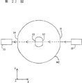
図1は、本発明の第1実施形態にかかる反射屈折結像光学系を備えた投影露光装置の全体構成を概略的に示す。なお、図1において、投影光学系を構成する反射屈折結像光学系8の光軸AXに平行にZ軸を、光軸AXに垂直な面内において図1の紙面に平行にX軸を、紙面に垂直にY軸を設定している。
図示の投影露光装置は、紫外領域の照明光を供給するための光源として、たとえばF2レーザ(発振中心波長157.6nm)を備えている。光源1から射出された光は、照明光学系2を介して、所定のパターンが形成されたマスク3を均一に照明する。
なお、光源1から照明光学系2までの光路には、必要に応じて光路を偏向するための1つまたは複数の折り曲げミラーが配置される。また、光源1と投影露光装置本体とが別体である場合には、光源1からのF2レーザ光の向きを常に投影露光装置本体へ向ける自動追尾ユニットや、光源1からのF2レーザ光の光束断面形状を所定のサイズ・形状に整形するための整形光学系、光量調整部などの光学系が配置される。また、照明光学系2は、例えばフライアイレンズや内面反射型インテグレータからなり所定のサイズ・形状の面光源を形成するオプティカルインテグレータや、マスク3上での照明領域のサイズ・形状を規定するための視野絞り、この視野絞りの像をマスク上へ投影する視野絞り結像光学系などの光学系を有する。さらに、光源1と照明光学系2との間の光路はケーシング(不図示)で密封されており、光源1から照明光学系2中の最もマスク側の光学部材までの空間は、露光光の吸収率が低い気体であるヘリウムガスや窒素などの不活性ガスで置換されている。
マスク3は、マスクホルダ4を介して、マスクステージ5上においてXY平面に平行に保持されている。マスク3には転写すべきパターンが形成されており、パターン領域全体のうちY方向に沿って長辺を有し且つX方向に沿って短辺を有する矩形状(スリット状)のパターン領域が照明される。
マスクステージ5は、図示を省略した駆動系の作用により、マスク面(すなわちXY平面)に沿って二次元的に移動可能であり、その位置座標はマスク移動鏡6を用いた干渉計7によって計測され且つ位置制御されるように構成されている。
マスク3に形成されたパターンからの光は、反射屈折型の投影光学系8を介して、感光性基板であるウエハ9上にマスクパターン像を形成する。ウエハ9は、ウエハホルダ10を介して、ウエハステージ11上においてXY平面に平行に保持されている。そして、マスク3上での矩形状の照明領域に光学的に対応するように、ウエハ9上ではY方向に沿って長辺を有し且つX方向に沿って短辺を有する矩形状の露光領域にパターン像が形成される。
ウエハステージ11は、図示を省略した駆動系の作用によりウエハ面(すなわちXY平面)に沿って二次元的に移動可能であり、その位置座標はウエハ移動鏡12を用いた干渉計13によって計測され且つ位置制御されるように構成されている。
また、図示の投影露光装置では、投影光学系8を構成する光学部材のうち最もマスク側に配置された光学部材(各実施例ではレンズL11)と最もウエハ側に配置された光学部材(各実施例では副鏡)との間で投影光学系8の内部が気密状態を保つように構成され、投影光学系8の内部の気体はヘリウムガスや窒素などの不活性ガスで置換されている。
さらに、照明光学系2と投影光学系8との間の狭い光路には、マスク3およびマスクステージ5などが配置されているが、マスク3およびマスクステージ5などを密封包囲するケーシング(不図示)の内部に窒素やヘリウムガスなどの不活性ガスが充填されている。
また、投影光学系8とウエハ9との間の狭い光路には、ウエハ9およびウエハステージ11などが配置されているが、ウエハ9およびウエハステージ11などを密封包囲するケーシング(不図示)の内部に窒素やヘリウムガスなどの不活性ガスが充填されている。
このように、光源1からウエハ9までの光路の全体に亘って、露光光がほとんど吸収されることのない雰囲気が形成されている。
上述したように、投影光学系8によって規定されるマスク3上の視野領域(照明領域)およびウエハ9上の投影領域(露光領域)は、X方向に沿って短辺を有する矩形状である。したがって、駆動系および干渉計(7、13)などを用いてマスク3およびウエハ9の位置制御を行いながら、矩形状の露光領域および照明領域の短辺方向すなわちX方向に沿ってマスクステージ5とウエハステージ11とを、ひいてはマスク3とウエハ9とを同期的に移動(走査)させることにより、ウエハ9上には露光領域の長辺に等しい幅を有し且つウエハ9の走査量(移動量)に応じた長さを有する領域に対してマスクパターンが走査露光される。
本実施形態の反射屈折結像光学系からなる投影光学系8は、以下で具体的に説明する実施例に対応する図2、4、6、8を参照して説明すると、マスク3のパターンの一次像(中間像)Iを形成するための第1結像光学系K1と、一次像Iからの光に基づいてマスクパターンの二次像を縮小倍率で感光性基板であるウエハ9上に形成するための第2結像光学系K2とから構成されている。
第1結像光学系K1は、マスク側から順に、正の屈折力を有する第1レンズ群G1と、開口絞りSと、正の屈折力を有する第2レンズ群G2とから構成されている。
第2結像光学系K2は、マスク側から順に、ウエハ側に凹面を向けた表面反射面R1を有し且つ中央に開口部を有する主鏡M1と、レンズ成分L2と、そのウエハ側のレンズ面上に設けられ且つ中央に開口部を有する反射面R2を備えた副鏡M2とから構成されている。すなわち、別の観点によれば、副鏡M2とレンズ成分L2とは裏面反射鏡を構成し、レンズ成分L2は裏面反射鏡の屈折部(屈折部材)を構成している。
なお、投影光学系8を構成するすべての光学要素(G1、G2、M1、M2)は単一の光軸AXに沿って配置されている。また、主鏡M1は一次像Iの形成位置の近傍に配置され、副鏡M2はウエハ9に近接して配置されている。
こうして、本実施形態では、マスク3のパターンからの光が、第1結像光学系K1を介して、マスクパターンの一次像(中間像)Iを形成する。一次像Iからの光は、主鏡M1の中央開口部およびレンズ成分L2を介して副鏡M2で反射され、副鏡M2で反射された光はレンズ成分L2を介して主鏡M1で反射される。主鏡M1で反射された光は、レンズ成分L2および副鏡M2の中央開口部を介してウエハ9面上にマスクパターンの二次像を縮小倍率で形成する。
本実施形態において、投影光学系8を構成するすべての屈折光学部材(レンズ成分)には蛍石(CaF2結晶)を使用している。また、露光光であるF2レーザ光の発振中心波長は157.6nmであり、157.6nm付近ではCaF2の屈折率は、+1pmの波長変化あたり−2.4×10⁻⁶の割合で変化し、−1pmの波長変化あたり+2.4×10⁻⁶の割合で変化する。
したがって、中心波長157.6nmに対するCaF2の屈折率は1.5600000である。そして、以下に説明する第1実施例および第2実施例において、157.6nm+10pm=157.61nmに対するCaF2の屈折率は1.5599760であり、157.6nm−10pm=157.59nmに対するCaF2の屈折率は1.5600240である。また、以下の第3実施例および第4実施例において、157.6nm+2pm=157.602nmに対するCaF2の屈折率は1.5599952であり、157.6nm−2pm=157.598nmに対するCaF2の屈折率は1.5600048である。
また、以下に説明する各実施例において、非球面は、光軸に垂直な方向の高さをyとし、非球面の頂点における接平面から高さyにおける非球面上の位置までの光軸に沿った距離(サグ量)をzとし、頂点曲率半径をrとし、円錐係数をκとし、n次の非球面係数をCn としたとき、以下の数式(a)で表される。
z=(y2/r)/〔1+{1−(1+κ)・y2/r2}1/2〕
+C4・y4+C6・y6+C8・y8+C10・y10
+C12・y12+C14・y14 …(a)
各実施例において、非球面形状に形成されたレンズ面には面番号の右側に*印を付している。
〔第1実施例〕
図2は、第1実施例にかかる反射屈折結像光学系(投影光学系)のレンズ構成を示す図である。第1実施例では、波長幅が157.6nm±10pmの露光光に対して色収差を含む諸収差が補正された投影光学系に本発明を適用している。
図2の反射屈折結像光学系において、第1レンズ群G1は、マスク側から順に、マスク側に非球面形状の凸面を向けた正メニスカスレンズL11と、マスク側に非球面形状の凸面を向けた正メニスカスレンズL12と、ウエハ側に非球面形状の凹面を向けた正メニスカスレンズL13とから構成されている。
また、第2レンズ群G2は、マスク側から順に、マスク側の面が非球面形状に形成された両凹レンズL21と、マスク側の面が非球面形状に形成された両凸レンズL22と、ウエハ側に非球面形状の凸面を向けた正メニスカスレンズL23と、ウエハ側に非球面形状の凹面を向けた正メニスカスレンズL24とから構成されている。
さらに、裏面反射鏡(M2、L2)の屈折部を構成するレンズ成分L2は、マスク側に非球面形状の凹面を向けた負メニスカスレンズ状に形成されている。また、副鏡M2の反射面R2は、マスク側に凹面を向けた形状に形成されている。
次の表1に、第1実施例の反射屈折結像光学系の諸元の値を掲げる。表1において、λは露光光の中心波長を、βは投影倍率を、NAは像側開口数を、φはウエハ上でのイメージサークルの直径をそれぞれ表している。また、面番号は物体面であるマスク面から像面であるウエハ面への光線の進行する方向に沿ったマスク側からの面の順序を、rは各面の曲率半径(非球面の場合には頂点曲率半径:mm)を、dは各面の軸上間隔すなわち面間隔(mm)を、nは中心波長に対する屈折率をそれぞれ示している。
なお、面間隔dは、反射される度にその符号を変えるものとする。したがって、面間隔dの符号は、裏面反射面R2から表面反射面R1までの光路中では負とし、その他の光路中では正としている。そして、光線の入射方向にかかわらずマスク側に向かって凸面の曲率半径を正とし、凹面の曲率半径を負としている。なお、以下の第2〜第4実施例においても、第1実施例と同様の符号を用いる。
【表1】
(主要諸元)
λ=157.6nm
β=0.2500
NA=0.75
φ=16.4mm
(光学部材諸元)
面番号 r d n
(マスク面) 201.4588
1* 199.4801 23.6189 1.5600000(レンズL11)
2 1933.2675 269.2901
3* 248.9462 38.4449 1.5600000(レンズL12)
4 1002.9474 19.1120
5 109.3351 28.6306 1.5600000(レンズL13)
6* 143.4010 21.0000
7 ∞ 35.4787 (開口絞りS)
8* -1979.6477 27.8589 1.5600000(レンズL21)
9 215.9777 13.6424
10* 838.3980 20.3225 1.5600000(レンズL22)
11 -252.7298 143.5573
12 -475.0282 25.5347 1.5600000(レンズL23)
13* -98.4914 12.5880
14 174.9476 50.0000 1.5600000(レンズL24)
15* 249.0942 370.2800
16* -965.4479 42.8265 1.5600000(レンズ成分L2)
17 -8820.5445 -42.8265 1.5600000(裏面反射面R2)
18* -965.4479 -223.7172
19 346.8643 223.7172 1.5600000(表面反射面R1)
20* -965.4479 42.8265 1.5600000(レンズ成分L2)
21 -8820.5445 10.0000
(ウエハ面)
(非球面データ)
r κ C4
1面 199.4801 0.00000 -9.61173×10⁻⁹
C6 C8 C10
-2.14569×10⁻¹³ 7.59160×10⁻¹⁸ -5.90665×10⁻²²
C12 C14
0.00000 0.00000
r κ C4
3面 248.9462 0.00000 -1.55615×10⁻⁷
C6 C8 C10
-4.68023×10⁻¹² 3.66473×10⁻¹⁸ 2.76851×10⁻²¹
C12 C14
4.46701×10⁻²⁵ 0.00000
r κ C4
6面 143.4010 0.00000 -1.49247×10⁻⁷
C6 C8 C10
2.48237×10⁻¹² 1.10343×10⁻¹⁵ -6.65598×10⁻²⁰
C12 C14
-2.15738×10⁻²⁴ 0.00000
r κ C4
8面 -1979.6477 0.00000 -9.40388×10⁻⁸
C6 C8 C10
-4.01544×10⁻¹² -6.89483×10⁻¹⁷ 1.70469×10⁻²⁰
C12 C14
-6.15241×10⁻²⁴ 0.00000
r κ C4
10面 838.3980 0.00000 1.88036×10⁻⁸
C6 C8 C10
-1.59516×10⁻¹² -3.15148×10⁻¹⁶ -2.20945×10⁻²⁰
C12 C14
0.00000 0.00000
r κ C4
13面 -98.4914 0.00000 1.67077×10⁻⁷
C6 C8 C10
-2.42295×10⁻¹² 1.58927×10⁻¹⁵ -1.11815×10⁻¹⁹
C12 C14
1.37831×10⁻²³ 0.00000
r κ C4
15面 249.0942 0.00000 -1.42562×10⁻⁷
C6 C8 C10
2.11000×10⁻¹¹ -3.82147×10⁻¹⁵ 2.44894×10⁻¹⁹
C12 C14
0.00000 0.00000
r κ C4
16面 -965.4479 17.065794 7.65400×10⁻⁹
18面 C6 C8 C10
20面 -7.96595×10⁻¹⁵ -8.95740×10⁻¹⁹ 6.26276×10⁻²³
C12 C14
-1.26805×10⁻²⁷ 1.50073×10⁻³²
(条件式対応値)
D=300.000mm
R=−965.448mm
β1=0.6249
β2=0.4000
(1)D/|R|=0.3107
(2)|β1/β2|=1.5622
図3は、第1実施例における横収差を示す図である。
収差図において、Yは像高を、実線は中心波長157.6nmを、破線は157.6nm+10pm=157.61nmを、一点鎖線は157.6nm−10pm=157.59nmをそれぞれ示している。
収差図から明らかなように、第1実施例では、波長幅が157.6nm±10pmの露光光に対して色収差が良好に補正されていることがわかる。また、図示を省略したが、球面収差、非点収差、歪曲収差などの諸収差も良好に補正されていることが確認されている。
以上のように、第1実施例の反射屈折結像光学系では、中心波長が157.6nmのF2レーザ光に対して、少ないレンズ枚数で、主鏡M1を大型化することなく、0.75の像側NAを確保するとともに、ウエハ上で16.4mmのイメージサークルを確保することができる。したがって、第1実施例の反射屈折結像光学系を投影露光装置に適用した場合、0.1μm以下の高解像を達成することができる。また、第1実施例では、露光領域を直径16.4mmのイメージサークル内で15mm×6mmの矩形状に設定することができる。ここで、2回のスキャン露光を用いた継ぎ露光を行うことにより、例えば30mm×40mmの領域にマスクパターンを転写することができる。
〔第2実施例〕
図4は、第2実施例にかかる反射屈折結像光学系(投影光学系)のレンズ構成を示す図である。第2実施例では第1実施例と同様に、波長幅が157.6nm±10pmの露光光に対して色収差を含む諸収差が補正された投影光学系に本発明を適用している。
図4の反射屈折結像光学系において、第1レンズ群G1は、マスク側から順に、マスク側の面が非球面形状に形成された両凸レンズL11と、マスク側に非球面形状の凸面を向けた正メニスカスレンズL12と、ウエハ側に非球面形状の凹面を向けた正メニスカスレンズL13とから構成されている。
また、第2レンズ群G2は、マスク側から順に、マスク側の面が非球面形状に形成された両凹レンズL21と、マスク側の面が非球面形状に形成された両凸レンズL22と、ウエハ側に非球面形状の凸面を向けた正メニスカスレンズL23と、ウエハ側に非球面形状の凹面を向けた正メニスカスレンズL24とから構成されている。
さらに、裏面反射鏡(M2、L2)の屈折部を構成するレンズ成分L2は、マスク側に非球面形状の凹面を向けた負メニスカスレンズ状に形成されている。また、副鏡M2の反射面R2は、マスク側に凹面を向けた形状に形成されている。
次の表2に、第2実施例の反射屈折結像光学系の諸元の値を掲げる。表2において、λは露光光の中心波長を、βは投影倍率を、NAは像側開口数を、φはウエハ上でのイメージサークルの直径をそれぞれ表している。また、面番号は物体面であるマスク面から像面であるウエハ面への光線の進行する方向に沿ったマスク側からの面の順序を、rは各面の曲率半径(非球面の場合には頂点曲率半径:mm)を、dは各面の軸上間隔すなわち面間隔(mm)を、nは中心波長に対する屈折率をそれぞれ示している。
なお、面間隔dは、反射される度にその符号を変えるものとする。したがって、面間隔dの符号は、裏面反射面R2から表面反射面R1までの光路中では負とし、その他の光路中では正としている。そして、光線の入射方向にかかわらずマスク側に向かって凸面の曲率半径を正とし、凹面の曲率半径を負としている。
【表2】
(主要諸元)
λ=157.6nm
β=0.1667
NA=0.75
φ=16.4mm
(光学部材諸元)
面番号 r d n
(マスク面) 242.1618
1* 348.3645 20.3520 1.5600000(レンズL11)
2 -3554.8348 467.3225
3* 239.8908 34.8496 1.5600000(レンズL12)
4 1352.4428 15.8591
5 102.0339 25.6961 1.5600000(レンズL13)
6* 135.8731 15.0000
7 ∞ 33.0010 (開口絞りS)
8* -1646.0094 15.0000 1.5600000(レンズL21)
9 162.8326 12.6590
10* 3782.8629 28.4575 1.5600000(レンズL22)
11 -167.4700 138.8995
12 -667.4486 23.1320 1.5600000(レンズL23)
13* -98.3804 12.2947
14 238.6417 40.0000 1.5600000(レンズL24)
15* 450.8009 367.0741
16* -1060.8317 35.7201 1.5600000(レンズ成分L2)
17 -12438.4006 -35.7201 1.5600000(裏面反射面R2)
18* -1060.8317 -225.9787
19 345.5693 225.9787 1.5600000(表面反射面R1)
20* -1060.8317 35.7201 1.5600000(レンズ成分L2)
21 -12438.4006 10.3738
(ウエハ面)
(非球面データ)
r κ C4
1面 348.3645 0.00000 -1.99908×10⁻⁹
C6 C8 C10
-2.61608×10⁻¹⁴ 1.74287×10⁻¹⁸ -8.67060×10⁻²³
C12 C14
0.00000 0.00000
r κ C4
3面 239.8908 0.00000 -1.46594×10⁻⁷
C6 C8 C10
-3.72404×10⁻¹² 7.48186×10⁻¹⁷ 7.76854×10⁻²¹
C12 C14
-9.84338×10⁻²⁶ 0.00000
r κ C4
6面 135.8731 0.00000 -1.31223×10⁻⁷
C6 C8 C10
4.10629×10⁻¹² 1.24814×10⁻¹⁵ -6.18827×10⁻²⁰
C12 C14
-2.87148×10⁻²⁴ 0.00000
r κ C4
8面 -1646.0094 0.00000 -9.95674×10⁻⁸
C6 C8 C10
-1.74464×10⁻¹² 4.69373×10⁻¹⁶ -1.31864×10⁻²⁰
C12 C14
-5.68871×10⁻²⁴ 0.00000
r κ C4
10面 3782.8629 0.00000 1.43307×10⁻⁸
C6 C8 C10
-1.22504×10⁻¹³ -4.09091×10⁻¹⁶ -1.15700×10⁻²⁰
C12 C14
0.00000 0.00000
r κ C4
13面 -98.3804 0.00000 1.88420×10⁻⁷
C6 C8 C10
-6.07613×10⁻¹² 2.32619×10⁻¹⁵ -2.09690×10⁻¹⁹
C12 C14
2.06538×10⁻²³ 0.00000
r κ C4
15面 450.8009 0.00000 -1.45913×10⁻⁷
C6 C8 C10
2.29629×10⁻¹¹ -4.70746×10⁻¹⁵ 3.43229×10⁻¹⁹
C12 C14
0.00000 0.00000
r κ C4
16面 -1060.8317 18.256260 7.10920×10⁻⁹
18面 C6 C8 C10
20面 -2.92379×10⁻¹⁴ -4.67533×10⁻¹⁹ 4.87403×10⁻²³
C12 C14
-1.11194×10⁻²⁷ 1.25627×10⁻³²
(条件式対応値)
D=291.067mm
R=−1060.832mm
β1=0.4229
β2=0.3941
(1)D/|R|=0.2744
(2)|β1/β2|=1.0731
図5は、第2実施例における横収差を示す図である。
収差図において、Yは像高を、実線は中心波長157.6nmを、破線は157.6nm+10pm=157.61nmを、一点鎖線は157.6nm−10pm=157.59nmをそれぞれ示している。
収差図から明らかなように、第2実施例においても第1実施例と同様に、波長幅が157.6nm±10pmの露光光に対して色収差が良好に補正されていることがわかる。また、図示を省略したが、球面収差、非点収差、歪曲収差などの諸収差も良好に補正されていることが確認されている。
以上のように、第2実施例の反射屈折結像光学系においても第1実施例と同様に、中心波長が157.6nmのF2レーザ光に対して、少ないレンズ枚数で、主鏡M1を大型化することなく、0.75の像側NAを確保するとともに、ウエハ上で16.4mmのイメージサークルを確保することができる。したがって、第2実施例の反射屈折結像光学系を投影露光装置に適用した場合、0.1μm以下の高解像を達成することができる。また、第1実施例と同様に第2実施例では、露光領域を直径16.4mmのイメージサークル内で15mm×6mmの矩形状に設定することができる。ここで、2回のスキャン露光を用いた継ぎ露光を行うことにより、例えば30mm×40mmの領域にマスクパターンを転写することができる。
〔第3実施例〕
図6は、第3実施例にかかる反射屈折結像光学系(投影光学系)のレンズ構成を示す図である。第3実施例では、第1実施例および第2実施例とは異なり、波長幅が157.6nm±2pmの露光光に対して色収差を含む諸収差が補正された投影光学系に本発明を適用している。
図6の反射屈折結像光学系において、第1レンズ群G1は、マスク側から順に、マスク側の面が非球面形状に形成された両凸レンズL11と、マスク側の面が非球面形状に形成された両凸レンズL12と、ウエハ側に非球面形状の凹面を向けた正メニスカスレンズL13とから構成されている。
また、第2レンズ群G2は、マスク側から順に、マスク側の面が非球面形状に形成された両凹レンズL21と、マスク側の面が非球面形状に形成された両凸レンズL22と、ウエハ側に非球面形状の凸面を向けた正メニスカスレンズL23と、ウエハ側に非球面形状の凹面を向けた正メニスカスレンズL24と、ウエハ側の面が非球面形状に形成された両凹レンズL25とから構成されている。
さらに、裏面反射鏡(M2、L2)の屈折部を構成するレンズ成分L2は、マスク側に非球面形状の凹面を向けた負メニスカスレンズ状に形成されている。また、副鏡M2の反射面R2は、マスク側に凹面を向けた形状に形成されている。
次の表3に、第3実施例の反射屈折結像光学系の諸元の値を掲げる。表3において、λは露光光の中心波長を、βは投影倍率を、NAは像側開口数を、φはウエハ上でのイメージサークルの直径をそれぞれ表している。また、面番号は物体面であるマスク面から像面であるウエハ面への光線の進行する方向に沿ったマスク側からの面の順序を、rは各面の曲率半径(非球面の場合には頂点曲率半径:mm)を、dは各面の軸上間隔すなわち面間隔(mm)を、nは中心波長に対する屈折率をそれぞれ示している。
なお、面間隔dは、反射される度にその符号を変えるものとする。したがって、面間隔dの符号は、裏面反射面R2から表面反射面R1までの光路中では負とし、その他の光路中では正としている。そして、光線の入射方向にかかわらずマスク側に向かって凸面の曲率半径を正とし、凹面の曲率半径を負としている。
【表3】
(主要諸元)
λ=157.6nm
β=0.2500
NA=0.75
φ=26.4mm
(光学部材諸元)
面番号 r d n
(マスク面) 212.4984
1* 271.1840 55.1190 1.5600000(レンズL11)
2 -1813.8535 292.8580
3* 311.8049 27.9307 1.5600000(レンズL12)
4 -5255.1075 1.0000
5 152.8546 25.0365 1.5600000(レンズL13)
6* 216.9976 40.6000
7 ∞ 11.5638 (開口絞りS)
8* -6722.7061 18.6098 1.5600000(レンズL21)
9 161.3409 42.0666
10* 423.2188 60.0000 1.5600000(レンズL22)
11 -178.2896 146.6461
12 -744.0670 54.2587 1.5600000(レンズL23)
13* -142.1914 16.5488
14 278.3048 50.6377 1.5600000(レンズL24)
15* 2290.2523 63.5676
16 -4911.6877 35.3230 1.5600000(レンズL25)
17* 7183.0248 266.3990
18* -951.7953 30.2109 1.5600000(レンズ成分L2)
19 -4911.6877 -30.2109 1.5600000(裏面反射面R2)
20* -951.7953 -226.3990
21 344.7892 226.3990 1.5600000(表面反射面R1)
22* -951.7953 30.2109 1.5600000(レンズ成分L2)
23 -4911.6877 10.0000
(ウエハ面)
(非球面データ)
r κ C4
1面 271.1840 0.00000 -4.13100×10⁻⁹
C6 C8 C10
-4.86836×10⁻¹⁴ 5.18033×10⁻¹⁹ -2.34891×10⁻²³
C12 C14
0.00000 0.00000
r κ C4
3面 311.8049 0.00000 -1.61517×10⁻⁷
C6 C8 C10
-1.25518×10⁻¹² 1.97882×10⁻¹⁶ 5.26274×10⁻²¹
C12 C14
-6.29521×10⁻²⁵ 0.00000
r κ C4
6面 216.9976 0.00000 -1.23619×10⁻⁷
C6 C8 C10
3.70374×10⁻¹² 6.92531×10⁻¹⁶ -5.14929×10⁻²⁰
C12 C14
9.15839×10⁻²⁶ 0.00000
r κ C4
8面 -6722.7061 0.00000 -7.87222×10⁻⁸
C6 C8 C10
-5.25993×10⁻¹² 6.65324×10⁻¹⁷ -2.77521×10⁻²¹
C12 C14
-2.07292×10⁻²⁴ 0.00000
r κ C4
10面 423.2188 0.00000 2.83109×10⁻⁸
C6 C8 C10
1.39256×10⁻¹² -1.14067×10⁻¹⁶ 1.60286×10⁻²²
C12 C14
0.00000 0.00000
r κ C4
13面 -142.1914 0.00000 6.81342×10⁻⁸
C6 C8 C10
-4.96671×10⁻¹³ 2.11714×10⁻¹⁶ -9.23870×10⁻²¹
C12 C14
7.74512×10⁻²⁵ 0.00000
r κ C4
15面 2290.2523 0.00000 -3.65549×10⁻⁸
C6 C8 C10
3.60552×10⁻¹² -3.34833×10⁻¹⁶ -5.30167×10⁻²⁰
C12 C14
0.00000 0.00000
r κ C4
17面 7183.0248 0.00000 -2.46580×10⁻⁸
C6 C8 C10
1.69228×10⁻¹² 1.62175×10⁻¹⁶ -2.27785×10⁻¹⁹
C12 C14
5.70974×10⁻³⁵ 0.00000
r κ C4
18面 -951.7953 16.818076 8.20688×10⁻⁹
20面 C6 C8 C10
22面 -2.48038×10⁻¹⁴ -8.45982×10⁻¹⁹ 8.17477×10⁻²³
C12 C14
-1.96463×10⁻²⁷ 2.43799×10⁻³²
(条件式対応値)
D=292.019mm
R=−951.795mm
β1=0.6083
β2=0.4110
(1)D/|R|=0.3068
(2)|β1/β2|=1.4799
図7は、第3実施例における横収差を示す図である。
収差図において、Yは像高を、実線は中心波長157.6nmを、破線は157.6nm+2pm=157.602nmを、一点鎖線は157.6nm−2pm=157.598nmをそれぞれ示している。
収差図から明らかなように、第3実施例では、波長幅が157.6nm±2pmの露光光に対して色収差が良好に補正されていることがわかる。また、図示を省略したが、球面収差、非点収差、歪曲収差などの諸収差も良好に補正されていることが確認されている。
以上のように、第3実施例の反射屈折結像光学系では、中心波長が157.6nmのF2レーザ光に対して、少ないレンズ枚数で、主鏡M1を大型化することなく、0.75の像側NAを確保するとともに、ウエハ上で26.4mmのイメージサークルを確保することができる。したがって、第3実施例の反射屈折結像光学系を投影露光装置に適用した場合、0.1μm以下の高解像を達成することができる。また、露光領域をたとえば25mm×8mmの矩形状に設定し、1回のスキャン露光により25mm×33mmの領域にマスクパターンを転写することができる。なお、第1及び第2実施例と同様に複数回のスキャン露光を用いた継ぎ露光を行っても良い。
〔第4実施例〕
図8は、第4実施例にかかる反射屈折結像光学系(投影光学系)のレンズ構成を示す図である。第4実施例では、第3実施例と同様に、波長幅が157.6nm±2pmの露光光に対して色収差を含む諸収差が補正された投影光学系に本発明を適用している。
図8の反射屈折結像光学系において、第1レンズ群G1は、マスク側から順に、マスク側に非球面形状の凹面を向けた正メニスカスレンズL11と、マスク側に非球面形状の凸面を向けた正メニスカスレンズL12と、マスク側に非球面形状の凹面を向けた負メニスカスレンズL13と、マスク側に非球面形状の凸面を向けた正メニスカスレンズL14とから構成されている。
また、第2レンズ群G2は、マスク側から順に、マスク側に非球面形状の凹面を向けた負メニスカスレンズL21と、マスク側に非球面形状の凹面を向けた正メニスカスレンズL22と、マスク側の面が非球面形状に形成された両凸レンズL23と、ウエハ側の面が非球面形状に形成された両凸レンズL24とから構成されている。
さらに、裏面反射鏡(M2、L2)の屈折部を構成するレンズ成分L2は、マスク側に非球面形状の凹面を向けた両凹レンズ状に形成されている。また、副鏡M2の反射面R2は、マスク側に凸面を向けた形状に形成されている。
次の表4に、第4実施例の反射屈折結像光学系の諸元の値を掲げる。表4において、λは露光光の中心波長を、βは投影倍率を、NAは像側開口数を、φはウエハ上でのイメージサークルの直径をそれぞれ表している。また、面番号は物体面であるマスク面から像面であるウエハ面への光線の進行する方向に沿ったマスク側からの面の順序を、rは各面の曲率半径(非球面の場合には頂点曲率半径:mm)を、dは各面の軸上間隔すなわち面間隔(mm)を、nは中心波長に対する屈折率をそれぞれ示している。
なお、面間隔dは、反射される度にその符号を変えるものとする。したがって、面間隔dの符号は、裏面反射面R2から表面反射面R1までの光路中では負とし、その他の光路中では正としている。そして、光線の入射方向にかかわらずマスク側に向かって凸面の曲率半径を正とし、凹面の曲率半径を負としている。
【表4】
(主要諸元)
λ=157.6nm
β=0.2500
NA=0.75
φ=26.4mm
(光学部材諸元)
面番号 r d n
(マスク面) 90.0000
1* -1040.1889 16.8787 1.5600000(レンズL11)
2 -284.5252 441.0860
3* 248.9993 31.6042 1.5600000(レンズL12)
4 1868.1161 86.0264
5* -256.4757 15.0000 1.5600000(レンズL13)
6 -1079.5886 1.0001
7* 160.4237 39.0505 1.5600000(レンズL14)
8 1268.4783 3.7000
9 ∞ 70.0471 (開口絞りS)
10* -129.2757 15.0000 1.5600000(レンズL21)
11 -277.5549 78.6066
12* -1494.7189 45.0000 1.5600000(レンズL22)
13 -238.2212 91.8347
14* 365.9254 18.9298 1.5600000(レンズL23)
15 -701.6534 129.1513
16 4243.7172 16.9695 1.5600000(レンズL24)
17* -216.4772 290.1728
18* -2125.3388 59.9425 1.5600000(レンズ成分L2)
19 5996.9618 -59.9425 1.5600000(裏面反射面R2)
20* -2125.3388 -230.3293
21 350.1412 230.3293 1.5600000(表面反射面R1)
22* -2125.3388 59.9425 1.5600000(レンズ成分L2)
23 5996.9618 10.0000
(ウエハ面)
(非球面データ)
r κ C4
1面 -1040.1889 0.00000 8.50114×10⁻⁹
C6 C8 C10
9.40854×10⁻¹⁴ 3.85092×10⁻¹⁸ -5.46679×10⁻²²
C12 C14
0.00000 0.00000
r κ C4
3面 248.9993 0.00000 -1.42904×10⁻¹⁰
C6 C8 C10
6.60616×10⁻¹⁴ 3.65786×10⁻¹⁸ -1.09842×10⁻²²
C12 C14
4.97484×10⁻²⁷ 0.00000
r κ C4
5面 -256.4757 0.00000 5.80903×10⁻⁹
C6 C8 C10
1.21604×10⁻¹³ 1.20391×10⁻¹⁷ 1.45440×10⁻²²
C12 C14
6.87071×10⁻²⁷ 0.00000
r κ C4
7面 160.4237 0.00000 -6.83384×10⁻⁹
C6 C8 C10
5.93636×10⁻¹³ 6.46685×10⁻¹⁸ 5.93586×10⁻²²
C12 C14
9.08641×10⁻²⁶ 0.00000
r κ C4
10面 -129.2757 0.00000 -1.19158×10⁻⁸
C6 C8 C10
5.20234×10⁻¹² 1.68410×10⁻¹⁶ 6.16591×10⁻²¹
C12 C14
-3.28458×10⁻²⁵ 0.00000
r κ C4
12面 -1494.7189 0.00000 3.04547×10⁻⁸
C6 C8 C10
-2.21766×10⁻¹² 1.10527×10⁻¹⁶ -3.25713×10⁻²¹
C12 C14
1.29445×10⁻²⁵ 0.00000
r κ C4
14面 365.9254 0.00000 -3.76800×10⁻⁸
C6 C8 C10
1.05958×10⁻¹³ -2.08225×10⁻¹⁷ 1.53887×10⁻²¹
C12 C14
-1.62147×10⁻²⁵ 0.00000
r κ C4
17面 -216.4772 0.00000 1.07160×10⁻⁸
C6 C8 C10
-1.20868×10⁻¹³ -2.81385×10⁻¹⁸ 2.81683×10⁻²¹
C12 C14
0.00000 0.00000
r κ C4
18面 -2125.3388 91.723346 5.77862×10⁻¹⁰
20面 C6 C8 C10
22面 -2.56941×10⁻¹⁴ 1.81191×10⁻¹⁸ -4.17947×10⁻²³
C12 C14
1.10317×10⁻²⁷ -1.11337×10⁻³²
(条件式対応値)
D=290.300mm
R=−2125.339mm
β1=0.5350
β2=0.4673
(1)D/|R|=0.1366
(2)|β1/β2|=1.1449
図9は、第4実施例における横収差を示す図である。
収差図において、Yは像高を、実線は中心波長157.6nmを、破線は157.6nm+2pm=157.602nmを、一点鎖線は157.6nm−2pm=157.598nmをそれぞれ示している。
収差図から明らかなように、第4実施例では第3実施例と同様に、波長幅が157.6nm±2pmの露光光に対して色収差が良好に補正されていることがわかる。また、図示を省略したが、球面収差、非点収差、歪曲収差などの諸収差も良好に補正されていることが確認されている。
以上のように、第4実施例の反射屈折結像光学系においても第3実施例と同様に、中心波長が157.6nmのF2レーザ光に対して、少ないレンズ枚数で、主鏡M1を大型化することなく、0.75の像側NAを確保するとともに、ウエハ上で26.4mmのイメージサークルを確保することができる。したがって、第4実施例の反射屈折結像光学系を投影露光装置に適用した場合、0.1μm以下の高解像を達成することができる。また、第3実施例と同様に、露光領域をたとえば25mm×8mmの矩形状に設定し、1回のスキャン露光により25mm×33mmの領域にマスクパターンを転写することができる。なお、第1及び第2実施例と同様に複数回のスキャン露光を用いた継ぎ露光を行っても良い。
(第2実施形態)
以下、本発明の第2実施形態に係る反射屈折結像光学系を説明する。
第2実施形態に係る反射屈折結像光学系を備えた投影露光装置の全体構成については、図1と同様であり第1実施形態の説明をそのまま引用できる。よって、ここでは重複する説明を省略する。
本実施形態の反射屈折結像光学系からなる投影光学系8は、以下で具体的に説明する実施例に対応する図10、12を参照して説明すると、マスク3のパターンの一次像(中間像)を形成するための第1結像光学系K1と、一次像からの光に基づいてマスクパターンの二次像(最終像)を縮小倍率で感光性基板であるウエハ9上に形成するための第2結像光学系K2とから構成されている。第1結像光学系K1は、マスク側から順に、正の屈折力を有する第1レンズ群G1と、開口絞りSと、正の屈折力を有する第2レンズ群G2とから構成されている。
第2結像光学系K2は、マスク側から順に、ウエハ側に凹面を向けた表面反射面R1を有し且つ中央に開口部(光透過部)を有する主鏡M1と、レンズ成分L2と、中央に開口部(光透過部)を有する反射面R2を備えた副鏡M2とから構成されている。
なお、投影光学系8を構成するすべての光学要素(G1,G2,M1,M2,L2)は単一の光軸AXに沿って配置されている。また、主鏡M1は一次像の形成位置の近傍に配置され、副鏡M2はウエハ9に近接して配置されている。
こうして、本実施形態では、マスク3のパターンからの光が、第1結像光学系K1を介して、マスクパターンの一次像(中問像)を形成する。一次像からの光は、主鏡M1の中央開口部及びレンズ成分L2を介して副鏡M2で反射され、副鏡M2で反射された光はレンズ成分L2を介して主鏡M1で反射される。主鏡M1で反射された光は、レンズ成分L2及び副鏡M2の中央開口部を介してウエハ9面上にマスクパターンの二次像を縮小倍率で形成する。
本実施形態において、投影光学系8を構成するすべての屈折光学部材(レンズ成分)には蛍石(CaF2結晶)を使用している。また、露光光であるF2レーザ光の発振中心波長は157.6nmであり、157.6nm付近ではCaF2の屈折率は、+1pmの波長変化あたり−2.4×10⁻⁶の割合で変化し、−1pmの波長変化あたり+2.4×10⁻⁶の割合で変化する。
従って、中心波長157.6nmに対するCaF2の屈折率は1.5600000である。そして、各実施例において、157.6nm+10pm=157.61nmに対するCaF2の屈折率は1.5599760であり、157.6nm−10pm=157.59nmに対するCaF2の屈折率は1.5600240である。
また、以下に説明する各実施例において、非球面は、第1実施形態で既に説明した数式(a)にて表される。なお、以下の各実施例において、非球面形状に形成されたレンズ面には面番号の右側に*印を付している。
〔第5実施例〕
図10は、第5実施例にかかる反射屈折結像光学系(投影光学系)のレンズ構成を示す図である。第5実施例では、波長幅が157.6nm±10pmの露光光に対して色収差を含む諸収差が補正された投影光学系に本発明を適用している。図10の反射屈折結像光学系は、マスク3の中間像を形成するための屈折型の第1結像光学系K1と、前記中間像からの光に基づいてマスク3の最終像を縮小倍率でウエハ9上に形成するための反射屈折型の第2結像光学系K2とを備えている。そして、第1結像光学系K1は、マスク3側から順に、正屈折力の第1レンズ群G1と、開口絞りSと、正屈折力の第2レンズ群G2とを有し、第2結像光学系K2は、中央部に第1光通過部AP1を有する負屈折力の第1反射面R1からなる主鏡M1と、中央部に第2光通過部AP2を有する第2反射面R2からなる副鏡M2と、第1反射面R1及び第2反射面R2から離間されているウエハ側に凹面を向けた屈折面を有するレンズ成分L2とを有している。
第1レンズ群G1は、マスク側から順に、マスク側に非球面形状の凸面を向けたメニスカスレンズL11と、マスク側に非球面形状の凸面を向けた両凸レンズL12と、ウエハ側に非球面形状の凹面を向けたメニスカスレンズL13と、マスク側に非球面形状の凸面を向けたメニスカスレンズL14とから構成されている。
また、第2レンズ群G2は、マスク側から順に、マスク側に非球面形状の凸面を向けたメニスカスレンズL21と、ウエハ側に非球面形状の凸面を向けた両凸レンズL22と、ウエハ側に非球面形状の凹面を向けたメニスカスレンズL23とから構成されている。
さらに、第2結像光学系K2は、ウエハ側に非球面形状の凹面を向けた負メニスカスレンズL2を含んでいる。
また、第1結像光学系K1は、光軸AXの方向において開口絞りSとは異なる位置に配置されて光軸AX近傍の光を遮光する中心遮蔽部材Bを有する。
かかる構成において、第1結像光学系K1からの光が主鏡M1の第1光透過部AP1とレンズ成分L2とを介して第2反射面R2で反射され、第2反射面R2で反射された光がレンズ成分L2を介して第1反射面R1で反射され、第1反射面R1で反射された光がレンズ成分L2と副鏡M2の第2光通過部AP2とを介してウエハ面9上に最終像を形成する。
以下の表5に、第5実施例の反射屈折結像光学系の諸元の値を掲げる。表5において、λは露光光の中心波長を、βは投影倍率を、NAは像側開口数を、φはウエハ上でのイメージサークルの直径をそれぞれ表している。また、面番号は物体面であるマスク面から像面であるウエハ面への光線の進行する方向に沿ったマスク側からの面の順序を、rは各面の曲率半径(非球面の場合には頂点曲率半径:mm)を、dは各面の軸上問隔すなわち面間隔(mm)を、nは中心波長(λ=157.6nm)に対する屈折率をそれぞれ示している。
また、面間隔dは、反射される度にその符号を変えるものとする。従って、面間隔dの符号は、反射面R2から反射面R1までの光路中では負とし、その他の光路中では正としている。そして、光線の入射方向にかかわらずマスク側に向かって凸面の曲率半径を正とし、凹面の曲率半径を負としている。なお、以下の第6実施例において、第5実施例と同様の符号を用いる。
【表5】
(主要諸元)
λ=157.6nm±10pm
β=0.2500
NA=0.75
φ=16.4mm
Δn/Δλ=2.4×10-6(Δλ=1pm)
面番号 r d n
1* 169.7986 25.120 1.5600000
2 828.2434 248.638
3* 419.3057 17.377 1.5600000
4 -358.6668 1.000
5 99.9661 38.596 1.5600000
6* 141.0006 11.462
7* 64162.6646 15.000 1.5600000
8 156.1861 10.033
9 0.0000 115.356 (開口絞り)
10* 126.7181 39.667 1.5600000
11 140.6882 48.857
12 360.0217 32.301 1.5600000
13* -111.1630 60.049
14 168.2754 60.000 1.5600000
15* 188.7785 14.271
16 0.0000 253.659
17 1763.6223 39.730 1.5600000
18* 604.2607 12.936
19 0.0000 -12.936
20* 604.2607 -39.730 1.5600000
21 1763.6223 -213.659
22 341.6710 213.659
23 1763.6226 39.730 1.5600000
24* 604.2607 25.936
(非球面データ)
r κ C4
1面 169.7986 0.00000 -1.77640×10⁻⁸
C6 C8 C10
-3.15876×10⁻¹³ -4.58542×10⁻¹⁸ -4.33089×10⁻²²
C12 C14
0.00000 0.00000
r κ C4
3面 419.3057 0.00000 -2.26166×10⁻⁷
C6 C8 C10
6.74494×10⁻¹³ 2.78902×10⁻¹⁶ -8.28386×10⁻²¹
C12 C14
-1.96187×10⁻²⁶ 0.00000
r κ C4
6面 141.0006 0.00000 -1.79523×10⁻⁷
C6 C8 C10
3.36890×10⁻¹¹ 2.84625×10⁻¹⁵ -3.81299×10⁻¹⁹
C12 C14
4.94390×10⁻²³ 0.00000
r κ C4
7面 64162.6646 0.00000 1.11972×10⁻⁷
C6 C8 C10
-5.67876×10⁻¹² 4.12815×10⁻¹⁶ 5.65399×10⁻²⁰
C12 C14
-2.14735×10⁻²³ 0.00000
r κ C4
10面 126.7181 0.00000 -5.63527×10⁻⁸
C6 C8 C10
3.24172×10⁻¹³ -5.77177×10⁻¹⁷ 5.45422×10⁻²¹
C12 C14
0.00000 0.00000
r κ C4
13面 -111.1630 0.00000 1.28904×10⁻⁷
C6 C8 C10
2.37711×10⁻¹² 3.46806×10⁻¹⁶ -1.34551×10⁻²²
C12 C14
2.44040×10⁻²⁴ 0.00000
r κ C4
15面 188.7785 0.00000 -5.43671×10⁻⁸
C6 C8 C10
4.63484×10⁻¹² 1.53536×10⁻¹⁴ -1.26491×10⁻¹⁷
C12 C14
0.00000 0.00000
r κ C4
18面 604.2607 0.00000 -9.80093×10⁻⁹
20面 C6 C8 C10
24面 1.49653×10⁻¹⁴ 9.52668×10⁻¹⁸ -5.35859×10⁻²²
C12 C14
1.52780×10⁻²⁶ -1.91921×10⁻³¹
(条件式対応値)
(3) f1/d1=−64.0760
(4) |β1/β2|=1.5271
図11は、第5実施例における横収差を示す図である。収差図において、Yは像高を、実線は中心波長157.6nmを、破線は157.6nm+10pm=157.61nmを、一点鎖線は157.6nm−10pm=157.59nmをそれぞれ示している。収差図から明らかなように、第5実施例では、波長幅が157.6nm±10pmの露光光に対して色収差が良好に補正されていることがわかる。また、図示を省略したが、球面収差、非点収差、歪曲収差などの諸収差も良好に補正されていることが確認されている。
以上のように、第5実施例の反射屈折結像光学系では、中心波長が157.6nmのF2レーザ光に対して、少ないレンズ枚数で、主鏡M1を大型化することなく、0.75の像側NAを確保するとともに、ウエハ上で16.4mmのイメージサークルを確保することができる。従って、第5実施例の反射屈折結像光学系を投影露光装置に適用した場合、0.1μm以下の高解像を達成することができる。また、第5実施例では、露光領域を直径16.4mmイメージサークル内で15mm×6mmの矩形状に設定することができる。ここで、2回のスキャン露光を用いた継ぎ露光を行うことにより、例えば30mm×40mmの領域にマスクパターンを転写することができる。
〔第6実施例〕
図12は、第6実施例にかかる反射屈折結像光学系(投影光学系)のレンズ構成を示す図である。第6実施例では第5実施例と同様に、波長幅が157.6nm±10pmの露光光に対して色収差を含む諸収差が補正された投影光学系に本発明を適用している。
図12の反射屈折結像光学系は、マスク3の中間像を形成するための屈折型の第1結像光学系K1と、前記中間像からの光に基づいてマスク3の最終像を縮小倍率でウエハ9上に形成するための反射屈折型の第2結像光学系K2とを備えている。そして、第1結像光学系K1は、マスク3側から順に、正屈折力の第1レンズ群G1と、開口絞りSと、正屈折力の第2レンズ群G2とを有し、第2結像光学系K2は、中央部に第1光通過部AP1を有する負屈折力の第1反射面R1からなる主鏡M1と、中央部に第2光通過部AP2を有する第2反射面R2からなる副鏡M2と、第1反射面R1及び第2反射面R2から離間されているウエハ側に凹面を向けた屈折面を有するレンズ成分L2とを有している。
第1レンズ群G1は、マスク側から順に、マスク側に非球面形状の凸面を向けたメニスカスレンズL11と、マスク側に非球面形状の凸面を向けた両凸レンズL12と、ウエハ側に非球面形状の凹面を向けたメニスカスレンズL13と、マスク側に非球面形状の凸面を向けたメニスカスレンズL14とから構成されている。
また、第2レンズ群G2は、マスク側から順に、マスク側に非球面形状の凸面を向けたメニスカスレンズL21と、ウエハ側に非球面形状の凸面を向けた両凸レンズL22と、ウエハ側に非球面形状の凸面を向けたメニスカスレンズL23と、ウエハ側に非球面形状の凹面を向けたメニスカスレンズL24とから構成されている。さらに、第2結像光学系K2は、ウエハ側に非球面形状の凹面を向けた負メニスカスレンズL2を含んでいる。
また、第1結像光学系K1は、光軸AXの方向において開口絞りSとは異なる位置に配置されて光軸AX近傍の光を遮光する中心遮蔽部材Bを有する。
かかる構成において、第1結像光学系K1からの光が主鏡M1の第1光透過部AP1とレンズ成分L2とを介して第2反射面R2で反射され、第2反射面R2で反射された光がレンズ成分L2を介して第1反射面R1で反射され、第1反射面R1で反射された光がレンズ成分L2と副鏡M2の第2光通過部AP2とを介してウエハ面9上に最終像を形成する。
以下の表6に、第6実施例の反射屈折結像光学系の諸元の値を掲げる。
【表6】
(主要諸元)
λ=157.6nm±10pm
β=0.2500
NA=0.75
φ=16.4mm
Δn/Δλ=2.4×10-6(Δλ=1pm)
面番号 r d n
1* 412.2670 55.000 1.5600000
2 278.2710 4.037
3* 351.6360 55.000 1.5600000
4 -196.4722 128.641
5 1852.9256 55.000 1.5600000
6* 737.1318 64.319
7* 115.3693 20.000 1.5600000
8 195.0739 9.315
9 0.0000 47.118 (開口絞り)
10* 176.4495 49.110 1.5600000
11 471.5455 87.737
12 962.6665 52.276 1.5600000
13* -200.4321 2.246
14 -2276.0089 35.813 1.5600000
15* -117.9540 1.000
16 95.8649 52.621
17* 59.4260 21.926 1.5600000
18 0.000 249.860
19 4745.5417 35.000
20* 1103.5766 13.736 1.5600000
21 -1937.5263 -13.736
22* 1103.5766 -35.000 1.5600000
23 4745.5417 -209.860
24 353.9951 209.860
25 4745.5417 35.000 1.5600000
26* 1103.5766 23.736
(非球面データ)
r κ C4
1面 412.2670 0.00000 3.27122×10⁻⁸
C6 C8 C10
-1.25498×10⁻¹² 1.61545×10⁻¹⁸ 9.57506×10⁻²²
C12 C14
0.00000 0.00000
r κ C4
3面 351.6360 0.00000 -5.65486×10⁻⁸
C6 C8 C10
5.36737×10⁻¹³ 2.99175×10⁻¹⁷ -1.10610×10⁻²¹
C12 C14
5.74319×10⁻²⁶ 0.00000
r κ C4
6面 737.1318 0.00000 1.01578×10⁻⁷
C6 C8 C10
-3.89894×10⁻¹² 1.30511×10⁻¹⁶ 3.97806×10⁻²¹
C12 C14
-1.68419×10⁻²⁴ 0.00000
r κ C4
7面 115.3693 0.00000 -4.36213×10⁻⁸
C6 C8 C10
-9.63479×10⁻¹² -3.88721×10⁻¹⁶ 2.56221×10⁻²⁰
C12 C14
-8.85379×10⁻²⁴ 0.00000
r κ C4
10面 176.4495 0.00000 -1.13559×10⁻⁷
C6 C8 C10
-3.09916×10⁻¹² -2.68461×10⁻¹⁶ -4.57597×10⁻²⁰
C12 C14
0.00000 0.00000
r κ C4
13面 -200.4321 0.00000 -1.82574×10⁻⁷
C6 C8 C10
-1.23744×10⁻¹¹ 2.29903×10⁻¹⁵ 1.45553×10⁻¹⁹
C12 C14
-1.80396×10⁻²³ -2.73373×10⁻²⁷
r κ C4
15面 -117.9540 0.00000 5.37993×10⁻⁷
C6 C8 C10
-3.74964×10⁻¹¹ 1.14000×10⁻¹⁴ -2.61321×10⁻¹⁸
C12 C14
2.78112×10⁻²² 0.00000
r κ C4
17面 59.4260 0.00000 -1.04755×10⁻⁶
C6 C8 C10
1.86438×10⁻¹⁰ -7.77809×10⁻¹⁴ -7.29218×10⁻¹⁷
C12 C14
0.00000 0.00000
r κ C4
20面 1103.5766 0.00000 -2.23719×10⁻⁹
22面 C6 C8 C10
26面 -5.41768×10⁻¹⁷ -5.34948×10⁻²¹ 1.98586×10⁻²³
C12 C14
-8.17492×10⁻²⁸ 1.14608×10⁻³²
(条件式対応値)
(3) f1/d1=−108.5570
(4) |β1/β2|=1.0521
図13は、第6実施例における横収差を示す図である。収差図において、Yは像高を、実線は中心波長157.6nmを、破線は157.6nm+10pm=157.61nmを、一点鎖線は157.6nm−10pm=157.59nmをそれぞれ示している。収差図から明らかなように、第6実施例では、波長幅が157.6nm±10pmの露光光に対して色収差が良好に補正されていることがわかる。また、図示を省略したが、球面収差、非点収差、歪曲収差などの諸収差も良好に補正されていることが確認されている。
以上のように、第6実施例の反射屈折結像光学系では、中心波長が157.6nmのF2レーザ光に対して、少ないレンズ枚数で、主鏡M1を大型化することなく、0.75の像側NAを確保するとともに、ウエハ上で16.4mmのイメージサークルを確保することができる。従って、第6実施例の反射屈折結像光学系を投影露光装置に適用した場合、0.1μm以下の高解像を達成することができる。また、第6実施例では、露光領域を直径16.4mmのイメージサークル内で15mm×6mmの矩形状に設定することができる。ここで、2回のスキャン露光を用いた継ぎ露光を行うことにより、例えば30mm×40mmの領域にマスクパターンを転写することができる。
(第3実施形態)
以下、本発明の第3実施形態に係る反射屈折結像光学系を説明する。なお、第3実施形態に係る反射屈折結像光学系を備えた投影露光装置の全体構成については、図1と同様であり第1実施形態の説明をそのまま引用できる。よって、ここでは重複する説明を省略する。
本実施形態の反射屈折結像光学系からなる投影光学系8は、以下で具体的に説明する実施例に対応する図14、16、18を参照して説明すると、マスク3のパターンの一次像(中間像)を形成するための第1結像光学系K1と、一次像からの光に基づいてマスクパターンの二次像(最終像)を縮小倍率で感光性基板であるウエハ9上に形成するための第2結像光学系K2と、両光学系K1、K2に挟まれて色収差を補正する色収差補正レンズL3とから構成されている。第1結像光学系K1は、マスク側から順に、正の屈折力を有する第1レンズ群G1と、開口絞りSと、正の屈折力を有する第2レンズ群G2とから構成されている。
第2結像光学系K2は、マスク側から順に、ウエハ側に凹面を向けた表面反射面R1を有し且つ中央に開口部(光透過部)を有する主鏡M1と、レンズ成分L2と、中央に開口部(光透過部)を有する反射面R2を備えた副鏡M2とから構成されている。
なお、投影光学系8を構成するすべての光学要素(G1,G2,M1,M2,L2)は単一の光軸AXに沿って配置されている。また、主鏡M1は一次像の形成位置の近傍に配置され、副鏡M2はウエハ9に近接して配置されている。
こうして、本実施形態では、マスク3のパターンからの光が、第1結像光学系K1を介して、マスクパターンの一次像(中問像)を形成する。一次像からの光は、色収差補正レンズL3を通過した後、主鏡M1の中央開口部を介して副鏡M2で反射され、副鏡M2で反射された光は主鏡M1で反射される。主鏡M1で反射された光は、副鏡M2の中央開口部を介してウエハ9面上にマスクパターンの二次像を縮小倍率で形成する。
本実施形態において、投影光学系8を構成するすべての屈折光学部材(レンズ成分)には蛍石(CaF2結晶)を使用している。また、露光光であるF2レーザ光の発振中心波長は157.6nmである。157.6nm付近におけるCaF2の屈折率やその変化は、上記実施形態で説明した通りである。
また、以下に説明する各実施例において、非球面は、第1実施形態で既に説明した数式(a)にて表される。なお、以下の各実施例において、非球面形状に形成されたレンズ面には面番号の右側に*印を付している。
〔第7実施例〕
図14は、第7実施例にかかる反射屈折結像光学系(投影光学系)のレンズ構成を示す図である。第7実施例では、波長幅が157.624nm±1pmの露光光に対して色収差を含む諸収差が補正された投影光学系に本発明を適用している。図14の反射屈折結像光学系は、マスク3の中間像IIを形成するための屈折型の第1結像光学系K1と、中間像IIからの光に基づいてマスク3の最終像を縮小倍率でウエハ9上に形成するための反射屈折型の第2結像光学系K2と、両光学系K1、K2に挟まれた色収差補正レンズL3とを備えている。そして、第1結像光学系K1は、マスク3側から順に、正屈折力の第1レンズ群G1と、開口絞りSと、正屈折力の第2レンズ群G2とを有し、第2結像光学系K2は、中央部に第1光通過部AP1を有する負屈折力の第1反射面R1からなる主鏡M1と、中央部に第2光通過部AP2を有する第2反射面R2からなる副鏡M2とを有している。
第1レンズ群G1は、マスク側から順に、ウエハ側に非球面形状の凸面を向けたメニスカスレンズL11と、ウエハ側に凸面を向けた両球面形状のメニスカスレンズL12と、ウエハ側に非球面形状の凸面を向けたメニスカスレンズL13と、マスク側に非球面形状の凹面を向けたメニスカスレンズL14と、球面形状の両凸レンズL15とから構成されている。
また、第2レンズ群G2は、マスク側から順に、マスク側に非球面形状の凸面を向けた両凸レンズL21と、ウエハ側に凸面を向けた両球面形状のメニスカスレンズL22と、マスク側に非球面形状の凸面を向けたメニスカスレンズL23と、マスク側に非球面形状の凸面を向けた両凸レンズL24と、ウエハ側に非球面形状の凹面を向けたメニスカスレンズL25と、球面形状の両凸レンズL26と、マスク側に非球面形状の凸面を向けた両凸レンズL27と、球面形状の両凸レンズL28とから構成されている。
さらに、第2レンズ群G2の後方の中間像IIが形成される位置の後側であって、主鏡M1に設けた第1光透過部AP1の手前には、球面形状の両凹レンズである色収差補正レンズL3が配置されている。
また、第1結像光学系K1は、光軸AXの方向において開口絞りSとは異なる位置に配置されて光軸AX近傍の光を遮光する中心遮蔽部材Bを有する。
かかる構成において、第1結像光学系K1からの光は、色収差補正レンズL3を通過し、主鏡M1の第1光透過部AP1を経て第2反射面R2で反射される。第2反射面R2で反射された光は、第1反射面R1で反射され、第1反射面R1で反射された光が副鏡M2の第2光通過部AP2を介してウエハ面9上に最終像を形成する。
以下の表7に、第7実施例の反射屈折結像光学系の諸元の値を掲げる。表7において、λ、β、NA、φは、それぞれ上記表1等において説明したと同様の符号である。また、面番号、r、d、nも、上記表1等において説明したと同様のものである。なお、以下の第8、9実施例において、第7実施例と同様の符号を用いる。
【表7】
(主要諸元)
λ=157.624nm±1pm
β=0.2500
NA=0.75
φ=16.4mm
Δn/Δλ=−2.4×10-6(Δλ=1pm)
面番号 r d n
(マスク面) 97.4647
1 -133.8316 35.0000 1.559238 (レンズL11)
2* -116.4714 1.0000
3 -554.1774 20.5256 1.559238 (レンズL12)
4 -213.7250 25.1023
5 -261.9616 20.0289 1.559238 (レンズL13)
6* -168.6391 20.3246
7* -96.4098 25.0000 1.559238 (レンズL14)
8 -163.9518 5.8731
9 782.1145 40.0000 1.559238 (レンズL15)
10 -194.0414 1.1373
11 ∞ 20.6498 (開口絞りS)
12* 104.9826 24.2585 1.559238 (レンズL21)
13 -1294.5816 10.7993
14 -152.5389 20.0000 1.559238 (レンズL22)
15 -858.7147 38.4039
16* 798.2520 20.1464 1.559238 (レンズL23)
17 198.7615 4.1296
18* 261.7539 29.0815 1.559238 (レンズL24)
19 -501.0834 63.3677
20 3299.4456 30.0000 1.559238 (レンズL25)
21* 360.6533 39.6971
22 1401.8392 34.4568 1.559238 (レンズL26)
23 -170.8148 5.9831
24* 266.5085 24.4029 1.559238 (レンズL27)
25 -370.3218 38.2791
26 255.6101 39.9997 1.559238 (レンズL28)
27 -1343.1549 49.5384
28 -142.9084 21.2041 1.559238 (レンズL3)
29 112.3957 14.2675
30 427.9297 284.4437
31 -3734.1426 -284.4437 (反射面R1)
32 427.9297 284.4437 (反射面R2)
33 -3734.1426 13.3911
(ウエハ面) 0.0000
(非球面データ)
r κ C4
2面 -116.4714 0.00000 7.4338×10⁻⁸
C6 C8 C10
1.4821×10⁻¹² 2.8340×10⁻¹⁶ 1.0465×10⁻²¹
C12 C14
2.3982×10⁻²⁴ 0.00000
r κ C4
6面 -168.6391 0.00000 -3.1895×10⁻⁸
C6 C8 C10
1.5252×10⁻¹² -1.5642×10⁻¹⁶ 1.0493×10⁻²⁰
C12 C14
-7.2790×10⁻²⁵ 0.00000
r κ C4
7面 -96.4098 0.00000 -1.8862×10⁻⁷
C6 C8 C10
-2.5593×10⁻¹² -1.2889×10⁻¹⁵ 1.3308×10⁻¹⁹
C12 C14
2.2662×10⁻²³ 0.00000
r κ C4
12面 104.9826 0.00000 -1.7279×10⁻⁷
C6 C8 C10
-2.6931×10⁻¹¹ -2.7058×10⁻¹⁵ -2.7673×10⁻¹⁹
C12 C14
-8.2067×10⁻²³ 0.00000
r κ C4
16面 798.2520 0.00000 -7.8055×10⁻⁸
C6 C8 C10
2.4611×10⁻¹¹ -3.3373×10⁻¹⁵ -5.8685×10⁻¹⁹
C12 C14
6.5684×10⁻²³ 0.00000
r κ C4
18面 261.7539 0.00000 1.4844×10⁻⁸
C6 C8 C10
-1.7927×10⁻¹¹ 3.0001×10⁻¹⁵ 3.4128×10⁻¹⁹
C12 C14
-7.3746×10⁻²³ 0.00000
r κ C4
21面 360.6533 0.00000 9.0882×10⁻⁸
C6 C8 C10
-1.6366×10⁻¹² 1.4369×10⁻¹⁶ -9.1173×10⁻²⁰
C12 C14
4.3321×10⁻²⁴ 0.00000
r κ C4
24面 266.5085 0.00000 1.3982×10⁻⁸
C6 C8 C10
2.9315×10⁻¹³ 8.0049×10⁻¹⁷ -2.5823×10⁻²⁰
C12 C14
1.2241×10⁻²⁴ 0.00000
(条件式対応値)
f2=−109.2
d2=248.4
d3=13.4
β=0.25
β3=0.392
β4=−1.255
(5) f2/|d2|=−0.4396
(6) |β/β3|=0.6378
(7) |β/β4|=−0.1992
(8) |d3/d2|=0.0539
図15は、第7実施例における横収差を示す図である。収差図において、yは像高を、実線は中心波長157.624nmを、破線は157.624nm+1pm=157.6625nmを、一点鎖線は157.624nm−1pm=157.623nmをそれぞれ示している。収差図から明らかなように、第7実施例では、波長幅が157.624nm±1pmの露光光に対して色収差が良好に補正されていることがわかる。また、図示を省略したが、球面収差、非点収差、歪曲収差などの諸収差も良好に補正されていることが確認されている。
以上のように、第7実施例の反射屈折結像光学系では、中心波長が157.624nmのF2レーザ光に対して、少ないレンズ枚数で、主鏡M1を大型化することなく、0.75の像側NAを確保するとともに、ウエハ上で16.4mmのイメージサークルを確保することができる。従って、第7実施例の反射屈折結像光学系を投影露光装置に適用した場合、0.1μm以下の高解像を達成することができる。また、第7実施例では、露光領域を直径16.4mmのイメージサークル内で15mm×6mmの矩形状に設定することができる。ここで、2回のスキャン露光を用いた継ぎ露光を行うことにより、例えば30mm×40mmの領域にマスクパターンを転写することができる。
〔第8実施例〕
図16は、第8実施例にかかる反射屈折結像光学系(投影光学系)のレンズ構成を示す図である。第8実施例では、第7実施例と同様に、波長幅が157.624nm±1pmの露光光に対して色収差を含む諸収差が補正された投影光学系に本発明を適用している。
図16の反射屈折結像光学系は、マスク3の中間像を形成するための屈折型の第1結像光学系K1と、前記中間像からの光に基づいてマスク3の最終像を縮小倍率でウエハ9上に形成するための反射屈折型の第2結像光学系K2と、両光学系K1、K2に挟まれた色収差補正レンズL3とを備えている。そして、第1結像光学系K1は、マスク3側から順に、正屈折力の第1レンズ群G1と、開口絞りSと、正屈折力の第2レンズ群G2とを有し、第2結像光学系K2は、中央部に第1光通過部AP1を有する負屈折力の第1反射面R1からなる主鏡M1と、中央部に第2光通過部AP2を有する第2反射面R2からなる副鏡M2とを有している。
第1レンズ群G1は、マスク側から順に、ウエハ側に非球面形状の凸面を向けたメニスカスレンズL11と、ウエハ側に凸面を向けた両球面形状のメニスカスレンズL12と、ウエハ側に非球面形状の凸面を向けた両凸レンズL13と、マスク側に非球面形状の凹面を向けたメニスカスレンズL14と、ウエハ側に非球面形状の凹面を向けたメニスカスレンズL15とから構成されている。
また、第2レンズ群G2は、マスク側から順に、マスク側に非球面形状の凸面を向けた両凸レンズL21と、マスク側に非球面形状の凹面を向けたメニスカスレンズL22と、マスク側に非球面形状の凸面を向けた両凸レンズL23と、マスク側に非球面形状の凹面を向けた両凹レンズL24と、ウエハ側に非球面形状の凹面を向けたメニスカスレンズL25と、ウエハ側に凸面を向けた両球面形状のメニスカスレンズL26と、マスク側に非球面形状の凹面を向けたメニスカスレンズL27と、マスク側に凸面を向けた両球面形状のメニスカスレンズL28とから構成されている。
さらに、第2レンズ群G2の後方の中間像が形成される位置の後側であって、主鏡M1に設けた第1光透過部AP1の手前には、球面形状の両凹レンズである色収差補正レンズL3が配置されている。
また、第1結像光学系K1は、光軸AXの方向において開口絞りSとは異なる位置に配置されて光軸AX近傍の光を遮光する中心遮蔽部材Bを有する。
かかる構成において、第1結像光学系K1からの光は、色収差補正レンズL3を通過し、主鏡M1の第1光透過部AP1を経て第2反射面R2で反射される。第2反射面R2で反射された光は、第1反射面R1で反射され、第1反射面R1で反射された光が副鏡M2の第2光通過部AP2を介してウエハ面9上に最終像を形成する。
以下の表8に、第8実施例の反射屈折結像光学系の諸元の値を掲げる。
【表8】
(主要諸元)
λ=157.624nm±1pm
β=0.2500
NA=0.75
φ=19.5mm
Δn/Δλ=−2.4×10-6(Δλ=1pm)
面番号 r d n
(マスク面) 74.6950
1 -122.0212 20.0000 1.559238 (レンズL11)
2* -426.3504 11.7819
3 -170.7647 31.8207 1.559238 (レンズL12)
4 -112.7426 1.0000
5 677.6138 30.9654 1.559238 (レンズL13)
6* -267.5441 312.5891
7* -457.1505 25.0000 1.559238 (レンズL14)
8 -136.1132 1.0000
9 371.1954 40.0000 1.559238 (レンズL15)
10* 90.1479 33.3921
11 ∞ 14.7189 (開口絞りS)
12* 81.7494 31.6956 1.559238 (レンズL21)
13 -183.7422 11.6085
14* -78.5623 20.0000 1.559238 (レンズL22)
15 -139.7036 16.2402
16* 164.6923 27.8376 1.559238 (レンズL23)
17 -179.3500 4.8040
18* -126.8087 20.0000 1.559238 (レンズL24)
19 835.6533 1.0142
20 527.3214 30.0000 1.559238 (レンズL25)
21* 471.2666 68.6599
22 -393.2785 39.0529 1.559238 (レンズL26)
23 -162.7512 5.1881
24* -371.2256 39.8874 1.559238 (レンズL27)
25 -127.4034 1.0000
26 124.0028 20.0000 1.559238 (レンズL28)
27 6784.0168 72.8779
28 -236.1546 20.0000 1.559238 (レンズL3)
29 90.5253 10.0000
30 425.4284 280.1707
31 -3000.0000 -280.1707 (反射面R1)
32 425.4284 280.1707 (反射面R2)
33 -3000.0000 13.0000
(ウエハ面) 0.0000
(非球面データ)
r κ C4
2面 -426.3504 0.00000 9.6251×10⁻⁸
C6 C8 C10
4.0983×10⁻¹² -1.1849×10⁻¹⁶ -6.65×10⁻²⁰
C12 C14
4.8020×10⁻²⁴ 0.00000
r κ C4
6面 -267.5441 0.00000 -3.3841×10⁻⁸
C6 C8 C10
-1.4196×10⁻¹² -3.0000×10⁻¹⁷ 3.63×10⁻²¹
C12 C14
-9.7759×10⁻²⁶ 0.00000
r κ C4
7面 -457.1505 0.00000 -6.0739×10⁻⁷
C6 C8 C10
1.1163×10⁻¹¹ -2.1261×10⁻¹⁵ -2.42×10⁻¹⁹
C12 C14
6.4066×10⁻²⁵ 0.00000
r κ C4
10面 90.1479 0.00000 -8.5414×10⁻⁷
C6 C8 C10
7.9335×10⁻¹² 1.2430×10⁻¹⁵ -5.82×10⁻¹⁹
C12 C14
-2.3671×10⁻²³ 0.00000
r κ C4
12面 81.7494 0.00000 -4.7617×10⁻⁷
C6 C8 C10
-2.5968×10⁻¹¹ -4.8510×10⁻¹⁵ -5.94×10⁻¹⁹
C12 C14
-7.0871×10⁻²³ 0.00000
r κ C4
14面 78.5623 0.00000 1.9520×10⁻⁸
C6 C8 C10
4.6563×10⁻¹¹ 7.8448×10⁻¹⁵ -1.83×10⁻¹⁸
C12 C14
2.1847×10⁻²² 0.00000
r κ C4
16面 164.6923 0.00000 1.1464×10⁻⁷
C6 C8 C10
-1.5979×10⁻¹¹ -9.7522×10⁻¹⁵ 1.03×10⁻¹⁸
C12 C14
-4.2695×10⁻²² 0.00000
r κ C4
18面 -126.8087 0.00000 -1.0844×10⁻⁷
C6 C8 C10
7.1372×10⁻¹² 1.7680×10⁻¹⁴ -4.12×10⁻¹⁸
C12 C14
3.4001×10⁻²² 0.00000
r κ C4
21面 471.2666 0.00000 1.3727×10⁻⁷
C6 C8 C10
2.1789×10⁻¹² 3.8522×10⁻¹⁵ -3.43×10⁻¹⁸
C12 C14
5.1822×10⁻²² 0.00000
r κ C4
24面 -371.2256 0.00000 -6.8599×10⁻⁸
C6 C8 C10
-8.4200×10⁻¹³ -1.4460×10⁻¹⁶ 1.80×10⁻²⁰
C12 C14
1.3348×10⁻²⁴ 0.00000
(条件式対応値)
f2=−114.5
d2=280.2
d3=13.0
β=0.20
β3=0.378
β4=−1.330
(5) f2/|d2|=−0.4087
(6) |β/β3|=0.5288
(7) |β/β4|=−0.1504
(8) |d3/d2|=0.0464
図17は、第8実施例における横収差を示す図である。収差図において、yは像高を、実線は中心波長157.624nmを、破線は157.624nm+1pm=157.6625nmを、一点鎖線は157.624nm−1pm=157.623nmをそれぞれ示している。収差図から明らかなように、第8実施例では、波長幅が157.624nm±1pmの露光光に対して色収差が良好に補正されていることがわかる。また、図示を省略したが、球面収差、非点収差、歪曲収差などの諸収差も良好に補正されていることが確認されている。
以上のように、第8実施例の反射屈折結像光学系では、中心波長が157.624nmのF2レーザ光に対して、少ないレンズ枚数で、主鏡M1を大型化することなく、0.75の像側NAを確保するとともに、ウエハ上で19.5mmのイメージサークルを確保することができる。従って、第8実施例の反射屈折結像光学系を投影露光装置に適用した場合、0.1μm以下の高解像を達成することができる。また、第8実施例では、露光領域を直径19.5mmのイメージサークル内で18mm×7.5mmの矩形状に設定することができる。ここで、1回のスキャン露光により、例えば18mm×33mmの領域にマスクパターンを転写することができる。また、2回のスキャン露光を用いた継ぎ露光を行うことにより、例えば36mm×50mmの領域にマスクパターンを転写することができる。
〔第9実施例〕
図18は、第9実施例にかかる反射屈折結像光学系(投影光学系)のレンズ構成を示す図である。第9実施例では、第7実施例と同様に、波長幅が157.624nm±1pmの露光光に対して色収差を含む諸収差が補正された投影光学系に本発明を適用している。
図18の反射屈折結像光学系は、マスク3の中間像を形成するための屈折型の第1結像光学系K1と、前記中間像からの光に基づいてマスク3の最終像を縮小倍率でウエハ9上に形成するための反射屈折型の第2結像光学系K2と、両光学系K1、K2に挟まれた色収差補正レンズL3とを備えている。そして、第1結像光学系K1は、マスク3側から順に、正屈折力の第1レンズ群G1と、開口絞りSと、正屈折力の第2レンズ群G2とを有し、第2結像光学系K2は、中央部に第1光通過部AP1を有する負屈折力の第1反射面R1からなる主鏡M1と、中央部に第2光通過部AP2を有する第2反射面R2からなる副鏡M2とを有している。
第1レンズ群G1は、マスク側から順に、ウエハ側に非球面形状の凸面を向けたメニスカスレンズL11と、ウエハ側に凸面を向けた両球面形状のメニスカスレンズL12と、ウエハ側に非球面形状の凸面を向けたメニスカスレンズL13と、ウエハ側に非球面形状の凹面を向けたメニスカスレンズL14と、マスク側に非球面形状の凹面を向けたメニスカスレンズL15と、マスク側に非球面形状の凸面を向けた両凸レンズL16とから構成されている。
また、第2レンズ群G2は、マスク側から順に、マスク側に非球面形状の凸面を向けたメニスカスレンズL21と、マスク側に非球面形状の凸面を向けた両凸レンズL22と、マスク側に非球面形状の凸面を向けたメニスカスレンズL23と、マスク側に非球面形状の凸面を向けた両凸レンズL24と、ウエハ側に非球面形状の凹面を向けたメニスカスレンズL25と、マスク側に非球面形状の凸面を向けたメニスカスレンズL26と、球面形状の両凸レンズL27と、マスク側に非球面形状の凸面を向けた両凸レンズL28と、ウエハ側に非球面形状の凸面を向けたメニスカスレンズL29と、ウエハ側に凸面を向けた球面形状のメニスカスレンズL20とから構成されている。
さらに、第2レンズ群G2の後方の中間像が形成される位置の後側であって、主鏡M1に設けた第1光透過部AP1の手前には、球面形状の両凹レンズである色収差補正レンズL3が配置されている。
また、第1結像光学系K1は、光軸AXの方向において開口絞りSとは異なる位置に配置されて光軸AX近傍の光を遮光する中心遮蔽部材Bを有する。
かかる構成において、第1結像光学系K1からの光は、色収差補正レンズL3を通過し、主鏡M1の第1光透過部AP1を経て第2反射面R2で反射される。第2反射面R2で反射された光は、第1反射面R1で反射され、第1反射面R1で反射された光が副鏡M2の第2光通過部AP2を介してウエハ面9上に最終像を形成する。
以下の表9に、第9実施例の反射屈折結像光学系の諸元の値を掲げる。
【表9】
(主要諸元)
λ=157.624nm±1pm
β=0.2500
NA=0.75
φ=26.4mm
Δn/Δλ=−2.4×10-6(Δλ=1pm)
面番号 r d n
(マスク面) 75.8647
1 -138.8650 40.0000 1.559238 (レンズL11)
2* -178.8588 12.1586
3 -391.5927 40.0000 1.559238 (レンズL12)
4 -130.5445 12.6974
5 -1084.4149 40.0000 1.559238 (レンズL13)
6* -200.0000 1.0000
7 17587.7644 20.5646 1.559238 (レンズL14)
8* 288.1756 170.5608
9* -1672.9950 40.0000 1.559238 (レンズL15)
10 -281.6585 53.0696
11* 2601.8744 20.0000
12 -882.4457 6.8108
13 ∞ 8.2949 (開口絞りS)
14* 862.4100 40.0000 1.559238 (レンズL21)
15 279.7040 1.0000
16* 200.9038 37.7536 1.559238 (レンズL22)
17 -24029.7696 33.4585
18* 1180.0586 40.0000 1.559238 (レンズL23)
19 182.3363 1.0000
20* 147.6961 39.7606 1.559238 (レンズL24)
21 -23525.3704 16.8400
22 1074.5932 39.6090 1.559238 (レンズL25)
23* 3065.3181 3.6505
24* 1780.4798 20.0000 1.559238 (レンズL26)
25 867.2991 43.1760
26 488.6712 29.7592 1.559238 (レンズL27)
27 -250.0000 1.0000
28* 652.1667 24.0002 1.559238 (レンズL28)
29 -250.0000 1.0000
30 -508.1135 40.0000 1.559238 (レンズL29)
31* -195.7954 1.0000
32 -662.4741 20.0000 1.559238 (レンズL20)
33 -258.5729 72.4163
34 -143.5452 20.0000 1.559238 (レンズL3)
35 114.3829 15.0000
36 436.0719 290.6011
37* -2770.8948 -290.6011 (反射面R1)
38 436.0719 290.6011 (反射面R2)
39* -2770.8948 13.0000
(ウエハ面) 0.0000
(非球面データ)
r κ C4
2面 -178.8588 0.00000 1.3991×10⁻⁷
C6 C8 C10
4.0015×10⁻¹² 3.5814×10⁻¹⁶ 2.6293×10⁻²⁰
C12 C14
-7.5676×10⁻²⁴ 3.1558×10⁻²⁸
r κ C4
6面 -200.0000 0.00000 5.1509×10⁻⁸
C6 C8 C10
-5.6993×10⁻¹² 7.4009×10⁻¹⁷ -1.0761×10⁻²⁰
C12 C14
1.2317×10⁻²⁴ -3.9961×10⁻²⁹
r κ C4
8面 288.1756 0.00000 -1.1026×10⁻⁷
C6 C8 C10
1.4610×10⁻¹² 2.9376×10⁻¹⁶ -9.3449×10⁻²¹
C12 C14
-1.8853×10⁻²⁵ 1.7087×10⁻³⁰
r κ C4
9面 -1672.9950 0.00000 -1.5740×10⁻⁷
C6 C8 C10
-2.5860×10⁻¹¹ -1.4744×10⁻¹⁵ -2.5569×10⁻¹⁹
C12 C14
3.1809×10⁻²⁴ -6.7776×10⁻²⁷
r κ C4
11面 2601.8744 0.00000 2.1540×10⁻⁸
C6 C8 C10
5.9335×10⁻¹¹ 1.1166×10⁻¹⁶ -4.9143×10⁻¹⁹
C12 C14
4.7574×10⁻²³ 7.5819×10⁻²⁸
r κ C4
14面 862.4100 0.00000 -6.8114×10⁻⁹
C6 C8 C10
-4.9305×10⁻¹¹ 8.9448×10⁻¹⁶ -5.2007×10⁻²⁰
C12 C14
-6.9020×10⁻²³ 3.8255×10⁻²⁷
r κ C4
16面 200.9038 0.00000 -5.7478×10⁻⁸
C6 C8 C10
-8.1295×10⁻¹² -3.5513×10⁻¹⁵ -6.3355×10⁻¹⁹
C12 C14
7.6282×10⁻²³ -3.7090×10⁻²⁶
r κ C4
18面 1180.0586 0.00000 -6.5369×10⁻⁸
C6 C8 C10
9.5726×10⁻¹² 5.8529×10⁻¹⁵ 5.9762×10⁻²⁰
C12 C14
6.1398×10⁻²⁴ -9.6136×10⁻²⁷
r κ C4
20面 147.6961 0.00000 -1.6135×10⁻⁸
C6 C8 C10
1.2448×10⁻¹¹ -2.7569×10⁻¹⁵ 2.1810×10⁻¹⁹
C12 C14
1.2477×10⁻²⁴ -4.7232×10⁻²⁷
r κ C4
23面 3065.3181 0.00000 7.8083×10⁻⁹
C6 C8 C10
1.2104×10⁻¹¹ 2.9461×10⁻¹⁵ -2.1647×10⁻²⁰
C12 C14
3.1859×10⁻²³ 3.7037×10⁻²⁷
r κ C4
24面 1780.4798 0.00000 -6.1057×10⁻⁸
C6 C8 C10
-1.3001×10⁻¹¹ 1.7148×10⁻¹⁵ -1.9337×10⁻¹⁹
C12 C14
1.5140×10⁻²³ 7.5042×10⁻²⁸
r κ C4
28面 652.1667 0.00000 -7.1641×10⁻⁸
C6 C8 C10
9.5614×10⁻¹² 7.2067×10⁻¹⁶ 3.0907×10⁻²⁰
C12 C14
-7.4253×10⁻²⁴ 1.4707×10⁻²⁸
r κ C4
31面 -195.7954 0.00000 3.0509×10⁻⁸
C6 C8 C10
8.0986×10⁻¹² 4.9520×10⁻¹⁶ 9.3365×10⁻²⁰
C12 C14
-1.6508×10⁻²³ 2.8405×10⁻²⁷
r κ C4
37面 -2770.8948 0.00000 1.2052×10⁻⁹
39面 C6 C8 C10
-3.9716×10⁻¹⁶ -7 0721×10-20 6.5028×10⁻²⁵
C12 C14
-2.3785×10⁻³⁰ 1.6673×10⁻³⁵
(条件式対応値)
f2=−110.7
d2=290.6
d3=13.0
β=0.25
β3=0.392
β4=−1.349
(5) f2/|d2|=−0.3811
(6) |β/β3|=0.6378
(7) |β/β4|=−0.1854
(8) |d3/d2|=0.0447
図19は、第9実施例における横収差を示す図である。収差図において、yは像高を、実線は中心波長157.624nmを、破線は157.624nm+1pm=157.6625nmを、一点鎖線は157.624nm−1pm=157.623nmをそれぞれ示している。収差図から明らかなように、第9実施例では、波長幅が157.624nm±1pmの露光光に対して色収差が良好に補正されていることがわかる。また、図示を省略したが、球面収差、非点収差、歪曲収差などの諸収差も良好に補正されていることが確認されている。
以上のように、第9実施例の反射屈折結像光学系では、中心波長が157.624nmのF2レーザ光に対して、少ないレンズ枚数で、主鏡M1を大型化することなく、0.75の像側NAを確保するとともに、ウエハ上で26.4mmのイメージサークルを確保することができる。従って、第8実施例の反射屈折結像光学系を投影露光装置に適用した場合、0.1μm以下の高解像を達成することができる。また、第9実施例では、露光領域を直径26.4mmのイメージサークル内で25mm×8.5mmの矩形状に設定することができる。ここで、1回のスキャン露光により、例えば25mm×33mmの領域にマスクパターンを転写することができる。また、2回のスキャン露光を用いた継ぎ露光を行うことにより、例えば50mm×65mmの領域にマスクパターンを転写することができる。
(第4実施形態)
図20は、本発明の第4実施形態にかかる光学装置のウエハ近傍部分を拡大して説明する図である。反射屈折結像光学系の基本構成は上記第2及び第3実施形態と同様であるので説明を省略する。なお、図20では、第2実施形態の反射屈折結像光学系8に対応させてレンズ成分L2を描いているが、第3実施形態の反射屈折結像光学系8の場合、レンズ成分L2に相当するものが存在しない。
本実施形態では、ウエハの位置を検出するためのウエハ位置検出系を有している点が上記第2実施形態等と異なる。ウエハ位置検出系は、送光系20と、受光系22と、光電変換部24とから構成されている。送光系20からのウエハ位置検出用光束(以下、「AF光」という。)は、副鏡M2の母材の側面S1から入射し、副鏡M2のマスク側の面とウエハ側の面との間で反射されるように副鏡の母材の内部を進行した後、母材の側面S2から射出して、第2光透過部AP2をウエハ9に投影した領域内でウエハ9の表面に到達する。次に、ウエハ9で反射されたAF光は、副鏡M2の母材の側面S3から入射し、副鏡M2のマスク側の面とウエハ側の面との間で反射されるように副鏡の母材の内部を進行した後、母材の側面S4から射出する。そして、集光光学系22にて光電変換部24の受光面に集光される。演算処理部26は、光電変換部24からの信号に基づいてウエハ9の位置検出、即ち、焦点検出及びウエハ面の傾き検出の少なくとも一方を行う。ウエハ9はウエハホルダ10上に保持されており、ウエハホルダ10はウエハステージ11に搭載されている。ウエハステージ11は演算処理部26による検出結果に基づいて駆動を制御され、これによりウエハ9は光軸AX方向の位置、又は光軸AXに対する傾きを変えられて、最終的にマスク3の像がウエハ9上の最適位置に投影されるようにオートフォーカス及びレベリング調整が制御される。
このような焦点検出及びウエハ面の傾き検出については、本願と同一出願人による上述の特開平6−66543号公報、特開平8−219718号公報、特開平9−304016号公報又は特開平10−82611号公報に開示されている装置が好適である。
また、図21に示すように、副鏡M2の側面S1〜S4をAF光に対してほぼ垂直な平面とすることでさらに正確に焦点検出を行うことが出来る。さらに、副鏡M2は円筒形状であるためAF光に非点収差が生じてしまう。このため、図22に示すように、副鏡M2に対してAF光が入射する部分S1〜S4を直線状に形成することで、かかる非点収差の発生を回避し、高精度に焦点検出を行うことができる。
さて、上述の各実施形態の投影露光装置は、以下の手法により製造することができる。
まず、180nmよりも短い中心波長の照明光によってマスク上のパターンを照明するための照明光学系を準備する。具体的には、中心波長が157.6nmのF2レーザ光を用いてマスクパターンを照明する照明光学系を準備する。このとき、照明光学系は、所定の半値全幅以内のスペクトル幅の照明光を供給するように構成される。
次いで、マスク上のパターンの像を感光性基板上の感光面に結像するための投影光学系を準備する。投影光学系を準備することは、複数の屈折性光学素子や反射鏡などを準備して、これら複数の屈折性光学素子などを組上げることを含むものである。そして、これらの照明光学系および投影光学系を前述の機能を達成するように電気的、機械的または光学的に連結することにより、各実施形態にかかる投影露光装置を製造することができる。
また、上述の各実施例では、投影光学系を構成する屈折性の光学部材の材料としてCaF2(フッ化カルシウム)を使用しているが、このCaF2に加えて、あるいはCaF2に代えて、例えばフッ化バリウム、フッ化リチウム、およびフッ化マグネシウムなどのフッ化物の結晶材料やフッ素がドープされた石英を使用しても良い。但し、マスクを照明する照明光において十分な狭帯化が可能であるならば、投影光学系は単一種類の光学材料で構成することが好ましい。さらに、投影光学系の製造のし易さや製造コストを考えると、投影光学系はCaF2のみで構成されることが好ましい。
また、上述の第1実施形態では、副鏡に隣接するレンズ成分に反射面を設けることにより副鏡を裏面反射面としたが、副鏡を表面反射面として副鏡に隣接するレンズ成分と分離させてもよい。この場合、副鏡の反射面形状が副鏡に隣接するレンズ成分の熱吸収等による表面形状変化の影響を受けずに済む利点がある。
なお、上述の各実施形態では、光源からウエハへ至る光路をヘリウムガスで置換しているが、光路の一部あるいは全部を窒素(N2)ガスで置換しても良い。
さらに、上述の各実施形態では、光源としてF2レーザを用い、狭帯化装置によりそのスペクトル幅を狭帯化しているが、その代わりに、157nmに発振スペクトルを持つYAGレーザなどの固体レーザの高調波を用いるようにしても良い。また、DFB半導体レーザまたはファイバーレーザから発振される赤外域または可視域の単一波長レーザ光を、例えばエルビウム(Er)(またはエルビウム(Er)とイッテルビウム(Yb)との両方)がドープされたファイバーアンプで増幅し、非線形光学結晶を用いて紫外光に波長変換した高調波を用いても良い。
例えば、単一波長レーザ光の発振波長を1.51〜1.59μmの範囲内とすると、発生波長が151〜159nmの範囲内である10倍高調波が出力される。特に発振波長を1.57〜1.58μmの範囲内とすると、発生波長が157〜158nmの範囲内の10倍高調波、すなわちF2レーザ光とほぼ同一波長となる紫外光が得られる。また、発振波長を1.03〜1.12μmの範囲内とすると、発生波長が147〜160nmの範囲内である7倍高調波が出力され、特に発振波長を1.099〜1.106μmの範囲内とすると、発生波長が157〜158μmの範囲内の7倍高調波、すなわちF2レーザ光とほぼ同一波長となる紫外光が得られる。なお、単一波長発振レーザとしては、イッテルビウム(Yb)・ドープ・ファイバーレーザを用いる。
このように、レーザ光源からの高調波を使用する場合には、この高調波自体が十分に狭帯化されたスペクトル幅(例えば0.3pm以下)であるので、上述の各実施形態の光源1の代わりに用いることができる。
さて、本発明は、ウエハ上の1つのショット領域へマスクパターン像を一括的に転写した後に、投影光学系の光軸と直交する面内でウエハを逐次二次元的に移動させて次のショット領域にマスクパターン像を一括的に転写する工程を繰り返すステップ・アンド・リピート方式(一括露光方式)や、ウエハの各ショット領域への露光時にマスクとウエハとを投影光学系に対して投影倍率βを速度比として同期走査するステップ・アンド・スキャン方式(走査露光方式)の双方に適用することができる。なお、ステップ・アンド・スキャン方式では、スリット状(細長い矩形状)の露光領域内で良好な結像特性が得られればよいため、投影光学系を大型化することなく、ウエハ上のより広いショット領域に露光を行うことができる。なお、ステップ・アンド・スキャン方式における露光領域の形状としては、長方形状に限られず、例えば等脚台形状、不等脚台形状、菱形状、六角形状、円弧形状等の様々な形状とすることができる。
次に、上記実施形態の投影露光装置を用いてステップ・アンド・スキャン方式でウェハ上に所定の回路パターンを形成する際の動作の一例につき図23のフローチヤートを参照して説明する。先ず、図23のステップS1において、1ロットのウェハ上に金属膜が蒸着される。ステップS2において、その1ロットのウェハ9上の金属膜状にフォトレジストが塗布される。その後、ステップS3において、第1〜第3実施形態の投影光学系8(図2、4、6、8、10、12、14、16、18)を備えた図1の投影露光装置を用いて、レチクル3上のパターンの像がその投影光学系8を介して、その1ロットのウェハ9上の各ショット領域に順次露光転写される。そして、ステップS4において、その1ロットのウェハ9上のフォトレジストの現像が行われた後、ステップS5において、その1ロットのウェハ9上でレジストパターンをマスクとしてエッチングを行うことによって、レチクルR上のパターンに対応する回路パターンが、各ウェハ上の各ショット領域に形成される。その後、更に上のレイヤの回路パターンの形成等を行うことによって、半導体素子等のデバイスが製造される。
ところで、上述の各実施形態では、半導体素子の製造に用いられる投影露光装置に本発明を適用している。しかしながら、半導体素子の製造に用いられる露光装置だけでなく、液晶表示素子などを含むディスプレイの製造に用いられる、デバイスパターンをガラスプレート上に転写する露光装置、薄膜磁気ヘッドの製造に用いられる、デバイスパターンをセラミックウエハ上に転写する露光装置、撮像素子(CCDなど)の製造に用いられる露光装置などにも本発明を適用することができる。また、レチクルまたはマスクを製造するためにガラス基板またはシリコンウエハなどに回路パターンを転写する露光装置にも、本発明を適用することができる。
なお、本発明は上述の実施の形態に限定されることなく、本発明の要旨を逸脱しない範囲で種々の構成を取り得ることはいうまでもない。
【図面の簡単な説明】
図1は、本発明の各実施形態にかかる反射屈折結像光学系を備えた投影露光装置の全体構成を概略的に示す。
図2は、第1実施形態の反射屈折結像光学系(投影光学系)を具体化した第1実施例のレンズ構成を示す。
図3は、第1実施例における横収差を示す。
図4は、第2実施例にかかる反射屈折結像光学系(投影光学系)のレンズ構成を示す図である。
図5は、第2実施例における横収差を示す図である。
図6は、第3実施例にかかる反射屈折結像光学系(投影光学系)のレンズ構成を示す図である。
図7は、第3実施例における横収差を示す図である。
図8は、第4実施例にかかる反射屈折結像光学系(投影光学系)のレンズ構成を示す図である。
図9は、第4実施例における横収差を示す図である。
図10は、第2実施形態の反射屈折結像光学系(投影光学系)を具体化した第5実施例にかかるレンズ構成を示す図である。
図11は、第5実施例における横収差を示す図である。
図12は、第5実施例を変形した第6実施例にかかる反射屈折結像光学系(投影光学系)のレンズ構成を示す図である。
図13は、第6実施例における横収差を示す図である。
図14は、第3実施形態の反射屈折結像光学系(投影光学系)を具体化した第7実施例にかかるレンズ構成を示す図である。
図15は、第7実施例における横収差を示す図である。
図16は、第7実施例を変形した第8実施例にかかる反射屈折結像光学系(投影光学系)のレンズ構成を示す図である。
図17は、第8実施例における横収差を示す図である。
図18は、第9実施例にかかる反射屈折結像光学系(投影光学系)のレンズ構成を示す図である。
図19は、第9実施例における横収差を示す図である。
図20は、第4実施形態にかかる光学装置のウエハ近傍の構成を示す図である。
図21は、図18の光学装置の変形例を示す図である。
図22は、図18の光学装置の他の変形例を示す図である。
図23は、本発明の実施形態にかかる投影露光装置を用いて所定の回路パターンを形成する場合の動作の一例を示すフローチャートである。Technical field
The present invention relates to a catadioptric imaging optical system suitably used in projection exposure for manufacturing, for example, a semiconductor element or a liquid crystal display element in a photolithography process, and a projection exposure apparatus provided with the catadioptric imaging optical system In particular, the present invention relates to a catadioptric imaging optical system having a resolution of 0.1 μm or less in the ultraviolet wavelength region by using a reflecting system as an element of the imaging optical system in the catadioptric imaging optical system.
Background art
In a photolithography process for manufacturing a semiconductor element or the like, a photoresist or the like is applied to a pattern image formed on a photomask or a reticle (hereinafter collectively referred to as “reticle”) through a projection optical system. A projection exposure apparatus that performs projection exposure on a wafer or a glass plate is used. As the degree of integration of semiconductor elements and the like increases, the resolving power required for the projection optical system used in the projection exposure apparatus is increasing. In order to satisfy this requirement, it is necessary to shorten the wavelength of the illumination light (exposure light) and increase the numerical aperture (NA) of the projection optical system. For example, when the wavelength of illumination light is 180 nm or less, high resolution of 0.1 μm or less can be achieved.
However, when the wavelength of the illumination light is shortened, the absorption of light increases, and the types of glass materials that can be practically used are limited. In particular, when the wavelength is 180 nm or less, the glass materials that can be practically used are limited to fluorite. For this reason, it is impossible to correct chromatic aberration in a projection optical system that includes only a refractive lens system, that is, a lens component that does not include a reflecting mirror having a refractive power (a concave reflecting mirror or a convex reflecting mirror).
Further, since the optical performance required for the projection optical system is extremely high, it is necessary to correct various aberrations to almost no aberration. However, in order to achieve a desired optical performance in the refractive projection optical system, a large number of lens components are required, and it is impossible to avoid a reduction in transmittance and an increase in manufacturing cost.
In contrast, a reflective optical system that uses power (refractive power) such as a concave reflecting mirror, that is, an optical system that includes a reflecting mirror that does not include a lens component, has no chromatic aberration. Regarding the Petzval sum, the lens component has a reverse sign. Therefore, an optical system that combines a reflective optical system and a refractive optical system, that is, a so-called catadioptric optical system (hereinafter referred to as a “catadioptric imaging optical system”) does not cause an increase in the number of lenses and causes chromatic aberration. Various aberrations can be satisfactorily corrected to almost no aberration. Here, the catadioptric imaging optical system is an optical system including at least one lens component and at least one reflecting mirror having refractive power. Needless to say, in a refraction type optical system or a reflection type optical system, a parallel plane plate, a plane reflection mirror for deflecting an optical path, or the like is provided as necessary.
However, if a concave reflecting mirror is used in the optical path of the projection optical system of the projection exposure apparatus, the light incident on the concave reflecting mirror from the reticle side is reflected and travels back to the original reticle side again. For this reason, a technique for separating the optical path of light incident on the concave reflecting mirror and the optical path of light reflected by the concave reflecting mirror and guiding the reflected light from the concave reflecting mirror toward the wafer, that is, catadioptric imaging Various techniques for configuring a projection optical system with an optical system have been proposed.
As a typical optical path separation method, Japanese Patent Publication No. 7-117648 proposes a method of performing optical path separation using a transmission / reflection surface such as a half mirror or a polarization beam splitter. In US Pat. No. 4,779,966, an intermediate image is formed using an optical path off the optical axis, and a plane mirror for bending the optical path is disposed in the vicinity of the formation position of the intermediate image to perform optical path separation. A method has been proposed. Further, in US Pat. No. 5,031,976, two reflecting mirrors having an opening in the center are used, the light beam is reflected when the light beam cross section is large near the pupil of the optical system, and the image plane There has been proposed a method of performing optical path separation by arranging two reflecting mirrors so that the light beam passes through the central opening when the cross section of the light beam is small.
However, in the optical path separation method disclosed in Japanese Patent Publication No. 7-114648 and US Pat. No. 4,779,966, a plane mirror oblique to the optical axis is used for optical path separation. Has a plurality of optical axes. In a projection optical system that requires high-precision optical component adjustment, it is possible to align a plurality of optical axes with high accuracy and to arrange optical components at desired positions with respect to each optical axis in the order of microns. As a result, a very difficult technique is required, and as a result, an increase in the cost for manufacturing the optical system cannot be avoided.
On the other hand, when the optical path separation method disclosed in US Pat. No. 5,031,976 is used, all optical elements constituting the optical system can be arranged along a single optical axis. As a result, it is possible to manufacture an optical system with high accuracy in accordance with an optical component adjustment method conventionally used in a projection optical system. In addition to US Pat. No. 5,031,976, US Pat. No. 5,488,229, US Pat. No. 5,650,877, US Pat. No. 5,717,518 and the like.
However, in the optical system disclosed in US Pat. No. 5,031,976, the generation of stray light that passes through the central opening and reaches the image plane without being reflected at all by the two reflecting mirrors is avoided. For this reason, it is necessary to block a part of the imaging light flux centering on the optical axis. As a result, the imaging characteristics of the optical system deteriorate due to the central shielding of the imaging light beam. Therefore, to apply the optical path separation method disclosed in US Pat. No. 5,031,976 to the projection optical system, in order to obtain sufficient optical performance, the central shielding factor (hereinafter simply referred to as “center”) of the imaging light beam is obtained. It is important to keep the “shielding rate”) small.
In the optical system disclosed in US Pat. No. 5,650,877, an intermediate surface is not formed, and a half mirror is arranged near the object surface (surface corresponding to the mask surface), and the image surface (corresponding to the wafer surface). The central shielding rate is suppressed to a certain degree by arranging a reflecting mirror having an opening in the center near the surface. That is, in this optical system, it is essential to employ a half mirror. However, when this optical system is applied to, for example, a projection optical system that uses exposure light having a wavelength of 180 nm or less, the materials that can be used for forming a semi-transmissive thin film are limited, so that a half mirror with sufficient performance is manufactured. It is difficult to do. Further, since the light reaching the wafer surface is ¼ or less, a reduction in throughput is inevitable.
In the optical systems disclosed in US Pat. No. 5,031,976, US Pat. No. 5,488,229, and US Pat. No. 5,717,518, the first imaging optical system is used. An intermediate image is formed, a first reflecting mirror having a central opening is disposed in the vicinity of the formation position, and a second reflecting mirror having a central opening is disposed in the vicinity of the image plane, The central shielding ratio is kept small to some extent.
However, the optical systems disclosed in these publications have the following disadvantages.
In general, in order for the projection optical system to obtain a high resolution of 0.1 μm or less, the exposure light is F2Even if a laser (
In the optical system disclosed in U.S. Pat. No. 5,650,877, a thick lens is disposed in the vicinity of the intermediate image forming position, and a thick lens is provided at the refractive portion of the back reflecting mirror which is the second reflecting mirror. The chromatic aberration generated in the first imaging optical system is corrected by using the conventionally known chromatic aberration correction of the thick lens. However, in this optical system, if the above-mentioned requirements (image side NA, image circle diameter, image side WD, etc.) required for the projection optical system are satisfied, the thickness of the refracting portion of the back reflector increases. The diameter of the back reflector is remarkably increased in proportion to the thickness of the refracting portion. As a result, not only the manufacture becomes difficult, but the manufacturing cost increases dramatically.
In this optical system, since it is assumed that the object side (image side) is close to infinity, the refractive power of the first imaging optical system is small, and the occurrence of chromatic aberration in the first imaging optical system is not so large. Therefore, the chromatic aberration correction is improved to some extent by the thick lens. However, when applied to a projection optical system that requires a reduction ratio of about 0.15 to 0.4 as the entire system, the refractive power of the first imaging optical system must be increased, and the first imaging optical system must be increased. An increase in the occurrence of chromatic aberration in the system cannot be avoided. As a result, in this optical system, it is difficult to satisfactorily correct chromatic aberration, particularly while keeping the diameter and thickness of the two reflecting mirrors at realistic sizes.
The optical system disclosed in US Pat. No. 5,488,229 is a modification of the optical system disclosed in US Pat. No. 5,031,976, and an ArF excimer laser (oscillation wavelength 193 nm) is used as a light source. The optical system for a laser repair apparatus to be used (an apparatus for correcting a semiconductor circuit by laser processing) is optimized. In this optical system, chromatic aberration is corrected by using two back reflectors without using a thick lens. However, since the concave mirror disposed in the vicinity of the intermediate image formation position is a back reflecting mirror for the purpose of correcting chromatic aberration, an image circle having a required size is achieved on the image side while achieving an image side NA of 0.7 or more. To achieve this, the diameter of the concave mirror becomes remarkably large and cannot be an optical solution that can be realized as a projection optical system such as a semiconductor exposure apparatus.
In the optical system disclosed in US Pat. No. 5,717,518, an image side NA of 0.8 is achieved. However, similar to the optical system disclosed in US Pat. No. 5,488,229, the concave mirror disposed in the vicinity of the intermediate image forming position is a back reflecting mirror for the purpose of correcting chromatic aberration. To achieve an image circle of the required size, the diameter of the concave mirror becomes significantly large, which is not practical. Moreover, in this prior art, in order to perform favorable chromatic aberration correction, an optical system is configured using a plurality of glass materials such as quartz glass and meteorite. For this reason, this optical system cannot use exposure light having a wavelength of 180 nm or less, and is substantially the shortest wavelength light that can use ArF excimer laser light.
In addition, in an optical system using exposure light having a wavelength of 180 nm or less, fluorite is used as a refractive member from the viewpoint of obtaining a sufficient refractive index, but when a fluorite lens with a back-reflection coating is used. The following problems may occur. That is, since the coating material that reflects light in such a wavelength region has a limited film material and relatively large light absorption, large light energy absorbed by the coating propagates to the fluorite lens as heat. As a result, fluorite having a high coefficient of thermal expansion tends to change its lens surface shape during exposure and tend to deteriorate imaging performance.
Disclosure of the invention
The present invention has been made in view of the above problems. For example, even when illumination light in the ultraviolet region with a wavelength of 180 nm or less is used, the required number of lenses can be reduced without increasing the size of the reflecting mirror. Provided are a catadioptric imaging optical system capable of obtaining an image side NA and an image circle having a size, and capable of achieving a high resolution of, for example, 0.1 μm or less, a projection exposure apparatus including the optical system, and the like. For the purpose.
A catadioptric imaging optical system according to a first aspect of the present invention is a refractive first imaging optical system for forming a primary image of a first surface, and the second surface of the first surface based on light from the primary image. A catadioptric imaging optical system comprising a catadioptric second imaging optical system for forming a next image on the second surface at a reduced magnification, wherein the first imaging optical system includes: In order from the surface side, a first lens group having a positive refractive power, an aperture stop, and a second lens group having a positive refractive power, and the second imaging optical system is formed in a concave shape. A primary mirror having a first light passage portion in the center, a secondary mirror having a reflective surface having a second light passage portion in the center, and the primary mirror side of the secondary mirror A lens component that is disposed adjacently and has a negative refractive power, and the light from the primary image passes through the first light passage portion and the lens component of the primary mirror. The light reflected by the mirror and reflected by the secondary mirror is reflected by the primary mirror via the lens component, and the light reflected by the primary mirror passes through the lens component and the secondary light through the secondary mirror. The secondary image is formed on the second surface through the part, and all the refractive optical members constituting the catadioptric imaging optical system are formed of an optical material having the same refractive index,When the imaging magnification of the first imaging optical system is β1, and the imaging magnification of the second imaging optical system is β2,
0.7 <| β1 / β2 | <3.5 (2)
Satisfy the conditions of.
In the catadioptric imaging optical system, a primary image, that is, an intermediate image of the first surface (object surface) is formed via the first imaging optical system. Then, in the vicinity of the intermediate image formation position, a primary mirror having a concave surface-formed surface reflection surface and having a first light passage portion (central opening) at the center is arranged. By keeping the diameter of the central opening small, the central shielding rate is kept small to avoid a decrease in imaging performance. Furthermore, in the vicinity of the second surface (image surface), a secondary mirror provided with a reflecting surface having a second light passage portion (central opening) in the center, and a lens component disposed adjacent to the primary mirror side And adopting a configuration in which the central opening of the secondary mirror can be brought close to the second surface, the central shielding rate is suppressed to be small and the deterioration of the imaging performance is avoided.
As described above, when the optical system of the present invention is applied to the projection optical system of a projection exposure apparatus, it is necessary to use exposure light having a wavelength of 180 nm or less in order to obtain a high resolution of 0.1 μm or less. Therefore, in the first invention, all the refractive optical members constituting the catadioptric imaging optical system are made of an optical material having the same refractive index, for example, F2It is formed of a single glass material that can transmit laser light with sufficient transmittance. Further, by making the refractive power of the lens component arranged adjacent to the primary mirror side of the secondary mirror negative, the primary chromatic aberration can be corrected well.
A catadioptric imaging optical system according to a second aspect of the present invention is a refraction type first imaging optical system for forming a primary image of a first surface, and the second surface of the first surface based on light from the primary image. A catadioptric imaging optical system comprising a catadioptric second imaging optical system for forming a next image on the second surface at a reduced magnification, wherein the first imaging optical system includes: In order from the surface side, a first lens group having a positive refractive power, an aperture stop, and a second lens group having a positive refractive power, and the second imaging optical system is formed in a concave shape. A primary mirror having a first light passage portion in the center, a secondary mirror having a reflective surface having a second light passage portion in the center, and the primary mirror side of the secondary mirror A lens component disposed adjacent thereto, and light from the primary image is reflected by the secondary mirror via the first light passage portion and the lens component of the primary mirror, The light reflected by the secondary mirror is reflected by the primary mirror via the lens component, and the light reflected by the primary mirror is transmitted through the lens component and the second light passage portion of the secondary mirror. The secondary image is formed on two surfaces, and at least one of all refractive surfaces and reflective surfaces constituting the catadioptric imaging optical system is formed in an aspherical shape,When the imaging magnification of the first imaging optical system is β1, and the imaging magnification of the second imaging optical system is β2,
0.7 <| β1 / β2 | <3.5 (2)
Satisfy the conditions of.
In the catadioptric imaging optical system, at least one of all the refractive surfaces and reflecting surfaces constituting the catadioptric imaging optical system is formed in an aspherical shape. With this configuration, an optical system having sufficient imaging performance is achieved while suppressing the size of the primary mirror and secondary mirror to be realizable.
According to the catadioptric imaging optical system of the first and second inventions described above, for example, F2Even when light having a wavelength of 180 nm or less, such as laser light, is used, the image side NA and the image circle of a required size can be secured without particularly increasing the size of the primary mirror. A catadioptric imaging optical system capable of achieving a high resolution of 1 μm or less can be realized with a small number of lenses.
In the optical system of the present invention (first invention and second invention), a reflecting surface of the secondary mirror is provided on the refractive surface of the lens component arranged adjacent to the secondary mirror, and the secondary mirror and the lens component It is preferable to constitute a back reflector. With this configuration, it is possible to bring the secondary mirror and, in turn, the central opening thereof closer to the second surface without causing the secondary mirror holding mechanism to protrude toward the second surface. As a result, the diameter of the central opening of the secondary mirror, and hence the central shielding rate, can be further reduced, and the deterioration of the imaging performance can be avoided even better.
In the optical system of the present invention, it is preferable that the reflecting surface of the secondary mirror is formed in a shape with the concave surface facing the primary mirror side. With this configuration, the central shielding ratio can be further reduced without increasing the diameter of the primary mirror.
In the optical system of the present invention, it is preferable that the refractive surface on the primary mirror side of the lens component disposed adjacent to the secondary mirror is formed in a shape with the concave surface facing the primary mirror side. With this configuration, good chromatic aberration correction can be achieved.
In order to achieve good chromatic aberration correction, it is preferable that the following conditional expression (1) is satisfied.
0.03 <D / | R | <1.0 (1)
Here, R is the radius of curvature of the refractive surface on the primary mirror side of the lens component disposed adjacent to the secondary mirror. D is the effective diameter of the secondary mirror.
Exceeding the upper limit value of conditional expression (1) is not preferable because high-order aberrations such as coma and spherical aberration occur and a large numerical aperture cannot be realized. On the other hand, if the lower limit of conditional expression (1) is not reached, chromatic aberration cannot be satisfactorily corrected while maintaining the size of the secondary mirror, which is not preferable. By setting the upper limit value of conditional expression (1) to 0.5 and the lower limit value to 0.07, it becomes possible to correct chromatic aberration and other various aberrations at the same time.
By the way, when the exposure wavelength is 180 nm or less, the film material for the antireflection coating applied to the surface of the lens component is limited. As a result, sufficient performance as an antireflection coating cannot be obtained, and the number of transmission surfaces such as lens surfaces must be reduced as much as possible. Therefore, in the present invention, it is preferable that the refractive optical member disposed in the optical path between the primary mirror and the secondary mirror is only the lens component disposed adjacent to the secondary mirror. With this configuration, it is possible to reduce the number of lenses (and thus the number of transmission surfaces) and to improve the transmittance of the optical system. However, this configuration does not prevent the arrangement of a plane parallel plate or the like in the optical path between the secondary mirror and the second surface.
In the optical system of the present invention, the primary mirror and the secondary mirror are increased in size and the center by forming at least one of the refractive surface and the reflective surface in the second imaging optical system in an aspherical shape. An increase in the shielding ratio can be avoided, and as a result, a feasible optical solution having sufficient imaging performance can be provided.
In the optical system of the present invention, at least one of the refracting surfaces in the first imaging optical system is formed in an aspherical shape, thereby realizing a high resolution of 0.1 μm or less and a lens. The transmittance of the optical system can be further improved by reducing the number of sheets.
Furthermore, in the optical system of the second invention, at least one of the refracting surface and the reflecting surface in the second imaging optical system is formed in an aspheric shape, and each of the first lens group and the second lens group is It is preferable to have at least one aspherical refractive surface. With this configuration, the number of lenses constituting the catadioptric imaging optical system can be reduced, and light having a wavelength of 180 nm or less can be used as exposure light.
In the optical system of the present invention, at least 80% of all the lenses constituting the catadioptric imaging optical system.NumberThe lens is preferably a one-side aspherical lens in which one refractive surface is formed in an aspheric shape and the other refractive surface is formed in a spherical shape. With this configuration, an ideal optical system having a high resolution of 0.1 μm or less can be realized in consideration of the size of the optical system, imaging performance, transmittance, aberration variation due to irradiation heat, and the like. . Further, by using a so-called one-side aspheric lens, it is possible to easily adjust the eccentricity with the non-surface lens surface with the spherical lens surface as a reference.
Furthermore, in the optical system of the present invention, all the refractive optical members constituting the catadioptric imaging optical system are formed of meteorite, for example, F2Exposure light having a wavelength of 180 nm or less, such as laser light (157 nm), can be used, and high resolution of 0.1 μm or less can be realized.
In the optical system of the present invention, the catadioptric imaging optical system is preferably configured as a telecentric optical system on the first surface side and the second surface side. In this way, by configuring the catadioptric imaging optical system to be telecentric on both sides, image distortion due to a shift in the optical axis direction of a mask disposed on the first surface or a wafer disposed on the second surface can be ignored. Can be suppressed to a minute amount. In addition, by arranging an aperture stop in the vicinity of the rear focal position of the first lens group, it is possible to realize an ideal both-side telecentric optical system in which the numerical apertures of the respective fields of view are the same.The
Conditional expression (2) defines an appropriate range for the ratio β1 / β2 between the imaging magnification β1 of the first imaging optical system and the imaging magnification β2 of the second imaging optical system. By satisfying conditional expression (2), the aberration generated by the lens component of the first imaging optical system and the aberration generated by the reflecting mirror of the second imaging optical system are canceled (cancelled) in a balanced manner. And high resolution of 0.1 μm or less can be realized. However, when the intermediate image is formed in the refractive optical member, the refractive optical member belongs to the first imaging optical system.
If the upper limit value of conditional expression (2) is exceeded, the aberration generated in the second imaging optical system becomes large, and it is difficult to correct particularly spherical aberration, coma aberration, and chromatic aberration, which is not preferable. On the other hand, if the lower limit value of conditional expression (2) is not reached, the aberration generated in the first imaging optical system becomes large, and it is not possible to avoid an increase in the overall length. In consideration of further downsizing of the optical system and achievement of sufficient imaging performance, it is desirable to set the upper limit value of conditional expression (2) to 2.5 and the lower limit value to 0.85. When applied to the projection optical system of a projection exposure apparatus, the size and accuracy of the mask are realized by setting the imaging magnification (β1 × β2) of the entire system in the range of 0.12 to 0.33. It can be set to a possible range.
A catadioptric imaging optical system according to a third aspect of the present invention is a refractive first imaging optical system for forming an intermediate image of a first surface and a final surface of the first surface based on light from the intermediate image. A catadioptric imaging optical system including a catadioptric second imaging optical system for forming an image on the second surface at a reduced magnification, wherein the first imaging optical system includes the first imaging optical system; In order from the surface side, a first lens unit having positive refracting power, an aperture stop, and a second lens group having positive refracting power are included, and the second imaging optical system has a first light passage portion at the center. HaveConcaveA primary mirror composed of the first reflective surface, a secondary mirror composed of the second reflective surface having a second light passage portion in the center, and a refractive member spaced from the first reflective surface and the second reflective surface And the light from the first imaging optical system is reflected by the second reflecting surface through the first light passage portion and the refractive member of the main mirror and reflected by the second reflecting surface. The reflected light is reflected by the first reflecting surface via the refractive member, and the light reflected by the first reflecting surface is the second light passing through the refractive member and the second light passing portion of the sub mirror. Form the final image on the surfaceWhen the imaging magnification of the first imaging optical system is β1, and the imaging magnification of the second imaging optical system is β2,
0.6 <| β1 / β2 | <3.5 (4)
Satisfy the conditions.
In the catadioptric imaging optical system, an intermediate image (primary image) of the first surface is formed via the first lens group and the second lens group of the first imaging optical system. And, in the vicinity of the formation position of the intermediate image, a primary mirror having a first light passing portion (central opening) in the center and having a first reflecting surface with negative refractive power (that is, concave shape) is arranged, By suppressing the diameter of the central opening of the primary mirror to a small value, the central shielding rate is suppressed to a small value to avoid a decrease in imaging performance. Further, a secondary mirror having a second light passage portion (central opening) and a refractive member spaced apart from the primary mirror are arranged near the second surface (wafer surface, that is, the final image surface). By adopting a configuration that allows the central opening of the mirror to be close to the second surface and making the secondary mirror as thin as possible in the direction of the optical axis, the central shielding rate is kept small and deterioration in imaging performance is avoided. ing.
According to the catadioptric imaging optical system of the third invention, for example, F2Even when light having a wavelength of 180 nm or less, such as laser light, is used, the image side NA and the image circle of a required size can be secured without particularly increasing the size of the primary mirror. A catadioptric imaging optical system capable of achieving a high resolution of 1 μm or less can be realized with a small number of lenses.
In the optical system of the third invention, it is preferable that the refractive member has a negative refractive power and satisfies the following conditional expression (3).
−85 <f1 / d1 <−10 (3)
Here, f1 represents the focal length of the refractive member, and d1 represents the distance along the optical axis between the secondary mirror and the refractive member. Conditional expression (3) defines a condition for correcting chromatic aberration satisfactorily. If the upper limit value of conditional expression (3) is exceeded, the deviation of the curvature of field for each wavelength becomes large, and good chromatic aberration correction cannot be performed. Further, high order aberrations such as chromatic coma aberration are also generated, which is not preferable. On the other hand, if the lower limit of conditional expression (3) is not reached, the primary chromatic aberration will be insufficiently corrected, which is not preferable. Note that, by setting the lower limit value of conditional expression (3) to −75 and the upper limit value to −20, chromatic aberration can be corrected more favorably over a wide wavelength range.
In the optical system of the third aspect of the present invention, it is preferable that the refractive member has a refractive surface with a concave surface facing the second surface. More preferably, the refractive member has a meniscus shape. In this case, on the refracting surface on the first surface side and the refracting surface on the second surface side of the refracting member, the incident angle and the exit angle of the light beam directed to the second surface after being reflected by the primary mirror can be made relatively small and large. Even when a light beam having a numerical aperture is guided onto the second surface, it is possible to suppress the occurrence of higher-order aberrations on these refractive surfaces. Further, it is preferable that the refractive member has a negative refractive power in which the refractive surface on the second surface side is larger than the refractive surface on the first surface side. In this case, the incident angle and exit angle to the light lens can be reduced, and the occurrence of higher order aberrations can be prevented.The
Conditional expression (4) defines an appropriate ratio between the imaging magnification of the first imaging optical system and the imaging magnification of the second imaging optical system. By satisfying conditional expression (4), the aberration generated by the lens component of the first imaging optical system and the aberration generated by the reflecting mirror of the second imaging optical system are canceled (cancelled) in a balanced manner. And a high resolution of 0.1 μm or less can be realized. However, when the intermediate image is formed in the refractive optical member, the refractive optical member belongs to the first imaging optical system.
Exceeding the upper limit value of conditional expression (4) is not preferable because aberrations generated in the second imaging optical system increase, and it becomes difficult to correct particularly spherical aberration, coma aberration, and chromatic aberration. On the other hand, if the lower limit value of conditional expression (4) is not reached, the aberration generated in the first imaging optical system becomes large, and it is not possible to avoid an increase in the overall length, which is not preferable. In consideration of further miniaturization of the optical system and achievement of sufficient imaging performance, it is desirable to set the upper limit value of conditional expression (4) to 2.5 and the lower limit value to 0.85. When applied to the projection optical system of a projection exposure apparatus, the size and accuracy of the mask are realized by setting the imaging magnification (β1 × β2) of the entire system in the range of 0.12 to 0.33. It can be set to a possible range.
A catadioptric imaging optical system according to a fourth aspect of the invention includes a first imaging optical system for forming an intermediate image of the first surface, and a final image of the first surface based on light from the intermediate image. A catadioptric imaging optical system comprising: a second imaging optical system for forming on the second surface at a reduction magnification;Said2 imaging opticsThe system is, Having a first light passage in the centerConcaveA primary mirror having a first reflection surface and a secondary mirror having a second reflection surface having a second light passage portion at the center, and the primary mirror and the secondary mirror are directed to the first light passage portion. Light that travels is reflected by the second reflecting surface through the first light passing portion, and light reflected by the second reflecting surface is reflected by the first reflecting surface and reflected by the first reflecting surface. The light is positioned so as to pass through the second light passage portion of the secondary mirror, and the catadioptric imaging optical system transmits light directed to the second surface without being reflected by the first and second reflecting surfaces. A central shielding member for shielding, and a variable aperture stop having a variable aperture diameter, the central shielding member and thevariableThe aperture stops are arranged at different positions in the optical axis direction of the catadioptric imaging optical system.
In the optical system according to the fourth aspect of the invention, the center shielding member is disposed in the vicinity of the paraxial pupil position (position where the paraxial principal ray intersects the optical axis), so that unnecessary light relating to the light flux of all image heights (object heights). Can be shielded effectively. By arranging the variable aperture stop at a position in the optical axis direction different from that of the central shielding member, it is easy to avoid mechanical interference between the mechanical structure of the variable aperture stop and the mechanism that holds the central shielding member, and the variable aperture. When the aperture diameter of the stop is changed, the influence of vignetting at all image heights (object heights), that is, the numerical aperture difference between light beams at all image heights (object heights) can be sufficiently suppressed in practice.
Here, when the variable aperture stop and the central shielding member are arranged at the same position, not only mechanical interference between the variable aperture stop and the central shielding member is caused, but also when the aperture diameter of the variable aperture stop is changed. This is not preferable because a difference in numerical aperture due to a difference in image height (object height) occurs. At this time, in order to prevent the difference in the numerical aperture due to the difference in image height (object height), it is conceivable to completely correct the curvature of the pupil field, but in this case, the total length is increased and the number of lenses is increased. This is not preferable because it causes complication of the catadioptric imaging optical system.
In the optical system according to a fourth aspect of the invention, the first imaging optical system includes a first lens unit having positive refractive power, a variable aperture stop, and a second lens group having positive refractive power in order from the first surface side. The second imaging optical system may include the primary mirror and the secondary mirror, and the central shielding member may be disposed in the first imaging optical system.
In the above optical system as well, in the first imaging optical system, it is possible to effectively shield unnecessary light related to all image height light fluxes supplied to the second imaging optical system including the primary mirror and the secondary mirror. It is easy to avoid mechanical interference between the mechanical structure of the aperture stop and the mechanism that holds the central shielding member, and the effect of vignetting at all image heights (object heights) when the aperture diameter of the variable aperture stop is changed. It can be suppressed sufficiently for practical use. In the above configuration, the variable aperture stop is preferably disposed between the central shielding member and the first lens group. As a result, the numerical aperture difference when the aperture diameter of the variable aperture stop is changed can be made substantially uniform at any image height (object height).
A catadioptric imaging optical system according to a fifth aspect of the present invention is based on the refractive first imaging optical system for forming an intermediate image of the first surface and the light from the intermediate image. A catadioptric imaging optical system comprising: a second imaging optical system for forming a final image of the surface on the second surface at a reduced magnification, wherein the first imaging optical system includes the first surface In order from the side, there are a first lens unit having positive refractive power, an aperture stop, and a second lens group having positive refractive power, and the second imaging optical system has a first light passage part at the center. AndConcaveA primary mirror having the first reflective surface and a secondary mirror having a second reflective surface having a second light passage portion at the center, and light incident on the second imaging optical system is reflected by the primary mirror. The light reflected by the second reflecting surface through the first light passing portion, reflected by the second reflecting surface is reflected by the first reflecting surface, and the light reflected by the first reflecting surface is The final image is formed on the second surface via the second light passage portion of the secondary mirror, and the refractive member included in the catadioptric imaging optical system is between the first surface and the second surface. Are disposed only in a portion of the optical path other than between the first light passing portion and the second light passing portion.A chromatic aberration correcting lens disposed in the optical path between the intermediate image and the first reflecting surface and excluding the space between the first light passing part and the second light passing part. When the focal length of the chromatic aberration correction negative lens disposed between the intermediate image and the first reflecting surface is f2, and the distance between the first reflecting surface and the second reflecting surface is d2,
−0.70 <f2 / | d2 | <−0.25 (5)
Satisfy the conditions.
In the optical system according to the fifth aspect of the present invention, an intermediate image is formed by the first imaging optical system, and has a first light passage portion (central opening) in the central portion in the vicinity of the intermediate image forming position and has a negative refractive power. By disposing the primary mirror having the first reflecting surface, it is possible to reduce the central opening of the primary mirror and to prevent the imaging performance from deteriorating due to an increase in the central shielding ratio. Further, a secondary mirror provided with a second reflecting surface having a second light passage portion (center opening) at the center is arranged near the second surface (image surface) to form a thin structure in the optical axis direction. As a result, it is possible to avoid the deterioration of the imaging performance due to the large central shielding ratio as described above. At this time, the refracting member is arranged only in a portion excluding the space between the central opening on the primary mirror side and the central opening on the secondary mirror side. In other words, since the primary mirror and the secondary mirror are no longer those that use the back surface reflection of the refractive member, it is easy to change the surface shape of the refractive member due to the absorption of relatively large irradiation heat due to the back surface reflection and to deteriorate the imaging performance. And can be effectively prevented. In addition, there is no need to place a refracting member between the primary mirror and secondary mirror, and the refractive member increases in size with the primary and secondary mirrors, which must have a relatively large diameter in order to reduce the light shielding rate. Can be easily prevented. In addition, it is easy to deteriorate the imaging performance, such as the decrease in contrast and the occurrence of ghosts, because the light reflected without being transmitted through the refracting surface of the refracting member disposed between the primary mirror and the secondary mirror becomes stray light. Can be avoided.
According to the catadioptric imaging optical system of the fifth invention described above, for example, F2Even when light having a wavelength of 180 nm or less, such as laser light, is used, the image side NA and the image circle of a required size can be secured without particularly increasing the size of the primary mirror. A catadioptric imaging optical system capable of achieving high resolution of 1 μm or less can be realized with a small number of lenses.wear.
If the lower limit of conditional expression (5) is not reached, the power of the chromatic aberration correcting negative lens becomes small, and it becomes difficult to achieve good chromatic aberration correction. On the other hand, if the upper limit of conditional expression (5) is exceeded, other aberrations will occur, making it difficult to manufacture the chromatic aberration-corrected negative lens itself. By setting the upper limit value of conditional expression (5) to -0.25 and the lower limit value to -0.70, it is possible to achieve good chromatic aberration correction throughout the entire image field without increasing the optical system. it can.
In the optical system according to the fifth aspect of the present invention, a central shielding member that blocks light incident on the center of the second imaging optical system can be disposed in the vicinity of the rear focal position of the first lens group. is there.
In the above optical system, the center shielding member provided in the first imaging optical system effectively shields unnecessary light related to all image height light fluxes supplied to the second imaging optical system including the primary mirror and the secondary mirror. can do.
In the optical system of the fifth invention, the first lens group has a pupil field curvature, and the center shielding member and the aperture stop are separated from each other in the optical axis direction of the first imaging optical system. It is also possible to arrange them.
In the optical system, mechanical interference between the mechanical structure of the variable aperture stop and the mechanism that holds the central shielding member can be easily avoided. Further, by arranging a central shielding member at the rear focal position of the first lens group and an aperture stop at a position separated from the pupil's field curvature, the imaging performance is made uniform over the entire image field. Can do. In other words, the area and position of the shielding portion can be made the same for all the angles of view, and the influence of vignetting by the central shielding member at all image heights can be achieved even when the aperture diameter of the variable aperture stop is changed. Can be sufficiently reduced.
In the optical system of the fifth aspect of the invention, both the first surface side and the second surface side can be telecentric optical systems.
In the above optical system, the influence of image distortion caused by a slight shift in the optical axis direction such as movement and deflection of the first surface and the second surface can be reduced to an amount that can be ignored.
The optical system of the fifth aspect of the present invention has 10 or more refracting surfaces, and at least five of the refracting surfaces have an aspherical shape.
In the above optical system, the number of refractive lenses can be reduced, it is bright and has little loss, and aberration fluctuations are less likely to occur due to heat generation. That is, when the exposure wavelength is 180 nm or less, the film material for the antireflection coating applied to the surface of the refractive lens is limited, and sufficient performance as the antireflection coating cannot be obtained. For this reason, it is necessary to reduce the transmission surface as much as possible. As described above, at least five of the ten or more refracting surfaces are aspherical, so that the number of refracting lenses can be extremely reduced while realizing resolution of 0.1 μm or less.
The optical system of the fifth invention preferably satisfies the following conditional expressions (6) and (7).
0.15 <| β / β3 | <0.95 (6)
0.10 <| β / β4 | <0.50 (7)
Where β is the imaging magnification of the entire catadioptric imaging optical system, β3 is the imaging magnification of the first reflecting surface, and β4 is the imaging magnification of the second reflecting surface.
If the lower limit value of conditional expressions (6) and (7) is not reached, the ratio of sharing the magnification in the first imaging optical system increases, and the diameter of the lens constituting the first imaging optical system increases. On the other hand, if the upper limit value of conditional expressions (6) and (7) is not reached, there arises a problem that the intermediate image becomes large and the central shielding becomes large, and a problem that the operating distance on the second surface side cannot be taken sufficiently. Furthermore, good imaging performance cannot be obtained. It is to be noted that the upper limit value of conditional expression (6) is 0.8, the lower limit value is 0.3, the upper limit value of conditional expression (7) is 0.28, and the lower limit value is 0.13. An optical system having a sufficiently large operating distance with imaging performance can be realized.
In the optical system according to the fifth aspect of the invention, the refractive member constituting the catadioptric imaging optical system can be disposed only in the optical path between the first surface and the first light transmission part.
In the above optical system, since there is no refractive member in the optical path from the first reflecting surface to the second surface, it is necessary to dispose the refractive member between the primary mirror and the secondary mirror and between the secondary mirror and the second surface. It is possible to more reliably avoid the fact that the light reflected by the refractive surface of the refractive member becomes stray light and deteriorates the imaging performance.
The optical system of the fifth aspect of the invention preferably satisfies the following conditional expression (8).
0.04 <| d3 / d2 | <0.08 (8)
Here, d2 represents the distance between the first reflecting surface and the second reflecting surface, and d3 represents the distance between the second reflecting surface and the second surface.
If the lower limit of conditional expression (8) is not reached, the operating distance on the second surface side cannot be made sufficiently large without increasing the size of the secondary mirror. On the other hand, if the upper limit value of conditional expression (8) is not reached, the central shielding becomes large and an optical system having good imaging performance cannot be achieved. It is desirable that the upper limit value of conditional expression (8) is 0.065 is −0.3, and the lower limit value of conditional expression (8) is 0.043.
A catadioptric imaging optical system according to a sixth aspect of the invention is based on a first refractive imaging optical system for forming an intermediate image of a first surface and light from the intermediate image. A catadioptric imaging optical system comprising: a second imaging optical system for forming a final image of the surface on the second surface at a reduced magnification, wherein the first imaging optical system includes the first surface In order from the side, there are a first lens unit having positive refractive power, an aperture stop, and a second lens group having positive refractive power, and the second imaging optical system has a first light passage part at the center. And a primary mirror having a concave first reflecting surface and a secondary mirror having a second reflecting surface having a second light passing portion at the center, and light incident on the second imaging optical system is Light reflected by the second reflecting surface through the first light passage portion of the primary mirror, reflected by the second reflecting surface, is reflected by the first reflecting surface, and is reflected by the first reflecting surface. The Forms the final image on the second surface via the second light passing portion of the sub mirror, and the refractive member included in the catadioptric imaging optical system includes the first surface, the second surface, Is disposed only in the portion of the optical path between the first optical passage portion and the second optical passage portion except between the first optical passage portion and the second optical passage portion,
When the distance between the first reflecting surface and the second reflecting surface is d2, and the distance between the second reflecting surface and the second surface is d3,
0.04 <| d3 / d2 | <0.08 (8)
Satisfies the conditional expression.
Also,Fifth, andIn the optical system according to a sixth aspect of the invention, the second imaging optical system forms an intermediate image by the first imaging optical system as the final image on the second surface.
Also,Fifth, andAn optical system according to a sixth aspect of the invention is one in which the first light passage part of the primary mirror and the second light passage part of the secondary mirror are arranged at positions including the optical axis of the catadioptric imaging optical system. Andwear.
In addition, the first to the above described6In the catadioptric imaging optical system of the invention, all the refractive optical members constituting the catadioptric imaging optical system can be made of fluorite. Thereby, for example, exposure light having a wavelength of 180 nm or less, such as F2 laser light (157 nm), can be used, and high resolution of 0.1 μm or less can be realized.
Also,1st to 1st6In the catadioptric imaging optical system of the invention, in the optical path between the first lens group and the second lens group in the first imaging optical system, one of the incident light beams centered on the optical axis. To block the luminous flux of the partcenterA shielding member may be disposed. In the optical systems of the first to fifth inventions, two reflecting surfaces (the reflecting surface of the primary mirror and the reflecting surface of the secondary mirror) having an opening at the center are provided, and thus proceed on the optical axis from the first surface. The light is not reflected by the two reflecting surfaces, but becomes stray light that reaches the second surface directly through the central opening. Therefore, in the optical path between the first lens group and the second lens group in the first imaging optical system (for example, in the vicinity of the aperture stop), a part of the incident light flux centered on the optical axis is reflected. To blockcenterBy arranging the shielding member, the above stray light can be removed. Further, with this configuration, the central shielding portion of the light beam can be made the same in each field of view, and it is possible to effectively avoid a change in imaging performance within the field of view.
Also, first to first6The catadioptric imaging optical system of the invention may further include a field stop disposed in the vicinity of the primary image formation position. As a result, unnecessary light traveling toward a region other than the exposure region is prevented from reaching the second surface, and stray light such as flare generated in the first imaging optical system is prevented from reaching the second surface. be able to.
Also, first to first6In the catadioptric imaging optical system of the invention, the catadioptric imaging optical system may have an image circle having a diameter of 10 mm or more on the second surface. As a result, when applied to the projection optical system of the projection exposure apparatus, it is possible to perform batch exposure for a large exposure area, leading to an improvement in throughput. In the present invention, the image circle of the catadioptric imaging optical system refers to a region where aberrations are corrected on the image plane of the catadioptric imaging optical system.
Also, first to first6In the catadioptric imaging optical system of the invention, the primary mirror in the second imaging optical system may be formed of a material having a linear expansion coefficient of 3 ppm / ° C. or less. In the optical systems of the first to fifth inventions, the effective diameter of the primary mirror increases and the refractive power also increases. Therefore, the reflecting surface of the primary mirror by the irradiation heat of the exposure light (specifically, the optical optics of the first and second inventions) The surface change of the system surface reflection surface, or the third and fourth first reflection surfaces) greatly affects the imaging performance. Therefore, by forming the base supporting the reflecting surface of the primary mirror with a material having a linear expansion coefficient of 3 ppm / ° C. or less, it is possible to prevent deterioration of the imaging performance during exposure due to the surface change of the reflecting surface of the primary mirror. Can do. In addition, as a substance which has a linear expansion coefficient of 3 ppm / degrees C or less, the substance called ULE (trademark) marketed from Corning, for example can be used. ULE (Ultra Low Expansion Titanium Silicate Glass) is α = 5 × 10⁻⁸It has a linear expansion coefficient of / ° C. = 0.05 ppm / ° C. (see Applied Optics, Vol. 24, p3330 (1985); Vol. 23, p2852, p3014 (1984)).
Also, first to first6In the catadioptric imaging optical system of the invention, a light beam passing through a first region in a light beam cross section in the vicinity of the rear focal position of the first lens group in the first image forming optical system, and the light beam cross section And an optical element for providing at least one of an intensity difference, a phase difference, and a polarization state difference relative to a light beam passing through a second region different from the first region. You can do that. Thereby, the depth of focus of the catadioptric imaging optical system can be increased. Here, in the optical element (light shielding filter) for imparting an intensity difference to the light flux, for example, the central light flux is shielded or dimmed and the peripheral light flux is transmitted. Further, an optical element (phase filter) for giving a phase difference to a light beam gives a phase difference, for example, between a central light beam and a peripheral light beam. Furthermore, in an optical element (polarization filter) for imparting a difference in polarization state to a light beam, for example, the polarization direction of the central light beam and the polarization direction of the peripheral light beam are orthogonal to each other. An example in which a light-shielding filter is disposed at the pupil position of the projection optical system of the projection exposure apparatus is disclosed in Japanese Patent Laid-Open Nos. 5-234848 and 5-234847. Examples in which a phase filter is arranged at the pupil position of the projection optical system of the projection exposure apparatus are disclosed in Japanese Patent Laid-Open Nos. 6-215999 and 6-244082. Further, an example in which a polarizing filter is disposed at the pupil position of the projection optical system of the projection exposure apparatus is disclosed in Japanese Patent Laid-Open No. 6-120110.
Also, first to first6In the catadioptric imaging optical system of the invention, all the refractive optical members, the primary mirror and the secondary mirror constituting the catadioptric imaging optical system can be arranged along a single optical axis. . Thereby, it becomes possible to design and manufacture the lens barrel by the technique on the extension line of the conventional straight tube type refracting system, and it is possible to achieve high accuracy without accompanying the manufacturing difficulty.
Also, first to first6In the catadioptric imaging optical system of the invention, the number of all lens components constituting the catadioptric imaging optical system can be 10 or less. Thereby, for example, when projecting an extremely fine pattern on a photosensitive substrate using exposure light having a wavelength of 180 nm or less, it is possible to suppress a decrease in transmittance and reduce light loss.
Also, first to first6In the catadioptric imaging optical system of the invention,Center shielding memberIs in a position different from the aperture stop in the direction of the optical axis.Be placed.As a result, the stray light traveling straight along the optical axis can be removed.
Also, first to first6A projection exposure apparatus incorporating the catadioptric imaging optical system of the invention includes an illumination optical system for illuminating a mask on which a predetermined pattern is formed by illumination light in the ultraviolet region, and the above-described arrangement on the first surface. A catadioptric imaging optical system for projecting the image of the predetermined pattern on the mask onto the photosensitive substrate. According to this projection exposure apparatus, a very fine pattern can be projected onto a photosensitive substrate using exposure light having a wavelength of, for example, 180 nm or less, and high-precision exposure is possible. In addition, as an exposure light source, a relatively simple narrow band F is used.2Since a laser can be used, a large exposure power can be obtained. Further, since the maintenance cost of the laser light source is also reduced, it is possible to realize a projection exposure apparatus having a low cost and high productivity.
The projection exposure apparatus includes a first stage that supports the mask so as to be movable along a predetermined scanning direction, and a second stage that holds the photosensitive substrate so as to be movable along a predetermined scanning direction. And the exposure can be performed while moving the first and second stages relative to the catadioptric imaging optical system. In this projection exposure apparatus, scanning type exposure in which the mask and the photosensitive substrate are moved synchronously with respect to the refractive imaging optical system becomes possible.
In the projection exposure apparatus, the first and second stages may move in the same direction when performing the exposure.
Also, first to first6An exposure method incorporating the catadioptric imaging optical system of the invention includes a step of generating illumination light in the ultraviolet region, a step of illuminating a mask on which a predetermined pattern is formed by the illumination light, and the catadioptric imaging optical Projecting an image of the predetermined pattern of the mask disposed on the first surface onto a photosensitive substrate disposed on the second surface using a system. According to this exposure method, a very fine pattern can be projected onto the photosensitive substrate using exposure light having a wavelength of, for example, 180 nm or less, and high-precision exposure is possible. In addition, as an exposure light source, a relatively simple narrow band F is used.2Since a laser can be used, a large exposure power can be obtained.
In the exposure method, exposure may be performed while moving the mask and the photosensitive substrate with respect to the catadioptric imaging optical system. In this exposure method, scanning type exposure in which the mask and the photosensitive substrate are moved synchronously with respect to the refractive imaging optical system becomes possible.
The projection exposure apparatus may perform exposure while moving the mask and the photosensitive substrate in the same direction with respect to the catadioptric imaging optical system.
A device manufacturing method using the projection exposure apparatus includes a step of preparing the photosensitive substrate by coating a photosensitive material on the substrate, and the catadioptric imaging optical system on the photosensitive substrate. Forming a final image of the mask, developing the photosensitive material on the substrate, and forming a pattern corresponding to the developed photosensitive material on the substrate. According to this device manufacturing method, it is possible to provide a high-density and high-precision electronic device having an extremely fine pattern.
Preferred embodiments of the invention
Embodiments of the present invention will be described below with reference to the accompanying drawings.
(First embodiment)
FIG. 1 schematically shows the overall configuration of a projection exposure apparatus including a catadioptric imaging optical system according to a first embodiment of the present invention. In FIG. 1, the Z axis is parallel to the optical axis AX of the catadioptric imaging
The illustrated projection exposure apparatus uses, for example, F as a light source for supplying illumination light in the ultraviolet region.2A laser (oscillation center wavelength: 157.6 nm) is provided. The light emitted from the
In the optical path from the
The
The mask stage 5 can be moved two-dimensionally along the mask surface (that is, the XY plane) by the action of a drive system (not shown), and its position coordinates are measured by an interferometer 7 using a
The light from the pattern formed on the
The
In the illustrated projection exposure apparatus, among the optical members constituting the projection
Further, a
A
Thus, an atmosphere in which the exposure light is hardly absorbed is formed over the entire optical path from the
As described above, the visual field region (illumination region) on the
The projection
The first imaging optical system K1 includes, in order from the mask side, a first lens group G1 having a positive refractive power, an aperture stop S, and a second lens group G2 having a positive refractive power.
The second imaging optical system K2 includes, in order from the mask side, a main mirror M1 having a surface reflecting surface R1 with a concave surface facing the wafer side and an opening in the center, a lens component L2, and a lens on the wafer side. And a secondary mirror M2 provided with a reflecting surface R2 provided on the surface and having an opening at the center. That is, according to another viewpoint, the secondary mirror M2 and the lens component L2 constitute a back reflecting mirror, and the lens component L2 constitutes a refracting portion (refractive member) of the back reflecting mirror.
All the optical elements (G1, G2, M1, M2) constituting the projection
Thus, in the present embodiment, the light from the pattern of the
In this embodiment, all refractive optical members (lens components) constituting the projection
Therefore, CaF for the center wavelength of 157.6 nm2Has a refractive index of 1.5600,000. In the first and second embodiments described below, CaF for 157.6 nm + 10 pm = 157.61 nm2Has a refractive index of 1.5599760, and CaF for 157.6 nm-10 pm = 157.59 nm.2Has a refractive index of 1.5600240. Further, in the following third and fourth examples, CaF for 157.6 nm + 2 pm = 157.602 nm2Has a refractive index of 1.559952 and is CaF for 157.6 nm-2 pm = 157.598 nm.2Has a refractive index of 1.5600048.
In each embodiment described below, the aspherical surface has a height in the direction perpendicular to the optical axis as y, and the optical axis from the tangential plane at the apex of the aspherical surface to the position on the aspherical surface at height y. The distance along the sag (sag amount) is z, the apex radius of curvature is r, the cone coefficient is κ, and the nth-order aspheric coefficient is Cn Is expressed by the following mathematical formula (a).
z = (y2/ R) / [1+ {1- (1 + κ) · y2/ R2}1/2]
+ C4・ Y4+ C6・ Y6+ C8・ Y8+ C10・ Y10
+ C12・ Y12+ C14・ Y14 ... (a)
In each embodiment, the lens surface formed in an aspherical shape is marked with * on the right side of the surface number.
[First embodiment]
FIG. 2 is a diagram illustrating a lens configuration of the catadioptric imaging optical system (projection optical system) according to the first example. In the first embodiment, the present invention is applied to a projection optical system in which various aberrations including chromatic aberration are corrected for exposure light having a wavelength width of 157.6 nm ± 10 pm.
In the catadioptric imaging optical system of FIG. 2, the first lens group G1 has, in order from the mask side, a positive meniscus lens L11 with an aspherical convex surface facing the mask side and an aspherical convex surface facing the mask side. The positive meniscus lens L12 and a positive meniscus lens L13 having an aspheric concave surface facing the wafer side.
The second lens group G2 includes, in order from the mask side, a biconcave lens L21 having a mask side surface formed in an aspheric shape, a biconvex lens L22 having a mask side surface formed in an aspheric shape, and a wafer side. A positive meniscus lens L23 having an aspherical convex surface and a positive meniscus lens L24 having an aspherical concave surface facing the wafer.
Further, the lens component L2 constituting the refracting portion of the back reflecting mirror (M2, L2) is formed in a negative meniscus lens shape with an aspheric concave surface facing the mask side. The reflecting surface R2 of the secondary mirror M2 is formed in a shape with a concave surface facing the mask side.
Table 1 below lists values of specifications of the catadioptric imaging optical system of the first example. In Table 1, λ represents the center wavelength of the exposure light, β represents the projection magnification, NA represents the image-side numerical aperture, and φ represents the diameter of the image circle on the wafer. Further, the surface number indicates the order of the surfaces from the mask side along the direction in which the light beam travels from the object surface mask surface to the image surface wafer surface, and r indicates the radius of curvature of each surface (in the case of an aspheric surface). Is the apex radius of curvature: mm), d is the axial spacing of each surface, that is, the surface spacing (mm), and n is the refractive index with respect to the center wavelength.
Note that the surface distance d changes its sign each time it is reflected. Therefore, the sign of the surface interval d is negative in the optical path from the back surface reflecting surface R2 to the front surface reflecting surface R1, and positive in the other optical paths. The curvature radius of the convex surface toward the mask side is positive and the curvature radius of the concave surface is negative regardless of the incident direction of the light beam. In addition, also in the following 2nd-4th Example, the code | symbol similar to 1st Example is used.
[Table 1]
(Main specifications)
λ = 157.6 nm
β = 0.500
NA = 0.75
φ = 16.4mm
(Optical member specifications)
Surface number r dn
(Mask surface) 201.4588
1 * 199.4801 23.6189 1.5600000 (Lens L11)
2 1933.2675 269.2901
3 * 248.9462 38.4449 1.5600000 (Lens L12)
4 1002.9474 19.1120
5 109.3351 28.6306 1.5600000 (Lens L13)
6 * 143.4010 21.0000
7 ∞ 35.4787 (Aperture stop S)
8 * -1979.6477 27.8589 1.5600000 (Lens L21)
9 215.9777 13.6424
10 * 838.3980 20.3225 1.5600000 (Lens L22)
11 -252.7298 143.5573
12 -475.0282 25.5347 1.5600000 (Lens L23)
13 * -98.4914 12.5880
14 174.9476 50.0000 1.5600000 (Lens L24)
15 * 249.0942 370.2800
16 * -965.4479 42.8265 1.5600000 (Lens component L2)
17 -8820.5445 -42.8265 1.5600000 (Back reflective surface R2)
18 * -965.4479 -223.7172
19 346.8643 223.7172 1.5600000 (surface reflective surface R1)
20 * -965.4479 42.8265 1.5600000 (Lens component L2)
21 -8820.5445 10.0000
(Wafer surface)
(Aspheric data)
r κ C4
1 side 199.4801 0.00000 -9.61173 × 10⁻⁹
C6 C8 C10
-2.14569 × 10⁻¹³ 7.59160 × 10⁻¹⁸ -5.90665 × 10-twenty two
C12 C14
0.00000 0.00000
r κ C4
3 sides 248.9462 0.00000 -1.55615 × 10⁻⁷
C6 C8 C10
-4.68023 × 10⁻¹² 3.66473 × 10⁻¹⁸ 2.76851 × 10-twenty one
C12 C14
4.46701 × 10-twenty five 0.00000
r κ C4
6 sides 143.4010 0.00000 -1.49247 × 10⁻⁷
C6 C8 C10
2.48237 × 10⁻¹² 1.10343 × 10⁻¹⁵ -6.65598 × 10⁻²⁰
C12 C14
-2.15738 × 10-twenty four 0.00000
r κ C4
8 sides -1979.6477 0.00000 -9.40388 × 10⁻⁸
C6 C8 C10
-4.01544 × 10⁻¹² -6.89483 × 10⁻¹⁷ 1.70469 × 10⁻²⁰
C12 C14
-6.15241 × 10-twenty four 0.00000
r κ C4
10 sides 838.3980 0.00000 1.88036 × 10⁻⁸
C6 C8 C10
-1.59516 × 10⁻¹² -3.15148 × 10⁻¹⁶ -2.20945 × 10⁻²⁰
C12 C14
0.00000 0.00000
r κ C4
13 sides -98.4914 0.00000 1.67077 × 10⁻⁷
C6 C8 C10
-2.42295 × 10⁻¹² 1.58927 × 10⁻¹⁵ -1.11815 × 10⁻¹⁹
C12 C14
1.37831 × 10-twenty three 0.00000
r κ C4
15 sides 249.0942 0.00000 -1.42562 × 10⁻⁷
C6 C8 C10
2.11000 × 10⁻¹¹ -3.82147 × 10⁻¹⁵ 2.44894 × 10⁻¹⁹
C12 C14
0.00000 0.00000
r κ C4
16 sides -965.4479 17.065794 7.65400 × 10⁻⁹
18 side C6 C8 C10
20 faces -7.96595 × 10⁻¹⁵ -8.95740 × 10⁻¹⁹ 6.26276 × 10-twenty three
C12 C14
-1.26805 × 10⁻²⁷ 1.50073 × 10⁻³²
(Values for conditional expressions)
D = 300.000mm
R = −965.448 mm
β1 = 0.6249
β2 = 0.4000
(1) D / | R | = 0.3107
(2) | β1 / β2 | = 1.5622
FIG. 3 is a diagram showing transverse aberration in the first example.
In the aberration diagrams, Y represents the image height, the solid line represents the center wavelength 157.6 nm, the broken line represents 157.6 nm + 10 pm = 157.61 nm, and the alternate long and short dash line represents 157.6 nm−10 pm = 157.59 nm.
As is apparent from the aberration diagrams, in the first example, it can be seen that the chromatic aberration is well corrected for the exposure light having a wavelength width of 157.6 nm ± 10 pm. Although not shown in the figure, it has been confirmed that various aberrations such as spherical aberration, astigmatism, and distortion are corrected well.
As described above, in the catadioptric imaging optical system of the first example, an F having a center wavelength of 157.6 nm is used.2With respect to the laser beam, it is possible to secure an image side NA of 0.75 and an image circle of 16.4 mm on the wafer without increasing the size of the primary mirror M1 with a small number of lenses. Therefore, when the catadioptric imaging optical system of the first embodiment is applied to a projection exposure apparatus, a high resolution of 0.1 μm or less can be achieved. In the first embodiment, the exposure area can be set to a rectangular shape of 15 mm × 6 mm within an image circle having a diameter of 16.4 mm. Here, the mask pattern can be transferred to an area of, for example, 30 mm × 40 mm by performing joint exposure using two scan exposures.
[Second Embodiment]
FIG. 4 is a diagram showing a lens configuration of the catadioptric imaging optical system (projection optical system) according to the second embodiment. In the second embodiment, as in the first embodiment, the present invention is applied to a projection optical system in which various aberrations including chromatic aberration are corrected for exposure light having a wavelength width of 157.6 nm ± 10 pm.
In the catadioptric imaging optical system of FIG. 4, the first lens group G1 has, in order from the mask side, a biconvex lens L11 having a mask-side surface formed in an aspherical shape, and an aspherical convex surface facing the mask side. The positive meniscus lens L12 and a positive meniscus lens L13 having an aspheric concave surface facing the wafer side.
The second lens group G2 includes, in order from the mask side, a biconcave lens L21 having a mask side surface formed in an aspheric shape, a biconvex lens L22 having a mask side surface formed in an aspheric shape, and a wafer side. A positive meniscus lens L23 having an aspherical convex surface and a positive meniscus lens L24 having an aspherical concave surface facing the wafer.
Further, the lens component L2 constituting the refracting portion of the back reflecting mirror (M2, L2) is formed in a negative meniscus lens shape with an aspheric concave surface facing the mask side. The reflecting surface R2 of the secondary mirror M2 is formed in a shape with a concave surface facing the mask side.
Table 2 below lists values of specifications of the catadioptric imaging optical system of the second example. In Table 2, λ represents the center wavelength of the exposure light, β represents the projection magnification, NA represents the image-side numerical aperture, and φ represents the diameter of the image circle on the wafer. Further, the surface number indicates the order of the surfaces from the mask side along the direction in which the light beam travels from the object surface mask surface to the image surface wafer surface, and r indicates the radius of curvature of each surface (in the case of an aspheric surface). Is the apex radius of curvature: mm), d is the axial spacing of each surface, that is, the surface spacing (mm), and n is the refractive index with respect to the center wavelength.
Note that the surface distance d changes its sign each time it is reflected. Therefore, the sign of the surface interval d is negative in the optical path from the back surface reflecting surface R2 to the front surface reflecting surface R1, and positive in the other optical paths. The curvature radius of the convex surface toward the mask side is positive and the curvature radius of the concave surface is negative regardless of the incident direction of the light beam.
[Table 2]
(Main specifications)
λ = 157.6 nm
β = 0.1667
NA = 0.75
φ = 16.4mm
(Optical member specifications)
Surface number r dn
(Mask surface) 242.1618
1 * 348.3645 20.3520 1.5600000 (Lens L11)
2 -3554.8348 467.3225
3 * 239.8908 34.8496 1.5600000 (Lens L12)
4 1352.4428 15.8591
5 102.0339 25.6961 1.5600000 (Lens L13)
6 * 135.8731 15.0000
7 ∞ 33.0010 (Aperture stop S)
8 * -1646.0094 15.0000 1.5600000 (Lens L21)
9 162.8326 12.6590
10 * 3782.8629 28.4575 1.5600000 (Lens L22)
11 -167.4700 138.8995
12 -667.4486 23.1320 1.5600000 (Lens L23)
13 * -98.3804 12.2947
14 238.6417 40.0000 1.5600000 (Lens L24)
15 * 450.8009 367.0741
16 * -1060.8317 35.7201 1.5600000 (Lens component L2)
17 -12438.4006 -35.7201 1.5600000 (Back reflective surface R2)
18 * -1060.8317 -225.9787
19 345.5693 225.9787 1.5600000 (surface reflective surface R1)
20 * -1060.8317 35.7201 1.5600000 (Lens component L2)
21 -12438.4006 10.3738
(Wafer surface)
(Aspheric data)
r κ C4
1 side 348.3645 0.00000 -1.99908 × 10⁻⁹
C6 C8 C10
-2.61608 × 10⁻¹⁴ 1.74287 × 10⁻¹⁸ -8.67060 × 10-twenty three
C12 C14
0.00000 0.00000
r κ C4
3 sides 239.8908 0.00000 -1.46594 × 10⁻⁷
C6 C8 C10
-3.72404 × 10⁻¹² 7.48186 × 10⁻¹⁷ 7.76854 × 10-twenty one
C12 C14
-9.84338 × 10⁻²⁶ 0.00000
r κ C4
6 sides 135.8731 0.00000 -1.31223 × 10⁻⁷
C6 C8 C10
4.10629 × 10⁻¹² 1.24814 × 10⁻¹⁵ -6.18827 × 10⁻²⁰
C12 C14
-2.87148 × 10-twenty four 0.00000
r κ C4
8 sides -1646.0094 0.00000 -9.95674 × 10⁻⁸
C6 C8 C10
-1.74464 × 10⁻¹² 4.69373 × 10⁻¹⁶ -1.31864 × 10⁻²⁰
C12 C14
-5.68871 × 10-twenty four 0.00000
r κ C4
10 sides 3782.8629 0.00000 1.43307 × 10⁻⁸
C6 C8 C10
-1.22504 × 10⁻¹³ -4.09091 × 10⁻¹⁶ -1.15700 × 10⁻²⁰
C12 C14
0.00000 0.00000
r κ C4
13 sides -98.3804 0.00000 1.88420 × 10⁻⁷
C6 C8 C10
-6.07613 × 10⁻¹² 2.32619 × 10⁻¹⁵ -2.09690 × 10⁻¹⁹
C12 C14
2.06538 × 10-twenty three 0.00000
r κ C4
15 sides 450.8009 0.00000 -1.45913 × 10⁻⁷
C6 C8 C10
2.29629 × 10⁻¹¹ -4.70746 × 10⁻¹⁵ 3.43229 × 10⁻¹⁹
C12 C14
0.00000 0.00000
r κ C4
16 faces -1060.8317 18.256260 7.10920 × 10⁻⁹
18 side C6 C8 C10
20 faces -2.92379 × 10⁻¹⁴ -4.67533 × 10⁻¹⁹ 4.87403 × 10-twenty three
C12 C14
-1.11194 × 10⁻²⁷ 1.25627 × 10⁻³²
(Values for conditional expressions)
D = 291.067mm
R = −1060.832mm
β1 = 0.4229
β2 = 0.3941
(1) D / | R | = 0.2744
(2) | β1 / β2 | = 1.0731
FIG. 5 is a diagram showing transverse aberration in the second example.
In the aberration diagrams, Y represents the image height, the solid line represents the center wavelength 157.6 nm, the broken line represents 157.6 nm + 10 pm = 157.61 nm, and the alternate long and short dash line represents 157.6 nm−10 pm = 157.59 nm.
As is apparent from the aberration diagrams, in the second embodiment, as in the first embodiment, it can be seen that the chromatic aberration is well corrected for the exposure light having a wavelength width of 157.6 nm ± 10 pm. Although not shown in the figure, it has been confirmed that various aberrations such as spherical aberration, astigmatism, and distortion are corrected well.
As described above, in the catadioptric imaging optical system of the second example, as in the first example, an F having a center wavelength of 157.6 nm is used.2With respect to the laser beam, it is possible to secure an image side NA of 0.75 and an image circle of 16.4 mm on the wafer without increasing the size of the primary mirror M1 with a small number of lenses. Therefore, when the catadioptric imaging optical system of the second embodiment is applied to a projection exposure apparatus, a high resolution of 0.1 μm or less can be achieved. Similarly to the first embodiment, in the second embodiment, the exposure area can be set to a rectangular shape of 15 mm × 6 mm in an image circle having a diameter of 16.4 mm. Here, the mask pattern can be transferred to an area of, for example, 30 mm × 40 mm by performing joint exposure using two scan exposures.
[Third embodiment]
FIG. 6 is a diagram illustrating a lens configuration of a catadioptric imaging optical system (projection optical system) according to a third example. In the third embodiment, unlike the first and second embodiments, the present invention is applied to a projection optical system in which various aberrations including chromatic aberration are corrected for exposure light having a wavelength width of 157.6 nm ± 2 pm. is doing.
In the catadioptric imaging optical system of FIG. 6, the first lens group G1 is formed in order from the mask side, a biconvex lens L11 having a mask-side surface formed in an aspherical shape, and a mask-side surface formed in an aspherical shape. And a positive meniscus lens L13 having an aspheric concave surface facing the wafer side.
The second lens group G2 includes, in order from the mask side, a biconcave lens L21 having a mask side surface formed in an aspheric shape, a biconvex lens L22 having a mask side surface formed in an aspheric shape, and a wafer side. A positive meniscus lens L23 having an aspherical convex surface facing the surface, a positive meniscus lens L24 having an aspherical concave surface facing the wafer, and a biconcave lens L25 having a wafer-side surface formed in an aspherical shape. Has been.
Further, the lens component L2 constituting the refracting portion of the back reflecting mirror (M2, L2) is formed in a negative meniscus lens shape with an aspheric concave surface facing the mask side. The reflecting surface R2 of the secondary mirror M2 is formed in a shape with a concave surface facing the mask side.
Table 3 below lists values of specifications of the catadioptric imaging optical system of the third example. In Table 3, λ represents the center wavelength of the exposure light, β represents the projection magnification, NA represents the image-side numerical aperture, and φ represents the diameter of the image circle on the wafer. Further, the surface number indicates the order of the surfaces from the mask side along the direction in which the light beam travels from the object surface mask surface to the image surface wafer surface, and r indicates the radius of curvature of each surface (in the case of an aspheric surface). Is the apex radius of curvature: mm), d is the axial spacing of each surface, that is, the surface spacing (mm), and n is the refractive index with respect to the center wavelength.
Note that the surface distance d changes its sign each time it is reflected. Therefore, the sign of the surface interval d is negative in the optical path from the back surface reflecting surface R2 to the front surface reflecting surface R1, and positive in the other optical paths. The curvature radius of the convex surface toward the mask side is positive and the curvature radius of the concave surface is negative regardless of the incident direction of the light beam.
[Table 3]
(Main specifications)
λ = 157.6 nm
β = 0.500
NA = 0.75
φ = 26.4mm
(Optical member specifications)
Surface number r dn
(Mask surface) 212.4984
1 * 271.1840 55.1190 1.5600000 (Lens L11)
2 -1813.8535 292.8580
3 * 311.8049 27.9307 1.5600000 (Lens L12)
4 -5255.1075 1.0000
5 152.8546 25.0365 1.5600000 (Lens L13)
6 * 216.9976 40.6000
7 ∞ 11.5638 (Aperture stop S)
8 * -6722.7061 18.6098 1.5600000 (Lens L21)
9 161.3409 42.0666
10 * 423.2188 60.0000 1.5600000 (Lens L22)
11 -178.2896 146.6461
12 -744.0670 54.2587 1.5600000 (Lens L23)
13 * -142.1914 16.5488
14 278.3048 50.6377 1.5600000 (Lens L24)
15 * 2290.2523 63.5676
16 -4911.6877 35.3230 1.5600000 (Lens L25)
17 * 7183.0248 266.3990
18 * -951.7953 30.2109 1.5600000 (Lens component L2)
19 -4911.6877 -30.2109 1.5600000 (Back reflective surface R2)
20 * -951.7953 -226.3990
21 344.7892 226.3990 1.5600000 (surface reflective surface R1)
22 * -951.7953 30.2109 1.5600000 (Lens component L2)
23 -4911.6877 10.0000
(Wafer surface)
(Aspheric data)
r κ C4
1 side 271.1840 0.00000 -4.13100 × 10⁻⁹
C6 C8 C10
-4.86836 × 10⁻¹⁴ 5.18033 × 10⁻¹⁹ -2.34891 × 10-twenty three
C12 C14
0.00000 0.00000
r κ C4
3 sides 311.8049 0.00000 -1.61517 × 10⁻⁷
C6 C8 C10
-1.25518 × 10⁻¹² 1.97882 × 10⁻¹⁶ 5.26274 × 10-twenty one
C12 C14
-6.29521 × 10-twenty five 0.00000
r κ C4
6 sides 216.9976 0.00000 -1.23619 × 10⁻⁷
C6 C8 C10
3.70374 × 10⁻¹² 6.92531 × 10⁻¹⁶ -5.14929 × 10⁻²⁰
C12 C14
9.15839 × 10⁻²⁶ 0.00000
r κ C4
8 sides -6722.7061 0.00000 -7.87222 × 10⁻⁸
C6 C8 C10
-5.25993 × 10⁻¹² 6.65324 × 10⁻¹⁷ -2.77521 × 10-twenty one
C12 C14
-2.07292 × 10-twenty four 0.00000
r κ C4
10 sides 423.2188 0.00000 2.83109 × 10⁻⁸
C6 C8 C10
1.39256 × 10⁻¹² -1.14067 × 10⁻¹⁶ 1.60286 × 10-twenty two
C12 C14
0.00000 0.00000
r κ C4
13 sides -142.1914 0.00000 6.81342 × 10⁻⁸
C6 C8 C10
-4.96671 × 10⁻¹³ 2.11714 × 10⁻¹⁶ -9.23870 × 10-twenty one
C12 C14
7.74512 × 10-twenty five 0.00000
r κ C4
15 sides 2290.2523 0.00000 -3.65549 × 10⁻⁸
C6 C8 C10
3.60552 × 10⁻¹² -3.34833 × 10⁻¹⁶ -5.30167 × 10⁻²⁰
C12 C14
0.00000 0.00000
r κ C4
17 sides 7183.0248 0.00000 -2.46580 × 10⁻⁸
C6 C8 C10
1.69228 × 10⁻¹² 1.62175 × 10⁻¹⁶ -2.27785 × 10⁻¹⁹
C12 C14
5.70974 × 10⁻³⁵ 0.00000
r κ C4
18th -951.7953 16.818076 8.20688 × 10⁻⁹
20 sides C6 C8 C10
22 -2.48038 × 10⁻¹⁴ -8.45982 × 10⁻¹⁹ 8.17477 × 10-twenty three
C12 C14
-1.96463 × 10⁻²⁷ 2.43799 × 10⁻³²
(Values for conditional expressions)
D = 292.019mm
R = −951.795 mm
β1 = 0.0.683
β2 = 0.4110
(1) D / | R | = 0.068
(2) | β1 / β2 | = 1.4799
FIG. 7 is a diagram showing transverse aberration in the third example.
In the aberration diagrams, Y represents the image height, the solid line represents the center wavelength 157.6 nm, the broken line represents 157.6 nm + 2 pm = 157.602 nm, and the alternate long and short dash line represents 157.6 nm−2 pm = 157.598 nm.
As is apparent from the aberration diagrams, in the third example, it can be seen that the chromatic aberration is well corrected for the exposure light having a wavelength width of 157.6 nm ± 2 pm. Although not shown in the figure, it has been confirmed that various aberrations such as spherical aberration, astigmatism, and distortion are corrected well.
As described above, in the catadioptric imaging optical system of the third example, an F having a center wavelength of 157.6 nm is used.2With respect to the laser light, it is possible to secure an image side NA of 0.75 and a 26.4 mm image circle on the wafer without increasing the size of the primary mirror M1 with a small number of lenses. Therefore, when the catadioptric imaging system of the third embodiment is applied to a projection exposure apparatus, a high resolution of 0.1 μm or less can be achieved. Further, the exposure area is set to a rectangular shape of 25 mm × 8 mm, for example, and the mask pattern can be transferred to the area of 25 mm × 33 mm by one scan exposure. Note that joint exposure using a plurality of scan exposures may be performed as in the first and second embodiments.
[Fourth embodiment]
FIG. 8 is a diagram showing a lens configuration of a catadioptric imaging optical system (projection optical system) according to a fourth example. In the fourth example, as in the third example, the present invention is applied to a projection optical system in which various aberrations including chromatic aberration are corrected for exposure light having a wavelength width of 157.6 nm ± 2 pm.
In the catadioptric imaging optical system of FIG. 8, the first lens group G1 has, in order from the mask side, a positive meniscus lens L11 having an aspherical concave surface facing the mask side and an aspherical convex surface facing the mask side. The positive meniscus lens L12, the negative meniscus lens L13 having an aspherical concave surface facing the mask side, and the positive meniscus lens L14 having an aspherical convex surface facing the mask side.
The second lens group G2 includes, in order from the mask side, a negative meniscus lens L21 having an aspheric concave surface facing the mask side, a positive meniscus lens L22 having an aspheric concave surface facing the mask side, and the mask side. This is composed of a biconvex lens L23 having an aspherical surface and a biconvex lens L24 having an aspherical surface on the wafer side.
Further, the lens component L2 constituting the refracting portion of the back reflector (M2, L2) is formed in a biconcave lens shape with an aspheric concave surface facing the mask side. The reflecting surface R2 of the secondary mirror M2 is formed in a shape with a convex surface facing the mask side.
Table 4 below lists values of specifications of the catadioptric imaging optical system of the fourth example. In Table 4, λ represents the center wavelength of the exposure light, β represents the projection magnification, NA represents the image-side numerical aperture, and φ represents the diameter of the image circle on the wafer. Further, the surface number indicates the order of the surfaces from the mask side along the direction in which the light beam travels from the object surface mask surface to the image surface wafer surface, and r indicates the radius of curvature of each surface (in the case of an aspheric surface). Is the apex radius of curvature: mm), d is the axial spacing of each surface, that is, the surface spacing (mm), and n is the refractive index with respect to the center wavelength.
Note that the surface distance d changes its sign each time it is reflected. Therefore, the sign of the surface interval d is negative in the optical path from the back surface reflecting surface R2 to the front surface reflecting surface R1, and positive in the other optical paths. The curvature radius of the convex surface toward the mask side is positive and the curvature radius of the concave surface is negative regardless of the incident direction of the light beam.
[Table 4]
(Main specifications)
λ = 157.6 nm
β = 0.500
NA = 0.75
φ = 26.4mm
(Optical member specifications)
Surface number r dn
(Mask surface) 90.0000
1 * -1040.1889 16.8787 1.5600000 (Lens L11)
2 -284.5252 441.0860
3 * 248.9993 31.6042 1.5600000 (Lens L12)
4 1868.1161 86.0264
5 * -256.4757 15.0000 1.5600000 (Lens L13)
6 -1079.5886 1.0001
7 * 160.4237 39.0505 1.5600000 (Lens L14)
8 1268.4783 3.7000
9 ∞ 70.0471 (Aperture stop S)
10 * -129.2757 15.0000 1.5600000 (Lens L21)
11 -277.5549 78.6066
12 * -1494.7189 45.0000 1.5600000 (Lens L22)
13 -238.2212 91.8347
14 * 365.9254 18.9298 1.5600000 (Lens L23)
15 -701.6534 129.1513
16 4243.7172 16.9695 1.5600000 (Lens L24)
17 * -216.4772 290.1728
18 * -2125.3388 59.9425 1.5600000 (Lens component L2)
19 5996.9618 -59.9425 1.5600000 (Back reflective surface R2)
20 * -2125.3388 -230.3293
21 350.1412 230.3293 1.5600000 (surface reflective surface R1)
22 * -2125.3388 59.9425 1.5600000 (Lens component L2)
23 5996.9618 10.0000
(Wafer surface)
(Aspheric data)
r κ C4
1 side -1040.1889 0.00000 8.50114 × 10⁻⁹
C6 C8 C10
9.40854 × 10⁻¹⁴ 3.85092 × 10⁻¹⁸ -5.46679 × 10-twenty two
C12 C14
0.00000 0.00000
r κ C4
3 sides 248.9993 0.00000 -1.42904 × 10-Ten
C6 C8 C10
6.60616 × 10⁻¹⁴ 3.65786 × 10⁻¹⁸ -1.09842 × 10-twenty two
C12 C14
4.97484 × 10⁻²⁷ 0.00000
r κ C4
5 sides -256.4757 0.00000 5.80903 × 10⁻⁹
C6 C8 C10
1.21604 × 10⁻¹³ 1.20391 × 10⁻¹⁷ 1.45440 × 10-twenty two
C12 C14
6.87071 × 10⁻²⁷ 0.00000
r κ C4
7 sides 160.4237 0.00000 -6.83384 × 10⁻⁹
C6 C8 C10
5.93636 × 10⁻¹³ 6.46685 × 10⁻¹⁸ 5.93586 × 10-twenty two
C12 C14
9.08641 × 10⁻²⁶ 0.00000
r κ C4
10 sides -129.2757 0.00000 -1.19158 × 10⁻⁸
C6 C8 C10
5.20234 × 10⁻¹² 1.68410 × 10⁻¹⁶ 6.16591 × 10-twenty one
C12 C14
-3.28458 × 10-twenty five 0.00000
r κ C4
12 sides -1494.7189 0.00000 3.04547 × 10⁻⁸
C6 C8 C10
-2.21766 × 10⁻¹² 1.10527 × 10⁻¹⁶ -3.25713 × 10-twenty one
C12 C14
1.29445 × 10-twenty five 0.00000
r κ C4
14 sides 365.9254 0.00000 -3.76800 × 10⁻⁸
C6 C8 C10
1.05958 × 10⁻¹³ -2.08225 × 10⁻¹⁷ 1.53887 × 10-twenty one
C12 C14
-1.62147 × 10-twenty five 0.00000
r κ C4
17 -216.4772 0.00000 1.07160 × 10⁻⁸
C6 C8 C10
-1.20868 × 10⁻¹³ -2.81385 × 10⁻¹⁸ 2.81683 × 10-twenty one
C12 C14
0.00000 0.00000
r κ C4
18 -2125.3388 91.723346 5.77862 × 10-Ten
20 sides C6 C8 C10
22 -2.56941 × 10⁻¹⁴ 1.81191 × 10⁻¹⁸ -4.17947 × 10-twenty three
C12 C14
1.10317 × 10⁻²⁷ -1.11337 × 10⁻³²
(Values for conditional expressions)
D = 290.300mm
R = -2125.339 mm
β1 = 0.5350
β2 = 0.4673
(1) D / | R | = 0.1366
(2) | β1 / β2 | = 1.1449
FIG. 9 is a diagram showing transverse aberration in the fourth example.
In the aberration diagrams, Y represents the image height, the solid line represents the center wavelength 157.6 nm, the broken line represents 157.6 nm + 2 pm = 157.602 nm, and the alternate long and short dash line represents 157.6 nm−2 pm = 157.598 nm.
As is apparent from the aberration diagrams, in the fourth example, similarly to the third example, it can be seen that the chromatic aberration is well corrected for the exposure light having a wavelength width of 157.6 nm ± 2 pm. Although not shown in the figure, it has been confirmed that various aberrations such as spherical aberration, astigmatism, and distortion are corrected well.
As described above, in the catadioptric imaging optical system of the fourth example, as in the third example, an F having a center wavelength of 157.6 nm is used.2With respect to the laser light, it is possible to secure an image side NA of 0.75 and a 26.4 mm image circle on the wafer without increasing the size of the primary mirror M1 with a small number of lenses. Therefore, when the catadioptric imaging optical system of the fourth embodiment is applied to a projection exposure apparatus, a high resolution of 0.1 μm or less can be achieved. Similarly to the third embodiment, the exposure area is set to a rectangular shape of 25 mm × 8 mm, for example, and the mask pattern can be transferred to the 25 mm × 33 mm area by one scan exposure. Note that joint exposure using a plurality of scan exposures may be performed as in the first and second embodiments.
(Second Embodiment)
The catadioptric imaging optical system according to the second embodiment of the present invention will be described below.
The overall configuration of the projection exposure apparatus including the catadioptric imaging optical system according to the second embodiment is the same as that in FIG. 1, and the description of the first embodiment can be cited as it is. Therefore, the overlapping description is omitted here.
The projection
The second imaging optical system K2 includes, in order from the mask side, a main mirror M1 having a surface reflection surface R1 with a concave surface facing the wafer side and an opening (light transmission portion) in the center, a lens component L2, It comprises a secondary mirror M2 provided with a reflection surface R2 having an opening (light transmission part) in the center.
Note that all the optical elements (G1, G2, M1, M2, and L2) constituting the projection
Thus, in this embodiment, the light from the pattern of the
In this embodiment, all refractive optical members (lens components) constituting the projection
Therefore, CaF for the center wavelength of 157.6 nm2Has a refractive index of 1.5600,000. And in each Example, CaF for 157.6 nm + 10 pm = 157.61 nm2Has a refractive index of 1.5599760, and CaF for 157.6 nm-10 pm = 157.59 nm.2Has a refractive index of 1.5600240.
In each example described below, the aspherical surface is represented by the mathematical formula (a) already described in the first embodiment. In each of the following examples, an aspherical lens surface is marked with an asterisk (*) on the right side of the surface number.
[Fifth embodiment]
FIG. 10 is a diagram showing a lens configuration of a catadioptric imaging optical system (projection optical system) according to a fifth example. In the fifth embodiment, the present invention is applied to a projection optical system in which various aberrations including chromatic aberration are corrected with respect to exposure light having a wavelength width of 157.6 nm ± 10 pm. The catadioptric imaging optical system of FIG. 10 reduces the magnification of the final image of the
The first lens group G1 includes, in order from the mask side, a meniscus lens L11 having an aspheric convex surface facing the mask side, a biconvex lens L12 having an aspheric convex surface facing the mask side, and an aspheric shape facing the wafer side. This is composed of a meniscus lens L13 having a concave surface and a meniscus lens L14 having an aspheric convex surface facing the mask.
The second lens group G2 includes, in order from the mask side, a meniscus lens L21 having an aspheric convex surface facing the mask side, a biconvex lens L22 having an aspheric convex surface facing the wafer side, and a non-convex surface facing the wafer side. A meniscus lens L23 having a spherical concave surface is formed.
Further, the second imaging optical system K2 includes a negative meniscus lens L2 having an aspheric concave surface facing the wafer side.
The first imaging optical system K1 includes a central shielding member B that is disposed at a position different from the aperture stop S in the direction of the optical axis AX and shields light in the vicinity of the optical axis AX.
In such a configuration, the light from the first imaging optical system K1 is reflected by the second reflecting surface R2 via the first light transmitting portion AP1 of the primary mirror M1 and the lens component L2, and is reflected by the second reflecting surface R2. The reflected light is reflected by the first reflecting surface R1 via the lens component L2, and the light reflected by the first reflecting surface R1 is reflected by the
Table 5 below lists values of specifications of the catadioptric imaging optical system of the fifth example. In Table 5, λ represents the center wavelength of the exposure light, β represents the projection magnification, NA represents the image-side numerical aperture, and φ represents the diameter of the image circle on the wafer. Further, the surface number indicates the order of the surfaces from the mask side along the direction in which the light beam travels from the object surface mask surface to the image surface wafer surface, and r indicates the radius of curvature of each surface (in the case of an aspheric surface). Is the vertex curvature radius: mm), d is the axial distance of each surface, that is, the surface spacing (mm), and n is the refractive index with respect to the center wavelength (λ = 157.6 nm).
Further, the surface interval d changes its sign every time it is reflected. Therefore, the sign of the surface interval d is negative in the optical path from the reflective surface R2 to the reflective surface R1, and positive in the other optical paths. The curvature radius of the convex surface toward the mask side is positive and the curvature radius of the concave surface is negative regardless of the incident direction of the light beam. In the following sixth embodiment, the same symbols as in the fifth embodiment are used.
[Table 5]
(Main specifications)
λ = 157.6 nm ± 10 pm
β = 0.500
NA = 0.75
φ = 16.4mm
Δn / Δλ = 2.4 × 10⁻⁶(Δλ = 1pm)
Surface number r d n
1 * 169.7986 25.120 1.5600000
2 828.2434 248.638
3 * 419.3057 17.377 1.5600000
4 -358.6668 1.000
5 99.9661 38.596 1.5600000
6 * 141.0006 11.462
7 * 64162.6646 15.000 1.5600000
8 156.1861 10.033
9 0.0000 115.356 (Aperture stop)
10 * 126.7181 39.667 1.5600000
11 140.6882 48.857
12 360.0217 32.301 1.5600000
13 * -111.1630 60.049
14 168.2754 60.000 1.5600000
15 * 188.7785 14.271
16 0.0000 253.659
17 1763.6223 39.730 1.5600000
18 * 604.2607 12.936
19 0.0000 -12.936
20 * 604.2607 -39.730 1.5600000
21 1763.6223 -213.659
22 341.6710 213.659
23 1763.6226 39.730 1.5600000
24 * 604.2607 25.936
(Aspheric data)
r κ C4
1 side 169.7986 0.00000 -1.77640 × 10⁻⁸
C6 C8 C10
-3.15876 × 10⁻¹³ -4.58542 × 10⁻¹⁸ -4.33089 × 10-twenty two
C12 C14
0.00000 0.00000
r κ C4
3 sides 419.3057 0.00000 -2.26166 × 10⁻⁷
C6 C8 C10
6.74494 × 10⁻¹³ 2.78902 × 10⁻¹⁶ -8.28386 × 10-twenty one
C12 C14
-1.96187 × 10⁻²⁶ 0.00000
r κ C4
6 sides 141.0006 0.00000 -1.79523 × 10⁻⁷
C6 C8 C10
3.36890 × 10⁻¹¹ 2.84625 × 10⁻¹⁵ -3.81299 × 10⁻¹⁹
C12 C14
4.94390 × 10-twenty three 0.00000
r κ C4
7 sides 64162.6646 0.00000 1.11972 × 10⁻⁷
C6 C8 C10
-5.67876 × 10⁻¹² 4.12815 × 10⁻¹⁶ 5.65399 × 10⁻²⁰
C12 C14
-2.14735 × 10-twenty three 0.00000
r κ C4
10 sides 126.7181 0.00000 -5.63527 × 10⁻⁸
C6 C8 C10
3.24172 × 10⁻¹³ -5.77177 × 10⁻¹⁷ 5.45422 × 10-twenty one
C12 C14
0.00000 0.00000
r κ C4
13 sides -111.1630 0.00000 1.28904 × 10⁻⁷
C6 C8 C10
2.37711 × 10⁻¹² 3.46806 × 10⁻¹⁶ -1.34551 × 10-twenty two
C12 C14
2.44040 × 10-twenty four 0.00000
r κ C4
15 sides 188.7785 0.00000 -5.43671 × 10⁻⁸
C6 C8 C10
4.63484 × 10⁻¹² 1.53536 × 10⁻¹⁴ -1.26491 × 10⁻¹⁷
C12 C14
0.00000 0.00000
r κ C4
18 sides 604.2607 0.00000 -9.80093 × 10⁻⁹
20 sides C6 C8 C10
24 faces 1.49653 × 10⁻¹⁴ 9.52668 × 10⁻¹⁸ -5.35859 × 10-twenty two
C12 C14
1.52780 × 10⁻²⁶ -1.91921 × 10⁻³¹
(Values for conditional expressions)
(3) f1 / d1 = −64.0760
(4) | β1 / β2 | = 1.5271
FIG. 11 is a diagram showing transverse aberration in the fifth example. In the aberration diagrams, Y represents the image height, the solid line represents the center wavelength 157.6 nm, the broken line represents 157.6 nm + 10 pm = 157.61 nm, and the alternate long and short dash line represents 157.6 nm−10 pm = 157.59 nm. As is apparent from the aberration diagrams, in the fifth example, it can be seen that the chromatic aberration is satisfactorily corrected for the exposure light having a wavelength width of 157.6 nm ± 10 pm. Although not shown in the figure, it has been confirmed that various aberrations such as spherical aberration, astigmatism, and distortion are corrected well.
As described above, in the catadioptric imaging optical system of the fifth example, an F having a center wavelength of 157.6 nm is used.2With respect to the laser beam, it is possible to secure an image side NA of 0.75 and an image circle of 16.4 mm on the wafer without increasing the size of the primary mirror M1 with a small number of lenses. Therefore, when the catadioptric imaging optical system of the fifth embodiment is applied to a projection exposure apparatus, a high resolution of 0.1 μm or less can be achieved. In the fifth embodiment, the exposure area can be set to a rectangular shape of 15 mm × 6 mm within an image circle having a diameter of 16.4 mm. Here, the mask pattern can be transferred to an area of, for example, 30 mm × 40 mm by performing joint exposure using two scan exposures.
[Sixth embodiment]
FIG. 12 is a diagram illustrating a lens configuration of a catadioptric imaging optical system (projection optical system) according to a sixth example. In the sixth embodiment, as in the fifth embodiment, the present invention is applied to a projection optical system in which various aberrations including chromatic aberration are corrected for exposure light having a wavelength width of 157.6 nm ± 10 pm.
The catadioptric imaging optical system of FIG. 12 reduces the final image of the
The first lens group G1 includes, in order from the mask side, a meniscus lens L11 having an aspheric convex surface facing the mask side, a biconvex lens L12 having an aspheric convex surface facing the mask side, and an aspheric shape facing the wafer side. This is composed of a meniscus lens L13 having a concave surface and a meniscus lens L14 having an aspheric convex surface facing the mask.
The second lens group G2 includes, in order from the mask side, a meniscus lens L21 having an aspheric convex surface facing the mask side, a biconvex lens L22 having an aspheric convex surface facing the wafer side, and a non-convex surface facing the wafer side. It comprises a meniscus lens L23 having a spherical convex surface and a meniscus lens L24 having an aspheric concave surface facing the wafer. Further, the second imaging optical system K2 includes a negative meniscus lens L2 having an aspheric concave surface facing the wafer side.
The first imaging optical system K1 includes a central shielding member B that is disposed at a position different from the aperture stop S in the direction of the optical axis AX and shields light in the vicinity of the optical axis AX.
In such a configuration, the light from the first imaging optical system K1 is reflected by the second reflecting surface R2 via the first light transmitting portion AP1 of the primary mirror M1 and the lens component L2, and is reflected by the second reflecting surface R2. The reflected light is reflected by the first reflecting surface R1 via the lens component L2, and the light reflected by the first reflecting surface R1 is reflected by the
Table 6 below lists values of specifications of the catadioptric imaging optical system of the sixth example.
[Table 6]
(Main specifications)
λ = 157.6 nm ± 10 pm
β = 0.500
NA = 0.75
φ = 16.4mm
Δn / Δλ = 2.4 × 10⁻⁶(Δλ = 1pm)
Surface number r d n
1 * 412.2670 55.000 1.5600000
2 278.2710 4.037
3 * 351.6360 55.000 1.5600000
4 -196.4722 128.641
5 1852.9256 55.000 1.5600000
6 * 737.1318 64.319
7 * 115.3693 20.000 1.5600000
8 195.0739 9.315
9 0.0000 47.118 (Aperture stop)
10 * 176.4495 49.110 1.5600000
11 471.5455 87.737
12 962.6665 52.276 1.5600000
13 * -200.4321 2.246
14 -2276.0089 35.813 1.5600000
15 * -117.9540 1.000
16 95.8649 52.621
17 * 59.4260 21.926 1.5600000
18 0.000 249.860
19 4745.5417 35.000
20 * 1103.5766 13.736 1.5600000
21 -1937.5263 -13.736
22 * 1103.5766 -35.000 1.5600000
23 4745.5417 -209.860
24 353.9951 209.860
25 4745.5417 35.000 1.5600000
26 * 1103.5766 23.736
(Aspheric data)
r κ C4
One side 412.2670 0.00000 3.27122 × 10⁻⁸
C6 C8 C10
-1.25498 × 10⁻¹² 1.61545 × 10⁻¹⁸ 9.57506 × 10-twenty two
C12 C14
0.00000 0.00000
r κ C4
3 sides 351.6360 0.00000 -5.65486 × 10⁻⁸
C6 C8 C10
5.36737 × 10⁻¹³ 2.99175 × 10⁻¹⁷ -1.10610 × 10-twenty one
C12 C14
5.74319 × 10⁻²⁶ 0.00000
r κ C4
6 sides 737.1318 0.00000 1.01578 × 10⁻⁷
C6 C8 C10
-3.89894 × 10⁻¹² 1.30511 × 10⁻¹⁶ 3.97806 × 10-twenty one
C12 C14
-1.68419 × 10-twenty four 0.00000
r κ C4
7 sides 115.3693 0.00000 -4.36213 × 10⁻⁸
C6 C8 C10
-9.63479 × 10⁻¹² -3.88721 × 10⁻¹⁶ 2.56221 × 10⁻²⁰
C12 C14
-8.85379 × 10-twenty four 0.00000
r κ C4
10 sides 176.4495 0.00000 -1.13559 × 10⁻⁷
C6 C8 C10
-3.09916 × 10⁻¹² -2.68461 × 10⁻¹⁶ -4.57597 × 10⁻²⁰
C12 C14
0.00000 0.00000
r κ C4
13 sides -200.4321 0.00000 -1.82574 × 10⁻⁷
C6 C8 C10
-1.23744 × 10⁻¹¹ 2.29903 × 10⁻¹⁵ 1.45553 × 10⁻¹⁹
C12 C14
-1.80396 × 10-twenty three -2.73373 × 10⁻²⁷
r κ C4
15 sides -117.9540 0.00000 5.37993 × 10⁻⁷
C6 C8 C10
-3.74964 × 10⁻¹¹ 1.14000 × 10⁻¹⁴ -2.61321 × 10⁻¹⁸
C12 C14
2.78112 × 10-twenty two 0.00000
r κ C4
17 sides 59.4260 0.00000 -1.04755 × 10⁻⁶
C6 C8 C10
1.86438 × 10-Ten -7.77809 × 10⁻¹⁴ -7.29218 × 10⁻¹⁷
C12 C14
0.00000 0.00000
r κ C4
20 sides 1103.5766 0.00000 -2.23719 × 10⁻⁹
22 side C6 C8 C10
26 faces -5.41768 × 10⁻¹⁷ -5.34948 × 10-twenty one 1.98586 × 10-twenty three
C12 C14
-8.17492 × 10⁻²⁸ 1.14608 × 10⁻³²
(Values for conditional expressions)
(3) f1 / d1 = −108.5570
(4) | β1 / β2 | = 1.0521
FIG. 13 is a diagram showing transverse aberration in the sixth example. In the aberration diagrams, Y represents the image height, the solid line represents the center wavelength 157.6 nm, the broken line represents 157.6 nm + 10 pm = 157.61 nm, and the alternate long and short dash line represents 157.6 nm−10 pm = 157.59 nm. As is apparent from the aberration diagrams, in the sixth example, it can be seen that the chromatic aberration is well corrected for the exposure light having a wavelength width of 157.6 nm ± 10 pm. Although not shown in the figure, it has been confirmed that various aberrations such as spherical aberration, astigmatism, and distortion are corrected well.
As described above, in the catadioptric imaging optical system of the sixth example, an F having a center wavelength of 157.6 nm is used.2With respect to the laser beam, it is possible to secure an image side NA of 0.75 and an image circle of 16.4 mm on the wafer without increasing the size of the primary mirror M1 with a small number of lenses. Therefore, when the catadioptric imaging optical system of the sixth embodiment is applied to a projection exposure apparatus, a high resolution of 0.1 μm or less can be achieved. In the sixth embodiment, the exposure area can be set to a rectangular shape of 15 mm × 6 mm within an image circle having a diameter of 16.4 mm. Here, the mask pattern can be transferred to an area of, for example, 30 mm × 40 mm by performing joint exposure using two scan exposures.
(Third embodiment)
The catadioptric imaging optical system according to the third embodiment of the present invention will be described below. The overall configuration of the projection exposure apparatus including the catadioptric imaging optical system according to the third embodiment is the same as that in FIG. 1, and the description of the first embodiment can be cited as it is. Therefore, the overlapping description is omitted here.
The projection
The second imaging optical system K2 includes, in order from the mask side, a main mirror M1 having a surface reflection surface R1 with a concave surface facing the wafer side and an opening (light transmission portion) in the center, a lens component L2, It comprises a secondary mirror M2 provided with a reflection surface R2 having an opening (light transmission part) in the center.
Note that all the optical elements (G1, G2, M1, M2, and L2) constituting the projection
Thus, in this embodiment, the light from the pattern of the
In this embodiment, all refractive optical members (lens components) constituting the projection
In each example described below, the aspherical surface is represented by the mathematical formula (a) already described in the first embodiment. In each of the following examples, an aspherical lens surface is marked with an asterisk (*) on the right side of the surface number.
[Seventh embodiment]
FIG. 14 is a diagram showing a lens configuration of a catadioptric imaging optical system (projection optical system) according to a seventh example. In the seventh embodiment, the present invention is applied to a projection optical system in which various aberrations including chromatic aberration are corrected with respect to exposure light having a wavelength width of 157.624 nm ± 1 pm. The catadioptric imaging optical system of FIG. 14 reduces the final image of the
The first lens group G1 includes, in order from the mask side, a meniscus lens L11 having an aspheric convex surface facing the wafer side, a bispherical meniscus lens L12 having a convex surface facing the wafer side, and an aspheric shape facing the wafer side. Are formed of a meniscus lens L13 having a convex surface, a meniscus lens L14 having an aspheric concave surface facing the mask side, and a spherical biconvex lens L15.
The second lens group G2 includes, in order from the mask side, a biconvex lens L21 having an aspherical convex surface facing the mask side, a bispherical meniscus lens L22 having a convex surface facing the wafer side, and a non-spherical surface facing the mask side. A meniscus lens L23 having a spherical convex surface, a biconvex lens L24 having an aspheric convex surface facing the mask, a meniscus lens L25 having an aspheric concave surface facing the wafer, and a spherical biconvex lens L26 And a biconvex lens L27 having an aspheric convex surface facing the mask side, and a spherical biconvex lens L28.
Further, chromatic aberration, which is a spherical biconcave lens, is located behind the position where the intermediate image II behind the second lens group G2 is formed and in front of the first light transmission part AP1 provided in the primary mirror M1. A correction lens L3 is disposed.
The first imaging optical system K1 includes a central shielding member B that is disposed at a position different from the aperture stop S in the direction of the optical axis AX and shields light in the vicinity of the optical axis AX.
In such a configuration, the light from the first imaging optical system K1 passes through the chromatic aberration correction lens L3, and is reflected by the second reflecting surface R2 through the first light transmitting portion AP1 of the primary mirror M1. The light reflected by the second reflecting surface R2 is reflected by the first reflecting surface R1, and the light reflected by the first reflecting surface R1 is incident on the
Table 7 below lists values of specifications of the catadioptric imaging optical system of the seventh example. In Table 7, λ, β, NA, and φ are the same symbols as those described in Table 1 above. The surface numbers, r, d, and n are the same as those described in Table 1 above. In the following eighth and ninth embodiments, the same reference numerals as those in the seventh embodiment are used.
[Table 7]
(Main specifications)
λ = 157.624 nm ± 1 pm
β = 0.500
NA = 0.75
φ = 16.4mm
Δn / Δλ = −2.4 × 10⁻⁶(Δλ = 1pm)
Surface number r d n
(Mask surface) 97.4647
1 -133.8316 35.0000 1.559238 (Lens L11)
2 * -116.4714 1.0000
3 -554.1774 20.5256 1.559238 (Lens L12)
4 -213.7250 25.1023
5 -261.9616 20.0289 1.559238 (Lens L13)
6 * -168.6391 20.3246
7 * -96.4098 25.0000 1.559238 (Lens L14)
8 -163.9518 5.8731
9 782.1145 40.0000 1.559238 (Lens L15)
10 -194.0414 1.1373
11 ∞ 20.6498 (Aperture stop S)
12 * 104.9826 24.2585 1.559238 (Lens L21)
13 -1294.5816 10.7993
14 -152.5389 20.0000 1.559238 (Lens L22)
15 -858.7147 38.4039
16 * 798.2520 20.1464 1.559238 (Lens L23)
17 198.7615 4.1296
18 * 261.7539 29.0815 1.559238 (Lens L24)
19 -501.0834 63.3677
20 3299.4456 30.0000 1.559238 (Lens L25)
21 * 360.6533 39.6971
22 1401.8392 34.4568 1.559238 (Lens L26)
23 -170.8148 5.9831
24 * 266.5085 24.4029 1.559238 (Lens L27)
25 -370.3218 38.2791
26 255.6101 39.9997 1.559238 (Lens L28)
27 -1343.1549 49.5384
28 -142.9084 21.2041 1.559238 (Lens L3)
29 112.3957 14.2675
30 427.9297 284.4437
31 -3734.1426 -284.4437 (Reflection surface R1)
32 427.9297 284.4437 (Reflecting surface R2)
33 -3734.1426 13.3911
(Wafer surface) 0.0000
(Aspheric data)
r κ C4
2 sides -116.4714 0.00000 7.4338 × 10⁻⁸
C6 C8 C10
1.4821 × 10⁻¹² 2.8340 × 10⁻¹⁶ 1.0465 × 10-twenty one
C12 C14
2.3982 × 10-twenty four 0.00000
r κ C4
6 sides -168.6391 0.00000 -3.1895 × 10⁻⁸
C6 C8 C10
1.5252 × 10⁻¹² -1.5642 × 10⁻¹⁶ 1.0493 × 10⁻²⁰
C12 C14
-7.2790 × 10-twenty five 0.00000
r κ C4
7 sides -96.4098 0.00000 -1.8862 × 10⁻⁷
C6 C8 C10
-2.5593 × 10⁻¹² -1.2889 × 10⁻¹⁵ 1.3308 × 10⁻¹⁹
C12 C14
2.2662 × 10-twenty three 0.00000
r κ C4
12 sides 104.9826 0.00000 -1.7279 × 10⁻⁷
C6 C8 C10
-2.6931 × 10⁻¹¹ -2.7058 × 10⁻¹⁵ -2.7673 × 10⁻¹⁹
C12 C14
-8.2067 × 10-twenty three 0.00000
r κ C4
16 sides 798.2520 0.00000 -7.8055 × 10⁻⁸
C6 C8 C10
2.4611 × 10⁻¹¹ -3.3373 × 10⁻¹⁵ -5.8685 × 10⁻¹⁹
C12 C14
6.5684 × 10-twenty three 0.00000
r κ C4
18 sides 261.7539 0.00000 1.4844 × 10⁻⁸
C6 C8 C10
-1.7927 × 10⁻¹¹ 3.0001 × 10⁻¹⁵ 3.4128 × 10⁻¹⁹
C12 C14
-7.3746 × 10-twenty three 0.00000
r κ C4
21 side 360.6533 0.00000 9.0882 × 10⁻⁸
C6 C8 C10
-1.6366 × 10⁻¹² 1.4369 × 10⁻¹⁶ -9.1173 × 10⁻²⁰
C12 C14
4.3321 × 10-twenty four 0.00000
r κ C4
24 sides 266.5085 0.00000 1.3982 × 10⁻⁸
C6 C8 C10
2.9315 × 10⁻¹³ 8.0049 × 10⁻¹⁷ -2.5823 × 10⁻²⁰
C12 C14
1.2241 × 10-twenty four 0.00000
(Values for conditional expressions)
f2 = −109.2
d2 = 248.4
d3 = 13.4
β = 0.25
β3 = 0.392
β4 = −1.255
(5) f2 / | d2 | = −0.4396
(6) | β / β3 | = 0.6378
(7) | β / β4 | = −0.1992
(8) | d3 / d2 | = 0.0539
FIG. 15 is a diagram showing transverse aberration in the seventh example. In the aberration diagrams, y represents the image height, the solid line represents the center wavelength 157.624 nm, the broken line represents 157.624 nm + 1 pm = 1577.625 nm, and the alternate long and short dash line represents 157.624 nm-1 pm = 157.623 nm. As is apparent from the aberration diagrams, in the seventh example, it can be seen that the chromatic aberration is satisfactorily corrected for the exposure light having a wavelength width of 157.624 nm ± 1 pm. Although not shown in the figure, it has been confirmed that various aberrations such as spherical aberration, astigmatism, and distortion are corrected well.
As described above, in the catadioptric imaging optical system of the seventh example, an F having a center wavelength of 157.624 nm2With respect to the laser beam, it is possible to secure an image side NA of 0.75 and an image circle of 16.4 mm on the wafer without increasing the size of the primary mirror M1 with a small number of lenses. Therefore, when the catadioptric imaging optical system of the seventh embodiment is applied to a projection exposure apparatus, a high resolution of 0.1 μm or less can be achieved. In the seventh embodiment, the exposure area can be set to a rectangular shape of 15 mm × 6 mm within an image circle having a diameter of 16.4 mm. Here, the mask pattern can be transferred to an area of, for example, 30 mm × 40 mm by performing joint exposure using two scan exposures.
[Eighth embodiment]
FIG. 16 is a diagram illustrating a lens configuration of a catadioptric imaging system (projection optical system) according to an eighth example. In the eighth embodiment, as in the seventh embodiment, the present invention is applied to a projection optical system in which various aberrations including chromatic aberration are corrected for exposure light having a wavelength width of 157.624 nm ± 1 pm.
The catadioptric imaging optical system of FIG. 16 reduces the magnification of the final image of the
The first lens group G1 includes, in order from the mask side, a meniscus lens L11 having an aspheric convex surface facing the wafer side, a bispherical meniscus lens L12 having a convex surface facing the wafer side, and an aspheric shape facing the wafer side. And a meniscus lens L14 having an aspherical concave surface facing the mask side, and a meniscus lens L15 having an aspherical concave surface facing the wafer side.
The second lens group G2 includes, in order from the mask side, a biconvex lens L21 having an aspherical convex surface facing the mask side, a meniscus lens L22 having an aspherical concave surface facing the mask side, and a non-spherical surface facing the mask side. A biconvex lens L23 having a spherical convex surface, a biconcave lens L24 having an aspheric concave surface facing the mask, a meniscus lens L25 having an aspheric concave surface facing the wafer, and a convex surface facing the wafer side And a meniscus lens L27 having an aspherical concave surface facing the mask side, and a bispherical meniscus lens L28 having a convex surface facing the mask side.
Further, chromatic aberration correction, which is a spherical biconcave lens, is behind the position where an intermediate image behind the second lens group G2 is formed and in front of the first light transmission portion AP1 provided in the primary mirror M1. A lens L3 is disposed.
The first imaging optical system K1 includes a central shielding member B that is disposed at a position different from the aperture stop S in the direction of the optical axis AX and shields light in the vicinity of the optical axis AX.
In such a configuration, the light from the first imaging optical system K1 passes through the chromatic aberration correction lens L3, and is reflected by the second reflecting surface R2 through the first light transmitting portion AP1 of the primary mirror M1. The light reflected by the second reflecting surface R2 is reflected by the first reflecting surface R1, and the light reflected by the first reflecting surface R1 is incident on the
Table 8 below provides values of specifications of the catadioptric imaging optical system of the eighth example.
[Table 8]
(Main specifications)
λ = 157.624 nm ± 1 pm
β = 0.500
NA = 0.75
φ = 19.5mm
Δn / Δλ = −2.4 × 10⁻⁶(Δλ = 1pm)
Surface number r d n
(Mask surface) 74.6950
1 -122.0212 20.0000 1.559238 (Lens L11)
2 * -426.3504 11.7819
3 -170.7647 31.8207 1.559238 (Lens L12)
4 -112.7426 1.0000
5 677.6138 30.9654 1.559238 (Lens L13)
6 * -267.5441 312.5891
7 * -457.1505 25.0000 1.559238 (Lens L14)
8 -136.1132 1.0000
9 371.1954 40.0000 1.559238 (Lens L15)
10 * 90.1479 33.3921
11 ∞ 14.7189 (Aperture stop S)
12 * 81.7494 31.6956 1.559238 (Lens L21)
13 -183.7422 11.6085
14 * -78.5623 20.0000 1.559238 (Lens L22)
15 -139.7036 16.2402
16 * 164.6923 27.8376 1.559238 (Lens L23)
17 -179.3500 4.8040
18 * -126.8087 20.0000 1.559238 (Lens L24)
19 835.6533 1.0142
20 527.3214 30.0000 1.559238 (Lens L25)
21 * 471.2666 68.6599
22 -393.2785 39.0529 1.559238 (Lens L26)
23 -162.7512 5.1881
24 * -371.2256 39.8874 1.559238 (Lens L27)
25 -127.4034 1.0000
26 124.0028 20.0000 1.559238 (Lens L28)
27 6784.0168 72.8779
28 -236.1546 20.0000 1.559238 (Lens L3)
29 90.5253 10.0000
30 425.4284 280.1707
31 -3000.0000 -280.1707 (Reflection surface R1)
32 425.4284 280.1707 (Reflection surface R2)
33 -3000.0000 13.0000
(Wafer surface) 0.0000
(Aspheric data)
r κ C4
2 sides -426.3504 0.00000 9.6251 × 10⁻⁸
C6 C8 C10
4.0983 × 10⁻¹² -1.1849 × 10⁻¹⁶ -6.65 × 10⁻²⁰
C12 C14
4.8020 × 10-twenty four 0.00000
r κ C4
6 sides -267.5441 0.00000 -3.3841 × 10⁻⁸
C6 C8 C10
-1.4196 × 10⁻¹² -3.0000 × 10⁻¹⁷ 3.63 × 10-twenty one
C12 C14
-9.7759 × 10⁻²⁶ 0.00000
r κ C4
7 sides -457.1505 0.00000 -6.0739 × 10⁻⁷
C6 C8 C10
1.1163 × 10⁻¹¹ -2.1261 × 10⁻¹⁵ -2.42 × 10⁻¹⁹
C12 C14
6.4066 × 10-twenty five 0.00000
r κ C4
10 sides 90.1479 0.00000 -8.5414 × 10⁻⁷
C6 C8 C10
7.9335 × 10⁻¹² 1.2430 × 10⁻¹⁵ -5.82 × 10⁻¹⁹
C12 C14
-2.3671 × 10-twenty three 0.00000
r κ C4
12 sides 81.7494 0.00000 -4.7617 × 10⁻⁷
C6 C8 C10
-2.5968 × 10⁻¹¹ -4.8510 × 10⁻¹⁵ -5.94 × 10⁻¹⁹
C12 C14
-7.0871 × 10-twenty three 0.00000
r κ C4
14 sides 78.5623 0.00000 1.9520 × 10⁻⁸
C6 C8 C10
4.6563 × 10⁻¹¹ 7.8448 × 10⁻¹⁵ -1.83 × 10⁻¹⁸
C12 C14
2.1847 × 10-twenty two 0.00000
r κ C4
16 sides 164.6923 0.00000 1.1464 × 10⁻⁷
C6 C8 C10
-1.5979 × 10⁻¹¹ -9.7522 × 10⁻¹⁵ 1.03 × 10⁻¹⁸
C12 C14
-4.2695 × 10-twenty two 0.00000
r κ C4
18 -126.8087 0.00000 -1.0844 × 10⁻⁷
C6 C8 C10
7.1372 × 10⁻¹² 1.7680 × 10⁻¹⁴ -4.12 × 10⁻¹⁸
C12 C14
3.4001 × 10-twenty two 0.00000
r κ C4
21 sides 471.2666 0.00000 1.3727 × 10⁻⁷
C6 C8 C10
2.1789 × 10⁻¹² 3.8522 × 10⁻¹⁵ -3.43 × 10⁻¹⁸
C12 C14
5.1822 × 10-twenty two 0.00000
r κ C4
24 surfaces -371.2256 0.00000 -6.8599 × 10⁻⁸
C6 C8 C10
-8.4200 × 10⁻¹³ -1.4460 × 10⁻¹⁶ 1.80 × 10⁻²⁰
C12 C14
1.3348 × 10-twenty four 0.00000
(Values for conditional expressions)
f2 = -114.5
d2 = 280.2
d3 = 13.0
β = 0.20
β3 = 0.378
β4 = −1.330
(5) f2 / | d2 | = −0.4087
(6) | β / β3 | = 0.5288
(7) | β / β4 | = −0.1504
(8) | d3 / d2 | = 0.0464
FIG. 17 is a diagram showing transverse aberration in the eighth example. In the aberration diagrams, y represents the image height, the solid line represents the center wavelength 157.624 nm, the broken line represents 157.624 nm + 1 pm = 1577.625 nm, and the alternate long and short dash line represents 157.624 nm-1 pm = 157.623 nm. As is apparent from the aberration diagrams, in the eighth example, it can be seen that the chromatic aberration is well corrected for the exposure light having a wavelength width of 157.624 nm ± 1 pm. Although not shown in the figure, it has been confirmed that various aberrations such as spherical aberration, astigmatism, and distortion are corrected well.
As described above, in the catadioptric imaging optical system of the eighth example, an F having a center wavelength of 157.624 nm is used.2With respect to the laser light, it is possible to secure an image side NA of 0.75 and an image circle of 19.5 mm on the wafer without increasing the size of the primary mirror M1 with a small number of lenses. Therefore, when the catadioptric imaging optical system of the eighth embodiment is applied to a projection exposure apparatus, a high resolution of 0.1 μm or less can be achieved. In the eighth embodiment, the exposure area can be set to a rectangular shape of 18 mm × 7.5 mm within an image circle having a diameter of 19.5 mm. Here, the mask pattern can be transferred to, for example, an area of 18 mm × 33 mm by one scan exposure. Further, by performing joint exposure using two scan exposures, a mask pattern can be transferred to, for example, an area of 36 mm × 50 mm.
[Ninth embodiment]
FIG. 18 is a diagram illustrating a lens configuration of a catadioptric imaging optical system (projection optical system) according to a ninth example. In the ninth embodiment, as in the seventh embodiment, the present invention is applied to a projection optical system in which various aberrations including chromatic aberration are corrected for exposure light having a wavelength width of 157.624 nm ± 1 pm.
The catadioptric imaging optical system of FIG. 18 reduces the magnification of the final image of the
The first lens group G1 includes, in order from the mask side, a meniscus lens L11 having an aspheric convex surface facing the wafer side, a bispherical meniscus lens L12 having a convex surface facing the wafer side, and an aspheric shape facing the wafer side. A meniscus lens L13 having a convex surface facing the surface, a meniscus lens L14 having an aspherical concave surface facing the wafer, a meniscus lens L15 having an aspheric concave surface facing the mask, and an aspheric convex surface facing the mask. And a biconvex lens L16 facing the lens.
The second lens group G2 includes, in order from the mask side, a meniscus lens L21 having an aspherical convex surface facing the mask side, a biconvex lens L22 having an aspherical convex surface facing the mask side, and non-masking on the mask side. A meniscus lens L23 having a spherical convex surface, a biconvex lens L24 having an aspheric convex surface facing the mask, a meniscus lens L25 having an aspheric concave surface facing the wafer, and an aspheric shape facing the mask A convex meniscus lens L26 having a convex surface, a biconvex lens L27 having a spherical shape, a biconvex lens L28 having an aspherical convex surface facing the mask, a meniscus lens L29 having an aspherical convex surface facing the wafer, It comprises a spherical meniscus lens L20 having a convex surface facing the wafer.
Further, chromatic aberration correction, which is a spherical biconcave lens, is behind the position where an intermediate image behind the second lens group G2 is formed and in front of the first light transmission portion AP1 provided in the primary mirror M1. A lens L3 is disposed.
The first imaging optical system K1 includes a central shielding member B that is disposed at a position different from the aperture stop S in the direction of the optical axis AX and shields light in the vicinity of the optical axis AX.
In such a configuration, the light from the first imaging optical system K1 passes through the chromatic aberration correction lens L3, and is reflected by the second reflecting surface R2 through the first light transmitting portion AP1 of the primary mirror M1. The light reflected by the second reflecting surface R2 is reflected by the first reflecting surface R1, and the light reflected by the first reflecting surface R1 is incident on the
Table 9 below lists values of specifications of the catadioptric imaging optical system of the ninth example.
[Table 9]
(Main specifications)
λ = 157.624 nm ± 1 pm
β = 0.500
NA = 0.75
φ = 26.4mm
Δn / Δλ = −2.4 × 10⁻⁶(Δλ = 1pm)
Surface number r d n
(Mask surface) 75.8647
1 -138.8650 40.0000 1.559238 (Lens L11)
2 * -178.8588 12.1586
3 -391.5927 40.0000 1.559238 (Lens L12)
4 -130.5445 12.6974
5 -1084.4149 40.0000 1.559238 (Lens L13)
6 * -200.0000 1.0000
7 17587.7644 20.5646 1.559238 (Lens L14)
8 * 288.1756 170.5608
9 * -1672.9950 40.0000 1.559238 (Lens L15)
10 -281.6585 53.0696
11 * 2601.8744 20.0000
12 -882.4457 6.8108
13 ∞ 8.2949 (Aperture stop S)
14 * 862.4100 40.0000 1.559238 (Lens L21)
15 279.7040 1.0000
16 * 200.9038 37.7536 1.559238 (Lens L22)
17 -24029.7696 33.4585
18 * 1180.0586 40.0000 1.559238 (Lens L23)
19 182.3363 1.0000
20 * 147.6961 39.7606 1.559238 (Lens L24)
21 -23525.3704 16.8400
22 1074.5932 39.6090 1.559238 (Lens L25)
23 * 3065.3181 3.6505
24 * 1780.4798 20.0000 1.559238 (Lens L26)
25 867.2991 43.1760
26 488.6712 29.7592 1.559238 (Lens L27)
27 -250.0000 1.0000
28 * 652.1667 24.0002 1.559238 (Lens L28)
29 -250.0000 1.0000
30 -508.1135 40.0000 1.559238 (Lens L29)
31 * -195.7954 1.0000
32 -662.4741 20.0000 1.559238 (Lens L20)
33 -258.5729 72.4163
34 -143.5452 20.0000 1.559238 (Lens L3)
35 114.3829 15.0000
36 436.0719 290.6011
37 * -2770.8948 -290.6011 (Reflection surface R1)
38 436.0719 290.6011 (Reflection surface R2)
39 * -2770.8948 13.0000
(Wafer surface) 0.0000
(Aspheric data)
r κ C4
2 sides -178.8588 0.00000 1.3991 × 10⁻⁷
C6 C8 C10
4.0015 × 10⁻¹² 3.5814 × 10⁻¹⁶ 2.6293 × 10⁻²⁰
C12 C14
-7.5676 × 10-twenty four 3.1558 × 10⁻²⁸
r κ C4
6 sides -200.0000 0.00000 5.1509 × 10⁻⁸
C6 C8 C10
-5.6993 × 10⁻¹² 7.4009 × 10⁻¹⁷ -1.0761 × 10⁻²⁰
C12 C14
1.2317 × 10-twenty four -3.9961 × 10⁻²⁹
r κ C4
8 sides 288.1756 0.00000 -1.1026 × 10⁻⁷
C6 C8 C10
1.4610 × 10⁻¹² 2.9376 × 10⁻¹⁶ -9.3449 × 10-twenty one
C12 C14
-1.8853 × 10-twenty five 1.7087 × 10⁻³⁰
r κ C4
9 sides -1672.9950 0.00000 -1.5740 × 10⁻⁷
C6 C8 C10
-2.5860 × 10⁻¹¹ -1.4744 × 10⁻¹⁵ -2.5569 × 10⁻¹⁹
C12 C14
3.1809 × 10-twenty four -6.7776 × 10⁻²⁷
r κ C4
11th 2601.8744 0.00000 2.1540 × 10⁻⁸
C6 C8 C10
5.9335 × 10⁻¹¹ 1.1166 × 10⁻¹⁶ -4.9143 × 10⁻¹⁹
C12 C14
4.7574 × 10-twenty three 7.5819 × 10⁻²⁸
r κ C4
14 sides 862.4100 0.00000 -6.8114 × 10⁻⁹
C6 C8 C10
-4.9305 × 10⁻¹¹ 8.9448 × 10⁻¹⁶ -5.2007 × 10⁻²⁰
C12 C14
-6.9020 × 10-twenty three 3.8255 × 10⁻²⁷
r κ C4
16 sides 200.9038 0.00000 -5.7478 × 10⁻⁸
C6 C8 C10
-8.1295 × 10⁻¹² -3.5513 × 10⁻¹⁵ -6.3355 × 10⁻¹⁹
C12 C14
7.6282 × 10-twenty three -3.7090 × 10⁻²⁶
r κ C4
18 sides 1180.0586 0.00000 -6.5369 × 10⁻⁸
C6 C8 C10
9.5726 × 10⁻¹² 5.8529 × 10⁻¹⁵ 5.9762 × 10⁻²⁰
C12 C14
6.1398 × 10-twenty four -9.6136 × 10⁻²⁷
r κ C4
20 sides 147.6961 0.00000 -1.6135 × 10⁻⁸
C6 C8 C10
1.2448 × 10⁻¹¹ -2.7569 × 10⁻¹⁵ 2.1810 × 10⁻¹⁹
C12 C14
1.2477 × 10-twenty four -4.7232 × 10⁻²⁷
r κ C4
23 3065.3181 0.00000 7.8083 × 10⁻⁹
C6 C8 C10
1.2104 × 10⁻¹¹ 2.9461 × 10⁻¹⁵ -2.1647 × 10⁻²⁰
C12 C14
3.1859 × 10-twenty three 3.7037 × 10⁻²⁷
r κ C4
24 sides 1780.4798 0.00000 -6.1057 × 10⁻⁸
C6 C8 C10
-1.3001 × 10⁻¹¹ 1.7148 × 10⁻¹⁵ -1.9337 × 10⁻¹⁹
C12 C14
1.5140 × 10-twenty three 7.5042 × 10⁻²⁸
r κ C4
28 faces 652.1667 0.00000 -7.1641 × 10⁻⁸
C6 C8 C10
9.5614 × 10⁻¹² 7.2067 × 10⁻¹⁶ 3.0907 × 10⁻²⁰
C12 C14
-7.4253 × 10-twenty four 1.4707 × 10⁻²⁸
r κ C4
31 -195.7954 0.00000 3.0509 × 10⁻⁸
C6 C8 C10
8.0986 × 10⁻¹² 4.9520 × 10⁻¹⁶ 9.3365 × 10⁻²⁰
C12 C14
-1.6508 × 10-twenty three 2.8405 × 10⁻²⁷
r κ C4
37 surfaces -2770.8948 0.00000 1.2052 × 10⁻⁹
39 C6 C8 C10
-3.9716 × 10⁻¹⁶ -7 0721 × 10-20 6.5028 × 10-twenty five
C12 C14
-2.3785 × 10⁻³⁰ 1.6673 × 10⁻³⁵
(Values for conditional expressions)
f2 = -110.7
d2 = 290.6
d3 = 13.0
β = 0.25
β3 = 0.392
β4 = −1.349
(5) f2 / | d2 | = −0.3811
(6) | β / β3 | = 0.6378
(7) | β / β4 | = −0.1854
(8) | d3 / d2 | = 0.0447
FIG. 19 is a diagram showing transverse aberration in the ninth example. In the aberration diagrams, y represents the image height, the solid line represents the center wavelength 157.624 nm, the broken line represents 157.624 nm + 1 pm = 1577.625 nm, and the alternate long and short dash line represents 157.624 nm-1 pm = 157.623 nm. As is apparent from the aberration diagrams, in the ninth example, it can be seen that the chromatic aberration is well corrected for the exposure light having a wavelength width of 157.624 nm ± 1 pm. Although not shown in the figure, it has been confirmed that various aberrations such as spherical aberration, astigmatism, and distortion are corrected well.
As described above, in the catadioptric imaging optical system of the ninth example, an F having a center wavelength of 157.624 nm is used.2With respect to the laser light, it is possible to secure an image side NA of 0.75 and a 26.4 mm image circle on the wafer without increasing the size of the primary mirror M1 with a small number of lenses. Therefore, when the catadioptric imaging optical system of the eighth embodiment is applied to a projection exposure apparatus, a high resolution of 0.1 μm or less can be achieved. In the ninth embodiment, the exposure area can be set to a rectangular shape of 25 mm × 8.5 mm within an image circle having a diameter of 26.4 mm. Here, the mask pattern can be transferred to, for example, an area of 25 mm × 33 mm by one scan exposure. Further, by performing joint exposure using two scan exposures, a mask pattern can be transferred to an area of 50 mm × 65 mm, for example.
(Fourth embodiment)
FIG. 20 is an enlarged view for explaining the vicinity of the wafer of the optical device according to the fourth embodiment of the present invention. Since the basic configuration of the catadioptric imaging optical system is the same as in the second and third embodiments, description thereof is omitted. In FIG. 20, the lens component L2 is drawn corresponding to the catadioptric imaging
This embodiment is different from the second embodiment described above in that a wafer position detection system for detecting the position of the wafer is provided. The wafer position detection system includes a
With regard to such focus detection and wafer surface tilt detection, the above-mentioned JP-A-6-66543, JP-A-8-219718, JP-A-9-304016, or JP-A-10-10 by the same applicant as the present application. The apparatus disclosed in Japanese Patent No. 82611 is suitable.
In addition, as shown in FIG. 21, the side surface S1 to S4 of the secondary mirror M2 is a plane that is substantially perpendicular to the AF light, so that focus detection can be performed more accurately. Furthermore, since the secondary mirror M2 has a cylindrical shape, astigmatism occurs in the AF light. For this reason, as shown in FIG. 22, by forming the portions S1 to S4 where the AF light is incident on the secondary mirror M2 in a straight line, the occurrence of such astigmatism is avoided and focus detection is performed with high accuracy. It can be carried out.
Now, the projection exposure apparatus of each embodiment described above can be manufactured by the following method.
First, an illumination optical system for illuminating a pattern on a mask with illumination light having a center wavelength shorter than 180 nm is prepared. Specifically, F having a center wavelength of 157.6 nm.2An illumination optical system that illuminates the mask pattern using laser light is prepared. At this time, the illumination optical system is configured to supply illumination light having a spectral width within a predetermined full width at half maximum.
Next, a projection optical system for forming an image of the pattern on the mask on the photosensitive surface on the photosensitive substrate is prepared. Preparing the projection optical system includes preparing a plurality of refractive optical elements and reflecting mirrors, and assembling the plurality of refractive optical elements. The projection exposure apparatus according to each embodiment can be manufactured by electrically, mechanically, or optically coupling these illumination optical system and projection optical system so as to achieve the above-described functions.
In each of the above-described embodiments, CaF is used as the material of the refractive optical member that constitutes the projection optical system.2(Calcium fluoride) is used, but this CaF2In addition to or CaF2Instead, for example, fluoride crystal materials such as barium fluoride, lithium fluoride, and magnesium fluoride, or quartz doped with fluorine may be used. However, it is preferable that the projection optical system is made of a single type of optical material, provided that sufficient narrowing of the illumination light for illuminating the mask is possible. Furthermore, considering the ease of manufacturing and the manufacturing cost of the projection optical system, the projection optical system is CaF.2It is preferable that it is comprised only by.
In the first embodiment described above, the secondary mirror is used as the back reflecting surface by providing a reflecting surface on the lens component adjacent to the secondary mirror. You may let them. In this case, there is an advantage that the shape of the reflecting surface of the secondary mirror is not affected by the surface shape change due to heat absorption or the like of the lens component adjacent to the secondary mirror.
In each of the above-described embodiments, the optical path from the light source to the wafer is replaced with helium gas. However, part or all of the optical path is nitrogen (N2) Gas may be substituted.
Further, in each of the above-described embodiments, F is used as the light source.2The spectrum is narrowed by a narrowing device using a laser, but instead, a harmonic of a solid-state laser such as a YAG laser having an oscillation spectrum at 157 nm may be used. In addition, a single wavelength laser beam in the infrared region or visible region oscillated from a DFB semiconductor laser or fiber laser is doped with, for example, erbium (Er) (or both erbium (Er) and ytterbium (Yb)). Harmonics that are amplified by an amplifier and wavelength-converted to ultraviolet light using a nonlinear optical crystal may be used.
For example, if the oscillation wavelength of the single wavelength laser beam is in the range of 1.51 to 1.59 μm, the 10th harmonic whose output wavelength is in the range of 151 to 159 nm is output. In particular, if the oscillation wavelength is in the range of 1.57 to 1.58 μm, the generated wavelength is the 10th harmonic in the range of 157 to 158 nm, that is, F2Ultraviolet light having substantially the same wavelength as the laser light can be obtained. Further, if the oscillation wavelength is in the range of 1.03 to 1.12 μm, the seventh harmonic whose output wavelength is in the range of 147 to 160 nm is output, and in particular, the oscillation wavelength is in the range of 1.099 to 1.106 μm. If it is within, the 7th harmonic within the range of the generated wavelength of 157 to 158 μm, that is, F2Ultraviolet light having substantially the same wavelength as the laser light can be obtained. As a single wavelength oscillation laser, an ytterbium (Yb) -doped fiber laser is used.
Thus, when using harmonics from a laser light source, the harmonics themselves have a sufficiently narrow spectral width (for example, 0.3 pm or less), and thus the
In the present invention, after the mask pattern image is collectively transferred to one shot area on the wafer, the wafer is sequentially moved two-dimensionally in a plane orthogonal to the optical axis of the projection optical system to obtain the next shot. A step-and-repeat method (collective exposure method) that repeats the process of collectively transferring a mask pattern image to an area, or a projection magnification β with respect to the projection optical system when the mask and wafer are exposed to each shot area of the wafer. Can be applied to both of the step-and-scan method (scanning exposure method) that performs synchronous scanning with a speed ratio. In the step-and-scan method, it is only necessary to obtain good imaging characteristics within a slit-like (elongated rectangular) exposure region, so that a wider shot on the wafer can be obtained without increasing the size of the projection optical system. The area can be exposed. In addition, the shape of the exposure area in the step-and-scan method is not limited to a rectangular shape, and may be various shapes such as an isosceles trapezoidal shape, an unequal-legged trapezoidal shape, a rhombus shape, a hexagonal shape, and an arc shape. Can do.
Next, an example of an operation when a predetermined circuit pattern is formed on a wafer by the step-and-scan method using the projection exposure apparatus of the above embodiment will be described with reference to the flowchart of FIG. First, in step S1 of FIG. 23, a metal film is deposited on one lot of wafers. In step S2, a photoresist is applied in the form of a metal film on the
By the way, in each of the above-described embodiments, the present invention is applied to a projection exposure apparatus used for manufacturing a semiconductor element. However, not only an exposure apparatus used for manufacturing a semiconductor element but also an exposure apparatus used for manufacturing a display including a liquid crystal display element, a device used for manufacturing a thin film magnetic head, and an exposure apparatus for transferring a device pattern onto a glass plate. The present invention can also be applied to an exposure apparatus that transfers a pattern onto a ceramic wafer, an exposure apparatus that is used to manufacture an image sensor (CCD, etc.), and the like. The present invention can also be applied to an exposure apparatus that transfers a circuit pattern onto a glass substrate or a silicon wafer in order to manufacture a reticle or mask.
Needless to say, the present invention is not limited to the above-described embodiment, and various configurations can be made without departing from the gist of the present invention.
[Brief description of the drawings]
FIG. 1 schematically shows the overall configuration of a projection exposure apparatus including a catadioptric imaging optical system according to each embodiment of the present invention.
FIG. 2 shows a lens configuration of a first example that embodies the catadioptric imaging optical system (projection optical system) of the first embodiment.
FIG. 3 shows lateral aberrations in the first example.
FIG. 4 is a diagram showing a lens configuration of the catadioptric imaging optical system (projection optical system) according to the second embodiment.
FIG. 5 is a diagram showing transverse aberration in the second example.
FIG. 6 is a diagram illustrating a lens configuration of a catadioptric imaging optical system (projection optical system) according to a third example.
FIG. 7 is a diagram showing transverse aberration in the third example.
FIG. 8 is a diagram showing a lens configuration of a catadioptric imaging optical system (projection optical system) according to a fourth example.
FIG. 9 is a diagram showing transverse aberration in the fourth example.
FIG. 10 is a diagram showing a lens configuration according to a fifth example that embodies the catadioptric imaging system (projection optical system) of the second embodiment.
FIG. 11 is a diagram showing transverse aberration in the fifth example.
FIG. 12 is a diagram illustrating a lens configuration of a catadioptric imaging optical system (projection optical system) according to a sixth example, which is a modified example of the fifth example.
FIG. 13 is a diagram showing transverse aberration in the sixth example.
FIG. 14 is a diagram showing a lens configuration according to a seventh example in which the catadioptric imaging optical system (projection optical system) of the third embodiment is embodied.
FIG. 15 is a diagram showing transverse aberration in the seventh example.
FIG. 16 is a diagram showing a lens configuration of a catadioptric imaging optical system (projection optical system) according to an eighth example modified from the seventh example.
FIG. 17 is a diagram showing transverse aberration in the eighth example.
FIG. 18 is a diagram illustrating a lens configuration of a catadioptric imaging optical system (projection optical system) according to a ninth example.
FIG. 19 is a diagram showing transverse aberration in the ninth example.
FIG. 20 is a diagram illustrating a configuration in the vicinity of the wafer of the optical device according to the fourth embodiment.
FIG. 21 is a diagram showing a modification of the optical device of FIG.
FIG. 22 is a diagram showing another modification of the optical device of FIG.
FIG. 23 is a flowchart showing an example of an operation when a predetermined circuit pattern is formed using the projection exposure apparatus according to the embodiment of the present invention.
Claims (46)
前記第1結像光学系は、第1面側から順に、正の屈折力を有する第1レンズ群と、開口絞りと、正の屈折力を有する第2レンズ群とを有し、
前記第2結像光学系は、凹面状に形成された表面反射面を有し且つ中央に第1の光通過部を有する主鏡と、中央に第2の光通過部を有する反射面を備えた副鏡と、該副鏡の前記主鏡側に隣接して配置されて負の屈折力を有するレンズ成分とを有し、
前記一次像からの光が前記主鏡の前記第1の光通過部および前記レンズ成分を介して前記副鏡で反射され、前記副鏡で反射された光が前記レンズ成分を介して前記主鏡で反射され、前記主鏡で反射された光が前記レンズ成分および前記副鏡の前記第2の光通過部を介して前記第2面上に前記二次像を形成し、
前記反射屈折結像光学系を構成するすべての屈折光学部材は同じ屈折率を有する光学材料により形成され、
前記第1結像光学系の結像倍率をβ1とし、前記第2結像光学系の結像倍率をβ2とするとき、
0.7<|β1/β2|<3.5
の条件を満足することを特徴とする反射屈折結像光学系。A refraction type first imaging optical system for forming a primary image of the first surface and a secondary image of the first surface are formed on the second surface at a reduction magnification based on light from the primary image. A catadioptric imaging optical system comprising a catadioptric second imaging optical system for
The first imaging optical system includes, in order from the first surface side, a first lens group having a positive refractive power, an aperture stop, and a second lens group having a positive refractive power,
The second imaging optical system includes a main mirror having a surface reflecting surface formed in a concave shape and having a first light passing portion in the center, and a reflecting surface having a second light passing portion in the center. A secondary mirror, and a lens component disposed adjacent to the primary mirror side of the secondary mirror and having a negative refractive power,
Light from the primary image is reflected by the secondary mirror via the first light passage portion and the lens component of the primary mirror, and light reflected by the secondary mirror is reflected by the primary mirror via the lens component. And the light reflected by the primary mirror forms the secondary image on the second surface via the lens component and the second light passage portion of the secondary mirror,
All refractive optical members constituting the catadioptric imaging optical system are formed of optical materials having the same refractive index ,
When the imaging magnification of the first imaging optical system is β1, and the imaging magnification of the second imaging optical system is β2,
0.7 <| β1 / β2 | <3.5
The catadioptric imaging optical system characterized by satisfying the following conditions .
前記第1結像光学系は、第1面側から順に、正の屈折力を有する第1レンズ群と、開口絞りと、正の屈折力を有する第2レンズ群とを有し、
前記第2結像光学系は、凹面状に形成された表面反射面を有し且つ中央に第1の光通過部を有する主鏡と、中央に第2の光通過部を有する反射面を備えた副鏡と、該副鏡の前記主鏡側に隣接して配置されたレンズ成分とを有し、
前記一次像からの光が前記主鏡の前記第1の光通過部および前記レンズ成分を介して前記副鏡で反射され、前記副鏡で反射された光が前記レンズ成分を介して前記主鏡で反射され、前記主鏡で反射された光が前記レンズ成分および前記副鏡の前記第2の光通過部を介して前記第2面上に前記二次像を形成し、
前記反射屈折結像光学系を構成するすべての屈折面および反射面のうちの少なくとも1つの面は非球面形状に形成され、
前記第1結像光学系の結像倍率をβ1とし、前記第2結像光学系の結像倍率をβ2とするとき、
0.7<|β1/β2|<3.5
の条件を満足することを特徴とする反射屈折結像光学系。A refraction type first imaging optical system for forming a primary image of the first surface and a secondary image of the first surface are formed on the second surface at a reduction magnification based on light from the primary image. A catadioptric imaging optical system comprising a catadioptric second imaging optical system for
The first imaging optical system includes, in order from the first surface side, a first lens group having a positive refractive power, an aperture stop, and a second lens group having a positive refractive power,
The second imaging optical system includes a main mirror having a surface reflecting surface formed in a concave shape and having a first light passing portion in the center, and a reflecting surface having a second light passing portion in the center. A secondary mirror, and a lens component arranged adjacent to the primary mirror side of the secondary mirror,
Light from the primary image is reflected by the secondary mirror via the first light passage portion and the lens component of the primary mirror, and light reflected by the secondary mirror is reflected by the primary mirror via the lens component. And the light reflected by the primary mirror forms the secondary image on the second surface via the lens component and the second light passage portion of the secondary mirror,
At least one of the refractive surfaces and the reflective surfaces constituting the catadioptric imaging optical system is formed in an aspheric shape ,
When the imaging magnification of the first imaging optical system is β1, and the imaging magnification of the second imaging optical system is β2,
0.7 <| β1 / β2 | <3.5
The catadioptric imaging optical system characterized by satisfying the following conditions .
0.03<D/|R|<1.0
の条件を満足することを特徴とする請求項5に記載の反射屈折結像光学系。When the radius of curvature of the refractive surface on the primary mirror side of the lens component arranged adjacent to the secondary mirror is R, and the effective diameter of the secondary mirror is D,
0.03 <D / | R | <1.0
The catadioptric imaging optical system according to claim 5 , wherein the following condition is satisfied.
前記第1結像光学系中の前記第1レンズ群および前記第2レンズ群の各々は、少なくとも1つの非球面形状の屈折面を有することを特徴とする請求項2に記載の反射屈折結像光学系。At least one of the refracting surface and the reflecting surface in the second imaging optical system is formed in an aspherical shape;
3. The catadioptric imaging according to claim 2, wherein each of the first lens group and the second lens group in the first imaging optical system has at least one aspherical refractive surface. Optical system.
前記反射屈折結像光学系は、前記第1面側および前記第2面側にテレセントリックな光学系を構成していることを特徴とする請求項1乃至11のいずれか1項に記載の反射屈折結像光学系。The aperture stop in the first imaging optical system is disposed in the vicinity of a rear focal position of the first lens group;
The catadioptric according to any one of claims 1 to 11 , wherein the catadioptric imaging optical system forms a telecentric optical system on the first surface side and the second surface side. Imaging optical system.
前記第2結像光学系は、中央部に第1光通過部を有する凹面状の第1反射面を備える主鏡と、中央部に第2光通過部を備える第2反射面を備える副鏡とを有し、
前記主鏡及び前記副鏡は、前記第1光通過部へ向かう光が前記第1光通過部を介して前記第2反射面で反射され、前記第2反射面で反射された光が前記第1反射面で反射され、前記第1反射面で反射された光が前記副鏡の前記第2光通過部を通過するように位置決めされ、
前記反射屈折結像光学系は、前記第1及び第2反射面で反射されずに前記第2面へ向かう光を遮蔽するための中心遮蔽部材と、開口径が可変に構成された可変開口絞りとを備え、
前記中心遮蔽部材と前記可変開口絞りとは、前記反射屈折結像光学系の光軸方向で互いに異なる位置に配置されることを特徴とする反射屈折結像光学系。A first imaging optical system for forming an intermediate image of the first surface, and a second for forming a final image of the first surface on the second surface at a reduced magnification based on light from the intermediate image. A catadioptric imaging optical system comprising an imaging optical system,
The second imaging optical system includes a primary mirror having a concave first reflecting surface having a first light passing portion at a central portion, and a secondary mirror having a second reflecting surface having a second light passing portion at a central portion. And
The primary mirror and the secondary mirror are configured such that light traveling toward the first light passage portion is reflected by the second reflection surface via the first light passage portion, and light reflected by the second reflection surface is the first Positioned so that the light reflected by one reflecting surface and reflected by the first reflecting surface passes through the second light passage portion of the sub mirror,
The catadioptric imaging optical system includes a central shielding member for shielding light traveling toward the second surface without being reflected by the first and second reflecting surfaces, and a variable aperture stop having a variable aperture diameter. And
The catadioptric imaging optical system, wherein the central shielding member and the variable aperture stop are disposed at different positions in the optical axis direction of the catadioptric imaging optical system.
前記第2結像光学系は、前記主鏡及び前記副鏡とを備え、
前記中心遮蔽部材は、前記第1結像光学系中に配置されることを特徴とする請求項13記載の反射屈折結像光学系。The first imaging optical system includes, in order from the first surface side, a first lens group having a positive refractive power, the variable aperture stop, and a second lens group having a positive refractive power.
The second imaging optical system includes the primary mirror and the secondary mirror,
The catadioptric imaging optical system according to claim 13 , wherein the central shielding member is disposed in the first imaging optical system.
前記第1結像光学系は、前記第1面側から順に、正屈折力の第1レンズ群と、開口絞りと、正屈折力の第2レンズ群とを有し、
前記第2結像光学系は、中央部に第1光通過部を有する凹面状の第1反射面からなる主鏡と、中央部に第2光通過部を有する第2反射面からなる副鏡と、前記第1反射面及び前記第2反射面から離間されている屈折部材とを有し、
前記第1結像光学系からの光が前記主鏡の前記第1光通過部と前記屈折部材とを介して前記第2反射面で反射され、前記第2反射面で反射された光が前記屈折部材を介して前記第1反射面で反射され、前記第1反射面で反射された光が前記屈折部材と前記副鏡の前記第2光通過部とを介して前記第2面上に最終像を形成し、
前記第1結像光学系の結像倍率をβ1とし、前記第2結像光学系の結像倍率をβ2とするとき、
0.6<|β1/β2|<3.5
の条件を満足することを特徴とする反射屈折結像光学系。A refraction type first imaging optical system for forming an intermediate image of the first surface and a final image of the first surface on the second surface at a reduction magnification based on light from the intermediate image A catadioptric imaging optical system comprising a catadioptric second imaging optical system,
The first imaging optical system includes, in order from the first surface side, a first lens group having a positive refractive power, an aperture stop, and a second lens group having a positive refractive power,
The second imaging optical system includes a primary mirror composed of a concave first reflecting surface having a first light passage portion at a central portion, and a secondary mirror comprising a second reflecting surface having a second light passage portion at a central portion. And a refractive member spaced from the first reflective surface and the second reflective surface,
The light from the first imaging optical system is reflected by the second reflecting surface through the first light passing portion and the refractive member of the primary mirror, and the light reflected by the second reflecting surface is The light reflected by the first reflecting surface through the refracting member, and the light reflected by the first reflecting surface finally reaches the second surface through the refracting member and the second light passing portion of the sub mirror. Form an image ,
When the imaging magnification of the first imaging optical system is β1, and the imaging magnification of the second imaging optical system is β2,
0.6 <| β1 / β2 | <3.5
The catadioptric imaging optical system characterized by satisfying the following conditions .
前記屈折部材の焦点距離をf1とし、前記副鏡と前記屈折部材との光軸に沿った間隔をd1とするとき、
−85<f1/d1<−10
の条件を満足することを特徴とする請求項15に記載の反射屈折結像光学系。The refractive member has negative refractive power;
When the focal length of the refractive member is f1, and the distance along the optical axis between the secondary mirror and the refractive member is d1,
−85 <f1 / d1 <−10
The catadioptric imaging optical system according to claim 15 , wherein the following condition is satisfied.
前記第1結像光学系は、前記第1面側から順に、正屈折力の第1レンズ群と、開口絞りと、正屈折力の第2レンズ群とを有し、
前記第2結像光学系は、中央部に第1光通過部を有し且つ凹面状の第1反射面を備える主鏡と、中央部に第2光通過部を有する第2反射面を備える副鏡とを有し、
前記第2結像光学系へ入射する光が前記主鏡の前記第1光通過部を介して前記第2反射面で反射され、前記第2反射面で反射された光が前記第1反射面で反射され、前記第1反射面で反射された光が前記副鏡の前記第2光通過部を介して前記第2面上に前記最終像を形成し、
前記反射屈折結像光学系が有する屈折部材は、前記第1面と前記第2面との間の光路のうち、前記第1光通過部と前記第2光通過部との間を除いた部分にのみ配置され、
前記中間像と前記第1反射面との間の光路中であって、かつ前記第1光通過部と前記第2光通過部との間を除いた光路に配置された色収差補正負レンズをさらに備え、
前記中間像と前記第1反射面と間に配置された前記色収差補正負レンズの焦点距離をf2とし、前記第1反射面と前記第2反射面との距離をd2とするとき、
−0.70<f2/|d2|<−0.25
の条件を満足することを特徴とする反射屈折結像光学系。A refractive first imaging optical system for forming an intermediate image of the first surface and a final image of the first surface are formed on the second surface at a reduction magnification based on light from the intermediate image. A catadioptric imaging optical system comprising: a second imaging optical system for:
The first imaging optical system includes, in order from the first surface side, a first lens group having a positive refractive power, an aperture stop, and a second lens group having a positive refractive power,
The second imaging optical system includes a primary mirror having a first light passing portion at the center and a concave first reflecting surface, and a second reflecting surface having a second light passing portion at the center. With a secondary mirror,
Light incident on the second imaging optical system is reflected by the second reflecting surface through the first light passage portion of the primary mirror, and light reflected by the second reflecting surface is the first reflecting surface. And the light reflected by the first reflecting surface forms the final image on the second surface via the second light passage portion of the sub mirror,
The refractive member included in the catadioptric imaging optical system is a portion of the optical path between the first surface and the second surface, except between the first light passage portion and the second light passage portion. Placed only in
A chromatic aberration correcting negative lens disposed in the optical path between the intermediate image and the first reflecting surface and excluding between the first light passing part and the second light passing part; Prepared ,
When the focal length of the chromatic aberration correction negative lens disposed between the intermediate image and the first reflecting surface is f2, and the distance between the first reflecting surface and the second reflecting surface is d2,
−0.70 <f2 // d2 | < −0.25
The catadioptric imaging optical system characterized by satisfying the following conditions .
0.15<|β/β3|<0.95
0.10<|β/β4|<0.50
の条件式を満足する請求項19乃至23のいずれか1項に記載の反射屈折結像光学系。When the imaging magnification of the entire system of the catadioptric imaging optical system is β, the imaging magnification of the first reflecting surface is β3, and the imaging magnification of the second reflecting surface is β4,
0.15 <| β / β3 | <0.95
0.10 <| β / β4 | <0.50
The catadioptric imaging optical system according to any one of Claims 19 to 23 , wherein the conditional expression is satisfied.
0.04<|d3/d2|<0.08
の条件式を満足する請求項19乃至25のいずれか1項に記載の反射屈折結像光学系。When the distance between the first reflecting surface and the second reflecting surface is d2, and the distance between the second reflecting surface and the second surface is d3,
0.04 <| d3 / d2 | <0.08
The catadioptric imaging optical system according to any one of claims 19 to 25 , which satisfies the conditional expression:
前記第1結像光学系は、前記第1面側から順に、正屈折力の第1レンズ群と、開口絞りと、正屈折力の第2レンズ群とを有し、
前記第2結像光学系は、中央部に第1光通過部を有し且つ凹面状の第1反射面を備える主鏡と、中央部に第2光通過部を有する第2反射面を備える副鏡とを有し、
前記第2結像光学系へ入射する光が前記主鏡の前記第1光通過部を介して前記第2反射面で反射され、前記第2反射面で反射された光が前記第1反射面で反射され、前記第1反射面で反射された光が前記副鏡の前記第2光通過部を介して前記第2面上に前記最終像を形成し、
前記反射屈折結像光学系が有する屈折部材は、前記第1面と前記第2面との間の光路のうち、前記第1光通過部と前記第2光通過部との間を除いた部分にのみ配置され、
前記第1反射面と前記第2反射面との距離をd2とし、前記第2反射面と前記第2面との距離をd3とするとき、
0.04<|d3/d2|<0.08
の条件式を満足することを特徴とする反射屈折結像光学系。A refractive first imaging optical system for forming an intermediate image of the first surface and a final image of the first surface are formed on the second surface at a reduction magnification based on light from the intermediate image. A catadioptric imaging optical system comprising: a second imaging optical system for:
The first imaging optical system includes, in order from the first surface side, a first lens group having a positive refractive power, an aperture stop, and a second lens group having a positive refractive power,
The second imaging optical system includes a primary mirror having a first light passing portion at the center and a concave first reflecting surface, and a second reflecting surface having a second light passing portion at the center. With a secondary mirror,
Light incident on the second imaging optical system is reflected by the second reflecting surface through the first light passage portion of the primary mirror, and light reflected by the second reflecting surface is the first reflecting surface. And the light reflected by the first reflecting surface forms the final image on the second surface via the second light passage portion of the sub mirror,
The refractive member of the catadioptric imaging optical system is a portion of the optical path between the first surface and the second surface except for the portion between the first light passage portion and the second light passage portion. Placed only in
When the distance between the first reflecting surface and the second reflecting surface is d2, and the distance between the second reflecting surface and the second surface is d3,
0.04 <| d3 / d2 | <0.08
A catadioptric imaging optical system satisfying the following conditional expression:
前記第1面上に配置された前記マスクの前記所定のパターンの像を感光性基板上に投影するための請求項1乃至39のいずれか1項に記載の反射屈折結像光学系とを備えていることを特徴とする投影露光装置。An illumination optical system for illuminating a mask on which a predetermined pattern is formed by illumination light in the ultraviolet region;
40. The catadioptric imaging optical system according to any one of claims 1 to 39 , for projecting an image of the predetermined pattern of the mask disposed on the first surface onto a photosensitive substrate. A projection exposure apparatus.
前記第1及び第2ステージを前記反射屈折結像光学系に対して移動させつつ露光を行うことを特徴とする請求項40に記載の投影露光装置。A first stage for supporting the mask so as to be movable along a predetermined scanning direction; and a second stage for holding the photosensitive substrate so as to be movable along a predetermined scanning direction.
41. The projection exposure apparatus according to claim 40 , wherein exposure is performed while moving the first and second stages with respect to the catadioptric imaging optical system.
前記照明光により所定のパターンが形成されたマスクを照明する工程と、
請求項1乃至39のいずれか1項に記載の反射屈折結像光学系を用いて、前記第1面上に配置された前記マスクの前記所定のパターンの像を前記第2面上に配置された感光性基板上へ投影する工程とを含むことを特徴とする露光方法。A step of generating illumination light in the ultraviolet region;
Illuminating a mask on which a predetermined pattern is formed with the illumination light;
40. Using the catadioptric imaging optical system according to any one of claims 1 to 39 , an image of the predetermined pattern of the mask disposed on the first surface is disposed on the second surface. Projecting onto a photosensitive substrate.
基板上に感光性材料を塗布することによって前記感光性基板を準備する工程と、
前記感光性基板上に前記反射屈折結像光学系を介して前記マスクの最終像を形成する工程と、
前記基板上の前記感光性材料を現像する工程と、
前記現像された前記感光性材料に対応したパターンを前記基板上に形成する工程と
を有することを特徴とするデバイス製造方法。A device manufacturing method using the projection exposure apparatus according to any one of claims 40 to 42 ,
Preparing the photosensitive substrate by applying a photosensitive material on the substrate;
Forming a final image of the mask on the photosensitive substrate via the catadioptric imaging optical system;
Developing the photosensitive material on the substrate;
Forming a pattern corresponding to the developed photosensitive material on the substrate.
Applications Claiming Priority (3)
| Application Number | Priority Date | Filing Date | Title |
|---|---|---|---|
| JP37014398 | 1998-12-25 | ||
| JP6676999 | 1999-03-12 | ||
| PCT/JP1999/007225 WO2000039623A1 (en) | 1998-12-25 | 1999-12-22 | Reflection refraction image-forming optical system and projection exposure apparatus comprising the optical system |
Related Child Applications (1)
| Application Number | Title | Priority Date | Filing Date |
|---|---|---|---|
| JP2009125742A Division JP2009223330A (en) | 1998-12-25 | 2009-05-25 | Optical device and projection exposure apparatus equipped with optical device |
Publications (1)
| Publication Number | Publication Date |
|---|---|
| JP4345232B2 true JP4345232B2 (en) | 2009-10-14 |
Family
ID=26407966
Family Applications (2)
| Application Number | Title | Priority Date | Filing Date |
|---|---|---|---|
| JP2000591464A Expired - Fee Related JP4345232B2 (en) | 1998-12-25 | 1999-12-22 | Catadioptric imaging optical system and projection exposure apparatus provided with the optical system |
| JP2009125742A Pending JP2009223330A (en) | 1998-12-25 | 2009-05-25 | Optical device and projection exposure apparatus equipped with optical device |
Family Applications After (1)
| Application Number | Title | Priority Date | Filing Date |
|---|---|---|---|
| JP2009125742A Pending JP2009223330A (en) | 1998-12-25 | 2009-05-25 | Optical device and projection exposure apparatus equipped with optical device |
Country Status (5)
| Country | Link |
|---|---|
| US (2) | US6473243B1 (en) |
| EP (1) | EP1059550A4 (en) |
| JP (2) | JP4345232B2 (en) |
| KR (1) | KR20010041257A (en) |
| WO (1) | WO2000039623A1 (en) |
Families Citing this family (75)
| Publication number | Priority date | Publication date | Assignee | Title |
|---|---|---|---|---|
| US6631036B2 (en) | 1996-09-26 | 2003-10-07 | Carl-Zeiss-Stiftung | Catadioptric objective |
| USRE42570E1 (en) | 1996-09-26 | 2011-07-26 | Carl Zeiss Smt Gmbh | Catadioptric objective |
| JPH10205467A (en) * | 1997-01-27 | 1998-08-04 | Sanden Corp | Scroll compressor |
| WO1999049366A1 (en) | 1998-03-20 | 1999-09-30 | Nikon Corporation | Photomask and projection exposure system |
| AU3729999A (en) | 1998-05-15 | 1999-12-06 | Nikon Corporation | Exposure method and apparatus |
| GB2367905B (en) * | 1999-07-14 | 2003-10-08 | Eiki Matsuo | Imaging optical system |
| WO2001045145A1 (en) | 1999-12-16 | 2001-06-21 | Nikon Corporation | Exposure method and exposure apparatus |
| US6836093B1 (en) | 1999-12-21 | 2004-12-28 | Nikon Corporation | Exposure method and apparatus |
| KR100854052B1 (en) * | 1999-12-29 | 2008-08-26 | 칼 짜이스 에스엠테 아게 | Projection objective lens comprising adjacent aspheric lens surfaces |
| US6995930B2 (en) * | 1999-12-29 | 2006-02-07 | Carl Zeiss Smt Ag | Catadioptric projection objective with geometric beam splitting |
| TW538256B (en) | 2000-01-14 | 2003-06-21 | Zeiss Stiftung | Microlithographic reduction projection catadioptric objective |
| FR2807830B1 (en) * | 2000-04-14 | 2002-08-16 | Architecture Traitement D Imag | OPTOELECTRONIC THREE-DIMENSIONAL SHAPE ACQUISITION DEVICE |
| JP2002023055A (en) * | 2000-07-10 | 2002-01-23 | Nikon Corp | Image-formation optical system and exposure device equipped therewith |
| JP4224938B2 (en) * | 2000-10-17 | 2009-02-18 | コニカミノルタオプト株式会社 | Oblique projection optical system |
| JP4245286B2 (en) * | 2000-10-23 | 2009-03-25 | 株式会社ニコン | Catadioptric optical system and exposure apparatus provided with the optical system |
| JP2002214047A (en) * | 2001-01-17 | 2002-07-31 | Noritake Co Ltd | Measuring method and device for temperature distribution |
| JP3639807B2 (en) * | 2001-06-27 | 2005-04-20 | キヤノン株式会社 | Optical element and manufacturing method |
| US8675276B2 (en) | 2003-02-21 | 2014-03-18 | Kla-Tencor Corporation | Catadioptric imaging system for broad band microscopy |
| US7672043B2 (en) * | 2003-02-21 | 2010-03-02 | Kla-Tencor Technologies Corporation | Catadioptric imaging system exhibiting enhanced deep ultraviolet spectral bandwidth |
| US7180658B2 (en) * | 2003-02-21 | 2007-02-20 | Kla-Tencor Technologies Corporation | High performance catadioptric imaging system |
| US7646533B2 (en) * | 2003-02-21 | 2010-01-12 | Kla-Tencor Technologies Corporation | Small ultra-high NA catadioptric objective |
| US7869121B2 (en) * | 2003-02-21 | 2011-01-11 | Kla-Tencor Technologies Corporation | Small ultra-high NA catadioptric objective using aspheric surfaces |
| US6989936B2 (en) * | 2003-03-07 | 2006-01-24 | Canon Kabushiki Kaisha | Variable power optical system |
| KR101516141B1 (en) | 2003-05-06 | 2015-05-04 | 가부시키가이샤 니콘 | Projection optical system, and exposure apparatus and exposure method |
| US7348575B2 (en) * | 2003-05-06 | 2008-03-25 | Nikon Corporation | Projection optical system, exposure apparatus, and exposure method |
| US6863403B2 (en) * | 2003-05-27 | 2005-03-08 | Ultratech, Inc. | Deep ultraviolet unit-magnification projection optical system and projection exposure apparatus |
| US8208198B2 (en) | 2004-01-14 | 2012-06-26 | Carl Zeiss Smt Gmbh | Catadioptric projection objective |
| US7466489B2 (en) | 2003-12-15 | 2008-12-16 | Susanne Beder | Projection objective having a high aperture and a planar end surface |
| WO2005059645A2 (en) | 2003-12-19 | 2005-06-30 | Carl Zeiss Smt Ag | Microlithography projection objective with crystal elements |
| CN102207609B (en) | 2004-01-14 | 2013-03-20 | 卡尔蔡司Smt有限责任公司 | Catadioptric projection objective |
| US7463422B2 (en) * | 2004-01-14 | 2008-12-09 | Carl Zeiss Smt Ag | Projection exposure apparatus |
| US20080151365A1 (en) | 2004-01-14 | 2008-06-26 | Carl Zeiss Smt Ag | Catadioptric projection objective |
| JP4548417B2 (en) * | 2004-03-31 | 2010-09-22 | 東京電力株式会社 | Fluid measurement system and fluid measurement method |
| WO2005098504A1 (en) | 2004-04-08 | 2005-10-20 | Carl Zeiss Smt Ag | Imaging system with mirror group |
| KR20170028451A (en) | 2004-05-17 | 2017-03-13 | 칼 짜이스 에스엠티 게엠베하 | Catadioptric projection objective with intermediate images |
| US7511798B2 (en) * | 2004-07-30 | 2009-03-31 | Asml Holding N.V. | Off-axis catadioptric projection optical system for lithography |
| DE102005042005A1 (en) * | 2004-12-23 | 2006-07-06 | Carl Zeiss Smt Ag | Objective lens esp. as micro-lithography projection objective, has objective divided into first part-objective with single mirror and second part-objective with primary and secondary mirror |
| US20060158615A1 (en) * | 2005-01-18 | 2006-07-20 | Williamson David M | Catadioptric 1x projection system and method |
| US7324185B2 (en) | 2005-03-04 | 2008-01-29 | Asml Netherlands B.V. | Lithographic apparatus and device manufacturing method |
| US8248577B2 (en) | 2005-05-03 | 2012-08-21 | Asml Netherlands B.V. | Lithographic apparatus and device manufacturing method |
| US20070091452A1 (en) * | 2005-10-25 | 2007-04-26 | Scott Lerner | Projection system and method |
| JP2008083229A (en) * | 2006-09-26 | 2008-04-10 | Fujinon Corp | Projection zoom lens and projection display device |
| JP2008150276A (en) * | 2006-11-21 | 2008-07-03 | Canon Inc | Glass composition for ultraviolet light and optical device using the same |
| US7633689B2 (en) | 2007-07-18 | 2009-12-15 | Asml Holding N.V. | Catadioptric optical system for scatterometry |
| JP5331813B2 (en) * | 2007-10-02 | 2013-10-30 | ケーエルエー−テンカー・コーポレーション | Reflective objective, broadband objective optical system with mirror, optical imaging system with refractive lens, and broadband optical imaging system with two or more imaging paths |
| US9052494B2 (en) | 2007-10-02 | 2015-06-09 | Kla-Tencor Technologies Corporation | Optical imaging system with catoptric objective; broadband objective with mirror; and refractive lenses and broadband optical imaging system having two or more imaging paths |
| WO2009154731A2 (en) * | 2008-06-17 | 2009-12-23 | Kla-Tencor Corporation | External beam delivery system using catadioptric objective with aspheric surfaces |
| DE102008049588B4 (en) | 2008-09-30 | 2018-04-05 | Carl Zeiss Smt Gmbh | Optical imaging device, microscope and imaging method for microscopy |
| DE102008049589A1 (en) * | 2008-09-30 | 2010-04-08 | Carl Zeiss Smt Ag | Optical imaging device, particularly for microscopy, comprises two optical element groups that display object point of object plane on image plane, where one optical element group comprises optical element with reflective optical surface |
| DE102009046685A1 (en) | 2009-11-13 | 2011-05-26 | Carl Zeiss Smt Gmbh | Imaging optics |
| JP5479206B2 (en) | 2010-04-28 | 2014-04-23 | キヤノン株式会社 | Catadioptric optical system and imaging apparatus having the same |
| DE102010029089B4 (en) * | 2010-05-18 | 2019-08-29 | Carl Zeiss Ag | Optical system for calibrating a light source |
| JP5479224B2 (en) * | 2010-05-27 | 2014-04-23 | キヤノン株式会社 | Catadioptric optical system and imaging apparatus having the same |
| DE102011080649A1 (en) * | 2010-09-24 | 2012-03-29 | Carl Zeiss Smt Gmbh | Optical arrangement in a microlithographic projection exposure apparatus |
| NL2007477A (en) * | 2010-10-22 | 2012-04-24 | Asml Netherlands Bv | Method of optimizing a lithographic process, device manufacturing method, lithographic apparatus, computer program product and simulation apparatus. |
| JP5627476B2 (en) | 2011-01-19 | 2014-11-19 | キヤノン株式会社 | Catadioptric optical system and imaging apparatus having the same |
| JP5656682B2 (en) | 2011-02-22 | 2015-01-21 | キヤノン株式会社 | Catadioptric optical system and imaging apparatus having the same |
| JP5836686B2 (en) * | 2011-07-28 | 2015-12-24 | キヤノン株式会社 | Catadioptric optical system and imaging apparatus having the same |
| JP5868063B2 (en) * | 2011-08-05 | 2016-02-24 | キヤノン株式会社 | Imaging device |
| DE102013112212B4 (en) * | 2013-11-06 | 2022-03-10 | Carl Zeiss Smt Gmbh | Optical zoom device, optical imaging device, optical zoom method and imaging method for microscopy |
| US10107996B2 (en) * | 2013-12-05 | 2018-10-23 | Delta Electronics, Inc. | Wide-angle projection optical system |
| JP6746328B2 (en) * | 2016-03-04 | 2020-08-26 | キヤノン株式会社 | Optical system, imaging apparatus and projection apparatus including the same |
| JP6756498B2 (en) * | 2016-03-22 | 2020-09-16 | 株式会社トプコン | Ophthalmologic imaging equipment |
| JP6544313B2 (en) * | 2016-07-28 | 2019-07-17 | 京セラドキュメントソリューションズ株式会社 | Reading module, image reading apparatus provided with the same, and image forming apparatus |
| DE102017202244A1 (en) | 2017-02-13 | 2018-01-11 | Carl Zeiss Smt Gmbh | Optical assembly and optical arrangement with it |
| DE102017202802A1 (en) | 2017-02-21 | 2018-08-23 | Carl Zeiss Smt Gmbh | Lens and optical system with such a lens |
| JP6874832B2 (en) | 2017-04-28 | 2021-05-19 | 株式会社ニコン | Ophthalmic imaging optical system, ophthalmic imaging device, ophthalmic image acquisition method and ophthalmic image system |
| WO2018198840A1 (en) | 2017-04-28 | 2018-11-01 | 株式会社ニコン | Ophthalmological device |
| CN107505692B (en) * | 2017-09-26 | 2020-04-10 | 张家港中贺自动化科技有限公司 | Catadioptric objective lens |
| US10681254B2 (en) * | 2018-02-01 | 2020-06-09 | Canon Kabushiki Kaisha | Optical element, optical apparatus, and imaging apparatus |
| WO2019163911A1 (en) * | 2018-02-23 | 2019-08-29 | 株式会社ニコン | Ophthalmic optical system, ophthalmic device, and ophthalmic system |
| CN108873289B (en) * | 2018-09-04 | 2024-02-09 | 中国科学院长春光学精密机械与物理研究所 | Microscope objective optical system and optical device |
| KR102133859B1 (en) * | 2018-11-23 | 2020-07-14 | 한국 천문 연구원 | Method to define circular shape off-axis aspheric mirrors |
| CN112815776A (en) * | 2021-01-04 | 2021-05-18 | 北京环境特性研究所 | Optical system of laser infrared composite target simulator |
| US11561476B1 (en) * | 2021-07-10 | 2023-01-24 | Kenneth Carlisle Johnson | UV lithography system |
Family Cites Families (25)
| Publication number | Priority date | Publication date | Assignee | Title |
|---|---|---|---|---|
| US3897133A (en) * | 1973-03-05 | 1975-07-29 | David A Warner | Telescopic optical system |
| JPS60184223A (en) * | 1984-03-01 | 1985-09-19 | Nippon Kogaku Kk <Nikon> | Cata-dioptric telephoto lens |
| US4779966A (en) | 1984-12-21 | 1988-10-25 | The Perkin-Elmer Corporation | Single mirror projection optical system |
| GB2177812B (en) * | 1985-07-13 | 1988-09-21 | Pilkington Perkin Elmer Ltd | A catadioptric lens |
| US4953960A (en) | 1988-07-15 | 1990-09-04 | Williamson David M | Optical reduction system |
| US5004331A (en) | 1989-05-03 | 1991-04-02 | Hughes Aircraft Company | Catadioptric projector, catadioptric projection system and process |
| US5089910A (en) * | 1990-06-28 | 1992-02-18 | Lookheed Missiles & Space Company, Inc. | Infrared catadioptric zoom relay telescope with an asperic primary mirror |
| US5031976A (en) * | 1990-09-24 | 1991-07-16 | Kla Instruments, Corporation | Catadioptric imaging system |
| US5734496A (en) | 1991-06-03 | 1998-03-31 | Her Majesty The Queen In Right Of New Zealand | Lens system |
| JPH05234846A (en) | 1992-02-24 | 1993-09-10 | Nikon Corp | Exposure method using projection optical system |
| JP3214033B2 (en) | 1992-02-24 | 2001-10-02 | 株式会社ニコン | Exposure method |
| US6020950A (en) | 1992-02-24 | 2000-02-01 | Nikon Corporation | Exposure method and projection exposure apparatus |
| JP3384038B2 (en) * | 1992-06-15 | 2003-03-10 | 株式会社ニコン | Surface position detection optical device |
| JP2884947B2 (en) | 1992-10-01 | 1999-04-19 | 株式会社ニコン | Projection exposure apparatus, exposure method, and method of manufacturing semiconductor integrated circuit |
| JPH06215999A (en) | 1993-01-21 | 1994-08-05 | Nikon Corp | Projection aligner and aligning method |
| JPH06244082A (en) | 1993-02-19 | 1994-09-02 | Nikon Corp | Projection exposure device |
| JPH07117648A (en) | 1993-10-26 | 1995-05-09 | Aisin Seiki Co Ltd | Antiskid control method and device |
| US5488229A (en) * | 1994-10-04 | 1996-01-30 | Excimer Laser Systems, Inc. | Deep ultraviolet microlithography system |
| US5559338A (en) | 1994-10-04 | 1996-09-24 | Excimer Laser Systems, Inc. | Deep ultraviolet optical imaging system for microlithography and/or microfabrication |
| JPH08219718A (en) | 1995-02-08 | 1996-08-30 | Nikon Corp | Plane position detector |
| US5650877A (en) | 1995-08-14 | 1997-07-22 | Tropel Corporation | Imaging system for deep ultraviolet lithography |
| JPH09304016A (en) | 1996-05-15 | 1997-11-28 | Nikon Corp | Plane position detector and exposure system with the device |
| US5717518A (en) * | 1996-07-22 | 1998-02-10 | Kla Instruments Corporation | Broad spectrum ultraviolet catadioptric imaging system |
| US5999310A (en) | 1996-07-22 | 1999-12-07 | Shafer; David Ross | Ultra-broadband UV microscope imaging system with wide range zoom capability |
| JPH1082611A (en) | 1996-09-10 | 1998-03-31 | Nikon Corp | Apparatus for detecting position of face |
-
1999
- 1999-12-22 JP JP2000591464A patent/JP4345232B2/en not_active Expired - Fee Related
- 1999-12-22 EP EP99961323A patent/EP1059550A4/en not_active Withdrawn
- 1999-12-22 WO PCT/JP1999/007225 patent/WO2000039623A1/en not_active Application Discontinuation
- 1999-12-22 KR KR1020007009350A patent/KR20010041257A/en not_active Application Discontinuation
-
2000
- 2000-08-24 US US09/644,645 patent/US6473243B1/en not_active Expired - Lifetime
-
2002
- 2002-05-08 US US10/140,169 patent/US6639734B2/en not_active Expired - Fee Related
-
2009
- 2009-05-25 JP JP2009125742A patent/JP2009223330A/en active Pending
Also Published As
| Publication number | Publication date |
|---|---|
| US6473243B1 (en) | 2002-10-29 |
| EP1059550A4 (en) | 2003-03-19 |
| WO2000039623A1 (en) | 2000-07-06 |
| EP1059550A1 (en) | 2000-12-13 |
| US20030030917A1 (en) | 2003-02-13 |
| KR20010041257A (en) | 2001-05-15 |
| JP2009223330A (en) | 2009-10-01 |
| US6639734B2 (en) | 2003-10-28 |
Similar Documents
| Publication | Publication Date | Title |
|---|---|---|
| JP4345232B2 (en) | Catadioptric imaging optical system and projection exposure apparatus provided with the optical system | |
| US6621557B2 (en) | Projection exposure apparatus and exposure methods | |
| KR101647934B1 (en) | Projection optical system, and exposure apparatus and exposure method | |
| JP4717974B2 (en) | Catadioptric optical system and projection exposure apparatus provided with the optical system | |
| US6707616B1 (en) | Projection exposure apparatus, projection exposure method and catadioptric optical system | |
| JP4245286B2 (en) | Catadioptric optical system and exposure apparatus provided with the optical system | |
| JPH103039A (en) | Reflective/refractive optical system | |
| KR20010086059A (en) | Projection exposure method and apparatus and projection optical system | |
| JP2002118058A (en) | Projection aligner and projection exposure method | |
| JP2002208551A (en) | Reflection/refraction optical system and projection aligner | |
| JP2002082285A (en) | Catadioptric system and exposure device using the system | |
| JP2000195772A (en) | Projection aligner | |
| JP6358242B2 (en) | Exposure apparatus, exposure method, device manufacturing method, and pattern forming method | |
| JP2000284178A (en) | Projection optical system and projection exposure device equipped with the projection optical system | |
| JP2000208396A (en) | Visual field stop projection optical system and projection aligner | |
| JP2014194552A (en) | Cata-dioptric type projection optical system, exposure device, and exposure method | |
| JP5664697B2 (en) | Catadioptric projection optical system, exposure apparatus, and exposure method | |
| JP5877965B2 (en) | Projection optical system, exposure apparatus, exposure method, and device manufacturing method | |
| JP2000221405A (en) | Projection optical system, and device and method for projection and exposure | |
| JP2018077519A (en) | Exposure apparatus, exposure method and method for manufacturing device | |
| JP2010026526A (en) | Catadioptric projection optical system, exposure device and exposure method |
Legal Events
| Date | Code | Title | Description |
|---|---|---|---|
| A621 | Written request for application examination |
Free format text: JAPANESE INTERMEDIATE CODE: A621 Effective date: 20060425 |
|
| A521 | Written amendment |
Free format text: JAPANESE INTERMEDIATE CODE: A523 Effective date: 20080125 |
|
| A131 | Notification of reasons for refusal |
Free format text: JAPANESE INTERMEDIATE CODE: A131 Effective date: 20090324 |
|
| A521 | Written amendment |
Free format text: JAPANESE INTERMEDIATE CODE: A523 Effective date: 20090520 |
|
| TRDD | Decision of grant or rejection written | ||
| A01 | Written decision to grant a patent or to grant a registration (utility model) |
Free format text: JAPANESE INTERMEDIATE CODE: A01 Effective date: 20090623 |
|
| A01 | Written decision to grant a patent or to grant a registration (utility model) |
Free format text: JAPANESE INTERMEDIATE CODE: A01 |
|
| A61 | First payment of annual fees (during grant procedure) |
Free format text: JAPANESE INTERMEDIATE CODE: A61 Effective date: 20090706 |
|
| R150 | Certificate of patent or registration of utility model |
Free format text: JAPANESE INTERMEDIATE CODE: R150 |
|
| FPAY | Renewal fee payment (event date is renewal date of database) |
Free format text: PAYMENT UNTIL: 20120724 Year of fee payment: 3 |
|
| FPAY | Renewal fee payment (event date is renewal date of database) |
Free format text: PAYMENT UNTIL: 20150724 Year of fee payment: 6 |
|
| S531 | Written request for registration of change of domicile |
Free format text: JAPANESE INTERMEDIATE CODE: R313531 |
|
| FPAY | Renewal fee payment (event date is renewal date of database) |
Free format text: PAYMENT UNTIL: 20150724 Year of fee payment: 6 |
|
| R350 | Written notification of registration of transfer |
Free format text: JAPANESE INTERMEDIATE CODE: R350 |
|
| FPAY | Renewal fee payment (event date is renewal date of database) |
Free format text: PAYMENT UNTIL: 20150724 Year of fee payment: 6 |
|
| LAPS | Cancellation because of no payment of annual fees |