JP3634033B2 - Non-linear resistance device manufacturing method, non-linear resistance device, and method for providing electrically insulating coating of varistor - Google Patents
Non-linear resistance device manufacturing method, non-linear resistance device, and method for providing electrically insulating coating of varistor Download PDFInfo
- Publication number
- JP3634033B2 JP3634033B2 JP31901195A JP31901195A JP3634033B2 JP 3634033 B2 JP3634033 B2 JP 3634033B2 JP 31901195 A JP31901195 A JP 31901195A JP 31901195 A JP31901195 A JP 31901195A JP 3634033 B2 JP3634033 B2 JP 3634033B2
- Authority
- JP
- Japan
- Prior art keywords
- oxide
- varistor
- zinc
- plating
- layer
- Prior art date
- Legal status (The legal status is an assumption and is not a legal conclusion. Google has not performed a legal analysis and makes no representation as to the accuracy of the status listed.)
- Expired - Fee Related
Links
Images


Classifications
-
- H—ELECTRICITY
- H01—ELECTRIC ELEMENTS
- H01C—RESISTORS
- H01C7/00—Non-adjustable resistors formed as one or more layers or coatings; Non-adjustable resistors made from powdered conducting material or powdered semi-conducting material with or without insulating material
- H01C7/18—Non-adjustable resistors formed as one or more layers or coatings; Non-adjustable resistors made from powdered conducting material or powdered semi-conducting material with or without insulating material comprising a plurality of layers stacked between terminals
-
- H—ELECTRICITY
- H01—ELECTRIC ELEMENTS
- H01C—RESISTORS
- H01C1/00—Details
- H01C1/02—Housing; Enclosing; Embedding; Filling the housing or enclosure
- H01C1/034—Housing; Enclosing; Embedding; Filling the housing or enclosure the housing or enclosure being formed as coating or mould without outer sheath
-
- H—ELECTRICITY
- H01—ELECTRIC ELEMENTS
- H01C—RESISTORS
- H01C7/00—Non-adjustable resistors formed as one or more layers or coatings; Non-adjustable resistors made from powdered conducting material or powdered semi-conducting material with or without insulating material
- H01C7/10—Non-adjustable resistors formed as one or more layers or coatings; Non-adjustable resistors made from powdered conducting material or powdered semi-conducting material with or without insulating material voltage responsive, i.e. varistors
- H01C7/102—Varistor boundary, e.g. surface layers
Landscapes
- Engineering & Computer Science (AREA)
- Microelectronics & Electronic Packaging (AREA)
- Physics & Mathematics (AREA)
- Electromagnetism (AREA)
- Thermistors And Varistors (AREA)
Description
【0001】
【発明の属する技術分野】
本発明はバリスタのような非線形抵抗装置に係り、特に装置の電気接触端部のみがめっきされるバレルめっき技術を用いたこのような装置の製造方法に関する。
【0002】
【従来の技術】
非線形抵抗装置は米国特許第5、115、221号の明細書に記載されている。
図1は、半導体物質の複数の層12及び隣接する層間の導電性電極14を含む典型的な装置10を示す。各々の電極14の一部は端部領域において露出しており、これによって電気的接触がなされる。対向する端部領域の一方又は双方において露出されてよく、典型的には図示のように交互端部領域16において露出される。電極14の露出部分は端部領域16を被覆する導電性端子18により接触される。
【0003】
このような装置の明らかに単純な構造はこれらの製造の複雑さと矛盾する。例えば、端部18の取り付けは、解決を模索している問題であることを示してきている。端部領域は、半田接着性を増大し半田浸出を減少するためニッケル及びスズ−鉛金属によりめっきされる。端子18を取り付ける1の方法は、装置全体をめっき溶液に浸漬する従来のバレルめっき法を使用することである。しかしながら、積層されている層は酸化亜鉛のような半導体物質であり、これはめっき工程中では電導性であるので、めっきは装置の表面全体に付着する。それ故、図1に示されるような分離した端部を提供するために、めっき部分は浸漬後に除去されるか、浸漬前にめっき溶液に不溶な有機物質からなる仮めっきレジストで被覆されなければならない。しかしながら、めっき又は有機めっきレジストの除去は製造工程における余分な工程であり、製造工程を複雑化させる毒物の使用を含んでもよい。
【0004】
端部端子18を形成する金属は装置上に溶射され、装置表面の他の部分はマスクされるということが示唆されている。米国特許第4、316、171号に記載されているように、溶射は速度が遅く、特別なマスクの製作を必要とし、これにより追加工程が必要になるという理由で、多くの製造方法にとって適したものではない。
【0005】
【発明が解決しようとする課題】
本発明の一の目的は従来技術の問題を除去する方法及び装置を提供するものであり、これによれば、装置がバレルめっきされる前に電気絶縁性の無機層が装置の一部に形成される。 本発明の他の目的は、リン酸が積層された酸化亜鉛半導体層の露出表面と反応してリン酸亜鉛コーティングを形成し、端部が形成された時リン酸亜鉛コーティングは装置のめっきされていない部分を保護する方法及び装置を提供することである。
【0006】
更に、本発明の他の目的は、半導体物質の層の本体と隣接する層間の電極とを有する非線形抵抗装置を提供するものであり、この非線形抵抗装置の本体は、電極が端部端子への接続のために露出している本体の端部領域を除き、電気的に絶縁性の無機層で覆われており、コーティングされた本体は導電性金属でめっきされ、端部端子を形成し、このめっき方法では本体が導電性になり、無機層は導電性でないので、導電性金属は本体のコーティングされた部分をめっきしない。
【0007】
【課題を解決するための手段】
本発明は非線形抵抗装置を製造する方法を含み、この方法は、
(a)外部は端部が備えられている端部領域を除き酸化亜鉛半導体である非線形抵抗装置の本体を提供する段階と、
(b)リン酸を本体と反応させて、露出している酸化亜鉛半導体上にこの端部は被覆されずに、電気的に絶縁性のリン酸亜鉛コーティングを形成する段階と、
(c)導電性金属で端部をめっきするため本体をバレルめっきする段階とよりなり、
リン酸亜鉛は導電性ではないので、導電性金属はバレルめっき中に本体のリン酸亜鉛コーティングされた部分上には形成されない。
【0008】
本発明はまたバリスタ用の電気的接続のコーティング方法を含み、この方法は、
(a)酸化亜鉛層の露出表面により分離される2つの外部導電性金属端部のうち少なくとも一と接触する電極を中間に備えた複数の酸化亜鉛層を有するコーティングされていないバリスタを提供する段階と、
(b)コーティングされていないバリスタを70℃から80℃で25から35分間リン酸溶液中に浸漬し、酸化亜鉛層の露出表面上に端部を除いて電気絶縁性リン酸亜鉛コーティングを形成する段階と、
(c)コーティングされたバリスタをバレルめっき法で処理する段階とよりなり、このバレルめっき法ではバリスタは帯電し、導電性めっき物質はバリスタの帯電部分に付着し、端部はめっきされるが、リン酸亜鉛コーティングはめっきされない。
【0009】
【発明の実施の形態】
以下、図面を参照して本発明の実施の形態について説明する。
図2は、積層された酸化亜鉛半導体層24と隣接する複数対の層24間のプレーナー電極26とを有する本体22を含む非線形抵抗素子20の実施の形態を示す。各電極26は、本体22の端部領域32を被覆し、電極26に接触する導電性金属(好ましくは、銀、銀−白金又は銀−パラジウム)の端部30と電気的に接続されるために露出された接触部28を有している。端部30で覆われない本体22の部分は電気的に絶縁性のリン酸亜鉛層34で被覆されている。端部30は、抵抗素子20のための電気的接触端部を形成する導電性金属の層36でめっきされる。実施例として、酸化亜鉛層24はモルパーセントで94−98%の酸化亜鉛と、酸化ビスマス、酸化コバルト、酸化マグネシウム、酸化ニッケル、酸化アンチモン、酸化ホウ素、酸化クロム、酸化ケイ素および硝酸アルミニウム又は他の均等物のうちの1又はそれ以上の2−6%の添加剤という組成を有する。
【0010】
本体22及び端部30は従来の方法で提供される。リン酸亜鉛層34は、リン酸を、本体22の外部に露出する酸化亜鉛半導体層と反応させることにより形成される。反応は70℃から80℃で25−35分間行われる。例として、1部のオルトリン酸(85重量%)を50部の脱イオン水に加える。溶液は75℃に加熱され、攪拌される。付着される端部30を備えた本体22はアセトンで洗浄され、100℃で10分間乾燥される。洗浄された装置は75℃で30分間リン酸溶液に浸され、層34が提供される。層34が付着された後、本体は熱脱イオン水で洗浄され、約100℃で約15分間乾燥される。端部30中の銀又は銀−白金はリン酸の影響を受けないので、層34は端部30に付着しない。リン酸溶液は浸漬の代りに散布する洗浄された装置により適用されてもよい。
【0011】
リン酸亜鉛層が適用された後、装置はニッケル及びスズ−鉛のような導電性の金属によりバレルめっきされ、層36が提供される。めっき溶液のpHは約4.0−6.0の間に保持されることが好ましいが、従来のバレルめっき法が使用されてもよい。バレルめっき法において、装置は導電性にされ、めっき物質は装置の帯電部分に付着する。リン酸亜鉛は導電性ではないので、層36の金属めっきはバレルめっき中、リン酸亜鉛層34をめっきしない。
【0012】
リン酸亜鉛層34は電気的に絶縁性であり、追加の保護層を提供するため最終製品に残る。層34は装置のI−V特性に影響しない。
他の実施形態において、リン酸塩層は、リン酸と装置中の金属酸化物半導体との反応により形成される無機酸化物層でもよい。例えば、半導体は酸化亜鉛でなく、フェライト等の酸化鉄でもよい。
【0013】
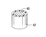
選択可能な他の実施例において、上述の方法は他の種類の電子装置の製造に用いられてもよい。例えば、高エネルギーディスクバリスタはその側部にガラス又はポリマーの絶縁層を有する。図3において、ディスクバリスタ40は、ガラス又はポリマーの代りに、上述の方法で形成されたリン酸塩の絶縁層42を有してもよい。本発明は図4に示される表装装置、放射状部品、配列、接続ピン、円盤状構造物等のような他のバリスタ製品に適用可能である。
【0014】
本発明は、無機電気絶縁層、露出した半導体表面を有する装置及び導電性金属の端部を備えた半導体装置を提供する。この装置はリン酸と反応し、金属端部上でなく、半導体の露出した表面上にリン酸塩を形成する。その後バレルが従来の電気バレルめっき法でめっきされ、めっきが端部上にのみ提供される。
尚、本発明は上述の実施例に限定されるものではなく、その主旨を逸脱しない範囲において適宜変更を加えることが可能である。
【図面の簡単な説明】
【図1】従来技術で典型的なバリスタを示す図である。
【図2】本発明の装置の実施例の縦断面図である。
【図3】本発明の絶縁層を備えた高エネルギーディスクバリスタの図である。
【図4】本発明の絶縁層を備えた表装型装置の図である。
【符号の説明】
20 非線形抵抗素子
24 酸化亜鉛半導体層
28 連結部
30 端部
32 端部領域
34 リン酸亜鉛層
40 ディスクバリスタ
42 絶縁層[0001]
BACKGROUND OF THE INVENTION
The present invention relates to a non-linear resistance device such as a varistor, and more particularly to a method for manufacturing such a device using barrel plating technology in which only the electrical contact end of the device is plated.
[0002]
[Prior art]
Nonlinear resistance devices are described in US Pat. No. 5,115,221.
FIG. 1 illustrates an
[0003]
The apparently simple structure of such devices contradicts their manufacturing complexity. For example, the attachment of
[0004]
It has been suggested that the metal forming the
[0005]
[Problems to be solved by the invention]
One object of the present invention is to provide a method and apparatus that eliminates the problems of the prior art, according to which an electrically insulating inorganic layer is formed on a part of the device before the device is barrel plated. Is done. Another object of the present invention is to react with the exposed surface of the zinc oxide semiconductor layer laminated with phosphoric acid to form a zinc phosphate coating, and when the edge is formed, the zinc phosphate coating is plated on the device. It is to provide a method and apparatus for protecting parts that are not present.
[0006]
Yet another object of the present invention is to provide a non-linear resistance device having a body of a layer of semiconductor material and an electrode between adjacent layers, the body of the non-linear resistance device having an electrode to an end terminal. Except for the end region of the body exposed for connection, it is covered with an electrically insulating inorganic layer, and the coated body is plated with a conductive metal to form an end terminal. In the plating method, the body becomes conductive and the inorganic layer is not conductive, so the conductive metal does not plate the coated portion of the body.
[0007]
[Means for Solving the Problems]
The present invention includes a method of manufacturing a non-linear resistance device, the method comprising:
(A) providing a body of a non-linear resistance device that is a zinc oxide semiconductor except for an end region where the end is provided with an end; and
(B) reacting phosphoric acid with the body to form an electrically insulating zinc phosphate coating on the exposed zinc oxide semiconductor without coating this end;
(C) It comprises a step of barrel plating the main body in order to plate the end portion with a conductive metal,
Since zinc phosphate is not conductive, conductive metal is not formed on the zinc phosphate coated portion of the body during barrel plating.
[0008]
The invention also includes a method of coating electrical connections for a varistor, the method comprising:
(A) providing an uncoated varistor having a plurality of zinc oxide layers intermediately provided with an electrode in contact with at least one of two external conductive metal ends separated by an exposed surface of the zinc oxide layer; When,
(B) An uncoated varistor is immersed in a phosphoric acid solution at 70 ° C. to 80 ° C. for 25 to 35 minutes to form an electrically insulating zinc phosphate coating except for the edges on the exposed surface of the zinc oxide layer. Stages,
(C) The coated varistor is processed by a barrel plating method. In this barrel plating method, the varistor is charged, the conductive plating substance adheres to the charged portion of the varistor, and the end is plated. The zinc phosphate coating is not plated.
[0009]
DETAILED DESCRIPTION OF THE INVENTION
Embodiments of the present invention will be described below with reference to the drawings.
FIG. 2 shows an embodiment of a non-linear
[0010]
[0011]
After the zinc phosphate layer is applied, the device is barrel plated with a conductive metal such as nickel and tin-lead to provide
[0012]
The
In other embodiments, the phosphate layer may be an inorganic oxide layer formed by reaction of phosphoric acid with a metal oxide semiconductor in the device. For example, the semiconductor may be iron oxide such as ferrite instead of zinc oxide.
[0013]
In other selectable embodiments, the method described above may be used in the manufacture of other types of electronic devices. For example, a high energy disc varistor has a glass or polymer insulating layer on its side. In FIG. 3, the
[0014]
The present invention provides a semiconductor device comprising an inorganic electrically insulating layer, a device having an exposed semiconductor surface, and an end of a conductive metal. This device reacts with phosphoric acid to form phosphate on the exposed surface of the semiconductor rather than on the metal edges. The barrel is then plated by a conventional electric barrel plating method, and plating is provided only on the edges.
In addition, this invention is not limited to the above-mentioned Example, In the range which does not deviate from the main point, it can add suitably.
[Brief description of the drawings]
FIG. 1 shows a typical varistor in the prior art.
FIG. 2 is a longitudinal sectional view of an embodiment of the apparatus of the present invention.
FIG. 3 is a diagram of a high energy disk varistor provided with an insulating layer of the present invention.
FIG. 4 is a view of a surface mount type apparatus provided with an insulating layer of the present invention.
[Explanation of symbols]
20
Claims (11)
(b)リン酸を本体と反応させて、露出している酸化亜鉛半導体上にこの端部は被覆されずに、電気的に絶縁性のリン酸亜鉛コーティングを形成する段階と、
(c)導電性金属で端部をめっきするため本体をバレルめっきする段階とよりなり、
リン酸亜鉛は導電性ではないので、導電性金属はバレルめっき中に本体のリン酸亜鉛コーティングされた部分上には形成されない非線形抵抗装置の製造方法。(A) providing a body of a non-linear resistance device that is a zinc oxide semiconductor except for an end region where the end is provided with an end; and
(B) reacting phosphoric acid with the body to form an electrically insulating zinc phosphate coating on the exposed zinc oxide semiconductor without coating this end;
(C) It comprises a step of barrel plating the main body in order to plate the end portion with a conductive metal,
A method of manufacturing a non-linear resistance device in which zinc phosphate is not conductive so that conductive metal is not formed on the zinc phosphate coated portion of the body during barrel plating.
(a)半導体装置をリン酸溶液にさらして、端部上でなく、露出した半導体表面上にリン酸塩コーティングを形成する段階と、
(b)半導体装置が帯電され、めっき溶液に浸漬されるという処理で導電性金属めっきで半導体装置をバレルめっきする段階とよりなり、リン酸塩コーティングは導電性でないので、めっきはリン酸塩コーティング上でなく、端部上に形成されることを特徴とする方法。6. The method of manufacturing a semiconductor device according to claim 1, further comprising: an inorganic electrical insulating layer; a semiconductor device having an exposed semiconductor surface; and a conductive metal edge. Exposing to an acid solution to form a phosphate coating on the exposed semiconductor surface rather than on the edges; and
(B) The semiconductor device is charged and immersed in a plating solution. The semiconductor device is then barrel-plated with conductive metal plating, and the phosphate coating is not conductive. A method , characterized in that it is formed on the end, not on.
(b)コーティングされていないバリスタを70℃から80℃で25から35分間リン酸溶液中に浸漬し、酸化亜鉛層の露出表面上に端部を除いて電気絶縁性リン酸亜鉛コーティングを形成する段階と、
(c)コーティングされたバリスタをバレルめっき法で処理する段階とよりなり、このバレルめっき法ではバリスタは帯電し、導電性めっき物質はバリスタの帯電部分に付着し、端部はめっきされるが、リン酸亜鉛コーティングはめっきされないバリスタの電気絶縁性コーティング方法。(A) providing an uncoated varistor having a plurality of zinc oxide layers intermediately provided with an electrode in contact with at least one of two external conductive metal ends separated by an exposed surface of the zinc oxide layer; When,
(B) An uncoated varistor is immersed in a phosphoric acid solution at 70 ° C. to 80 ° C. for 25 to 35 minutes to form an electrically insulating zinc phosphate coating except for the edges on the exposed surface of the zinc oxide layer. Stages,
(C) The coated varistor is processed by a barrel plating method. In this barrel plating method, the varistor is charged, the conductive plating substance adheres to the charged portion of the varistor, and the end is plated. Zinc phosphate coating is an electrically insulating coating method for varistors that are not plated.
前記層の各対間にあり各々は電気的接続のために露出した接触部を有するプレーナー電極と、
各々は前記接触部の少なくとも一に接触するための前記本体の端部である間隔をおいた複数の導電性金属端部と、
前記端部間の前記本体を被覆する電気的絶縁性のリン酸亜鉛コーティングと、 前記端部を被覆する金属めっきとよりなり、本体はモルパーセントで94−98%の酸化亜鉛と、酸化ビスマス、酸化コバルト、酸化マグネシウム、酸化ニッケル、酸化アンチモン、酸化ホウ素、酸化クロム、酸化ケイ素および硝酸アルミニウムからなる添加剤の群から選択された1又はそれ以上の2−6%の添加剤を含む非線形抵抗素子。A body constituted by a varistor having a laminated zinc oxide semiconductor layer;
A planar electrode between each pair of the layers, each having an exposed contact for electrical connection;
A plurality of spaced apart conductive metal ends, each being an end of the body for contacting at least one of the contact portions;
An electrically insulating zinc phosphate coating covering the body between the ends, and a metal plating covering the ends, the body comprising 94-98% zinc oxide in mole percent, bismuth oxide, Nonlinear resistive element comprising one or more 2-6% additives selected from the group of additives consisting of cobalt oxide, magnesium oxide, nickel oxide, antimony oxide, boron oxide, chromium oxide, silicon oxide and aluminum nitrate .
Applications Claiming Priority (2)
| Application Number | Priority Date | Filing Date | Title |
|---|---|---|---|
| US08/355,220 US5614074A (en) | 1994-12-09 | 1994-12-09 | Zinc phosphate coating for varistor and method |
| US355220 | 1994-12-09 |
Publications (2)
| Publication Number | Publication Date |
|---|---|
| JPH08227802A JPH08227802A (en) | 1996-09-03 |
| JP3634033B2 true JP3634033B2 (en) | 2005-03-30 |
Family
ID=23396675
Family Applications (1)
| Application Number | Title | Priority Date | Filing Date |
|---|---|---|---|
| JP31901195A Expired - Fee Related JP3634033B2 (en) | 1994-12-09 | 1995-12-07 | Non-linear resistance device manufacturing method, non-linear resistance device, and method for providing electrically insulating coating of varistor |
Country Status (4)
| Country | Link |
|---|---|
| US (2) | US5614074A (en) |
| EP (1) | EP0716429B1 (en) |
| JP (1) | JP3634033B2 (en) |
| DE (1) | DE69518612T2 (en) |
Families Citing this family (29)
| Publication number | Priority date | Publication date | Assignee | Title |
|---|---|---|---|---|
| KR100255906B1 (en) * | 1994-10-19 | 2000-05-01 | 모리시타 요이찌 | Electronic component and method for fabricating the same |
| JPH09205005A (en) * | 1996-01-24 | 1997-08-05 | Matsushita Electric Ind Co Ltd | Electronic component and manufacture thereof |
| ATE195198T1 (en) * | 1996-05-09 | 2000-08-15 | Littlefuse Inc | ZINC PHOSPHATE COATING FOR VARISTOR AND METHOD FOR PRODUCTION |
| DE19634498C2 (en) * | 1996-08-26 | 1999-01-28 | Siemens Matsushita Components | Electro-ceramic component and method for its production |
| TW394961B (en) * | 1997-03-20 | 2000-06-21 | Ceratech Corp | Low capacitance chip varistor and fabrication method thereof |
| GB2326976A (en) * | 1997-06-30 | 1999-01-06 | Harris Corp | Varistor nickel barrier electrode |
| JPH11191506A (en) * | 1997-12-25 | 1999-07-13 | Murata Mfg Co Ltd | Laminated varistor |
| US6214685B1 (en) * | 1998-07-02 | 2001-04-10 | Littelfuse, Inc. | Phosphate coating for varistor and method |
| US20020125982A1 (en) * | 1998-07-28 | 2002-09-12 | Robert Swensen | Surface mount electrical device with multiple ptc elements |
| JP2000091105A (en) * | 1998-09-11 | 2000-03-31 | Murata Mfg Co Ltd | Chip type ceramic thermistor and its manufacture |
| US6704997B1 (en) * | 1998-11-30 | 2004-03-16 | Murata Manufacturing Co., Ltd. | Method of producing organic thermistor devices |
| JP2001110666A (en) * | 1999-10-08 | 2001-04-20 | Murata Mfg Co Ltd | Electronic component, and manufacturing method thereof |
| US6535105B2 (en) * | 2000-03-30 | 2003-03-18 | Avx Corporation | Electronic device and process of making electronic device |
| US6841191B2 (en) * | 2002-02-08 | 2005-01-11 | Thinking Electronic Industrial Co., Ltd. | Varistor and fabricating method of zinc phosphate insulation for the same |
| KR100444888B1 (en) * | 2002-02-18 | 2004-08-21 | 주식회사 쎄라텍 | Chip type varistor and fabrication method thereof |
| JP4720825B2 (en) * | 2005-04-01 | 2011-07-13 | パナソニック株式会社 | Barista |
| EP1946336A1 (en) * | 2005-10-19 | 2008-07-23 | Littelfuse Ireland Development Company Limited | A varistor and production method |
| US20100189882A1 (en) * | 2006-09-19 | 2010-07-29 | Littelfuse Ireland Development Company Limited | Manufacture of varistors with a passivation layer |
| CN101350238B (en) * | 2007-07-16 | 2010-12-08 | 深圳振华富电子有限公司 | Method for processing surface of stacking slice type electronic element |
| JP2009200168A (en) * | 2008-02-20 | 2009-09-03 | Tdk Corp | Ceramic electronic component, ceramic electronic component manufacturing method and ceramic electronic component packing method |
| JP5211801B2 (en) * | 2008-03-28 | 2013-06-12 | Tdk株式会社 | Electronic components |
| US8195118B2 (en) * | 2008-07-15 | 2012-06-05 | Linear Signal, Inc. | Apparatus, system, and method for integrated phase shifting and amplitude control of phased array signals |
| US8872719B2 (en) * | 2009-11-09 | 2014-10-28 | Linear Signal, Inc. | Apparatus, system, and method for integrated modular phased array tile configuration |
| US20150010707A1 (en) * | 2013-07-02 | 2015-01-08 | Jian- Liang LIN | Method for Marking a Tool |
| JP6274044B2 (en) * | 2014-07-28 | 2018-02-07 | 株式会社村田製作所 | Ceramic electronic components |
| JP6339474B2 (en) * | 2014-10-03 | 2018-06-06 | アルプス電気株式会社 | Inductance element and electronic device |
| US11037710B2 (en) | 2018-07-18 | 2021-06-15 | Avx Corporation | Varistor passivation layer and method of making the same |
| CN112837877B (en) * | 2020-12-24 | 2022-06-17 | 南阳金铭电子科技有限公司 | Surface packaging treatment process for chip passive component |
| DE102022114552A1 (en) | 2022-06-09 | 2023-12-14 | Tdk Electronics Ag | Process for producing a multilayer varistor |
Family Cites Families (16)
| Publication number | Priority date | Publication date | Assignee | Title |
|---|---|---|---|---|
| US4046847A (en) * | 1975-12-22 | 1977-09-06 | General Electric Company | Process for improving the stability of sintered zinc oxide varistors |
| GB2004531A (en) * | 1977-09-09 | 1979-04-04 | Billington & Son Ltd E | Growing medium from paper strips |
| JPS5816602B2 (en) | 1979-02-09 | 1983-04-01 | ティーディーケイ株式会社 | Voltage nonlinear resistance element |
| DE3050770C2 (en) * | 1979-02-09 | 1987-03-19 | Tdk Corporation, Tokio/Tokyo, Jp | |
| US4371860A (en) * | 1979-06-18 | 1983-02-01 | General Electric Company | Solderable varistor |
| CA1186130A (en) * | 1981-06-16 | 1985-04-30 | Jeffery L. Barrall | Rigid, water-resistant phosphate ceramic materials and processes for preparing them |
| JPH0770380B2 (en) * | 1988-04-11 | 1995-07-31 | ローム株式会社 | Nickel plating method for electronic parts |
| US5075665A (en) * | 1988-09-08 | 1991-12-24 | Murata Manufacturing Co., Ltd. | Laminated varistor |
| JPH02189903A (en) * | 1989-01-18 | 1990-07-25 | Murata Mfg Co Ltd | Laminated varistor |
| JPH03131004A (en) * | 1989-10-17 | 1991-06-04 | Toshiba Corp | Manufacture of non-linear resistor |
| JPH03173402A (en) * | 1989-12-02 | 1991-07-26 | Murata Mfg Co Ltd | Chip varistor |
| GB2242066B (en) | 1990-03-16 | 1994-04-27 | Ecco Ltd | Varistor structures |
| JP2815990B2 (en) * | 1990-07-26 | 1998-10-27 | 株式会社東芝 | Manufacturing method of nonlinear resistor |
| US5307046A (en) * | 1991-05-22 | 1994-04-26 | Hubbell Incorporated | Passivating coating for metal oxide varistors |
| JPH05136012A (en) * | 1991-11-15 | 1993-06-01 | Rohm Co Ltd | Manufacture of chip-type electronic parts |
| ATE195198T1 (en) * | 1996-05-09 | 2000-08-15 | Littlefuse Inc | ZINC PHOSPHATE COATING FOR VARISTOR AND METHOD FOR PRODUCTION |
-
1994
- 1994-12-09 US US08/355,220 patent/US5614074A/en not_active Expired - Lifetime
-
1995
- 1995-12-07 JP JP31901195A patent/JP3634033B2/en not_active Expired - Fee Related
- 1995-12-08 DE DE69518612T patent/DE69518612T2/en not_active Expired - Lifetime
- 1995-12-08 EP EP95402769A patent/EP0716429B1/en not_active Expired - Lifetime
-
1997
- 1997-01-22 US US08/786,307 patent/US5757263A/en not_active Expired - Lifetime
Also Published As
| Publication number | Publication date |
|---|---|
| US5757263A (en) | 1998-05-26 |
| EP0716429B1 (en) | 2000-08-30 |
| DE69518612D1 (en) | 2000-10-05 |
| EP0716429A2 (en) | 1996-06-12 |
| US5614074A (en) | 1997-03-25 |
| DE69518612T2 (en) | 2001-05-03 |
| JPH08227802A (en) | 1996-09-03 |
| EP0716429A3 (en) | 1997-01-22 |
Similar Documents
| Publication | Publication Date | Title |
|---|---|---|
| JP3634033B2 (en) | Non-linear resistance device manufacturing method, non-linear resistance device, and method for providing electrically insulating coating of varistor | |
| US6214685B1 (en) | Phosphate coating for varistor and method | |
| US6159768A (en) | Array type multi-chip device and fabrication method therefor | |
| JP3497840B2 (en) | Manufacturing method of chip varistor having glass coating film | |
| US6232144B1 (en) | Nickel barrier end termination and method | |
| US6841191B2 (en) | Varistor and fabricating method of zinc phosphate insulation for the same | |
| RU2159482C2 (en) | Connecting leads of electronic component (design versions), electronic component (design versions) and its manufacturing process (options) | |
| US3310718A (en) | Impedance element with alloy connector | |
| US4342020A (en) | Electrical network | |
| EP0806780B1 (en) | Zinc phosphate coating for varistor and method | |
| EP0186765B1 (en) | End termination for chip capacitor | |
| US6278065B1 (en) | Apparatus and method for minimizing currents in electrical devices | |
| JP3092451B2 (en) | Rectangular thin film chip resistor and method of manufacturing the same | |
| EP0973176A1 (en) | Nickel barrier end termination and method | |
| US3429788A (en) | Electrical interconnection of micromodule circuit devices | |
| JPS634327B2 (en) | ||
| TWI760706B (en) | Electronic component packaging structure and manufacturing method thereof | |
| US5308686A (en) | Substrate having a multiple metal protected conductive layer and method of manufacturing the same | |
| JPH08330105A (en) | Electronic component | |
| JPS6228746Y2 (en) | ||
| JPS6311792B2 (en) | ||
| JPH0397212A (en) | Chip type solid-state electrolytic capacitor | |
| US20080012127A1 (en) | Insulation structure for multilayer passive elements and fabrication method thereof | |
| JPH043444Y2 (en) | ||
| JPH0458188B2 (en) |
Legal Events
| Date | Code | Title | Description |
|---|---|---|---|
| A977 | Report on retrieval |
Free format text: JAPANESE INTERMEDIATE CODE: A971007 Effective date: 20040420 |
|
| A131 | Notification of reasons for refusal |
Free format text: JAPANESE INTERMEDIATE CODE: A131 Effective date: 20040427 |
|
| A601 | Written request for extension of time |
Free format text: JAPANESE INTERMEDIATE CODE: A601 Effective date: 20040726 |
|
| A602 | Written permission of extension of time |
Free format text: JAPANESE INTERMEDIATE CODE: A602 Effective date: 20040729 |
|
| A521 | Request for written amendment filed |
Free format text: JAPANESE INTERMEDIATE CODE: A523 Effective date: 20041026 |
|
| TRDD | Decision of grant or rejection written | ||
| A01 | Written decision to grant a patent or to grant a registration (utility model) |
Free format text: JAPANESE INTERMEDIATE CODE: A01 Effective date: 20041130 |
|
| A61 | First payment of annual fees (during grant procedure) |
Free format text: JAPANESE INTERMEDIATE CODE: A61 Effective date: 20041222 |
|
| R150 | Certificate of patent or registration of utility model |
Free format text: JAPANESE INTERMEDIATE CODE: R150 |
|
| FPAY | Renewal fee payment (event date is renewal date of database) |
Free format text: PAYMENT UNTIL: 20090107 Year of fee payment: 4 |
|
| FPAY | Renewal fee payment (event date is renewal date of database) |
Free format text: PAYMENT UNTIL: 20090107 Year of fee payment: 4 |
|
| FPAY | Renewal fee payment (event date is renewal date of database) |
Free format text: PAYMENT UNTIL: 20090107 Year of fee payment: 4 |
|
| FPAY | Renewal fee payment (event date is renewal date of database) |
Free format text: PAYMENT UNTIL: 20090107 Year of fee payment: 4 |
|
| FPAY | Renewal fee payment (event date is renewal date of database) |
Free format text: PAYMENT UNTIL: 20100107 Year of fee payment: 5 |
|
| FPAY | Renewal fee payment (event date is renewal date of database) |
Free format text: PAYMENT UNTIL: 20110107 Year of fee payment: 6 |
|
| LAPS | Cancellation because of no payment of annual fees |