JP3629552B2 - Computer backplane hot plug circuit manufacturing test - Google Patents
Computer backplane hot plug circuit manufacturing test Download PDFInfo
- Publication number
- JP3629552B2 JP3629552B2 JP2001052041A JP2001052041A JP3629552B2 JP 3629552 B2 JP3629552 B2 JP 3629552B2 JP 2001052041 A JP2001052041 A JP 2001052041A JP 2001052041 A JP2001052041 A JP 2001052041A JP 3629552 B2 JP3629552 B2 JP 3629552B2
- Authority
- JP
- Japan
- Prior art keywords
- backplane
- hot plug
- test
- slot
- adapter
- Prior art date
- Legal status (The legal status is an assumption and is not a legal conclusion. Google has not performed a legal analysis and makes no representation as to the accuracy of the status listed.)
- Expired - Fee Related
Links
Images


Classifications
-
- G—PHYSICS
- G06—COMPUTING OR CALCULATING; COUNTING
- G06F—ELECTRIC DIGITAL DATA PROCESSING
- G06F13/00—Interconnection of, or transfer of information or other signals between, memories, input/output devices or central processing units
- G06F13/38—Information transfer, e.g. on bus
- G06F13/40—Bus structure
- G06F13/4063—Device-to-bus coupling
- G06F13/409—Mechanical coupling
-
- G—PHYSICS
- G06—COMPUTING OR CALCULATING; COUNTING
- G06F—ELECTRIC DIGITAL DATA PROCESSING
- G06F13/00—Interconnection of, or transfer of information or other signals between, memories, input/output devices or central processing units
Landscapes
- Engineering & Computer Science (AREA)
- Theoretical Computer Science (AREA)
- General Engineering & Computer Science (AREA)
- Physics & Mathematics (AREA)
- General Physics & Mathematics (AREA)
- Computer Hardware Design (AREA)
- Test And Diagnosis Of Digital Computers (AREA)
Description
【0001】
【発明の属する技術分野】
本発明は、一般にコンピュータ・バックプレーンの回路のテストに関し、特にアクティブなコンピュータ・バックプレーンの各スロットに対応したホット・プラグ回路をテストする方法及び装置に関する。
【0002】
【従来の技術】
プロセッサ、キャッシュ、メモリ、拡張カード及びストレージ・デバイス等、コンピュータの内部コンポーネントはバスを介して相互に通信する。バスは、コンピュータの用語では、デバイス間で情報が流れるチャネルである。通常、バスには、デバイスがバスの一部になるためにインタフェースを取る場所であるアクセス・ポイントがある。デバイスは、バスとインタフェースを取ると、同じくバスとインタフェースを取っている他のデバイスとの間で情報を送受信することができる。
【0003】
現在生産されているほぼ全てのPCに、ビデオ・データ等、高速転送を必要とするデータのローカル・バスがある。ローカル・バスは、周辺装置(ビデオ・カード、サウンド・カード、モデム等)をプロセッサに直接接続する高速経路である。現在、最も一般的なローカル・バスは、インテル社が開発し1993年に発表したPCI(Peripheral Component Interconnect)バスである。
【0004】
近年のPCIバスの発展の中で最も重要なのはホット・プラグ技術である。ホット・プラグは、一般にはコンピュータが動作中にコンピュータとの間でデバイスの追加や削除を行い、オペレーティング・システムがその変更を自動的に認識する機能として定義される。PCIのSIG(Special Interest Group)により、システム・プロバイダ、オペレーティング・システム・デベロッパ、及びアダプタ・サプライヤがPCIホット・プラグ・ソリューションを実装することのできるオープンな業界標準が開発されている。PCIホット・プラグ技術では、旧式のバス・アーキテクチャとは異なり、ホスト・システムが動作中、またコンピュータ・システムの他のアダプタによるサービスを中断することなく、PCIアダプタを追加、削除、または交換できる。その結果PCIホット・プラグ技術は、予定外のシステム・ダウンタイムを大幅に短縮することができる。それまでは、常時信頼できるパフォーマンスを得られるのは、高価で独占的なシステムに限られていた。
【0005】
ホット・プラグ回路を支えるPCIバックプレーンのメーカにとっては、PCIホット・プラグ回路自体の機能テスト(つまりホット・プラグ回路により、関連するアダプタ・スロットの電源投入/遮断を適切に行えるかどうか)が大きな課題である。バックプレーンのメーカの標準ICT(インサーキット・テスト)によりホット・プラグ回路を十分にテストすることはできない。ホット・プラグ回路の検出レジスタは抵抗が小さすぎ、短絡と区別できないためである。その結果ホット・プラグ回路のテストは、テスト対象のホット・プラグ回路に対応するPCIスロットに取り付けて2つの別個のテスト・アダプタ・カード(つまりアナログ・テスト用アナログ・カードとデジタル・テスト用デジタル・カード)により実施する必要がある。これにより、バックプレーンをテスト・ステーションに置いておく時間は倍になり、バックプレーン・テスト機構はかなり複雑になり、コストも大幅に増える。
【0006】
従って、コンピュータ・システムのアクティブなPCIバックプレーン上のPCIホット・プラグ回路を時間をかけずにテストする費用効率が高い方法及び装置が求められる。この方法及び装置では、スロットのPCIデジタル・テストを行う場合と同じメーカのテスト・アダプタによりアナログ・テストを行うことにより、バックプレーンをテストするため取付具に固定しておく時間を短縮することが求められる。またこの方法と装置により、PCIバックプレーン上のPCIホット・プラグ回路の開発テストを改良し、外部テスト・コネクタを介して詳細な測定値をPCIバックプレーンから直接得ることが求められる。
【0007】
【発明が解決しようとする課題】
本発明は、コンピュータ・バックプレーン上のホット・プラグ回路をテストする方法及び装置を提供する。
【0008】
【課題を解決するための手段】
好適実施例では、各バックプレーンのテスト・コネクタにより外部テスタとの間の信号がバックプレーンに送られ、特にコンピュータ・バックプレーンに装着されたカード・スロットそれぞれに供給される電力を制御するホット・プラグ回路に送られる。
【0009】
外部テスタは、テスト・コネクタにより、コンピュータ・バックプレーンにある各カード・スロットの電源を入れることができる。次に外部テスタは、選択されたカード・スロットにあるテスト・アダプタ・カードに、選択されたカード・スロットの各電圧レベルに公称負荷または過電流負荷を印加するよう指示する。負荷がそれぞれ印加された後、対応する電圧レベルが外部テスタに返される。外部テスタは次に電圧レベルを測定し、既定電圧範囲にあることを確認する。テスト・コネクタには、テスト対象のカード・スロットと外部テスタとの間でテストの指示内容と結果をやりとりするため、既存の未使用バス信号ラインが用いられる。カード・スロットでアナログ・テストを行う場合と同じテスト・アダプタ・カードが、カードのデジタル・テストにも用いられ、テスト時間が短縮され、テスト装置を複雑にする必要がなくなる。
【0010】
本発明は、ホット・プラグ回路の現在のテスト方法にはないメリットを与える。好適実施例では、デジタル・テストの場合と同じテスト・アダプタによりホット・プラグ回路のアナログ・テストが行え、予想されるテスト時間が半分になる。1つのテスト・アダプタ・カードをアナログとデジタルの両方のテストに使用できるので、回路テストに必要な取付具の複雑さは減少する。また好適実施例では、テスト・コネクタを介して詳細な測定値を容易に、時間をかけずに得ることができるので、ホット・プラグ回路の開発テストが改良される。
【0011】
【発明の実施の形態】
図1は、ホット・プラグ回路を組み込んだコンピュータ・システム20の基本コンポーネントを示す機能ブロック図である。前記のように、ホット・プラグ回路によりコンピュータが動作中、またオペレーティング・システムにより変更を自動的に認識しながら、コンピュータとの間でデバイスの追加や削除ができる。好適な実施例の場合、コンピュータ・システム20は、PCIのSIG(Special Interest Group)により開発されたPCIホット・プラグ仕様1.0に従ったPCI(Peripheral Component Interconnect)バスを使用する。ただし、ホット・プラグ回路の一般的概念を採用した他のタイプのバックプレーンも、本発明の範囲内でサポートされる。
【0012】
当該実施例で、コンピュータ・システム20は少なくとも1つのソフトウェア層22と少なくとも1つのハードウェア層24を含む。ソフトウェア層22にはオペレーティング・システム26が含まれ、オペレーティング・システム26はホット・プラグ・サービス28を含む。ホット・プラグ・サービス28は、ホット・プラグ動作全体を制御するソフトウェアである。オペレーティング・システム26はまたホット・プラグ・システム・ドライバ32を含む。ドライバ32はホット・プラグ・コントローラ38(後述)を制御/監視する。ホット・プラグ・サービス28はリクエスト(ホット・プラグ・プリミティブ36ともいう)をホット・プラグ・システム・ドライバ32に発行し、アダプタ・カード・スロットのオン/オフを行う。ホット・プラグ・サービス28はまた、オペレーティング・システムにリクエストを発行し、アダプタのアクティビティを休止させることができる(つまりアダプタ・アクティビティが休止したとき、アダプタ・ドライバ40はアダプタ・カード50にオペレーションを送らず、アダプタ・カード50は割込みやバス・マスタ・アクティビティを開始しない)。
【0013】
ホット・プラグ・サービス28は、ホット・プラグ・サービスにアクセスするとき、(APIを介して)ユーザ30と管理エージェント31のゲートウェイになる。ホット・プラグ・サービス28は、各オペレーティング・システムに固有であり、一般にはオペレーティング・システムのベンダが供給する。ソフトウェア層22にはアダプタ・ドライバ40も含まれる。アダプタ・ドライバ40は、アダプタ・カード50を制御するソフトウェアである。アダプタ・ドライバ40は一般にアダプタ・カードのベンダにより供給される。
【0014】
ハードウェア層24は、バス48が存在するハードウェアの集合であるプラットフォーム44を含む。プラットフォーム44は通常、電源、CPU、ブリッジ(ホスト・バスとPCIのブリッジ等)、その他ディスク・ドライブ、キーボード等の各種周辺装置を含む。プラットフォーム44はまたホット・プラグ・コントローラ38を含む。コントローラ38は、プラットフォーム・ベンダが供給するハードウェアで、スロット46の電源の投入や遮断の電気的側面を制御する。
【0015】
スロット46は、アダプタ・カード50を受け取るよう設計されたバス48上の場所である。スロット46はホット・プラグ機能の基本ユニットである。アダプタ・カード50の取り付けと取り外しに信頼性を持たせるには、プラットフォーム44の残りの部分から個々のスロット46を分離する必要がある。アダプタ・カード50は、実施例では、PCIローカル・バス仕様に従って設計されたカードであり、スロット46に取り付けられるよう設計される。他の実施例では、32ビット幅或いは64ビット幅で、33MHz或いは66MHzで動作し、3.3V或いは5Vのシグナリングを行う。アダプタ・カード50は、単一デバイスを格納またはブリッジを介して複数のデバイスを格納することができる。
【0016】
単一のホット・プラグ・コントローラ38は通常、スロット46を2つ以上制御するが、ホット・プラグ・コントローラ38とスロット46の1対1対応は、実施例の範囲内で可能である。プラットフォーム44は通常、ホット・プラグ・コントローラ38を2つ以上含むが、単一のホット・プラグ・コントローラを使用することも本発明の範囲内である。アテンション・インディケータ51は、ユーザが特定のスロット46に注意を向けるようにする物理インディケータである。実施例のアテンション・インディケータ51はLED(発光ダイオード)等である。
【0017】
通常動作時、電源の入っているスロット46からアダプタ・カード50を取り外すまたは交換する必要があるとき、通常は次のステップが実行される。まずユーザ30が、アダプタ・カード50をスロット46から取り外したい旨をホット・プラグ・サービス28に通知する。通知方法としては、コンソール・コマンドの発行、そのためのスイッチのアクティブ化等がある。次にホット・プラグ・サービス28によりオペレーティング・システムの機能が使用され、対応するアダプタ・ドライバ40及びアダプタ・カード50が休止される。ホット・プラグ・サービス28は次にホット・プラグ・プリミティブ36をホット・プラグ・システム・ドライバ32に発行し、対応するスロット46をオフにする。ホット・プラグ・システム・ドライバ32は、これに応答してホット・プラグ・コントローラ38を使用し、1)スロット46へのリセット・ラインをアサートし、バス48の残りの部分からスロット46を分離し、2)スロット46の電源を遮断し、3)アテンション・インディケータ51を変更してスロット46がオフであることを示す。ホット・プラグ・サービス28は次に、スロット46がオフであることをユーザ30に報告する。最後にユーザ30はアダプタ・カード50をスロット46から取り外す。
【0018】
同様に、スロットの電源が遮断されてカードを挿入する準備ができた後、スロット46にアダプタ・カード50を挿入するには、次の一般的なシーケンスが必要である。まずユーザ30は新しいアダプタ・カード50を対応するスロット46に挿入する。次にユーザ30は、新しいアダプタ・カード50が入ったスロットをオンにすることをホット・プラグ・サービス28に通知する。ホット・プラグ・サービスはホット・プラグ・システム・ドライバ32にホット・プラグ・プリミティブを発行し、対応するスロット46をオンにする。ホット・プラグ・システム・ドライバ32はホット・プラグ・コントローラ38に、1)スロット46の電源を入れ、2)スロット46へのリセット・ラインをアサート解除してスロット46をバスの残りの部分に接続し、3)アテンション・インディケータ51を変更してスロット46がオンであることを示すよう指示する。ホット・プラグ・サービス28は次に、新しいアダプタ・カード50が取り付けられたことをオペレーティング・システム26に通知する。これによりオペレーティング・システム26は新しいアダプタ・カード50を初期化し、使用できるよう準備する。最後にホット・プラグ・サービス28は、新しいアダプタ・カード50が使用できる状態にあることをユーザ30に通知する。
【0019】
好適実施例は、プラットフォーム44内にテスト・コネクタ102を組み込んでいる。外部テスタ103は、テスト中、コネクタ102により、ホット・プラグ・コントローラ38を有効/無効にすることができ、よって外部テスタ103はバックプレーンの各スロット46に直接アクセスできる。テスト・コネクタ102は、バス内の既存の未使用信号を使用してテストの指示内容や結果を外部テスタ103とテスト対象スロット46の間でやりとりする。テスト・コネクタ102については図2に関して詳述する。
【0020】
図2は、概略を要素100として示した、好適実施例に従ったホット・プラグ・バックプレーンのブロック図である。好適実施例のバックプレーン100はPCIバックプレーンであるが、好適実施例と同様のホット・プラグ動作をサポートするバックプレーンは本発明の範囲内であると考えられる。
【0021】
バックプレーン100はプラットフォーム(図1、要素44)内に位置し、一般には他の回路ボードが取り付けられるソケットを含む回路ボードとして定義される。バックプレーン100はアクティブまたはパッシブとして説明されることが多い。アクティブ・バックプレーンは、ソケットの他に半導体コンポーネントを含む。パッシブ・バックプレーンは、アクティブ・バックプレーンとは対照的に、論理モジュールを含まない。
【0022】
好適実施例ではアクティブ・バックプレーン100が採用される。バックプレーン100は、バス48、複数のスロット46、複数のスロット46それぞれに関連付けられたホット・プラグ回路101、アダプタ・カード(図1の要素50)、少なくとも1つのホット・プラグ・コントローラ38、及びバックプレーン・テスト・コネクタ102(後述)を含む。
【0023】
好適実施例で、テスト・コネクタ102はバックプレーン100表面に直接装着される。信号はテスト・コネクタ102から、バス48上の信号ラインを介してホット・プラグ・コントローラ・チップ38、ホット・プラグ回路101、及びスロット46に送られる。テスト・コネクタ102は、他の実施例では塞がれないが、テスト用取付具により下げられ、塞がれていないコネクタ102のピンに直接接触するようテスタ・コネクタにより用いられる。
【0024】
好適実施例の場合、テスト・コネクタ102はGROUND信号104、#RESET信号106、及びバックプレーン100上の各スロット46の3つの個別信号(#SLOT_ON108、TDO110、TCK112)を含む。GROUND信号104はバックプレーンのグランド電位である。#RESET信号106は各ホット・プラグ・コントローラ・チップ38を接続する。#RESET信号106がアサートされたとき、ホット・プラグ・コントローラ・チップ38はリセット状態に保たれ、ホット・プラグ回路101の制御が解除される。#SLOT_ON信号108は各ホット・プラグ回路101にワイヤ接続され、#RESET信号106がアサートされたときに、テスト・コネクタ102を通して#SLOT_ON信号108をアサート/アサート解除することによって特定のホット・プラグ回路101をオン/オフ切り替えることができる。ホット・プラグ回路101は、(過電流等で)遮断されたときは、#SLOT_ON信号108を切り替えてホット・プラグ回路をオンに戻す必要がある。
【0025】
好適実施例で、TDO信号110とTCK信号112は、PCIスロット・コネクタ46のPCI仕様信号である。JTAGを使用しないPCIバックプレーンのPCI仕様に述べられている通り、TDO信号110はどこにも接続されず、TCK信号112にはプルダウン抵抗が用いられる。これらの信号は通常バックプレーン100では使用されないので、好適実施例では、各スロット46をテスト・コネクタ102に接続するためにこれらの未使用信号が用いられる。
【0026】
TCK信号112は、テスト・コネクタ102からテスト・アダプタ・カード53上の制御ロジックへのシリアル通信ラインとして用いられる。アダプタ・カード53については図3とあわせて詳述する。TCK信号112は、スロット46に供給される4つの切り替え電圧(+3.3V、+5V、+12V、−12V)それぞれに対してテスト・アダプタ・カード53により印加される負荷抵抗(公称負荷または過電流負荷)を制御するため用いられる。
【0027】
TDO信号110は、選択されたホット・プラグ切り替え電圧に負荷抵抗が印加された後に、切り替え電圧の出力を返すために用いられる。テスト・コネクタ102に接続された外部テスタ103は、TDO信号110を監視することによって、テスト・アダプタ・カード53により印加され選択された調整済み負荷抵抗により切り替え電圧が遮断されているかどうかを観察する。
【0028】
バックプレーンのメーカは、比較的安価なバックプレーン・テスト・コネクタ102を標準アクティブ・ホット・プラグ・バックプレーン100に追加することにより、各スロット46を外部からオンにし、負荷の変動により各スロット電圧を過電流にし、過電流レベルを測定し、過電流が正規範囲内にあることを確認することができる。バックプレーンがこの機能テストに合格しない場合、バックプレーン・メーカは、バックプレーン100上のスロット46のホット・プラグ回路101に製造組み立ての問題(つまり故障)があることを知る。
【0029】
図3は、テスト・アダプタ・カード53の好適実施例のブロック図である。テスト・アダプタ・カード53は、先に図2に示したアクティブ・ホット・プラグ・バックプレーン100のスロット(図1、要素46)に挿入される。テスト・アダプタ・カード53は、テスト・コネクタ102からTCK信号112(つまりシリアル通信ライン)を介してコマンドを受け取り、応答信号153を生成する負荷抵抗コントローラ152を含む。応答信号153は、切り替え電圧156に印加するのに適した負荷抵抗154を選択する。負荷抵抗コントローラ152からマルチプレクサ160にはマルチプレクサ選択信号158が送られ、切り替え電圧156が選択され、TDO信号110を介して外部テスタ103に返される。
【0030】
ホット・プラグ回路101のアナログ負荷抵抗テストの場合と同じテスト・アダプタ・カード53が、デジタル・テストにも用いられる。アナログ・テスト時に用いられたのと同じ信号がデジタル・テスト時にも用いられることはないためである。デジタル・テストを行うため、PCIアダプタ・カード50がPCIアダプタ・コネクタ155を介してテスト・アダプタ・カード53に取り付けられる。
【0031】
図4及び図5は、好適実施例に従ってアクティブ・コンピュータ・バックプレーン100上のホット・プラグ回路101をテストする方法を示すフローチャートである。アクティブ・コンピュータ・バックプレーン100は、好適実施例ではPCIバックプレーンであるが、図4及び図5の方法は、ホット・プラグ対応PCIバックプレーン内に採用されるものと同様のホット・プラグ技術を採用した任意のバックプレーンに適用することができる。
【0032】
方法はまず、ブロック161に示すように、テスト・アダプタ・カード53をテスト対象のスロット46に挿入することから始まる。先に述べた通り、テスト・アダプタ・カード53は、外部テスタ103から負荷抵抗コマンドを受け取り、選択された負荷抵抗を、テスト対象スロットに選択された電圧レベルに印加する負荷抵抗コントローラ152を含む。
【0033】
次にブロック162で、外部テスタ103がバックプレーン・テスト・コネクタ102に接続される。外部テスタ103は、負荷抵抗コマンドをTCK信号112を介してテスト・アダプタ・カード53に転送し、選択された負荷抵抗154が選択された切り替え電圧156に印加された後、テスト・アダプタ・カード53から切り替え電圧を受信/測定できる任意のデバイスである。
【0034】
ブロック164で、外部テスタ103がバックプレーン・テスト・コネクタ102に接続された後、バックプレーン100上のホット・プラグ・コントローラ・チップ38がリセット状態に保たれ、バックプレーン100上のホット・プラグ回路101の制御を解除するよう、外部テスタ103によって#RESET信号106がアサートされる。#RESET信号106をアサートすることによって、各スロット46(及びこれに関連するホット・プラグ回路101)の電源投入/遮断とアドレス指定を外部テスタ103によって個別に行える。
【0035】
ブロック166で、外部テスタ103が、#SLOT_ON信号108をアサートすることによって、テスト・アダプタ・カード53を含むスロット46をアクティブにする。テスト・アダプタ・カード53を含むスロット46がオンになった後、外部テスタ103からテスト・アダプタ・カード53にコマンドが発行され、スロット46の切り替え電圧に公称負荷電圧が印加される(ブロック168)。切り替え電圧に印加される公称負荷電圧は、関連するホット・プラグ回路101が正常に動作している場合には公称負荷電圧の印加によってホット・プラグ回路101がスロット46を遮断することのないように選択される。
【0036】
電圧レベル+3.3Vの通常の過電流限度は、好適実施例では、約11アンペア乃至約14.5アンペアなので、公称負荷電圧は、電流が11アンペア未満になるよう選択される。電圧レベル+5Vの通常の過電流限度は、約8.2アンペア乃至約11.2アンペアなので、公称負荷電圧は電流が8.2アンペア未満になるよう選択される。同様に、電圧レベル+12Vの通常の過電流限度は、約0.86アンペア乃至約1.24アンペアなので、公称負荷電圧は電流が0.86アンペア未満になるよう選択される。また電圧レベル−12Vの通常の過電流限度は、約0.2アンペア乃至約0.34アンペアなので、公称負荷電圧は電流が0.2アンペア未満になるよう選択される。電圧レベルと電圧レベルに対応した動作限度は、他の実施例では変化し得る。
【0037】
テスト・アダプタ・カード53によってカードの切り替え電圧に公称負荷電圧が印加された後(ブロック168)、切り替え電圧レベルが外部テスタ103により測定される(ブロック170)。ブロック172で、公称負荷電圧の印加によりアダプタ・カード・スロット46が遮断されたことが外部テスタ103により確認された場合、外部テスタ103はエラーを記録し、テストは終了する(ブロック173)。故障したバックプレーンは修復に送られる。テスト・アダプタ・カード53による公称負荷電圧の印加によって、アダプタ・カード・スロットが遮断されない場合(正常状態)、処理はブロック174に進む。
【0038】
ブロック174で外部テスタ103からテスト・アダプタ・カード53にコマンドが発行され、カード46の選択された切り替え電圧に切り替え過電流負荷が印加される。選択された切り替え電圧に印加される過電流負荷は、ホット・プラグ回路101が正常に動作している場合に、過電流負荷の印加により、関連するホット・プラグ回路101がスロット46を遮断しないように選択される。実施例で、電圧レベル+3.3Vの動作限度は約11アンペア乃至約14.5アンペアなので、過電流負荷は電流が14.5アンペアを超えるよう選択される。電圧レベル+5Vの動作限度は約8.2アンペア乃至約11.2アンペアなので、過電流負荷は電流が11.2アンペアを超えるよう選択される。同様に、電圧レベル+12Vの動作限度は約0.86アンペア乃至約1.24アンペアなので、過電流負荷は電流が1.24アンペアを超えるよう選択される。また電圧レベル−12Vの動作限度は約0.2アンペア乃至約0.34アンペアなので、過電流負荷は電流が0.34アンペアを超えるよう選択される。
【0039】
テスト・アダプタ・カード53によりカードの切り替え電圧に過電流負荷が印加された後(ブロック174)、切り替え電圧レベルが測定される(ブロック176)。ブロック178で、過電流負荷印加によりアダプタ・カード・スロット46が遮断されたかどうかが確認される。アダプタ・カード・スロットが遮断されない場合、外部テスタ103はエラーを記録する(ブロック179)。過電流負荷の印加によりスロット46が遮断された場合(正常状態)、外部テスタ103によりコマンドが発行され、カード・スロット46の電源が再投入されて次の負荷抵抗テストが行われる(ブロック180)。
【0040】
テスト・アダプタ・カード53によりカード・スロット46の選択された電圧レベルに公称負荷と過電流負荷が印加された後、テスト対象のカード・スロット46について電圧レベルを追加してテストする必要があるかどうかが確認される(ブロック182)。必要がある場合、テスト対象スロット46の残りの全ての電圧レベルについて負荷抵抗テスト(ブロック168乃至178)が繰り返され(ブロック183)、必要ない場合、処理はブロック184に進む。
【0041】
テスト・アダプタ・カード53により公称負荷電圧と過電流負荷電圧がテスト対象のカード・スロット46の全ての電圧レベルに印加された後、バックプレーン100で他のカード・スロット46をテストする必要があるかどうかが確認される(ブロック184)。必要がある場合、テスト・アダプタ・カード53が、バックプレーン上の空いている次のスロット46に挿入され(ブロック186)、新しく選択されたカード・スロット46について抵抗テストと測定(ブロック166乃至182)が繰り返される。実施例では、バックプレーン・テスト時に必要なオペレータの手間を最小限にするため、複数のアダプタが用いられる。
【0042】
最後に、バックプレーン100上の全てのカード・スロット46の全ての電圧レベルについて、テスト・アダプタ・カード53により公称負荷電圧と過電流負荷電圧が印加された後、バックプレーンの複数のスロット46に対してテスト・アダプタ・カード53によってデジタル・テストが行われる(ブロック188)。デジタル・テスト中、テスト・アダプタ・カード53にPCIアダプタ50が取り付けられる。他の実施例では、所定のスロットでアナログ・テストが完了した直後に、所定のスロットに対してデジタル・テストが行われる。
【0043】
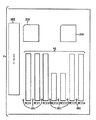
図6及び図7は、ホット・プラグ・バックプレーン100の好適実施例を示す。好適実施例で、ホット・プラグ・バックプレーン100はPCIバックプレーンであるが、他のタイプのホット・プラグ型バックプレーンも本発明の範囲内である。図の例でバックプレーン100はバス(図1、要素48)に中央コネクタ202を介して接続される。好適実施例の場合、バックプレーン100は合計14のカード・スロット46を含む(うち10のカード・スロットは64ビット、3.3Vのスロット、うち4つは32ビット、5Vのスロット)。他の実施例では、ホット・プラグ・バックプレーン上のカードの数とタイプは変わり得る。
【0044】
図のバックプレーン100はまた、14のカード・スロット46を管理する3つのホット・プラグ・コントローラ204、206、208を含む。第1ホット・プラグ・コントローラ204はカード・スロット1乃至4を、第2ホット・プラグ・コントローラ206はカード・スロット5乃至9を、第3ホット・プラグ・コントローラ208はカード・スロット10乃至14をそれぞれ管理する。他の実施例では、バックプレーン100に採用されるホット・プラグ・コントローラの数と構成は変わり得る。
【0045】
14のカード・スロット46それぞれに、カード・スロット46の電圧レベルを制御するホット・プラグ回路101が関連付けられる。バックプレーン100はまた、ホット・プラグ回路101のアナログ・テストに用いられる外部テスタ103に接続されるテスト・コネクタ102を含む。
【0046】
図8乃至図12は、好適実施例に従ってバックプレーン100の電圧に負荷抵抗を印加するテスト・アダプタ・カード53上のマイクロプロセッサ220を示す。図の例で、外部テスタ103からマイクロプロセッサ220に、テスト・コネクタ102を介してTCK信号112が送られる。前記のように、TCK信号112は、テスト・コネクタ102からのシリアル通信ラインとして、テスト・アダプタ・カード53のロジックを制御するため用いられる。TCK信号112は、4つの切り替え電圧(+3.3V、+5V、+12V、−12V)それぞれについて、テスト・アダプタ・カード53の負荷抵抗(公称負荷と過電流負荷)を制御するため用いられる。マイクロプロセッサ220は、TCK信号112を外部テスタ102から受け取った後、3ビット・マルチプレクサ・アドレス・バス222及び関連するラッチ・データ信号224とラッチ・イネーブル信号226を介して選択負荷をラッチに送る。3ビット・マルチプレクサ・アドレス・バス222は、選択可能な8つの負荷抵抗(公称+3.3V、過負荷+3.3V、公称+5V、過負荷+5V、公称+12V、過負荷+12V、公称−12V、過負荷−12V)を表すことができる。マイクロプロセッサ220はまた、選択信号+K1_RESET228、+K1_SET230、+K2_RESET232、+K2_SET234を出力電圧選択マルチプレクサ236(図13乃至図15に関して後述)に出力し、外部テスタに返すのに適した電圧信号を選択する。
【0047】
図13乃至図15は、テスト・アダプタ・カード53上の電圧選択マルチプレクサ236を示す図である。マルチプレクサ236は、好適実施例に従って、テスト・コネクタ102を介して外部テスタ103に選択された電圧(TDO110)を返す。マルチプレクサ236は2つのリレー250、252を含む。リレーのこの組み合わせは4:1マルチプレクサを形成する。4つの電圧(+3.3V、+5.0V、+12V、−12V)が第1リレー250に入力される。マイクロプロセッサ220により生成された選択信号+K1_RESET228と+K1_SET230が、第1リレー250の選択信号として与えられる。第1リレー250から4つの電圧のうち2つが選択され、第2リレー252への入力として与えられる。マイクロプロセッサ220により生成された選択信号+K2_RESET232と+K2_SET234が第2リレー252への入力として与えられる。第2リレー252から2つの電圧のうちいずれかが選択され、TDO信号110を介して外部テスタ103に返される。先に述べた通り、TDO信号110は外部テスタ103に切り替え電圧信号を与える。この信号は、選択された切り替え電圧信号にテスト・アダプタ・カード63によって印加された負荷抵抗により、現在テスト中のスロット46が遮断されているかどうかを示す。
【0048】
図16乃至図19は、好適実施例に従ったホット・プラグ回路101を示す。ホット・プラグ回路101は、電圧ライン上に配置された検出抵抗間の電圧降下を監視し、電流が大きすぎる場合は電圧を遮断する(過電流として知られる)ホット・プラグ・モジュール180を含む。図の例ではホット・プラグ・モジュール180により4つの電圧が監視される(+3.3Vソース182、+5Vソース184、+12Vソース186、−12Vソース188)。+12Vソース186と−12Vソース188の場合、電圧降下は、ホット・プラグ・モジュール180自体の内部の検出抵抗間で測定される。+3.3Vソース182の場合、電圧降下は、対になったミリオーム検出抵抗190間で測定される。同様に、+5Vソース184の場合、電圧降下は、また別の対になったミリオーム検出抵抗192間で測定される。
【0049】
ホット・プラグ・モジュールは、ホット・プラグ・コントローラ38から、またテスト・コネクタ102を介して外部テスタ103から、#SLOT_ON信号108を受け取る。外部テスタ103はホット・プラグ回路101のオン/オフを切り替えるため、#SLOT_ON信号108をアサート/アサート解除し、ホット・プラグ・コントローラ38をリセット状態に保つ。アナログ・テスト中にホット・プラグ回路101が過電流になった場合、ホット・プラグ回路101の電源を再投入するため#SLOT_ON信号の切り替えが必要になる。+3.3Vと+5Vのソース電圧をオン/オフ切り替えるため(つまりホット・プラグ回路101からスロット46への流れを制御する)、それぞれスイッチング・トランジスタ194、196が用いられる。+12Vと−12Vのソース電圧の切り替えは、ホット・プラグ・モジュール180内部で行われる。切り替えられた−12V、+12V、+5V、及び+3.3Vは、それぞれ出力198、200、202、204を介してスロット46に与えられる。
【0050】
先に述べた目的及び利点、並びに本発明に特有な他の目的や利点は、本発明により十分に達成することができる。開示のため、本発明の好適実施例について説明したが、構成、部品の配置、物質の選択、処理ステップ等の詳細に関しては、本発明の主旨から逸脱することなく、他にも数々の変形が可能である。また本発明は特許請求の範囲によってのみ制限されるものである。
【0051】
まとめとして、本発明の構成に関して以下の事項を開示する。
【0052】
(1)ホット・プラグに対応した複数のカード・スロットを持つバックプレーンであって、
前記バックプレーンの動作を管理するホット・プラグ・コントローラと、
対応するカード・スロットの動作を管理するため、それぞれ複数のカード・スロットの1つ以上に接続された複数のホット・プラグ回路と、
前記ホット・プラグ・コントローラ、前記複数のホット・プラグ回路、及び外部テスタに接続されたテスト・コネクタとを含み、該外部テスタにより該テスト・コネクタを介して前記複数のホット・プラグ回路のアナログ・テストが行われる、
バックプレーン。
(2)前記バックプレーンはPeripheral Component Interconnect (PCI)バックプレーンである、前記(1)記載のバックプレーン。
(3)前記PCIバックプレーンは、PCIホット・プラグ1.0仕様に準拠した、前記(2)記載のバックプレーン。
(4)前記複数のカード・スロットから選択されたカード・スロットにテスト・アダプタ・カードが挿入され、該選択されたカード・スロットに対応したホット・プラグ回路のアナログ・テストが可能になる、前記(1)記載のバックプレーン。
(5)前記テスト・アダプタ・カードは、前記選択されたカード・スロットとこれに対応するホット・プラグ回路のデジタル・テストもサポートする、前記(4)記載のバックプレーン。
(6)リセット信号により前記外部テスタが前記テスト・コネクタを介して前記ホット・プラグ・コントローラに接続され、リセット信号が有効なときに前記ホット・プラグ・コントローラがリセット状態に保たれ、前記複数のホット・プラグ回路の制御が解除される、前記(1)記載のバックプレーン。
(7)複数のスロット・イネーブル信号が、前記外部テスタから前記テスト・コネクタを介して前記複数のホット・プラグ回路のそれぞれに接続され、前記ホット・プラグ・コントローラがリセットされたとき、前記外部テスタにより前記ホット・プラグ回路のそれぞれを有効/無効にすることができる、前記(6)記載のバックプレーン。
(8)複数の通信ラインにより前記外部テスタが前記複数のカード・スロットのそれぞれに接続され、該複数の通信ラインにより、前記外部テスタが、前記複数のカード・スロット内に挿入されたテスト・アダプタ・カードに負荷抵抗リクエストを発行することができる、前記(4)記載のバックプレーン。
(9)前記複数の通信ラインは既存の未使用バス信号ラインである、前記(8)記載のバックプレーン。
(10)複数の電圧出力信号により前記複数のカード・スロットのそれぞれが前記外部テスタに接続され、前記選択されたカード・スロットに挿入された前記テスト・アダプタ・カードにより供給される調整済み負荷抵抗により、選択されたカード・スロットが遮断されたかどうかを前記外部テスタによって検出できる、前記(1)記載のバックプレーン。
(11)前記テスト・アダプタ・カードは、
前記複数の通信ラインの1つを介して前記外部テスタから負荷リクエストを受け取り、負荷リクエストに対応した負荷を選択する負荷抵抗コントローラと、
前記テスト・アダプタ・カード・スロットに対応した前記ホット・プラグ回路により供給され、前記負荷抵抗コントローラにより選択された負荷が印加される複数の切り替え電圧信号と、
前記複数の切り替え電圧信号に接続され、前記負荷抵抗コントローラにより前記負荷が印加された後、前記複数の切り替え電圧信号から選択された切り替え電圧信号を前記外部テスタに返すマルチプレクサと、
を含む、前記(1)記載のバックプレーン。
(12)コンピュータ・バックプレーンと、
前記コンピュータ・バックプレーンに装着された複数のカード・スロットと、
前記複数のカード・スロットに挿入された複数の回路アダプタ・カードと、
前記コンピュータ・バックプレーンの動作を管理する、前記コンピュータ・バックプレーン上のホット・プラグ・コントローラと、
前記コンピュータ・バックプレーンにあり、それぞれ前記複数のカード・スロットの少なくとも1つに接続され、対応するカード・スロットの動作を管理する複数のホット・プラグ回路と、
前記コンピュータ・バックプレーンにあり、前記ホット・プラグ・コントローラ、前記複数のホット・プラグ回路、及び外部テスタに接続され、該外部テスタにより、テスト・コネクタを介して前記複数のホット・プラグ回路のアナログ・テストが行われる、該テスト・コネクタと、
を含む、コンピュータ・システム。
(13)前記回路アダプタ・カードと前記複数のカード・スロットの取り付け/取り外しは、前記コンピュータ・システムの正常動作に影響を与えずに前記コンピュータ・システムの正常動作時に行われる、前記(12)記載のコンピュータ・システム。
(14)前記コンピュータ・バックプレーンはPeripheral Component Interconnect (PCI)バックプレーンである、前記(12)記載のコンピュータ・システム。
(15)前記複数のカード・スロットの選択されたカード・スロットにテスト・アダプタ・カードが挿入され、該選択されたカード・スロットに対応した前記ホット・プラグ回路のアナログ・テストが可能になる、前記(12)記載のコンピュータ・システム。
(16)前記テスト・アダプタ・カードは前記複数のカード・スロットとそれらに対応するホット・プラグ回路のデジタル・テストもサポートする、前記(15)記載のコンピュータ・システム。
(17)コンピュータ・バックプレーン上の複数のホット・プラグ回路をテストする方法であって、該複数のホット・プラグ回路はそれぞれ、該バックプレーン上の複数のアダプタ・スロットの1つ以上に対応し、該コンピュータ・バックプレーンの動作がホット・プラグ・コントローラ・チップにより管理され、選択された第1アダプタ・スロットにテスト・アダプタ・カードが挿入され、該方法は、
選択された第1アダプタ・スロットにテスト・アダプタ・カードを挿入するステップと、
前記選択された第1アダプタ・スロットに接続された外部テスタで、バックプレーン・テスト・コンピュータを介してリセット信号をアサートすることで、前記ホット・プラグ・コントローラ・チップがリセット状態に保たれ、前記複数のホット・プラグ回路の制御が解除されるステップと、
前記外部テスタでコマンドを発行し、前記選択された第1アダプタ・スロットと関連するホット・プラグ回路について一連の負荷抵抗テストを行うステップと、
を含む、方法。
(18)前記外部テスタでコマンドを発行し、前記選択された第1アダプタ・スロットと関連するホット・プラグ回路について一連の負荷抵抗テストを行うステップは、
前記外部テスタから前記選択された第1アダプタ・スロットの前記テスト・アダプタ・カードにコマンドを発行し、第1電圧レベルで公称負荷電圧を印加するステップと、
前記公称負荷が印加された後に前記第1電圧レベルを測定し、前記第1電圧レベルで前記公称負荷電圧が印加された後に前記選択された第1アダプタ・スロットが遮断された場合はエラーを記録するステップと、
前記外部テスタから前記選択された第1アダプタ・スロットの前記テスト・アダプタ・カードにコマンドを発行し、前記第1電圧レベルで過電流負荷電圧を印加するステップと、
前記過電流負荷電圧が印加された後に前記第1電圧レベルを測定し、前記第1電圧レベルで前記過電流負荷電圧が印加された後に前記選択された第1アダプタ・スロットが遮断されない場合はエラーを記録するステップと、
を含む、前記(17)記載の方法。
(19)前記第1電圧レベルで前記過電流負荷電圧が印加された後に前記選択された第1アダプタ・スロットが遮断された場合は、次の負荷抵抗テストの前に、前記外部テスタがコマンドを発行し、前記選択された第1アダプタ・スロットの電源を再投入するステップを含む、前記(18)記載の方法。
(20)前記公称負荷電圧と過電流負荷電圧を印加して結果を測定する前記ステップは、前記選択された第1アダプタ・スロットの全ての電圧レベルについて繰り返される、前記(18)記載の方法。
(21)前記選択された第1アダプタ・スロットの前記電圧レベルは+3.3V、+5V、+12V、及び−12Vである、前記(20)記載の方法。
(22)前記公称負荷電圧と過電流負荷電圧を印加して結果を測定する前記ステップが前記選択された第1アダプタ・スロットの全ての電圧レベルについて繰り返された後、前記ステップが、前記コンピュータ・バックプレーン上の残りのアダプタ・スロットについて繰り返される、前記(20)記載の方法。
(23)前記公称負荷電圧と過電流負荷電圧を印加して結果を測定する前記ステップが前記コンピュータ・バックプレーン上の前記アダプタ・スロットそれぞれについて繰り返された後、前記バックプレーン上の前記複数のアダプタ・スロットに対するデジタル・テストがテスト・アダプタにより行われる、前記(22)記載の方法。
(24)前記コンピュータ・バックプレーンはPeripheral Component Interconnect (PCI)バックプレーンである、前記(17)記載の方法。
【図面の簡単な説明】
【図1】好適実施例に従ったホット・プラグ・コンピュータ・システムのハードウェア、ソフトウェアのコンポーネントの機能ブロックを示す図である。
【図2】好適実施例に示したアクティブなホット・プラグ・バックプレーンを示す図である。
【図3】図2に示したアクティブなホット・プラグ・バックプレーンのカード・スロットに取り付けられた好適実施例のテスト・アダプタを示す図である。
【図4】好適実施例に従ってアクティブなコンピュータ・バックプレーン上のホット・プラグ回路をテストする方法を示すフローチャートである。
【図5】好適実施例に従ってアクティブなコンピュータ・バックプレーン上のホット・プラグ回路をテストする方法を示すフローチャートである。
【図6】好適実施例に従ったホット・プラグ・バックプレーンを示す図である。
【図7】好適実施例に従ったホット・プラグ・バックプレーンを示す図である。
【図8】好適実施例に従ってバックプレーンの電圧の負荷抵抗を制御するため用いられるテスト・アダプタ・カード上の好適実施例のマイクロプロセッサを示す図である。
【図9】好適実施例に従ってバックプレーンの電圧の負荷抵抗を制御するため用いられるテスト・アダプタ・カード上の好適実施例のマイクロプロセッサを示す図である。
【図10】好適実施例に従ってバックプレーンの電圧の負荷抵抗を制御するため用いられるテスト・アダプタ・カード上の好適実施例のマイクロプロセッサを示す図である。
【図11】好適実施例に従ってバックプレーンの電圧の負荷抵抗を制御するため用いられるテスト・アダプタ・カード上の好適実施例のマイクロプロセッサを示す図である。
【図12】好適実施例に従ってバックプレーンの電圧の負荷抵抗を制御するため用いられるテスト・アダプタ・カード上の好適実施例のマイクロプロセッサを示す図である。
【図13】テスト・アダプタ・カード上の好適実施例のマルチプレクサを示す図である。
【図14】テスト・アダプタ・カード上の好適実施例のマルチプレクサを示す図である。
【図15】テスト・アダプタ・カード上の好適実施例のマルチプレクサを示す図である。
【図16】好適実施例に示したホット・プラグ回路を示す図である。
【図17】好適実施例に示したホット・プラグ回路を示す図である。
【図18】好適実施例に示したホット・プラグ回路を示す図である。
【図19】好適実施例に示したホット・プラグ回路を示す図である。
【符号の説明】
20 コンピュータ・システム
22 ソフトウェア層
24 ハードウェア層
26 オペレーティング・システム
28 ホット・プラグ・サービス
30 ユーザ
31 管理エージェント
32 ホット・プラグ・システム・ドライバ
36 ホット・プラグ・プリミティブ
38 ホット・プラグ・コントローラ
40 アダプタ・ドライバ
44 プラットフォーム
46 スロット
48 バス
50 アダプタ・カード
51 アテンション・インディケータ
100 バックプレーン
101 ホット・プラグ回路
102 テスト・コネクタ
103 外部テスタ
106 #RESET信号
108 #SLOT_ON信号
110 TDO信号
112 TCK信号
152 負荷抵抗コントローラ
153 応答信号
154 負荷抵抗
156 切り替え電圧
160 マルチプレクサ
180 ホット・プラグ・モジュール
182 +3.3Vソース
184 +5Vソース
186 12Vソース
188 −12Vソース
190 ミリオーム検出抵抗
192 ミリオーム検出抵抗
198、200、202、204 出力
204、206、208 ホット・プラグ・コントローラ
220 マイクロプロセッサ
222 マルチプレクサ・アドレス・バス
224 ラッチ・データ信号
226 ラッチ・イネーブル信号
228 +K1_RESET
230 +K1_SET
232 +K2_RESET
234 +K2_SET
236 電圧選択マルチプレクサ
250、252 リレー
230 +K1_SET
232 +K2_RESET
234 +K2_SET[0001]
BACKGROUND OF THE INVENTION
The present invention relates generally to computer backplane circuit testing, and more particularly to a method and apparatus for testing a hot plug circuit corresponding to each slot of an active computer backplane.
[0002]
[Prior art]
Internal components of the computer, such as processors, caches, memory, expansion cards and storage devices, communicate with each other via a bus. A bus, in computer terms, is a channel through which information flows between devices. The bus typically has an access point, where the device interfaces to become part of the bus. When a device interfaces with a bus, it can send and receive information to and from other devices that also interface with the bus.
[0003]
Almost all PCs currently produced have a local bus for data that requires high-speed transfer, such as video data. The local bus is a high-speed path that connects peripheral devices (video cards, sound cards, modems, etc.) directly to the processor. Currently, the most common local bus is a PCI (Peripheral Component Interconnect) bus developed by Intel Corporation and announced in 1993.
[0004]
The most important of the recent PCI bus development is hot plug technology. Hot plugging is generally defined as the ability to add or remove devices from a computer while the computer is running and the operating system to automatically recognize the change. PCI's Special Interest Group (SIG) has developed an open industry standard that allows system providers, operating system developers, and adapter suppliers to implement PCI hot plug solutions. PCI hot plug technology, unlike older bus architectures, allows PCI adapters to be added, removed or replaced while the host system is running and without interrupting service by other adapters in the computer system. As a result, PCI hot plug technology can significantly reduce unscheduled system downtime. Until then, reliable, always-on performance was limited to expensive and proprietary systems.
[0005]
For PCI backplane manufacturers that support hot-plug circuits, there is a large functional test of the PCI hot-plug circuit itself (that is, whether the hot-plug circuit can properly power on / off the associated adapter slot) It is a problem. The hot-plug circuit cannot be fully tested by the backplane manufacturer's standard ICT (In-Circuit Test). This is because the detection resistor of the hot plug circuit has a resistance that is too small to distinguish from a short circuit. As a result, the test of the hot plug circuit can be performed by installing two separate test adapter cards (ie analog card for analog test and digital test for digital test) in the PCI slot corresponding to the hot plug circuit to be tested. Card). This doubles the time it takes to place the backplane on the test station, makes the backplane test mechanism quite complex, and adds significant cost.
[0006]
Accordingly, there is a need for a cost effective method and apparatus for testing PCI hot plug circuits on an active PCI backplane of a computer system in a timeless manner. In this method and apparatus, analog testing is performed with the same manufacturer's test adapter as for PCI digital testing of the slot, thereby reducing the time to fix the backplane to the fixture. Desired. This method and apparatus is also required to improve PCI hot plug circuit development testing on the PCI backplane and to obtain detailed measurements directly from the PCI backplane via an external test connector.
[0007]
[Problems to be solved by the invention]
The present invention provides a method and apparatus for testing hot plug circuits on a computer backplane.
[0008]
[Means for Solving the Problems]
In the preferred embodiment, a test connector on each backplane sends signals to and from the external tester, and in particular a hot system that controls the power supplied to each card slot installed in the computer backplane. Sent to the plug circuit.
[0009]
The external tester can turn on each card slot in the computer backplane via a test connector. The external tester then instructs the test adapter card in the selected card slot to apply a nominal or overcurrent load to each voltage level in the selected card slot. After each load is applied, the corresponding voltage level is returned to the external tester. The external tester then measures the voltage level and verifies that it is within the predetermined voltage range. The test connector uses an existing unused bus signal line for exchanging test instructions and results between the card slot to be tested and the external tester. The same test adapter card used for analog testing in the card slot is also used for digital testing of the card, reducing test time and eliminating the need for complex test equipment.
[0010]
The present invention provides advantages not found in current test methods for hot plug circuits. In the preferred embodiment, analog testing of the hot plug circuit is possible with the same test adapter as for digital testing, and the expected test time is halved. Since a single test adapter card can be used for both analog and digital testing, the fixture complexity required for circuit testing is reduced. The preferred embodiment also improves hot plug circuit development testing because detailed measurements can be obtained easily and in less time via a test connector.
[0011]
DETAILED DESCRIPTION OF THE INVENTION
FIG. 1 is a functional block diagram illustrating the basic components of a
[0012]
In the exemplary embodiment,
[0013]
The
[0014]
The
[0015]
The
[0016]
A single
[0017]
During normal operation, when the adapter card 50 needs to be removed or replaced from the powered-on
[0018]
Similarly, the following general sequence is required to insert the adapter card 50 into the
[0019]
The preferred embodiment incorporates
[0020]
FIG. 2 is a block diagram of a hot plug backplane according to a preferred embodiment, shown schematically as
[0021]
The
[0022]
In the preferred embodiment, an
[0023]
In the preferred embodiment,
[0024]
In the preferred embodiment, the
[0025]
In the preferred embodiment,
[0026]
The
[0027]
The
[0028]
Backplane manufacturers add a relatively inexpensive
[0029]
FIG. 3 is a block diagram of a preferred embodiment of the test adapter card 53. The test adapter card 53 is inserted into the slot (FIG. 1, element 46) of the active
[0030]
The same test adapter card 53 as in the analog load resistance test of the
[0031]
4 and 5 are flowcharts illustrating a method for testing the
[0032]
The method begins by inserting a test adapter card 53 into the
[0033]
Next, at
[0034]
At
[0035]
At
[0036]
Since the normal overcurrent limit of voltage level + 3.3V is in the preferred embodiment from about 11 amps to about 14.5 amps, the nominal load voltage is selected so that the current is less than 11 amps. Since the normal overcurrent limit for the voltage level + 5V is about 8.2 amps to about 11.2 amps, the nominal load voltage is selected so that the current is less than 8.2 amps. Similarly, the normal overcurrent limit for the voltage level + 12V is from about 0.86 amps to about 1.24 amps, so the nominal load voltage is selected so that the current is less than 0.86 amps. Also, since the normal overcurrent limit at a voltage level of -12V is about 0.2 amps to about 0.34 amps, the nominal load voltage is selected so that the current is less than 0.2 amps. The voltage level and the operating limit corresponding to the voltage level may vary in other embodiments.
[0037]
After the nominal load voltage is applied to the card switching voltage by the test adapter card 53 (block 168), the switching voltage level is measured by the external tester 103 (block 170). If the
[0038]
In
[0039]
After an overcurrent load is applied to the card switching voltage by the test adapter card 53 (block 174), the switching voltage level is measured (block 176). At
[0040]
After the nominal voltage and overcurrent loads are applied to the selected voltage level of the
[0041]
After the nominal and overcurrent load voltages have been applied by test adapter card 53 to all voltage levels of the
[0042]
Finally, for all voltage levels in all
[0043]
6 and 7 show a preferred embodiment of the
[0044]
The illustrated
[0045]
Associated with each of the 14
[0046]
8-12 illustrate a microprocessor 220 on a test adapter card 53 that applies a load resistance to the voltage on the
[0047]
FIGS. 13-15 illustrate the
[0048]
16-19 illustrate a
[0049]
The hot plug module receives the #SLOT_ON signal 108 from the
[0050]
The objects and advantages described above, as well as other objects and advantages specific to the present invention, can be satisfactorily achieved by the present invention. For the purpose of disclosure, the preferred embodiment of the present invention has been described, but there are numerous other variations on the details of configuration, part placement, material selection, processing steps, etc. without departing from the spirit of the invention. Is possible. Moreover, this invention is restrict | limited only by a claim.
[0051]
In summary, the following matters are disclosed regarding the configuration of the present invention.
[0052]
(1) A backplane having a plurality of card slots corresponding to hot plugs,
A hot plug controller that manages the operation of the backplane;
A plurality of hot plug circuits each connected to one or more of the plurality of card slots to manage the operation of the corresponding card slot;
The hot plug controller, the plurality of hot plug circuits, and a test connector connected to an external tester, the analog test of the plurality of hot plug circuits via the test connector by the external tester Test is done,
Backplane.
(2) The backplane according to (1), wherein the backplane is a Peripheral Component Interconnect (PCI) backplane.
(3) The backplane according to (2), wherein the PCI backplane conforms to the PCI hot plug 1.0 specification.
(4) A test adapter card is inserted into a card slot selected from the plurality of card slots, and an analog test of a hot plug circuit corresponding to the selected card slot is enabled. (1) The backplane as described.
(5) The backplane according to (4), wherein the test adapter card also supports digital testing of the selected card slot and a corresponding hot plug circuit.
(6) The external tester is connected to the hot plug controller via the test connector by a reset signal, and the hot plug controller is kept in a reset state when the reset signal is valid, The backplane according to (1), wherein control of the hot plug circuit is released.
(7) When a plurality of slot enable signals are connected from the external tester to each of the plurality of hot plug circuits via the test connector, and the hot plug controller is reset, the external tester The backplane according to (6), wherein each of the hot plug circuits can be validated / invalidated by the above.
(8) A test adapter in which the external tester is connected to each of the plurality of card slots by a plurality of communication lines, and the external tester is inserted into the plurality of card slots by the plurality of communication lines. The backplane according to (4), wherein a load resistance request can be issued to the card.
(9) The backplane according to (8), wherein the plurality of communication lines are existing unused bus signal lines.
(10) Adjusted load resistance supplied by the test adapter card inserted into the selected card slot, each of the plurality of card slots being connected to the external tester by a plurality of voltage output signals The backplane according to (1), wherein the external tester can detect whether or not the selected card slot is blocked.
(11) The test adapter card is
A load resistance controller that receives a load request from the external tester via one of the plurality of communication lines and selects a load corresponding to the load request;
A plurality of switching voltage signals supplied by the hot plug circuit corresponding to the test adapter card slot and applied with a load selected by the load resistance controller;
A multiplexer connected to the plurality of switching voltage signals and returning a switching voltage signal selected from the plurality of switching voltage signals to the external tester after the load is applied by the load resistance controller;
The backplane according to (1), including:
(12) a computer backplane;
A plurality of card slots mounted in the computer backplane;
A plurality of circuit adapter cards inserted into the plurality of card slots;
A hot plug controller on the computer backplane that manages the operation of the computer backplane;
A plurality of hot plug circuits on the computer backplane, each connected to at least one of the plurality of card slots and managing the operation of the corresponding card slot;
The computer backplane is connected to the hot plug controller, the plurality of hot plug circuits, and an external tester, and the external tester allows the analog of the plurality of hot plug circuits via a test connector. The test connector to be tested; and
Including computer systems.
(13) The attachment / detachment of the circuit adapter card and the plurality of card slots is performed during normal operation of the computer system without affecting normal operation of the computer system. Computer system.
(14) The computer system according to (12), wherein the computer backplane is a Peripheral Component Interconnect (PCI) backplane.
(15) A test adapter card is inserted into a selected card slot of the plurality of card slots, and an analog test of the hot plug circuit corresponding to the selected card slot is enabled. The computer system according to (12).
(16) The computer system according to (15), wherein the test adapter card also supports digital testing of the plurality of card slots and their corresponding hot plug circuits.
(17) A method for testing a plurality of hot plug circuits on a computer backplane, each of the plurality of hot plug circuits corresponding to one or more of a plurality of adapter slots on the backplane. The operation of the computer backplane is managed by a hot plug controller chip, and a test adapter card is inserted into the selected first adapter slot, the method comprising:
Inserting a test adapter card into the selected first adapter slot;
By asserting a reset signal via a backplane test computer with an external tester connected to the selected first adapter slot, the hot plug controller chip is held in a reset state, and A step of releasing control of the plurality of hot plug circuits;
Issuing a command at the external tester to perform a series of load resistance tests on the hot plug circuit associated with the selected first adapter slot;
Including a method.
(18) issuing a command at the external tester and performing a series of load resistance tests on the hot plug circuit associated with the selected first adapter slot;
Issuing a command from the external tester to the test adapter card in the selected first adapter slot to apply a nominal load voltage at a first voltage level;
The first voltage level is measured after the nominal load is applied, and an error is recorded if the selected first adapter slot is shut off after the nominal load voltage is applied at the first voltage level. And steps to
Issuing a command from the external tester to the test adapter card in the selected first adapter slot and applying an overcurrent load voltage at the first voltage level;
The first voltage level is measured after the overcurrent load voltage is applied, and an error occurs if the selected first adapter slot is not blocked after the overcurrent load voltage is applied at the first voltage level. A step of recording
The method according to (17) above, comprising:
(19) If the selected first adapter slot is shut off after the overcurrent load voltage is applied at the first voltage level, the external tester issues a command before the next load resistance test. The method according to (18), comprising issuing and re-powering the selected first adapter slot.
(20) The method according to (18), wherein the step of applying the nominal load voltage and the overcurrent load voltage and measuring the result is repeated for all voltage levels of the selected first adapter slot.
(21) The method according to (20), wherein the voltage level of the selected first adapter slot is + 3.3V, + 5V, + 12V, and −12V.
(22) After the step of applying the nominal load voltage and overcurrent load voltage and measuring the result is repeated for all voltage levels of the selected first adapter slot, the step comprises: The method of (20), wherein the method is repeated for the remaining adapter slots on the backplane.
(23) The plurality of adapters on the backplane after the step of applying the nominal load voltage and overcurrent load voltage and measuring the result is repeated for each of the adapter slots on the computer backplane. The method according to (22), wherein the digital test for the slot is performed by a test adapter.
(24) The method according to (17), wherein the computer backplane is a Peripheral Component Interconnect (PCI) backplane.
[Brief description of the drawings]
FIG. 1 illustrates functional blocks of hardware and software components of a hot plug computer system according to a preferred embodiment.
FIG. 2 illustrates the active hot plug backplane shown in the preferred embodiment.
FIG. 3 illustrates a preferred embodiment test adapter installed in a card slot of the active hot plug backplane shown in FIG. 2;
FIG. 4 is a flow chart illustrating a method for testing hot plug circuitry on an active computer backplane in accordance with a preferred embodiment.
FIG. 5 is a flowchart illustrating a method for testing hot plug circuitry on an active computer backplane in accordance with a preferred embodiment.
FIG. 6 illustrates a hot plug backplane according to a preferred embodiment.
FIG. 7 shows a hot plug backplane according to a preferred embodiment.
FIG. 8 illustrates a preferred embodiment microprocessor on a test adapter card used to control the load resistance of the backplane voltage according to the preferred embodiment.
FIG. 9 illustrates a preferred embodiment microprocessor on a test adapter card used to control the backplane voltage load resistance in accordance with the preferred embodiment.
FIG. 10 illustrates a preferred embodiment microprocessor on a test adapter card used to control the load resistance of the backplane voltage in accordance with the preferred embodiment.
FIG. 11 illustrates a preferred embodiment microprocessor on a test adapter card used to control the backplane voltage load resistance in accordance with the preferred embodiment.
FIG. 12 illustrates a preferred embodiment microprocessor on a test adapter card used to control the load resistance of the backplane voltage in accordance with the preferred embodiment.
FIG. 13 illustrates a preferred embodiment multiplexer on a test adapter card.
FIG. 14 illustrates a preferred embodiment multiplexer on a test adapter card.
FIG. 15 illustrates a preferred embodiment multiplexer on a test adapter card.
FIG. 16 illustrates a hot plug circuit shown in the preferred embodiment.
FIG. 17 illustrates a hot plug circuit shown in the preferred embodiment.
FIG. 18 illustrates a hot plug circuit shown in the preferred embodiment.
FIG. 19 shows a hot plug circuit shown in the preferred embodiment.
[Explanation of symbols]
20 Computer system
22 Software layer
24 Hardware layer
26 Operating system
28 Hot plug service
30 users
31 Management Agent
32 Hot Plug System Driver
36 Hot Plug Primitive
38 Hot Plug Controller
40 Adapter Driver
44 platform
46 slots
48 bus
50 Adapter card
51 Attention Indicator
100 backplane
101 Hot plug circuit
102 Test connector
103 External tester
106 #RESET signal
108 #SLOT_ON signal
110 TDO signal
112 TCK signal
152 Load resistance controller
153 Response signal
154 Load resistance
156 Switching voltage
160 Multiplexer
180 hot plug modules
182 + 3.3V source
184 + 5V source
186 12V source
188-12V source
190 Milliome detection resistor
192 Milliome detection resistor
198, 200, 202, 204 output
204, 206, 208 Hot plug controller
220 microprocessor
222 Multiplexer address bus
224 Latch data signal
226 Latch enable signal
228 + K1_RESET
230 + K1_SET
232 + K2_RESET
234 + K2_SET
236 Voltage Select Multiplexer
250, 252 relay
230 + K1_SET
232 + K2_RESET
234 + K2_SET
Claims (24)
前記バックプレーンの動作を管理するホット・プラグ・コントローラと、
対応するカード・スロットの動作を管理するため、それぞれ複数のカード・スロットの1つ以上に接続された複数のホット・プラグ回路と、
前記ホット・プラグ・コントローラ、前記複数のホット・プラグ回路、及び外部テスタに接続されたテスト・コネクタとを含み、該外部テスタにより該テスト・コネクタを介して前記複数のホット・プラグ回路のアナログ・テストが行われる、
バックプレーン。A backplane with multiple card slots that support hot plug,
A hot plug controller that manages the operation of the backplane;
A plurality of hot plug circuits each connected to one or more of the plurality of card slots to manage the operation of the corresponding card slot;
The hot plug controller, the plurality of hot plug circuits, and a test connector connected to an external tester, the analog test of the plurality of hot plug circuits via the test connector by the external tester Test is done,
Backplane.
前記複数の通信ラインの1つを介して前記外部テスタから負荷リクエストを受け取り、負荷リクエストに対応した負荷を選択する負荷抵抗コントローラと、
前記テスト・アダプタ・カード・スロットに対応した前記ホット・プラグ回路により供給され、前記負荷抵抗コントローラにより選択された負荷が印加される複数の切り替え電圧信号と、
前記複数の切り替え電圧信号に接続され、前記負荷抵抗コントローラにより前記負荷が印加された後、前記複数の切り替え電圧信号から選択された切り替え電圧信号を前記外部テスタに返すマルチプレクサと、
を含む、請求項1記載のバックプレーン。The test adapter card is
A load resistance controller that receives a load request from the external tester via one of the plurality of communication lines and selects a load corresponding to the load request;
A plurality of switching voltage signals supplied by the hot plug circuit corresponding to the test adapter card slot and applied with a load selected by the load resistance controller;
A multiplexer connected to the plurality of switching voltage signals and returning a switching voltage signal selected from the plurality of switching voltage signals to the external tester after the load is applied by the load resistance controller;
The backplane of claim 1, comprising:
前記コンピュータ・バックプレーンに装着された複数のカード・スロットと、
前記複数のカード・スロットに挿入された複数の回路アダプタ・カードと、
前記コンピュータ・バックプレーンの動作を管理する、前記コンピュータ・バックプレーン上のホット・プラグ・コントローラと、
前記コンピュータ・バックプレーンにあり、それぞれ前記複数のカード・スロットの少なくとも1つに接続され、対応するカード・スロットの動作を管理する複数のホット・プラグ回路と、
前記コンピュータ・バックプレーンにあり、前記ホット・プラグ・コントローラ、前記複数のホット・プラグ回路、及び外部テスタに接続され、該外部テスタにより、テスト・コネクタを介して前記複数のホット・プラグ回路のアナログ・テストが行われる、該テスト・コネクタと、
を含む、コンピュータ・システム。A computer backplane;
A plurality of card slots mounted in the computer backplane;
A plurality of circuit adapter cards inserted into the plurality of card slots;
A hot plug controller on the computer backplane that manages the operation of the computer backplane;
A plurality of hot plug circuits on the computer backplane, each connected to at least one of the plurality of card slots and managing the operation of the corresponding card slot;
The computer backplane is connected to the hot plug controller, the plurality of hot plug circuits, and an external tester, and the external tester allows the analog of the plurality of hot plug circuits via a test connector. The test connector to be tested; and
Including computer systems.
選択された第1アダプタ・スロットにテスト・アダプタ・カードを挿入するステップと、
前記選択された第1アダプタ・スロットにバックプレーン・テスト・コネクタを介して接続された外部テスタでリセット信号をアサートすることで、前記ホット・プラグ・コントローラ・チップがリセット状態に保たれ、前記複数のホット・プラグ回路の制御が解除されるステップと、
前記外部テスタでコマンドを発行し、前記選択された第1アダプタ・スロットと関連するホット・プラグ回路について一連の負荷抵抗テストを行うステップと、
を含む、方法。A method of testing a plurality of hot plug circuits on a computer backplane, each of the plurality of hot plug circuits corresponding to one or more of a plurality of adapter slots on the backplane, The operation of the backplane is managed by the hot plug controller chip and a test adapter card is inserted into the selected first adapter slot, the method comprising:
Inserting a test adapter card into the selected first adapter slot;
By asserting the reset signal on the connected external tester via the backplane test connector to the first adapter slot said selected said hot-plug controller chips is maintained in a reset state, the A step of releasing control of the plurality of hot plug circuits;
Issuing a command at the external tester to perform a series of load resistance tests on the hot plug circuit associated with the selected first adapter slot;
Including a method.
前記外部テスタから前記選択された第1アダプタ・スロットの前記テスト・アダプタ・カードにコマンドを発行し、第1電圧レベルで公称負荷電圧を印加するステップと、
前記公称負荷が印加された後に前記第1電圧レベルを測定し、前記第1電圧レベルで前記公称負荷電圧が印加された後に前記選択された第1アダプタ・スロットが遮断された場合はエラーを記録するステップと、
前記外部テスタから前記選択された第1アダプタ・スロットの前記テスト・アダプタ・カードにコマンドを発行し、前記第1電圧レベルで過電流負荷電圧を印加するステップと、
前記過電流負荷電圧が印加された後に前記第1電圧レベルを測定し、前記第1電圧レベルで前記過電流負荷電圧が印加された後に前記選択された第1アダプタ・スロットが遮断されない場合はエラーを記録するステップと、
を含む、請求項17記載の方法。Issuing a command at the external tester and performing a series of load resistance tests on the hot plug circuit associated with the selected first adapter slot;
Issuing a command from the external tester to the test adapter card in the selected first adapter slot to apply a nominal load voltage at a first voltage level;
The first voltage level is measured after the nominal load is applied, and an error is recorded if the selected first adapter slot is shut off after the nominal load voltage is applied at the first voltage level. And steps to
Issuing a command from the external tester to the test adapter card in the selected first adapter slot and applying an overcurrent load voltage at the first voltage level;
The first voltage level is measured after the overcurrent load voltage is applied, and an error occurs if the selected first adapter slot is not blocked after the overcurrent load voltage is applied at the first voltage level. A step of recording
The method of claim 17, comprising:
Applications Claiming Priority (2)
| Application Number | Priority Date | Filing Date | Title |
|---|---|---|---|
| US09/518230 | 2000-03-02 | ||
| US09/518,230 US6532558B1 (en) | 2000-03-02 | 2000-03-02 | Manufacturing testing of hot-plug circuits on a computer backplane |
Publications (2)
| Publication Number | Publication Date |
|---|---|
| JP2001273060A JP2001273060A (en) | 2001-10-05 |
| JP3629552B2 true JP3629552B2 (en) | 2005-03-16 |
Family
ID=24063105
Family Applications (1)
| Application Number | Title | Priority Date | Filing Date |
|---|---|---|---|
| JP2001052041A Expired - Fee Related JP3629552B2 (en) | 2000-03-02 | 2001-02-27 | Computer backplane hot plug circuit manufacturing test |
Country Status (4)
| Country | Link |
|---|---|
| US (1) | US6532558B1 (en) |
| JP (1) | JP3629552B2 (en) |
| KR (1) | KR100396972B1 (en) |
| TW (1) | TW571103B (en) |
Families Citing this family (26)
| Publication number | Priority date | Publication date | Assignee | Title |
|---|---|---|---|---|
| US7047338B1 (en) * | 2000-07-18 | 2006-05-16 | Igt | Configurable hot-swap communication |
| US6771478B2 (en) * | 2000-12-22 | 2004-08-03 | Ixys Corporation | Hot-swap protection circuit |
| US6956379B2 (en) | 2002-07-09 | 2005-10-18 | Hewlett-Packard Development Company, L.P. | Testing device and method for testing backplanes and connectors on backplanes |
| TWI221225B (en) * | 2002-08-29 | 2004-09-21 | Via Tech Inc | Physical layer structure adapted to provide parallel and serial ATA interfaces |
| US6999888B2 (en) * | 2002-09-30 | 2006-02-14 | Intel Corporation | Automated circuit board test actuator system |
| US7154257B2 (en) * | 2002-09-30 | 2006-12-26 | Intel Corporation | Universal automated circuit board tester |
| US20040230866A1 (en) * | 2003-04-30 | 2004-11-18 | Hewlett-Packard Development Company, L.P. | Test system for testing components of an open architecture modular computing system |
| US7257659B2 (en) * | 2003-12-31 | 2007-08-14 | Intel Corporation | Method for signaling PCI/PCI-X standard hot-plug controller (SHPC) command status |
| JP4828871B2 (en) * | 2005-07-01 | 2011-11-30 | 富士通株式会社 | Back wiring board diagnostic method |
| US20070076006A1 (en) * | 2005-09-30 | 2007-04-05 | Knepper Lawrence E | Detection of displays for information handling system |
| US20070076005A1 (en) * | 2005-09-30 | 2007-04-05 | Knepper Lawrence E | Robust hot plug detection for analog displays using EDID |
| US7716543B2 (en) * | 2005-11-02 | 2010-05-11 | Lsi Corporation | Methods and systems for eliminating test system reboots between functional tests of host adapter boards |
| WO2007099578A1 (en) * | 2006-02-27 | 2007-09-07 | Fujitsu Limited | Failure analyzer |
| FR2916873B1 (en) * | 2007-05-29 | 2009-09-18 | Schneider Electric Ind Sas | DEVICE FOR CONTROLLING COMMUNICATION BETWEEN A MODULE AND A TRANSMISSION BUS |
| US20080301497A1 (en) * | 2007-06-04 | 2008-12-04 | Silicon Motion, Inc. | Testing Apparatus, System, and Method for Testing at Least One Device with a Connection Interface |
| US20090083486A1 (en) * | 2007-09-20 | 2009-03-26 | Inventec Corpration | Testing device of card reading interface and testing method thereof |
| CN102508755B (en) * | 2011-09-26 | 2014-03-05 | 迈普通信技术股份有限公司 | Device and method for simulating interface card hot-plugging |
| CN103064773A (en) * | 2011-10-24 | 2013-04-24 | 鸿富锦精密工业(深圳)有限公司 | Test load card |
| US9936603B2 (en) | 2013-02-28 | 2018-04-03 | Oracle International Corporation | Backplane nodes for blind mate adapting field replaceable units to bays in storage rack |
| EP3118717B1 (en) * | 2013-02-28 | 2021-02-24 | Oracle International Corporation | Interconnection of rack-mounted field replaceable units |
| US9335786B2 (en) | 2013-02-28 | 2016-05-10 | Oracle International Corporation | Adapter facilitating blind-mate electrical connection of field replaceable units with virtual backplane of computing rack |
| US10114658B2 (en) * | 2016-05-23 | 2018-10-30 | Baida USA LLC | Concurrent testing of PCI express devices on a server platform |
| CN107203448B (en) * | 2017-05-24 | 2020-02-07 | 苏州浪潮智能科技有限公司 | Method and system for testing violent hot plug function of PCIe switch chip |
| CN108766503B (en) * | 2018-06-05 | 2024-07-26 | 深圳市时创意电子股份有限公司 | Test equipment for fixing SD card by adopting vacuum chuck |
| CN111368426B (en) * | 2020-03-03 | 2022-12-09 | 中国航空综合技术研究所 | Board-level electronic product reliability acceleration test device |
| CN119806943B (en) * | 2025-03-14 | 2025-05-20 | 中北大学 | Hot plug testing device for computer |
Family Cites Families (17)
| Publication number | Priority date | Publication date | Assignee | Title |
|---|---|---|---|---|
| EP0490010A1 (en) * | 1990-12-07 | 1992-06-17 | International Business Machines Corporation | Hot-plugging circuit for the interconnection of cards to boards |
| JPH0816732A (en) * | 1994-06-28 | 1996-01-19 | Harris Corp | Connection method of hot-pluggable motherboard bus |
| US5758102A (en) * | 1996-01-11 | 1998-05-26 | International Business Machines Corporation | Soft switching circuit for use on backplane |
| US5793987A (en) * | 1996-04-18 | 1998-08-11 | Cisco Systems, Inc. | Hot plug port adapter with separate PCI local bus and auxiliary bus |
| US5881251A (en) * | 1996-10-10 | 1999-03-09 | Bay Networks, Inc. | Hot swap control circuit |
| US6182173B1 (en) * | 1997-11-14 | 2001-01-30 | International Business Machines Corporation | Hot plug adapters using optical switches |
| US6067506A (en) * | 1997-12-31 | 2000-05-23 | Intel Corporation | Small computer system interface (SCSI) bus backplane interface |
| KR19990079978A (en) * | 1998-04-10 | 1999-11-05 | 김영환 | PCI Hot Plug Device and Control Method Using I2C Bus |
| US6035355A (en) * | 1998-04-27 | 2000-03-07 | International Business Machines Corporation | PCI system and adapter requirements following reset |
| US5996035A (en) * | 1998-05-22 | 1999-11-30 | International Business Machines Corporation | Hot-plug voltage and power management control using detected connection status |
| US6185642B1 (en) * | 1998-07-15 | 2001-02-06 | International Business Machines Corporation | Bus for high frequency operation with backward compatibility and hot-plug ability |
| US6229334B1 (en) * | 1998-09-30 | 2001-05-08 | International Business Machines Corporation | Voltage overshoot control |
| US6170029B1 (en) * | 1998-09-30 | 2001-01-02 | International Business Machines Corporation | Voltage overshoot control in hot plug system |
| JP3231719B2 (en) * | 1998-12-09 | 2001-11-26 | 甲府日本電気株式会社 | PCI hot plug controller |
| US6286066B1 (en) * | 1998-12-15 | 2001-09-04 | Dell U.S.A., L.P. | Hot-plug interface for detecting adapter card insertion and removal |
| US6363452B1 (en) * | 1999-03-29 | 2002-03-26 | Sun Microsystems, Inc. | Method and apparatus for adding and removing components without powering down computer system |
| US6296491B1 (en) * | 2000-10-20 | 2001-10-02 | Hon Hai Precision Ind. Co., Ltd. | Card edge connector incorporating hot plug switch |
-
2000
- 2000-03-02 US US09/518,230 patent/US6532558B1/en not_active Expired - Fee Related
- 2000-11-20 TW TW089124580A patent/TW571103B/en not_active IP Right Cessation
-
2001
- 2001-02-15 KR KR10-2001-0007580A patent/KR100396972B1/en not_active Expired - Fee Related
- 2001-02-27 JP JP2001052041A patent/JP3629552B2/en not_active Expired - Fee Related
Also Published As
| Publication number | Publication date |
|---|---|
| TW571103B (en) | 2004-01-11 |
| US6532558B1 (en) | 2003-03-11 |
| JP2001273060A (en) | 2001-10-05 |
| KR20010087188A (en) | 2001-09-15 |
| KR100396972B1 (en) | 2003-09-03 |
Similar Documents
| Publication | Publication Date | Title |
|---|---|---|
| JP3629552B2 (en) | Computer backplane hot plug circuit manufacturing test | |
| CN111426935B (en) | Automatic change test equipment device | |
| US6282596B1 (en) | Method and system for hot-plugging a processor into a data processing system | |
| US6505317B1 (en) | System and method for testing signal interconnections using built-in self test | |
| EP0974085B1 (en) | Method and system for enabling nondisruptive live insertion and removal of feature cards in a computer system | |
| CA2367894C (en) | Hot plug control of multiprocessor based computer system | |
| US8832347B2 (en) | Automatic detection device, system and method for inter-integrated circuit and serial general purpose input/output | |
| US6487610B2 (en) | Direct processor access via an external multi-purpose interface | |
| EP3660526B1 (en) | Test system with embedded tester | |
| JP2006517026A (en) | Semiconductor test system that saves pin calibration data, commands and other data in non-volatile memory | |
| US6968464B2 (en) | System and method for reconfiguring a system coupled to a host computer through a split bridge | |
| US5359547A (en) | Method and apparatus for testing processor-based computer modules | |
| US20040162928A1 (en) | High speed multiple ported bus interface reset control system | |
| US5796938A (en) | Diagnostic subsystem and method for SCSI Interface | |
| US6507920B1 (en) | Extending synchronous busses by arbitrary lengths using native bus protocol | |
| US7752004B1 (en) | Method and apparatus for configuring plurality of devices on printed circuit board into desired test port configuration | |
| JP4201369B2 (en) | Computer bus expansion | |
| US20040177198A1 (en) | High speed multiple ported bus interface expander control system | |
| US20040158424A1 (en) | Apparatus and method for verification of system interconnect upon hot-plugging of electronic field replaceable units | |
| CN117707864A (en) | Processor test pattern generation and application for tester systems | |
| CN117630637A (en) | a test device | |
| US6490694B1 (en) | Electronic test system for microprocessor based boards | |
| CN115640186A (en) | Test system and test method for NVMe hard disk backboard | |
| CN117435410A (en) | A backplane testing system, backplane testing method and host | |
| CN109901958B (en) | System and method for detecting standard slot of shortcut peripheral interconnection |
Legal Events
| Date | Code | Title | Description |
|---|---|---|---|
| A131 | Notification of reasons for refusal |
Free format text: JAPANESE INTERMEDIATE CODE: A131 Effective date: 20040224 |
|
| RD12 | Notification of acceptance of power of sub attorney |
Free format text: JAPANESE INTERMEDIATE CODE: A7432 Effective date: 20040308 |
|
| A521 | Request for written amendment filed |
Free format text: JAPANESE INTERMEDIATE CODE: A821 Effective date: 20040308 |
|
| A601 | Written request for extension of time |
Free format text: JAPANESE INTERMEDIATE CODE: A601 Effective date: 20040524 |
|
| A602 | Written permission of extension of time |
Free format text: JAPANESE INTERMEDIATE CODE: A602 Effective date: 20040528 |
|
| A521 | Request for written amendment filed |
Free format text: JAPANESE INTERMEDIATE CODE: A523 Effective date: 20040820 |
|
| TRDD | Decision of grant or rejection written | ||
| A01 | Written decision to grant a patent or to grant a registration (utility model) |
Free format text: JAPANESE INTERMEDIATE CODE: A01 Effective date: 20041110 |
|
| RD14 | Notification of resignation of power of sub attorney |
Free format text: JAPANESE INTERMEDIATE CODE: A7434 Effective date: 20041110 |
|
| A61 | First payment of annual fees (during grant procedure) |
Free format text: JAPANESE INTERMEDIATE CODE: A61 Effective date: 20041119 |
|
| R150 | Certificate of patent or registration of utility model |
Free format text: JAPANESE INTERMEDIATE CODE: R150 |
|
| FPAY | Renewal fee payment (event date is renewal date of database) |
Free format text: PAYMENT UNTIL: 20071224 Year of fee payment: 3 |
|
| FPAY | Renewal fee payment (event date is renewal date of database) |
Free format text: PAYMENT UNTIL: 20081224 Year of fee payment: 4 |
|
| FPAY | Renewal fee payment (event date is renewal date of database) |
Free format text: PAYMENT UNTIL: 20081224 Year of fee payment: 4 |
|
| FPAY | Renewal fee payment (event date is renewal date of database) |
Free format text: PAYMENT UNTIL: 20091224 Year of fee payment: 5 |
|
| FPAY | Renewal fee payment (event date is renewal date of database) |
Free format text: PAYMENT UNTIL: 20091224 Year of fee payment: 5 |
|
| FPAY | Renewal fee payment (event date is renewal date of database) |
Free format text: PAYMENT UNTIL: 20101224 Year of fee payment: 6 |
|
| FPAY | Renewal fee payment (event date is renewal date of database) |
Free format text: PAYMENT UNTIL: 20101224 Year of fee payment: 6 |
|
| FPAY | Renewal fee payment (event date is renewal date of database) |
Free format text: PAYMENT UNTIL: 20111224 Year of fee payment: 7 |
|
| LAPS | Cancellation because of no payment of annual fees |