JP3607076B2 - Liquid crystal display - Google Patents
Liquid crystal display Download PDFInfo
- Publication number
- JP3607076B2 JP3607076B2 JP14096598A JP14096598A JP3607076B2 JP 3607076 B2 JP3607076 B2 JP 3607076B2 JP 14096598 A JP14096598 A JP 14096598A JP 14096598 A JP14096598 A JP 14096598A JP 3607076 B2 JP3607076 B2 JP 3607076B2
- Authority
- JP
- Japan
- Prior art keywords
- liquid crystal
- spacer
- crystal display
- display device
- carrier package
- Prior art date
- Legal status (The legal status is an assumption and is not a legal conclusion. Google has not performed a legal analysis and makes no representation as to the accuracy of the status listed.)
- Expired - Fee Related
Links
Images
Landscapes
- Liquid Crystal (AREA)
- Devices For Indicating Variable Information By Combining Individual Elements (AREA)
Description
【0001】
【発明の属する技術分野】
この発明は、液晶表示装置に関し、特に液晶パネルの端子部とテープキャリヤパッケージとの接続部の機械的強度を向上できる液晶表示装置に関する。
【0002】
【従来の技術】
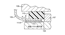
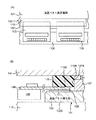
従来、図4(A),(B)に示すように、液晶パネル101のパネル電極端子102は、異方性導電フィルム103を介してテープキャリヤパッケージ(以下、TCPという)105に接続されている。このTCP105は、プリント基板106に接続されている。
【0003】
一方、上記液晶パネル101の表示部107に対向するように、バックライトパネル108が配置されている。そして、このバックライトパネル108と上記TCP105との間に防湿性樹脂からなるスペーサ110が配置されている。このスペーサ110は、表示部107とバックライトパネル108との間に所定の隙間S1を形成している。また、このスペーサ110は、内周側端面110Aが表示部外周面107Aに当接しており、底面110Bが異方性導電フィルム103とTCP105との接続部111を覆っている。なお、この接続部111は、上記パネル電極端子102の表面102Aに配置されるベゼル112と上記バックライトパネル108とで挟まれており、バックライトパネル108とベゼル112はスペーサ110に圧力を加えている。この構成により、接続部111の機械的強度を向上させている。
【0004】
また、上記スペーサ110は、外部から表示部107および接続部111にゴミや水分が侵入することを防止し、接続部111の腐食,表示部107の劣化を防止している。
【0005】
【発明が解決しようとする課題】
しかし、上記従来の液晶表示装置は、図3に示すように、接続部111がスペーサ110よりも外側にはみ出しているので、TCP105が折り曲げられると、接続部111のエッジ111Aに、TCP105を異方性導電フィルム103から引き剥がす方向(矢印Aで示す方向)の応力が集中する。このため、TCP105が異方性導電フィルム103から剥がれ易くなるという問題がある。
【0006】
そこで、この発明の目的は、パネル電極端子とTCPとの接続部および表示部へ外部から溶剤,水分,ゴミが侵入することを防止できる上に、接続部の機械的強度も向上させることができ、外力が加わったときに接続部でTCPが剥がれることを防げる液晶表示装置を提供することにある。
【0007】
【課題を解決するための手段】
上記目的を達成するため、請求項1の発明は、液晶パネルの表示部周囲の端子部が接続されたテープキャリヤパッケージと、上記液晶パネルの上記端子部に対向するバックライトパネルまたはベゼルと上記テープキャリヤパッケージとの間に挟まれて、上記液晶パネルの表示部と上記バックライトパネルまたはベゼルとの間に隙間を形成するスペーサとを備えている液晶表示装置において、
上記スペーサは、上記液晶パネルの端子部とテープキャリヤパッケージとの接続部の略全域を覆って、上記接続部の外縁よりも外方に突出しており、
かつ、上記テープキャリヤパッケージは、上記スペーサのエッジで上記接続部とは反対の方向に屈曲していることを特徴としている。
【0008】
この請求項1の発明では、上記スペーサは、図2に示すように、液晶パネルの端子部とテープキャリヤパッケージとの接続部の略全域を覆っており、上記接続部の外縁よりも外方に突出している。したがって、▲1▼TCPの曲がり始めが、接続部エッジからスペーサエッジに変わり、▲2▼接続部にかかる力の方向を90°変える。したがって、上記接続部の外縁への応力集中を抑えて、テープキャリヤパッケージが端子部から剥がれるのを防止できる。また、上記スペーサは、バックライトパネルまたはベゼルと上記テープキャリヤパッケージとの間に挟まれた状態で、上記接続部の略全域を覆っているので、接続部および表示部へ、溶剤,水分,ゴミが侵入することを防止できる。
【0009】
また、請求項2の発明は、請求項1に記載の液晶表示装置において、上記スペーサは、弾性材料からなることを特徴としている。
【0010】
この請求項2の発明では、スペーサが弾性材料で構成されているから、外からの衝撃をスペーサで吸収でき、耐衝撃性を向上できる。
【0011】
また、請求項3の発明は、請求項1または2に記載の液晶表示装置において、上記スペーサを硬質樹脂で作製したことを特徴としている。
【0012】
この請求項3の発明では、スペーサを硬質樹脂で作製したから、装置全体の機械的強度が上昇して、変形が起こり難くなり、したがって、接続部の接続不良が起こり難くなる。
【0013】
【発明の実施の形態】
以下、この発明を図示の実施の形態により詳細に説明する。
【0014】
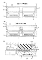
図1(A)に、この発明の液晶表示装置の実施形態を、液晶パネル1の表示面1A側から見た様子を示す。この液晶表示装置は、図1(C)に示すように、液晶パネル1の表示部2周囲の端子部3が異方性導電フィルム5を介してテープキャリヤパッケージ6に接続されている。このテープキャリヤパッケージ6は外側に延在していて、外周部6Aがプリント基板7に接続されている。
【0015】
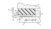
一方、上記液晶パネル1の端子部3とで上記TCP6を挟むベゼル8が配置されており、このベゼル8とTCP6との間にスペーサ10が配置されている。このスペーサ10は、弾性材料で構成されており、TCP6と異方性導電フィルム5と端子部3との接続部11の全域を覆っている。また、このスペーサ10の内周側端面10Bは、表示部2の外周面2Aに密着している。このスペーサ10によって、表示部2とベゼル8との間に所定の隙間G1を形成している。この実施形態では、図1(C),図2に示すように、スペーサ10が液晶パネル1の端子部3とTCP6との接続部11の全域を覆っており、接続部11の外縁11Aよりも外方に突出している。
したがって、▲1▼TCP6の曲がり始めが、接続部11の外縁11Aからスペーサ10のエッジ10Aに変わり、▲2▼接続部11にかかる力の方向を90°変える(矢印Bの方向)。したがって、上記接続部11の外縁11Aへの応力集中を抑えて、テープキャリヤパッケージ6が端子部3から剥がれるのを防止できる。したがって、接続部11の外縁11Aへの応力集中を抑制して、TCP6が端子部3,異方性導電フィルム5から剥がれるのを防止できる。また、上記スペーサ10は、ベゼル8とTCP6との間に挟まれた状態で、接続部11の全域を覆っているので、接続部11および表示部2へ、溶剤,水分,ゴミが侵入することを防止できる。
【0016】
また、上記スペーサ10は弾性材料で構成されているので、外からの衝撃をこのスペーサ10で吸収でき、耐衝撃性を向上できる。また、上記スペーサ10を硬度が比較的高い硬質樹脂(例えば、硬度70のシリコン樹脂)で作製したから、装置全体の機械的強度を上昇させることができる。
【0017】
尚、上記実施形態では、端子部3を異方性導電フィルム5を介してテープキャリヤパッケージ6に電気的に接続したが、端子部3をヒートシールでもってテープキャリヤパッケージ6に電気的に接続してもよい。もっとも、異方性導電フィルム5を用いた方が狭い接続面積でもって導電性を確保できる。
【0018】
上記実施形態において、ベゼル8をバックライトパネルに置き換えてもよい。この場合、ベゼルは液晶パネル端子部の表面1Aに接して配置され、バックライトパネルとベゼルとで接続部を挟むようにする。
【0019】
また、図1(B)に示すように、バックライトパネルからベゼルに向かって延在していているリブ21がTCP6,6間に有る場合にも本発明を適用できる。このリブ21は、バックライトパネルまたはベゼルから厚さ方向に延在しており、バックライトパネルとベゼルとの間隙を保つ役割を有し、組立時の位置合わせにも用いられる。この場合は、TCP6,6間のリブ21をよける凹部23をスペーサ10に形成すればよい。
【0020】
【発明の効果】
以上より明らかなように、請求項1の発明は、スペーサが、液晶パネルの端子部とテープキャリヤパッケージとの接続部の略全域を覆っており、接続部の外縁よりも外方に突出している。したがって、▲1▼TCPの曲がり始めが、接続部エッジからスペーサエッジに変わり(モジュール機構の位置関係による)、▲2▼接続部にかかる力の方向を90°変える。したがって、上記接続部の外縁への応力集中を抑えて、テープキャリヤパッケージが端子部から剥がれるのを防止できる。また、上記スペーサは、バックライトパネルまたはベゼルとテープキャリヤパッケージとの間に挟まれた状態で、接続部の略全域を覆っているので、接続部および表示部へ、溶剤,水分,ゴミが侵入することを防止できる。
【0021】
また、請求項2の発明は、スペーサが弾性材料で構成されているから、外からの衝撃をスペーサで吸収でき、耐衝撃性を向上できる。
【0022】
また、請求項3の発明では、スペーサを硬質樹脂で作製したから、装置全体の機械的強度が上昇して、変形が起こり難くなり、したがって、接続部の接続不良が起こり難くなる。
【図面の簡単な説明】
【図1】図1(A)はこの発明の液晶表示装置の実施形態の平面図であり、図1(B)は上記実施形態の変形例の平面図であり、図1(C)は上記実施形態を側方から見た様子を示す断面図である。
【図2】上記実施形態の接続部に加わる力を示している断面図である。
【図3】従来の液晶表示装置において、接続部に加わる力を示している断面図である。
【図4】図4(A)は上記従来の液晶表示装置の平面図であり、図4(B)の断面図である。
【符号の説明】
1…液晶パネル、1A…表示面、2…表示部、2A…外周面、3…端子部、
5…異方性導電フィルム、6…テープキャリヤパッケージ、6A…外周部、
7…プリント基板、8…ベゼル、10…スペーサ、10B…内周側端面、
11…接続部、G1…隙間。[0001]
BACKGROUND OF THE INVENTION
The present invention relates to a liquid crystal display device, and more particularly to a liquid crystal display device capable of improving the mechanical strength of a connection portion between a terminal portion of a liquid crystal panel and a tape carrier package.
[0002]
[Prior art]
Conventionally, as shown in FIGS. 4A and 4B, the
[0003]
On the other hand, a
[0004]
Further, the
[0005]
[Problems to be solved by the invention]
However, in the above conventional liquid crystal display device, as shown in FIG. 3, since the connecting portion 111 protrudes outside the
[0006]
Accordingly, an object of the present invention is to prevent the entry of solvent, moisture, and dust from the outside into the connection portion and display portion between the panel electrode terminal and the TCP, and to improve the mechanical strength of the connection portion. Another object of the present invention is to provide a liquid crystal display device capable of preventing TCP from being peeled off at a connection portion when an external force is applied.
[0007]
[Means for Solving the Problems]
In order to achieve the above object, a first aspect of the present invention is a tape carrier package to which terminal portions around a display portion of a liquid crystal panel are connected, a backlight panel or bezel facing the terminal portions of the liquid crystal panel, and the tape. In a liquid crystal display device provided with a spacer that is sandwiched between a carrier package and forms a gap between the display unit of the liquid crystal panel and the backlight panel or the bezel.
Said spacer covers substantially the entire area of the connection portion of the terminal portion of the upper Symbol liquid crystal panel and a tape carrier package protrudes outward from the outer edge of the connecting section,
And the tape carrier package is characterized in that bent in the direction opposite to the connecting portion and at the edge of the spacer.
[0008]
In the first aspect of the invention, as shown in FIG. 2, the spacer covers substantially the entire area of the connection portion between the terminal portion of the liquid crystal panel and the tape carrier package, and is located outward from the outer edge of the connection portion. It protrudes. Therefore, (1) the start of bending of TCP changes from the connection portion edge to the spacer edge, and (2) the direction of the force applied to the connection portion changes by 90 °. Therefore, the stress concentration on the outer edge of the connecting portion can be suppressed, and the tape carrier package can be prevented from peeling off from the terminal portion. In addition, since the spacer covers substantially the entire area of the connecting portion in a state of being sandwiched between the backlight panel or bezel and the tape carrier package, solvent, moisture, dust, etc. are applied to the connecting portion and the display portion. Can be prevented from entering.
[0009]
According to a second aspect of the invention, in the liquid crystal display device according to the first aspect, the spacer is made of an elastic material.
[0010]
In the second aspect of the present invention, since the spacer is made of an elastic material, it is possible to absorb an impact from the outside with the spacer and to improve the impact resistance.
[0011]
According to a third aspect of the present invention, in the liquid crystal display device according to the first or second aspect, the spacer is made of a hard resin.
[0012]
In the third aspect of the present invention, since the spacer is made of a hard resin, the mechanical strength of the entire apparatus is increased, and deformation is unlikely to occur.
[0013]
DETAILED DESCRIPTION OF THE INVENTION
Hereinafter, the present invention will be described in detail with reference to the illustrated embodiments.
[0014]
FIG. 1A shows a liquid crystal display device according to an embodiment of the present invention as viewed from the display surface 1 </ b> A side of the liquid crystal panel 1. In this liquid crystal display device, as shown in FIG. 1C, terminal portions 3 around the display portion 2 of the liquid crystal panel 1 are connected to a
[0015]
On the other hand, a
Accordingly, (1) the start of bending of the
[0016]
Further, since the
[0017]
In the above embodiment, the terminal portion 3 is electrically connected to the
[0018]
In the above embodiment, the
[0019]
Further, as shown in FIG. 1B, the present invention can also be applied to the case where the
[0020]
【The invention's effect】
As is clear from the above, in the invention of claim 1, the spacer covers substantially the entire area of the connection portion between the terminal portion of the liquid crystal panel and the tape carrier package, and protrudes outward from the outer edge of the connection portion. . Therefore, (1) the start of bending of TCP changes from the connection portion edge to the spacer edge (depending on the positional relationship of the module mechanism), and (2) the direction of the force applied to the connection portion changes by 90 °. Therefore, the stress concentration on the outer edge of the connecting portion can be suppressed, and the tape carrier package can be prevented from peeling off from the terminal portion. In addition, since the spacer covers almost the entire area of the connection part while being sandwiched between the backlight panel or bezel and the tape carrier package, solvent, moisture, and dust enter the connection part and the display part. Can be prevented.
[0021]
In the invention according to claim 2, since the spacer is made of an elastic material, an impact from the outside can be absorbed by the spacer, and the impact resistance can be improved.
[0022]
In the third aspect of the invention, since the spacer is made of a hard resin, the mechanical strength of the entire apparatus is increased, and deformation is unlikely to occur.
[Brief description of the drawings]
FIG. 1A is a plan view of an embodiment of a liquid crystal display device of the present invention, FIG. 1B is a plan view of a modification of the embodiment, and FIG. It is sectional drawing which shows a mode that embodiment was seen from the side.
FIG. 2 is a cross-sectional view showing a force applied to a connection portion of the embodiment.
FIG. 3 is a cross-sectional view showing a force applied to a connection portion in a conventional liquid crystal display device.
4A is a plan view of the conventional liquid crystal display device, and is a cross-sectional view of FIG. 4B. FIG.
[Explanation of symbols]
DESCRIPTION OF SYMBOLS 1 ... Liquid crystal panel, 1A ... Display surface, 2 ... Display part, 2A ... Outer peripheral surface, 3 ... Terminal part,
5 ... anisotropic conductive film, 6 ... tape carrier package, 6A ... outer periphery,
7 ... Printed circuit board, 8 ... Bezel, 10 ... Spacer, 10B ... End surface on the inner circumference side,
11: Connection portion, G1: Gap.
Claims (3)
上記スペーサは、上記液晶パネルの端子部とテープキャリヤパッケージとの接続部の略全域を覆って、上記接続部の外縁よりも外方に突出しており、
かつ、上記テープキャリヤパッケージは、上記スペーサのエッジで上記接続部とは反対の方向に屈曲していることを特徴とする液晶表示装置。A tape carrier package to which a terminal portion around the display portion of the liquid crystal panel is connected, and a backlight panel or bezel facing the terminal portion of the liquid crystal panel and the tape carrier package. In a liquid crystal display device including a spacer that forms a gap between the display unit and the backlight panel or the bezel,
Said spacer covers substantially the entire area of the connection portion of the terminal portion of the upper Symbol liquid crystal panel and a tape carrier package protrudes outward from the outer edge of the connecting section,
And the tape carrier package, a liquid crystal display device characterized by being bent in the direction opposite to the above-mentioned connection portions at the edge of the spacer.
上記スペーサは、弾性材料からなることを特徴とする液晶表示装置。The liquid crystal display device according to claim 1.
The liquid crystal display device, wherein the spacer is made of an elastic material.
上記スペーサを硬質樹脂で作製したことを特徴とする液晶表示装置。The liquid crystal display device according to claim 1 or 2,
A liquid crystal display device, wherein the spacer is made of a hard resin.
Priority Applications (1)
| Application Number | Priority Date | Filing Date | Title |
|---|---|---|---|
| JP14096598A JP3607076B2 (en) | 1998-05-22 | 1998-05-22 | Liquid crystal display |
Applications Claiming Priority (1)
| Application Number | Priority Date | Filing Date | Title |
|---|---|---|---|
| JP14096598A JP3607076B2 (en) | 1998-05-22 | 1998-05-22 | Liquid crystal display |
Publications (2)
| Publication Number | Publication Date |
|---|---|
| JPH11338368A JPH11338368A (en) | 1999-12-10 |
| JP3607076B2 true JP3607076B2 (en) | 2005-01-05 |
Family
ID=15280946
Family Applications (1)
| Application Number | Title | Priority Date | Filing Date |
|---|---|---|---|
| JP14096598A Expired - Fee Related JP3607076B2 (en) | 1998-05-22 | 1998-05-22 | Liquid crystal display |
Country Status (1)
| Country | Link |
|---|---|
| JP (1) | JP3607076B2 (en) |
Families Citing this family (2)
| Publication number | Priority date | Publication date | Assignee | Title |
|---|---|---|---|---|
| KR100626015B1 (en) | 2004-09-08 | 2006-09-20 | 삼성에스디아이 주식회사 | Flat panel display panel and flat panel display device having same |
| JP7776966B2 (en) | 2021-11-01 | 2025-11-27 | シャープ株式会社 | display device |
-
1998
- 1998-05-22 JP JP14096598A patent/JP3607076B2/en not_active Expired - Fee Related
Also Published As
| Publication number | Publication date |
|---|---|
| JPH11338368A (en) | 1999-12-10 |
Similar Documents
| Publication | Publication Date | Title |
|---|---|---|
| US8259250B2 (en) | Liquid crystal display apparatus and method for grounding liquid crystal display apparatus | |
| JP2007193275A (en) | Liquid crystal display device and manufacturing method thereof | |
| US4767189A (en) | Terminal connection structure for a liquid crystal display device | |
| JP3607076B2 (en) | Liquid crystal display | |
| JPH05188388A (en) | Liquid crystal display | |
| JP2000155306A (en) | Display device | |
| JPH11119680A (en) | Liquid crystal display | |
| JP3678918B2 (en) | Liquid crystal display device, holding member for liquid crystal display device, and assembly structure of liquid crystal display device | |
| JP2001265239A (en) | Display device | |
| JPH09199875A (en) | Liquid crystal display | |
| JPH1048599A (en) | Liquid crystal display | |
| JP2573812B2 (en) | Liquid crystal display device and method of manufacturing the same | |
| EP1220017B1 (en) | Portable apparatus with flexible film liquid crystal display device | |
| JPH08313880A (en) | Liquid crystal display device and its production | |
| JP3103501B2 (en) | Manufacturing method of liquid crystal element | |
| JP2982736B2 (en) | Liquid crystal display | |
| US20060132695A1 (en) | Liquid crystal display device and mobile communication | |
| JPH08271863A (en) | Circuit board and display device | |
| JP3349365B2 (en) | Liquid crystal display device and method of manufacturing the same | |
| JP3691303B2 (en) | Electronic timepiece having a coil block protection structure | |
| CN209514239U (en) | A kind of display device | |
| JPH01142534A (en) | Display device | |
| JP2011008110A (en) | Holding structure for display panel, and display device | |
| JPH10288771A (en) | Liquid crystal display device | |
| JP2005017890A (en) | Liquid crystal display device |
Legal Events
| Date | Code | Title | Description |
|---|---|---|---|
| A131 | Notification of reasons for refusal |
Free format text: JAPANESE INTERMEDIATE CODE: A131 Effective date: 20040511 |
|
| A521 | Written amendment |
Free format text: JAPANESE INTERMEDIATE CODE: A523 Effective date: 20040706 |
|
| TRDD | Decision of grant or rejection written | ||
| A01 | Written decision to grant a patent or to grant a registration (utility model) |
Free format text: JAPANESE INTERMEDIATE CODE: A01 Effective date: 20040928 |
|
| A61 | First payment of annual fees (during grant procedure) |
Free format text: JAPANESE INTERMEDIATE CODE: A61 Effective date: 20041006 |
|
| R150 | Certificate of patent (=grant) or registration of utility model |
Free format text: JAPANESE INTERMEDIATE CODE: R150 |
|
| FPAY | Renewal fee payment (prs date is renewal date of database) |
Free format text: PAYMENT UNTIL: 20071015 Year of fee payment: 3 |
|
| FPAY | Renewal fee payment (prs date is renewal date of database) |
Free format text: PAYMENT UNTIL: 20081015 Year of fee payment: 4 |
|
| FPAY | Renewal fee payment (prs date is renewal date of database) |
Free format text: PAYMENT UNTIL: 20081015 Year of fee payment: 4 |
|
| FPAY | Renewal fee payment (prs date is renewal date of database) |
Free format text: PAYMENT UNTIL: 20091015 Year of fee payment: 5 |
|
| FPAY | Renewal fee payment (prs date is renewal date of database) |
Free format text: PAYMENT UNTIL: 20091015 Year of fee payment: 5 |
|
| FPAY | Renewal fee payment (prs date is renewal date of database) |
Free format text: PAYMENT UNTIL: 20101015 Year of fee payment: 6 |
|
| FPAY | Renewal fee payment (prs date is renewal date of database) |
Free format text: PAYMENT UNTIL: 20111015 Year of fee payment: 7 |
|
| FPAY | Renewal fee payment (prs date is renewal date of database) |
Free format text: PAYMENT UNTIL: 20121015 Year of fee payment: 8 |
|
| FPAY | Renewal fee payment (prs date is renewal date of database) |
Free format text: PAYMENT UNTIL: 20131015 Year of fee payment: 9 |
|
| LAPS | Cancellation because of no payment of annual fees |