JP3607026B2 - Digital PLL circuit - Google Patents
Digital PLL circuit Download PDFInfo
- Publication number
- JP3607026B2 JP3607026B2 JP35106296A JP35106296A JP3607026B2 JP 3607026 B2 JP3607026 B2 JP 3607026B2 JP 35106296 A JP35106296 A JP 35106296A JP 35106296 A JP35106296 A JP 35106296A JP 3607026 B2 JP3607026 B2 JP 3607026B2
- Authority
- JP
- Japan
- Prior art keywords
- circuit
- delay
- frequency
- clock signal
- variable
- Prior art date
- Legal status (The legal status is an assumption and is not a legal conclusion. Google has not performed a legal analysis and makes no representation as to the accuracy of the status listed.)
- Expired - Fee Related
Links
Images


Classifications
-
- H—ELECTRICITY
- H03—ELECTRONIC CIRCUITRY
- H03L—AUTOMATIC CONTROL, STARTING, SYNCHRONISATION OR STABILISATION OF GENERATORS OF ELECTRONIC OSCILLATIONS OR PULSES
- H03L7/00—Automatic control of frequency or phase; Synchronisation
- H03L7/06—Automatic control of frequency or phase; Synchronisation using a reference signal applied to a frequency- or phase-locked loop
- H03L7/08—Details of the phase-locked loop
- H03L7/081—Details of the phase-locked loop provided with an additional controlled phase shifter
- H03L7/0812—Details of the phase-locked loop provided with an additional controlled phase shifter and where no voltage or current controlled oscillator is used
- H03L7/0814—Details of the phase-locked loop provided with an additional controlled phase shifter and where no voltage or current controlled oscillator is used the phase shifting device being digitally controlled
-
- H—ELECTRICITY
- H03—ELECTRONIC CIRCUITRY
- H03K—PULSE TECHNIQUE
- H03K5/00—Manipulating of pulses not covered by one of the other main groups of this subclass
- H03K5/13—Arrangements having a single output and transforming input signals into pulses delivered at desired time intervals
- H03K5/133—Arrangements having a single output and transforming input signals into pulses delivered at desired time intervals using a chain of active delay devices
-
- H—ELECTRICITY
- H03—ELECTRONIC CIRCUITRY
- H03L—AUTOMATIC CONTROL, STARTING, SYNCHRONISATION OR STABILISATION OF GENERATORS OF ELECTRONIC OSCILLATIONS OR PULSES
- H03L7/00—Automatic control of frequency or phase; Synchronisation
- H03L7/06—Automatic control of frequency or phase; Synchronisation using a reference signal applied to a frequency- or phase-locked loop
- H03L7/08—Details of the phase-locked loop
- H03L7/085—Details of the phase-locked loop concerning mainly the frequency- or phase-detection arrangement including the filtering or amplification of its output signal
- H03L7/087—Details of the phase-locked loop concerning mainly the frequency- or phase-detection arrangement including the filtering or amplification of its output signal using at least two phase detectors or a frequency and phase detector in the loop
-
- H—ELECTRICITY
- H03—ELECTRONIC CIRCUITRY
- H03L—AUTOMATIC CONTROL, STARTING, SYNCHRONISATION OR STABILISATION OF GENERATORS OF ELECTRONIC OSCILLATIONS OR PULSES
- H03L2207/00—Indexing scheme relating to automatic control of frequency or phase and to synchronisation
- H03L2207/50—All digital phase-locked loop
Landscapes
- Physics & Mathematics (AREA)
- Nonlinear Science (AREA)
- Stabilization Of Oscillater, Synchronisation, Frequency Synthesizers (AREA)
- Networks Using Active Elements (AREA)
- Pulse Circuits (AREA)
Description
【0001】
【発明の属する技術分野】
本発明はディジタルPLL回路に関し、特に複雑な制御アルゴリズムを必要とせずに低ジッタと高精度を提供できるように周波数比較回路を有するディジタルPLL回路に関する。
【0002】
【従来の技術】
フェーズ・ロックド・ループ(PLL)回路は、広い分野で用いられており、集積化に適したいかなる分野にも用いることができる。特に、PLL回路は、AM・FMラジオ、テレビ、無線通信等、周波数シンセサイザ、マルチプレクス・ステレオ復調回路等の各種信号回路に用いられている。
【0003】
一般に、PLL回路は可変発振器により発生された周波数と位相が基準信号のそれらにロックされるようなフィードバックループである。PLL回路は周波数変調された搬送波の中からベースバンド信号を復調するために用いられる。基本的なPLL回路は位相比較回路と電圧制御発振器とを備えている。動作においては、変調された入力信号と電圧制御発振器の出力とが位相比較回路によって比較され、この位相比較回路の出力によって電圧制御発振器の周波数が制御される。
図14は、従来のディジタルPLL回路のブロック構成図である。同図に示されるように、基準クロック信号が位相比較器74に入力され、位相比較器74の出力はディレイ制御回路73に与えられる。ディレイ可変回路76はディレイ制御回路73の出力を受け取り、ディレイ可変回路76の出力はインバータ77に与えられる。インバータ77の出力はディレイ可変回路76にフィードバックされ、ディレイ可変回路76及びインバータ77によってリング・オシレータが構成されている。
【0004】
リング・オシレータの出力信号(すなわち、インバータの出力信号)は出力クロック信号として用いられる一方、位相比較器74へ入力され、基準クロック信号と位相を比較される。ディレイ制御回路73は、位相比較器74からの位相比較出力を基にして基準クロック信号の位相と、出力クロック信号の位相とが一致するようにディレイ可変回路76を制御する。
【0005】
典型的には、ディレイ可変回路76は、通常、インバータ列で構成されており、その接続段数を変更することによりディレイ値を変更する。しかし、インバータの接続段数の変更のみでディレイ値を制御すると、制御可能なディレイ値の刻みが粗い。もし、可変負荷容量回路(キャパシタを含む)がインバータの出力側に接続されるならば、インバータに接続されるキャパシタの個数を変更することにより、インバータの出力負荷容量を変更することができる。このことは、ディレイ値のより高精度の制御と、より精度の高いディジタルPLL回路を得ることができる。このような回路では、ディレイ制御回路73は、位相比較器74からの位相比較出力を基にディレイ可変回路76のインバータの接続段数及び出力負荷容量を制御している。
【0006】
【発明が解決しようとする課題】
しかしながら、上述した従来のディジタルPLL回路においては、ディレイ可変回路76の出力負荷容量によるより高精度な制御を行った場合であっても、ディレイ制御回路73の制御を位相比較出力によって行っているため、PLLとしてロックするようにディレイ制御回路73を設計することが非常に困難であるという問題点がある。
【0007】
例えば、出力クロック信号の周波数が基準クロック信号の周波数と一致していた場合でも、出力クロック信号の位相が基準クロック信号の位相より遅れていたときは、位相比較器74の出力に基づきディレイ制御回路73はディレイ可変回路76のディレイ値を減少させるように動作する。多くの場合、位相を一致させるべく、この動作を幾度か繰り返した後には多くの場合、逆に周波数が不一致となる。したがって、ディレイ制御回路73は今度は周波数を一致させるべく動作する。この結果、競合する動作の繰り返しとなって、周波数と位相とがともに一致するまでには多くの無駄な動作が含まれて所要時間も長くなる。
【0008】
以上のように、従来のディジタルPLL回路、特に出力クロック信号と基準クロック信号の位相及び周波数を一致させられるようなディレイ制御回路の設計は困難である。この結果、従来の設計は複雑な構成とディレイ制御回路を制御するための非常に複雑な制御用アルゴリズムを含むこととなる。また、従来のディジタルPLL回路はPLL回路が一度ロックした後でもわずかに位相がずれただけで、ディレイ制御回路はディレイ可変回路のディレイ値を変更するように動作し、その結果、出力クロック信号の周波数も変更され信号のジッタが大きくなるという問題もある。
【0009】
本発明は上記問題点に鑑みてなされたもので、その目的は、複雑な制御用アルゴリズムが不要で設計及び制御が容易な、ジッタの小さい高精度のディジタルPLL回路を提供することである。
【0010】
【課題を解決するための手段】
本発明に係るディジタルPLL回路の第1の態様によれば、
出力クロック信号の周波数と基準クロック信号の周波数とを比較し、周波数比較情報を発生する周波数比較回路と、
前記出力クロック信号の位相と前記基準クロック信号の位相とを比較し、位相比較情報を発生する位相比較回路と、
前記出力クロック信号の周波数についての前記周波数比較情報と、前記出力クロック信号の位相についての前記位相比較情報に基づいて、ディレイ可変用ディジタル信号を発生するディレイ制御回路と、
前記ディレイ制御回路の出力により前記基準クロック信号の周波数および位相にロックされるような出力クロック信号を発生する可変周波数発振器と、
を備え
前記位相比較情報によるディレイ変化量は、前記周波数比較情報により決定したディレイ制御情報に対して単位ディレイ量を増加もしくは減少させるものであることを特徴とする。
【0011】
本発明に係るディジタルPLL回路の第2の態様によれば、
出力クロック信号を分周し、分周出力クロック信号を発生する第1の分周回路と、
基準クロック信号を分周し、分周基準クロック信号を発生する第2の分周回路と、
前記分周出力クロック信号の周波数と前記分周基準クロック信号の周波数とを比較し、周波数比較情報を発生する周波数比較回路と、
前記分周出力クロック信号の位相と前記分周基準クロック信号の位相とを比較し、位相比較情報を発生する位相比較回路と、
前記出力クロック信号の周波数についての前記周波数比較情報と、前記出力クロック信号の位相についての前記位相比較情報に基づいて、ディレイ可変用ディジタル信号を発生するディレイ制御回路と、
前記出力クロック信号を発生する可変周波数発振器を備え、
前記出力クロック信号の周波数および位相の制御は前記周波数比較情報と前記位相比較情報に基づいて行われ、前記可変周波数発振器は出力クロック信号を基準クロック信号の周波数のN/M倍(ただし、Mは前記第2の分周回路における基準クロック信号に対する周波数分割比、Nは前記第1の分周回路におけるディレイ可変回路の出力信号に対する周波数分割比であって、いずれも自然数)の周波数に位相ロックして出力し、
前記位相比較情報によるディレイ変化量は、前記周波数比較情報により決定したディレイ制御情報に対して単位ディレイ量を増加もしくは減少させるものであることを特徴とする。
【0012】
本発明に係るディジタルPLL回路の第3の態様によれば、
基準クロックと出力クロックを比較する比較手段と、
前記比較手段からの比較情報をもとに負荷容量制御情報を発生させる負荷容量制御回路と、
前記負荷容量制御回路からの負荷容量制御情報をもとにディレイ値可変なディレイ可変回路を含み、所望の出力クロック信号を出力するクロック信号発生回路とを備え、
前記ディレイ可変回路は前記負荷容量制御回路からの負荷容量制御情報をMOSトランジスタのソースもしくはドレインに接続し、前記MOSトランジスタのゲートを前記ディレイ可変回路の一旦に接続した負荷容量可変回路を有することを特徴とする。
【0014】
【発明の実施の形態】
以下、本発明に係るPLLの実施の形態のいくつかにつき、図面を参照しながら説明する。
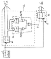
図1は、本発明に係るディジタルPLL回路の第1の実施の形態のブロック構成図である。周波数比較回路11は出力クロック信号の周波数を基準クロック信号の周波数と比較し、周波数比較情報を含む出力信号を発生する。負荷容量制御回路12は周波数比較回路11の出力を受け取り、ディレイ可変回路16の負荷容量を制御する負荷容量制御出力情報を含む出力信号を発生する。周波数比較回路11の出力はディレイ段数(ディレイ値を発生するインバータの接続段数)を制御するディレイ段数制御出力情報を発生するディレイ段数制御回路13に与えられる。
【0015】
さらに、位相比較回路14は出力クロック信号の位相と基準クロック信号の位相とを比較し位相比較出力情報を含む出力信号を発生する。
【0016】
加算/減算回路15は位相比較回路14の出力および負荷容量制御回路12の出力を受け取り、位相比較回路14からの位相比較出力情報に基づき、負荷容量制御回路12からの負荷容量制御出力情報に対しインクリメントまたはデクリメントを与え、負荷容量加算/減算制御出力情報を含む出力信号を発生する。ディレイ可変回路16はディレイ段数制御回路13の出力及び加算/減算回路15の出力を受け取り、ディレイ段数制御回路13からのディレイ段数制御出力情報に基づきディレイ段数を制御し、加算/減算回路15からの負荷容量加算/減算制御出力情報に基づき、負荷容量の加算/減算制御を行う。インバータ17はディレイ可変回路16の出力と入力との間に接続され、ディレイ可変回路16とともにリング・オシレータを構成する。
【0017】
このように、本発明では、ディレイ可変回路16のディレイ段数制御を、位相比較出力情報ではなく、周波数比較出力情報に基づいて行っている。また、ディレイ可変回路16の負荷容量可変回路の制御を行う加算/減算回路15は周波数比較出力情報を主として、位相比較出力情報を補助として制御を行う。このような特徴は、本発明の第1の実施の形態にかかるディジタルPLL回路を複雑な制御用アルゴリズムが不要で、ジッタの小さい高精度のものとしている。さらに、ディレイ可変回路16は、ディレイ値をより高精度に制御可能とするため、接続段数変更可能な複数のインバータと、接続段数変更に関わらない所定インバータの出力側に配設され、キャパシタを含む複数の負荷容量可変回路とを備え、インバータの接続段数及びインバータの出力負荷容量を制御することにより、ディレイ値をより高精度に制御することができる。
【0018】
図2は、図1に示したディレイ可変回路の好ましい実施例を示すブロック構成図である。このディレイ可変回路16は、第1の段だけ縦列接続され、接続段数変更に関わらないインバータ21及び22を含んでいる。さらに、それぞれ2つのインバータを含む2s−1 段のインバータ対23,24が選択された接続段数に基づいて選択的に用いられるように設けられている。各2s段のインバータの出力はマルチプレクサ20に、その接続段数変更を制御すべく与えられる。さらに、負荷容量可変回路Cn1〜Cnmと負荷容量可変回路Cnm+1〜Cnn(キャパシタを含む)は第1段のインバータ21および22の出力負荷容量を定めるのに用いられる。上述したように、インバータの接続段数とインバータの出力負荷容量とを共に変更することにより、ディレイ値をより高精度に制御することができる。
【0019】
図2に示されたディレイ可変回路の動作を説明する。マルチプレクサ20には、ディレイ段数制御回路13からのディレイ段数制御出力情報であるディレイ段数制御信号El1〜Ellが入力され、これらのディレイ段数制御信号El1〜Ellのディジタル値を制御することによりマルチプレクサの入力端子0〜2s−1 のうちのいずれかが選択される。マルチプレクサの入力には、上述のように、縦列接続された2s 段のインバータの出力が接続されているので、選択された段数のインバータがディレイ可変回路の出力に接続され、所定のディレイ値を発生する。したがって、ディレイ段数制御信号El1〜Ellに基づくインバータの接続段数変更により、インバータ2段(すなわち1接続段)が発生するディレイ値を一単位として、ディレイ可変回路のディレイ値を制御することができる。
【0020】
そして、さらにディレイ値を高精度に制御するために、上述のように、接続段数変更に関わらないインバータ21及び22の出力側には、各インバータの出力負荷容量となるキャパシタを含む負荷容量可変回路Cn1〜Cnmと負荷容量可変回路Cnm+1〜Cnnとが選択的に接続されている。すなわち、各負荷容量可変回路Cは、その構成の一例が負荷容量可変回路Cn1として示されるように、キャパシタ25とアナログスイッチ26とから構成されている。各負荷容量可変回路Cはそのアナログスイッチを負荷容量加算/減算制御信号Enの一つに基づいて開閉する。このように、負荷容量加算/減算制御信号は負荷容量制御回路12からの負荷容量制御情報および位相比較回路の出力に基づいて加算器/減算器回路15から出力される。
【0021】
すなわち、負荷容量加減制御信号En1〜Enm、Enm+1〜Ennの値が「1」のときは、当該信号が入力される負荷容量可変回路の対応するアナログスイッチが接続され、インバータ21、22の出力に当該負荷容量可変回路のキャパシタが接続される。逆に、負荷容量加減制御信号En1〜Enm、Enm+1〜Ennの値が「0」のときは、当該信号が入力される負荷容量可変回路の対応するアナログスイッチが開放され、インバータの出力から当該負荷容量可変回路のキャパシタが切り離される。したがって、負荷容量加減制御信号En1〜Enm、Enm+1〜Ennに基づいてインバータの出力負荷容量が加減される。これによりディレイ可変回路のディレイ値はより高精度に制御可能となる。
【0022】
図3は、ディレイ可変回路のインバータの接続段数とインバータに接続される出力負荷容量とを変更したときのディレイ値の変化を示すグラフである。そのグラフにおいて線OP2、OP4、OP6はそれぞれインバータの段数が2段、4段、6段のときのディレイ可変回路の出力信号のディレイ値である。それぞれ単調増加(厳密には、小さい階段状)のグラフとなっているのは、接続段数変更に関わらない2個のインバータの出力側に配設された複数の負荷容量可変回路によるディレイ値の高精度の制御によるものである。さらに、インバータの接続段数変更によるディレイ値の制御は、インバータ2段ごとの制御であり、かつ、複数の負荷容量可変回路によるディレイ値の調整量は、典型的にはインバータ2段分のディレイ値の量以上である。例えば、グラフOP2の右端とグラフOP4の左端、グラフOP4の右端とグラフOP6の左端とはそれぞれディレイ値が連続、または一部重複するようになっている。このように、本発明の第1の実施の形態にかかるディレイ可変回路は連続した高精度のディレイ値の制御を可能とする。
以下、図1および図2のディジタルPLL回路全体の動作について説明する。最初に、出力クロック信号と基準クロック信号の周波数を一致させるディジタルPLLの動作につき説明する。
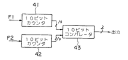
図4は、図1における周波数比較回路11の一例のブロック構成図である。図4に示すように、2つのクロック信号F1およびF2がそれぞれ2個の10ビットカウンタ41及び42に与えられる。10ビットコンパレータ43はこれらのカウンタの出力を受ける。2個の10ビットカウンタ41及び42は、基準クロック信号F1のクロック数とディジタルPLL回路出力クロック信号F2のクロック数とをそれぞれカウントし、いずれかのカウンタがが10ビットをフルカウント(すなわち210)した時に両方の10ビットカウンタは停止される。2個のカウンタのカウント出力はレジスタ回路に記憶され、コンパレータ43によって比較される。好ましい実施例ではレジスタ回路は各カウンタに含まれる。比較結果は周波数比較出力情報として周波数比較回路11から出力される。この実施の形態においては、周波数比較回路11はいずれのカウント値が大きいか、一致するかを示す3ビット信号(例えば常に1つの「1」と2つの「0」を持つ信号)を出力する。
【0023】
周波数比較情報に応答して、負荷容量制御回路12およびディレイ段制御回路13は負荷容量制御信号E’nおよびディレイ段制御信号Esをそれぞれ出力する。図6は図1における負荷容量制御回路12およびディレイ制御回路13の好ましい実施例のブロック図を示す。図示されたように、第1のアップダウンカウンタ81は周波数比較回路11から周波数比較情報を受け取る。第1のアップダウンカウンタ81の出力E’nはイネーブル論理回路82および加算/減算回路15に与えられる。イネーブル論理回路82は第1のアップダウンカウンタ81の出力がすべて「1」であり出力クロック信号F2の周波数が基準クロック信号F1の周波数よりも高いときか、第1のアップダウンカウンタ81の出力がすべて「0」であり出力クロック信号F2の周波数が基準クロック信号F1の周波数よりも低いときのいずれかの場合にイネーブル信号ECを発生する。図6の例では、加算/減算回路15は負荷容量加算/減算制御信号Enを発生するデコーダを含んでいる。他の例では、デコーダは負荷容量制御回路12に含まれる。さらに、ディレイ段制御回路13はイネーブル信号を負荷容量制御回路12から、周波数比較情報を周波数比較回路11からそれぞれ受け取る第2のアップダウンカウンタ88を含む。この第2のアップダウンカウンタ88の出力Esはディレイ可変回路16に与えられる。
【0024】
より詳しく述べると、周波数比較回路が出力クロック信号の周波数が基準クロック信号の周波数より高いことを示したときは、負荷容量制御回路12は、負荷容量制御出力信号E’n1〜E’nmの数を1つ増加させる。すなわち、負荷容量制御出力信号E’n1〜E’nmのうち「1」の状態にある信号の個数を1個増加させる。これにより、インバータに接続されるキャパシタが一個増加してインバータの出力負荷容量がわずかに増加し、ディジタルPLL回路出力クロック信号の周波数がわずかに低下する方向に作用する。次の周波数比較時に、キャパシタを1個接続してもなおディジタルPLL回路出力クロック信号の周波数が基準クロック信号の周波数より高いときは、爾後の周波数比較時に上述したと同様に負荷容量制御出力信号E’n1〜E’nnのうち「1」の状態にある信号の個数をさらに1個増加させる。この動作は、ディジタルPLL回路出力クロック信号と基準クロック信号の周波数が等しくなるまで繰り返される。
【0025】
負荷容量制御出力信号E’n1〜E’nnのすべてが「1」となった後もディジタルPLL回路出力クロック信号の周波数が基準クロック信号の周波数より高いときは、爾後の周波数比較時に負荷容量制御出力信号E’n1〜E’nnをすべてリセットして「0」とし、同時にこのリセット情報をディレイ段数制御回路13に対して出力する。
【0026】
ディレイ段数制御回路13においては、負荷容量制御回路12からのリセット情報に基づき、ディレイ段数制御出力情報であるディレイ段数制御信号Esをインクリメントする。これにより、ディレイ可変回路16のインバータの接続段数は2段増加する(すなわち、さらに1段の接続が用いられる)。上述のように、負荷容量制御回路12およびディレイ段数制御回路13は出力クロック信号と基準クロック信号とが一致するまで動作を続ける。負荷容量可変回路によるディレイ値の制御の幅は、通常、インバータ2段分のディレイ値の幅以上とされているため、連続したディレイ値の高精度の制御が可能となる。
【0027】
以上のように、本発明の第1の実施の形態によれば、インバータの接続段数とインバータの出力負荷容量を順次増加させることにより、ディジタルPLL回路出力クロック信号の周波数は基準クロック信号の周波数となるまで徐々に低下する。このようにして安定した周波数の一致が確立される。
【0028】
ディジタルPLL回路出力クロック信号の周波数が基準クロック信号の周波数より高い場合は、以上のような動作が行われるが、ディジタルPLL回路出力クロック信号の周波数が基準クロック信号の周波数より低い場合は、以上とは逆の動作を行う。すなわち、周波数比較出力情報に基づき、ディジタルPLL回路出力クロック信号の周波数が基準クロック信号の周波数より低いときは、負荷容量制御回路12はアクティブ負荷容量制御出力信号E’n1〜E’nnの数を1つ減少させるようにカウントダウンする。すなわち、負荷容量制御出力信号E’n1〜E’nnのうち「1」の状態にある信号の個数を1個減少させる。その結果、第1段インバータに接続されるキャパシタが一個減少してインバータの出力負荷容量がわずかに減少し、逆に出力クロック信号の周波数がわずかに上昇する。接続されるキャパシタを1個減少させてもなお、次の比較時にディジタルPLL回路出力クロック信号の周波数が基準クロック信号の周波数より低いときは、爾後の周波数比較時に上述したと同様に負荷容量制御出力信号E’n1〜E’nnのうち「1」の状態にある信号の個数をさらに1個減少させる。この動作は、ディジタルPLL回路出力クロック信号と基準クロック信号の周波数が等しくなるまで繰り返される。
【0029】
負荷容量制御出力信号E’n1〜E’nnのすべてが「0」となった後もディジタルPLL回路出力クロック信号の周波数が基準クロック信号の周波数より低いときは、負荷容量制御出力信号E’n1〜Ennをすべてリセットして「1」とし、同時にこのリセット情報をディレイ段数制御回路13に対して出力する。
【0030】
ディレイ段数制御回路13は、リセット情報に基づき、ディレイ段数制御出力情報であるディレイ段数制御信号Esをデクリメントする。これにより、ディレイ可変回路16のインバータの接続段数は2段減少する(すなわち、さらに1段少ない接続が用いられる)。上述のように、負荷容量制御回路12およびディレイ段数制御回路13は出力クロック信号と基準クロック信号とが一致するまで動作を続ける。
【0031】
以上のように、インバータの接続段数とインバータの出力負荷容量を順次減少させることにより、ディジタルPLL回路出力クロック信号の周波数は基準クロック信号の周波数と同じ周波数になるまで徐々に上昇する。このようにして周波数の安定な一致が確立される。
【0032】
さらに、ディレイ可変回路16とインバータ17とから構成されるリング・オシレータの発振周波数、すなわち出力クロック信号の周波数は、インバータの段数とインバータに接続される出力負荷容量とによって決定されるので、一度、ディジタルPLL回路がロックしたときは、非常に高精度の発振周波数を得ることができる。
【0033】
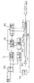
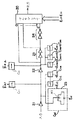
次に、図1および2のディジタルPLL回路の出力クロック信号と基準クロック信号の位相を一致させる動作(位相合わせ)について説明する。位相合わせは図1における位相比較回路14と加算/減算回路15により行われる。図5は図1の位相比較回路14の好ましい実施例を示すブロック図である。
【0034】
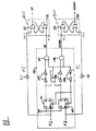
位相差検出部110の出力は第1および第2のSRフリップフロップ120および130に与えられる。位相差検出部は2つのクロック信号(F1およびF2)がそれぞれフリップフロップ101、102に与えられ、これらフリップフロップの入力端子は電源VDDに接続されている。NANDゲート104は両フリップフロップ101、102の出力を受ける。各フリップフロップ(101または102)の出力はインバータ対(103または105)を介してANDゲート107または108にも与えられる。NANDゲート104はANDゲート107および108、およびインバータ対106を介してフリップフロップ101および102のクリア端子に与えられている。
【0035】
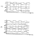
位相差検出部110のUP出力信号は、基準クロック信号F1が与えられるフリップフロップ101の出力を受けるANDゲート107から第1のSRフリップフロップ120のセット端子に与えられる。同様に、DOWN出力信号は、出力クロック信号F2が与えられるフリップフロップ102の出力を受けるANDゲート108から第2のSRフリップフロップ130のセット端子に与えられる。基準クロック信号F1は第1のSRフリップフロップ120のリセット端子にインバータ111を介して与えられ、出力クロック信号F2は第2のSRフリップフロップ130のリセット端子にインバータ112を介して与えられる。位相比較器14から位相比較情報として出力されるUP’およびDOWN’出力信号は、第1および第2のSRフリップフロップ120および130からそれぞれ供給される。各SRフリップフロップのリセット端子には反転したクロック信号の一つが与えられるので、出力信号UP’およびDOWN’は図13(b)に示されるように、2つのクロック信号間の位相差にかかわらず、それぞれのクロック信号とパルス幅が一致する。
【0036】
上述したように、位相比較回路14は出力クロック信号の位相を基準クロック信号の位相と比較し、位相比較情報を出力する。さらに詳細には、もし出力クロック信号が基準クロック信号よりも遅れているときは、位相比較回路はUP’出力信号を出力し、加算/減算回路15に、負荷容量制御回路12からの負荷容量制御出力情報E’nに対して「1」を減算させる(図13(a)(b)参照)。その結果は、ディレイ可変回路16に対して負荷容量加算/減算制御出力情報として出力されて、ディレイ可変回路16のインバータに接続されているキャパシタが1個減少し、ディジタルPLL回路出力クロック信号の位相が基準クロック信号の位相に対してわずかに進む方向に変位する。
【0037】
逆に、ディジタルPLL回路出力クロック信号の位相と基準クロック信号の位相とを比較した結果、ディジタルPLL回路出力クロック信号の位相が基準クロック信号の位相に対して進んでいたときは、位相比較回路14はDOWN’出力信号を出力し、加算/減算回路15に、負荷容量制御回路12からの負荷容量制御出力情報E’nに対して「1」を加算させる(図13(b)参照)。その結果は、ディレイ可変回路16に対して負荷容量加算/減算制御出力情報として出力されて、ディレイ可変回路16のインバータに接続されているキャパシタが1個増加し、ディジタルPLL回路出力クロック信号の位相が基準クロック信号の位相に対してわずかに遅れる方向に変位する。
【0038】
加算/減算回路15は、位相比較回路14での位相比較の結果に基づき、単に、負荷容量制御回路12からの負荷容量制御出力情報に対して「1」の加算動作または減算動作を繰り返すのみである。したがって、加算動作または減算動作を行った結果に基づいて爾後の位相比較を行い、負荷容量制御出力情報に対して「1」の加算または減算をした結果の情報に対してさらに加算動作または減算動作を行うことはない。言い換えれば、加算/減算回路15は、負荷容量制御情報に対する最初の「1」の加算あるいは減算による制御情報に別の加算や減算を行うことはなく、位相比較回路は負荷容量制御回路の出力を「1」だけ変更できる(すなわち、一つのキャパシタを接続あるいは切り離しできる)だけである。
【0039】
また、ディジタルPLL回路出力クロック信号の位相と基準クロック信号の位相とが一致したときには、加算/減算回路15の加算動作または減算動作は停止される。この時点では、インバータの接続段数、負荷容量ともにPLL回路の周波数がロックしたときと同じなので、リング・オシレータの発振周波数も基準クロック信号の周波数と一致する。
【0040】
本発明におけるディジタルPLL回路では、周波数比較が行われた後、出力クロック信号の周波数は位相合わせの際に若干変化させられる。詳しく述べると、「1」の加算あるいは減算が負荷容量制御情報に基づいて行われる時、出力クロック信号の周波数は、周波数整合動作によって設定される周波数からはわずかに変化する。そして、次の周波数比較は位相合わせ動作によって影響されることになる。しかしながら、周波数比較が1024クロック周期(10ビットカウンタの場合)に1回であるのに対し、位相比較は毎クロック周期に行なわれるので、負荷容量制御情報における位相合わせ動作によるいかなる変動も位相比較回路および加算/減算回路により修正される。さらに、位相比較回路は周波数比較動作(上述)により定められた負荷容量制御情報を「1」だけ変化させるものであるので、位相合わせ動作中に周波数がわずかに変動するのがせいぜいである。
【0041】
このように、本発明の第1の実施の形態では、周波数及び位相が基準クロック信号と一致したディジタルPLL回路出力クロック信号を得ることができる。すなわち、本発明に係るディジタルPLL回路によれば、複雑な制御用アルゴリズムが不要で設計及び制御が容易な、ジッタの小さい高精度のディジタルPLL回路を実現することができる。
【0042】
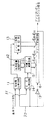
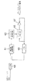
図7は、本発明に係るディジタルPLL回路の第2の実施の形態のブロック構成図である。この実施の形態では、基準クロック信号入力端子と周波数比較回路51の入力側との間に1/Mデバイダ58が挿入接続され、ディジタルPLL回路出力クロック信号出力端子と位相比較回路54ならびに周波数比較回路51の入力側との間に1/Nデバイダ59が挿入接続されたものである。第2の実施の形態にかかるディジタルPLL回路を構成する他の回路要素については上述した第1の実施の形態のディジタルPLL回路の構成と全く同じであるので、その説明は省略する。
【0043】
第1の実施の形態と同様な動作が行われている間、基準クロック信号の周波数のN/M倍の周波数のディジタルPLL回路出力クロック信号を得ることができる。例えば、ディバイダ58が1/4ディバイダであり、ディバイダ59が1/2ディバイダ(すなわち、M=4,N=2)であり、基準クロック信号の周波数が8kHzであった場合、第2の実施の形態にかかるディジタルPLL回路は4kHzの周波数を持つ出力パルスを発生する。
【0044】
図8は、本発明に係るディジタルPLL回路の第3の実施の形態のブロック構成図である。図5の第2の実施の形態のディジタルPLL回路の構成から、位相比較回路及び加算/減算回路を除去した構成となっている。なお、この第3の実施の形態のディジタルPLL回路の構成におけるディレイ制御回路63は、好ましくは負荷容量制御回路及びディレイ段数制御回路(図1および図5)を含むものである。この第3の実施の形態のディジタルPLL回路の構成においては、ディジタルPLL回路出力クロック信号は基準クロック信号の周波数のN/M倍の周波数であるが、両クロック信号の位相は合わされていない。したがって、この実施の形態のPLL回路は、特に位相を合わせる必要のない回路用途、例えば、高周波帯域で動作するLSIの内部クロック等に好適な構成である。
【0045】
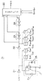
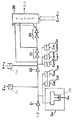
図9は本発明の第4の実施の形態のブロック構成図である。この実施の形態では、加算/減算回路15は位相補正回路115で置き換えられ、負荷容量制御回路12により出力された負荷容量制御情報直接ディレイ可変回路116に与えられている。より詳しくは、位相補正回路115は位相比較回路14の出力を受け取り、補足的負荷容量制御情報を含む出力信号を発生する。ディレイ可変回路116は負荷容量制御回路12、ディレイ段数制御回路13、および位相補正回路115の各出力を受け取って、ディレイ段数制御回路13の出力に基づいてディレイ段数を制御し、負荷容量制御回路12および位相補正回路115の出力に基づいて負荷容量を制御する。
【0046】
図10は図9に示されたディレイ可変回路の好ましい例を示すブロック構成図である。図10のディレイ可変回路116は、2つの付加的な可変負荷容量回路C01およびC02が第1段のインバータ21および22の負荷容量を補足的負荷容量制御信号E01、E02(図9参照)に基づいて設定するために設けられている点を除き、図2のディレイ可変回路と同じである。上述したように、位相補正回路115から位相比較器14の出力に基づいて補足的負荷容量制御信号が出力される。これによりインバータ21および22の負荷容量は負荷容量制御信号Enと補足的負荷容量制御信号E0に基づいて増減される。
【0047】
図9および図10のディジタルPLL回路の出力クロック信号を基準クロック信号に一致させようとする動作は上述した第1の実施の形態の場合と同じである。しかし、出力クロック信号を基準クロック信号に位相を合わせようとするディジタルPLLの動作は次の通りである。位相合わせ動作は位相比較回路14と位相補正回路115(図9)により行われる。上述したように、位相比較回路14は出力クロック信号の位相を基準クロック信号の位相と比較し、位相比較情報を出力する。もし、出力クロック信号の位相が基準クロック信号の位相とが一致したときには、位相補正回路115は「0」および「1」の値を持つ補足的負荷容量制御信号E01、E02をディレイ可変回路116に対して出力する。その結果、付加的可変負荷容量回路C01およびC02のうちの一つがディレイ可変回路における第1段のインバータに接続される。
【0048】
もし、出力クロック信号の位相が基準クロック信号の位相よりも遅れているときは、位相比較器はUP’出力信号を位相補正回路115に与え、双方とも「0」の値を持つ補足的負荷容量制御信号E01、E02をディレイ可変回路116に対して出力させる。この結果、付加的可変負荷容量回路C01およびC02はディレイ可変回路における第1段のインバータに全く接続されず、出力クロック信号の位相は基準クロック信号の位相に対してわずかに進む方向に変位される。
【0049】
逆に、出力クロック信号の位相が基準クロック信号の位相よりも進んでいるときは、位相比較器はDOWN’出力信号を位相補正回路115に与え、双方とも「1」の値を持つ補足的負荷容量制御信号E01、E02をディレイ可変回路116に対して出力させる。この結果、付加的可変負荷容量回路C01およびC02はディレイ可変回路における第1段のインバータに双方とも接続され、出力クロック信号の位相は基準クロック信号の位相に対してわずかに遅れる方向に変位される。このように、位相比較器はディレイ可変回路中で2つの容量を接続したり、切り離したりするのみである。
【0050】
以上のように、本発明の第4の実施の形態は、周波数と位相に関して基準クロック信号と一致したディジタルPLL回路出力信号を提供する。さらに、位相補正回路は第1の実施の形態における加算/減算回路よりも簡単な構成であり、第4の実施の形態は小型でより単純である。
【0051】
図11および図12は本発明のディレイ可変回路のさらに別の例を示すブロック図である。これらの例は可変負荷容量回路の異なる構造を提供する。他の回路要素に関しては図10において説明したのと同じであるので、その説明は省略する。図11の例では、各可変負荷容量回路(例えばCn1)はソースとドレインがインバータ21の出力に共通に接続されたMOSトランジスタ140により構成される。トランジスタ140のゲートは制御信号En1を受ける。このような構成では、トランジスタ140は容量がアナログスイッチと合体されものとして機能する。より詳細には、制御信号が「1」の値を有し、トランジスタのドレインとソースの電位がVDD−Vthよりも低い、すなわち対応するインバータの出力が「0」である場合には、MOSトランジスタのゲート下にはチャネルが形成される。したがってソース、ドレイン間の容量は増加し、インバータの出力が「1」に変化したとき、ディレイを生ずる。他方、制御信号が「0」を持つとき、トランジスタのゲート下にチャネルが形成されず、インバータのディレイは増加しない。
【0052】
図12の例では、各可変負荷容量回路(例えばCn1)はゲートがインバータ21の出力側に接続されたMOSトランジスタ142により形成される。トランジスタ142のソースとドレインは反転制御信号/En1を受けるべく共通接続される。
【0053】
このような構成では、トランジスタ142は反転制御信号/En1が「0」の値を持つとき、容量として機能する。特に、反転制御信号/En1が「0」の値を持ち、トランジスタのゲート電位がVthよりも高い、すなわち、対応するインバータは「1」である場合にはMOSトランジスタのゲート下にはチャネルが形成される。したがって、トランジスタは容量として機能し、インバータの出力を遅延させる。逆に、反転制御信号/En1が「1」の値を持つとき、トランジスタは容量としては機能しない。
【0054】
図11および図12のディレイ可変回路は図10のディレイ可変回路と同様に動作する。しかし、図10の例では各可変負荷容量回路は少なくとも3つのトランジスタを必要とする。これに対し、図11および図12の例では各可変負荷容量回路はトランジスタ1つですむ。したがって、ディレイ可変回路の大きさと複雑さを減少させることができる。さらに、図11の例ではインバータの出力はMOSトランジスタのソース、ドレインと接続されているため、トランジスタのドレイン領域とウェル領域、あるいはソース領域とウェル領域の間で寄生トランジスタが生ずる。例えば、NチャネルMOSトランジスタの場合、寄生容量はN+ドレイン領域とPウェル領域との間で生ずる。このような寄生容量は、インバータの出力に影響を与える。これに対し、図12の例ではMOSトランジスタのゲートに直接接続されているので、寄生容量はインバータ出力に影響を与えない。このように、図12の例は、インバータの出力速度が速いので、高速ディレイ可変回路を実現できる。
【0055】
上述した実施の形態では、ディレイ制御回路は周波数比較回路の出力をもとに制御していたが、本発明はこのような場合に限られない。記載された実施の形態は当業者により周波数比較回路と位相比較回路により制御されるものに適用できる。このような形態では、周波数比較回路および位相比較回路をともに制御させることにより接続段数やディレイ可変回路の出力負荷容量を変化させることになる。
【0056】
【発明の効果】
以上詳細に説明したように、本発明に係るディジタルPLL回路によれば、ディレイ制御回路を周波数比較出力情報に基づき制御することとしたので、複雑な制御用アルゴリズムが不要で設計及び制御が容易な、ジッタの小さい高精度のディジタルPLL回路を構成することができる。
【0057】
さらに、本発明では、ディレイ可変回路が接続段数の変更に無関係な第1および第2のインバータを備えており、2つのインバータよりなるインバータ群が接続段数の変化に影響され、可変負荷容量回路は第1及び第2のインバータの出力に接続され、独立に接続/開放されるようにしているので、ディレイ可変回路により発生するディレイ値は正確に調整することができる。さらに、すべての容量が接続されたときの負荷容量回路で発生したディレイ値は2つのインバータにより発生したディレイ値よりも大きいか等しいので、正確で連続的なディレイ値をディレイ発生回路から得ることができる。
【図面の簡単な説明】
【図1】本発明に係るディジタルPLL回路の第1の実施の形態のブロック構成図。
【図2】図1のディレイ可変回路のブロック構成図。
【図3】ディレイ可変回路のインバータの接続段数とインバータに接続される出力負荷容量とを変更したときのディレイ値の変化を示すグラフ。
【図4】周波数比較回路のブロック構成図。
【図5】位相比較回路のブロック構成図。
【図6】負荷容量制御回路およびディレイ段制御回路のブロック構成図。
【図7】本発明に係るディジタルPLL回路の第2の実施の形態のブロック構成図。
【図8】本発明に係るディジタルPLL回路の第3の実施の形態のブロック構成図。
【図9】本発明に係るディジタルPLL回路の第4の実施の形態のブロック構成図。
【図10】図9のディレイ可変回路の例を示すブロック構成図。
【図11】ディレイ可変回路の他の例を示すブロック構成図。
【図12】ディレイ可変回路の他の例を示すブロック構成図。
【図13】図5の位相比較回路の動作を説明するタイミングチャート。
【図14】従来のディジタルPLL回路のブロック構成図。
【符号の説明】
11、51、61 周波数比較回路
12、52 負荷容量制御回路
13、53、63、73 ディレイ段数制御回路
14、54、74 位相比較回路
15、55 加算/減算回路
16、56、66、76 ディレイ可変回路
17、57、67、77 インバータ
20 マルチプレクサ
21、22 インバータ
23、24 2段インバータ
25 キャパシタ
41、42 10ビットカウンタ
43 10ビットコンパレータ
58、59、68、69 デバイダ
81、88 アップダウンカウンタ
101,102 フリップフロップ
110 位相差検出器
115 位相補正回路
120,130 RSフリップフロップ
Cn1〜Cnm、Cnm+1〜Cnn 負荷容量可変回路[0001]
BACKGROUND OF THE INVENTION
The present invention relates to a digital PLL circuit, and more particularly to a digital PLL circuit having a frequency comparison circuit so that low jitter and high accuracy can be provided without requiring a complicated control algorithm.
[0002]
[Prior art]
Phase-locked loop (PLL) circuits are used in a wide range of fields and can be used in any field suitable for integration. In particular, the PLL circuit is used in various signal circuits such as a frequency synthesizer and a multiplex / stereo demodulation circuit, such as AM / FM radio, television, and wireless communication.
[0003]
In general, the PLL circuit is a feedback loop in which the frequency and phase generated by the variable oscillator are locked to those of the reference signal. The PLL circuit is used to demodulate a baseband signal from a frequency-modulated carrier wave. The basic PLL circuit includes a phase comparison circuit and a voltage controlled oscillator. In operation, the modulated input signal and the output of the voltage controlled oscillator are compared by a phase comparison circuit, and the frequency of the voltage controlled oscillator is controlled by the output of the phase comparison circuit.
FIG. 14 is a block diagram of a conventional digital PLL circuit. As shown in the figure, the reference clock signal is input to the
[0004]
The output signal of the ring oscillator (that is, the output signal of the inverter) is used as an output clock signal, and is input to the
[0005]
Typically, the
[0006]
[Problems to be solved by the invention]
However, in the above-described conventional digital PLL circuit, the
[0007]
For example, even when the frequency of the output clock signal matches the frequency of the reference clock signal, when the phase of the output clock signal is delayed from the phase of the reference clock signal, the delay control circuit is based on the output of the
[0008]
As described above, it is difficult to design a conventional digital PLL circuit, particularly a delay control circuit that can match the phase and frequency of the output clock signal and the reference clock signal. As a result, the conventional design includes a complicated configuration and a very complicated control algorithm for controlling the delay control circuit. In addition, the conventional digital PLL circuit has a slight phase shift even after the PLL circuit has locked once, and the delay control circuit operates to change the delay value of the delay variable circuit. There is also a problem that the jitter of the signal is increased by changing the frequency.
[0009]
The present invention has been made in view of the above problems, and an object of the present invention is to provide a high-precision digital PLL circuit with small jitter that does not require a complicated control algorithm and is easy to design and control.
[0010]
[Means for Solving the Problems]
According to the first aspect of the digital PLL circuit of the present invention,
A frequency comparison circuit that compares the frequency of the output clock signal with the frequency of the reference clock signal and generates frequency comparison information;
A phase comparison circuit that compares the phase of the output clock signal with the phase of the reference clock signal and generates phase comparison information;
A delay control circuit for generating a delay variable digital signal based on the frequency comparison information for the frequency of the output clock signal and the phase comparison information for the phase of the output clock signal;
A variable frequency oscillator that generates an output clock signal that is locked to the frequency and phase of the reference clock signal by the output of the delay control circuit;
With
The delay change amount based on the phase comparison information is characterized in that the unit delay amount is increased or decreased with respect to the delay control information determined by the frequency comparison information.
[0011]
According to the second aspect of the digital PLL circuit of the present invention,
A first frequency divider that divides the output clock signal and generates a divided output clock signal;
A second frequency divider that divides the reference clock signal and generates a divided reference clock signal;
A frequency comparison circuit that compares the frequency of the divided output clock signal with the frequency of the divided reference clock signal and generates frequency comparison information;
A phase comparison circuit that compares the phase of the divided output clock signal with the phase of the divided reference clock signal and generates phase comparison information;
A delay control circuit for generating a delay variable digital signal based on the frequency comparison information for the frequency of the output clock signal and the phase comparison information for the phase of the output clock signal;
A variable frequency oscillator for generating the output clock signal;
The frequency and phase of the output clock signal are controlled based on the frequency comparison information and the phase comparison information, and the variable frequency oscillator uses the output clock signal as N / M times the frequency of the reference clock signal (where M is The frequency division ratio with respect to the reference clock signal in the second frequency divider circuit, and N is the frequency division ratio with respect to the output signal of the delay variable circuit in the first frequency divider circuit, both of which are phase-locked to a natural number) frequency. Output,
The delay change amount based on the phase comparison information is characterized in that the unit delay amount is increased or decreased with respect to the delay control information determined by the frequency comparison information.
[0012]
According to the third aspect of the digital PLL circuit of the present invention,
A comparison means for comparing the reference clock and the output clock;
A load capacity control circuit for generating load capacity control information based on the comparison information from the comparison means;
A delay variable circuit having a variable delay value based on load capacity control information from the load capacity control circuit, and a clock signal generation circuit for outputting a desired output clock signal,
The delay variable circuit includes a load capacitance variable circuit in which the load capacitance control information from the load capacitance control circuit is connected to the source or drain of a MOS transistor, and the gate of the MOS transistor is connected to the delay variable circuit once. Features.
[0014]
DETAILED DESCRIPTION OF THE INVENTION
Hereinafter, some embodiments of a PLL according to the present invention will be described with reference to the drawings.
FIG. 1 is a block configuration diagram of a first embodiment of a digital PLL circuit according to the present invention. The
[0015]
Further, the
[0016]
The addition /
[0017]
Thus, in the present invention, the delay stage number control of the
[0018]
FIG. 2 is a block diagram showing a preferred embodiment of the variable delay circuit shown in FIG. The
[0019]
The operation of the variable delay circuit shown in FIG. 2 will be described. The
[0020]
In order to further control the delay value with high accuracy, as described above, the load capacity variable circuit including the capacitors serving as the output load capacity of each inverter on the output side of the
[0021]
That is, when the values of the load capacity control signals En1 to Enm and Enm + 1 to Enn are “1”, the corresponding analog switch of the load capacity variable circuit to which the signal is input is connected, and the outputs of the
[0022]
FIG. 3 is a graph showing a change in the delay value when the number of inverters connected to the delay variable circuit and the output load capacity connected to the inverter are changed. In the graph, lines OP2, OP4, and OP6 are delay values of the output signal of the delay variable circuit when the number of inverter stages is 2, 4, and 6, respectively. Each graph shows a monotonically increasing (strictly speaking, small step-like) graph, with high delay values due to multiple load capacitance variable circuits arranged on the output side of the two inverters regardless of the change in the number of connection stages. This is due to accuracy control. Furthermore, the delay value control by changing the number of inverter connection stages is control for every two inverter stages, and the amount of delay value adjustment by a plurality of load capacity variable circuits is typically a delay value for two inverter stages. More than the amount. For example, the right end of the graph OP2 and the left end of the graph OP4, and the right end of the graph OP4 and the left end of the graph OP6 are such that the delay values are continuous or partially overlap each other. As described above, the delay variable circuit according to the first embodiment of the present invention can control the delay value continuously with high accuracy.
The operation of the entire digital PLL circuit shown in FIGS. 1 and 2 will be described below. First, the operation of the digital PLL for matching the frequencies of the output clock signal and the reference clock signal will be described.
FIG. 4 is a block diagram of an example of the
[0023]
In response to the frequency comparison information, the load
[0024]
More specifically, when the frequency comparison circuit indicates that the frequency of the output clock signal is higher than the frequency of the reference clock signal, the load
[0025]
If the frequency of the digital PLL circuit output clock signal is higher than the frequency of the reference clock signal even after all of the load capacitance control output signals E′n1 to E′nn are “1”, the load capacitance control is performed at the subsequent frequency comparison. All the output signals E′n1 to E′nn are reset to “0”, and at the same time, this reset information is output to the delay stage
[0026]
The delay stage
[0027]
As described above, according to the first embodiment of the present invention, the frequency of the digital PLL circuit output clock signal is set to the frequency of the reference clock signal by sequentially increasing the number of inverter connection stages and the output load capacity of the inverter. Gradually decreases until In this way, a stable frequency match is established.
[0028]
When the frequency of the digital PLL circuit output clock signal is higher than the frequency of the reference clock signal, the above operation is performed. When the frequency of the digital PLL circuit output clock signal is lower than the frequency of the reference clock signal, the above operation is performed. Performs the reverse operation. That is, based on the frequency comparison output information, when the frequency of the digital PLL circuit output clock signal is lower than the frequency of the reference clock signal, the load
[0029]
If the frequency of the digital PLL circuit output clock signal is lower than the frequency of the reference clock signal even after all of the load capacitance control output signals E′n1 to E′nn have become “0”, the load capacitance control output signal E′n1 ... To Enn are all reset to “1”, and this reset information is output to the delay stage
[0030]
The delay stage
[0031]
As described above, the frequency of the digital PLL circuit output clock signal gradually increases until the frequency becomes the same as the frequency of the reference clock signal by sequentially decreasing the number of inverters connected and the output load capacity of the inverter. In this way, a stable coincidence of frequencies is established.
[0032]
Further, the oscillation frequency of the ring oscillator composed of the
[0033]
Next, the operation (phase matching) for matching the phases of the output clock signal and the reference clock signal of the digital PLL circuit of FIGS. 1 and 2 will be described. Phase matching is performed by the
[0034]
The output of the phase
[0035]
The UP output signal of the phase
[0036]
As described above, the
[0037]
Conversely, if the phase of the digital PLL circuit output clock signal is advanced relative to the phase of the reference clock signal as a result of comparing the phase of the digital PLL circuit output clock signal with the phase of the reference clock signal, the
[0038]
The addition /
[0039]
When the phase of the digital PLL circuit output clock signal matches the phase of the reference clock signal, the addition / subtraction operation of the addition /
[0040]
In the digital PLL circuit according to the present invention, after the frequency comparison is performed, the frequency of the output clock signal is slightly changed during phase matching. More specifically, when addition or subtraction of “1” is performed based on the load capacity control information, the frequency of the output clock signal slightly changes from the frequency set by the frequency matching operation. The next frequency comparison will be affected by the phase matching operation. However, since the frequency comparison is performed once every 1024 clock cycles (in the case of a 10-bit counter), the phase comparison is performed every clock cycle. Therefore, any variation due to the phase matching operation in the load capacity control information is not affected by the phase comparison circuit. And is corrected by an addition / subtraction circuit. Further, since the phase comparison circuit changes the load capacity control information determined by the frequency comparison operation (described above) by “1”, the frequency slightly varies during the phase alignment operation.
[0041]
As described above, in the first embodiment of the present invention, it is possible to obtain a digital PLL circuit output clock signal whose frequency and phase coincide with the reference clock signal. That is, according to the digital PLL circuit of the present invention, it is possible to realize a high-precision digital PLL circuit with small jitter that does not require a complicated control algorithm and is easy to design and control.
[0042]
FIG. 7 is a block diagram of a second embodiment of the digital PLL circuit according to the present invention. In this embodiment, a 1 /
[0043]
While the same operation as that in the first embodiment is performed, a digital PLL circuit output clock signal having a frequency N / M times the frequency of the reference clock signal can be obtained. For example, when the
[0044]
FIG. 8 is a block diagram of a third embodiment of the digital PLL circuit according to the present invention. In this configuration, the phase comparison circuit and the addition / subtraction circuit are removed from the configuration of the digital PLL circuit according to the second embodiment shown in FIG. The
[0045]
FIG. 9 is a block diagram of the fourth embodiment of the present invention. In this embodiment, the addition /
[0046]
FIG. 10 is a block diagram showing a preferred example of the delay variable circuit shown in FIG. In the delay
[0047]
The operation of trying to make the output clock signal of the digital PLL circuit of FIGS. 9 and 10 coincide with the reference clock signal is the same as in the first embodiment described above. However, the operation of the digital PLL that attempts to match the phase of the output clock signal with the reference clock signal is as follows. The phase matching operation is performed by the
[0048]
If the phase of the output clock signal is behind the phase of the reference clock signal, the phase comparator provides the UP 'output signal to the
[0049]
Conversely, when the phase of the output clock signal is ahead of the phase of the reference clock signal, the phase comparator provides the DOWN ′ output signal to the
[0050]
As described above, the fourth embodiment of the present invention provides a digital PLL circuit output signal that matches the reference clock signal with respect to frequency and phase. Furthermore, the phase correction circuit has a simpler configuration than the addition / subtraction circuit in the first embodiment, and the fourth embodiment is small and simpler.
[0051]
11 and 12 are block diagrams showing still another example of the variable delay circuit of the present invention. These examples provide different structures for variable load capacitance circuits. The other circuit elements are the same as those described with reference to FIG. In the example of FIG. 11, each variable load capacitance circuit (for example, Cn1) is configured by a MOS transistor 140 whose source and drain are commonly connected to the output of the
[0052]
In the example of FIG. 12, each variable load capacitance circuit (for example, Cn1) is formed by a
[0053]
In such a configuration, the
[0054]
The variable delay circuit in FIGS. 11 and 12 operates in the same manner as the variable delay circuit in FIG. However, in the example of FIG. 10, each variable load capacitance circuit requires at least three transistors. On the other hand, in the examples of FIGS. 11 and 12, each variable load capacitance circuit requires only one transistor. Therefore, the size and complexity of the variable delay circuit can be reduced. Further, in the example of FIG. 11, since the output of the inverter is connected to the source and drain of the MOS transistor, a parasitic transistor is generated between the drain region and the well region of the transistor or between the source region and the well region. For example, in the case of an N channel MOS transistor, the parasitic capacitance is generated between the N + drain region and the P well region. Such parasitic capacitance affects the output of the inverter. On the other hand, in the example of FIG. 12, since it is directly connected to the gate of the MOS transistor, the parasitic capacitance does not affect the inverter output. Thus, in the example of FIG. 12, since the output speed of the inverter is high, a high-speed delay variable circuit can be realized.
[0055]
In the embodiment described above, the delay control circuit is controlled based on the output of the frequency comparison circuit, but the present invention is not limited to such a case. The described embodiments can be applied to those controlled by a person skilled in the art by means of a frequency comparison circuit and a phase comparison circuit. In such a form, the number of connection stages and the output load capacity of the delay variable circuit are changed by controlling both the frequency comparison circuit and the phase comparison circuit.
[0056]
【The invention's effect】
As described above in detail, according to the digital PLL circuit of the present invention, since the delay control circuit is controlled based on the frequency comparison output information, a complicated control algorithm is not required and design and control are easy. Thus, a highly accurate digital PLL circuit with small jitter can be configured.
[0057]
Furthermore, in the present invention, the delay variable circuit includes the first and second inverters that are irrelevant to the change in the number of connection stages, the inverter group including two inverters is affected by the change in the number of connection stages, and the variable load capacity circuit is Since it is connected to the outputs of the first and second inverters and independently connected / opened, the delay value generated by the variable delay circuit can be adjusted accurately. Further, since the delay value generated in the load capacitance circuit when all the capacitors are connected is greater than or equal to the delay value generated by the two inverters, an accurate and continuous delay value can be obtained from the delay generation circuit. it can.
[Brief description of the drawings]
FIG. 1 is a block configuration diagram of a digital PLL circuit according to a first embodiment of the present invention.
FIG. 2 is a block configuration diagram of the variable delay circuit in FIG. 1;
FIG. 3 is a graph showing changes in the delay value when the number of inverters connected to the variable delay circuit and the output load capacity connected to the inverter are changed.
FIG. 4 is a block configuration diagram of a frequency comparison circuit.
FIG. 5 is a block diagram of a phase comparison circuit.
FIG. 6 is a block configuration diagram of a load capacity control circuit and a delay stage control circuit.
FIG. 7 is a block configuration diagram of a second embodiment of a digital PLL circuit according to the present invention.
FIG. 8 is a block diagram of a digital PLL circuit according to a third embodiment of the present invention.
FIG. 9 is a block diagram of a digital PLL circuit according to a fourth embodiment of the present invention.
10 is a block configuration diagram showing an example of a variable delay circuit in FIG. 9;
FIG. 11 is a block diagram showing another example of the variable delay circuit.
FIG. 12 is a block configuration diagram showing another example of a delay variable circuit.
13 is a timing chart for explaining the operation of the phase comparison circuit of FIG. 5;
FIG. 14 is a block diagram of a conventional digital PLL circuit.
[Explanation of symbols]
11, 51, 61 Frequency comparison circuit
12, 52 Load capacity control circuit
13, 53, 63, 73 Delay stage number control circuit
14, 54, 74 Phase comparison circuit
15, 55 Addition / subtraction circuit
16, 56, 66, 76 Variable delay circuit
17, 57, 67, 77 Inverter
20 Multiplexer
21, 22 Inverter
23, 24 2-stage inverter
25 capacitors
41, 42 10-bit counter
43 10-bit comparator
58, 59, 68, 69 Divider
81, 88 up / down counter
101,102 flip-flop
110 Phase detector
115 Phase correction circuit
120, 130 RS flip-flop
Cn1 to Cnm, Cnm + 1 to Cnn Load capacitance variable circuit
Claims (24)
前記出力クロック信号の位相と前記基準クロック信号の位相とを比較し、位相比較情報を発生する位相比較回路と、
前記出力クロック信号の周波数についての前記周波数比較情報と、前記出力クロック信号の位相についての前記位相比較情報に基づいて、ディレイ可変用ディジタル信号を発生するディレイ制御回路と、
前記ディレイ制御回路の出力により前記基準クロック信号の周波数および位相にロックされるような出力クロック信号を発生する可変周波数発振器と、
を備え
前記位相比較情報によるディレイ変化量は、前記周波数比較情報により決定したディレイ制御情報に対して単位ディレイ量を増加もしくは減少させるものであることを特徴とするディジタルPLL回路。A frequency comparison circuit that compares the frequency of the output clock signal with the frequency of the reference clock signal and generates frequency comparison information;
A phase comparison circuit that compares the phase of the output clock signal with the phase of the reference clock signal and generates phase comparison information;
A delay control circuit for generating a delay variable digital signal based on the frequency comparison information for the frequency of the output clock signal and the phase comparison information for the phase of the output clock signal;
A variable frequency oscillator that generates an output clock signal that is locked to the frequency and phase of the reference clock signal by the output of the delay control circuit;
And a delay variation amount based on the phase comparison information increases or decreases a unit delay amount with respect to delay control information determined by the frequency comparison information.
前記ディレイ制御回路は
前記周波数比較回路からの周波数比較情報と前記位相比較回路からの位相比較情報に基づいて、ディレイ量に対応する負荷容量を制御する制御情報を発生する負荷容量制御回路を備えたことを特徴とする請求項1に記載のディジタルPLL回路。The variable frequency oscillator includes a load capacitance circuit,
The delay control circuit includes a load capacitance control circuit that generates control information for controlling a load capacitance corresponding to a delay amount based on frequency comparison information from the frequency comparison circuit and phase comparison information from the phase comparison circuit. The digital PLL circuit according to claim 1.
前記ディレイ制御回路は
前記周波数比較回路により発生された周波数比較情報に基づいてディレイ段数制御情報を発生するディレイ段数制御回路を備えたことを特徴とする請求項1に記載のディジタルPLL回路。The variable frequency oscillator includes a delay stage number variable circuit,
2. The digital PLL circuit according to claim 1, wherein the delay control circuit includes a delay stage number control circuit that generates delay stage number control information based on the frequency comparison information generated by the frequency comparison circuit.
前記ディレイ制御回路は
前記周波数比較回路からの周波数比較情報および前記位相比較回路からの位相比較情報に基づいてディレイ量に対応する負荷容量制御情報を発生する負荷容量制御回路をさらに備えたことを特徴とする請求項3に記載のディジタルPLL回路。The variable frequency oscillator further comprises a load capacitance circuit,
The delay control circuit further includes a load capacity control circuit that generates load capacity control information corresponding to a delay amount based on frequency comparison information from the frequency comparison circuit and phase comparison information from the phase comparison circuit. The digital PLL circuit according to claim 3.
基準クロック信号を分周し、分周基準クロック信号を発生する第2の分周回路と、
前記分周出力クロック信号の周波数と前記分周基準クロック信号の周波数とを比較し、周波数比較情報を発生する周波数比較回路と、
前記分周出力クロック信号の位相と前記分周基準クロック信号の位相とを比較し、位相比較情報を発生する位相比較回路と、
前記出力クロック信号の周波数についての前記周波数比較情報と、前記出力クロック信号の位相についての前記位相比較情報に基づいて、ディレイ可変用ディジタル信号を発生するディレイ制御回路と、
前記出力クロック信号を発生する可変周波数発振器を備え、
前記出力クロック信号の周波数および位相の制御は前記周波数比較情報と前記位相比較情報に基づいて行われ、前記可変周波数発振器は出力クロック信号を基準クロック信号の周波数のN/M倍(ただし、Mは前記第2の分周回路における基準クロック信号に対する周波数分割比、Nは前記第1の分周回路におけるディレイ可変回路の出力信号に対する周波数分割比であって、いずれも自然数)の周波数に位相ロックして出力し、
前記位相比較情報によるディレイ変化量は、前記周波数比較情報により決定したディレイ制御情報に対して単位ディレイ量を増加もしくは減少させるものであることを特徴とするディジタルPLL回路。A first frequency divider that divides the output clock signal and generates a divided output clock signal;
A second frequency divider that divides the reference clock signal and generates a divided reference clock signal;
A frequency comparison circuit that compares the frequency of the divided output clock signal with the frequency of the divided reference clock signal and generates frequency comparison information;
A phase comparison circuit that compares the phase of the divided output clock signal with the phase of the divided reference clock signal and generates phase comparison information;
A delay control circuit for generating a delay variable digital signal based on the frequency comparison information for the frequency of the output clock signal and the phase comparison information for the phase of the output clock signal;
A variable frequency oscillator for generating the output clock signal;
The frequency and phase of the output clock signal are controlled based on the frequency comparison information and the phase comparison information, and the variable frequency oscillator uses the output clock signal as N / M times the frequency of the reference clock signal (where M is The frequency division ratio with respect to the reference clock signal in the second frequency divider circuit and N is the frequency division ratio with respect to the output signal of the delay variable circuit in the first frequency divider circuit, both of which are phase-locked to a natural number) frequency. Output,
The digital PLL circuit according to claim 1, wherein the delay change amount based on the phase comparison information increases or decreases a unit delay amount with respect to delay control information determined by the frequency comparison information.
前記ディレイ制御回路は
前記周波数比較回路からの周波数比較情報と位相比較回路からの位相比較情報に基づいて、ディレイ量に対応する負荷容量制御情報を発生する負荷容量制御回路を備えたことを特徴とする請求項12に記載のディジタルPLL回路。The variable frequency oscillator includes a variable load capacitance circuit,
The delay control circuit includes a load capacity control circuit that generates load capacity control information corresponding to a delay amount based on frequency comparison information from the frequency comparison circuit and phase comparison information from the phase comparison circuit. The digital PLL circuit according to claim 12.
前記ディレイ制御回路は
前記周波数比較回路により発生された周波数比較情報に基づいてディレイ段制御情報を発生するディレイ段数制御回路を備えたことを特徴とする請求項12に記載のディジタルPLL回路。The variable frequency oscillator includes a delay stage number variable circuit,
13. The digital PLL circuit according to claim 12, wherein the delay control circuit includes a delay stage number control circuit that generates delay stage control information based on frequency comparison information generated by the frequency comparison circuit.
前記ディレイ制御回路は
前記周波数比較情報および前記位相比較情報に基づいて負荷容量制御情報を発生する負荷容量制御回路をさらに備えたことを特徴とする請求項14に記載のディジタルPLL回路。The variable frequency oscillator further comprises a load capacitance circuit,
15. The digital PLL circuit according to claim 14, wherein the delay control circuit further comprises a load capacitance control circuit that generates load capacitance control information based on the frequency comparison information and the phase comparison information.
前記比較手段からの比較情報をもとに負荷容量制御情報を発生させる負荷容量制御回路と、
前記負荷容量制御回路からの負荷容量制御情報をもとにディレイ値可変なディレイ可変回路を含み、所望の出力クロック信号を出力するクロック信号発生回路とを備え、
前記ディレイ可変回路は前記負荷容量制御回路からの負荷容量制御情報をMOSトランジスタのソースもしくはドレインに接続し、前記MOSトランジスタのゲートを前記ディレイ可変回路の一端に接続した負荷容量可変回路を有することを特徴とするディジタルPLL回路。A comparison means for comparing the reference clock and the output clock;
A load capacity control circuit for generating load capacity control information based on the comparison information from the comparison means;
A delay variable circuit having a variable delay value based on load capacity control information from the load capacity control circuit, and a clock signal generation circuit for outputting a desired output clock signal,
The variable delay circuit includes a variable load capacitance circuit in which load capacitance control information from the load capacitance control circuit is connected to a source or drain of a MOS transistor, and a gate of the MOS transistor is connected to one end of the delay variable circuit. A featured digital PLL circuit.
Priority Applications (3)
| Application Number | Priority Date | Filing Date | Title |
|---|---|---|---|
| US08/772,008 US5923715A (en) | 1996-12-19 | 1996-12-19 | Digital phase-locked loop circuit |
| KR1019960072717A KR100245579B1 (en) | 1995-12-28 | 1996-12-27 | Digital pll circuit |
| JP35106296A JP3607026B2 (en) | 1995-12-28 | 1996-12-27 | Digital PLL circuit |
Applications Claiming Priority (4)
| Application Number | Priority Date | Filing Date | Title |
|---|---|---|---|
| JP34316795 | 1995-12-28 | ||
| JP7-343167 | 1995-12-28 | ||
| US08/772,008 US5923715A (en) | 1996-12-19 | 1996-12-19 | Digital phase-locked loop circuit |
| JP35106296A JP3607026B2 (en) | 1995-12-28 | 1996-12-27 | Digital PLL circuit |
Publications (2)
| Publication Number | Publication Date |
|---|---|
| JPH09238072A JPH09238072A (en) | 1997-09-09 |
| JP3607026B2 true JP3607026B2 (en) | 2005-01-05 |
Family
ID=27341079
Family Applications (1)
| Application Number | Title | Priority Date | Filing Date |
|---|---|---|---|
| JP35106296A Expired - Fee Related JP3607026B2 (en) | 1995-12-28 | 1996-12-27 | Digital PLL circuit |
Country Status (2)
| Country | Link |
|---|---|
| JP (1) | JP3607026B2 (en) |
| KR (1) | KR100245579B1 (en) |
Families Citing this family (4)
| Publication number | Priority date | Publication date | Assignee | Title |
|---|---|---|---|---|
| JP3540589B2 (en) | 1998-02-02 | 2004-07-07 | 株式会社東芝 | Clock multiplication circuit |
| WO2004079913A1 (en) * | 2003-03-06 | 2004-09-16 | Fujitsu Limited | Digital pll circuit |
| DE102004006996B4 (en) * | 2004-02-12 | 2006-09-28 | Infineon Technologies Ag | Digital phase locked loop with fast transient response |
| JP5198166B2 (en) | 2008-06-27 | 2013-05-15 | 富士通セミコンダクター株式会社 | Digital DLL circuit and semiconductor device |
-
1996
- 1996-12-27 KR KR1019960072717A patent/KR100245579B1/en not_active Expired - Fee Related
- 1996-12-27 JP JP35106296A patent/JP3607026B2/en not_active Expired - Fee Related
Also Published As
| Publication number | Publication date |
|---|---|
| KR970055560A (en) | 1997-07-31 |
| KR100245579B1 (en) | 2000-02-15 |
| JPH09238072A (en) | 1997-09-09 |
Similar Documents
| Publication | Publication Date | Title |
|---|---|---|
| US5923715A (en) | Digital phase-locked loop circuit | |
| US6252465B1 (en) | Data phase locked loop circuit | |
| US5629651A (en) | Phase lock loop having a reduced synchronization transfer period | |
| JP3415304B2 (en) | Clock generation circuit and processor | |
| US6870411B2 (en) | Phase synchronizing circuit | |
| KR101190313B1 (en) | A Self noise Suppressing Voltage Controlled Oscillator | |
| KR101252048B1 (en) | A Frequency-Phase-Locked Loop with a Self-Noise Suppressing Voltage Controlled Oscillator | |
| US8125253B2 (en) | System and method for dynamically switching between low and high frequency reference clock to PLL and minimizing PLL output frequency changes | |
| US6859079B2 (en) | Semiconductor device capable of accurately producing internal multi-phase clock signal | |
| KR20190139007A (en) | Assymetric pulse width comparator circuit and clock phase correction circuit including the same | |
| US7292079B2 (en) | DLL-based programmable clock generator using a threshold-trigger delay element circuit and a circular edge combiner | |
| US5081428A (en) | Voltage controlled oscillator having 50% duty cycle clock | |
| JP3313631B2 (en) | Integrated circuit | |
| US7268635B2 (en) | Circuits for voltage-controlled ring oscillators and method of generating a periodic signal | |
| JP2008135835A (en) | PLL circuit | |
| JP3607026B2 (en) | Digital PLL circuit | |
| CN114301452B (en) | Phase-locked loop circuit, control method, charge pump and chip | |
| US7385432B2 (en) | Commutating phase selector | |
| US7301413B2 (en) | Voltage controlled oscillator and PLL circuit | |
| CN116488620A (en) | Duty cycle correction circuit and chip | |
| JP7514162B2 (en) | PLL circuit using intermittent amplifier | |
| JPH07326964A (en) | Digital phase lock loop | |
| CN116488619A (en) | Duty cycle correction circuit and chip | |
| JP2004120215A (en) | Voltage controlled oscillator, PLL frequency synthesizer, and integrated circuit | |
| WO2008018276A1 (en) | Voltage controlled oscillator, frequency synthesizer and oscillating frequency control method |
Legal Events
| Date | Code | Title | Description |
|---|---|---|---|
| A521 | Written amendment |
Free format text: JAPANESE INTERMEDIATE CODE: A523 Effective date: 20040831 |
|
| A61 | First payment of annual fees (during grant procedure) |
Free format text: JAPANESE INTERMEDIATE CODE: A61 Effective date: 20041006 |
|
| FPAY | Renewal fee payment (event date is renewal date of database) |
Free format text: PAYMENT UNTIL: 20081015 Year of fee payment: 4 |
|
| FPAY | Renewal fee payment (event date is renewal date of database) |
Free format text: PAYMENT UNTIL: 20081015 Year of fee payment: 4 |
|
| FPAY | Renewal fee payment (event date is renewal date of database) |
Free format text: PAYMENT UNTIL: 20091015 Year of fee payment: 5 |
|
| FPAY | Renewal fee payment (event date is renewal date of database) |
Free format text: PAYMENT UNTIL: 20101015 Year of fee payment: 6 |
|
| FPAY | Renewal fee payment (event date is renewal date of database) |
Free format text: PAYMENT UNTIL: 20111015 Year of fee payment: 7 |
|
| FPAY | Renewal fee payment (event date is renewal date of database) |
Free format text: PAYMENT UNTIL: 20111015 Year of fee payment: 7 |
|
| FPAY | Renewal fee payment (event date is renewal date of database) |
Free format text: PAYMENT UNTIL: 20121015 Year of fee payment: 8 |
|
| LAPS | Cancellation because of no payment of annual fees |