JP3604635B2 - Electric circuit having circuit component and method of testing circuit component - Google Patents
Electric circuit having circuit component and method of testing circuit component Download PDFInfo
- Publication number
- JP3604635B2 JP3604635B2 JP2001017347A JP2001017347A JP3604635B2 JP 3604635 B2 JP3604635 B2 JP 3604635B2 JP 2001017347 A JP2001017347 A JP 2001017347A JP 2001017347 A JP2001017347 A JP 2001017347A JP 3604635 B2 JP3604635 B2 JP 3604635B2
- Authority
- JP
- Japan
- Prior art keywords
- bus
- circuit
- output
- test
- data
- Prior art date
- Legal status (The legal status is an assumption and is not a legal conclusion. Google has not performed a legal analysis and makes no representation as to the accuracy of the status listed.)
- Expired - Fee Related
Links
Images

Classifications
-
- G—PHYSICS
- G01—MEASURING; TESTING
- G01R—MEASURING ELECTRIC VARIABLES; MEASURING MAGNETIC VARIABLES
- G01R31/00—Arrangements for testing electric properties; Arrangements for locating electric faults; Arrangements for electrical testing characterised by what is being tested not provided for elsewhere
- G01R31/26—Testing of individual semiconductor devices
-
- G—PHYSICS
- G01—MEASURING; TESTING
- G01R—MEASURING ELECTRIC VARIABLES; MEASURING MAGNETIC VARIABLES
- G01R31/00—Arrangements for testing electric properties; Arrangements for locating electric faults; Arrangements for electrical testing characterised by what is being tested not provided for elsewhere
- G01R31/28—Testing of electronic circuits, e.g. by signal tracer
- G01R31/317—Testing of digital circuits
- G01R31/3181—Functional testing
- G01R31/3185—Reconfiguring for testing, e.g. LSSD, partitioning
- G01R31/318505—Test of Modular systems, e.g. Wafers, MCM's
-
- H—ELECTRICITY
- H10—SEMICONDUCTOR DEVICES; ELECTRIC SOLID-STATE DEVICES NOT OTHERWISE PROVIDED FOR
- H10P—GENERIC PROCESSES OR APPARATUS FOR THE MANUFACTURE OR TREATMENT OF DEVICES COVERED BY CLASS H10
- H10P74/00—Testing or measuring during manufacture or treatment of wafers, substrates or devices
Landscapes
- Physics & Mathematics (AREA)
- General Physics & Mathematics (AREA)
- Engineering & Computer Science (AREA)
- General Engineering & Computer Science (AREA)
- Tests Of Electronic Circuits (AREA)
- Test And Diagnosis Of Digital Computers (AREA)
Description
【0001】
【発明の属する技術分野】
本発明は、バスを介して接続された回路コンポーネントを有する電気回路に関する。本発明はまた、バスを介して接続された複数の回路コンポーネントのうち1つの回路コンポーネントをテストする方法に関する。
【0002】
【従来の技術】
テストすべき回路コンポーネントは例えば集積回路のいわゆるマクロである。集積回路をテストする際には所定のマクロを個々に、すなわち集積回路の他の回路コンポーネントから独立にテストしなければならない。
【0003】
この種のテストでは集積回路の比較的小さい部分のみがテストされるが、この種のテストは特にテスト中この集積回路を通って流れるきわめて高い電流とこれに関連した極端な温度上昇とのためにしばしば大きなコストがかかる。さらに前述の理由から実際の状態に相応しないテスト結果が得られることもある。
【0004】
【発明が解決しようとする課題】
本発明の課題は、テストすべき回路コンポーネントを最小のコストで確実にテストできるようにすることである。
【0005】
【課題を解決するための手段】
この課題は、少なくとも1つの回路コンポーネントは他の回路コンポーネントとは独立にテスト可能であり、他の回路コンポーネントとは独立にテスト可能な少なくとも1つの回路コンポーネントは当該の回路コンポーネントの通常動作中にもテスト中にもデータを形成し、このデータはバスへ出力することもできるし、また回路コンポーネントのテストのために設けられたテストユニットへバスを介さずに供給することもでき、当該の回路コンポーネントの通常動作中はデータはバスへ出力され、当該の回路コンポーネントのテスト中はデータはバスへは出力されない構成の電気回路により解決される。
【0006】
課題はまた、少なくとも1つの回路コンポーネントを他の回路コンポーネントとは独立にテスト可能であり、テストされる回路コンポーネントは通常動作中にもテスト中にもデータを形成し、このデータはバスへ出力することもできるし、また当該の回路コンポーネントのテストのために設けられたテストユニットへバスを介さずに供給することもでき、当該の回路コンポーネントの通常動作中はデータをバスへ出力し、当該の回路コンポーネントのテスト中はデータをバスへは出力しないことにより解決される。
【0007】
【発明の実施の形態】
本発明の特徴により、テストすべき回路コンポーネントの出力ドライバがエネルギを全く消費しないか、またはきわめて僅かしか消費しない状態が達成される。このことはテストすべき回路コンポーネントを介してデータがバスへ出力されないケースで明らかであるが、データがバスへ出力されるケースでも相当する。すなわちテストすべき回路コンポーネントのテスト中にバスへ出力されるデータは当該の回路コンポーネントが通常動作中にバスへ出力するデータと同一ではなく、出力ドライバのエネルギ消費が最小となるように選定されて出力されるのである。
【0008】
出力ドライバは、バスへ出力されるデータが変更されないか、またはきわめてまれにしか変更されない場合、特に僅かなエネルギ消費しか有さない。ここで相当の容量を有するバス線路のローディング切換は特にクロック周波数が高い場合には比較的大きな電流を必要とするが、本発明ではこのローディング切換(アップロード/ダウンロード切換)を全く行わなくてよくなるか、またはほとんど行わなくてよくなる。このようにバス線路のローディングが全くまたはほとんど必要ないことは、出力ドライバからの大きな電流の送出が全く必要ないかほとんど必要なくなるので有利である。さらにこれにより当該の回路コンポーネントはテストの際に必要な処置を採用しなかった場合と比べて格段に小さな温度上昇で済む。
【0009】
出力ドライバの小さな電流消費、ひいてはこれに結びついた利点は、付加的または選択的にバスへ出力すべきデータのタスクをテスト中は出力ドライバを回避して行うことにより達成される。出力ドライバはテスト中遮断されるか、または不活性化される。
【0010】
テストすべき回路コンポーネントは、テスト中、通常であれば出力されるデータをバスへ出力しないか、および/または通常のデータと異なるデータを出力するが、テスト結果には影響はない。テストすべき回路コンポーネントは別の回路コンポーネントとは独立にテストされるので、これによりバスを介して回路コンポーネントと電気回路との間のデータ交換を行う必要はない。
【0011】
独立請求項記載の特徴を有する電気回路およびテスト方法によれば、テストすべき回路コンポーネントを最小コストで確実にテストすることができる。
【0012】
本発明の有利な実施形態は、従属請求項、以下の説明および図から得られる。
【0013】
【実施例】
本発明を以下に実施例に則して図に関連して詳細に説明する。
【0014】
以下に説明する電気回路は集積回路である。しかしこれは何ら限定されるものでないことを指摘しておく。この電気回路は任意の別の電気回路であってよい。
【0015】
この電気回路の第1の実施例は図1に示されている。
【0016】
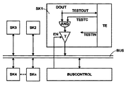
図1に示された電気回路は回路コンポーネント(マクロ)SK1,SK2,...,SKn、これらの回路コンポーネントSK1,SK2,...,SKnに接続されたバスBUS、およびバスBUSの制御(特にアービトレーション)を担当するバス制御装置BUSCONTROLから成る。
【0017】
回路コンポーネントSK1,SK2,...,SKnのなかに、個々に、すなわち他の回路コンポーネントとは独立に、電気回路によってテストされる少なくとも1つの回路コンポーネントが存在する。これは、この実施例では、SK1で示された回路コンポーネントである。
【0018】
回路コンポーネントSK1はこの実施例ではメモリモジュールであり、より正確に言えばDRAMマクロである。ただしこれも何ら限定されるものではないことを指摘しておく。以下に説明するテスト可能な回路コンポーネントは任意の回路部分であってよい。
【0019】
回路コンポーネントSK1をテストするためにテストユニットTEが設けられている。このテストユニットはこの実施例ではテストすべき回路コンポーネントSK1の構成部分である。ただしこれも限定されるものではない。テストユニットTEをテストすべき回路コンポーネントSK1の外部に設けることもできる。この場合、ユニットを電気回路内部の任意の位置に配置してもよいし、その外部に配置してもよい。
【0020】
テストユニットTEはa)テストデータTESTINをテストすべき回路コンポーネントSK1へ入力結合し、b)テストデータTESTOUTをテストすべき回路コンポーネントSK1から出力し、c)テストすべき回路コンポーネントSK1をテスト制御信号TESTCにより制御し、d)テストデータTESTIN、TESTOUTに基づいてテストすべき回路コンポーネントSK1が正しく動作しているか否かを検査する。
【0021】
回路コンポーネントSK1の通常動作時、すなわち回路コンポーネントSK1がテストされていない場合には、a)回路コンポーネントSK1にバスBUSと図1には示されていないデータ受信装置とを介してデータが供給され、b)回路コンポーネントSK1により複数の出力ドライバ(このうち図1には唯一の出力ドライバTのみが示されている)を介してデータがバスBUSへ出力される。
【0022】
出力ドライバTはこの実施例ではいわゆるトライステートドライバであり、バス制御装置BUSCONTROLによって制御される。より正確に言えば出力ドライバは出力されたイネーブル信号ENによって活性化ないし不活性化される。出力ドライバTが活性化されている場合、すなわちこの実施例のEN=1である場合、出力ドライバは個々に供給されるデータをバスBUSへ出力する。出力ドライバTが不活性状態である場合、すなわちこの実施例のEN=0である場合、データはバスBUSへは出力されない。出力ドライバはその場合高オーム状態にある。
【0023】
回路コンポーネントSK1のテスト中には、a)回路コンポーネントSK1によりバスBUSを介して供給されるデータの代わりにテストユニットTEのテストデータTESTINが使用され、b)このデータがテストユニットTEのテストデータTESTOUTとして使用される。つまりc)通常動作でバスBUSへ出力されるデータに代えて、別のデータがバスへ出力される。
【0024】
回路コンポーネントSK1のテスト中にバスBUSへ出力されるデータは、この実施例では、本来バスへ出力すべきデータとは無関係に形成される。このデータは全く変更されないか、またはきわめてまれにしか変更されないという特殊性を有する。
【0025】
この実施例では、回路コンポーネントSK1のテスト中、持続的にレベル“0”を表すデータをバスBUSへ出力する。
【0026】
いつどんなデータがバスBUSへ出力されるかは、この実施例では出力ドライバTの前方に接続された論理素子により定められる。
【0027】
論理素子はこの実施例ではAND素子ANDから成り、回路コンポーネントSK1の通常動作中にバスBUSへ出力すべきデータDOUTおよびテスト制御信号TESTCを入力信号として受け取る。論理素子の出力信号は出力ドライバTに入力信号として供給される。
【0028】
テスト制御信号TESTCは回路コンポーネントSK1の通常動作中は値“1”を有する。これによりAND素子の出力信号DOUTはAND素子の入力信号に相応する。これにより回路コンポーネントSK1の通常動作中は本来バスBUSへ出力すべきデータDOUTがバスへ出力される。
【0029】
回路コンポーネントSK1のテスト中、テスト制御信号は値“0”を有する。これによりAND素子の出力信号はAND素子の他の入力信号の値には無関係に値“0”を取る。これにより回路コンポーネントSK1のテスト中は持続的に値“0”がバスへ出力される。
【0030】
回路コンポーネントSK1のテスト中には全く変更されないかまたはほとんど変更されないデータがバスBUSへ出力されることにより、バス線路がローディング切換を全く行わなくてよいか、またはほとんど行わなくてよいという有利な効果が得られる。これはa)出力ドライバTが僅かなエネルギしか消費せず、b)出力ドライバTおよび回路コンポーネントSK1が過剰に加熱されないので有利である。
【0031】
電気回路がテスト中わずかなエネルギしか消費せず、これにより電気回路のテスト中比較的低い温度が維持されることにより、テストすべき回路コンポーネントSK1を最小のコストで確実にテストできる。これは特にa)電気回路にテスト中エネルギを供給する部材(ニードル)の数およびサイズを小さく維持でき、b)比較的簡単に低温テストを行えることにより達成される。
【0032】
回路コンポーネントSK1のテスト中には本来バスBUSへ出力すべきデータDOUTでなく別のデータがバスへ出力されるが、負の影響がテスト結果に作用することはない。テストすべき回路コンポーネントSK1は他の回路コンポーネントから独立して電気回路によってテストされるので、回路コンポーネントSK1からバスへデータが出力されるか否か、または出力されるデータがどんなものであるかということは重要な意味を持たない。
【0033】
回路コンポーネントSK1がデータをバスBUSへ出力しない構成は有利であると判明している。仮に回路コンポーネントSK1が出力ドライバをテスト中自動的に不活性化する(すなわち高オーム状態へ移行させる)ように構成したとすると、問題が発生する可能性がある。一般にはバスBUSに接続されている全てのコンポーネントは短時間であっても同時に高オーム状態へ移行する出力ドライバを有してはならないからである。バスBUSはつねに接続されているコンポーネントによって終端していなければならない。
【0034】
ただし本発明によればこの問題は発生しない。このためバス制御装置は回路コンポーネントSK1のテスト中変更されずに更に処理され、唯一の制御はバスBUSを介して行われる。更にこれにより複数の回路コンポーネントを電気回路によって同時にテスト可能となる。
【0035】
回路コンポーネントSK1のテスト中必ずしも持続的にレベル“0”を表すデータをバスBUSへ出力しなくともよいことがわかる。ここでは持続的にレベル“1”を表すデータをバスBUSへ出力することもできる。さらに回路コンポーネントSK1のテスト中、持続的に所定のレベルを有するデータをバスBUSへ出力するのではなく、バスへ出力されるデータを変更することもできる。ただしバスへ出力されるデータはまれにしか変更できない。このようにして不変のデータをバスへ出力する場合とほぼ同じ有利な効果を達成することができる。
【0036】
同様に、バスへ出力すべきデータを形成する論理素子が必ずしも前述のように構成ないし配置されたAND素子でなくともよい。これに対しては多数の他の手段が考えられる。例えばAND素子に代えてNAND素子を使用してもよいし、また選択的に通常動作で出力すべきデータDOUTまたはテスト中の出力データを出力ドライバTへ導通するマルチプレクサを使用してもよい。
【0037】
電気回路はテストすべき回路コンポーネントがテスト中にデータをバスへ出力しないように構成することもできる。
【0038】
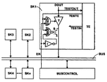
この種の電気回路の実施例を図2に示し、以下にこれを参照しながら説明する。
【0039】
図2に示されている電気回路は図1に示された電気回路に完全に相応する。図2に示された電気回路は図1に示された電気回路と同様に、回路コンポーネント(マクロ)SK1,SK2,...,SKn、これらの回路コンポーネントSK1,SK2,...,SKnに接続されたバスBUS、およびこのバスBUSの制御(特にアービトレーション)を担当するバス制御装置BUSCONTROLから成る。またここに存在している回路コンポーネントSK1,SK2,...,SKnのなかに、個々にすなわち他の回路コンポーネントから独立して電気回路によってテストされる参照番号SK1で示された回路コンポーネントが存在する。テストすべき回路コンポーネントのテストは図1の電気回路内に設けられているテストユニットTEと同様に、テストすべき回路コンポーネントすなわち回路コンポーネントSK1内に含まれているテストユニットTEによって行われる。ここまでは図1の電気回路と図2の電気回路とは一致している。
【0040】
図1の回路コンポーネントSK1とは異なって、図2の回路コンポーネントSK1はテスト中にバスBUSへデータを出力しない。
【0041】
この実施例では、図2の回路コンポーネントSK1に設けられている出力ドライバTの(制御)端子にはバス制御装置BUSCONTROLから出力されるイネーブル信号ENではなく、制御端子に前置接続されている論理素子の出力信号が印加される。出力ドライバは制御端子を介して活性化ないし不活性化される。
【0042】
この論理素子はこの実施例ではAND素子ANDから成っており、この論理素子はイネーブル信号ENおよび図2の電気回路に設けられているテスト制御信号TESTCを入力信号として受け取る。論理素子の出力信号は出力ドライバTの制御に使用される。
【0043】
テスト制御信号TESTCは回路コンポーネントSK1の通常動作中に値“1”を有する。これにより回路コンポーネントSK1の通常動作中、出力ドライバの制御に使用されるこの信号はイネーブル信号ENに相応する。
【0044】
回路コンポーネントSK1のテスト中、テスト制御信号TESTCは値“0”を有する。したがって回路コンポーネントSK1のテスト中、出力ドライバTの制御に使用される信号は持続的に値“0”を有する。これにより出力ドライバTは不活性化され、データはバスBUSへ出力されない。
【0045】
図1の電気回路とは異なり、図2の電気回路ではテスト制御信号TESTCはテストすべき回路コンポーネントSK1のみにではなく、バスターミネーション論理素子BTLにも供給される。この論理素子はこの実施例ではバス制御装置BUSCONTROLの構成部分である。
【0046】
バスターミネーション論理素子BTLは、バスBUSが回路コンポーネントSK1のテスト中(テスト制御信号TESTCによって回路コンポーネントSK1のテストが信号化されている間)バスBUSに接続された他のコンポーネントによって終端されるように制御する。この実施例では、バスターミネーション論理素子BTLはバスBUSを必要に応じてそれ自体で終端させる。これに代えてバスターミネーション論理素子BTLが回路コンポーネントSK1のテスト中に、バスBUSに接続された他の1つの回路コンポーネントの出力ドライバを活性化し、当該のコンポーネントをバスに終端させるように構成してもよい。
【0047】
論理素子を使用して出力ドライバTを制御する制御信号が形成されるが、これは必ずしも前述のように構成ないし配置されたAND素子でなくともよい。このために多数の別の手段がある。すなわち例えばAND素子に代えてNAND素子を使用してもよいし、また選択的にイネーブル信号ENまたは出力ドライバTの制御端子を制御するテスト制御信号TESTCを導通するマルチプレクサを使用してもよい。
【0048】
回路コンポーネントSK1のテスト中データがバスBUSへ出力されないことにより、出力ドライバTがエネルギを全く消費しないか、または無視できる程度に小さいエネルギ消費しか有さず、これにより温度上昇は全く生じないか、きわめて僅かしか生じないという有利な作用が得られる。
【0049】
電気回路がテスト中僅かしかエネルギを消費せず、したがってこの電気回路はテスト中比較的低温に維持されることにより、テストすべき回路コンポーネントSK1は最小のコストで確実にテストされる。これは特にa)電気回路にテスト中エネルギを供給する部材(ニードル)の数およびサイズが小さく維持され、b)比較的簡単に低温テストが実行できることにより達成される。
【0050】
これらの利点は図2の電気回路で図1の電気回路よりもさらに際立っている。
【0051】
図3に示された参照番号にしたがって以下に説明する電気回路によれば、図1の電気回路の利点、すなわちテストすべき回路コンポーネントのテスト中、場合により必要なバスのターミネーションがテストすべき回路コンポーネント自体により行われる利点と、図2の電気回路の利点、すなわちテストすべき回路コンポーネントの出力ドライバがテスト中全くエネルギを消費しないか、または無視できる程度に小さなエネルギしか消費しない利点とが同時に得られる。
【0052】
図3に示された電気回路はその大部分が図1、図2に示された電気回路に相応する。図3に示された電気回路は図1、図2に示された電気回路と同様に回路コンポーネント(マクロ)SK1,SK2,...,SKn、これらの回路コンポーネントSK1,SK2,...,SKnに接続されたバスBUS、およびバスBUSの制御(特にアービトレーション)を担当するバス制御装置BUSCONTROLから成る。またここに存在している回路コンポーネントSK1,SK2,...,SKnのなかに、個々にすなわち他の回路コンポーネントから独立して電気回路によってテストされる参照番号SK1で示された回路コンポーネントが存在する。テストすべき回路コンポーネントのテストは図1、図2の電気回路内に設けられているテストユニットTEと同様にテストすべき回路コンポーネントすなわち回路コンポーネントSK1内に含まれているテストユニットTEによって行われる。ここまでの点では図1、図2の電気回路と図3の電気回路とは一致している。
【0053】
図1の回路コンポーネントSK1と同様に、ただし図2の回路コンポーネントSK1とは異なって、図3の回路コンポーネントSK1はテスト中必要に応じて(特に回路コンポーネントSK1がバス制御装置BUSCONTROLによりバスパターンとして定められている場合に)データをバスBUSへ出力する。
【0054】
このことはこの実施例では、図3の回路コンポーネントSK1に設けられている出力ドライバTを介してではなく、出力ドライバTの出力端子とバスBUSとの間に存在する位置に所定の電位または所定の電圧特性を印加することにより行われる。
【0055】
ここでの所定の電位はこの実施例ではアース電位である。ただしこれは任意の他の電位であってもよいし、また時間的に変化する電位であってもよい。
【0056】
出力ドライバTの出力端子とバスBUSとの間に存在する位置への所定の電位または所定の電圧特性の印加は、この実施例ではスイッチング装置Sを介して行われ、このスイッチング装置はここではトランジスタによって形成される。この場合基本的にトランジスタの形態は重要な意味を有さない。トランジスタに代えて任意の他のスイッチング装置、例えばいわゆるトランスミッションゲートを使用することもできる。
【0057】
スイッチング装置Sは論理素子により制御される。論理素子はこの実施例ではNOR素子NORおよびインバータIから成っており、NOR素子はテスト制御信号TESTCを入力信号として受け取り、インバータIは反転されたイネーブル信号ENを入力信号として受け取る。NOR素子の出力信号はスイッチング装置Sを制御するために使用される。
【0058】
テスト制御信号TESTCおよびイネーブル信号ENは図1、図2の電気回路での同名の信号に相応する。
【0059】
テストすべき回路コンポーネントSK1の出力ドライバTはテスト中は不活性化されている。不活性化はこの実施例では、出力ドライバTを活性化ないし不活性化するこのドライバの制御端子に対して、図2の電気回路での場合と同様に、この制御端子に前置接続された論理素子の出力信号が印加されることにより達成される。
【0060】
論理素子はこの実施例では図2の電気回路での場合と同様にAND素子から成っており、テスト制御信号TESTCおよびイネーブル信号ENを入力信号として受け取る。この論理素子の出力信号は出力ドライバTを制御するために使用される。
【0061】
バスBUSのターミネーションを制御するスイッチング装置Sと出力ドライバTとは論理素子AND、I、NORによって制御され、その結果次の関係が得られる。
【0062】
【表1】

図3の電気回路はa)図1の電気回路に比べて、通常動作でデータDOUTが出力される経路に付加的な論理素子が存在せず、これによりデータ出力を迅速に行うことができ、また出力ドライバがテストすべき回路コンポーネントのテスト中に不活性化されているので、テスト中に僅かなエネルギしか消費せず、したがって僅かしか温度が上昇しない利点を有しており、b)図2の電気回路に比べて、テストすべき回路コンポーネント自体がバスを終端するため、バスターミネーション論理素子BTLまたは同様の装置を省略できる利点を有する。またこの電気回路によって図1、図2の電気回路に比べて重大な欠点を甘受しなければならないということもない。
【0064】
出力ドライバTおよびスイッチング装置Sを制御する制御信号の形成に使用される論理素子は必ずしも前述のように構成ないし配置しなくてもよい。これに対して多数の別の手段が可能である。
【0065】
出力ドライバTが回路コンポーネントSK1のテスト中不活性化されていることにより、このドライバはエネルギを全く消費しないか、または無視できる程度に小さいエネルギしか消費しないので有利である。したがって温度上昇も全く生じないか、またはほとんど生じない。
【0066】
電気回路がテスト中僅かしかエネルギを消費せず、したがってこの電気回路はテスト中比較的低温に維持されることにより、テストすべき回路コンポーネントSK1は最小のコストで確実にテストされる。これは特にa)電気回路にテスト中エネルギを供給する部材(ニードル)の数およびサイズが小さく維持され、b)比較的簡単に低温テストが実行できることにより達成される。
【0067】
テストすべき回路コンポーネントをテストするための当該の手段は通常動作中にも格別の影響を有さない。特にテストすべき回路コンポーネントの動作速度や他の主要な特性に対して影響を与えるおそれは全くない。
【0068】
前述の電気回路は実際の実現形態での個々の独立性とは無関係に驚くほど簡単に構成できる。これによりテストすべき回路コンポーネントを最小のコストで確実にテストすることができる。
【図面の簡単な説明】
【図1】電気回路の第1の実施例を説明するための図である。
【図2】電気回路の第2の実施例を説明するための図である。
【図3】電気回路の第3の実施例を説明するための図である。
【符号の説明】
SK1,SK2,...,SKn 回路コンポーネント
BUS バス
BUSCONTROL バス制御装置
T 出力ドライバ
TE テストユニット
AND AND素子
NOR NOR素子
I インバータ
S スイッチング装置
TESTIN,TESTOUT テストデータ
TESTTC テスト制御信号
EN イネーブル信号
DOUT 出力データ[0001]
TECHNICAL FIELD OF THE INVENTION
The present invention relates to an electric circuit having circuit components connected via a bus. The present invention also relates to a method of testing one of a plurality of circuit components connected via a bus.
[0002]
[Prior art]
The circuit component to be tested is, for example, a so-called macro of an integrated circuit. In testing integrated circuits, certain macros must be tested individually, i.e., independently of other circuit components of the integrated circuit.
[0003]
Although such tests test only a relatively small portion of the integrated circuit, such tests are particularly difficult due to the extremely high current flowing through the integrated circuit during testing and the associated extreme temperature rise. Often costs a lot. Furthermore, test results that do not correspond to actual conditions may be obtained for the reasons described above.
[0004]
[Problems to be solved by the invention]
It is an object of the present invention to ensure that the circuit components to be tested can be tested with minimum cost.
[0005]
[Means for Solving the Problems]
The problem is that at least one circuit component can be tested independently of the other circuit components, and at least one circuit component that can be tested independently of the other circuit components can be tested during normal operation of the circuit component. During the test, data can be formed and this data can be output to the bus or can be supplied to the test unit provided for testing the circuit component without passing through the bus, During normal operation, data is output to the bus, and during testing of the circuit component in question, data is not output to the bus.
[0006]
The problem is also that at least one circuit component can be tested independently of other circuit components, wherein the circuit component to be tested forms data both during normal operation and during testing, and this data is output on the bus. It can also be supplied to a test unit provided for testing the circuit component without a bus, and outputs data to the bus during normal operation of the circuit component, and The solution is to not output data to the bus during testing of the circuit components.
[0007]
BEST MODE FOR CARRYING OUT THE INVENTION
According to a feature of the invention, a situation is achieved in which the output driver of the circuit component to be tested consumes no or very little energy. This is apparent in the case where data is not output to the bus via the circuit component to be tested, but also in the case where data is output to the bus. That is, the data output to the bus during the test of the circuit component to be tested is not the same as the data output by the circuit component to the bus during normal operation, and is selected so that the energy consumption of the output driver is minimized. It is output.
[0008]
The output driver has a particularly low energy consumption if the data output on the bus is unchanged or changes very rarely. Here, the loading switching of the bus line having a considerable capacity requires a relatively large current, especially when the clock frequency is high. In the present invention, is it unnecessary to perform this loading switching (upload / download switching) at all? Or hardly ever. This little or no need for bus line loading is advantageous because little or no need to deliver large currents from the output driver. In addition, the circuit component requires a significantly lower temperature rise than if the necessary measures were not taken during the test.
[0009]
The low current consumption of the output driver, and consequently the associated advantages, is achieved by additionally or selectively performing the task of the data to be output onto the bus while avoiding the output driver during testing. The output driver is shut off or deactivated during the test.
[0010]
During the test, the circuit component to be tested does not output data that would normally be output to the bus and / or outputs data different from the normal data, but does not affect the test results. The circuit component to be tested is tested independently of the other circuit components, so that there is no need to exchange data between the circuit components and the electrical circuit via the bus.
[0011]
According to the electric circuit and the test method having the features described in the independent claims, it is possible to reliably test the circuit component to be tested at a minimum cost.
[0012]
Advantageous embodiments of the invention result from the dependent claims, the following description and the figures.
[0013]
【Example】
BRIEF DESCRIPTION OF THE DRAWINGS The invention will be explained in more detail below with reference to an exemplary embodiment and with reference to the drawings.
[0014]
The electric circuit described below is an integrated circuit. However, it should be pointed out that this is not a limitation. This electrical circuit may be any other electrical circuit.
[0015]
A first embodiment of this electric circuit is shown in FIG.
[0016]
The electric circuit shown in FIG. 1 includes circuit components (macro) SK1, SK2,. . . , SKn, these circuit components SK1, SK2,. . . , SKn, and a bus controller BUSCONTROL which controls the bus BUS (especially, arbitration).
[0017]
The circuit components SK1, SK2,. . . , SKn, there is at least one circuit component to be tested individually, ie independently of the other circuit components, by an electric circuit. This is the circuit component designated SK1 in this embodiment.
[0018]
The circuit component SK1 is a memory module in this embodiment, more precisely a DRAM macro. It should be noted, however, that this is not a limitation. The testable circuit components described below may be any circuit part.
[0019]
A test unit TE is provided for testing the circuit component SK1. This test unit is a component of the circuit component SK1 to be tested in this embodiment. However, this is not limited. The test unit TE can also be provided outside the circuit component SK1 to be tested. In this case, the unit may be arranged at an arbitrary position inside the electric circuit or outside the electric circuit.
[0020]
The test unit TE a) couples the test data TESTIN to the circuit component SK1 to be tested, b) outputs the test data TESTOUT from the circuit component SK1 to be tested, and c) transmits the circuit component SK1 to be tested to the test control signal TESTC. And d) checking whether or not the circuit component SK1 to be tested is operating correctly based on the test data TESTIN and TESTOUT.
[0021]
During normal operation of the circuit component SK1, ie, when the circuit component SK1 has not been tested, a) data is supplied to the circuit component SK1 via the bus BUS and a data receiving device not shown in FIG. b) Data is output to the bus BUS by the circuit component SK1 via a plurality of output drivers (of which only one output driver T is shown in FIG. 1).
[0022]
The output driver T is a so-called tri-state driver in this embodiment, and is controlled by a bus controller BUSCONTROL. To be more precise, the output driver is activated or deactivated by the output enable signal EN. When the output driver T is activated, that is, when EN = 1 in this embodiment, the output driver outputs individually supplied data to the bus BUS. When the output driver T is inactive, that is, when EN = 0 in this embodiment, no data is output to the bus BUS. The output driver is then in a high ohmic state.
[0023]
During the test of the circuit component SK1, a) the test data TESTIN of the test unit TE is used instead of the data supplied by the circuit component SK1 via the bus BUS, and b) this data is the test data TESTOUT of the test unit TE. Used as That is, c) another data is output to the bus instead of the data output to the bus BUS in the normal operation.
[0024]
In this embodiment, the data output to the bus BUS during the test of the circuit component SK1 is formed independently of the data to be output to the bus. This data has the peculiarity that it is not changed at all or changes very rarely.
[0025]
In this embodiment, during the test of the circuit component SK1, data representing the level “0” is continuously output to the bus BUS.
[0026]
When and what data is output to the bus BUS is determined by a logic element connected in front of the output driver T in this embodiment.
[0027]
The logic element comprises an AND element AND in this embodiment, and receives as input signals the data DOUT to be output to the bus BUS and the test control signal TESTC during the normal operation of the circuit component SK1. The output signal of the logic element is supplied to the output driver T as an input signal.
[0028]
The test control signal TESTC has the value “1” during the normal operation of the circuit component SK1. Thus, the output signal DOUT of the AND element corresponds to the input signal of the AND element. Thus, during the normal operation of the circuit component SK1, the data DOUT to be output to the bus BUS is output to the bus.
[0029]
During the test of the circuit component SK1, the test control signal has the value "0". As a result, the output signal of the AND element takes the value "0" regardless of the values of other input signals of the AND element. As a result, the value “0” is continuously output to the bus during the test of the circuit component SK1.
[0030]
The advantage that no or little loading switching is required on the bus line by the fact that data that is not changed or hardly changed during the test of the circuit component SK1 is output on the bus BUS. Is obtained. This is advantageous because a) the output driver T consumes little energy and b) the output driver T and the circuit component SK1 are not overheated.
[0031]
Since the electrical circuit consumes little energy during the test and thus maintains a relatively low temperature during the testing of the electrical circuit, the circuit component SK1 to be tested can be reliably tested with minimum cost. This is achieved in particular by a) keeping the number and size of the members (needle) supplying energy to the electrical circuit during the test small, and b) making the low temperature test relatively easy.
[0032]
During the test of the circuit component SK1, other data than the data DOUT to be output to the bus BUS is output to the bus, but no negative influence does not affect the test result. Since the circuit component SK1 to be tested is tested by an electric circuit independently of the other circuit components, it is determined whether or not data is output from the circuit component SK1 to the bus, or what the output data is. That has no significant meaning.
[0033]
An arrangement in which the circuit component SK1 does not output data on the bus BUS has proven to be advantageous. If the circuit component SK1 is configured to automatically deactivate the output driver during the test (that is, shift to the high ohmic state), a problem may occur. Generally, all components connected to the bus BUS must not have an output driver that simultaneously transitions to the high ohm state even for a short time. The bus BUS must be terminated by always connected components.
[0034]
However, according to the present invention, this problem does not occur. For this purpose, the bus controller is further processed without change during the test of the circuit component SK1, the only control taking place via the bus BUS. Furthermore, this allows a plurality of circuit components to be tested simultaneously by an electrical circuit.
[0035]
It can be seen that during the test of the circuit component SK1, data representing the level “0” does not always have to be output to the bus BUS. Here, data representing the level "1" can be continuously output to the bus BUS. Further, during the test of the circuit component SK1, instead of outputting data having a predetermined level to the bus BUS continuously, it is possible to change data output to the bus. However, the data output to the bus can be rarely changed. In this way, almost the same advantageous effects as in the case of outputting unchanged data to the bus can be achieved.
[0036]
Similarly, the logic elements forming the data to be output to the bus need not necessarily be the AND elements configured or arranged as described above. Numerous other means are conceivable for this. For example, a NAND element may be used instead of the AND element, or a multiplexer for selectively conducting data DOUT to be output in normal operation or output data under test to the output driver T may be used.
[0037]
The electrical circuit may be configured such that the circuit component to be tested does not output data to the bus during the test.
[0038]
An embodiment of this type of electric circuit is shown in FIG. 2 and will be described below with reference thereto.
[0039]
The electric circuit shown in FIG. 2 completely corresponds to the electric circuit shown in FIG. The electric circuit shown in FIG. 2 is similar to the electric circuit shown in FIG. 1 and includes circuit components (macros) SK1, SK2,. . . , SKn, these circuit components SK1, SK2,. . . , SKn, and a bus control device BUSCONTROL which controls the bus BUS (especially, arbitration). The circuit components SK1, SK2,. . . , SKn, there is a circuit component indicated by reference number SK1 which is tested by the electric circuit individually, ie independently of the other circuit components. The test of the circuit component to be tested is performed by the test unit TE included in the circuit component to be tested, that is, the circuit component SK1, similarly to the test unit TE provided in the electric circuit of FIG. Up to this point, the electric circuit of FIG. 1 and the electric circuit of FIG. 2 match.
[0040]
Unlike the circuit component SK1 of FIG. 1, the circuit component SK1 of FIG. 2 does not output data to the bus BUS during a test.
[0041]
In this embodiment, the (control) terminal of the output driver T provided in the circuit component SK1 of FIG. 2 is not an enable signal EN output from the bus control device BUSCONTROL, but a logic connected in front of the control terminal. The output signal of the device is applied. The output driver is activated or deactivated via the control terminal.
[0042]
This logic element comprises an AND element AND in this embodiment, which receives as input signals an enable signal EN and a test control signal TESTC provided in the electric circuit of FIG. The output signal of the logic element is used for controlling the output driver T.
[0043]
The test control signal TESTC has the value “1” during the normal operation of the circuit component SK1. Thereby, during normal operation of the circuit component SK1, this signal used for controlling the output driver corresponds to the enable signal EN.
[0044]
During the test of the circuit component SK1, the test control signal TESTC has the value “0”. Thus, during the test of the circuit component SK1, the signal used for controlling the output driver T has the value "0" continuously. As a result, the output driver T is inactivated, and no data is output to the bus BUS.
[0045]
Unlike the electric circuit of FIG. 1, in the electric circuit of FIG. 2, the test control signal TESTC is supplied not only to the circuit component SK1 to be tested but also to the bus termination logic element BTL. This logic element is a component of the bus controller BUSCONTROL in this embodiment.
[0046]
The bus termination logic element BTL is such that the bus BUS is terminated by another component connected to the bus BUS during the test of the circuit component SK1 (while the test of the circuit component SK1 is signaled by the test control signal TESTC). Control. In this embodiment, the bus termination logic BTL terminates the bus BUS itself as needed. Instead, the bus termination logic element BTL activates the output driver of another circuit component connected to the bus BUS during the test of the circuit component SK1, and terminates the component on the bus. Is also good.
[0047]
A control signal for controlling the output driver T is formed using a logic element, but this is not necessarily an AND element configured or arranged as described above. There are a number of alternatives for this. That is, for example, a NAND element may be used in place of the AND element, or a multiplexer that selectively conducts the enable signal EN or the test control signal TESTC for controlling the control terminal of the output driver T may be used.
[0048]
Since no data is output on the bus BUS during the test of the circuit component SK1, the output driver T consumes no energy or has negligible energy consumption, so that no temperature rise occurs, The advantageous effect that very little occurs is obtained.
[0049]
Since the electrical circuit consumes little energy during the test and is therefore kept relatively cool during the test, the circuit component SK1 to be tested is reliably tested at a minimum cost. This is achieved in particular by a) keeping the number and size of the components (needle) supplying energy to the electrical circuit during the test small, and b) making it relatively easy to carry out low temperature tests.
[0050]
These advantages are even more pronounced in the circuit of FIG. 2 than in the circuit of FIG.
[0051]
According to the electrical circuit described below in accordance with the reference numbers shown in FIG. 3, the advantage of the electrical circuit of FIG. The advantages provided by the component itself and the advantages of the electrical circuit of FIG. 2, i.e., that the output driver of the circuit component under test consumes no or negligible energy during the test, are obtained. Can be
[0052]
The electric circuit shown in FIG. 3 largely corresponds to the electric circuit shown in FIGS. The electric circuit shown in FIG. 3 is similar to the electric circuits shown in FIGS. 1 and 2, and has circuit components (macro) SK1, SK2,. . . , SKn, these circuit components SK1, SK2,. . . , SKn, and a bus controller BUSCONTROL which controls the bus BUS (especially, arbitration). The circuit components SK1, SK2,. . . , SKn, there is a circuit component indicated by reference number SK1 which is tested by the electric circuit individually, ie independently of the other circuit components. The test of the circuit component to be tested is carried out by the test unit TE included in the circuit component to be tested, that is, the circuit component SK1, similarly to the test unit TE provided in the electric circuit of FIGS. Up to this point, the electric circuits of FIGS. 1 and 2 and the electric circuit of FIG. 3 match.
[0053]
Like the circuit component SK1 of FIG. 1, but different from the circuit component SK1 of FIG. 2, the circuit component SK1 of FIG. 3 can be used as needed during the test (in particular, the circuit component SK1 is defined as a bus pattern by the bus controller BUSCONTROL). Output data to the bus BUS (if enabled).
[0054]
This means that, in this embodiment, the predetermined potential or the predetermined potential is not set via the output driver T provided in the circuit component SK1 of FIG. 3 but at a position existing between the output terminal of the output driver T and the bus BUS. Is performed by applying the voltage characteristics of
[0055]
The predetermined potential here is a ground potential in this embodiment. However, this may be any other potential or a potential that changes with time.
[0056]
The application of a given potential or a given voltage characteristic to the position present between the output terminal of the output driver T and the bus BUS is effected in this embodiment via a switching device S, which here comprises a transistor Formed by In this case, the configuration of the transistor basically has no significant meaning. Any other switching device can be used in place of the transistor, for example a so-called transmission gate.
[0057]
The switching device S is controlled by a logic element. The logic element in this embodiment comprises a NOR element NOR and an inverter I. The NOR element receives a test control signal TESTC as an input signal, and the inverter I receives an inverted enable signal EN as an input signal. The output signal of the NOR element is used to control the switching device S.
[0058]
The test control signal TESTC and the enable signal EN correspond to the signals of the same names in the electric circuits of FIGS.
[0059]
The output driver T of the circuit component SK1 to be tested is inactive during the test. In this embodiment, the deactivation is preceded by a control terminal of this driver which activates or deactivates the output driver T, as in the case of the electric circuit of FIG. This is achieved by applying the output signal of the logic element.
[0060]
The logic element in this embodiment is composed of an AND element as in the case of the electric circuit of FIG. 2, and receives the test control signal TESTC and the enable signal EN as input signals. The output signal of this logic element is used to control the output driver T.
[0061]
The switching device S for controlling the termination of the bus BUS and the output driver T are controlled by the logic elements AND, I, NOR, so that the following relationship is obtained.
[0062]
[Table 1]
The electric circuit of FIG. 3 a) has no additional logic element in the path where the data DOUT is output in the normal operation as compared with the electric circuit of FIG. 1, whereby the data can be output quickly. It also has the advantage that the output driver is deactivated during the test of the circuit component to be tested, so that it consumes only a small amount of energy during the test and therefore only a small increase in temperature, b) FIG. This has the advantage that the bus termination logic element BTL or similar device can be omitted, since the circuit component to be tested itself terminates the bus. In addition, this electrical circuit does not require any significant disadvantages compared to the electrical circuits of FIGS.
[0064]
The logic elements used to generate the control signals for controlling the output driver T and the switching device S need not necessarily be configured or arranged as described above. A number of alternatives are possible for this.
[0065]
Advantageously, since the output driver T is deactivated during the test of the circuit component SK1, it consumes no energy or consumes negligible energy. Therefore, no or almost no temperature rise occurs.
[0066]
Since the electrical circuit consumes little energy during the test and is therefore kept relatively cool during the test, the circuit component SK1 to be tested is reliably tested at a minimum cost. This is achieved in particular by a) keeping the number and size of the components (needle) supplying energy to the electrical circuit during the test small, and b) making it relatively easy to carry out low temperature tests.
[0067]
Such means for testing the circuit components to be tested have no particular effect during normal operation. In particular, there is no risk of affecting the operating speed or other key characteristics of the circuit component to be tested.
[0068]
The above-mentioned electrical circuits are surprisingly simple to construct independently of the individual independence in the actual implementation. This ensures that the circuit components to be tested can be tested with minimal cost.
[Brief description of the drawings]
FIG. 1 is a diagram for explaining a first embodiment of an electric circuit.
FIG. 2 is a diagram for explaining a second embodiment of the electric circuit.
FIG. 3 is a diagram for explaining a third embodiment of the electric circuit.
[Explanation of symbols]
SK1, SK2,. . . , SKn Circuit component BUS Bus BUS CONTROL Bus controller T Output driver TE Test unit AND AND element NOR NOR element I Inverter S Switching device TESTIN, TESTOUT Test data TESTTC Test control signal EN Enable signal DOUT Output data
Claims (21)
少なくとも1つの回路コンポーネント(SK1)は他の回路コンポーネント(SK2〜SKn)とは独立にテスト可能であり、
他の回路コンポーネント(SK2〜SKn)とは独立にテスト可能な少なくとも1つの回路コンポーネント(SK1)は当該の回路コンポーネントの通常動作中にもテスト中にもデータ(DOUT)を形成し、
該データはバスへ出力することもできるし、また回路コンポーネントのテストのために設けられたテストユニット(TE)へバスを介さずに供給することもでき、
当該の回路コンポーネントの通常動作中はデータはバスへ出力され、
当該の回路コンポーネントのテスト中はデータはバス(BUS)へは出力されない
ことを特徴とする回路コンポーネントを有する電気回路。In an electric circuit having circuit components (SK1 to SKn) connected via a bus (BUS),
At least one circuit component (SK1) is testable independently of the other circuit components (SK2-SKn);
At least one circuit component (SK1), which can be tested independently of the other circuit components (SK2 to SKn), forms data (DOUT) both during normal operation and during testing of the circuit component;
The data can be output to a bus, or can be supplied without a bus to a test unit (TE) provided for testing circuit components,
During normal operation of the circuit component, data is output to the bus,
An electric circuit having a circuit component, wherein data is not output to a bus (BUS) during a test of the circuit component.
少なくとも1つの回路コンポーネント(SK1)を他の回路コンポーネント(SK2〜SKn)とは独立にテスト可能であり、
テストされる回路コンポーネント(SK1)は通常動作中にもテスト中にもデータ(DOUT)を形成し、
該データはバスへ出力することもできるし、また当該の回路コンポーネントのテストのために設けられたテストユニット(TE)へバスを介さずに供給することもでき、
当該の回路コンポーネントの通常動作中はデータをバスへ出力し、
当該の回路コンポーネントのテスト中はデータをバス(BUS)へは出力しない
ことを特徴とする回路コンポーネントをテストする方法。A method for testing one circuit component (SK1) of a plurality of circuit components (SK1 to SKn) connected via a bus (BUS),
At least one circuit component (SK1) can be tested independently of the other circuit components (SK2-SKn);
The circuit component under test (SK1) forms data (DOUT) both during normal operation and during testing,
The data can be output to a bus, or can be supplied to a test unit (TE) provided for testing the circuit component without passing through the bus,
During normal operation of the circuit component, it outputs data to the bus,
A method for testing a circuit component, wherein data is not output to a bus (BUS) during the test of the circuit component.
Applications Claiming Priority (4)
| Application Number | Priority Date | Filing Date | Title |
|---|---|---|---|
| DE10003260.5 | 2000-01-26 | ||
| DE10003260 | 2000-01-26 | ||
| DE10016127A DE10016127A1 (en) | 2000-01-26 | 2000-03-31 | Electrical circuit for testing integrated circuit components especially macro type electronic components, where one or more components can be tested independently of the other components, where data on the bus can be turned off |
| DE10016127.8 | 2000-03-31 |
Publications (2)
| Publication Number | Publication Date |
|---|---|
| JP2001235518A JP2001235518A (en) | 2001-08-31 |
| JP3604635B2 true JP3604635B2 (en) | 2004-12-22 |
Family
ID=26004033
Family Applications (1)
| Application Number | Title | Priority Date | Filing Date |
|---|---|---|---|
| JP2001017347A Expired - Fee Related JP3604635B2 (en) | 2000-01-26 | 2001-01-25 | Electric circuit having circuit component and method of testing circuit component |
Country Status (6)
| Country | Link |
|---|---|
| US (1) | US6701473B2 (en) |
| EP (1) | EP1132750B1 (en) |
| JP (1) | JP3604635B2 (en) |
| KR (1) | KR100437556B1 (en) |
| DE (1) | DE50015199D1 (en) |
| TW (1) | TW503322B (en) |
Families Citing this family (2)
| Publication number | Priority date | Publication date | Assignee | Title |
|---|---|---|---|---|
| US7308439B2 (en) | 2001-06-06 | 2007-12-11 | Hyperthink Llc | Methods and systems for user activated automated searching |
| JP2019045960A (en) * | 2017-08-30 | 2019-03-22 | 株式会社東芝 | Disk unit |
Family Cites Families (11)
| Publication number | Priority date | Publication date | Assignee | Title |
|---|---|---|---|---|
| JP2713724B2 (en) | 1988-04-19 | 1998-02-16 | 株式会社日立製作所 | Semiconductor integrated circuit |
| JP2827229B2 (en) * | 1988-10-14 | 1998-11-25 | 日本電気株式会社 | Semiconductor integrated circuit |
| JPH04138388A (en) | 1990-09-29 | 1992-05-12 | Fuji Electric Co Ltd | Semiconductor integrated circuit and controlling method thereof |
| JP2806075B2 (en) * | 1991-06-06 | 1998-09-30 | 日本電気株式会社 | Microcomputer |
| US5136185A (en) * | 1991-09-20 | 1992-08-04 | Hewlett-Packard Company | Local tristate control circuit |
| JPH0696599A (en) | 1992-02-26 | 1994-04-08 | Nec Corp | Semiconductor integrated circuit |
| DE59410250D1 (en) * | 1993-08-30 | 2003-04-10 | Infineon Technologies Ag | Processor circuit with test facility |
| US6041427A (en) * | 1997-10-27 | 2000-03-21 | Vlsi Technology | Scan testable circuit arrangement |
| JPH11248802A (en) | 1998-03-06 | 1999-09-17 | Sony Corp | Semiconductor device |
| WO1999056396A2 (en) * | 1998-04-23 | 1999-11-04 | Koninklijke Philips Electronics N.V. | Testable ic having analog and digital circuits |
| US6499124B1 (en) * | 1999-05-06 | 2002-12-24 | Xilinx, Inc. | Intest security circuit for boundary-scan architecture |
-
2000
- 2000-12-21 EP EP00128175A patent/EP1132750B1/en not_active Expired - Lifetime
- 2000-12-21 DE DE50015199T patent/DE50015199D1/en not_active Expired - Lifetime
-
2001
- 2001-01-20 TW TW090101508A patent/TW503322B/en not_active IP Right Cessation
- 2001-01-25 JP JP2001017347A patent/JP3604635B2/en not_active Expired - Fee Related
- 2001-01-26 KR KR10-2001-0003725A patent/KR100437556B1/en not_active Expired - Fee Related
- 2001-01-26 US US09/771,391 patent/US6701473B2/en not_active Expired - Lifetime
Also Published As
| Publication number | Publication date |
|---|---|
| TW503322B (en) | 2002-09-21 |
| EP1132750B1 (en) | 2008-06-11 |
| JP2001235518A (en) | 2001-08-31 |
| EP1132750A3 (en) | 2003-07-02 |
| EP1132750A2 (en) | 2001-09-12 |
| KR20010078080A (en) | 2001-08-20 |
| US6701473B2 (en) | 2004-03-02 |
| DE50015199D1 (en) | 2008-07-24 |
| US20020008538A1 (en) | 2002-01-24 |
| KR100437556B1 (en) | 2004-06-26 |
Similar Documents
| Publication | Publication Date | Title |
|---|---|---|
| US7034565B2 (en) | On-die termination circuit and method for reducing on-chip DC current, and memory system including memory device having the same | |
| US7170313B2 (en) | Apparatus for calibrating termination voltage of on-die termination | |
| US6275077B1 (en) | Method and apparatus for programmable adjustment of bus driver propagation times | |
| US7868656B2 (en) | Hot plug control apparatus and method | |
| JP2006516780A (en) | Method and apparatus for controlling a data processing system during debugging | |
| EP1825280A2 (en) | Using parametric measurement units as a source of power for a device under test | |
| JP3604635B2 (en) | Electric circuit having circuit component and method of testing circuit component | |
| JP2008524597A (en) | Circuit and method for detecting voltage in a device under test using a parametric measurement unit | |
| US7057397B1 (en) | Output impedance measurement techniques | |
| US8395406B2 (en) | Integrated circuit architecture for testing variable delay circuit | |
| WO2020217925A1 (en) | Semiconductor integrated circuit device and inspection method for semiconductor integrated circuit device | |
| JPH08507610A (en) | Device for testing connections with pulling resistance | |
| JP2007317345A (en) | Semiconductor integrated circuit device | |
| CN1763555B (en) | Semiconductor integrated circuit | |
| US7285976B2 (en) | Integrated circuit with programmable-impedance output buffer and method therefor | |
| US20050216803A1 (en) | Integrated circuit device | |
| US20240319260A1 (en) | State transition control for parametric measurement unit | |
| KR100321177B1 (en) | Printed circuit board of a memory module | |
| JP2001215463A (en) | LCD driver common output setting circuit and setting method, and semiconductor device for LCD driver | |
| JP2021141204A (en) | Semiconductor integrated circuit device and inspection method for semiconductor integrated circuit device | |
| KR20070017651A (en) | Semiconductor memory device and method having termination resistor on input pin | |
| JPH1152019A (en) | Semiconductor integrated circuit | |
| JPS6129485A (en) | Memory circuit | |
| JP4947689B2 (en) | Semiconductor integrated circuit and test method thereof | |
| JP2003156534A (en) | Semiconductor integrated circuit |
Legal Events
| Date | Code | Title | Description |
|---|---|---|---|
| A131 | Notification of reasons for refusal |
Free format text: JAPANESE INTERMEDIATE CODE: A131 Effective date: 20040220 |
|
| A521 | Request for written amendment filed |
Free format text: JAPANESE INTERMEDIATE CODE: A523 Effective date: 20040518 |
|
| TRDD | Decision of grant or rejection written | ||
| A01 | Written decision to grant a patent or to grant a registration (utility model) |
Free format text: JAPANESE INTERMEDIATE CODE: A01 Effective date: 20040903 |
|
| A61 | First payment of annual fees (during grant procedure) |
Free format text: JAPANESE INTERMEDIATE CODE: A61 Effective date: 20040929 |
|
| R150 | Certificate of patent or registration of utility model |
Free format text: JAPANESE INTERMEDIATE CODE: R150 |
|
| FPAY | Renewal fee payment (event date is renewal date of database) |
Free format text: PAYMENT UNTIL: 20071008 Year of fee payment: 3 |
|
| FPAY | Renewal fee payment (event date is renewal date of database) |
Free format text: PAYMENT UNTIL: 20081008 Year of fee payment: 4 |
|
| FPAY | Renewal fee payment (event date is renewal date of database) |
Free format text: PAYMENT UNTIL: 20091008 Year of fee payment: 5 |
|
| FPAY | Renewal fee payment (event date is renewal date of database) |
Free format text: PAYMENT UNTIL: 20091008 Year of fee payment: 5 |
|
| FPAY | Renewal fee payment (event date is renewal date of database) |
Free format text: PAYMENT UNTIL: 20101008 Year of fee payment: 6 |
|
| FPAY | Renewal fee payment (event date is renewal date of database) |
Free format text: PAYMENT UNTIL: 20101008 Year of fee payment: 6 |
|
| FPAY | Renewal fee payment (event date is renewal date of database) |
Free format text: PAYMENT UNTIL: 20111008 Year of fee payment: 7 |
|
| FPAY | Renewal fee payment (event date is renewal date of database) |
Free format text: PAYMENT UNTIL: 20121008 Year of fee payment: 8 |
|
| FPAY | Renewal fee payment (event date is renewal date of database) |
Free format text: PAYMENT UNTIL: 20121008 Year of fee payment: 8 |
|
| FPAY | Renewal fee payment (event date is renewal date of database) |
Free format text: PAYMENT UNTIL: 20131008 Year of fee payment: 9 |
|
| R250 | Receipt of annual fees |
Free format text: JAPANESE INTERMEDIATE CODE: R250 |
|
| R250 | Receipt of annual fees |
Free format text: JAPANESE INTERMEDIATE CODE: R250 |
|
| R250 | Receipt of annual fees |
Free format text: JAPANESE INTERMEDIATE CODE: R250 |
|
| R250 | Receipt of annual fees |
Free format text: JAPANESE INTERMEDIATE CODE: R250 |
|
| R250 | Receipt of annual fees |
Free format text: JAPANESE INTERMEDIATE CODE: R250 |
|
| LAPS | Cancellation because of no payment of annual fees |