JP3601382B2 - Inspection apparatus and inspection method using charged particle beam - Google Patents

Inspection apparatus and inspection method using charged particle beam Download PDF

Info

Publication number
JP3601382B2
JP3601382B2 JP32644099A JP32644099A JP3601382B2 JP 3601382 B2 JP3601382 B2 JP 3601382B2 JP 32644099 A JP32644099 A JP 32644099A JP 32644099 A JP32644099 A JP 32644099A JP 3601382 B2 JP3601382 B2 JP 3601382B2
Authority
JP
Japan
Prior art keywords
charged particle
particle beam
sample
stage
scanning
Prior art date
Legal status (The legal status is an assumption and is not a legal conclusion. Google has not performed a legal analysis and makes no representation as to the accuracy of the status listed.)
Expired - Fee Related
Application number
JP32644099A
Other languages
Japanese (ja)
Other versions
JP2000215834A (en
Inventor
欣之 七田
康弘 郡司
高志 広井
雅嗣 亀谷
昌宏 小山
健次郎 山本
拓 二宮
Current Assignee (The listed assignees may be inaccurate. Google has not performed a legal analysis and makes no representation or warranty as to the accuracy of the list.)
Hitachi Ltd
Original Assignee
Hitachi Ltd
Priority date (The priority date is an assumption and is not a legal conclusion. Google has not performed a legal analysis and makes no representation as to the accuracy of the date listed.)
Filing date
Publication date
Application filed by Hitachi Ltd filed Critical Hitachi Ltd
Priority to JP32644099A priority Critical patent/JP3601382B2/en
Publication of JP2000215834A publication Critical patent/JP2000215834A/en
Application granted granted Critical
Publication of JP3601382B2 publication Critical patent/JP3601382B2/en
Anticipated expiration legal-status Critical
Expired - Fee Related legal-status Critical Current

Links

Images

Description

【0001】
【発明の属する技術分野】
本発明は、微細な回路パターンを有するメモリ,LSI等の半導体装置や液晶,ホトマスク等の回路パターンの検査装置および検査方法に係わり、特に荷電粒子線を用いた検査装置および検査方法に関する。
【0002】
【従来の技術】
半導体装置は、半導体ウエハ上にホトマスクに形成された回路パターンをリソグラフィー処理およびエッチング処理により転写する工程を繰り返すことにより製造される。半導体装置の製造過程であるリソグラフィー処理やエッチング処理,その他の処理の良否,製造過程での異物発生等は、半導体装置の歩留まりに大きく影響を及ぼす。したがって、処理の異常や不良の発生を早期にあるいは事前に検知するために、製造過程における半導体ウエハ上に各工程毎に形成されたパターンを検査しなければならない。
【0003】
半導体装置の製造過程では、レーザ光等をパターンに照射して得られる画像を用いて異常を判断するための光学式外観検査装置や、電子線等の荷電粒子線でパターンを走査して発生する二次電子や反射電子から信号強度や画像を用いて異常を判断するための各種検査装置が、実際に用いられている。
【0004】
半導体ウエハ上のパターンに存在する欠陥を検査する光学式検査装置の例としては、半導体ウエハに白色光を照射し、光学画像を用いて複数のLSIの同種の回路パターンを比較する欠陥検査装置が知られており、その概要は雑誌「月間セミコンダクタワールド」1995年8月号、第96頁乃至第99頁に述べられている。
【0005】
このような光学式の検査方式で製造過程における半導体ウエハを検査した場合、光が透過してしまうシリコン酸化膜や感光性フォトレジスト材料を表面に有するパターンの残渣や欠陥は検出できなかった。また、光学系の分解能以下となるエッチング残りや微小導通穴の非開口不良は検出できなかった。さらに、配線パターンの段差底部に発生した欠陥は検出できなかった。
【0006】
このように、回路パターンの微細化や回路パターン形状の複雑化、材料の多様化に伴い、光学画像による欠陥検出が困難になってきたため、光学画像よりも分解能の高い荷電粒子線、特に、電子線の走査によって取得された画像を用いて回路パターンを比較検査する方法が提案されてきている。電子線画像により回路パターンを比較検査する場合に、実用的な検査時間を得るためには走査型電子顕微鏡(Scanning Electron Microscopy、以下SEMと略す)による観察と比べて非常に高速に画像を取得する必要がある。そして、高速で取得した画像の分解能と画像のSN比を確保する必要がある。
【0007】
このような電子線を用いたパターンの比較検査装置の例として、文献「ジャーナル・オブ・バキューム・サイエンス・テクノロジー・ビー、第9巻第6号、第3005頁乃至第3009頁(1991年)」(J. Vac. Sci. Tech. B, Vol. 9,No.6, pp. 3005−3009(1991))、文献「ジャーナル・オブ・バキューム・サイエンス・テクノロジー・ビー、第10巻第6号、第2804頁乃至第2808頁(1992年)」(J. Vac. Sci. Tech. B, Vol. 10, No.6, pp. 2804−2808 (1992))、および、特開平5−258703号公報と米国特許第5,502,306 号公報に、通常のSEMの100倍以上(10nA以上)の電子線電流をもった電子線を導電性基板(X線マスク等)に照射し、発生する二次電子,反射電子,透過電子のいずれかまたは複数を検出し、その信号から形成された画像を比較検査することにより欠陥を自動検出する方法が記載されている。
【0008】
また、大電流でなおかつ低加速の電子線では空間電荷効果により高分解能な画像を得ることが困難であるが、これを解決する方法として、前出の特開平5− 258703号公報に、試料直前で高加速電子線を減速し、試料上で実質的に低加速電子線として照射する方法が記載されている。
【0009】
高速に電子線画像を取得する方法としては、試料台を連続的に移動しながら試料台上の半導体ウエハに電子線を連続照射し取得する方法が特開昭59−160948号公報および特開平5−258703 号公報に記載されている。
【0010】
このような、細く絞った電子線を高速に試料基板に照射して電子線画像を取得して検査する検査装置において、電子線の偏向量に比して生じる収差、すなわち偏向歪みをもった取得画像と、偏向歪みをもたない基準画像または先の偏向歪みと異なった偏向歪みをもった取得画像とを比較すると、本来欠陥ではない部位に欠陥があるという誤った結果を生じてしまう。
【0011】
この偏向歪みに関して、特開昭58−154153号公報には、荷電粒子線の偏向により移動した視野の光軸に対する位置にステージを移動させて、光軸をはずれた偏向によって取得画像が劣化するのを防ぐことが記載されている。しかしながら、試料台を連続的に移動しながら荷電粒子線を走査する場合には、試料の回転誤差を考慮して荷電粒子線の偏向走査領域を定める必要があり、この点についての記載はない。
【0012】
【発明が解決しようとする課題】
本発明の目的は、試料台を移動中または停止中に荷電粒子線を走査して得られる試料の画像信号の偏向歪みの影響を少なくして、試料の欠陥を得ることができる荷電粒子線を用いた検査装置および検査方法を提供することにある。
【0013】
【課題を解決するための手段】
上記目的を達成するため、本発明は、荷電粒子線を照射する試料上の対象領域の中心と荷電粒子線の光軸とを一致させ、前記ステージの移動速度に基づいて荷電粒子線の照射の走査方向を決定し、次に、前記ステージの一方を停止させ片方を移動させながら前記荷電粒子線を試料に照射する構成としたものである。
【0014】
また、本発明は、荷電粒子線の走査によって得られた第一の領域の画像と第二の領域の画像とを比較して欠陥を抽出する検査装置において、前記第一または前記第二の領域のうち少なくとも一つの領域を含んだ空間的に連続な画像取得領域を荷電粒子線で走査する際、該荷電粒子線の光軸を中心とする直交座標系内の少なくとも一軸における中心が、画像取得領域の中心付近を通るように荷電粒子線を走査する構成を備えたものである。
【0015】
【発明の実施の形態】
(実施例)
以下、本発明の実施例を図面を参照しながら説明する。
【0016】
本発明が適用される電子ビームを用いた半導体ウエハまたはマスク,レチクルのパターンを検査するSEM式外観検査装置の構成の概略を説明する。図1は、SEM式外観検査装置の構成の概略を示す縦断面図である。SEM式外観検査装置1は、大きくわけて、電子光学系システム3と光学顕微鏡部4と試料室8とからなる検査室2と、画像処理部5と、制御部6と、二次電子検出部7とからなる。
【0017】
電子光学系システム3は、電子銃10,電子線の引き出し電極11,コンデンサレンズ12,ブランキング偏向器13,絞り14,走査偏向器15,対物レンズ16,反射板17,ExB偏向器18から構成されており、電子銃10で発生し引き出し電極11で引き出された電子線19がコンデンサレンズ12,絞り14,対物レンズ16を通って試料9へ照射される。電子線19は細く絞られたビームであり、走査偏向器15によって試料9を走査され、試料9から反射電子,二次電子51が発生する。二次電子はExB偏向器18によって軌道を曲げられて反射板17を照射し、第二の二次電子52が発生し、二次電子検出器20で検出される。一方、ブランキング偏向器13で電子線19を絞り14の開口部の外に向けることによって、試料9への電子線19の照射を防ぐことができる。
【0018】
試料室8は、試料台30,Xステージ31,Yステージ32,回転ステージ33,位置モニタ測長器34,試料高さ測定器35から構成されている。光学顕微鏡部4は、検査室2の室内における電子光学系システム3の近傍であって、互いに影響を及ぼさない程度離れた位置に設備されており、電子光学系システム3と光学顕微鏡部4の間の距離は既知である。そして、Xステージ31またはYステージ32が電子光学系システム3と光学顕微鏡部4の間の既知の距離を往復移動するようになっている。
【0019】
光学顕微鏡部4は白色光源40,光学レンズ41,CCDカメラ42により構成されており、図示されていないが、後述する電子線画像の場合と同様に取得画像が画像処理部5へ送られる。
【0020】
位置モニタ測長器34として、本実施例ではレーザ干渉による測長計を用いた。Xステージ31,Yステージ32,回転ステージ33の位置が実時間でモニタでき、制御部6にその位置情報が送れるようになっている。また、図示していないが、Xステージ31,Yステージ32,回転ステージ33のモータの回転数等のデータも同様に、各々のドライバから制御部6に送られるように構成されている。制御部6はこれらのデータに基づいて電子線19が照射されている領域や位置が正確に把握できるようになっており、必要に応じて実時間で電子線19の照射位置の位置ずれを補正制御回路43を用いて補正できるようになっている。また、試料9がかわっても、試料毎に電子線を照射した領域を記憶できるようになっている。
【0021】
試料高さ測定器35には、電子線以外の測定方式である光学式測定器、例えばレーザ干渉測定器や反射光の位置で変化を測定する反射光式測定器が使用されており、Xステージ31,Yステージ32に搭載された試料9の高さを実時間で測定できるように構成されている。本実施例では、スリットを通過した細長い白色光を透明な窓越しに試料9に照射し、反射光の位置を位置検出モニタにて検出し、位置の変動から高さの変化量を算出する方式を用いた。この試料高さ測定器35の測定データに基づいて、電子線19を細く絞るための対物レンズ16の焦点距離がダイナミックに補正され、常に被検査領域に焦点が合った電子線19を照射できるようになっている。また、試料9の反りや高さ歪みを電子線照射前に予め測定してあり、そのデータをもとに対物レンズ16の検査領域毎の補正条件を設定するように構成することも可能である。
【0022】
試料9の画像を取得するためには、細く絞った電子線19を試料9に照射し、二次電子51を発生させ、これらを電子線19の走査およびXステージ31,Yステージ32の移動と同期させて検出する。
【0023】
電子線19は、電子銃10と引き出し電極11との間に電圧を印加することで電子銃10から引き出される。電子線19の加速は、電子銃10に高電圧の負の電位を印加することでなされる。これにより、電子線19はその電位に相当するエネルギーで試料台30の方向に進み、コンデンサレンズ12で収束され、さらに対物レンズ16により細く絞られて試料台30上のXステージ31,Yステージ32,回転ステージ33の上に搭載された試料9に照射される。
【0024】
ブランキング偏向器13には走査信号およびブランキング信号を発生する走査信号発生器44が接続され、対物レンズ16には対物レンズ電源45が接続されている。試料9には、リターディング電源36により負の電圧を印加できるようになっている。このリターディング電源36の電圧を調節することにより一次電子線を減速し、電子銃10の電位を変えずに試料9への電子線照射エネルギーを最適な値に調節することができる。電子線19をブランキングする必要がある時には、ブランキング偏向器13により電子線19が偏向されて、電子線19が絞り14を通過しないように制御できる。
【0025】
試料9上に電子線19を照射することによって発生した二次電子51は、試料9に印加された負の電圧により加速される。試料9の上方に、ExB(イー・クロス・ビー)偏向器18が配置され、これにより加速された二次電子51は所定の方向へ偏向される。ExB偏向器18にかける電圧と磁界の強度により、偏向量を調整することができる。また、この電磁界は、試料に印加した負の電圧に連動させて可変させることができる。ExB偏向器18により偏向された二次電子51は、所定の条件で反射板17に衝突する。この反射板17は円錐形状をしており、その中央に設けられた開口部を電子線19が通過する。この反射板17に加速された二次電子51が衝突すると、反射板17からは数Vから50eVのエネルギーを持つ第二の二次電子52が発生する。
【0026】
二次電子検出器20は検査室2内の対物レンズ16の上方に配置され、第二の二次電子52を検出し、二次電子検出器20の出力信号は、検査室2の外に設置されたプリアンプ21で増幅され、AD変換器22によりデジタルデータとなり、光変換手段23から光り伝送手段24によって、画像処理部5の電気変換手段25へ送られる。なお、反射板17を設けない場合には、第二の二次電子52でなく二次電子51を二次電子検出器20で検出してもよい。
【0027】
高圧電源26はプリアンプ21を駆動するプリアンプ駆動電源27,AD変換器22を駆動するAD変換器駆動電源、第二の二次電子を吸引するために二次電子検出器20に加える電圧を供給する逆バイアス電源29への電源を供給する。反射板17に衝突して発生した第二の二次電子52は、逆バイアス電源29の供給による二次電子検出器20で発生する吸引電界により二次電子検出器20へ導かれる。
【0028】
二次電子検出器20は、電子線19が試料9に照射されている間に発生した二次電子51がその後加速されて反射板17に衝突して発生した第二の二次電子
52を、電子線19の走査のタイミングと連動して検出するように構成されている。
【0029】
二次電子検出器20の出力信号は、検査室2の外に設置されたプリアンプ21で増幅され、AD変換器22によりデジタルデータとなる。AD変換器22は、二次電子検出器20が検出したアナログ信号をプリアンプ21によって増幅された後に直ちにデジタル信号に変換して、画像処理部5に伝送するように構成されている。このように、検出したアナログ信号を検出直後にデジタル化して伝送するので、高速で且つSN比の高い信号を得ることができる。
【0030】
Xステージ31,Yステージ32上には試料9が搭載されており、検査実行時にはXステージ31,Yステージ32を静止させて電子線19を二次元に走査する方法と、検査実行時にXステージ31,Yステージ32をY方向に連続して一定速度で移動するようにして、電子線19をX方向に直線的に走査する方法のいずれかを選択できる。ある特定の比較的小さい領域を検査する場合には前者の方法、比較的広い領域を検査するときは、後者の方法が有効である。
【0031】
画像処理部5は、第一記憶部46,第二記憶部47,演算部48,欠陥判定部49,モニタ50より構成されている。取り込まれた電子線画像あるいは光学画像はモニタ50に表示される。装置各部の動作命令および動作条件は、制御部6から入出力される。制御部6には、あらかじめ電子線発生時の加速電圧,電子線偏向幅,偏向速度,二次電子検出器20の信号取り込みタイミング,試料台30の移動速度等々の条件が、目的に応じて任意にあるいは選択して設定できるよう入力されている。制御部6は、補正制御回路43を用いて、位置モニタ測長器34,試料高さ測定器35の信号から位置や高さのずれをモニタし、その結果より補正信号を生成し、電子線19が常に正しい位置に照射されるよう対物レンズ電源45に対物レンズ16の補正信号を、走査信号発生器44にブランキング偏向器13の補正信号を送る。
【0032】
画像処理部5は第一記憶部46と第二記憶部47,演算部48,欠陥判定部
49,モニタ50により構成されている。光ファイバ24によって伝送された試料9の画像信号は、電気変換手段25によって再び電気信号に変換された後に第一記憶部46あるいは第二記憶部47に記憶される。
【0033】
演算部48は、この記憶された画像信号をもう一方の記憶部の画像信号との位置合わせ、信号レベルの規格化,ノイズ信号を除去するための各種画像処理を施し、双方の画像信号を比較演算する。
【0034】
欠陥判定部49は、演算部48にて比較演算された差画像信号の絶対値を所定のしきい値と比較し、所定のしきい値よりも差画像信号レベルが大きい場合にその画素を欠陥候補と判定し、モニタ50にその位置や欠陥数等を表示する。
【0035】
なお、上記の実施例では、二次電子検出器20は逆バイアス電源29により逆バイアス電圧を印加されていたが、逆バイアス電圧を印加しない構成にしても良い。また、本実施例では二次電子検出器20にPIN型半導体検出器を用いたが、他のタイプの半導体検出器、例えばショットキー型半導体検出器やアバランシェ型半導体検出器等を用いても良い。また、応答性,感度等の条件を満たせば、MCP(マイクロ・チャンネル・プレート)を検出器として用いることも可能である。
【0036】
次に、製造過程でパターン加工が施された半導体ウエハを図1に示したSEM式外観検査装置1により検査した場合を図1を用いて説明する。
【0037】
試料9が図示しない試料交換室へロードされる。試料9は図示しない試料ホルダに搭載されて保持固定された後に試料交換室が真空排気され、試料交換室がある程度の真空度に達したら検査室2に移載される。検査室2では、試料台30に、Xステージ31,Yステージ32,回転ステージ33を介して試料ホルダごと載せられ、保持固定される。
【0038】
試料9は、予め登録された所定の検査条件に基づいて、Xステージ31,Yステージ32のXおよびY方向の移動により光学顕微鏡部4の下の所定の第一の座標に配置され、モニタ50により試料9の上に形成された回路パターンの光学顕微鏡画像が観察される。そして、位置回転補正のために予め記憶された同等の回路パターン画像と比較され、第一の座標の位置補正値が算出される。次に、第一の座標から一定距離だけ離れ、第一の座標と同等の回路パターンが存在する第二の座標に移動し、同様に、光学顕微鏡画像が観察され、位置回転補正のために記憶された回路パターン画像と比較され、第二の座標の位置補正値および第一の座標に対する回転ずれ量が算出される。この算出された回転ずれ量分だけ回転ステージ33が回転して補正する。
【0039】
なお、本実施例では回転ステージ33の回転により回転ずれ量を補正しているが、回転ステージ33を設けず、算出された回転ずれ量に基づいて、電子線の走査偏向位置を補正する方法でも回転ずれ量を補正できる。この方法については後述する。
【0040】
次に、今後の位置補正のために、第一の座標,光学顕微鏡画像観察による第一の回路パターンの位置ずれ量,第二の座標,光学顕微鏡画像観察による第二の回路パターンの位置ずれ量が記憶され、制御部6に送られる。
【0041】
次に、光学顕微鏡によって試料9の上に形成された回路パターンが観察され、回路パターンがあるチップの位置やチップ間の距離、あるいはメモリセルのような繰り返しパターンの繰り返しピッチ等が予め測定され、制御部6に測定値が入力される。また、検査されるチップ、および、そのチップ内の被検査領域が指定され、制御部6に入力される。光学顕微鏡の画像は、比較的低い倍率によって観察が可能であり、また、試料9の表面が、例えば、シリコン酸化膜等により覆われている場合には、下地まで透過して観察可能であるので、チップの配列やチップ内の回路パターンのレイアウトを簡便に観察することができ、被検査領域が容易に設定できる。
【0042】
以上のようにして光学顕微鏡部4による所定の補正作業や検査領域設定等の準備作業が完了すると、Xステージ31およびYステージ32の移動により、試料9が電子光学系システム3の下に移動される。試料9が電子光学系システム3の下に配置されると、上記光学顕微鏡部4により実施された補正作業や検査領域の設定と同様の作業を電子線画像により実施する。このときの電子線画像の取得は、以下の方法でなされる。
【0043】
上記光学顕微鏡画像による位置合せで記憶され補正された座標値に基づき、光学顕微鏡部4で観察されたものと同じ回路パターンに、電子線19が走査偏向器15によりX,Y方向に二次元的に走査される。この電子線の二次元走査により、被観察部位から二次電子51が発生し、反射板17で発生した第二の二次電子52を二次電子検出器20で検出して電子線画像が取得される。既に光学顕微鏡画像により簡便な検査位置確認や位置合わせ、および位置調整が実施され、且つ回転補正も予め実施されているため、大きな調整は不要である。電子線画像では光学画像に比べ分解能が高く、高倍率で高精度に位置合わせや位置補正,回転補正を実施することができる。
【0044】
二次電子検出器20については、従来のSEMでは、シンチレータ(アルミニウム蒸着された蛍光体)とライトガイドと光電子増倍管による構成が用いられている。このタイプの検出装置は、蛍光体による発光を検出するため、周波数応答性が悪く、高速に電子線画像形成するには不適切である。この問題を解決するために、高周波の二次電子信号を検出する検出装置として、半導体検出器を用いた検出手段が特開平2−15545号公報や前述の特開平5−258703 号公報に記載されており、本発明の実施例でも、高速度検出のために半導体検出器を用いている。
【0045】
また、二次電子検出器20を用いて二次電子を検出し、検出された画像信号を検出直後にデジタル化してから光伝送する方法により、各種変換・伝送において発生するノイズの影響を小さくし、SN比の高い画像信号データを得ることができる。検出した信号から電子線画像を形成する過程においては、画像処理部5が制御部6から指定された電子線照射位置の所望の画素に、対応した時間毎の検出信号を、その信号レベルに応じた明るさ階調値として第一記憶部46または第二記憶部47に逐次記憶させる。電子線照射位置と、検出時間で対応つけられた二次電子の量が対応されることにより、試料9の回路パターンの電子線画像が二次元的に形成される。なお、本実施例では試料から発生する二次電子を検出する検査方法及び装置について記載してきたが、試料からは二次電子と同時に後方散乱電子や反射電子が発生する。二次電子とともにこれらの二次荷電粒子についても同様に電子線画像信号として検出することができる。
【0046】
画像処理部5へ画像信号が転送されると、第一の領域の電子線画像が第一記憶部46に記憶される。演算部48は、この記憶された画像信号をもう一方の記憶部の画像信号との位置合わせ,信号レベルの規格化,ノイズ信号を除去するための各種画像処理を施す。続いて、第二の領域の電子線画像が第二記憶部47に記憶され、同様の演算処理を施されながら、第二の領域の電子線画像と第一の電子線画像の同一の回路パターンおよび場所の画像信号を比較演算する。欠陥判定部49は、演算部48にて比較演算された差画像信号の絶対値を所定のしきい値と比較し、所定のしきい値よりも差画像信号レベルが大きい場合にその画素を欠陥候補と判定し、モニタ50にその位置や欠陥数等を表示する。次いで、第三に領域の電子線画像が第一記憶部46に記憶され、同様の演算を施されながら先に第二記憶部47に記憶された第二の領域の電子線画像と比較演算され、欠陥判定される。以降、この動作が繰り返されることにより、すべての検査領域について画像処理が実行されていく。
【0047】
前述の検査方法により、高精度で良質な電子線画像を取得し比較検査することにより、微細な回路パターン上に発生した微小な欠陥を、実用性に則した検査時間で検出することができる。また、電子線を用いて画像を取得することにより、光学式パターン検査方法では光が透過してしまい検査できなかったシリコン酸化膜やレジスト膜で形成されたパターンやこれらの材料の異物・欠陥が検査できるようになる。さらに、回路パターンを形成している材料が絶縁物の場合にも安定して検査を実施することができる。
【0048】
なお、電子線19を試料9に照射すると、その箇所が帯電する。検査の際にその帯電の影響を避けるために、上記位置回転補正あるいは検査領域設定等の検査前準備作業で電子線19を照射する回路パターンは、予め被検査領域外に存在する回路パターンを選択するか、あるいは被検査チップ以外のチップにおける同等の回路パターンを制御部6で自動的に選択できるようにしておくとよい。これにより、上記電子線19の照射による影響が検査画像に及ぶことはなくなる。尚、大電流電子線による走査は一回のみでも数回の繰り返しでもよい。
【0049】
上記電子線の試料への照射条件としては、単位面積あたりの電子線の照射量,電子線の電流値,電子線の走査速度,試料に照射する電子線の照射エネルギーが挙げられる。これらのパラメータは、回路パターンの形状や材料毎にその最適値を求める必要がある。そのためには、試料に照射する電子線の照射エネルギーを自由に調整制御する必要がある。本実施例では、試料9にリターディング電源
36により電子線19の一次電子を減速するための負の電圧を印加し、この電圧を調整することにより電子線19の照射エネルギーを適宜調整できるように構成している。そして、電子銃10に印加する加速電圧を変化させる場合には電子線19の軸変化が発生して各種調整が必要になるが、本実施例では電子銃10に印加する加速電圧を変化させずに電子線19の照射エネルギーを調整することができる。
【0050】
図2から図4、ならびに、図10,図11に、本発明の第1の実施例を示す。図2,図3は電子線の走査方向を説明する図であって、試料の電子線が照射される部分の拡大図、図4は図3に対応して電子線の走査偏向方向を説明する模式図である。図10は図2における検査の手順を示すフローチャート、図11は図3における検査の手順を示すフローチャートである。
【0051】
図2に示すように、ある特定の比較的小さな検査領域を検査する場合には、ステージが静止した状態で電子線19を二次元的に走査して画像を形成する。
【0052】
走査に際し、実線で示した一方向のみ電子線19を試料9に照射し、破線で示した電子線19の振り戻しの間はブランキングすることにより試料9に電子線
19が照射されないようにし、試料9に空間的,時間的に均一に電子線19を照射するようにしている。
【0053】
画像取得領域60である幅w,長さlの矩形領域を端部から順に電子線19を走査する場合である。はじめに、図10のステップ61にて、電子線19の走査方向とX軸方向とのなす角度、即ちウエハ回転角θを検出する。詳細は、図5で説明する。次に、ステップ62にて、電子線19の走査方向とX軸方向とが一致するように回転ステージ33で試料9の位置を補正する。次に、ステップ63にて、画像取得領域60を設定し、ステップ64にて、画像取得領域60の中心
53が電子線19による二次元走査の中心となるように、制御部6からの指令によってXステージ31,Yステージ32を静止させる。即ち、電子光学系システム3の光軸と画像取得領域60の中心とが一致するように試料を静止させてから、電子線を走査し、画像を取得する。
【0054】
図2において、画像取得領域60の幅をw,長さをlとし、直交するX−Y座標系のもとで光軸の位置と画像取得領域60の中心53とを座標の原点(0,0)とすれば、走査開始点が画像取得領域60の左上隅のA点で座標(−w/2,l/2)となるように電子線19を走査偏向器15により偏向し、X方向に沿って領域左端から右端Bまで走査幅wで走査する。このX方向の走査をY方向に設定されたピッチ59(Δp)で一走査ずつずらしながら反復し、右下隅の座標(w/2,−l/2)まで走査する。なお、これらの走査条件は予め設定されており、制御部6より指定されるようになっている。以上の走査は図10のステップ
65からステップ69にて実施される。
【0055】
このような走査方法により、画像取得領域60に沿った走査を実施すると、偏向歪み量が走査中心で振り分けられる為、画像取得領域60の走査における総偏向量が最小となって、画素あたりの偏向歪みが最小となり、2つの画像の比較検査において欠陥を誤って検出することを防止できる。
【0056】
上記の方法を、ステージを移動させながら電子線を走査する場合に応用したものが、図3から図4に示す方法である。
【0057】
試料9である半導体ウエハは、直径が150mmから200mmであるのに対して、走査型電子顕微鏡(SEM)を用いて電子線19で走査できる幅wはせいぜい数百μm程度であり、広い領域をくまなく検査する場合、上記の方法によると、画像取得領域毎にステージを静止させて電子線を走査する時間と、ステージの移動時間とがかかり、1個の半導体ウエハを検査するには長時間を要するため、適さない。そこで、ステージを一方向に連続的に定速で移動しながら、電子線19をステージ移動方向と直交または交叉する向きに高速に一方向に走査することによって、検査時間を短縮する方法が考えられる。白い矢印はステージ速度vを示す。
【0058】
図3において、はじめに、図11のステップ71にて、電子線19の走査方向とX軸方向とのなす角度、即ちウエハ回転角θを検出する。ウエハ回転角θは、図5で詳述する。次に、ステップ72にて、電子線19の走査方向がX軸方向と一致するように回転ステージ33で試料9の位置を補正する。次に、ステップ
73にて、画像取得領域60を設定し、ステップ74にて、制御部6からの指令によりYステージ32がY方向に移動した際に、電子線19の光軸54が画像取得領域60の中心53を通るようにXステージを静止させ、Yステージ32がY方向に連続して定速移動している際に、電子線19を走査偏向器44により走査する。
【0059】
電子光学系システム3の光軸から見た電子線19の走査は、図4に示したようになる。ステージ機構により試料9を連続移動させながら画像取得を走査する場合、ステージ移動方向については、ステージ移動の定速性を考慮しなければならない。画像取得領域60の幅をwとすれば、ステージ速度vがY方向に定速で移動する試料9の上を、X方向に水平に電子線19で走査する為に、画像取得領域60の中心53を中心として、追従角度δ,走査幅|w/cosδ| で、走査偏向器15により電子線19を走査する必要がある。ステージ速度vは時間経過と共に若干変動するため、その分は画像取得領域60の中心53において、電子線19の光軸54がステージ移動方向にずれることがある。追従角度δはYステージ32のステージ速度vと電子線の走査速度uとから決まる。すなわち、δ= arcsin(v/u)で求められる。ここで、δ,v,uの正負は、図3,図4中の矢印の向きを正としている。なお、追従角度δは、ステージ速度vが走査速度uに比して十分小であるなら零と仮定しても良い。
【0060】
以上の追従角度δの算出を、図11のステップ75にて行い、ステップ76から81にて走査が行われる。
【0061】
画像取得領域60を、設定したピッチ59(Δp)で走査するには、時間間隔Δp/vで走査を繰り返すことにより遂行される。これらの走査条件は予め設定されており、制御部6より指定される。
【0062】
また、電子線19が照射されている領域または位置は、Xステージ31,Yステージ32に設置された位置モニタ測長器34で測定された測定データが時々刻々と制御部6に転送されることにより、詳細に把握される。同様に、電子線19が照射されている領域、あるいは、位置の高さの変動は、試料高さ測定器35で測定された測定データが時々刻々と制御部6に転送されることにより、詳細に把握される。これらのデータに基づき、電子線19の照射位置や焦点位置のずれを演算し、補正制御回路43によりこれらの位置ずれを自動的に補正する。このようにして、高精度で精密に電子線19が制御される。
【0063】
上記走査方法により、画像取得領域に沿った走査が実施され、偏向歪み量が走査中心で振り分けられる為、画像取得領域の走査における総偏向量が最小となって、画素あたりの偏向歪みが最小となり、2つの画像比較による検査における欠陥の誤った判定を防止できる。
【0064】
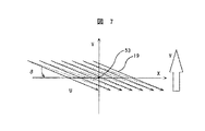
図5から図7に、本発明の第2の実施例を示す。図5,図6は図2と同じく、電子線の走査方向を説明する図であって、試料の電子線が照射される部分の拡大図、図7は図6に対応して電子線の走査偏向方向を説明する模式図である。
【0065】
本実施例と第1の実施例との相違点は、回転ステージ33を有しない点である。その他の構成は第1の実施例と同様であるので、ここでは省略する。
【0066】
図5に示すように、試料9の画像は回転ステージ33を有しないので、X−Y軸に対して角度θだけ回転している場合を想定する。
【0067】
はじめに、第1の実施例と同様に、光学顕微鏡画像あるいは電子線画像から所定の第一の座標と第二の座標の位置補正値、第一の座標に対する第二の座標の回転ずれ量が算出される。この回転ずれ量を電子線の走査偏向位置の補正により補正し、画素あたりの偏向歪み量が最小となる画像を形成する走査方法を説明する。
【0068】
ある特定の比較的小さな領域検査をする場合、ステージが静止した状態で電子線を二次元的に走査し画像を形成する。図5にウエハが回転ずれ量の角度θをもつ場合の二次元走査の方法を示す。制御部6からの指定により、画像取得領域
60の中心53が二次元走査の中心、すなわち光軸54と一致するようにステージを静止させる。この場合、二次元走査の中心は画像取得領域60の幅wの2分の1、長さlの2分の1の位置にある。即ち、電子光学系システム3の光軸54と画像取得領域60の中心53とが一致するように静止させる。
【0069】
図5において、画像取得領域60の幅をw、高さをlとし、直交するX−Y座標系のもとで画像取得領域60の中心53を座標の原点(0,0)とすれば、走査開始点A点が画像取得領域60の座標(−(w/2)cosθ+(l/2)sinθ, (w/2)sinθ+(l/2)cosθ)となるように電子線19を走査偏向器15により偏向し、領域に添って角度θをもって端B点まで走査する。この方向の走査を予め設定された走査ピッチ59(Δp)で一走査ずつずらしながら反復し、座標((w/2)cosθ−(l/2)sinθ,−(w/2)sinθ−(l/2)cosθ)まで走査する。
【0070】
走査に際し、実線で示した一方向のみ電子線19を試料9に照射し、破線で示した電子線19の振り戻しの間は、試料9に電子線19が照射されないようにブランキングすることにより、試料9の上に空間的,時間的に均一に電子線を照射することができる。ブランキングは、ブランキング偏向器13により電子線19を偏向して、絞り14を通過しないようにすることにより実施される。
【0071】
上記走査方法により、画像取得領域に沿った走査が実施され、偏向歪み量が走査中心で振り分けられる為、画像取得領域の走査における総偏向量が最小となり、画素あたりの偏向歪みが最小となる比較検査に適した画像が形成される。
【0072】
広領域をくまなく検査する場合、上記の方法によると、画像取得領域毎に、ステージを静止させて電子線を走査する時間の他に、ステージの移動時間として加速,減速,位置整定を加算した時間がかかり、検査時間全体では長時間を要してしまう。そこで広領域を検査する場合、ステージを一方向に連続的に定速で移動しながら、電子線をステージ移動方向と直交または交叉する向きに高速に一方向に走査することにより、被検査領域の画像を取得する検査方法を用いるとよい。所定距離の一走査幅分の電子線取得時間は、所定距離をステージが移動する時間のみとなる。
【0073】
図6と図7にステージの一軸の連続移動の場合、図8と図9にステージの二軸の連続移動の場合の各々について、以下説明する。
【0074】
はじめに、ステージの一軸の連続移動の場合の、本発明の第3の実施例を、以下説明する。図6において、回転ずれ量の角度θで、ステージの一軸が連続移動する場合、図1に示す制御部6からの指定によってYステージ32をステージ速度vの定速でY方向に移動させた時に、電子光学系システム3の光軸54が画像取得領域60の中心53を通るように、Xステージ31を静止させる。そして、Yステージ32がY方向に連続移動している際に、電子線19を幅w,長さlの矩形領域に沿って走査する。
【0075】
Yステージ32が移動している間、電子線19は画像取得領域60の中心53を中心とした走査を繰り返すので、この時の、電子光学系システム3の光軸54から見た走査パターンは、図7に示すようになる。図7において、光軸54を原点とするX−Y座標系に、画像取得領域60の幅をw,長さをl,走査速度をu,試料9から見たみかけの走査速度をu′とすると、追従角度δは回転ずれθを含み、δ=arcsin((u′/u)sinθ−v/u)となる。ただし、δ,u′,u,θ,vは、各々図7中の矢印の方向を正としている。
【0076】
直交するX−Y座標のもとで光軸54を原点(0,0)とすると、走査開始点A点は、走査中心が座標((l/2)cosθ,0)で、走査幅が(cosθ/cosδ)wとなるように、追従角度δをもってB点まで走査する。しかしながら、ステージ機構により試料を連続移動させながら、画像取得を走査する場合、ステージ移動方向についてはステージ移動の定速性を考慮しなければならない。
【0077】
そこで、図6に示す試料9の上での走査ピッチ59(Δp)を用いて、時間間隔(Δp・sinθ)/v毎に走査の中心をΔp・cosθずつ移動させながら、走査の中心の座標が(−(l/2)cosθ,0)となるまで走査を反復することにより、画像取得領域60を予め設定された走査ピッチ59(Δp)で走査することが可能となる。これらの走査条件は検査装置に予め設定され、図1に示した制御部6により指定される。ステージ速度vは時間経過と共に若干変動するため、その分は画像取得領域60の中心53において、電子線19の光軸54がステージ移動方向にずれることがある。
【0078】
画像取得領域60の走査に際し、図6,図7の実施例において実線で示した一方向のみ、電子線19を試料9に照射する。破線で示した電子線19の振り戻しの間は、試料9に電子線19が照射されないようにブランキングすることにより、試料9上に空間的,時間的に均一に電子線19を照射することができる。ブランキングは、ブランキング偏向器13により電子線19を偏向して、絞り14を通過しないようにすることにより実施される。
【0079】
電子線が照射されている領域または位置は、Xステージ31,Yステージ32に設置された位置モニタ測長器34の測定データが時々刻々と制御部6に転送されることにより、詳細に把握される。同様に、電子線19が照射されている領域あるいは位置の高さの変動は、試料高さ測定器35の測定データが時々刻々と制御部6に転送されることにより詳細に把握される。これらのデータに基づき、電子線19の照射位置や焦点位置のずれを演算し、補正制御回路43によりこれらの位置ずれを自動的に補正する。このようにして、高精度で精密に電子線を走査できるようになる。
【0080】
上記により、画像取得領域に沿った走査が実施され、偏向歪み量が走査中心で振り分けられる為、画像取得領域の走査における総偏向量が最小となって、画素あたりの偏向歪みが最小となり、2画像比較による検査における欠陥の誤った判定を防止できる。
【0081】
つぎに、ステージの二軸の連続移動の場合の、本発明の第4の実施例を説明する。図8は図2と同じく、電子線の走査方向を説明する図であって、試料の電子線が照射される部分の拡大図、図9は図8に対応して電子線の走査偏向方向を説明する模式図である。
【0082】
まず、回転ずれ量の角度θで、ステージの二軸が各々連続移動する場合の走査方法について説明する。
【0083】
図8において、はじめに、幅w,長さlの矩形の画像取得領域60の中心53と電子線19の走査の光軸54とが一致するように、Xステージ31,Yステージ32をステージ速度vで定速移動させる。次に、ステージを移動させながら電子線19を走査する。このとき、図8に示したXステージ31とYステージ32の両方の合成速度であるステージ速度vが、図8に示した電子線19の走査方向55に対して略直角となるように、Xステージ31の速度とYステージ32の速度とを決定する。
【0084】
ここで、実際には、各ステージの移動速度のむら,電子線19の偏向制御のむらによる電子線走査位置のむらが存在し、合成速度vと電子線19の走査方向とのなす角度を厳密に直角にすることは困難であるので、取得画像を用いた欠陥判定に支障の無い精度に保てばよい。
【0085】
さらに、電子線19を走査している間は、Xステージ31,Yステージ32が移動しているので、Xステージ31,Yステージ32の移動を考慮して実際の電子線の走査方向を決定する必要がある。図9に示すように、X軸方向に対しての回転ずれ量の角度θを考慮し、さらに図4で説明した方法で、追従角度δを求め、実際の走査角度を求める。このようにして、電子線19を走査すれば、図3,図4で説明した場合と同様にして、回転ずれ量の角度θが補正された画像を取得することができる。
【0086】
以上の結果、画像取得領域に沿った走査が実施され、偏向歪み量が走査中心で振り分けられる為、画像取得領域の走査における総偏向量が最小となって、画素あたりの偏向歪みが最小となり、2つの画像の比較による検査における欠陥の誤った判定を防止できる。
【0087】
以上のように、本実施例によれば、比較検査に適した、画素あたりの偏向歪みが少ない良質な画像が得られ、誤検出を低減することができ、検査装置としての信頼性を向上させることができる検査方法および検査装置を提供できる。また、本発明になる検査装置を半導体製造プロセスへ適用する事により、異常発生を迅速かつ正確に検知することができるので、多量の不良発生を未然に防止する事ができるという優れた効果をもたらす。さらにその結果、不良の発生そのものを低減させることができるので、半導体装置等の信頼性を高める事が出来、新製品等の開発効率が向上し、かつ製造コストが削減できるという優れた効果をもたらす。
【0088】
【発明の効果】
以上述べたように、本発明によれば、試料台を移動中または停止中に荷電粒子線を走査して得られる試料の画像信号の偏向歪みの影響を少なくして、試料の欠陥を得ることができる荷電粒子線を用いた検査装置および検査方法を得ることができるという効果がある。
【図面の簡単な説明】
【図1】SEM式外観検査装置の装置構成の概略を示す縦断面図。
【図2】電子線が照射される部分の拡大図。
【図3】電子線が照射される部分の拡大図。
【図4】図3に対応して電子線の走査偏向方向を説明する模式図。
【図5】電子線が照射される部分の拡大図。
【図6】電子線が照射される部分の拡大図。
【図7】図6に対応して電子線の走査偏向方向を説明する模式図。
【図8】電子線が照射される部分の拡大図。
【図9】図8に対応して電子線の走査偏向方向を説明する模式図。
【図10】図2における検査の手順を示すフローチャート。
【図11】図3における検査の手順を示すフローチャート。
【符号の説明】
1…SEM式外観検査装置、9…試料、15…走査偏向器、19…電子線、
20…二次電子検出器、31…Xステージ、32…Yステージ、34…位置モニタ測長器、49…欠陥判定部、51…二次電子、52…第二の二次電子、53…中心、54…光軸、55…走査方向、59…ピッチ、60…画像取得領域。
[0001]
TECHNICAL FIELD OF THE INVENTION
The present invention relates to an inspection apparatus and an inspection method for a semiconductor device such as a memory and an LSI having a fine circuit pattern and a circuit pattern such as a liquid crystal and a photomask, and particularly to an inspection apparatus and an inspection method using a charged particle beam.
[0002]
[Prior art]
2. Description of the Related Art A semiconductor device is manufactured by repeating a process of transferring a circuit pattern formed on a semiconductor wafer on a photomask by lithography and etching. The quality of lithography, etching, and other processes in the manufacturing process of a semiconductor device, the generation of foreign matter in the manufacturing process, and the like greatly affect the yield of the semiconductor device. Therefore, in order to detect the occurrence of processing abnormality or defect early or in advance, it is necessary to inspect a pattern formed on a semiconductor wafer in a manufacturing process for each process.
[0003]
In the manufacturing process of a semiconductor device, the pattern is generated by scanning a pattern with a charged particle beam such as an electron beam or an optical visual inspection device for determining an abnormality using an image obtained by irradiating a pattern with a laser beam or the like. Various inspection devices for judging abnormalities from secondary electrons and reflected electrons using signal strength and images are actually used.
[0004]
As an example of an optical inspection apparatus for inspecting a defect existing in a pattern on a semiconductor wafer, a defect inspection apparatus that irradiates a semiconductor wafer with white light and compares the same circuit patterns of a plurality of LSIs using an optical image is known. This is known, and its summary is described in the magazine "Semiconductor World of the Month", August 1995, pp. 96-99.
[0005]
When a semiconductor wafer in a manufacturing process is inspected by such an optical inspection method, a residue or a defect of a pattern having a silicon oxide film or a photosensitive photoresist material on the surface through which light is transmitted cannot be detected. In addition, it was not possible to detect an unetched residue or a non-opening defect in a minute conduction hole, which was lower than the resolution of the optical system. Furthermore, a defect generated at the bottom of the step of the wiring pattern could not be detected.
[0006]
As described above, with the miniaturization of circuit patterns, the complexity of circuit pattern shapes, and the diversification of materials, it has become difficult to detect defects using optical images.Therefore, charged particle beams with higher resolution than optical images, especially electron There has been proposed a method of comparing and inspecting a circuit pattern using an image obtained by scanning a line. When a circuit pattern is compared and inspected using an electron beam image, an image is acquired at a very high speed compared with observation by a scanning electron microscope (SEM) in order to obtain a practical inspection time. There is a need. Then, it is necessary to ensure the resolution of the image acquired at high speed and the SN ratio of the image.
[0007]
As an example of such a pattern comparison inspection apparatus using an electron beam, a document "Journal of Vacuum Science Technology B, Vol. 9, No. 6, pp. 3005 to 3009 (1991)" (J. Vac. Sci. Tech. B, Vol. 9, No. 6, pp. 3005-3009 (1991)), and the document "Journal of Vacuum Science Technology B, Vol. 10, No. 6, Pages 2804 to 2808 (1992) "(J. Vac. Sci. Tech. B, Vol. 10, No. 6, pp. 2804-2808 (1992)), and JP-A-5-258703. And US Pat. No. 5,502,306 disclose an electron beam having an electron beam current 100 times or more (10 nA or more) that of a normal SEM. Is irradiated on a conductive substrate (such as an X-ray mask), and any or a plurality of generated secondary electrons, reflected electrons, and transmitted electrons are detected, and images formed from the signals are compared and inspected to automatically detect defects. A detection method is described.
[0008]
In addition, it is difficult to obtain a high-resolution image due to the space charge effect with a high current and low acceleration electron beam. As a method for solving this problem, Japanese Patent Application Laid-Open No. 5-258703 mentioned above discloses a method of immediately before the sample. Describes a method of decelerating a high-acceleration electron beam and irradiating the sample with a substantially low-acceleration electron beam on a sample.
[0009]
As a method for acquiring an electron beam image at a high speed, a method of continuously irradiating a semiconductor wafer on a sample stage with an electron beam while continuously moving the sample stage is disclosed in JP-A-59-160948 and JP-A-5-160948. -258703.
[0010]
In such an inspection apparatus that irradiates a sample substrate with a finely focused electron beam at a high speed to acquire and inspect an electron beam image, an aberration generated in comparison with the amount of deflection of the electron beam, that is, an acquisition having deflection distortion. Comparing an image with a reference image having no deflection distortion or an acquired image having a deflection distortion different from the previous deflection distortion will result in an erroneous result that there is a defect in a part that is not originally a defect.
[0011]
Regarding this deflection distortion, Japanese Patent Application Laid-Open No. Sho 58-154153 discloses that the stage obtained is moved to a position with respect to the optical axis of the visual field moved by the deflection of the charged particle beam, and the acquired image is degraded by the off-axis deflection. It is stated to prevent. However, when scanning the charged particle beam while continuously moving the sample stage, it is necessary to determine the deflection scanning region of the charged particle beam in consideration of the rotation error of the sample, and there is no description on this point.
[0012]
[Problems to be solved by the invention]
An object of the present invention is to reduce the influence of deflection distortion of an image signal of a sample obtained by scanning a charged particle beam while moving or stopping the sample stage, and to provide a charged particle beam that can obtain a defect of the sample. An object of the present invention is to provide an inspection apparatus and an inspection method used.
[0013]
[Means for Solving the Problems]
In order to achieve the above object, the present invention is to match the optical axis of the charged particle beam with the center of the target area on the sample to be irradiated with the charged particle beam, and to perform the irradiation of the charged particle beam based on the moving speed of the stage. A scanning direction is determined, and then, the sample is irradiated with the charged particle beam while one of the stages is stopped and the other is moved.
[0014]
The present invention also provides an inspection apparatus for extracting a defect by comparing an image of a first region and an image of a second region obtained by scanning with a charged particle beam, wherein the first or the second region When scanning with a charged particle beam a spatially continuous image acquisition region including at least one of the regions, the center of at least one axis in a rectangular coordinate system centered on the optical axis of the charged particle beam is image acquisition. It is provided with a configuration for scanning a charged particle beam so as to pass near the center of the region.
[0015]
BEST MODE FOR CARRYING OUT THE INVENTION
(Example)
Hereinafter, embodiments of the present invention will be described with reference to the drawings.
[0016]
An outline of a configuration of an SEM type visual inspection apparatus for inspecting a pattern of a semiconductor wafer or a mask or a reticle using an electron beam to which the present invention is applied will be described. FIG. 1 is a longitudinal sectional view schematically showing the configuration of the SEM appearance inspection apparatus. The SEM appearance inspection apparatus 1 is roughly divided into an inspection room 2 including an electron optical system system 3, an optical microscope unit 4, and a sample room 8, an image processing unit 5, a control unit 6, and a secondary electron detection unit. 7
[0017]
The electron optical system 3 includes an electron gun 10, an electron beam extraction electrode 11, a condenser lens 12, a blanking deflector 13, a diaphragm 14, a scanning deflector 15, an objective lens 16, a reflection plate 17, and an ExB deflector 18. The sample 9 is irradiated with an electron beam 19 generated by the electron gun 10 and extracted by the extraction electrode 11 through the condenser lens 12, the aperture 14, and the objective lens 16. The electron beam 19 is a narrowed beam, and the sample 9 is scanned by the scanning deflector 15, and reflected electrons and secondary electrons 51 are generated from the sample 9. The secondary electrons have their trajectories bent by the ExB deflector 18 and irradiate the reflecting plate 17 to generate second secondary electrons 52, which are detected by the secondary electron detector 20. On the other hand, by directing the electron beam 19 to the outside of the opening of the stop 14 by the blanking deflector 13, the irradiation of the sample 9 with the electron beam 19 can be prevented.
[0018]
The sample chamber 8 includes a sample stage 30, an X stage 31, a Y stage 32, a rotary stage 33, a position monitor length measuring device 34, and a sample height measuring device 35. The optical microscope unit 4 is installed in a position near the electron optical system 3 in the room of the inspection room 2 so as not to affect each other, and is provided between the electron optical system 3 and the optical microscope unit 4. Is known. The X stage 31 or the Y stage 32 reciprocates a known distance between the electron optical system 3 and the optical microscope unit 4.
[0019]
The optical microscope unit 4 includes a white light source 40, an optical lens 41, and a CCD camera 42. Although not shown, an acquired image is sent to the image processing unit 5 in the same manner as an electron beam image described later.
[0020]
In this embodiment, a length measuring device based on laser interference is used as the position monitor measuring device 34. The positions of the X stage 31, the Y stage 32, and the rotating stage 33 can be monitored in real time, and the position information can be sent to the control unit 6. Although not shown, data such as the number of rotations of the motors of the X stage 31, the Y stage 32, and the rotation stage 33 are also transmitted from the respective drivers to the controller 6. The control unit 6 can accurately grasp the region and position where the electron beam 19 is irradiated based on these data, and corrects the positional deviation of the irradiation position of the electron beam 19 in real time as necessary. The correction can be performed using the control circuit 43. Further, even if the sample 9 is changed, the region irradiated with the electron beam can be stored for each sample.
[0021]
As the sample height measuring device 35, an optical measuring device using a measuring method other than the electron beam, for example, a laser interferometer or a reflected light measuring device for measuring a change in the position of reflected light is used. The configuration is such that the height of the sample 9 mounted on the Y stage 31 can be measured in real time. In the present embodiment, a method in which an elongated white light passing through a slit is applied to a sample 9 through a transparent window, the position of reflected light is detected by a position detection monitor, and a height change amount is calculated from a position change. Was used. Based on the measurement data of the sample height measuring device 35, the focal length of the objective lens 16 for narrowing down the electron beam 19 is dynamically corrected so that the electron beam 19 can be always focused on the inspection area. It has become. Further, it is also possible to configure so that the warpage and the height distortion of the sample 9 are measured in advance before the electron beam irradiation, and the correction conditions for each inspection area of the objective lens 16 are set based on the data. .
[0022]
In order to obtain an image of the sample 9, the electron beam 19 narrowed down is irradiated on the sample 9 to generate secondary electrons 51, which are scanned by the electron beam 19 and moved by the X stage 31 and the Y stage 32. Synchronously detect.
[0023]
The electron beam 19 is extracted from the electron gun 10 by applying a voltage between the electron gun 10 and the extraction electrode 11. The electron beam 19 is accelerated by applying a high negative voltage to the electron gun 10. As a result, the electron beam 19 advances toward the sample stage 30 with energy corresponding to the potential, is converged by the condenser lens 12, is further narrowed down by the objective lens 16, and is narrowed down by the X stage 31 and the Y stage 32 on the sample stage 30. The sample 9 mounted on the rotating stage 33 is irradiated.
[0024]
A scanning signal and a scanning signal generator 44 for generating a blanking signal are connected to the blanking deflector 13, and an objective lens power supply 45 is connected to the objective lens 16. A negative voltage can be applied to the sample 9 by the retarding power supply 36. By adjusting the voltage of the retarding power supply 36, the primary electron beam can be decelerated, and the irradiation energy of the electron beam to the sample 9 can be adjusted to an optimum value without changing the potential of the electron gun 10. When it is necessary to blank the electron beam 19, the electron beam 19 is deflected by the blanking deflector 13, and the electron beam 19 can be controlled so as not to pass through the aperture 14.
[0025]
Secondary electrons 51 generated by irradiating the sample 9 with the electron beam 19 are accelerated by the negative voltage applied to the sample 9. Above the sample 9, an ExB (E-cross-B) deflector 18 is arranged, and the accelerated secondary electrons 51 are deflected in a predetermined direction. The amount of deflection can be adjusted by the voltage applied to the ExB deflector 18 and the strength of the magnetic field. Further, this electromagnetic field can be changed in conjunction with a negative voltage applied to the sample. The secondary electrons 51 deflected by the ExB deflector 18 collide with the reflector 17 under predetermined conditions. The reflection plate 17 has a conical shape, and the electron beam 19 passes through an opening provided at the center thereof. When the accelerated secondary electrons 51 collide with the reflector 17, a second secondary electron 52 having an energy of several V to 50 eV is generated from the reflector 17.
[0026]
The secondary electron detector 20 is disposed above the objective lens 16 in the inspection room 2 and detects the second secondary electrons 52. The output signal of the secondary electron detector 20 is provided outside the inspection room 2. The amplified data is amplified by the preamplifier 21, converted into digital data by the AD converter 22, and transmitted from the light conversion unit 23 to the electric conversion unit 25 of the image processing unit 5 by the light transmission unit 24. When the reflection plate 17 is not provided, the secondary electrons 51 may be detected by the secondary electron detector 20 instead of the second secondary electrons 52.
[0027]
The high-voltage power supply 26 supplies a preamplifier drive power supply 27 for driving the preamplifier 21, an AD converter drive power supply for driving the AD converter 22, and a voltage to be applied to the secondary electron detector 20 to attract the second secondary electrons. Power is supplied to the reverse bias power supply 29. The second secondary electrons 52 generated by colliding with the reflection plate 17 are guided to the secondary electron detector 20 by an attraction electric field generated by the secondary electron detector 20 by the supply of the reverse bias power supply 29.
[0028]
The secondary electron detector 20 detects the secondary electrons 51 generated during the irradiation of the sample 9 with the electron beam 19 and then accelerates and collides with the reflector 17 to generate the second secondary electrons.
52 is configured to be detected in conjunction with the scanning timing of the electron beam 19.
[0029]
The output signal of the secondary electron detector 20 is amplified by a preamplifier 21 installed outside the inspection room 2, and converted into digital data by an AD converter 22. The AD converter 22 is configured to convert an analog signal detected by the secondary electron detector 20 into a digital signal immediately after being amplified by the preamplifier 21 and transmit the digital signal to the image processing unit 5. As described above, since the detected analog signal is digitized and transmitted immediately after the detection, a signal having a high speed and a high SN ratio can be obtained.
[0030]
The sample 9 is mounted on the X stage 31 and the Y stage 32. The X stage 31 and the Y stage 32 are stationary when the inspection is performed, and the electron beam 19 is two-dimensionally scanned when the inspection is performed. , Y stage 32 is continuously moved in the Y direction at a constant speed, and any one of methods of linearly scanning electron beam 19 in the X direction can be selected. The former method is effective for inspecting a specific relatively small area, and the latter method is effective for inspecting a relatively large area.
[0031]
The image processing unit 5 includes a first storage unit 46, a second storage unit 47, a calculation unit 48, a defect determination unit 49, and a monitor 50. The captured electron beam image or optical image is displayed on the monitor 50. Operation commands and operation conditions of each unit of the device are input and output from the control unit 6. In the control unit 6, conditions such as acceleration voltage at the time of electron beam generation, electron beam deflection width, deflection speed, signal fetch timing of the secondary electron detector 20, and moving speed of the sample stage 30 are arbitrarily set according to the purpose. Is entered so that it can be selected or set. The control unit 6 monitors the position and height deviations from the signals of the position monitor length measuring device 34 and the sample height measuring device 35 using the correction control circuit 43, generates a correction signal from the result, and generates an electron beam. The correction signal of the objective lens 16 is sent to the objective lens power supply 45 and the correction signal of the blanking deflector 13 is sent to the scanning signal generator 44 so that 19 is always irradiated to the correct position.
[0032]
The image processing unit 5 includes a first storage unit 46 and a second storage unit 47, a calculation unit 48, a defect determination unit
49, and a monitor 50. The image signal of the sample 9 transmitted by the optical fiber 24 is stored in the first storage unit 46 or the second storage unit 47 after being converted into an electric signal again by the electric conversion unit 25.
[0033]
The arithmetic unit 48 performs positioning of the stored image signal with the image signal of the other storage unit, normalizes the signal level, performs various image processing for removing noise signals, and compares the two image signals. Calculate.
[0034]
The defect judging unit 49 compares the absolute value of the difference image signal calculated by the operation unit 48 with a predetermined threshold value. If the difference image signal level is higher than the predetermined threshold value, the pixel is determined to be defective. The position is determined as a candidate, and the number of defects is displayed on the monitor 50.
[0035]
In the above-described embodiment, the secondary electron detector 20 is applied with the reverse bias voltage from the reverse bias power supply 29. However, the secondary electron detector 20 may be configured not to apply the reverse bias voltage. In the present embodiment, a PIN type semiconductor detector is used as the secondary electron detector 20, but another type of semiconductor detector, for example, a Schottky type semiconductor detector or an avalanche type semiconductor detector may be used. . If conditions such as responsiveness and sensitivity are satisfied, an MCP (micro channel plate) can be used as a detector.
[0036]
Next, a case where a semiconductor wafer subjected to pattern processing in a manufacturing process is inspected by the SEM appearance inspection apparatus 1 shown in FIG. 1 will be described with reference to FIG.
[0037]
The sample 9 is loaded into a sample exchange chamber (not shown). After the sample 9 is mounted on a sample holder (not shown) and held and fixed, the sample exchange chamber is evacuated, and when the sample exchange chamber reaches a certain degree of vacuum, it is transferred to the inspection chamber 2. In the inspection room 2, the sample holder is placed on the sample table 30 via the X stage 31, the Y stage 32, and the rotating stage 33 and held and fixed.
[0038]
The sample 9 is arranged at predetermined first coordinates below the optical microscope unit 4 by moving the X stage 31 and the Y stage 32 in the X and Y directions based on predetermined inspection conditions registered in advance. As a result, an optical microscope image of the circuit pattern formed on the sample 9 is observed. Then, it is compared with an equivalent circuit pattern image stored in advance for position rotation correction, and a position correction value of the first coordinate is calculated. Next, it moves away from the first coordinates by a certain distance, moves to the second coordinates where a circuit pattern equivalent to the first coordinates exists, and similarly observes the optical microscope image and stores it for position rotation correction. The position correction value of the second coordinate and the amount of rotation deviation with respect to the first coordinate are calculated by comparison with the circuit pattern image. The rotation stage 33 is rotated by the calculated rotation deviation amount to correct the rotation.
[0039]
In the present embodiment, the amount of rotation deviation is corrected by the rotation of the rotation stage 33. However, a method of correcting the scanning deflection position of the electron beam based on the calculated amount of rotation deviation without providing the rotation stage 33 is also possible. The amount of rotation deviation can be corrected. This method will be described later.
[0040]
Next, for future position correction, the first coordinate, the amount of displacement of the first circuit pattern by observing the optical microscope image, the second coordinate, the amount of misalignment of the second circuit pattern by observing the optical microscope image. Is stored and sent to the control unit 6.
[0041]
Next, the circuit pattern formed on the sample 9 is observed by an optical microscope, and the position of the chip where the circuit pattern is located, the distance between the chips, or the repetition pitch of a repetition pattern such as a memory cell is measured in advance. The measured value is input to the control unit 6. Further, a chip to be inspected and a region to be inspected in the chip are designated and input to the control unit 6. The image of the optical microscope can be observed at a relatively low magnification, and when the surface of the sample 9 is covered with, for example, a silicon oxide film, the image can be transmitted down to the base and observed. In addition, the arrangement of the chips and the layout of the circuit patterns in the chips can be easily observed, and the region to be inspected can be easily set.
[0042]
When the preparatory work such as the predetermined correction work and the setting of the inspection area by the optical microscope unit 4 is completed as described above, the sample 9 is moved below the electron optical system 3 by the movement of the X stage 31 and the Y stage 32. You. When the sample 9 is placed below the electron optical system 3, the same operation as the correction operation and the setting of the inspection area performed by the optical microscope unit 4 is performed by an electron beam image. The acquisition of the electron beam image at this time is performed by the following method.
[0043]
Based on the coordinate values stored and corrected by the alignment based on the optical microscope image, the electron beam 19 is two-dimensionally scanned in the X and Y directions by the scanning deflector 15 in the same circuit pattern as that observed by the optical microscope unit 4. Is scanned. Due to the two-dimensional scanning of the electron beam, secondary electrons 51 are generated from the observed part, and the second secondary electrons 52 generated by the reflection plate 17 are detected by the secondary electron detector 20 to obtain an electron beam image. Is done. Since simple inspection position confirmation, position alignment, and position adjustment have already been performed using an optical microscope image, and rotation correction has been performed in advance, large adjustment is not required. The electron beam image has a higher resolution than the optical image, and can perform alignment, position correction, and rotation correction with high magnification and high accuracy.
[0044]
Regarding the secondary electron detector 20, in the conventional SEM, a configuration using a scintillator (a phosphor deposited on aluminum), a light guide, and a photomultiplier tube is used. Since this type of detection device detects light emitted by a phosphor, it has poor frequency response and is unsuitable for high-speed electron beam image formation. In order to solve this problem, as a detecting device for detecting a high-frequency secondary electron signal, a detecting means using a semiconductor detector is described in JP-A-2-15545 and JP-A-5-258703. Thus, the embodiment of the present invention also uses a semiconductor detector for high-speed detection.
[0045]
In addition, the method of detecting secondary electrons using the secondary electron detector 20, digitizing the detected image signal immediately after detection, and then transmitting the light, reduces the effect of noise generated in various conversions and transmissions. , Image signal data having a high SN ratio. In the process of forming an electron beam image from the detected signal, the image processing unit 5 applies a detection signal every time corresponding to a desired pixel at the electron beam irradiation position designated by the control unit 6 according to the signal level. The stored brightness gradation values are sequentially stored in the first storage unit 46 or the second storage unit 47. By correlating the electron beam irradiation position with the amount of secondary electrons associated with the detection time, an electron beam image of the circuit pattern of the sample 9 is formed two-dimensionally. In this embodiment, the inspection method and apparatus for detecting secondary electrons generated from the sample have been described. However, backscattered electrons and reflected electrons are generated from the sample simultaneously with the secondary electrons. These secondary charged particles as well as secondary electrons can be similarly detected as electron beam image signals.
[0046]
When the image signal is transferred to the image processing unit 5, the electron beam image of the first area is stored in the first storage unit. The arithmetic unit 48 performs alignment of the stored image signal with the image signal of the other storage unit, normalization of a signal level, and various image processing for removing a noise signal. Subsequently, the electron beam image of the second region is stored in the second storage unit 47, and the same circuit pattern of the electron beam image of the second region and the first electron beam image is obtained while performing the same arithmetic processing. And the image signal at the location are compared. The defect judging unit 49 compares the absolute value of the difference image signal calculated by the operation unit 48 with a predetermined threshold value. If the difference image signal level is higher than the predetermined threshold value, the pixel is determined to be defective. The position is determined as a candidate, and the number of defects is displayed on the monitor 50. Next, thirdly, the electron beam image of the region is stored in the first storage unit 46, and is compared with the electron beam image of the second region previously stored in the second storage unit 47 while performing the same operation. Is determined. Thereafter, by repeating this operation, image processing is performed on all inspection areas.
[0047]
By acquiring a high-precision and high-quality electron beam image by the above-described inspection method and performing comparative inspection, a minute defect generated on a fine circuit pattern can be detected in an inspection time conforming to practicality. In addition, by acquiring an image using an electron beam, light transmitted by the optical pattern inspection method cannot be inspected, and a pattern formed by a silicon oxide film or a resist film, and foreign materials and defects of these materials can be removed. Be able to inspect. Further, the inspection can be stably performed even when the material forming the circuit pattern is an insulator.
[0048]
When the sample 9 is irradiated with the electron beam 19, the portion is charged. In order to avoid the influence of the electrification at the time of the inspection, the circuit pattern to be irradiated with the electron beam 19 in the pre-inspection preparation work such as the position rotation correction or the inspection area setting is selected from circuit patterns existing outside the inspection area in advance. Alternatively, it is preferable that the controller 6 can automatically select an equivalent circuit pattern on a chip other than the chip to be inspected. Thus, the influence of the irradiation of the electron beam 19 does not affect the inspection image. The scanning with the large current electron beam may be performed only once or may be repeated several times.
[0049]
The conditions for irradiating the sample with the electron beam include the irradiation amount of the electron beam per unit area, the current value of the electron beam, the scanning speed of the electron beam, and the irradiation energy of the electron beam irradiating the sample. For these parameters, it is necessary to find the optimum values for each of the shapes and materials of the circuit patterns. For that purpose, it is necessary to freely adjust and control the irradiation energy of the electron beam irradiating the sample. In this embodiment, a retarding power supply
A negative voltage for decelerating the primary electrons of the electron beam 19 is applied by 36, and by adjusting this voltage, the irradiation energy of the electron beam 19 can be appropriately adjusted. When the acceleration voltage applied to the electron gun 10 is changed, a change in the axis of the electron beam 19 occurs and various adjustments are required. In this embodiment, the acceleration voltage applied to the electron gun 10 is not changed. Thus, the irradiation energy of the electron beam 19 can be adjusted.
[0050]
2 to 4 and FIGS. 10 and 11 show a first embodiment of the present invention. 2 and 3 are views for explaining the scanning direction of the electron beam, and are enlarged views of a portion of the sample irradiated with the electron beam, and FIG. 4 is a view for explaining the scanning deflection direction of the electron beam corresponding to FIG. It is a schematic diagram. FIG. 10 is a flowchart showing the procedure of the inspection in FIG. 2, and FIG. 11 is a flowchart showing the procedure of the inspection in FIG.
[0051]
As shown in FIG. 2, when inspecting a certain relatively small inspection area, an image is formed by two-dimensionally scanning the electron beam 19 while the stage is stationary.
[0052]
At the time of scanning, the sample 9 is irradiated with the electron beam 19 in only one direction shown by a solid line, and blanked during the reversal of the electron beam 19 shown by a dashed line.
The sample 19 is not irradiated, and the sample 9 is uniformly and spatially and temporally irradiated with the electron beam 19.
[0053]
This is a case where the electron beam 19 is sequentially scanned from the end in a rectangular area having a width w and a length 1 which is the image acquisition area 60. First, in step 61 of FIG. 10, the angle between the scanning direction of the electron beam 19 and the X-axis direction, that is, the wafer rotation angle θ is detected. Details will be described with reference to FIG. Next, in step 62, the position of the sample 9 is corrected by the rotating stage 33 so that the scanning direction of the electron beam 19 and the X-axis direction match. Next, in step 63, the image acquisition area 60 is set, and in step 64, the center of the image acquisition area 60 is set.
The X stage 31 and the Y stage 32 are stopped by a command from the control unit 6 so that 53 becomes the center of the two-dimensional scanning by the electron beam 19. That is, the sample is stopped so that the optical axis of the electron optical system 3 coincides with the center of the image acquisition area 60, and then an electron beam is scanned to acquire an image.
[0054]
In FIG. 2, the width of the image acquisition area 60 is defined as w, the length is defined as l, and the position of the optical axis and the center 53 of the image acquisition area 60 are coordinate origins (0, 0) under an orthogonal XY coordinate system. 0), the electron beam 19 is deflected by the scanning deflector 15 so that the scanning start point is at the coordinate (-w / 2, l / 2) at the point A at the upper left corner of the image acquisition area 60, and is moved in the X direction. Along the scanning range w from the left end to the right end B of the area. This scanning in the X direction is repeated while shifting one scanning at a time at a pitch 59 (Δp) set in the Y direction, and scanning is performed up to the coordinates (w / 2, −1/2) at the lower right corner. These scanning conditions are set in advance, and are designated by the control unit 6. The above scanning is the step of FIG.
Steps 65 to 69 are performed.
[0055]
When scanning along the image acquisition area 60 is performed by such a scanning method, the amount of deflection distortion is distributed at the scanning center, so that the total amount of deflection in the scan of the image acquisition area 60 is minimized, and the deflection per pixel is reduced. The distortion is minimized, and it is possible to prevent a defect from being erroneously detected in the comparison inspection of the two images.
[0056]
The method shown in FIGS. 3 and 4 is an application of the above method when scanning an electron beam while moving the stage.
[0057]
The semiconductor wafer that is the sample 9 has a diameter of 150 mm to 200 mm, while the width w that can be scanned by the electron beam 19 using a scanning electron microscope (SEM) is at most about several hundred μm. According to the above method, when inspecting all over, it takes time to scan the electron beam while stopping the stage for each image acquisition area, and it takes time to move the stage, and it takes a long time to inspect one semiconductor wafer. Is not suitable. Therefore, a method of shortening the inspection time by scanning the electron beam 19 in one direction at a high speed in a direction orthogonal to or intersecting with the stage movement direction while continuously moving the stage in one direction at a constant speed can be considered. . White arrows indicate stage speed v.
[0058]
In FIG. 3, first, in step 71 of FIG. 11, the angle between the scanning direction of the electron beam 19 and the X-axis direction, that is, the wafer rotation angle θ is detected. The wafer rotation angle θ will be described in detail with reference to FIG. Next, in step 72, the position of the sample 9 is corrected by the rotating stage 33 so that the scanning direction of the electron beam 19 coincides with the X-axis direction. Then, step
At 73, the image acquisition area 60 is set, and at step 74, when the Y stage 32 moves in the Y direction according to an instruction from the control unit 6, the optical axis 54 of the electron beam 19 moves to the center of the image acquisition area 60. The X stage is stopped so as to pass through 53, and the electron beam 19 is scanned by the scanning deflector 44 while the Y stage 32 continuously moves at a constant speed in the Y direction.
[0059]
The scanning of the electron beam 19 viewed from the optical axis of the electron optical system 3 is as shown in FIG. When scanning the image acquisition while continuously moving the sample 9 by the stage mechanism, it is necessary to consider the constant speed of the stage movement in the stage movement direction. Assuming that the width of the image acquisition region 60 is w, the stage speed v scans the sample 9 moving at a constant speed in the Y direction with the electron beam 19 horizontally in the X direction. It is necessary to scan the electron beam 19 with the scanning deflector 15 at a tracking angle δ and a scanning width | w / cos δ | Since the stage speed v slightly changes over time, the optical axis 54 of the electron beam 19 may be shifted in the stage moving direction at the center 53 of the image acquisition area 60 accordingly. The following angle δ is determined by the stage speed v of the Y stage 32 and the scanning speed u of the electron beam. That is, δ = arcsin (v / u). Here, the sign of δ, v, u is positive in the direction of the arrow in FIGS. 3 and 4. The following angle δ may be assumed to be zero if the stage speed v is sufficiently smaller than the scanning speed u.
[0060]
The following calculation of the following angle δ is performed in step 75 of FIG. 11, and scanning is performed in steps 76 to 81.
[0061]
Scanning of the image acquisition area 60 at the set pitch 59 (Δp) is performed by repeating scanning at a time interval Δp / v. These scanning conditions are set in advance and specified by the control unit 6.
[0062]
In the area or position where the electron beam 19 is irradiated, the measurement data measured by the position monitor length measuring device 34 installed on the X stage 31 and the Y stage 32 is transferred to the control unit 6 every moment. Is understood in detail. Similarly, the fluctuation of the height of the region irradiated with the electron beam 19 or the position is described in detail by transferring the measurement data measured by the sample height measuring device 35 to the control unit 6 every moment. To be grasped. Based on these data, the deviation of the irradiation position or the focal position of the electron beam 19 is calculated, and these corrections are automatically corrected by the correction control circuit 43. In this way, the electron beam 19 is controlled with high accuracy and precision.
[0063]
By the above-described scanning method, scanning along the image acquisition area is performed, and the deflection distortion amount is distributed at the scanning center, so that the total deflection amount in scanning the image acquisition area is minimized, and the deflection distortion per pixel is minimized. In addition, it is possible to prevent erroneous determination of a defect in inspection by comparing two images.
[0064]
5 to 7 show a second embodiment of the present invention. 5 and 6 are views for explaining the scanning direction of the electron beam, as in FIG. 2, and are enlarged views of a portion of the sample irradiated with the electron beam. FIG. 7 is a drawing corresponding to FIG. It is a schematic diagram explaining a deflection direction.
[0065]
The difference between the present embodiment and the first embodiment is that the rotary stage 33 is not provided. The other configuration is the same as that of the first embodiment, and will not be described here.
[0066]
As shown in FIG. 5, since the image of the sample 9 does not have the rotating stage 33, it is assumed that the image is rotated by an angle θ with respect to the XY axis.
[0067]
First, similarly to the first embodiment, a position correction value of predetermined first coordinates and a second coordinate, and an amount of rotational displacement of the second coordinates with respect to the first coordinates are calculated from an optical microscope image or an electron beam image. Is done. A description will be given of a scanning method for correcting the rotational deviation amount by correcting the scanning deflection position of the electron beam and forming an image in which the deflection distortion amount per pixel is minimized.
[0068]
When performing a specific relatively small area inspection, an image is formed by two-dimensionally scanning an electron beam while the stage is stationary. FIG. 5 shows a two-dimensional scanning method in the case where the wafer has the angle θ of the rotational shift amount. The image acquisition area is designated by the control unit 6.
The stage is stopped so that the center 53 of the 60 coincides with the center of the two-dimensional scanning, that is, the optical axis 54. In this case, the center of the two-dimensional scanning is located at a position that is a half of the width w of the image acquisition area 60 and a half of the length l. That is, the electronic optical system 3 is stopped so that the optical axis 54 of the electron optical system 3 and the center 53 of the image acquisition area 60 coincide.
[0069]
In FIG. 5, if the width of the image acquisition area 60 is w and the height is 1 and the center 53 of the image acquisition area 60 is the origin (0, 0) of the coordinates under an orthogonal XY coordinate system, The electron beam 19 is scanned and deflected so that the scanning start point A is at the coordinates (− (w / 2) cos θ + (l / 2) sin θ, (w / 2) sin θ + (l / 2) cos θ) of the image acquisition area 60. It is deflected by the detector 15 and scans to the end B at an angle θ along the area. Scanning in this direction is repeated while being shifted by one scan at a preset scanning pitch 59 (Δp), and the coordinates ((w / 2) cos θ− (l / 2) sin θ, − (w / 2) sin θ− (l / 2) Scan to cos θ).
[0070]
During scanning, the sample 9 is irradiated with the electron beam 19 in only one direction indicated by a solid line, and blanking is performed so that the electron beam 19 is not irradiated on the sample 9 during the reversal of the electron beam 19 indicated by a broken line. The electron beam can be uniformly and spatially and temporally irradiated on the sample 9. Blanking is performed by deflecting the electron beam 19 by the blanking deflector 13 so as not to pass through the aperture 14.
[0071]
According to the above-described scanning method, scanning along the image acquisition area is performed, and the amount of deflection distortion is distributed at the scanning center, so that the total amount of deflection in the scanning of the image acquisition area is minimized, and the deflection distortion per pixel is minimized. An image suitable for inspection is formed.
[0072]
When inspecting a wide area, according to the above-described method, acceleration, deceleration, and position setting are added for each image acquisition area in addition to the time for stopping the stage and scanning the electron beam as the movement time of the stage. It takes time, and it takes a long time for the entire inspection time. Therefore, when inspecting a wide area, the electron beam is scanned in one direction at high speed in a direction orthogonal to or crossing the stage movement direction while moving the stage continuously in one direction at a constant speed, thereby obtaining an inspection area. An inspection method that acquires an image may be used. The electron beam acquisition time for one scanning width of the predetermined distance is only the time for the stage to move the predetermined distance.
[0073]
FIGS. 6 and 7 illustrate the case of the single-axis continuous movement of the stage, and FIGS. 8 and 9 illustrate the case of the two-axis continuous movement of the stage.
[0074]
First, the third embodiment of the present invention in the case of continuous movement of one axis of the stage will be described below. In FIG. 6, when one axis of the stage continuously moves at an angle θ of the rotational deviation amount, when the Y stage 32 is moved in the Y direction at a constant stage speed v by the designation from the control unit 6 shown in FIG. Then, the X stage 31 is stopped so that the optical axis 54 of the electron optical system 3 passes through the center 53 of the image acquisition area 60. Then, while the Y stage 32 is continuously moving in the Y direction, the electron beam 19 is scanned along a rectangular area having a width w and a length l.
[0075]
While the Y stage 32 is moving, the electron beam 19 repeats scanning around the center 53 of the image acquisition area 60. At this time, the scanning pattern viewed from the optical axis 54 of the electron optical system 3 is as follows. As shown in FIG. 7, in the XY coordinate system having the optical axis 54 as the origin, the width of the image acquisition area 60 is w, the length is 1, the scanning speed is u, and the apparent scanning speed from the sample 9 is u ′. Then, the following angle δ includes the rotational deviation θ, and δ = arcsin ((u ′ / u) sin θ−v / u). Here, δ, u ′, u, θ, and v each have the positive direction of the arrow in FIG.
[0076]
Assuming that the optical axis 54 is the origin (0, 0) under the orthogonal XY coordinates, the scanning start point A is such that the scanning center is the coordinate ((l / 2) cos θ, 0) and the scanning width is ( (cos θ / cos δ) The scanning is performed up to the point B with the following angle δ so that w. However, when scanning the image acquisition while the sample is continuously moved by the stage mechanism, it is necessary to consider the constant speed of the stage movement in the direction of the stage movement.
[0077]
Then, using the scanning pitch 59 (Δp) on the sample 9 shown in FIG. 6, the coordinates of the scanning center are moved by Δp · cos θ at every time interval (Δp · sin θ) / v, Is repeated until (-(l / 2) cos θ, 0), so that the image acquisition area 60 can be scanned at a preset scanning pitch 59 (Δp). These scanning conditions are set in the inspection apparatus in advance, and designated by the control unit 6 shown in FIG. Since the stage speed v slightly changes with time, the optical axis 54 of the electron beam 19 may be shifted in the stage moving direction at the center 53 of the image acquisition area 60 accordingly.
[0078]
In scanning the image acquisition area 60, the sample 9 is irradiated with the electron beam 19 only in one direction indicated by a solid line in the embodiments of FIGS. During the swingback of the electron beam 19 indicated by the broken line, the sample 9 is blanked so that the electron beam 19 is not irradiated, so that the sample 9 is uniformly and spatially and temporally irradiated with the electron beam 19. Can be. Blanking is performed by deflecting the electron beam 19 by the blanking deflector 13 so as not to pass through the aperture 14.
[0079]
The region or position where the electron beam is irradiated is grasped in detail by transferring the measurement data of the position monitor length measuring device 34 installed on the X stage 31 and the Y stage 32 to the control unit 6 every moment. You. Similarly, the fluctuation of the height of the region or position irradiated with the electron beam 19 can be grasped in detail by transferring the measurement data of the sample height measuring device 35 to the control unit 6 every moment. Based on these data, the deviation of the irradiation position or the focal position of the electron beam 19 is calculated, and these corrections are automatically corrected by the correction control circuit 43. In this way, the electron beam can be scanned with high accuracy and precision.
[0080]
According to the above, scanning along the image acquisition area is performed, and the deflection distortion amount is distributed at the scanning center. Therefore, the total deflection amount in the scanning of the image acquisition area is minimized, and the deflection distortion per pixel is minimized. Erroneous determination of a defect in inspection by image comparison can be prevented.
[0081]
Next, a description will be given of a fourth embodiment of the present invention in the case of continuous movement of the stage in two axes. FIG. 8 is a view for explaining the scanning direction of the electron beam similarly to FIG. 2, and is an enlarged view of a portion of the sample irradiated with the electron beam. FIG. 9 shows the scanning deflection direction of the electron beam corresponding to FIG. It is a schematic diagram explaining.
[0082]
First, a description will be given of a scanning method when the two axes of the stage continuously move at the rotation deviation angle θ.
[0083]
In FIG. 8, first, the X stage 31 and the Y stage 32 are moved to the stage speed v so that the center 53 of the rectangular image acquisition area 60 having the width w and the length l coincides with the optical axis 54 of the scanning of the electron beam 19. To move at a constant speed. Next, the electron beam 19 is scanned while moving the stage. At this time, the stage speed v, which is the combined speed of both the X stage 31 and the Y stage 32 shown in FIG. 8, is substantially perpendicular to the scanning direction 55 of the electron beam 19 shown in FIG. The speed of the stage 31 and the speed of the Y stage 32 are determined.
[0084]
Here, in practice, unevenness in the moving speed of each stage and unevenness in the electron beam scanning position due to unevenness in the deflection control of the electron beam 19 exist. Since it is difficult to perform the defect determination, it is only necessary to maintain the accuracy at which there is no problem in the defect determination using the acquired image.
[0085]
Further, while scanning the electron beam 19, the X stage 31 and the Y stage 32 are moving, so that the actual scanning direction of the electron beam is determined in consideration of the movement of the X stage 31 and the Y stage 32. There is a need. As shown in FIG. 9, the following angle δ is obtained by the method described with reference to FIG. 4 in consideration of the angle θ of the rotational deviation amount with respect to the X-axis direction, and the actual scanning angle is obtained. By scanning the electron beam 19 in this manner, it is possible to obtain an image in which the angle θ of the rotational deviation has been corrected, as in the case described with reference to FIGS.
[0086]
As a result of the above, scanning along the image acquisition area is performed and the deflection distortion amount is distributed at the scanning center, so that the total deflection amount in scanning the image acquisition area is minimized, and the deflection distortion per pixel is minimized, It is possible to prevent erroneous determination of a defect in the inspection by comparing two images.
[0087]
As described above, according to the present embodiment, it is possible to obtain a high-quality image with less deflection distortion per pixel, which is suitable for the comparative inspection, to reduce erroneous detection, and to improve the reliability as an inspection device. An inspection method and an inspection apparatus that can be provided. Further, by applying the inspection apparatus according to the present invention to a semiconductor manufacturing process, it is possible to quickly and accurately detect the occurrence of an abnormality, thereby providing an excellent effect that a large number of defects can be prevented from occurring. . Furthermore, as a result, the occurrence of defects can be reduced, so that the reliability of semiconductor devices and the like can be increased, and the excellent effects of improving the development efficiency of new products and the like and reducing the manufacturing cost can be obtained. .
[0088]
【The invention's effect】
As described above, according to the present invention, it is possible to obtain the defect of the sample by reducing the influence of the deflection distortion of the image signal of the sample obtained by scanning the charged particle beam while moving or stopping the sample stage. There is an effect that an inspection apparatus and an inspection method using a charged particle beam can be obtained.
[Brief description of the drawings]
FIG. 1 is a longitudinal sectional view schematically showing the configuration of a SEM type visual inspection device.
FIG. 2 is an enlarged view of a portion irradiated with an electron beam.
FIG. 3 is an enlarged view of a portion irradiated with an electron beam.
FIG. 4 is a schematic diagram for explaining a scanning deflection direction of an electron beam corresponding to FIG. 3;
FIG. 5 is an enlarged view of a portion irradiated with an electron beam.
FIG. 6 is an enlarged view of a portion irradiated with an electron beam.
FIG. 7 is a schematic diagram illustrating a scanning deflection direction of an electron beam corresponding to FIG.
FIG. 8 is an enlarged view of a portion irradiated with an electron beam.
FIG. 9 is a schematic diagram illustrating the scanning deflection direction of the electron beam corresponding to FIG.
FIG. 10 is a flowchart showing the procedure of the inspection in FIG. 2;
FIG. 11 is a flowchart showing the procedure of the inspection in FIG. 3;
[Explanation of symbols]
1 SEM type visual inspection device, 9 sample, 15 scanning deflector, 19 electron beam,
Reference numeral 20: secondary electron detector, 31: X stage, 32: Y stage, 34: position monitor length measuring instrument, 49: defect determination unit, 51: secondary electron, 52: second secondary electron, 53: center , 54: optical axis, 55: scanning direction, 59: pitch, 60: image acquisition area.

Claims (12)

試料を載置しそれぞれ一方向へ移動可能な2つの部材からなるステージと、荷電粒子線を発生させる荷電粒子源と、該荷電粒子源で発生した荷電粒子線が前記試料へ照射されて発生する二次荷電粒子を検出し画像信号を形成する画像形成手段と、前記荷電粒子線が照射される前記試料上の画像取得領域の中心が前記荷電粒子線による二次元走査の中心となるように前記ステージを静止させ、前記ステージの移動速度と移動方向とに基づいて前記荷電粒子線の照射の走査方向を決定するとともに、直交する二軸方向のうちの一軸に沿って前記試料台を連続移動させながら空間的に連続な画像取得領域を前記荷電粒子線で走査する際、前記画像取得領域の中心が前記荷電粒子線による二次元走査の中心となるように前記荷電粒子線を前記試料に照射して、位置モニタ測長器により測定された前記荷電粒子線が照射されている位置と試料高さ測定器により測定された位置の高さの変動から前記荷電粒子線の照射位置や焦点位置のずれを演算し対物レンズ及びブランキング偏向器へ補正信号を送信して補正しながら画像取得領域に沿った走査をさせる制御手段とを備えたことを特徴とする荷電粒子線を用いた検査装置。A stage composed of two members on each of which a sample is placed and movable in one direction, a charged particle source for generating a charged particle beam, and a charged particle beam generated by the charged particle source is irradiated to the sample and generated. Image forming means for detecting secondary charged particles and forming an image signal, wherein the center of an image acquisition area on the sample irradiated with the charged particle beam is the center of two-dimensional scanning by the charged particle beam. While the stage is stationary , the scanning direction of the irradiation of the charged particle beam is determined based on the moving speed and the moving direction of the stage, and the sample stage is continuously moved along one of two orthogonal biaxial directions. while when scanning spatially continuous image acquisition area by the charged particle beam, irradiation of the charged particle beam so that the center of the image acquisition area is the center of the two-dimensional scanning by said charged particle beam onto the sample To, from changes in the position monitor length meter by have been the height of the charged particle beam is determined by the position and the sample height gauge being irradiated position measurement of the irradiation position and the focal position of the charged particle beam An inspection apparatus using a charged particle beam, comprising: control means for calculating a shift, transmitting a correction signal to an objective lens and a blanking deflector, and performing scanning along an image acquisition area while correcting the correction . 荷電粒子線を発生させる荷電粒子源と、該荷電粒子線をパターンが形成された試料へ集束するレンズ手段と、前記試料を載置する試料台と、該試料台を含む試料を試料室に搬送する搬送手段と、前記荷電粒子線を前記試料上で走査させる荷電粒子線走査手段と、前記試料から発生する二次荷電粒子を検出する検出器と、該検出器からの信号に基づいて前記試料上の第一の領域の荷電粒子線画像信号を形成する画像形成手段と、該荷電粒子線画像信号を記憶する記憶手段と、該記憶手段に記憶された荷電粒子線画像信号を前記試料上の前記第一の領域と同一のパターンが形成された第二の領域の荷電粒子線画像信号とを比較する比較手段と、比較手段の比較結果から前記パターンの欠陥を判別する欠陥判別手段とを備えた荷電粒子線を用いた検査装置において、直交する二軸方向に前記試料台を含む試料を空間的に移動させて静止させ次に前記二軸のうちの一軸に沿って前記試料台を連続移動させ、前記比較手段で比較対象とした前記第一または前記第二の領域のうち少なくとも一つの領域を含んだ空間的に連続な画像取得領域を前記荷電粒子線で走査する際、画像取得領域の中心が前記荷電粒子線による二次元走査の中心となるように前記荷電粒子線を前記試料に照射するとともに、位置モニタ測長器により測定された前記荷電粒子線が照射されている位置と試料高さ測定器により測定された位置の高さの変動から前記荷電粒子線の照射位置や焦点位置のずれを演算し対物レンズ及びブランキング偏向器へ補正信号を送信して補正しながら画像取得領域に沿った走査をさせることを特徴とする荷電粒子線を用いた検査装置。A charged particle source for generating a charged particle beam, lens means for focusing the charged particle beam on a sample on which a pattern is formed, a sample table on which the sample is mounted, and a sample including the sample table transferred to a sample chamber Transporting means, charged particle beam scanning means for scanning the charged particle beam on the sample, a detector for detecting secondary charged particles generated from the sample, and the sample based on a signal from the detector. Image forming means for forming a charged particle beam image signal of the first region above, storage means for storing the charged particle beam image signal, and a charged particle beam image signal stored in the storage means on the sample Comparing means for comparing a charged particle beam image signal of a second area in which the same pattern as the first area is formed, and defect determining means for determining a defect of the pattern from a comparison result of the comparing means. Detection using charged particle beam In the apparatus, a sample containing the sample stage in two perpendicular axial spatially moved by stationary, then allowed to continuously move the sample stage along a uniaxial of said biaxial, compared with the comparison means When scanning a spatially continuous image acquisition area including at least one of the first or second areas targeted by the charged particle beam, the center of the image acquisition area is determined by the charged particle beam. While irradiating the sample with the charged particle beam so as to be the center of two-dimensional scanning , the position where the charged particle beam was measured by a position monitor length measuring device and the position measured by a sample height measuring device were measured. calculating a deviation of the irradiation position and the focal position of the charged particle beam from the variation in the height position to be scanned along an image acquisition area while correcting by sending a correction signal to the objective lens and the blanking deflector Inspection apparatus using a charged particle beam, characterized. 請求項2の記載において、前記第一または前記第二の領域の各々が、別々の前記画像取得領域に含まれることを特徴とする荷電粒子線を用いた検査装置。3. The inspection apparatus according to claim 2, wherein each of the first and second regions is included in a separate one of the image acquisition regions. 請求項3の記載において、前記試料台に前記試料を載置する際の試料の回転量を検出する回転検出手段と、前記回転量を補正する補正手段とを備え、該補正手段により前記試料の回転量を補正して前記画像形成手段により前記画像取得領域の画像を形成することを特徴とする荷電粒子線を用いた検査装置。The device according to claim 3, further comprising: a rotation detecting unit configured to detect a rotation amount of the sample when the sample is placed on the sample stage; and a correction unit configured to correct the rotation amount. An inspection apparatus using a charged particle beam, wherein a rotation amount is corrected and an image of the image acquisition area is formed by the image forming unit. 請求項4の記載において、前記回転量の補正手段は、前記試料台を含む試料を空間的に回転させる回転ステージ機構であることを特徴とする荷電粒子線を用いた検査装置。5. The inspection apparatus according to claim 4, wherein the rotation amount correcting unit is a rotary stage mechanism that spatially rotates the sample including the sample stage. 請求項4の記載において、前記回転量の補正手段は、前記回転量を前記荷電粒子線の走査の方向に基づいて補正することを特徴とする荷電粒子線を用いた検査装置。5. The inspection apparatus according to claim 4, wherein the rotation amount correction unit corrects the rotation amount based on a scanning direction of the charged particle beam. 6. 請求項2の記載において、前記第一または前記第二の領域が一つの前記画像取得領域に含まれることを特徴とする荷電粒子線を用いた検査装置。3. The inspection apparatus according to claim 2, wherein the first or second area is included in one image acquisition area. 請求項7の記載において、前記試料台を空間的に移動させるステージ機構を備え、該ステージ機構による前記試料台の移動に基づいて前記画像取得領域の画像の取得が一組の電子光学系システムにより遂行されることを特徴とする荷電粒子線を用いた検査装置。The apparatus according to claim 7, further comprising a stage mechanism for spatially moving the sample stage, wherein the acquisition of the image of the image acquisition area based on the movement of the sample stage by the stage mechanism is performed by a set of electron optical system. An inspection apparatus using a charged particle beam, which is performed. XステージとYステージと回転ステージとからなるステージと、該ステージに載せられた試料に荷電粒子線を照射する荷電粒子線照射手段と、前記荷電粒子線が照射されて発生する二次電子または該二次電子がさらに反射板に反射して発生する第二の二次電子の少なくともひとつを検出する二次電子検出手段と、該二次電子検出手段によって検出された信号に基づいて前記試料の欠陥を検出する欠陥検出手段とを備えた荷電粒子線を用いた検査装置において、前記荷電粒子線を照射する前記試料上の対象領域の中心を検出する中心検出手段と、該中心検出手段によって検出された中心が前記荷電粒子線による二次元走査の中心となるように前記ステージを静止させる光軸設定手段と、前記対象領域の形状に基づいて前記荷電粒子線の照射の走査方向を決定し、該走査方向に基づいて前記回転ステージを回転させて前記試料の方向を決定する走査方向決定手段とを備え、前記ステージは、直交する二軸方向に前記試料を空間的に移動させて静止させ、前記二軸のうちの一軸に沿って前記試料を連続移動させ、前記荷電粒子線照射手段は前記荷電粒子線を前記走査方向決定手段で決定された前記走査方向へ照射して、位置モニタ測長器により測定された前記荷電粒子線が照射されている位置と試料高さ測定器により測定された位置の高さの変動から前記荷電粒子線の照射位置や焦点位置のずれを演算し対物レンズ及びブランキング偏向器へ補正信号を送信して補正しながら対象領域に沿った走査をさせることを特徴とする荷電粒子線を用いた検査装置。A stage including an X stage, a Y stage, and a rotating stage; charged particle beam irradiation means for irradiating a sample mounted on the stage with a charged particle beam; and secondary electrons generated by irradiating the charged particle beam. Secondary electron detecting means for detecting at least one of the second secondary electrons generated by the secondary electrons being further reflected by the reflecting plate; and a defect of the sample based on a signal detected by the secondary electron detecting means. In the inspection apparatus using a charged particle beam provided with a defect detection means for detecting the center, a center detection means for detecting the center of the target area on the sample irradiated with the charged particle beam, and the optical axis setting means center is still the stage so that the center of the two-dimensional scanning by said charged particle beam, run of the irradiation of the charged particle beam based on the shape of the target region Scanning direction determining means for determining a direction and rotating the rotating stage based on the scanning direction to determine the direction of the sample, wherein the stage spatially moves the sample in orthogonal two-axis directions. is allowed to stand still, along said single axis of biaxially by continuously moving the specimen, the charged particle beam irradiation means irradiates the charged particle beam to said scanning direction determined by said scanning direction determining means The deviation of the irradiation position or the focal position of the charged particle beam from the fluctuation of the position where the charged particle beam is irradiated by the position monitor measuring device and the position measured by the sample height measuring device is changed. An inspection apparatus using a charged particle beam, wherein a scanning is performed along a target area while performing correction by performing a calculation and transmitting a correction signal to an objective lens and a blanking deflector . XステージとYステージと回転ステージとからなるステージに載せられた試料に、荷電粒子線を照射して発生する二次電子または該二次電子がさらに反射板に反射して発生する第二の二次電子の少なくともひとつを検出し、検出された信号に基づいて前記試料の欠陥を検出する荷電粒子線を用いた検査方法において、前記荷電粒子線を照射する前記試料上の画像取得領域の中心が前記荷電粒子線による二次元走査の中心となるように前記ステージを静止させ、前記対象領域の形状に基づいて前記荷電粒子線の照射の走査方向を決定し、該走査方向に基づいて前記回転ステージを回転させ、前記ステージは直交する二軸方向に前記試料を空間的に移動させて静止させ、前記二軸のうちの一軸に沿って前記試料を連続移動させ、前記決定された前記走査方向へ前記荷電粒子線を照射して、位置モニタ測長器により測定された前記荷電粒子線が照射されている位置と試料高さ測定器により測定された位置の高さの変動から前記荷電粒子線の照射位置や焦点位置のずれを演算し対物レンズ及びブランキング偏向器へ補正信号を送信して補正しながら対象領域に沿った走査をさせることを特徴とする荷電粒子線を用いた検査方法。A secondary electron generated by irradiating a sample mounted on a stage including an X stage, a Y stage, and a rotating stage with a charged particle beam, or a secondary electron generated by the secondary electrons being further reflected by a reflector. In an inspection method using a charged particle beam that detects at least one of the secondary electrons and detects a defect of the sample based on the detected signal, a center of an image acquisition area on the sample that irradiates the charged particle beam is The stage is stopped so as to be the center of the two-dimensional scanning by the charged particle beam, a scanning direction of irradiation of the charged particle beam is determined based on a shape of the target area, and the rotating stage is determined based on the scanning direction. the rotate the stage is stationary spatially moving the sample in two orthogonal axial directions, said by continuously moving the sample along one axis of the two-axis, before the determined And irradiating said charged particle beam in the scanning direction, the charged from the height variation of the position measured by the position and sample height measuring device the charged particle beam measured is irradiated by the position monitor length measuring device Inspection using charged particle beam, which calculates the deviation of the irradiation position and focal position of the particle beam, sends a correction signal to the objective lens and blanking deflector, and scans along the target area while correcting Method. XステージとYステージとからなるステージと、該ステージに載せられた試料に荷電粒子線を照射する荷電粒子線照射手段と、前記荷電粒子線が照射されて発生する二次電子または該二次電子がさらに反射板に反射して発生する第二の二次電子の少なくともひとつを検出する二次電子検出手段と、該二次電子検出手段によって検出された信号に基づいて前記試料の欠陥を検出する欠陥検出手段とを備えた荷電粒子線を用いた検査装置において、前記荷電粒子線を照射する前記試料上の対象領域の中心を検出する中心検出手段と、該中心検出手段によって検出された中心が前記荷電粒子線による二次元走査の中心となるように前記ステージを静止させる光軸設定手段と、前記ステージの移動速度と移動方向とに基づいて前記荷電粒子線の照射の走査方向を決定する走査方向決定手段とを備え、前記荷電粒子線照射手段は直交する二軸方向のうちの一軸に沿って前記試料台を連続移動させながら空間的に連続な画像取得領域を前記荷電粒子線で走査して、位置モニタ測長器により測定された前記荷電粒子線が照射されている位置と試料高さ測定器により測定された位置の 高さの変動から前記荷電粒子線の照射位置や焦点位置のずれを演算し対物レンズ及びブランキング偏向器へ補正信号を送信して補正しながら対象領域に沿った走査をさせることを特徴とする荷電粒子線を用いた検査装置。A stage composed of an X stage and a Y stage, charged particle beam irradiation means for irradiating a sample mounted on the stage with a charged particle beam, secondary electrons generated by irradiation of the charged particle beam or the secondary electrons Further detects at least one of the second secondary electrons generated by reflection on the reflection plate, and detects a defect of the sample based on a signal detected by the secondary electron detection means. In an inspection apparatus using a charged particle beam having a defect detection unit, a center detection unit that detects a center of a target region on the sample that irradiates the charged particle beam, and a center detected by the center detection unit is wherein the optical axis setting means for stationary the stage so that the center of the two-dimensional scanning with the charged particle beam, the irradiation of the charged particle beam based on the moving speed and the moving direction of the stage And a scanning direction determining means for determining a査direction, the spatially continuous image acquisition area while continuously moving the sample stage along a single axis of the biaxial direction the charged particle beam irradiation means perpendicular Scanning with a charged particle beam, the irradiation of the charged particle beam based on a change in the height of the position irradiated with the charged particle beam measured by a position monitor length measuring device and the height measured by a sample height measuring device An inspection apparatus using a charged particle beam, which calculates a displacement of a position or a focal position, transmits a correction signal to an objective lens and a blanking deflector, and performs scanning along a target area while performing correction . XステージとYステージとからなるステージに載せられた試料に荷電粒子線を照射し、発生する二次電子または該二次電子がさらに反射板に反射して発生する第二の二次電子の少なくともひとつを検出し、検出した信号に基づいて前記試料の欠陥を検出する荷電粒子線を用いた検査方法において、前記荷電粒子線を照射する前記試料上の画像取得領域の中心が前記荷電粒子線による二次元走査の中心となるように前記ステージを静止させ、前記ステージの移動速度と移動方向とに基づいて前記荷電粒子線の照射の走査方向を決定し、次に、直交する二軸方向のうちの一軸に沿って前記試料台を連続移動させながら空間的に連続な画像取得領域を前記荷電粒子線で走査して、位置モニタ測長器により測定された前記荷電粒子線が照射されている位置と試料高さ測定器により測定された位置の高さの変動から前記荷電粒子線の照射位置や焦点位置のずれを演算し対物レンズ及びブランキング偏向器へ補正信号を送信して補正しながら対象領域に沿った走査をさせることを特徴とする荷電粒子線を用いた検査方法。A sample placed on a stage composed of an X stage and a Y stage is irradiated with a charged particle beam, and at least the secondary electrons generated or the second secondary electrons generated by the secondary electrons being further reflected by a reflecting plate are generated. In the inspection method using a charged particle beam for detecting one and detecting a defect of the sample based on the detected signal, the center of an image acquisition area on the sample irradiated with the charged particle beam is determined by the charged particle beam. The stage is stopped so as to be the center of the two-dimensional scanning, the scanning direction of the irradiation of the charged particle beam is determined based on the moving speed and the moving direction of the stage, and then, of the orthogonal two axial directions, While continuously moving the sample stage along one axis, a spatially continuous image acquisition area is scanned with the charged particle beam, and the charged particle beam measured by a position monitor length measuring device is irradiated. While correcting by sending a correction signal to the location and the sample height from changes in the height of the measured position by the measuring instruments and calculates the deviation of the irradiation position and the focal position of the charged particle beam objective lens and the blanking deflector An inspection method using a charged particle beam, wherein scanning is performed along a target area.
JP32644099A 1998-11-17 1999-11-17 Inspection apparatus and inspection method using charged particle beam Expired - Fee Related JP3601382B2 (en)

Priority Applications (1)

Application Number Priority Date Filing Date Title
JP32644099A JP3601382B2 (en) 1998-11-17 1999-11-17 Inspection apparatus and inspection method using charged particle beam

Applications Claiming Priority (3)

Application Number Priority Date Filing Date Title
JP10-326322 1998-11-17
JP32632298 1998-11-17
JP32644099A JP3601382B2 (en) 1998-11-17 1999-11-17 Inspection apparatus and inspection method using charged particle beam

Publications (2)

Publication Number Publication Date
JP2000215834A JP2000215834A (en) 2000-08-04
JP3601382B2 true JP3601382B2 (en) 2004-12-15

Family

ID=26572150

Family Applications (1)

Application Number Title Priority Date Filing Date
JP32644099A Expired - Fee Related JP3601382B2 (en) 1998-11-17 1999-11-17 Inspection apparatus and inspection method using charged particle beam

Country Status (1)

Country Link
JP (1) JP3601382B2 (en)

Families Citing this family (7)

* Cited by examiner, † Cited by third party
Publication number Priority date Publication date Assignee Title
JP3751841B2 (en) * 2001-02-26 2006-03-01 株式会社日立製作所 Inspection apparatus using electron beam and inspection method using electron beam
JP2004132867A (en) * 2002-10-11 2004-04-30 Shimadzu Corp Substrate inspection device
US9847209B2 (en) 2014-01-13 2017-12-19 Applied Materials Israel Ltd. Inspection of regions of interest using an electron beam system
US9466462B2 (en) 2014-01-13 2016-10-11 Applied Materials Israel Ltd. Inspection of regions of interest using an electron beam system
US10541104B2 (en) 2015-07-09 2020-01-21 Applied Materials Israel Ltd. System and method for scanning an object with an electron beam using overlapping scans and electron beam counter-deflection
US10054551B2 (en) 2016-04-20 2018-08-21 Applied Materials Israel Ltd. Inspection system and method for inspecting a sample by using a plurality of spaced apart beams
KR20230032003A (en) * 2017-09-07 2023-03-07 에이에스엠엘 네델란즈 비.브이. Method of inspecting samples with multiple beams of charged particles

Also Published As

Publication number Publication date
JP2000215834A (en) 2000-08-04

Similar Documents

Publication Publication Date Title
JP3996774B2 (en) Pattern defect inspection method and pattern defect inspection apparatus
US20090309022A1 (en) Apparatus for inspecting a substrate, a method of inspecting a substrate, a scanning electron microscope, and a method of producing an image using a scanning electron microscope
JP3791095B2 (en) Circuit pattern inspection method and inspection apparatus
JP3823073B2 (en) Inspection method and inspection apparatus using electron beam
JP2001313322A (en) Checking method and apparatus by use of charged particle beam
JP4006119B2 (en) Circuit pattern inspection apparatus and circuit pattern inspection method
JP3601382B2 (en) Inspection apparatus and inspection method using charged particle beam
JP2000286310A (en) Method and apparatus for inspecting pattern defects
JP4746659B2 (en) Circuit pattern inspection method
JP5135115B2 (en) Inspection method and inspection apparatus using charged particle beam
JP4274247B2 (en) Circuit pattern inspection method and inspection apparatus
JP3896996B2 (en) Circuit pattern inspection apparatus and inspection method
JP3765988B2 (en) Electron beam visual inspection device
JP2001093950A (en) Method and device for inspecting semiconductor pattern
JP3876668B2 (en) Visual inspection equipment using electron beam
JP3950891B2 (en) Pattern defect inspection method and pattern defect inspection apparatus
US20090261251A1 (en) Inspection apparatus and inspection method
JP3911407B2 (en) Charged particle beam scanning system
JP5372445B2 (en) Scanning electron microscope apparatus and focusing method thereof
JP3608451B2 (en) Inspection apparatus and inspection method using a scanning electron microscope
JP4317765B2 (en) Inspection method and inspection apparatus using charged particle beam
JP2003346695A (en) Electron beam type pattern inspecting apparatus and inspection method using electron beam
JP2004157135A (en) Method of and apparatus for inspecting circuit pattern
JP5135116B2 (en) Inspection method and inspection apparatus using charged particle beam
JP2000164661A (en) Inspection device of circuit pattern

Legal Events

Date Code Title Description
A977 Report on retrieval

Free format text: JAPANESE INTERMEDIATE CODE: A971007

Effective date: 20040206

A131 Notification of reasons for refusal

Free format text: JAPANESE INTERMEDIATE CODE: A131

Effective date: 20040330

A521 Written amendment

Free format text: JAPANESE INTERMEDIATE CODE: A523

Effective date: 20040527

A131 Notification of reasons for refusal

Free format text: JAPANESE INTERMEDIATE CODE: A131

Effective date: 20040615

A521 Written amendment

Free format text: JAPANESE INTERMEDIATE CODE: A523

Effective date: 20040811

TRDD Decision of grant or rejection written
A01 Written decision to grant a patent or to grant a registration (utility model)

Free format text: JAPANESE INTERMEDIATE CODE: A01

Effective date: 20040831

A61 First payment of annual fees (during grant procedure)

Free format text: JAPANESE INTERMEDIATE CODE: A61

Effective date: 20040913

FPAY Renewal fee payment (event date is renewal date of database)

Free format text: PAYMENT UNTIL: 20081001

Year of fee payment: 4

FPAY Renewal fee payment (event date is renewal date of database)

Free format text: PAYMENT UNTIL: 20091001

Year of fee payment: 5

FPAY Renewal fee payment (event date is renewal date of database)

Free format text: PAYMENT UNTIL: 20101001

Year of fee payment: 6

FPAY Renewal fee payment (event date is renewal date of database)

Free format text: PAYMENT UNTIL: 20111001

Year of fee payment: 7

FPAY Renewal fee payment (event date is renewal date of database)

Free format text: PAYMENT UNTIL: 20121001

Year of fee payment: 8

FPAY Renewal fee payment (event date is renewal date of database)

Free format text: PAYMENT UNTIL: 20131001

Year of fee payment: 9

LAPS Cancellation because of no payment of annual fees