JP3599564B2 - Ion flow forming method and apparatus - Google Patents
Ion flow forming method and apparatus Download PDFInfo
- Publication number
- JP3599564B2 JP3599564B2 JP17884098A JP17884098A JP3599564B2 JP 3599564 B2 JP3599564 B2 JP 3599564B2 JP 17884098 A JP17884098 A JP 17884098A JP 17884098 A JP17884098 A JP 17884098A JP 3599564 B2 JP3599564 B2 JP 3599564B2
- Authority
- JP
- Japan
- Prior art keywords
- plasma
- ion
- ions
- ion flow
- flow forming
- Prior art date
- Legal status (The legal status is an assumption and is not a legal conclusion. Google has not performed a legal analysis and makes no representation as to the accuracy of the status listed.)
- Expired - Fee Related
Links
Images


Classifications
-
- C—CHEMISTRY; METALLURGY
- C23—COATING METALLIC MATERIAL; COATING MATERIAL WITH METALLIC MATERIAL; CHEMICAL SURFACE TREATMENT; DIFFUSION TREATMENT OF METALLIC MATERIAL; COATING BY VACUUM EVAPORATION, BY SPUTTERING, BY ION IMPLANTATION OR BY CHEMICAL VAPOUR DEPOSITION, IN GENERAL; INHIBITING CORROSION OF METALLIC MATERIAL OR INCRUSTATION IN GENERAL
- C23C—COATING METALLIC MATERIAL; COATING MATERIAL WITH METALLIC MATERIAL; SURFACE TREATMENT OF METALLIC MATERIAL BY DIFFUSION INTO THE SURFACE, BY CHEMICAL CONVERSION OR SUBSTITUTION; COATING BY VACUUM EVAPORATION, BY SPUTTERING, BY ION IMPLANTATION OR BY CHEMICAL VAPOUR DEPOSITION, IN GENERAL
- C23C16/00—Chemical coating by decomposition of gaseous compounds, without leaving reaction products of surface material in the coating, i.e. chemical vapour deposition [CVD] processes
- C23C16/44—Chemical coating by decomposition of gaseous compounds, without leaving reaction products of surface material in the coating, i.e. chemical vapour deposition [CVD] processes characterised by the method of coating
- C23C16/50—Chemical coating by decomposition of gaseous compounds, without leaving reaction products of surface material in the coating, i.e. chemical vapour deposition [CVD] processes characterised by the method of coating using electric discharges
- C23C16/515—Chemical coating by decomposition of gaseous compounds, without leaving reaction products of surface material in the coating, i.e. chemical vapour deposition [CVD] processes characterised by the method of coating using electric discharges using pulsed discharges
-
- C—CHEMISTRY; METALLURGY
- C23—COATING METALLIC MATERIAL; COATING MATERIAL WITH METALLIC MATERIAL; CHEMICAL SURFACE TREATMENT; DIFFUSION TREATMENT OF METALLIC MATERIAL; COATING BY VACUUM EVAPORATION, BY SPUTTERING, BY ION IMPLANTATION OR BY CHEMICAL VAPOUR DEPOSITION, IN GENERAL; INHIBITING CORROSION OF METALLIC MATERIAL OR INCRUSTATION IN GENERAL
- C23C—COATING METALLIC MATERIAL; COATING MATERIAL WITH METALLIC MATERIAL; SURFACE TREATMENT OF METALLIC MATERIAL BY DIFFUSION INTO THE SURFACE, BY CHEMICAL CONVERSION OR SUBSTITUTION; COATING BY VACUUM EVAPORATION, BY SPUTTERING, BY ION IMPLANTATION OR BY CHEMICAL VAPOUR DEPOSITION, IN GENERAL
- C23C16/00—Chemical coating by decomposition of gaseous compounds, without leaving reaction products of surface material in the coating, i.e. chemical vapour deposition [CVD] processes
- C23C16/44—Chemical coating by decomposition of gaseous compounds, without leaving reaction products of surface material in the coating, i.e. chemical vapour deposition [CVD] processes characterised by the method of coating
- C23C16/50—Chemical coating by decomposition of gaseous compounds, without leaving reaction products of surface material in the coating, i.e. chemical vapour deposition [CVD] processes characterised by the method of coating using electric discharges
- C23C16/511—Chemical coating by decomposition of gaseous compounds, without leaving reaction products of surface material in the coating, i.e. chemical vapour deposition [CVD] processes characterised by the method of coating using electric discharges using microwave discharges
-
- H—ELECTRICITY
- H01—ELECTRIC ELEMENTS
- H01J—ELECTRIC DISCHARGE TUBES OR DISCHARGE LAMPS
- H01J37/00—Discharge tubes with provision for introducing objects or material to be exposed to the discharge, e.g. for the purpose of examination or processing thereof
- H01J37/32—Gas-filled discharge tubes
- H01J37/32009—Arrangements for generation of plasma specially adapted for examination or treatment of objects, e.g. plasma sources
- H01J37/32192—Microwave generated discharge
-
- H—ELECTRICITY
- H01—ELECTRIC ELEMENTS
- H01J—ELECTRIC DISCHARGE TUBES OR DISCHARGE LAMPS
- H01J37/00—Discharge tubes with provision for introducing objects or material to be exposed to the discharge, e.g. for the purpose of examination or processing thereof
- H01J37/32—Gas-filled discharge tubes
- H01J37/32009—Arrangements for generation of plasma specially adapted for examination or treatment of objects, e.g. plasma sources
- H01J37/32357—Generation remote from the workpiece, e.g. down-stream
-
- H—ELECTRICITY
- H01—ELECTRIC ELEMENTS
- H01J—ELECTRIC DISCHARGE TUBES OR DISCHARGE LAMPS
- H01J37/00—Discharge tubes with provision for introducing objects or material to be exposed to the discharge, e.g. for the purpose of examination or processing thereof
- H01J37/32—Gas-filled discharge tubes
- H01J37/32009—Arrangements for generation of plasma specially adapted for examination or treatment of objects, e.g. plasma sources
- H01J37/32422—Arrangement for selecting ions or species in the plasma
Landscapes
- Chemical & Material Sciences (AREA)
- Engineering & Computer Science (AREA)
- Physics & Mathematics (AREA)
- Plasma & Fusion (AREA)
- Analytical Chemistry (AREA)
- Materials Engineering (AREA)
- Chemical Kinetics & Catalysis (AREA)
- Mechanical Engineering (AREA)
- Metallurgy (AREA)
- Organic Chemistry (AREA)
- General Chemical & Material Sciences (AREA)
- Electron Sources, Ion Sources (AREA)
- Plasma Technology (AREA)
Description
【0001】
【発明の属する技術分野】
本発明は,プラズマ装置に関する。
【0002】
さらに,本発明は,例えばプラズマ処理装置において,正イオンのみをプラズマから引き出し,電子や負イオンはプラズマ側に追い返し,被処理物に向かう正イオン流を形成する方法及び装置に関する。
【0003】
【従来の技術】
従来より,プラズマ処理装置としては,プラズマエッチング装置,プラズマCVD装置,プラズマアッシング装置,プラズマクリーニング装置などが,広く知られている。これらのプラズマ処理装置(以下,プラズマ装置という)としては,平行平板型のプラズマ処理装置のようにプラズマ発生室とプラズマ処理室が一体化されている装置,及びECRプラズマ装置のようにプラズマ発生室とプラズマ処理室とが分離された装置とがある。
【0004】
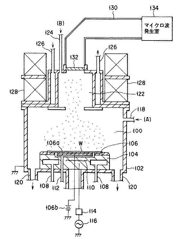
このプラズマ発生室とプラズマ処理室とが分離されたプラズマ装置においては,プラズマ発生室で形成されたプラズマを,或いはプラズマ中の荷電粒子(例.イオン)をプラズマ処理室に導く機構が必要である。図6にはECRプラズマエッチング装置が示されている。ECRプラズマエッチング装置において,処理室100は、気密で開閉自在な処理容器102内に形成されている。この処理容器102内に載置台104が設置され、この載置台104上に静電チャック106などの吸着手段を介して被処理体W(例.半導体ウェハ,LCDガラス基板など)が載置されている。静電チャック106は、ポリイミド樹脂などの絶縁素材性の薄膜間に板状電極106aを装着したもので、この板状電極106aに直流電源106bより高圧電力を印加することによって、ウェハWはクーロン力により載置台に吸着される。
【0005】
載置台104には、ウェハWを所定の温度に調節するために,冷却装置108や、ヒータ110などからなる温度調節手段が設けられている。載置台104内には伝熱ガス供給手段112が設けられており、静電チャック106上の複数の孔から伝熱ガス(例.へリウムガス)がウエハWの裏面から供給され,載置台104からウェハWに至る伝熱効率が高められる。載置台104には、マッチング回路114を介して高周波電源116が接続され,バイアス用高周波電力が載置台に印加される。
【0006】
上記処理容器102の上部側壁には、処理室100内へ所定の処理ガス(例.フッ化炭素ガス、酸素ガス及びアルゴンガスなどの混合ガス)Aを導入するための導入管118が設けられている。上記処理容器102の下部には,真空引き手段(不図示)に通じる排気管120が接続されている。
【0007】
上記処理室100の上部には、ECRプラズマを発生するプラズマ発生室122が連結されている。このプラズマ発生室122には,導波管130を介して,マイクロ波発生室134が連結されている。上記プラズマ発生室122の上壁には、プラズマ発生用のガス(例.アルゴンガス)Bを導入するための導入管124が設けられている。処理室100及びプラズマ発生室122内の気体は,該真空引き手段によって上記排気管120を介して排気されるとともに,上記導入管118及び124から所定の処理ガスが、上記各室に導入される。
上記プラズマ発生室122の側壁裏面部には、冷却手段126が設けられており、上記プラズマ発生室122内で発生した熱は放熱される。さらに、冷却手段126の外部には、磁気コイル128がプラズマ発生室122を取り囲むように設けられている。
【0008】
上記プラズマ発生室122には、マイクロ波を伝搬するための導波管130を介してマイクロ波発生室134が接続されている。マイクロ波発生室134のマグネトロン(不図示)により発振されたマイクロ波(例.2.45GHzのマイクロ波)は導波管130および絶緑壁132を介して,該プラズマ発生室122に伝搬される。該プラズマ発生室122内において、この伝搬されたマイクロ波により放電が励起される。該プラズマ発生室122内には,磁気コイル128により例えば875ガウスの磁界が与えられ、該放電中で電子はサイクロトロン運動し,プラズマ発生用ガスBのECRプラズマが生成される。
【0009】
上記処理室内には,所定の処理ガスAが導入されているため,上記プラズマ発生室122内で生じたプラズマ(電子)の作用により,処理ガス中の反応ガスは解離してラジカルが生じる。
【0010】
一方上記処理室100内の載置台104には,高周波電源116からエッチング回路114を介してバイアス用高周波電力が印加され,さらに上記処理室100内は,排気管120を介して排気されているため,上記プラズマ発生室122内で生じたプラズマ及び該ラジカルは,上記載置台104上に誘導される。上記載置台104上に載置されたウエハW上の被処理膜(例.シリコン酸化膜)は,これらプラズマ及び該ラジカルによりエッチングされる。
【0011】
このECRプラズマ処理装置は、従来の平行平板型プラズマ処理装置などと比較して、被処理体の高度な微細加工に適した装置である。このECRプラズマ処理装置は、異方性エッチングから完全等方性エッチングまでのエッチング形状を制御することが容易である。さらに,イオン化率が高いため、低イオンエネルギーで損傷の少ない高速エッチングが可能である。さらに,処理室内では無電極放電を利用するため、汚染が少ない。
【0012】
このような,プラズマ発生室とプラズマ処理室とが分離されたプラズマ処理装置においては,そのプラズマ処理の効率を高める上から,プラズマ発生室で形成したプラズマ中のイオンを処理室内に効率良く引き出すことが必要である。しかしながら,図6に示されたような装置においては,プラズマ発生室からは,プラズマ処理に必要なイオンのみならず電子も同時に拡散して引き出され,プラズマ処理室内の被処理体に導入される。
【0013】
それらイオンと電子との間には,電気的中性状態を維持するべく力が働いているため,それらを分離し,イオンのみを処理室に効率よく導入することは非常に困難である。電子とイオン(荷電粒子)が混在している状態において,電極を組み合わせた機構により,荷電粒子のみを制御することは容易ではない。この点から,プラズマからイオンのみを分離することの利点が生ずる。プラズマイオン源においては,プラズマからイオンのみを分離して取り出すことは前提条件である。プラズマCVDでは高エネルギーの入射イオンは膜を緻密にするよい働きもする。しかし,イオンのエネルギーが高すぎたり量が多すぎると逆に膜に多くの損傷を与えるという欠点も生ずる。別の観点では,イオンは成膜速度を上昇させる効果も及ぼす(ion induced deposition)。しかしイオンエッチングの効果が大きすぎると,下地にある異なる膜も削られ,汚染の原因にもなる。従って,いずれにしても入射イオンエネルギーの制御は重要な問題である。イオン源においては当然ながら,入射イオンエネルギーの制御は必須である。
【0014】
さらに,図6に示されたような装置において,電子と混在したイオンを所望の状態に制御,すなわちイオンを所望の方向に入射させることは困難である。このため,プラズマ処理室内に所定の電界を発生させる電界発生手段などの各種のイオンの流れを制御する手段が必要である。
【0015】
【発明が解決しようとする課題】
本発明は,プラズマ発生機構で形成されたプラズマから,イオンを効果的に引き出し,該イオンをウエーハ(基板)に向けることを目的とする。
【0016】
さらに,本発明は,プラズマ発生室とプラズマ処理室とが分離されたプラズマ処理装置において,プラズマ発生機構で形成されたプラズマから,イオンを効果的に引き出し,該イオンを被処理物に向けることを目的とする。
【0017】
本発明は,従来のプラズマ処理装置及びそのプラズマ処理方法における,上記のような問題点を解決することを目的する。
【0018】
本発明は,プラズマ発生室内で発生されたプラズマ中のイオンのみを選択的にプラズマ処理室内に向け,該イオンによって被処理物を効率良く処理することを目的とする。
【0019】
さらに,本発明は,相対的に少ない電力で相対的に多くのイオンを引き出すことが可能な,新規かつ改良されたイオン流形成方法及び導入装置を提供することを目的とする。
【0020】
【課題を解決するための手段】
イオンを引き出す箇所に継続的に一定の電位勾配をかけ続けた場合,以下の問題点がある。自由運動を経て電極上に達したイオンは,ある程度引き出しの為の力を受け始める。従ってイオンは電子に引きずられるような逆方向の力をも受ける。このためにこの場合には,イオンはなかなか引き出せない。本発明は,電極間で以下のような操作を反復することにより,この問題を解決する。
【0021】
1)両極性拡散(熱的拡散):電位勾配なし
2)電化分離(イオン加速):電位勾配つき
電極間に導入されたプラズマからイオンのみが効率的に荷電分離される。
【0022】
本発明により形成されたイオン流れは,種々の用途に使用され得る。例えば,インプランテーション用には,径が絞ぼられたイオン流が使用され得る。成膜 (ECR CVD)用には,径が広げられたイオン流が使用され得る。
【0023】
本願発明の第1番目の観点に従って,(a) プラズマ拡散出口を有するプラズマ発生室内にプラズマを発生させる工程と;(b) 該プラズマ発生室内で発生されたプラズマを拡散により、プラズマ発生室の外に配置した2つの電極の間の空間に移動させる拡散工程と;
(c) 該プラズマ発生室の外に移動した該プラズマに,プラズマ中の電子はプラズマ拡散出口の方向に戻し,該プラズマ中のイオンはその逆の方向に引き出す作用を及ぼす向きの電界を該両工程に比して短時間印加する,イオン引き出し工程と;及び
(d) 該引き出されたイオンを被処理物に向けるイオン流形成工程と,
を具備することを特徴とする,プラズマ発生室内で発生されたプラズマからイオンを引き出し,該イオンの流を形成するイオン流形成方法が提供される。
【0024】
本願発明の第2番目の観点に従って,上記第1番目の観点に従ったイオン流形成方法において,該工程(a) 乃至(d) が,この順序で反復して実施されることを特徴とする,イオン流形成方法が提供される。
本願発明の第3番目の観点に従って,上記第1番目の観点に従ったイオン流形成方法において,
該工程(a)が,常時実施されることを特徴とする,イオン流形成方法が提供される。
【0025】
本願発明の第4番目の観点に従って,上記第1番目の観点に従ったイオン流形成方法において,
該イオン引き出し工程(c) は,該プラズマ発生室のプラズマ拡散出口に設置された,2つの電極に異なる電圧を印加することにより実施されることを特徴とする,イオン流形成方法,が提供される。
【0026】
本願発明の第5番目の観点に従って,上記第4番目の観点に従ったイオン流形成方法において,
該イオン引き出し工程(c) は,該プラズマ発生室のプラズマ拡散出口に設置された,2つの電極に異なる電圧をパルス状に印加することにより実施され,
該イオン流形成工程(d) は,該イオンが該二つの電極間の空間から引き出された後で,該2つの電極への該電圧の印加を停止することにより実施される,ことを特徴とするイオン流形成方法が提供される。
【0027】
本願発明の第6番目の観点に従って,上記第1及び3のいずれか一つの観点に従ったイオン流形成方法において,
該工程(b) と該工程(c) との間に,該工程(c) よりはるかに短い時間の工程 (e)を含み,
該工程(e)では,イオンを制御対象として第1電極に,該工程(c)とは逆方向の電界が生じるようにバイアスが印加される,ことを特徴とする方法が提供される。
本願発明の第7番目の観点に従って,上記第1及び3のいずれか一つの観点に従ったイオン流形成方法において,
該イオン流形成工程(d) は,さらに,該2つの電極と被処理物との間に設置された第3の電極に,イオン加速用の電圧及びイオンビーム収束用の電圧の内の少なくとも一つを印加することにより実施される,ことを特徴とするイオン流形成方法が提供される。
【0028】
本願発明の第8番目の観点に従って,上記第4の観点に従ったイオン流形成方法において,
該イオン流形成工程(d) は,該イオンが該2つの電極から被処理物に至る経路において,該イオンの流れを分散する工程,を備えていることを特徴とするイオン流形成方法が提供される。
【0029】
本願発明の第9番目の観点に従って,上記第8の観点に従ったイオン流形成方法において,
該工程(c) は,該イオンに所定の質量とは異なる質量を有するイオンが含まれる場合においては,イオン加速時間/プラズマ拡散時間のパルス比を変更せずに周期を周波数変調及び振幅変調のいずれか一つで変更することにより,該異なる質量のイオンも引出す,ことを特徴とするイオン流形成方法が提供される。
【0030】
本願発明の第10番目の観点に従って,上記第1,4,及び5のいずれか一つの観点に従ったイオン流形成方法において,
イオン流形成工程(d) において,該引き出されたイオンが向けられる被処理物は回路パターンが形成されたシリコンウエハである,ことを特徴とするイオン流形成方法が提供される。
【0031】
本願発明の第11番目の観点に従って,上記第1,4,及び5のいずれか一つの観点に従ったイオン流形成方法において,
プラズマを発生させる工程(a) は,電子サイクロトロン共鳴によりプラズマを発生する工程である,ことを特徴とするイオン流形成方法が提供される。
【0032】
本願発明の第12番目の観点に従って,上記第11の観点に従ったイオン流形成方法において,
該イオン引き出し工程(c) においては,ECRプラズマ形成用のマイクロ波の導入及び外部磁場の少なくとも一つを遮断する,ことを特徴とするイオン流形成方法が提供される。
本願発明の第13番目の観点に従って,
プラズマ拡散出口を有するプラズマ発生室と;
該プラズマ拡散出口に対抗して配置された,被処理物を収容した処理室と;
該プラズマ発生室の該プラズマ拡散出口と,該処理室内の被処理物との間に配置された,2つの電極と;
該2つの電極の電位を制御する電位制御装置であって,該電位制御装置は,
該プラズマ発生室内で発生されたプラズマを拡散により該プラ ズマ発生室の外に配置した2つの電極の間の空間に移動させる拡 散工程においては,該2つの電極の電位は,等電位になるように, 制御し;
該プラズマ発生室の外に拡散し,該2つの電極間の空間に移動 した該プラズマに,プラズマ中の電子はプラズマ発生室の方向に 戻し,該プラズマ中のイオンは処理室の方向に引き出すイオン引 き出し工程においては,該イオン引き出し工程が実施され得るよ うな電界が該2つの電極間の空間に形成されるように,該2つの 電極にパルス状に異なる電圧を印加し;及び
該引き出されたイオンを処理室に収容された被処理物に向ける イオン流れ形成工程においては,該引き出されたイオンが該プラ ズマ中に再度引き戻される作用を及ぼす電界が生じないように, 該電極の電位を制御する,
ことを特徴とする,プラズマ発生室内で発生されたプラズマからイオンを引き出し,該イオンの流を形成する,ことを特徴とするイオン流形成装置が提供される。
【0033】
本願発明の第14番目の観点に従って,上記第13の観点に従ったイオン流形成装置において,該プラズマの発生と,該プラズマの拡散と,イオンの引き出しと,及びイオン流れ形成とが順に反復されることを特徴とするイオン流形成装置が提供される。
【0034】
本願発明の第16番目の観点に従って,上記第14及び15のいずれか一つの観点に従ったイオン流形成装置において,
該拡散工程と,該イオン引き出し工程の間に,該拡散工程よりはるかに短い時間の工程を含み,
該短い時間の工程では,イオンを制御対象として第1電極に,該イオン引き出し工程とは逆方向の電界を生じるようにバイアスが印加される,ことを特徴とする装置が提供される。
【0035】
本願発明の第17番目の観点に従って,上記第13の観点に従ったイオン流形成装置において,
該電位制御装置は,該二つの電極に加えて,プラズマ発生室,及び処理室の電位をも制御することを特徴とする,イオン流形成装置が提供される。
【0036】
本願発明の第18番目の観点に従って,上記第13の観点に従ったイオン流形成装置において,
該被処理物を収容した処理室は,
該電極と被処理物との間に,イオンの流れを分散させるための電極を備える,ことを特徴とする,イオン流形成装置が提供される。
【0037】
本願発明の第19番目の観点に従って,上記第18の観点に従ったイオン流形成装置において,該イオン流は,イオンインプランテーション以外の処理のために使用される,ことを特徴とする,イオン流形成装置が提供される。
【0038】
本願発明の第21番目の観点に従って,上記第13の観点に従ったイオン流形成装置において,
該電極sは,荷電粒子が通過する開口部に近付く程その厚さが薄くされている,ことを特徴とするイオン流形成装置が提供される。
【0039】
本願発明の第22番目の観点に従って,上記第13の観点に従ったイオン流形成装置において,
該イオン流れ形成工程は,該イオンに所定の質量とは異なる質量を有するイオンが含まれる場合においては,イオン加速時間/プラズマ拡散時間のパルス比を変更せずに周期を周波数変調及び振幅変調のいずれか一つで変更することにより,該異なる質量のイオンも引出す,ことを特徴とするイオン流形成装置が提供される。
本願発明の第23番目の観点に従って,上記第1,14,及び15のいずれか一つの観点に従ったイオン流形成装置において,該処理室に収容される被処理物はシリコンウエハである,ことを特徴とするイオン流形成装置が提供される。 本願発明の第24番目の観点に従って,上記第11,14,及び15のいずれか一つの観点に従ったイオン流形成装置において,該処理室に収容される被処理物は回路パターンが形成されたシリコンウエハである,ことを特徴とするイオン流形成装置が提供される。
【0040】
本願発明の第25番目の観点に従って,上記第11,14,及び15のいずれか一つの観点に従ったイオン流形成装置において,該プラズマ発生室は,電子サイクロトロン共鳴によりプラズマを発生する機構を備た,ことを特徴とするイオン流形成装置が提供される。
【0041】
本願発明の第26番目の観点に従って,上記第11,14,及び15のいずれか一つの観点に従ったイオン流形成装置において,
該プラズマ発生室は,電子サイクロトロン共鳴によりプラズマを発生する機構を備え,
イオン引き出しにおいては,ECRプラズマ形成用のマイクル波の導入及び外部磁場の印加の少なくとも一つ遮断することを特徴とするイオン流形成装置が提供される。
【0042】
【発明の実施の形態】
従来のプラズマ処理装置において,プラズマ発生室で形成されたプラズマを処理室に導入することによる,上述した課題を解決するために,本発明においては,プラズマ発生室で形成されたプラズマ中のイオンは,後述されるイオン流形成装置により,引き出され,該イオンは処理室に導入され,被処理物に向けられる。さらに,本願発明においては,上記イオン流形成装置により,プラズマ中の電子はイオンとは逆の方向に戻され,すなわちプラズマ発生室に戻され,プラズマ発生室でのプラズマの発生効率は向上される。
【0043】
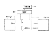
図1を参照して,本願発明のイオン流形成方法及び装置におけるイオン流形成機構を説明する。
プラズマ室202はプラズマ発生機構(図には示されていない)と,該プラズマ発生機構により発生されたプラズマが室外に両極性拡散(イオン,電子及びラジカルが共存された状態での拡散)するためのプラズマ拡散出口203を備えている。
【0044】
プラズマ室202に対する位置に,イオン導入口205を備えた処理室204が設置される。この処理室内には,被処理物が収容されている。
【0045】
これらプラズマ室202と処理室204の間に,荷電粒子が通過し得る2つの電極(第1電極206,第2電極208)が設置される。これらの電極は,荷電粒子が通過し得る電極であればいずれの構造の電極でも採用されうる。例えば,第1電極206として図示された電極のように,その中央部に a開口を有する電極や,第2電極208として図示された電極のように,多数の小開口を有する電極が採用されうる。
【0046】
これらの第1及び第2電極206,208には,制御装置209による制御の下で,電圧源218から電圧が印加される。この電圧源218と制御装置209とにより電位制御装置が構成される。プラズマ発生室と処理室の外壁面を該電圧源218に接続し,制御装置209により,これらプラズマ発生室と処理室の外壁面の電位も制御することも可能である。これらプラズマ室202,第1電極206,第2電極208,処理室204の配置は,一例であって,他の配置も採用されることができる。例えば,プラズマ室202のプラズマ拡散出口203と処理室204のイオン導入口205とを接近又は密着させ,第1電極206及び第2電極208は処理室204の内に設置されることもできる。
【0047】
図1に示されたイオン流形成機構では,下記のステップ(a)〜(d)が繰り返し実施される。
【0048】
ステップ(a)では,プラズマ発生室202にプラズマが形成される。プラズマ発生室202はプラズマ発生用のガス(図6のガスB)が導入され,上記されたプラズマ発生機構により該ガスのプラズマが形成される。このプラズマ発生機構は,前述されたように,高周波電力を使用する方式,マイクロ波を使用する方式,電子サイクロトロン共鳴(ECR)を使用する方式など,プラズマを発生するためのいずれの方式も採用され得る。このプラズマ発生工程においては,プラズマ発生室202,第1電極206,第2電極208の各電圧は,同電位とされ得る。これにより,プラズマ発生室内に形成されるプラズマは,プラズマ拡散口に向かって両極性拡散する。
【0049】
ステップ(b)では,プラズマ発生室202内に形成されたプラズマが拡散する。該プラズマは,プラズマ拡散口203を出て,該プラズマ発生室202と該第1電極206との間の空間にゆっくりと拡散し,次いで第1電極206と第2電極208との間の空間に拡散する。この拡散のために,上記両空間は電界が形成されていない環境とされるのが好ましい。このために,プラズマ発生室202,第1電極206,第2電極208及び処理室204は同電位(例.接地電位)とされる。プラズマ発生室202内に形成されたプラズマは,イオン,電子及びラジカルを含んでいるが,該プラズマは,これらイオン,電子及びラジカルが共存した状態で分子拡散(両極性拡散)する。
【0050】
次のステップ(c)で,プラズマからイオンを効率良く引出すために,該プラズマは上記空間内に十分拡散されることが重要である。このためには,該プラズマ中のイオンと電子が再結合せず一種のアフターグローが継続する程度の拡散時間が確保されることが必要である。この拡散時間(To )は,実験により設定することもできるが,係数を無視して下記の式により概算することも可能である。
To =Lo /v (1)
v2 =kTi /mi (2)
ここで、 To …拡散時間
Lo …イオンの電極間への進入距離
v …熱速度
Ti …イオン温度
k …Boltzmann 定数
mi …イオンの質量
ステップ(c)では,該プラズマからイオンが引き出される。上記両グリツド電極間に到達したプラズマ中のイオンは,その電荷により電子と引きつけ合い,電子とは分かれにくい傾向を持つ。イオンは電子を引きずりながら移動しようとする。従って,熱エネルギ−による拡散によって上記両電極間の空間に「迷い込んだ」プラズマ中のイオンが,載置台に印加されるバイアス電位により加速され,処理室に引き出される効率は低く,プラズマからイオンが効率良く引き出されることは難しい。以上の状況は,金属から電子を引き出す際には仕事関数の値だけ余計にエネルギーを必要とするという状況と類似しているものと考えられる。
【0051】
本発明は,このプラズマから,イオンを効率良く引出すために,上記両電極間にパルス状に電界を形成する。このため,電圧源218から,第1電極206と第2電極208には,図2に示されるような大きさの,パルス制御されたイオン引き出し用電圧が供給される。ここで,Vc ,V1 ,V2 ,Vs は,図1に示すように,プラズマ発生室,第1電極,第2電極,及び処理室の各々に印加されるパルス制御された電位である。また,Zc は引き出し口の位置(チャンバ−(chamber) ),Z1 及びZ2 は電極1及び電極2の位置,Zs はウエハ(基板)の位置である。図2において,(Zc,Vc),(Z1,V1 ) ,(Z2,V2 ) 及び(Zs,Vc)を辿るケース1においては(Vc =Vs ),イオン加速時間は短すぎても長すぎてもよくない。(Zc,Vc),(Z1,V1 ) ,(Z2,V2 ) 及び(Zs,V2 ) を辿るケース2においては(V2 =Vs ),加速時間は長すぎても問題はない。これらのイオン引き出し用電圧が各部に供給されることにより,イオンは第2電極208の方に引きつけられ,電子は第1電極206の方に引きつけられる力が作用するような電界が両電極間に形成される。パルス状に制御されたこれら電圧により,瞬間的に形成された該電界の作用により,該プラズマ中のイオンと電子は,容易かつ効率的に引き離されイオンは第2電極に向け加速され,該第2電極を通過して処理室204のイオン導入口に導かれる。
【0052】
すなわち,イオンを引き出す箇所に継続的に一定の電位勾配をかけ続けた場合,以下の問題点がある。自由運動を経て電極上に達したイオンは,ある程度引き出しの為の力を受け始める。従ってイオンは電子に引きずられるような逆方向の力をも受ける。このために,この場合には,イオンはなかなか引き出せないこととなる。本発明は,電極間で以下のような操作を反復することにより,この課題を解決する。
【0053】
1)両極性拡散(熱的拡散):電位勾配なし
2)電化分離(イオン加速):電位勾配つき
電極間に導入されたプラズマからイオンのみが効率的に荷電分離される。
【0054】
一方,プラズマ中の電子群は,第1電極とプラズマ発生室との間の空間において,両端の電極に印加された電圧(Vc ,V1)により形成された電界の作用により,拡大分散することなくプラズマ拡散出口203に追い返される。従って,電子はプラズマ発生室のプラズマ拡散出口の縁に衝突することなく,プラズマ発生室内に追い返される。電子がプラズマ発生室内に追い返される結果,プラズマ発生室内の電子密度は高くなり,プラズマ発生機構によりプラズマが発生される効率が向上する。また,この電子密度が高くなることから,プラズマ発生室の電位(Vc)は変化する。しかし,第1電極206に印加された正電位(V1 )による電子が戻される効果自体は大きく変化しない。
【0055】
ステップ(d)では,処理室204のイオン導入口に導かれたイオンが被処理物に入射せしめられる。ステップ(c)において,プラズマから引出され,第2電極に向けて加速されたイオンは,第2電極を通過し,処理室204のイオン導入口205に向かう。イオンが第2電極からイオン導入口205に向かう期間,第2電極208の電位V2 と処理室(及び被処理物)の電位Vsが図2に示されたレベルに維持されると,このV2 とVs により形成される電界の作用により,第2電極208を通過したイオンは,減速される。従って,イオンが最高速度近辺に達した時点(例.該イオンの集団が第2電極を通過した直後の時点)で,上記電界を消すか,該イオンをイオン流導入口に加速する方向の電界を形成することが必要である。少なくとも電圧V2 とVsを同電位にすることで,上記電界は消されることができるが,他の電圧Vc,V1 からの影響も無くす観点からは,これら全部位の電圧Vc,V1 ,V2 及びVsを同電位にすることが好ましい。また,該イオンをイオン導入口に加速する方向の電界を形成するために,電圧V2 はVsよりも高い電位とすることができる。
【0056】
このように,上記電界を消すか,逆の方向の電界を形成することにより,イオンは電界による減速を受けることなく,被処理物に入射される。この過程で,或いは電子のエネルギー分布の高いェネルギー成分が電極によって形成されるポテンシャル障壁を越えることによって,被処理物の表面に電子がある程度チャージアップしても,後に入射されるイオンにより,該電子は中和される。イオンのみが選択的にウェハに入射されることから,電子によってイオンの入射方向が乱されることはない。また,入射されるイオンが電子と再結合して消滅することがなく,イオン密度が増加するためウェハを均−に処理することができる。
【0057】
ここで,上記工程(a)乃至(d)を,さらに詳細に説明する。
【0058】
上記ステップ(a)において,上記プラズマ発生機構は,プラズマを発生させる機構のいずれの機構も採用され得る。例えば,高周波プラズマ発生機構,容量結合型プラズマ発生機構,平行平板型プラズマ発生機構,誘導結合型プラズマ発生機構,マイクロ波プラズマ発生機構,ECRプラズマ発生機構など,も採用され得るが,特に図6が参照されて説明されたECRプラズマ発生機構は,好ましい機構の一つである。
【0059】
上記ステップ(b)において,充分にプラズマが生成された状態で,マイクロ波などの導入を中止する(磁場印加を中止する)ことにより,自由な状態で該プラズマを拡散させることもできる。
【0060】
上記ステップ(c)において,プラズマからイオンが引出される間,プラズマ発生用のマイクロ波などがプラズマ発生室に導入されない(例.磁場印加を中止する)ようにすることもできる。
【0061】
上記工程(b)の拡散による移動時間と,工程(c)の電界加速のための時間の2種類の時間の比は,イオンの質量に依存せず,イオン温度(熱速度)とバイアス電圧のみによって決定される。従って,任意のイオンに関して,イオン温度とバイアス電圧による同一のパラメータにより,パルス状バイアス電圧の時間比を決定できる。このため,パルス状のバイアス電圧の制御方法が簡単化される。従って,異なる質量のイオンが混合している場合には,波形を変えずに周波数及び/又は振幅を変調させる制御を行うこともできる。重いイオンに対しては大振幅長周期の変調中の瞬間が有効となる。
【0062】
上記ステップ(d)において,第2電極208又は処理室(被処理物)のどちらかに,負の電位が印加されることができる。第2電極208に負の電位が印加される場合,ここから被処理物までのイオンの運動を,第三の電極110(図3参照)により制御して,イオンの被処理物への入射方向を変更することができる。被処理物に負の電位を印加する場合,電極間で加速されたイオンは何回か互いに衝突する圧力領域を採用する場合が多い。しかし,電子は分離されているため,再結合は殆ど生じない。起きても荷電変換程度である。第三の電極110にバイアス電圧を印加する場合,電界加速のない状態を基礎としないと,そのバイアス電位が設定され難い。
【0063】
上記ステップ(d)において,イオンの入射方向を分散させる為の電極構造として,異なった電位を有する2種類の針状電極306を,図4に示されるように,交互に配置することもできる。ここで白丸○の針状電極は定電位を保持するための電極であり,黒丸●の針状電極はイオンを引きつける為の電極である。イオンを引きつける工程では,電極電位は負電位に固定する。こうすれば電極表面のイオン引き付け効果は弱まらない。それは負電荷を持つ電子が,負電位の電極と反発するためである。一方,イオンを跳ね返す工程では電極は正電位に保たれる。この場合,イオンと電極は反発し合うので,イオンによる電極のスパッタエッチングは少ない。
【0064】
この電極構造の例としては,B−C 間の電極は紙面の前後方向にイオン軌道を振るための電極とし,c−D 間の電極は紙面上の左右の方向にイオン軌道を振るための電極とされることができる。各電極の電位は,V1 =Vc (c=chamber),V2 =Vs (s=substrate),○=V2 ,●=V3 ,V1 〉V2 〉V3 とされることができる。また,V2 〈V3 とされることもできる。
【0065】
また,電子は処理室に侵入することなく,プラズマ発生室に追い返され,プラズマ発生室の電子密度は高められるから,プラズマ発生室内での電離度が増加し,プラズマの生成効率が高められる。
【0066】
上記工程(a)乃至(d)は,所定時間間隔で反復される。この反復時間は,拡散領域内に電子,イオンを伴ったプラズマが十分に拡散する時間と,拡散領域内のイオンのみを選択的に効率よく引き出すことができる時間とから算出され,設定される。そして,例えばイオン引き出し工程(c)の時間がプラズマ拡散工程の時間よりも相対的に短く設定されることにより,拡散領域内に電子,イオンを伴ったプラズマが所望の状態で拡散され,かつ効率よくイオンが第2電極208の方向に引き出される。
【0067】
パルス状制御を止め,イオン引き出し工程の時間をプラズマ拡散工程の時間と同程度にとると処理時間が約2倍になるという欠点が生ずる。
【0068】
第1電極と第2電極の間にイオン引き出し用の電位が印加され,プラズマ中よりイオンが引き出されるに要する時間(T1 ) は,下記の式で求められる。
【0069】
T1 2 =2Lg /a (3)
a=(e/mi )(V/Lg ) (ただし,Lo 〈Lg )(4)
ここで,T1 …プラズマ中よりイオンが引き出されるに要する時間
Lg …電極間距離
a…イオンの加速度
e…素電荷(1.6×10⁻¹⁹ (c) )
mi…イオンの質量
V…バイアス(加速)電圧
プラズマの拡散時間(T0 )とプラズマ中よりイオンが引き出されるに要する時間(T1 )との時間比(相対的パルス幅)は,下記の式で求められる。
【0070】
Mi …イオンの質量
e …素電荷
V …バイアス(加速)電圧
k …Boltzmann 定数
Lo …イオンの電極間への進入距離
Ti …イオン温度
第1電極206と第2電極208間に印加されるパルス制御されたイオン引き出し電圧の相対的パルス幅の下限値は,イオンの質量には,依存しない。実施のパルス幅の設定に当たっては,どの程度までイオンを電極間に進入させるのかという判断に従って係数Lg /Lo の値を変化させれば良い。以上の2種類の距離Lg ,Lo をはっきりと区別すればパルス幅は範囲を持ったものとして導出される。パルス幅の周波数の下限は電極間距離などにもよるが,おおよそ3〜10KHz となる。従って,100KHz程度の値に設定しても,この値は特に大きすぎることはない。
【0071】
イオン引き出し用バイアスVと,”電界加速のための時間(T1 )/熱拡散による移動時間(To)“の比の数値例を下記に示す。
【0072】
【表1】
以上のように,本発明に関わるイオン流形成機構の一つの実施の形態が説明された。次に,他の実施の形態として,このイオン流形成機構が採用されたプラズマ処理装置が説明される。このイオン流形成機構は,種々の形式のプラズマ処理装置,種々の被処理物を処理するプラズマ処理装置に採用されることができる。ここでは,典型的な実施の形態として,半導体ウエハ上に薄膜を形成するための,ECRプラズマ薄膜形成装置を説明する。
図5を参照して,同図に示されたECRプラズマ薄膜形成装置は,その処理室204内に,図1に示されたような第1電極206と第2電極208が設置され,これらの電極には制御装置により制御される電源(図5には示されていない)が接続される。さらに,該電源はプラズマ発生室と処理室にも接続され,これら両室に所定の電圧を印加することもできる。このECRプラズマ薄膜形成装置は,これら電極,制御装置,及び電源以外は,基本的に図6に示された装置と略同一の構成となっている。
【0074】
制御装置による制御の下で,電源から第1電極206と第2電極208(さらには,プラズマ発生室と処理室)への電圧は,制御装置により,同期して供給される。
【0075】
プラズマ処理時には,図1で説明されたと同様の下記のステップが実施される。
【0076】
ステップ(a)では,プラズマ発生室202にプラズマが形成される。
【0077】
ステップ(b)では,プラズマ発生室202内に形成されたプラズマが拡散する。制御装置によって,第1電極206,及び第2電極208には,電圧は印加されない。これらの電極間には電界が無く,プラズマはが両極性拡散する環境が形成される。この環境は,プラズマが両電極間に充分に拡散する時間,維持される。
【0078】
ステップ(c)では,該プラズマからイオンが引き出される。ステップ(b)で,両電極間にプラズマが充分に拡散した後,第1グリット電極206と第2電極208とに,プラズマからイオンを引出すための電圧が印加される。その結果,該プラズマから引出されたイオンは第2電極208の方に加速され,電子は第1電極206の方に戻される。
【0079】
ステップ(d)では,処理室204のイオン導入口に導かれたイオンが被処理物に入射せしめられる。該プラズマから引出され,第2電極208の方に加速されたイオンは,プラズマ室の壁と処理対象物の電位が同一にされた場合には,第2電極を通過した後,第2電極により形成された電界の作用で,第2電極の方に引き戻される方向の作用を受ける。この作用を無くするために,イオンの集団が第2グリッド電極を通過した後,第1電極206及び第2電極208への電圧の印加を中止することができる。
【0080】
上記(a)〜(d)の工程により,処理室へはイオンのみが導入されるから,処理室内での薄膜形成,エッチングなどの処理は,イオンの振る舞いのみに注目して制御されれば良く,該制御は正確に実行されることができる。薄膜形成においては,入射イオン密度を高くするために,基板に不要に大きなバイアスを掛ける必要がなくなる。
【0081】
この実施の形態においては,イオンを被処理物に導く為に,さらに第3電極 (図には示されていない)が設けられる得る。イオンは第3電極を通過した後,該第3電極には,該電源からイオンを被処理物に向かわせる作用を生じるような電圧が印加される。
【0082】
また,イオンの流れ方向を分散させる為の電極構造として,図4に示されるような,異なった電位を有する2種類の針状電極306を,交互に配置することもできる。
【0083】
本発明にかかわるイオン流形成機構が採用された結果,上記実施の形態におけるECRプラズマ薄膜形成装置では,プラズマ中のイオンと電子を効果的に分離でき,プラズマから効率よくイオンは引き出され,高密度のイオンは所望の入射角度で被処理物に入射される。
【0084】
また,プラズマから分離された電子は再びプラズマ発生室内に戻されるため,プラズマ発生室202にはさらに多くの電子が供給され,高密度プラズマを発生させることができる。プラズマ拡散工程(b)に対して,イオン引き出し工程 (d)を相対的に短時間でパルス的に処理することができるため,必要とする量のイオンが短期間に確保されることができ,なめらかな波形による制御と比較して,スループットは向上されることができる。
【0085】
プラズマ処理室内に配置された被処理物は,高密度のイオンのみにより所望の均−な処理を施されることができる。イオンはウエハー上の溝や穴のようなパターンの肩を削り,堆積速度を向上させる働きする。処理室内に導入されたプラズマ中のラジカルは電界の影響を受けずに拡散されつづける。該ラジカルは,イオンによって活性化された被処理物の表面上に比較的ゆっくりと付着していく。電極電位制御の1周期の処理によって被処理物の表面上に処理ガス成分が堆積する量は10原子層未満であり,多くて数原子層である。表面反応確率,すなわち付着係数が小さい場合には,1原子層以下の場合も充分に想定される。すなわち,大部分の粒子がイオンによって活性化された面上に到達する現象が想定される。このため,被処理物の表面上に処理ガス成分が付着する率がイオンによって充分に向上される。従って,被処理物の表面上に効率良く薄膜が形成される。
【0086】
以上,本発明の好適な実施の形態について,添付図面を参照しながら説明したが,本発明はかかる構成に限定されない。
【0087】
例えば,上記実施の形態において,パルス制御されたイオン引き出し用電圧とイオン加速用電圧が使用されたが,本発明はかかる構成に限定されるものではなく,例えば半波整流された交流電力を用いても本発明は実施可能である。従って,本発明において,プラズマからイオンを引出すために印加するパルス状の電界は,矩形的にパルス状の電界が好ましいが,これにかぎられるものではない。矩形状でなくとも,所定の期間中継続する電圧であればよく,半波整流された交流電力により形成される電界などでもよい。
【0088】
さらに,上記実施の形態において,半導体ウェハの表面に薄膜を形成するECRプラズマ薄膜形成装置が説明された。本発明はかかる実施の形態にに限定されるものではなく,例えば,プラズマエッチング装置,プラズマスパッタ装置やイオン注入装置などの各種のプラズマ処理装置に適用されることができる。また,被処理物に関しても,シリコンウエハに限らず,LCD用ガラス基板などの電子部品なども処理されることもできる。
【0089】
さらなる特徴及び変更は,当該技術分野の当業者には着想されるところである。それゆえに,本発明はより広い観点に立つものであり,特定の詳細な及びここに開示された代表的な実施例に限定されるものではない。したがって,添付されたクレームに定義された広い発明概念及びその均等物の解釈と範囲において,そこから離れることなく,種々の変更を行うことができる。
【図面の簡単な説明】
【図1】本発明に関するイオン流形成装置を示した概略的な説明図である。
【図2】図1に示したイオン流形成装置において,イオン引き出し工程において各電極等に印加する電圧を示した図である。
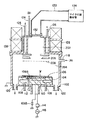
【図3】図1に示したイオン流形成装置に,さらに第3電極が配置された装置の概略的な説明図である。
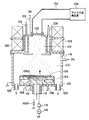
【図4】図1に示したイオン流形成装置に,さらにイオンを分散させる装置が配置された装置の概略的な説明図である。
【図5】図1に示したイオン流形成機構が適用されたECRプラズマ薄膜形成装置の概略的な説明図である。
【図6】関連技術としての,ECRプラズマ薄膜形成装置の概略的な説明図である。
【符号の説明】
102…処理容器, 104…載置台, 108…冷却装置,
110…ヒータ,116…高周波電源,114…マッチング回路,
120…排気管,124…導入管,128…磁気コイル,130…導波管
132…絶縁壁,134…プラズマ波発生室
202…プラズマ発生室,203…プラズマ拡散出口,204…処理室,
205…イオ 導入口,206…第1電極,208…第2電極,
209…制御装置,218…電圧源, 306…針状電極[0001]
TECHNICAL FIELD OF THE INVENTION
The present invention relates to a plasma device.
[0002]
Further, the present invention relates to a method and an apparatus for extracting only positive ions from plasma and for purging electrons and negative ions to the plasma side to form a positive ion flow toward an object to be processed, for example, in a plasma processing apparatus.
[0003]
[Prior art]
Conventionally, as a plasma processing apparatus, a plasma etching apparatus, a plasma CVD apparatus, a plasma ashing apparatus, a plasma cleaning apparatus and the like have been widely known. These plasma processing apparatuses (hereinafter, referred to as plasma apparatuses) include apparatuses in which a plasma generation chamber is integrated with a plasma processing chamber such as a parallel plate type plasma processing apparatus, and plasma generation chambers such as an ECR plasma apparatus. And a plasma processing chamber.
[0004]
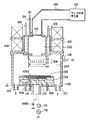
In a plasma apparatus in which the plasma generation chamber and the plasma processing chamber are separated from each other, a mechanism that guides plasma formed in the plasma generation chamber or charged particles (eg, ions) in the plasma to the plasma processing chamber is required. . FIG. 6 shows an ECR plasma etching apparatus. Processing room in ECR plasma etching equipment100Is formed in an airtight and freely openable and
[0005]
In order to adjust the temperature of the wafer W to a predetermined temperature, the mounting table 104 is provided with a temperature adjusting unit including a
[0006]
A processing chamber is provided on the upper side wall of the processing container 102.
[0007]
The above processing chamber100A plasma generation chamber that generates ECR plasma122Are connected. This plasma generation chamber122Is connected to a
The above plasma generation chamber122A cooling means 126 is provided on the rear surface of the side wall of the plasma generation chamber.122The heat generated inside is dissipated. Further, a
[0008]
The above plasma generation chamber122Is connected to a
[0009]
Since a predetermined processing gas A is introduced into the processing chamber, the plasma generation chamber122The reaction gas in the processing gas is dissociated by the action of the plasma (electrons) generated in the inside to generate radicals.
[0010]
Meanwhile, the processing chamber100A high frequency power for bias is applied from a high
[0011]
This ECR plasma processing apparatus is an apparatus suitable for advanced fine processing of an object to be processed, as compared with a conventional parallel plate type plasma processing apparatus or the like. This ECR plasma processing apparatus can easily control the etching shape from anisotropic etching to complete isotropic etching. Further, since the ionization rate is high, high-speed etching with low ion energy and less damage can be performed. Further, since electrodeless discharge is used in the processing chamber, there is little contamination.
[0012]
In such a plasma processing apparatus in which the plasma generation chamber is separated from the plasma processing chamber, ions in the plasma formed in the plasma generation chamber must be efficiently extracted into the processing chamber in order to increase the efficiency of the plasma processing. is necessary. However, in the apparatus as shown in FIG. 6, not only ions necessary for plasma processing but also electrons are diffused and extracted from the plasma generation chamber at the same time, and are introduced into the object to be processed in the plasma processing chamber.
[0013]
Since a force acts between the ions and the electrons to maintain an electrically neutral state, it is very difficult to separate them and to introduce only the ions efficiently into the processing chamber. In a state where electrons and ions (charged particles) are mixed, it is not easy to control only charged particles by a mechanism combining electrodes. This has the advantage of separating only the ions from the plasma. In a plasma ion source, it is a precondition that only ions are separated and extracted from the plasma. In plasma CVD, incident ions of high energy also have a good function of densifying the film. However, if the energy of the ions is too high or the amount is too large, there is a disadvantage that the membrane is damaged much. In another aspect, ions also have the effect of increasing the deposition rate. However, if the effect of the ion etching is too large, a different film on the base is also cut off, which causes contamination. Therefore, in any case, control of the incident ion energy is an important issue. Of course, in an ion source, control of incident ion energy is essential.
[0014]
Further, in the apparatus as shown in FIG. 6, it is difficult to control ions mixed with electrons to a desired state, that is, to make ions incident in a desired direction. Therefore, means for controlling the flow of various ions, such as an electric field generating means for generating a predetermined electric field in the plasma processing chamber, is required.
[0015]
[Problems to be solved by the invention]
An object of the present invention is to effectively extract ions from plasma formed by a plasma generating mechanism and direct the ions to a wafer (substrate).
[0016]
Further, in the present invention, in a plasma processing apparatus in which a plasma generation chamber and a plasma processing chamber are separated, ions are effectively extracted from plasma formed by a plasma generation mechanism, and the ions are directed to an object to be processed. Aim.
[0017]
An object of the present invention is to solve the above-mentioned problems in the conventional plasma processing apparatus and the conventional plasma processing method.
[0018]
SUMMARY OF THE INVENTION It is an object of the present invention to selectively direct only ions in plasma generated in a plasma generation chamber into a plasma processing chamber, and to efficiently process an object to be processed by the ions.
[0019]
It is a further object of the present invention to provide a new and improved ion flow forming method and introducing apparatus capable of extracting relatively many ions with relatively little power.
[0020]
[Means for Solving the Problems]
When a constant potential gradient is continuously applied to a portion from which ions are extracted, the following problems occur. Ions that reach the electrode through free movement begin to receive a certain force for extraction. Thus, the ions are also subjected to the opposite force as dragged by the electrons. Therefore, in this case, ions cannot be easily extracted. The present invention solves this problem by repeating the following operation between the electrodes.
[0021]
1) Bipolar diffusion (thermal diffusion): no potential gradient
2) Electrification separation (ion acceleration): with potential gradient
Only ions are efficiently charged and separated from the plasma introduced between the electrodes.
[0022]
The ion stream formed according to the present invention can be used for various applications. For example, a narrowed ion stream may be used for implantation. For deposition (ECR CVD), an ion stream with an increased diameter can be used.
[0023]
According to a first aspect of the present invention, (a) generating plasma in a plasma generation chamber having a plasma diffusion outlet; and (b) diffusing plasma generated in the plasma generation chamber by diffusion.In the space between the two electrodes located outside the plasma generation chamberA diffusion step to move;
(c) An electric field is applied to the plasma, which has moved out of the plasma generation chamber, so that electrons in the plasma return to the direction of the plasma diffusion outlet and ions in the plasma exert an action of extracting in the opposite direction. An ion extraction step of applying for a shorter time than the step; and
(d) forming an ion stream for directing the extracted ions toward the object to be processed;
The present invention provides an ion flow forming method for extracting ions from plasma generated in a plasma generation chamber and forming a flow of the ions.
[0024]
According to a second aspect of the present invention, in the ion flow forming method according to the first aspect, the steps (a) to (d) are repeatedly performed in this order. , An ion flow forming method is provided.
According to a third aspect of the present invention, in an ion flow forming method according to the first aspect,
An ion stream forming method is provided, wherein the step (a) is performed at all times.
[0025]
According to a fourth aspect of the present invention, in an ion flow forming method according to the first aspect,
The ion extraction step (c) is carried out by applying different voltages to two electrodes provided at a plasma diffusion outlet of the plasma generation chamber, wherein an ion flow forming method is provided. You.
[0026]
According to a fifth aspect of the present invention, in an ion flow forming method according to the fourth aspect,
The ion extraction step (c) is performed by applying different voltages in a pulsed manner to two electrodes installed at the plasma diffusion outlet of the plasma generation chamber.
The step (d) of forming an ion stream is performed by stopping the application of the voltage to the two electrodes after the ions have been extracted from the space between the two electrodes. A method for forming an ion stream is provided.
[0027]
According to a sixth aspect of the present invention, in an ion flow forming method according to any one of the first and third aspects,
A step (e) of a much shorter time than the step (c) between the step (b) and the step (c);
In the step (e), a method is provided, wherein a bias is applied to the first electrode with the ions to be controlled so as to generate an electric field in a direction opposite to that of the step (c).
According to a seventh aspect of the present invention, in an ion flow forming method according to any one of the first and third aspects,
In the ion flow forming step (d), at least one of an ion acceleration voltage and an ion beam convergence voltage is applied to a third electrode provided between the two electrodes and the workpiece. A method for forming an ion stream, wherein the method is performed by applying one
[0028]
According to an eighth aspect of the present invention, in an ion flow forming method according to the fourth aspect,
The ion flow forming step (d) includes a step of dispersing the flow of the ions in a path from the two electrodes to the object to be processed. Is done.
[0029]
According to a ninth aspect of the present invention, in an ion flow forming method according to the eighth aspect,
In the step (c), when the ions include ions having a mass different from the predetermined mass, the period is frequency-modulated and amplitude-modulated without changing the pulse ratio of the ion acceleration time / plasma diffusion time. By changing any one of them, an ion flow forming method is also provided, in which the ions having different masses are also extracted.
[0030]
According to a tenth aspect of the present invention, in a method for forming an ion stream according to any one of the first, fourth, and fifth aspects,
In the ion flow forming step (d), the object to which the extracted ions are directed is a silicon wafer on which a circuit pattern is formed.
[0031]
According to an eleventh aspect of the present invention, in an ion flow forming method according to any one of the first, fourth, and fifth aspects,
The step (a) of generating plasma is a step of generating plasma by electron cyclotron resonance.
[0032]
According to a twelfth aspect of the present invention, in an ion flow forming method according to the eleventh aspect,
In the ion extraction step (c), there is provided an ion flow forming method, characterized by shutting off at least one of introduction of a microwave for ECR plasma formation and an external magnetic field.
According to a thirteenth aspect of the present invention,
A plasma generation chamber having a plasma diffusion outlet;
A processing chamber containing an object to be processed, disposed opposite to the plasma diffusion outlet;
Two electrodes disposed between the plasma diffusion outlet of the plasma generation chamber and an object to be processed in the processing chamber;
A potential controller for controlling the potential of the two electrodes, wherein the potential controller comprises:
The plasma generated in the plasma generation chamber is diffusedThe plastic In the space between the two electrodes placed outside the chamberIn the moving diffusion step, the potentials of the two electrodes are controlled so as to be equal potentials;
Diffuses out of the plasma generation chamber,TwoIn the plasma that has moved to the space between the electrodes, the electrons in the plasma return to the plasma generation chamber, and the ions in the plasma are extracted in the direction of the processing chamber. An electric field that can beTwoSo that it is formed in the space between the electrodes.Two Applying different voltages in a pulsed manner to the electrodes; and
In the ion flow forming step in which the extracted ions are directed to the object to be processed accommodated in the processing chamber, the electrodes are so formed as to prevent generation of an electric field which causes the extracted ions to be returned to the plasma again. Control the potential of
An ion flow forming apparatus is provided, wherein ions are extracted from plasma generated in a plasma generation chamber to form a flow of the ions.
[0033]
According to a fourteenth aspect of the present invention, in the ion flow forming device according to the thirteenth aspect, generation of the plasma, diffusion of the plasma, extraction of ions, and formation of an ion flow are sequentially repeated. An ion flow forming device is provided.
[0034]
According to a sixteenth aspect of the present invention, in an ion flow forming device according to any one of the fourteenth and fifteenth aspects,
A step that is much shorter than the diffusion step between the diffusion step and the ion extraction step;
In the short time process, a bias is applied to the first electrode with the ions to be controlled so as to generate an electric field in a direction opposite to that of the ion extraction process.
[0035]
According to a seventeenth aspect of the present invention, in an ion flow forming device according to the thirteenth aspect,
The potential control device controls an electric potential of a plasma generation chamber and a processing chamber in addition to the two electrodes, and provides an ion flow forming device.
[0036]
According to an eighteenth aspect of the present invention, in an ion flow forming device according to the thirteenth aspect,
The processing chamber containing the object is
An ion flow forming device is provided, comprising an electrode between the electrode and the object to be processed, for dispersing the flow of ions.
[0037]
According to a nineteenth aspect of the present invention, in the ion flow forming device according to the eighteenth aspect, the ion flow is used for a process other than ion implantation. A forming apparatus is provided.
[0038]
According to a twenty-first aspect of the present invention, in an ion flow forming device according to the thirteenth aspect,
The ion flow forming device is provided, wherein the thickness of the electrode s is reduced as approaching the opening through which the charged particles pass.
[0039]
According to a twenty-second aspect of the present invention, in the ion flow forming device according to the thirteenth aspect,
In the ion flow forming step, when the ions include ions having a mass different from the predetermined mass, the period is frequency-modulated and amplitude-modulated without changing the pulse ratio of the ion acceleration time / plasma diffusion time. By changing any one of them, ions having different masses are also extracted, thereby providing an ion flow forming device.
According to a twenty-third aspect of the present invention, in the ion flow forming device according to any one of the first, fourteenth, and fifteenth aspects, the processing object accommodated in the processing chamber is a silicon wafer. An ion flow forming apparatus is provided. According to a twenty-fourth aspect of the present invention, in the ion flow forming device according to any one of the eleventh, fourteenth, and fifteenth aspects, the object to be processed accommodated in the processing chamber has a circuit pattern formed thereon. An ion flow forming device, which is a silicon wafer, is provided.
[0040]
According to a twenty-fifth aspect of the present invention, in the ion flow forming device according to any one of the eleventh, fourteenth, and fifteenth aspects, the plasma generation chamber has a mechanism for generating plasma by electron cyclotron resonance. Further, there is provided an ion flow forming device characterized by the above.
[0041]
According to a twenty-sixth aspect of the present invention, in the ion flow forming device according to any one of the eleventh, fourteenth, and fifteenth aspects,
The plasma generation chamber has a mechanism for generating plasma by electron cyclotron resonance,
In the ion extraction, there is provided an ion flow forming apparatus characterized in that at least one of introduction of a microscopic wave for forming an ECR plasma and application of an external magnetic field is cut off.
[0042]
BEST MODE FOR CARRYING OUT THE INVENTION
In the conventional plasma processing apparatus, in order to solve the above-described problem caused by introducing the plasma formed in the plasma generation chamber into the processing chamber, in the present invention, ions in the plasma formed in the plasma generation chamber are The ions are extracted by an ion flow forming device to be described later, and the ions are introduced into a processing chamber and directed to an object to be processed. Further, in the present invention, the electrons in the plasma are returned to the direction opposite to the ions by the ion flow forming device, that is, returned to the plasma generation chamber, and the plasma generation efficiency in the plasma generation chamber is improved. .
[0043]
With reference to FIG. 1, an ion flow forming mechanism in the ion flow forming method and apparatus of the present invention will be described.
The
[0044]
At a position with respect to the
[0045]
Two electrodes (a
[0046]
A voltage is applied to these first and
[0047]
In the ion flow forming mechanism shown in FIG. 1, the following steps (a) to (d) are repeatedly performed.
[0048]
In step (a), plasma is formed in the
[0049]
In step (b), the plasma formed in the
[0050]
In the next step (c), it is important that the plasma is sufficiently diffused into the space in order to efficiently extract ions from the plasma. For this purpose, it is necessary to secure a diffusion time such that ions and electrons in the plasma do not recombine and a kind of afterglow continues. The diffusion time (To) can be set experimentally, but can be roughly calculated by the following equation ignoring the coefficient.
To = Lo / v (1)
v2= KTi / mi (2)
Here, To ... diffusion time
Lo: distance of ion penetration between electrodes
v ... heat velocity
Ti: ion temperature
k ... Boltzmann constant
mi ... mass of ion
In step (c), ions are extracted from the plasma. The ions in the plasma that have reached between the two grid electrodes are attracted to the electrons by their charges and tend to hardly separate from the electrons. Ions try to move while dragging electrons. Therefore, the ions in the plasma that "stray" into the space between the two electrodes due to diffusion by thermal energy are accelerated by the bias potential applied to the mounting table, and the efficiency of being extracted into the processing chamber is low, and the ions are extracted from the plasma. It is difficult to withdraw efficiently. The above situation is considered to be similar to the situation where extra energy is required by the value of the work function when extracting electrons from metal.
[0051]
In the present invention, in order to efficiently extract ions from the plasma, an electric field is formed between the two electrodes in a pulse shape. For this reason, a pulse-controlled ion extraction voltage having a magnitude as shown in FIG. 2 is supplied from the
[0052]
That is, when a constant potential gradient is continuously applied to a portion from which ions are extracted, the following problem occurs. Ions that reach the electrode through free movement begin to receive a certain force for extraction. Thus, the ions are also subjected to the opposite force as dragged by the electrons. For this reason, in this case, ions cannot be easily extracted. The present invention solves this problem by repeating the following operation between the electrodes.
[0053]
1) Bipolar diffusion (thermal diffusion): no potential gradient
2) Electrification separation (ion acceleration): with potential gradient
Only ions are efficiently charged and separated from the plasma introduced between the electrodes.
[0054]
On the other hand, the electrons in the plasma do not expand and disperse in the space between the first electrode and the plasma generation chamber due to the action of the electric field formed by the voltages (Vc, V1) applied to the electrodes at both ends. It is driven back to the
[0055]
In step (d), the ions guided to the ion introduction port of the
[0056]
Thus, by eliminating the electric field or forming an electric field in the opposite direction, the ions are incident on the object without being decelerated by the electric field. In this process or when the energy component having a high energy distribution of the electrons exceeds the potential barrier formed by the electrodes, even if the electrons are charged up to a certain degree on the surface of the object to be processed, the electrons which are incident later will cause the electrons to be charged. Is neutralized. Since only the ions are selectively incident on the wafer, the incident direction of the ions is not disturbed by the electrons. Also, the incident ions do not recombine with the electrons and disappear, and the ion density is increased, so that the wafer can be uniformly processed.
[0057]
Here, the steps (a) to (d) will be described in more detail.
[0058]
In the step (a), any of the mechanisms for generating plasma may be employed as the plasma generating mechanism. For example, a high-frequency plasma generation mechanism, a capacitively-coupled plasma generation mechanism, a parallel plate plasma generation mechanism, an inductively-coupled plasma generation mechanism, a microwave plasma generation mechanism, an ECR plasma generation mechanism, or the like may be employed. The ECR plasma generation mechanism described with reference is one of the preferred mechanisms.
[0059]
In step (b), by stopping the introduction of microwaves or the like (stopping the application of the magnetic field) in a state where the plasma is sufficiently generated, the plasma can be diffused in a free state.
[0060]
In the above step (c), it is possible to prevent microwaves for plasma generation from being introduced into the plasma generation chamber (eg, stop applying magnetic field) while ions are extracted from the plasma.
[0061]
The ratio of the two types of time, that is, the diffusion time in the step (b) for diffusion and the time for the electric field acceleration in the step (c) does not depend on the mass of the ions, but only the ion temperature (thermal velocity) and the bias voltage. Is determined by Therefore, for any ion, the time ratio of the pulsed bias voltage can be determined by the same parameter based on the ion temperature and the bias voltage. For this reason, the control method of the pulse-like bias voltage is simplified. Therefore, when ions having different masses are mixed, control for modulating the frequency and / or the amplitude without changing the waveform can be performed. For heavy ions, the moment during modulation with a large amplitude long period is effective.
[0062]
In the step (d), a negative potential can be applied to either the
[0063]
In the above step (d), as an electrode structure for dispersing the incident direction of ions, two kinds of needle-
[0064]
As an example of this electrode structure, the electrode between B and C is an electrode for oscillating the ion trajectory in the front-back direction of the paper, and the electrode between c and D is an electrode for oscillating the ion trajectory in the left and right directions on the paper. And can be. The potential of each electrode is V1= Vc (c = chamber), V2= Vs (s = substrate), ○ = V2, ● = V3, V1〉 V2〉 V3And can be. Also, V2<V3It can also be.
[0065]
Further, the electrons are repelled to the plasma generation chamber without entering the processing chamber, and the electron density in the plasma generation chamber is increased. Therefore, the degree of ionization in the plasma generation chamber is increased, and the plasma generation efficiency is increased.
[0066]
The above steps (a) to (d) are repeated at predetermined time intervals. The repetition time is calculated and set from the time during which the plasma with electrons and ions is sufficiently diffused into the diffusion region and the time during which only the ions within the diffusion region can be selectively and efficiently extracted. Then, for example, by setting the time of the ion extraction step (c) to be relatively shorter than the time of the plasma diffusion step, the plasma with electrons and ions is diffused in the diffusion region in a desired state, and the efficiency is improved. Ions are often extracted in the direction of the
[0067]
If the pulse control is stopped and the time for the ion extraction step is set to be substantially the same as the time for the plasma diffusion step, there is a disadvantage that the processing time is approximately doubled.
[0068]
The time required to extract ions from the plasma by applying a potential for ion extraction between the first electrode and the second electrode (T1) Is obtained by the following equation.
[0069]
T1 2= 2Lg / a (3)
a = (e / mi) (V / Lg(However, Lo<Lg) (4)
Where T1... Time required for ions to be extracted from the plasma
Lg... Distance between electrodes
a ... Ion acceleration
e: Elementary charge (1.6 × 10⁻¹⁹(C))
mi… Mass of ion
V: bias (acceleration) voltage
Plasma diffusion time (T0) And the time required for ions to be extracted from the plasma (T1) Can be obtained by the following equation.
[0070]
Mi… Mass of ion
e ... elementary charge
V: bias (acceleration) voltage
k ... Boltzmann constant
Lo… Ion penetration distance between electrodes
Ti… Ion temperature
The lower limit of the relative pulse width of the pulse-controlled ion extraction voltage applied between the
[0071]
The bias V for extracting ions and the time for accelerating the electric field (T1) / Transport time (To) by thermal diffusion ".
[0072]
[Table 1]
As described above, one embodiment of the ion flow forming mechanism according to the present invention has been described. Next, as another embodiment, a plasma processing apparatus employing this ion flow forming mechanism will be described. This ion flow forming mechanism can be employed in various types of plasma processing apparatuses and plasma processing apparatuses for processing various objects to be processed. Here, an ECR plasma thin film forming apparatus for forming a thin film on a semiconductor wafer will be described as a typical embodiment.
Referring to FIG. 5, the ECR plasma thin film forming apparatus shown in FIG.204A
[0074]
Under the control of the control device, the voltage from the power supply to the
[0075]
During the plasma processing, the following steps similar to those described with reference to FIG. 1 are performed.
[0076]
In step (a), plasma is formed in the
[0077]
In step (b), the plasma formed in the
[0078]
In step (c), ions are extracted from the plasma. In step (b), after the plasma is sufficiently diffused between the two electrodes, a voltage for extracting ions from the plasma is applied to the
[0079]
In step (d), the ions guided to the ion introduction port of the
[0080]
Since only ions are introduced into the processing chamber by the above steps (a) to (d), processes such as thin film formation and etching in the processing chamber may be controlled by paying attention only to the behavior of ions. , The control can be performed accurately. In forming a thin film, it is not necessary to apply an unnecessary large bias to the substrate in order to increase the incident ion density.
[0081]
In this embodiment, a third electrode (not shown) may be further provided to guide ions to the object. After the ions pass through the third electrode, a voltage is applied to the third electrode from the power supply so as to cause the ions to be directed to the object.
[0082]
Further, as an electrode structure for dispersing the flow direction of ions, two kinds of
[0083]
As a result of the adoption of the ion flow forming mechanism according to the present invention, the ECR plasma thin film forming apparatus in the above embodiment can effectively separate ions and electrons in the plasma, extract ions efficiently from the plasma, and increase the density. Are incident on the object at a desired angle of incidence.
[0084]
Further, since the electrons separated from the plasma are returned to the plasma generation chamber again, more electrons are supplied to the
[0085]
An object to be processed placed in the plasma processing chamber can be subjected to a desired uniform processing only by high-density ions. The ions serve to sharpen the shoulders of the patterns such as grooves and holes on the wafer to increase the deposition rate. Radicals in the plasma introduced into the processing chamber continue to be diffused without being affected by the electric field. The radicals are relatively slowly attached to the surface of the workpiece activated by the ions. The amount of the processing gas component deposited on the surface of the processing object by one cycle of the electrode potential control is less than 10 atomic layers, and at most several atomic layers. When the surface reaction probability, that is, the adhesion coefficient is small, the case of one atomic layer or less is sufficiently assumed. That is, a phenomenon is assumed in which most of the particles reach the surface activated by the ions. For this reason, the rate at which the processing gas component adheres to the surface of the workpiece is sufficiently improved by the ions. Therefore, a thin film is efficiently formed on the surface of the object.
[0086]
Although the preferred embodiments of the present invention have been described with reference to the accompanying drawings, the present invention is not limited to such configurations.
[0087]
For example, in the above embodiment, a pulse-controlled ion extraction voltage and an ion acceleration voltage are used, but the present invention is not limited to such a configuration. For example, half-wave rectified AC power is used. However, the present invention can be implemented. Therefore, in the present invention, the pulsed electric field applied to extract ions from the plasma is preferably a rectangular pulsed electric field, but is not limited thereto. The voltage is not limited to a rectangular shape, but may be a voltage that lasts for a predetermined period, and may be an electric field formed by half-wave rectified AC power.
[0088]
Further, in the above embodiment, the ECR plasma thin film forming apparatus for forming a thin film on the surface of a semiconductor wafer has been described. The present invention is not limited to this embodiment, and can be applied to various plasma processing apparatuses such as a plasma etching apparatus, a plasma sputtering apparatus, and an ion implantation apparatus. Further, the object to be processed is not limited to a silicon wafer, but may be an electronic component such as an LCD glass substrate.
[0089]
Further features and modifications will occur to those skilled in the art. Therefore, the present invention is of a broader perspective and is not limited to the specific details and representative embodiments disclosed herein. Accordingly, various modifications may be made without departing from the interpretation and scope of the broad inventive concept and its equivalents as defined in the appended claims.
[Brief description of the drawings]
FIG. 1 is a schematic explanatory view showing an ion flow forming device according to the present invention.
FIG. 2 is a diagram showing voltages applied to respective electrodes and the like in an ion extraction step in the ion flow forming device shown in FIG.
FIG. 3 is a schematic explanatory view of an apparatus in which a third electrode is further arranged in the ion flow forming apparatus shown in FIG.
FIG. 4 is a schematic explanatory view of a device in which a device for further dispersing ions is arranged in the ion flow forming device shown in FIG.
5 is a schematic explanatory view of an ECR plasma thin film forming apparatus to which the ion flow forming mechanism shown in FIG. 1 is applied.
FIG. 6 is a schematic explanatory view of an ECR plasma thin film forming apparatus as a related art.
[Explanation of symbols]
102: processing container, 104: mounting table, 108: cooling device,
110 ... heater, 116 ... high frequency power supply, 114 ... matching circuit,
120: exhaust pipe, 124: introduction pipe, 128: magnetic coil, 130: waveguide
132: insulating wall, 134: plasma wave generation chamber
202: plasma generation chamber, 203: plasma diffusion outlet, 204: processing chamber,
205 ... ion inlet, 206 ... first electrode, 208 ... second electrode,
209: controller, 218: voltage source, 306: needle electrode
Claims (24)
(b)該プラズマ発生室内で発生されたプラズマを拡散により、プラズマ発生室の外に配置した2つの電極の間の空間に移動させる拡散工程と;
(c)該プラズマ発生室の外に移動した該プラズマに,プラズマ中の電子はプラズマ拡散出口の方向に戻し,該プラズマ中のイオンはその逆の方向に引き出す作用を及ぼす向きの電界を前記両工程に比して短時間印加する,イオン引き出し工程と;及び
(d)該引き出されたイオンを被処理物に向けるイオン流形成工程と,
を具備することを特徴とする,プラズマ発生室内で発生されたプラズマからイオンを引き出し,該イオンの流を形成するイオン流形成方法。(a) generating plasma in a plasma generation chamber having a plasma diffusion outlet;
(b) a diffusion step in which plasma generated in the plasma generation chamber is moved by diffusion to a space between two electrodes disposed outside the plasma generation chamber;
(c) The electric field in the direction in which the electrons in the plasma return to the plasma diffusion exit and the ions in the plasma exert the action of extracting in the opposite direction are applied to the plasma moved out of the plasma generation chamber. An ion extraction step of applying for a shorter time than the step; and
(d) an ion flow forming step of directing the extracted ions toward the object to be processed;
An ion flow forming method for extracting ions from plasma generated in a plasma generation chamber and forming a flow of the ions, comprising the steps of:
前記工程(a) 乃至(d) が,この順序で反復して実施されることを特徴とする,イオン流形成方法。In the ion flow forming method according to claim 1,
A method for forming an ion stream, wherein the steps (a) to (d) are repeatedly performed in this order.
前記工程(a)が,常時実施されることを特徴とする,イオン流形成方法。In the ion flow forming method according to claim 1,
A method for forming an ion stream, wherein the step (a) is always performed.
前記イオン引き出し工程(c) は,該プラズマ発生室のプラズマ拡散出口に設置された,2つの電極に異なる電圧を印加することにより実施されることを特徴とする,イオン流形成方法。In the ion flow forming method according to claim 1,
The ion extraction step (c) is performed by applying different voltages to two electrodes provided at a plasma diffusion outlet of the plasma generation chamber.
前記イオン引き出し工程(c)は,該プラズマ発生室のプラズマ拡散出口に設置された,2つの電極に異なる電圧をパルス状に印加することにより実施され,
前記イオン流形成工程(d)は,該イオンが前記2つの電極間の空間から引き出された後で,前記2つの電極への前記電圧の印加を停止することにより実施される,ことを特徴とするイオン流形成方法。In the ion flow forming method according to claim 4,
The ion extraction step (c) is performed by applying different voltages in a pulsed manner to two electrodes installed at the plasma diffusion outlet of the plasma generation chamber,
The ion flow forming step (d) is performed by stopping the application of the voltage to the two electrodes after the ions are extracted from the space between the two electrodes. Ion flow forming method.
前記工程(e)では,イオンを制御対象として第1電極に,前記工程(c)とは逆方向の電界が生じるようにバイアスが印加される,ことを特徴とする方法。4. The method according to claim 1, wherein the step (e) takes a much shorter time than the step (c) between the step (b) and the step (c). Including
In the step (e), a bias is applied to the first electrode with the ions to be controlled so as to generate an electric field in a direction opposite to that of the step (c).
前記イオン流形成工程(d)は,さらに,前記2つの電極と被処理物との間に設置された第3の電極に,イオン加速用の電圧及びイオンビーム収束用の電圧の内の少なくとも一つを印加することにより実施される,ことを特徴とするイオン流形成方法。In the ion flow forming method according to claim 5,
In the ion flow forming step (d), at least one of an ion accelerating voltage and an ion beam converging voltage is applied to a third electrode provided between the two electrodes and the object. A method for forming an ion flow, wherein the method is performed by applying two types of ions.
前記イオン流形成工程(d)は,該イオンが前記2つの電極から被処理物に至る経路において,該イオンの流れを分散する工程,を備えていることを特徴とするイオン流形成方法。In the ion flow forming method according to claim 4,
The ion flow forming step (d) includes a step of dispersing the flow of the ions in a path from the two electrodes to the object to be processed.
前記工程(c)は,該イオンに所定の質量とは異なる質量を有するイオンが含まれる場合においては,イオン加速時間/プラズマ拡散時間のパルス比を変更せずに周期を周波数変調及び振幅変調のいずれか一つで変更することにより,前記異なる質量のイオンも引出す,ことを特徴とするイオン流形成方法。In the ion flow forming method according to claim 8,
In the step (c), when the ions include ions having a mass different from a predetermined mass, the period is frequency-modulated and amplitude-modulated without changing the pulse ratio of the ion acceleration time / plasma diffusion time. The method of forming an ion flow, wherein the ions having different masses are also extracted by changing any one of them.
ことを特徴とするイオン流形成方法。6. The ion flow forming method according to claim 1, wherein in the ion flow forming step (d), the object to which the extracted ions are directed has a circuit pattern. Silicon wafer,
A method for forming an ion stream, comprising:
ことを特徴とするイオン流形成方法。In the ion flow forming method according to any one of claims 1, 4, and 5, the step (a) of generating plasma is a step of generating plasma by electron cyclotron resonance.
A method for forming an ion stream, comprising:
該イオン引き出し工程(c)においては,ECRプラズマ形成用のマイクロ波の導入及び外部磁場の少なくとも一つを遮断する,ことを特徴とするイオン流形成方法。The method for forming an ion stream according to claim 11, wherein
In the ion extracting step (c), at least one of introduction of a microwave for ECR plasma formation and an external magnetic field is shut off.
該プラズマ拡散出口に対抗して配置された,被処理物を収容した処理室と;
該プラズマ発生室の該プラズマ拡散出口と,該処理室内の被処理物との間に配置された,2つの電極と;
前記2つの電極の電位を制御する電位制御装置であって,該電位制御装置は,
該プラズマ発生室内で発生されたプラズマを拡散により該プラズ マ発性室の外に配置した2つの電極の間の空間に移動させる拡散工 程においては,該2つの電極の電位は,等電位になるように,制御 し;
該プラズマ発生室の外に拡散し,前記2つの電極間の空間に移動 した該プラズマに,プラズマ中の電子はプラズマ発生室の方向に戻 し,該プラズマ中のイオンは処理室の方向に引き出すイオン引き出 し工程においては,該イオン引き出し工程が実施され得るような電 界が前記2つの電極間の空間に形成されるように,前記2つの電極 にパルス状に異なる電圧を印加し;及び
該引き出されたイオンを処理室に収容された被処理物に向けるイ オン流れ形成工程においては,該引き出されたイオンが前記プラズ マ中に再度引き戻される作用を及ぼす電界が生じないように,該二 つの電極の電位を制御する,
ことを特徴とする,プラズマ発生室内で発生されたプラズマからイオンを引き出し,該イオンの流を形成する,ことを特徴とするイオン流形成装置。A plasma generation chamber having a plasma diffusion outlet;
A processing chamber containing an object to be processed, disposed opposite to the plasma diffusion outlet;
Two electrodes disposed between the plasma diffusion outlet of the plasma generation chamber and an object to be processed in the processing chamber;
A potential controller for controlling the potential of the two electrodes, wherein the potential controller comprises:
In the diffusion step in which the plasma generated in the plasma generation chamber is moved by diffusion to the space between the two electrodes disposed outside the plasma generating chamber, the potentials of the two electrodes are made equal. Control to become;
The electrons in the plasma are returned to the plasma generation chamber and the ions in the plasma are extracted to the processing chamber in the plasma diffused out of the plasma generation chamber and moved to the space between the two electrodes. In the ion extraction step, different voltages are applied to the two electrodes in a pulsed manner so that an electric field in which the ion extraction step can be performed is formed in the space between the two electrodes; and In the ion flow forming step for directing the extracted ions to the object to be processed accommodated in the processing chamber, the ion flow is performed so that the extracted ions do not generate an electric field that causes the extracted ions to be returned to the plasma again. Control the potential of the two electrodes,
An ion flow forming apparatus for extracting ions from plasma generated in a plasma generation chamber and forming a flow of the ions.
該プラズマの発生と,該プラズマの拡散と,イオンの引き出しと,及びイオン流れ形成とが,順に反復されることを特徴とするイオン流形成装置。The ion flow forming device according to claim 13,
An ion flow forming apparatus characterized in that generation of the plasma, diffusion of the plasma, extraction of ions, and formation of an ion flow are sequentially repeated.
前記拡散工程と,前記イオン引き出し工程の間に,前記拡散工程よりはるかに短い時間の工程を含み,
前記短い時間の工程では,イオンを制御対象として第1電極に,前記イオン引き出し工程とは逆方向の電界を生じるようにバイアスが印加される,ことを特徴とする装置。In the ion flow forming device according to claim 14,
The method according to claim 1, further comprising a step between the diffusion step and the ion extraction step, the step being much shorter than the diffusion step.
The apparatus according to claim 1, wherein in the short-time step, a bias is applied to the first electrode with the ions to be controlled so as to generate an electric field in a direction opposite to that of the ion extraction step.
前記電位制御装置は,前記2つの電極に加えて,プラズマ発生室,及び処理室の電位をも制御することを特徴とする,イオン流形成装置。The ion flow forming device according to claim 13,
The potential control device controls the potentials of a plasma generation chamber and a processing chamber in addition to the two electrodes.
前記被処理物を収容した処理室は,
前記電極と被処理物との間に,イオンの流れを分散させるための電極を備える,ことを特徴とする,イオン流形成装置。The ion flow forming device according to claim 13,
The processing chamber containing the object to be processed is:
An ion flow forming device, comprising: an electrode between the electrode and the object to be processed, for dispersing a flow of ions.
前記イオン流は,イオンインプランテーション以外の処理のために使用される,ことを特徴とする,イオン流形成装置。The ion flow forming device according to claim 17,
The said ion stream is used for processes other than ion implantation, The ion stream formation apparatus characterized by the above-mentioned.
前記イオン流れ形成工程は,該イオンに所定の質量とは異なる質量を有するイオンが含まれる場合においては,イオン加速時間/プラズマ拡散時間のパルス比を変更せずに周期を周波数変調及び振幅変調のいずれか一つで変更することにより,前記異なる質量のイオンも引出す,ことを特徴とするイオン流形成装置。The ion flow forming device according to claim 13,
In the ion flow forming step, when the ions include ions having a mass different from the predetermined mass, the period is frequency-modulated and amplitude-modulated without changing the pulse ratio of the ion acceleration time / plasma diffusion time. The ion flow forming device according to claim 1, wherein the ions having different masses are extracted by changing any one of them.
前記プラズマ発生室は,電子サイクロトロン共鳴によりプラズマを発生する機構を備え,
イオン引き出しにおいては,ECRプラズマ形成用のマイクロ波の導入及び外部磁場の印加の少なくとも一つ遮断することを特徴とするイオン流形成装置。The ion flow forming device according to any one of claims 11 and 14,
The plasma generation chamber has a mechanism for generating plasma by electron cyclotron resonance,
In an ion extraction apparatus, at least one of introduction of a microwave for ECR plasma formation and application of an external magnetic field is cut off.
Priority Applications (3)
| Application Number | Priority Date | Filing Date | Title |
|---|---|---|---|
| JP17884098A JP3599564B2 (en) | 1998-06-25 | 1998-06-25 | Ion flow forming method and apparatus |
| US09/122,673 US6136387A (en) | 1997-06-04 | 1998-07-27 | Ion flow forming method and apparatus |
| US09/660,419 US6435131B1 (en) | 1998-06-25 | 2000-09-12 | Ion flow forming method and apparatus |
Applications Claiming Priority (1)
| Application Number | Priority Date | Filing Date | Title |
|---|---|---|---|
| JP17884098A JP3599564B2 (en) | 1998-06-25 | 1998-06-25 | Ion flow forming method and apparatus |
Publications (2)
| Publication Number | Publication Date |
|---|---|
| JP2000011906A JP2000011906A (en) | 2000-01-14 |
| JP3599564B2 true JP3599564B2 (en) | 2004-12-08 |
Family
ID=16055592
Family Applications (1)
| Application Number | Title | Priority Date | Filing Date |
|---|---|---|---|
| JP17884098A Expired - Fee Related JP3599564B2 (en) | 1997-06-04 | 1998-06-25 | Ion flow forming method and apparatus |
Country Status (2)
| Country | Link |
|---|---|
| US (2) | US6136387A (en) |
| JP (1) | JP3599564B2 (en) |
Families Citing this family (44)
| Publication number | Priority date | Publication date | Assignee | Title |
|---|---|---|---|---|
| TW429402B (en) * | 1998-09-30 | 2001-04-11 | Tokyo Electron Ltd | Plasma processing apparatus and plasma processing method |
| JP2000277298A (en) * | 1999-03-25 | 2000-10-06 | Shimadzu Corp | ECR plasma equipment |
| JP2001279455A (en) * | 2000-03-29 | 2001-10-10 | Canon Inc | Method and apparatus for forming deposited film |
| US20020197402A1 (en) * | 2000-12-06 | 2002-12-26 | Chiang Tony P. | System for depositing a film by modulated ion-induced atomic layer deposition (MII-ALD) |
| US6922019B2 (en) * | 2001-05-17 | 2005-07-26 | The Regents Of The University Of California | Microwave ion source |
| JP2005150632A (en) * | 2003-11-19 | 2005-06-09 | Tokyo Electron Ltd | Reduction device and reduction method |
| US20050178333A1 (en) * | 2004-02-18 | 2005-08-18 | Asm Japan K.K. | System and method of CVD chamber cleaning |
| US20060236931A1 (en) * | 2005-04-25 | 2006-10-26 | Varian Semiconductor Equipment Associates, Inc. | Tilted Plasma Doping |
| JP2007073751A (en) * | 2005-09-07 | 2007-03-22 | Hitachi High-Technologies Corp | Plasma processing apparatus and processing method |
| US8042370B2 (en) * | 2006-02-07 | 2011-10-25 | Ronjo, Llc | Flow formed gear |
| EP1883281B1 (en) * | 2006-07-28 | 2012-09-05 | Sage Innovations, Inc. | A method for generating a pulsed flux of energetic particles, and a particle source operating accordingly |
| DE102006034988B4 (en) * | 2006-07-28 | 2008-10-30 | Deutsches Elektronen-Synchrotron Desy | Ion source for generating negatively charged ions |
| TWI584337B (en) * | 2011-04-11 | 2017-05-21 | 蘭姆研究公司 | System and method for processing semiconductor substrate |
| US8900403B2 (en) | 2011-05-10 | 2014-12-02 | Lam Research Corporation | Semiconductor processing system having multiple decoupled plasma sources |
| US9177756B2 (en) * | 2011-04-11 | 2015-11-03 | Lam Research Corporation | E-beam enhanced decoupled source for semiconductor processing |
| US9111728B2 (en) | 2011-04-11 | 2015-08-18 | Lam Research Corporation | E-beam enhanced decoupled source for semiconductor processing |
| WO2013045636A2 (en) * | 2011-09-28 | 2013-04-04 | Mapper Lithography Ip B.V. | Plasma generator |
| KR101359320B1 (en) * | 2012-12-27 | 2014-02-10 | 한국기초과학지원연구원 | Microwave-radio frequency hybrid plasm torch |
| US20170178866A1 (en) * | 2015-12-22 | 2017-06-22 | Varian Semiconductor Equipment Associates, Inc. | Apparatus and techniques for time modulated extraction of an ion beam |
| US10510575B2 (en) | 2017-09-20 | 2019-12-17 | Applied Materials, Inc. | Substrate support with multiple embedded electrodes |
| US10555412B2 (en) | 2018-05-10 | 2020-02-04 | Applied Materials, Inc. | Method of controlling ion energy distribution using a pulse generator with a current-return output stage |
| US11476145B2 (en) | 2018-11-20 | 2022-10-18 | Applied Materials, Inc. | Automatic ESC bias compensation when using pulsed DC bias |
| KR20250100790A (en) | 2019-01-22 | 2025-07-03 | 어플라이드 머티어리얼스, 인코포레이티드 | Feedback loop for controlling a pulsed voltage waveform |
| US11508554B2 (en) | 2019-01-24 | 2022-11-22 | Applied Materials, Inc. | High voltage filter assembly |
| US11462388B2 (en) | 2020-07-31 | 2022-10-04 | Applied Materials, Inc. | Plasma processing assembly using pulsed-voltage and radio-frequency power |
| US11798790B2 (en) | 2020-11-16 | 2023-10-24 | Applied Materials, Inc. | Apparatus and methods for controlling ion energy distribution |
| US11901157B2 (en) | 2020-11-16 | 2024-02-13 | Applied Materials, Inc. | Apparatus and methods for controlling ion energy distribution |
| US11495470B1 (en) | 2021-04-16 | 2022-11-08 | Applied Materials, Inc. | Method of enhancing etching selectivity using a pulsed plasma |
| US11791138B2 (en) | 2021-05-12 | 2023-10-17 | Applied Materials, Inc. | Automatic electrostatic chuck bias compensation during plasma processing |
| US11948780B2 (en) | 2021-05-12 | 2024-04-02 | Applied Materials, Inc. | Automatic electrostatic chuck bias compensation during plasma processing |
| US11967483B2 (en) | 2021-06-02 | 2024-04-23 | Applied Materials, Inc. | Plasma excitation with ion energy control |
| US12525433B2 (en) | 2021-06-09 | 2026-01-13 | Applied Materials, Inc. | Method and apparatus to reduce feature charging in plasma processing chamber |
| US12525441B2 (en) | 2021-06-09 | 2026-01-13 | Applied Materials, Inc. | Plasma chamber and chamber component cleaning methods |
| US12148595B2 (en) | 2021-06-09 | 2024-11-19 | Applied Materials, Inc. | Plasma uniformity control in pulsed DC plasma chamber |
| US11810760B2 (en) | 2021-06-16 | 2023-11-07 | Applied Materials, Inc. | Apparatus and method of ion current compensation |
| US11569066B2 (en) | 2021-06-23 | 2023-01-31 | Applied Materials, Inc. | Pulsed voltage source for plasma processing applications |
| US11776788B2 (en) | 2021-06-28 | 2023-10-03 | Applied Materials, Inc. | Pulsed voltage boost for substrate processing |
| US11476090B1 (en) | 2021-08-24 | 2022-10-18 | Applied Materials, Inc. | Voltage pulse time-domain multiplexing |
| US12106938B2 (en) | 2021-09-14 | 2024-10-01 | Applied Materials, Inc. | Distortion current mitigation in a radio frequency plasma processing chamber |
| US11694876B2 (en) | 2021-12-08 | 2023-07-04 | Applied Materials, Inc. | Apparatus and method for delivering a plurality of waveform signals during plasma processing |
| US11972924B2 (en) | 2022-06-08 | 2024-04-30 | Applied Materials, Inc. | Pulsed voltage source for plasma processing applications |
| US12315732B2 (en) | 2022-06-10 | 2025-05-27 | Applied Materials, Inc. | Method and apparatus for etching a semiconductor substrate in a plasma etch chamber |
| US12272524B2 (en) | 2022-09-19 | 2025-04-08 | Applied Materials, Inc. | Wideband variable impedance load for high volume manufacturing qualification and on-site diagnostics |
| US12111341B2 (en) | 2022-10-05 | 2024-10-08 | Applied Materials, Inc. | In-situ electric field detection method and apparatus |
Family Cites Families (17)
| Publication number | Priority date | Publication date | Assignee | Title |
|---|---|---|---|---|
| US3583361A (en) * | 1969-12-18 | 1971-06-08 | Atomic Energy Commission | Ion beam deposition system |
| JPS5744749A (en) * | 1980-08-27 | 1982-03-13 | Honda Motor Co Ltd | Controlling device of secondary air in suction air sistem of internal combustion engine |
| US4452679A (en) * | 1981-10-07 | 1984-06-05 | Becton Dickinson And Company | Substrate with chemically modified surface and method of manufacture thereof |
| JPS60195092A (en) * | 1984-03-15 | 1985-10-03 | Tdk Corp | Method and apparatus for production of carbon thin film |
| JPS60221566A (en) * | 1984-04-18 | 1985-11-06 | Agency Of Ind Science & Technol | Thin film forming device |
| US4828369A (en) * | 1986-05-28 | 1989-05-09 | Minolta Camera Kabushiki Kaisha | Electrochromic device |
| US4996077A (en) * | 1988-10-07 | 1991-02-26 | Texas Instruments Incorporated | Distributed ECR remote plasma processing and apparatus |
| JPH04129133A (en) * | 1990-09-20 | 1992-04-30 | Hitachi Ltd | Ion source and plasma device |
| US5427827A (en) * | 1991-03-29 | 1995-06-27 | The United States Of America As Represented By The Administrator Of The National Aeronautics And Space Administration | Deposition of diamond-like films by ECR microwave plasma |
| US5212118A (en) * | 1991-08-09 | 1993-05-18 | Saxena Arjun N | Method for selective chemical vapor deposition of dielectric, semiconductor and conductive films on semiconductor and metallic substrates |
| US5279669A (en) * | 1991-12-13 | 1994-01-18 | International Business Machines Corporation | Plasma reactor for processing substrates comprising means for inducing electron cyclotron resonance (ECR) and ion cyclotron resonance (ICR) conditions |
| DE4204650C1 (en) * | 1992-02-15 | 1993-07-08 | Hoffmeister, Helmut, Dr., 4400 Muenster, De | |
| JPH05251390A (en) * | 1992-03-06 | 1993-09-28 | Tokyo Electron Ltd | Plasma equipment |
| JP2693899B2 (en) * | 1992-10-09 | 1997-12-24 | 栄電子工業株式会社 | ECR plasma processing method |
| US5525392A (en) * | 1992-12-10 | 1996-06-11 | International Business Machines Corporation | Magnetic recording medium having a fluorinated polymeric protective layer formed by an ion beam |
| JP3355869B2 (en) * | 1995-04-28 | 2002-12-09 | 日新電機株式会社 | Ion source control device |
| JP3129265B2 (en) * | 1997-11-28 | 2001-01-29 | 日新電機株式会社 | Thin film forming equipment |
-
1998
- 1998-06-25 JP JP17884098A patent/JP3599564B2/en not_active Expired - Fee Related
- 1998-07-27 US US09/122,673 patent/US6136387A/en not_active Expired - Lifetime
-
2000
- 2000-09-12 US US09/660,419 patent/US6435131B1/en not_active Expired - Fee Related
Also Published As
| Publication number | Publication date |
|---|---|
| US6136387A (en) | 2000-10-24 |
| US6435131B1 (en) | 2002-08-20 |
| JP2000011906A (en) | 2000-01-14 |
Similar Documents
| Publication | Publication Date | Title |
|---|---|---|
| JP3599564B2 (en) | Ion flow forming method and apparatus | |
| US5593539A (en) | Plasma source for etching | |
| US7034285B2 (en) | Beam source and beam processing apparatus | |
| JP4073204B2 (en) | Etching method | |
| US4891095A (en) | Method and apparatus for plasma treatment | |
| JP2842344B2 (en) | Neutral beam processing equipment | |
| JP2002289585A (en) | Neutral beam processing equipment | |
| WO2002078043A2 (en) | Beam processing apparatus | |
| JP2001500322A (en) | Apparatus and method for uniform, less damaging and anisotropic processing | |
| US6909087B2 (en) | Method of processing a surface of a workpiece | |
| JP2002289581A (en) | Neutral beam processing equipment | |
| JP4073173B2 (en) | Neutral particle beam processing equipment | |
| EP0658917A2 (en) | Fine-processing apparatus using low-energy neutral particle beam | |
| JPS61177728A (en) | Apparatus for irradiation with low-energy ionized particle | |
| JP3363040B2 (en) | Fast atom beam source | |
| JP4384295B2 (en) | Plasma processing equipment | |
| JP3686563B2 (en) | Semiconductor device manufacturing method and plasma processing apparatus | |
| JP3223287B2 (en) | Neutral particle processing method and device | |
| JP3624986B2 (en) | Beam processing method and apparatus | |
| JPH09330915A (en) | Surface treatment equipment | |
| JPH09223594A (en) | Beam source and micro-working method | |
| JP3023931B2 (en) | Plasma processing method and apparatus | |
| JPH062128A (en) | Ecr sputtering device | |
| JP3605491B2 (en) | Reactive ion etching equipment | |
| JPS62143418A (en) | Thin film forming equipment |
Legal Events
| Date | Code | Title | Description |
|---|---|---|---|
| A977 | Report on retrieval |
Free format text: JAPANESE INTERMEDIATE CODE: A971007 Effective date: 20040401 |
|
| A131 | Notification of reasons for refusal |
Free format text: JAPANESE INTERMEDIATE CODE: A131 Effective date: 20040406 |
|
| A521 | Request for written amendment filed |
Free format text: JAPANESE INTERMEDIATE CODE: A523 Effective date: 20040607 |
|
| A131 | Notification of reasons for refusal |
Free format text: JAPANESE INTERMEDIATE CODE: A131 Effective date: 20040622 |
|
| A521 | Request for written amendment filed |
Free format text: JAPANESE INTERMEDIATE CODE: A523 Effective date: 20040823 |
|
| TRDD | Decision of grant or rejection written | ||
| A01 | Written decision to grant a patent or to grant a registration (utility model) |
Free format text: JAPANESE INTERMEDIATE CODE: A01 Effective date: 20040907 |
|
| A61 | First payment of annual fees (during grant procedure) |
Free format text: JAPANESE INTERMEDIATE CODE: A61 Effective date: 20040914 |
|
| R150 | Certificate of patent or registration of utility model |
Free format text: JAPANESE INTERMEDIATE CODE: R150 |
|
| FPAY | Renewal fee payment (event date is renewal date of database) |
Free format text: PAYMENT UNTIL: 20100924 Year of fee payment: 6 |
|
| FPAY | Renewal fee payment (event date is renewal date of database) |
Free format text: PAYMENT UNTIL: 20130924 Year of fee payment: 9 |
|
| R250 | Receipt of annual fees |
Free format text: JAPANESE INTERMEDIATE CODE: R250 |
|
| LAPS | Cancellation because of no payment of annual fees |