JP3593988B2 - Moving picture signal compression apparatus and method - Google Patents
Moving picture signal compression apparatus and method Download PDFInfo
- Publication number
- JP3593988B2 JP3593988B2 JP2001055933A JP2001055933A JP3593988B2 JP 3593988 B2 JP3593988 B2 JP 3593988B2 JP 2001055933 A JP2001055933 A JP 2001055933A JP 2001055933 A JP2001055933 A JP 2001055933A JP 3593988 B2 JP3593988 B2 JP 3593988B2
- Authority
- JP
- Japan
- Prior art keywords
- block
- signal
- parity
- compressed
- image
- Prior art date
- Legal status (The legal status is an assumption and is not a legal conclusion. Google has not performed a legal analysis and makes no representation as to the accuracy of the status listed.)
- Expired - Lifetime
Links
Images

Classifications
-
- G—PHYSICS
- G06—COMPUTING; CALCULATING OR COUNTING
- G06F—ELECTRIC DIGITAL DATA PROCESSING
- G06F17/00—Digital computing or data processing equipment or methods, specially adapted for specific functions
- G06F17/10—Complex mathematical operations
- G06F17/14—Fourier, Walsh or analogous domain transformations, e.g. Laplace, Hilbert, Karhunen-Loeve, transforms
- G06F17/147—Discrete orthonormal transforms, e.g. discrete cosine transform, discrete sine transform, and variations therefrom, e.g. modified discrete cosine transform, integer transforms approximating the discrete cosine transform
-
- H—ELECTRICITY
- H04—ELECTRIC COMMUNICATION TECHNIQUE
- H04N—PICTORIAL COMMUNICATION, e.g. TELEVISION
- H04N19/00—Methods or arrangements for coding, decoding, compressing or decompressing digital video signals
- H04N19/10—Methods or arrangements for coding, decoding, compressing or decompressing digital video signals using adaptive coding
- H04N19/102—Methods or arrangements for coding, decoding, compressing or decompressing digital video signals using adaptive coding characterised by the element, parameter or selection affected or controlled by the adaptive coding
- H04N19/124—Quantisation
- H04N19/126—Details of normalisation or weighting functions, e.g. normalisation matrices or variable uniform quantisers
-
- H—ELECTRICITY
- H04—ELECTRIC COMMUNICATION TECHNIQUE
- H04N—PICTORIAL COMMUNICATION, e.g. TELEVISION
- H04N19/00—Methods or arrangements for coding, decoding, compressing or decompressing digital video signals
- H04N19/10—Methods or arrangements for coding, decoding, compressing or decompressing digital video signals using adaptive coding
- H04N19/169—Methods or arrangements for coding, decoding, compressing or decompressing digital video signals using adaptive coding characterised by the coding unit, i.e. the structural portion or semantic portion of the video signal being the object or the subject of the adaptive coding
- H04N19/18—Methods or arrangements for coding, decoding, compressing or decompressing digital video signals using adaptive coding characterised by the coding unit, i.e. the structural portion or semantic portion of the video signal being the object or the subject of the adaptive coding the unit being a set of transform coefficients
-
- H—ELECTRICITY
- H04—ELECTRIC COMMUNICATION TECHNIQUE
- H04N—PICTORIAL COMMUNICATION, e.g. TELEVISION
- H04N19/00—Methods or arrangements for coding, decoding, compressing or decompressing digital video signals
- H04N19/42—Methods or arrangements for coding, decoding, compressing or decompressing digital video signals characterised by implementation details or hardware specially adapted for video compression or decompression, e.g. dedicated software implementation
-
- H—ELECTRICITY
- H04—ELECTRIC COMMUNICATION TECHNIQUE
- H04N—PICTORIAL COMMUNICATION, e.g. TELEVISION
- H04N19/00—Methods or arrangements for coding, decoding, compressing or decompressing digital video signals
- H04N19/44—Decoders specially adapted therefor, e.g. video decoders which are asymmetric with respect to the encoder
- H04N19/45—Decoders specially adapted therefor, e.g. video decoders which are asymmetric with respect to the encoder performing compensation of the inverse transform mismatch, e.g. Inverse Discrete Cosine Transform [IDCT] mismatch
-
- H—ELECTRICITY
- H04—ELECTRIC COMMUNICATION TECHNIQUE
- H04N—PICTORIAL COMMUNICATION, e.g. TELEVISION
- H04N19/00—Methods or arrangements for coding, decoding, compressing or decompressing digital video signals
- H04N19/60—Methods or arrangements for coding, decoding, compressing or decompressing digital video signals using transform coding
- H04N19/61—Methods or arrangements for coding, decoding, compressing or decompressing digital video signals using transform coding in combination with predictive coding
-
- H—ELECTRICITY
- H04—ELECTRIC COMMUNICATION TECHNIQUE
- H04N—PICTORIAL COMMUNICATION, e.g. TELEVISION
- H04N19/00—Methods or arrangements for coding, decoding, compressing or decompressing digital video signals
- H04N19/85—Methods or arrangements for coding, decoding, compressing or decompressing digital video signals using pre-processing or post-processing specially adapted for video compression
- H04N19/89—Methods or arrangements for coding, decoding, compressing or decompressing digital video signals using pre-processing or post-processing specially adapted for video compression involving methods or arrangements for detection of transmission errors at the decoder
-
- H—ELECTRICITY
- H04—ELECTRIC COMMUNICATION TECHNIQUE
- H04N—PICTORIAL COMMUNICATION, e.g. TELEVISION
- H04N19/00—Methods or arrangements for coding, decoding, compressing or decompressing digital video signals
- H04N19/10—Methods or arrangements for coding, decoding, compressing or decompressing digital video signals using adaptive coding
- H04N19/102—Methods or arrangements for coding, decoding, compressing or decompressing digital video signals using adaptive coding characterised by the element, parameter or selection affected or controlled by the adaptive coding
- H04N19/124—Quantisation
-
- H—ELECTRICITY
- H04—ELECTRIC COMMUNICATION TECHNIQUE
- H04N—PICTORIAL COMMUNICATION, e.g. TELEVISION
- H04N19/00—Methods or arrangements for coding, decoding, compressing or decompressing digital video signals
- H04N19/65—Methods or arrangements for coding, decoding, compressing or decompressing digital video signals using error resilience
Landscapes
- Engineering & Computer Science (AREA)
- Multimedia (AREA)
- Signal Processing (AREA)
- Physics & Mathematics (AREA)
- General Physics & Mathematics (AREA)
- Mathematical Physics (AREA)
- Computational Mathematics (AREA)
- Mathematical Analysis (AREA)
- Mathematical Optimization (AREA)
- Discrete Mathematics (AREA)
- Pure & Applied Mathematics (AREA)
- Theoretical Computer Science (AREA)
- Data Mining & Analysis (AREA)
- Software Systems (AREA)
- General Engineering & Computer Science (AREA)
- Algebra (AREA)
- Databases & Information Systems (AREA)
- Compression Or Coding Systems Of Tv Signals (AREA)
- Color Television Systems (AREA)
- Compression, Expansion, Code Conversion, And Decoders (AREA)
- Error Detection And Correction (AREA)
- Complex Calculations (AREA)
- Television Signal Processing For Recording (AREA)
- Apparatus For Radiation Diagnosis (AREA)
- Facsimile Image Signal Circuits (AREA)
- Detection And Correction Of Errors (AREA)
- Tone Control, Compression And Expansion, Limiting Amplitude (AREA)
- Radar Systems Or Details Thereof (AREA)
- Color Television Image Signal Generators (AREA)
- Image Processing (AREA)
Abstract
Description
【0001】
【発明の属する技術分野】
本発明は、動画像信号圧縮装置及び方法、並びに圧縮動画像信号伸長装置に関する。
【0002】
【従来の技術】
直交変換は、様々なディジタル信号処理装置において、様々な用途に用いられている。直交変換は周波数領域での信号処理を行うことを可能とするものである。直交変換としては、高速フーリエ変換(FFT:Fast Fourier Transform)、離散コサイン変換(DCT:Discrete Cosine Transform)などが広く知られている。直交変換は、例えば、時間領域の信号成分を、時間領域の元の信号成分のスペクトル(すなわち、エネルギーの周波数に対する分布)を示す周波数成分(直交変換関数によって異なる)に分解する。信号成分を直交変換することにより得られる周波数成分(一般に変換係数と呼ばれる)に種々の処理を施すことにより、元の信号成分の冗長度を削減することができる。すなわち、直交変換は、元の信号成分を直交変換し、得られる変換係数に処理を施すことにより、元の信号成分を表すビット数をよりも少ないビット数とすることができる。また、変換係数を逆直交変換することにより、元の信号成分を得ることができる。
【0003】
直交変換処理を利用したディジタル信号処理装置の一例として動画像信号の圧縮装置及び伸長装置がある。
【0004】
相関性の強い信号は、周波数軸上では低周波数領域に信号電力が集中することが知られている。ある特定の座標軸(例えば周波数軸)への信号電力の集中度が高ければ高いほど、冗長度の削減が可能であり、信号圧縮効率が向上する。
【0005】
画像信号は一般に空間的及び時間的に強い相関性を有するので、直交変換を行って特定の座標軸に電力を集中させ、動画像信号の高能率圧縮を実現することができる。
【0006】
従来、例えばNTSC方式のビデオ信号に代表される動画像信号は、情報量が極めて多く、動画像信号を長時間記録するには、大容量の記録媒体が必要であった。さらに、このような記録媒体に対して動画像信号を記録再生する際の情報レートも非常に高かった。このため、動画像信号の記録には、大型の磁気テープや光ディスクが必要であった。
【0007】
より小型の記録媒体に動画像信号を長時間記録する場合には、動画像信号に信号圧縮処理を施して記録情報量を削減することが不可欠である。さらに、小型の記録媒体から再生される圧縮動画像信号を伸長する装置が必要である。
【0008】
このような要求に応えるため、動画像信号を構成する各画像を表す動画像信号間や動画像信号の各部分間の相関を利用した様々な動画像信号圧縮方式が提案されている。例えば、MPEG(Moving Picture Experts Group)により提案された動画像信号圧縮方式が広く知られている。このMPEG方式については、各種文献にて広く紹介されているので、ここでは詳細な説明は割愛する。
【0009】
以下の説明は「画像」についてである。ここで説明する信号処理技術は、動画像を表す動画像信号の処理に関するものであり、一般には、ここで言う「画像」は、動画像の1つの画像を表す動画像信号の部分のことである。また、1つの動画像信号は、動画像の1つの画像をフレームあるいはフィールドとして表すことができる。特に記述のない場合、「画像」とはフィールドあるいはフレームのことである。
【0010】
このMPEG方式は、まず、動画像信号を構成する画像間の差分を求め、動画像信号の時間軸方向の冗長度を低減する。その後、MPEG方式は、画像間差分のブロックに空間軸方向の直交変換処理を施すことにより、動画像信号の空間軸方向の冗長度を低減する。MPEG方式は、直交変換処理として離散コサイン変換(DCT)処理を用いている。時間軸及び空間軸の両方向の冗長度を低減すことにより、動画像は極めて効率よく圧縮される。このような圧縮処理によって得られる圧縮動画像信号は、記録媒体に記録され、あるいは伝送媒体を介して伝送される。
【0011】
圧縮動画像信号を記録媒体から再生し、あるいは伝送媒体を介して受信する場合には、DCT変換により得られる変換係数のブロックを圧縮動画像信号から抽出する。変換係数を逆直交変換(MPEG方式における逆離散コサイン変換(IDCT:Inverse Discrete Cosine Transform))を用いて処理し、画像間差分のブロックを再生して、元の動画像信号の画像を再生する。
【0012】
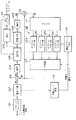
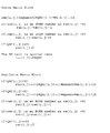
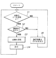
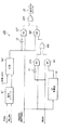
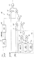
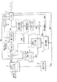
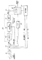
MPEG方式に基づいた動画像信号圧縮装置の構成例を図1に示す。この図1に示す動画像信号圧縮装置では、ディジタル動画像信号がブロック化回路101に入力され、例えばNTSC方式などの標準ビデオフォーマットからブロックフォーマットに変換されて、ブロック化動画像信号が生成される。ここで、動画像信号の各画像は、空間軸方向、すなわち水平方向及び垂直方向に16×16画素のマクロブロックに分割される。マクロブロックはさらに8×8画素のブロックに細分割される。
【0013】
図1に示す動画像信号圧縮装置は、画像を構成するブロック全てが処理されるまで、動画像信号の各画像をブロック単位で圧縮する。つぎに、この動画像信号圧縮装置は、動画像信号の別の画像を処理するが、この別の画像は、動画像を構成する一連の画像における次の画像であってもよく、なくてもよい。以下に、図1に示す動画像信号圧縮装置における1つの画像内の画素の1ブロックの圧縮について説明する。圧縮される画素のブロックは現画像ブロックである。ブロック化動画像信号は動き予測器102に供給される。動き予測器102は、現画像ブロックS1を含む現画像をブロック単位で差分ブロック算出回路103に供給する。
【0014】
差分ブロック算出回路103は、動き予測器102から現画像ブロックS1を受信するときに、動き予測器102からの現画像ブロックS1に対応するマッチングブロックS2を受信する。このマッチングブロックS2は、ピクチャメモリ群112に記憶された再生画像から予測器113によって得られる。差分ブロック算出回路103は、現画像ブロックS1と、これに対応するマッチングブロックS2との画素単位の差分をとる。得られる差分ブロックS3は直交変換回路104に供給される。
【0015】
直交変換回路104は、通常DCT回路であり、差分ブロックS3を直交変換し、得られる変換係数のブロックを量子化器105に供給する。量子化器105は、変換係数のブロックを量子化して量子化変換係数のブロックを生成する。可変長符号化器106は、量子化器105からの量子化変換係数のブロックに、ハフマン符号化、ランレングス符号化等の可変長符号化を施す。そして、得られる符号化変換係数のブロックは出力バッファ107を介して、例えばディジタル伝送路に出力される。
【0016】
出力バッファ107に記憶されたビット数を示す制御信号は、量子化器105にフィードバックされる。量子化器105は、この制御信号に応じて量子化ステップサイズを調整して、そのオーバフローやアンダフローを防止する。
【0017】
また、量子化変換係数のブロックは、量子化器105から逆量子化器108に送られる。逆量子化器108は、この動画像信号圧縮装置での予測符号化の際に用いられる再生画像を量子化変換係数から生成する局部復号化器の一部である。逆量子化器108は、量子化器105による量子化処理と相補的な処理を行うことにより、量子化変換係数のブロックを逆量子化する。得られる変換係数のブロックは、逆直交変換回路109に送られ、そこで直交変換回路104による直交変換処理と相補的な処理を行うことによって、逆直交変換される。得られる再生差分ブロックS4は加算器110に供給される。
【0018】
また、この加算器110は、ピクチャメモリ群112のうちの予測器113によって選択された1つのピクチャメモリから、現画像ブロックS1に対応したマッチングブロックS2が供給されている。加算器110は、逆直交変換回路109からの再生差分ブロックS4と、ピクチャメモリ群112からのマッチングブロックS2との画素単位の加算を行い、再生画像ブロックS5を生成する。再生画像ブロックS5は、セレクタ111により選択されたピクチャメモリ112A〜112Dのうち何れか1つに供給されて、記憶される。
【0019】
再生画像ブロックS5は、選択されたピクチャメモリに記憶され、そのピクチャメモリ内の再生される画像の(現画像ブロックに対応する)1ブロックをブロック単位で形成する。その後、再生画像は、動画像信号の他の画像を圧縮する予測符号化のためのマッチングブロックS2を得るのに用いられる。
【0020】
動き予測器102は、現画像のマクロブロック毎に、現画像のマクロブロックと、記憶されている動画像信号の他の画像の異なるマクロブロックとの動きベクトルを決定する。また、動き予測器102は、現画像の各マクロブロック内の画素と、他の画像の異なるマクロブロック内の画素との差分の絶対値和(絶対値差分和)を生成する。各絶対値差分和は、現画像の各マクロブロックと、他の画像のマクロブロックとのマッチングの度合を示す。動き予測器102は、各動きベクトルとそれに対応する絶対値差分和を予測モード決定回路115に供給する。
【0021】
予測モード決定回路115は、動き予測器102からのデータを用いて、1以上の他の再生画像に基づいて現画像を予測符号化するのに用いられる予測モードを決定する。現画像は、以下の予測モードの何れか1つを用いて予測符号化することができる。
【0022】
(1)他の画像を参照せず画像自体で圧縮される画像内モード。このように符号化された画像はIピクチャと称せられる。
【0023】
(2)動画像において時間的に先行する再生画像を参照して予測を行う前方予測モード。このように符号化された画像はPピクチャと称せられる。
【0024】
(3)動画像において時間的に先行する再生画像と動画像において時間的に後行する再生画像を参照して、あるいは、先行する再生画像と後行する再生画像の画素単位の線形演算(例えば、平均値計算)を行うことにより、ブロック単位の予測を行う両方向予測モード。このように符号化された画像はBピクチャと称せられる。
【0025】
すなわち、Iピクチャは、画像内で画像内符号化が完結する画像である。Pピクチャは、動画像において時間的に前にある再生Iピクチャ又はPピクチャより予測される。Bピクチャは、時間的に前又は後にある再生Iピクチャ又はPピクチャを用いてブロック単位で予測されるか、あるいは、動画像において時間的に前にある再生Iピクチャ又はPピクチャと時間的に後にある再生Iピクチャ又はPピクチャから線形演算によって得られるブロックを用いて予測される。
【0026】
そして、予測モード決定回路115は、予測モード信号PMとそれに対応する動きベクトルを予測器113及び読出アドレス発生器114に供給する。読出アドレス発生器114は、動きベクトルに応じて、ピクチャメモリ群112に読出アドレスを供給し、ピクチャメモリ112A乃至112Dから記憶されている再生画像のブロックを読み出させる。再生画像の読出ブロックの位置は、動きベクトルにより指定される。予測器113は、予測モード決定回路115からの予測モード信号PMに基づいて、ピクチャメモリ112A乃至112Dから読み出されたブロックのうちの1つを選択する。選択された読出ブロックは、現画像ブロックS1に対するマッチングブロックS2である。現画像ブロックがBピクチャの一部である場合、予測器113は、ピクチャメモリ112A乃至112Dからの読出ブロックに対して線形演算を行い、必要なマッチングブロックS2を生成する。予測器113は、マッチングブロックS2を差分ブロック算出回路103と加算器110に供給する。
【0027】
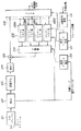
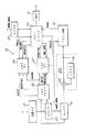
MPEG方式による動画像信号伸長装置の構成例を図2に示す。この動画像信号伸長装置では、動画像信号圧縮装置から直接、あるいは記録媒体から再生された圧縮動画像信号は、ビットストリームとして入力バッファ121に供給され、一時的に記憶される。圧縮動画像信号は、符号化変換ブロック(現画像ブロックを表す符号化変換係数のブロックを含む)、及び各ブロックの予測モード情報、量子化ステップサイズ情報、動きベクトルからなる。
【0028】
圧縮動画像信号は、入力バッファ121から1画像毎に読み出されて、逆可変長符号化器(IVLC)122に供給される。この逆可変長符号化器122は、圧縮動画像信号に逆可変長符号化を施して、圧縮動画像信号を量子化変換係数のブロック、及び各ブロックの予測モード情報、量子化ステップサイズ情報、動きベクトルからなる成分に分離する。
【0029】
符号化変換係数の各ブロックは、逆量子化器123に供給され、この逆量子化器123は、ブロックの量子化ステップサイズを用いて量子化変換係数のブロックを逆量子化し、変換係数のブロックを生成する。逆直交変換回路124は、変換係数のブロックに逆直交変換処理、通常IDCT処理を施して、再生差分ブロックを生成する。逆量子化器123と逆直交変換回路124はそれぞれ、図1に示す動画像信号圧縮装置の量子化器105と直交変換回路104による処理と相補的な処理を行う。
【0030】
読出アドレス発生器130は、逆可変長符号化器122から供給される現画像ブロックの動きベクトルに応じて、ピクチャメモリ128A乃至128Dに読出アドレスを供給する。各ピクチャメモリ128A乃至128Dは、読出アドレスに基づいて、記憶されている再生画像のブロックを読み出す。予測器129は、予測モード信号PMに応じて、ピクチャメモリ128A乃至128Dからの読出ブロックの何れか1つを選択する。選択された読出ブロックは、現画像ブロックを再生するためのマッチングブロックである。現画像ブロックがBピクチャとして符号化された画像の一部をなす場合、予測器129は、ピクチャメモリ112A乃至112Dからの読出ブロックに対して線形演算を行って、マッチングブロックを生成する。予測器129は、マッチングブロックを加算器125に供給する。
【0031】
加算器125は、逆直交変換回路124からの再生差分ブロックと、予測器129からのマッチングブロックとの画素単位の加算を行って、現画像の現画像ブロックを再生する。セレクタ126は、再生現画像ブロックをピクチャメモリ128A乃至128Dの何れか1に送って記憶させ、そこで現画像が再生される。再生現画像ブロックは、選択されたピクチャメモリ内の再生現画像の現画像ブロックの位置に記憶される。現画像の再生ブロック全てが、選択されたピクチャメモリ128A乃至128Dに記憶されると、再生現画像は、読出が可能となり、動画像における時間的に前又は後にある他の画像を再生するのに参照される。
【0032】
ピクチャメモリ128A乃至128Dに記憶されている再生画像は、表示アドレス発生器127が発生する読出アドレスに応じて、セレクタ126を介し、出力動画像信号として読み出される。この出力動画像信号は、スキャンコンバータ(図示せず)によりピクチャメモリ128A乃至128Dから、例えばNTSC等の所定のビデオ信号フォーマットのラスタフォーマットで読み出される。得られる出力動画像信号は、例えばCRT等のディスプレイに表示される。この例では、同期信号発生器131は、外部同期発生器にロックされ、周期的にフレーム同期信号を発生し、これを表示アドレス発生器127に供給している。表示アドレス発生器127は、このフレーム同期信号に同期して読出アドレスを発生する。
【0033】
直交変換回路、例えば上述した動画像信号圧縮装置や動画像信号伸長装置で用いられているDCT回路やIDCT回路等は、整数で表される画素値や変換係数に対して有限ビット数でそれぞれ演算を行う。その結果、これらの直交変換回路での直交変換では、ビット数の打ち切りが生じることがある。このため、実数を用いた直交変換の精度や、直交変換を行う回路構成が異なり、直交変換の結果が異なってしまう。これにより、動画像信号圧縮装置と動画像信号伸長装置間や共通の圧縮信号を伸長する動画像信号伸長装置間でミスマッチが生じる。
【0034】
例えば、動画像信号圧縮装置では、圧縮動画像信号を生成する過程において、動画像信号から得られる差分ブロックは直交変換され、得られる変換係数は、所定の処理である量子化が施される。そして、動画像信号伸長装置においては、逆直交変換回路の実数演算精度や回路構成が動画像信号圧縮装置のものに対応していない場合、動画像信号伸長装置の出力が、動画像信号圧縮装置の入力と異なる可能性がある。すなわち、動画像信号伸長装置の出力は、動画像信号伸長装置に用いられている回路の演算精度や構成に依存する。
【0035】
逆直交変換の演算精度や回路構成は、逆直交変換を行う装置によって異なる。例えば、変換係数のブロックを、2つの異なる回路構成の同種の逆直交変換回路を用いて逆変換すると、結果は異なることがある。このような結果の差異は、逆直交変換ミスマッチ誤差(ミスマッチ誤差)と呼ばれる。
【0036】
MEPG方式は、DCTやIDCTの演算精度を規定しているが、演算方法や回路構成については何も規定していない。これは、MEPG方式の規格が決定される以前に、DCTやIDCTを行う回路や方法が開発されたためである。
【0037】
MEPG方式においては、上述のように、動画像信号圧縮装置は、例えば動画像信号に対して画像間動き補償予測符号化を行う。ここで、動画像信号はブロックに分割され、現画像ブロックと、再生画像に動き補償を行うことにより得られるマッチングブロックとから差分ブロックが生成され、この差分ブロックがDCT処理により直交変換される。得られる変換係数は量子化され、量子化変換係数は可変長符号化が施され、そして、符号化変換係数は、予測モード情報、量子化ステップサイズ情報及び動きベクトルとともに組み込まれて、圧縮動画像信号が生成される。
【0038】
動画像信号伸長装置は、符号化変換係数に逆可変長符号化を施し、逆可変長符号化により得られる量子化変換係数に逆量子化を行い、そして、逆量子化により得られる変換係数にIDCT処理を施す。得られる再生差分ブロックは、動きベクトルに応じて再生画像に動き補償を施すことにより得られるマッチングブロックに加算される。これにより得られる再生画像ブロックは、動画像出力信号を出力するための再生画像のブロックとして記憶され、参照画像としても使用される。
【0039】
動画像信号圧縮装置は、予測符号化を行うための再生画像を量子化変換係数から再生する局部復号化器を内部に備える。この局部復号化器は、逆量子化器と逆直交変換回路を備える。
【0040】
動画像信号圧縮装置の局部復号化器のIDCT回路と動画像信号伸長装置のIDCT回路の構成が異なると、動画像信号圧縮装置の局部復号化器で得られる再生画像が、動画像信号伸長装置で得られる再生画像と異なることがある。こうしたIDCT処理の実行による差異は、MPEG規格に準拠した動画像信号圧縮装置により生成した圧縮動画像信号を光ディスクなどの記録媒体に記録して販売する場合に問題を生じる。この光ディスクから再生された圧縮動画像信号を他の製造者により製造、販売された動画像信号伸長装置で伸長すると、再生画像が元の画像と異なることがある。しかも、その差異は、実際に使用された動画像信号伸長装置に依存する場合がある。圧縮動画像信号が、地上又は衛星放送、電話システム、ISDNシステム、ケーブル又は光配信システム等の配信システムにより配信される場合、異なる動画像信号伸長装置間で上述のような非互換性が生じる虞がある。
【0041】
ミスマッチ誤差が特に問題となるのは、画像間予測符号化を行う場合である。画像間予測符号化は、フィールド間符号化やフレーム間符号化である。画像間予測符号化では、次第にこのミスマッチ誤差は累積されてしまい、再生画像に致命的な破綻を生じる可能性がある。
【0042】
MPEG方式による動画像信号圧縮においては、各ビデオシーケンスは、例えば8又は12画像を単位とする画像群(GOP:Group OfPictures)に分割されている。各画像は、上述したようにIピクチャ、Pピクチャ、Bピクチャに分類される。
【0043】
Bピクチャは動き予測の参照画像としては使用されない。したがって、Bピクチャで生じるミスマッチ誤差により他の画像に誤差が生じることはない。
【0044】
Pピクチャでミスマッチ誤差が生じると、ミスマッチ誤差を有する画像が、予測符号化を行うためにピクチャメモリに記憶されることとなる。したがって、画像間予測符号化を行うと、ピクチャメモリ内に記憶されたPピクチャの誤差が次第に大きくなり、予測符号化により得られるPピクチャやBピクチャにも及ぶ。この誤差は、誤差の無いIピクチャ又はPピクチャにより置換されるまで累積されていく。
【0045】
同様に、Iピクチャにミスマッチ誤差が発生した場合、ミスマッチ誤差のある再生画像が、予測符号化を行うためにピクチャメモリに記憶されることとなる。したがって、画像間予測符号化を行うと、ピクチャメモリ内に記憶されたIピクチャの誤差が、次第に大きくなり、予測符号化により得られるPピクチャやBピクチャにも及ぶ。この誤差は、誤差の無いIピクチャにより置換されるまで累積されていく。
【0046】
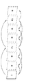
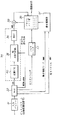
誤差の累積を図3に示す。図3において、Iピクチャを復号化する際に発生したミスマッチ誤差をEI、PピクチャP1を復号する際に発生したミスマッチ誤差をEP1とすると、再生されたPピクチャP1に含まれる誤差の値はEI+EP1となる。またPピクチャP2を復号する際に発生したミスマッチ誤差をEP2とすれば、再生されたPピクチャP2に含まれる誤差の値はEI+EP1+EP2となる。このように、個々のミスマッチ誤差は小さい値でも次第に累積していくと、大きな値の誤差となる。
【0047】
このとき動画像信号圧縮装置及び動画像信号伸長装置のMPEG復号化器で用いられるIDCT処理によって発生したミスマッチ誤差には、次の2つのものが存在する。
【0048】
(1)演算精度の不足に起因する誤差。
【0049】
(2)四捨五入の方法の違いに起因する誤差。
【0050】
演算精度はMPEGの規格で規定されているが、この規格は完全にミスマッチ誤差を発生させないほど十分ではなく、この規格を満たしているIDCT回路同士においても(1)のミスマッチ誤差が発生する可能性がある。
【0051】
IDCT処理の出力は整数であるから、IDCT処理の実数演算を行った後、演算結果を整数に丸めなければならない。一般的には、最も近い整数に丸められる。しかし、ここで問題となるのは演算結果が*.5(*は整数)という数となった場合である。MPEG方式では演算結果である*.5の丸め方法を規定していない。すなわち、あるIDCT回路ではこれを切り上げる処理を行うであろうし、またあるIDCT回路ではこれを切り捨てる処理を行う。また、演算結果の正負の符号により、丸め方法が異なる場合もある。この丸め方法の違いによって発生するミスマッチ誤差は、(2)のミスマッチ誤差である。
【0052】
ここで、(1)のミスマッチ誤差がランダムに発生するのに対し、(2)のミスマッチ誤差は体系的であるという点で、(1)のミスマッチ誤差は、(2)のミスマッチ誤差とは異なる。(1)のミスマッチ誤差はランダムに発生するので、正の誤差と負の誤差がほぼ同じ確立で発生する。したがって、長時間予測符号化を行った場合、(1)のミスマッチ誤差は平均化されていくと考えられる。
【0053】
一方、(2)のミスマッチ誤差は体系的であり、そのIDCT処理に固有のミスマッチ誤差であるので、一定して同一方向のミスマッチ誤差となる。したがって、長時間予測符号化を行うと、一方向に累積されていく。個々のミスマッチ誤差はわずか+1又は−1であるが、一方向に累積されていくと、その値は次第に大きな値となる。
【0054】
すなわち、(1)のミスマッチ誤差は、一時的には発生するものの、平均化されていくために、それほど大きな問題とはならない。一方、(2)のミスマッチ誤差は、一方向に累積するため、大きな問題となる。このため、累積する性質を有する(2)のミスマッチ誤差を防止する必要がある。
【0055】
MPEG1方式では、(2)のミスマッチ誤差を防止するために、IDCT処理を行う前に、処理を行うことが提案されている。この処理は、画像内符号化画像(イントラマクロブロックという。)におけるマクロブロックの(0,0)成分以外の全変換係数の成分を奇数とする処理である。例えば図4に示すように、(0,1)成分、(7,1)成分、(2,3)成分、(5,3)成分、(1,5)成分、(6,5)成分、(3,7)成分、(4,7)成分は何れも変換係数が568であり、偶数であるので、これを前処理により、例えば奇数である567とする。この前処理を行った変換係数に対してIDCT処理を行うと、常に端数が出なくなる。
【0056】
また、イントラマクロブロックのDC成分は、圧縮動画像信号から得られる画像において、視覚的に重要な信号であるので、その精度は8ビットに制限するのみにとどめておく。また、イントラマクロブロックのDC成分は、この重要成分の精度を低下させないために、奇数への変換は行わない。一方、画像間符号化を用いた符号化画像のマクロブロック(以下、ノンイントラマクロブロックという。)を変換することにより得られる変換係数は全て、イントラマクロブロックのDC成分以外の成分の変換係数と同様の処理を行い、変換係数を奇数のみに制限している。
【0057】
このようにIDCT処理の対象である変換係数の値を奇数に制限する処理を、奇数化処理と呼ぶ。
【0058】
このような奇数化処理を行うことにより、動画像信号圧縮装置と動画像信号伸長装置のIDCT処理が共通のルールで丸め処理を行い、画質の互換性を維持することができる。
【0059】
しかし、上述の奇数化処理を行っても、IDCT処理により*.5(*は整数)という結果が生じることがあるため、MPEG1の処理では、累積する性質を有する(2)のミスマッチ誤差が発生する。*.5という結果が生じる状況について、例えばMPEG方式における8×8の2次元IDCTを用いて以下に説明する。
【0060】
8×8の2次元IDCTは以下の式で表される。
【0061】
【数1】

上記の式において、F(u,v)は、2次元IDCTが施されるDCT係数を示す。式1において、IDCTの各出力値は実数、すなわち有理数や無理数である。*.5は有理数であるので、IDCTの出力値を無理数にすることにより、累積する性質を有するミスマッチ誤差の発生を防ぐことができる。また、出力値が有理数である場合、その出力値を*.5にすることができる。
【0063】
DCT係数であるF(0,0)、F(0,4)、F(4,0)、F(4,4)は、特殊なDCT係数である。これらのDCT係数の何れかが非零値をとる場合、IDCTの出力値は有理数となる。この場合のIDCTの出力値は式2により表される。
【0064】
【数2】
このように、特殊なDCT係数F(0,0)、F(0,4)、F(4,0)、F(4,4)の1つでも、4の倍数であって、8の倍数でない非零値をとる場合、出力値は*.5となる。
【0066】
上述の4つの特殊なDCT係数のみが非零値をとる係数である場合、IDCTの出力値は式3により表させる。
【0067】
【数3】
xとyの組合せが異なれば、式3中のf(x,y)は以下の値をとる。
【0069】
【数4】
このように、4つの特殊なDCT係数が、式4で表される値の何れかが4の倍数であり8の倍数でないという値をとれば、結果は*.5となる。
【0071】
すなわち、4つの特殊なDCT係数が非零値をとれば、IDCTの出力値が*.5となる可能性が高い。
【0072】
また、上述の4つのDCT係数以外にも、非零値をとるDCT係数を対称的に種々に組み合わせることにより、*.5という結果が得られる。例えば、
(1)DCT係数の組X(2n+1,2m+1)、X(2m+1,2n+1)が同一の非零値をとり、その値が4の倍数であり8の倍数でない場合。
【0073】
(2)DCT係数の組X(2n+1,2n+1)、X(8−2n−1,8−2n−1)が同一の非零値をとり、その値が4の倍数であり8の倍数でない場合。
【0074】
上記の表現において、X(i,j)は、8×8の2次元DCTの成分である変換係数である。
【0075】
実際の動画像信号がMPEG方式に準拠した動画像信号圧縮装置により圧縮される場合、非零DCT係数は上記のパターンで得られることが多く、これによりIDCT出力値は*.5となる。しかも、4つの特殊なDCT係数の値は、殆どの場合が非零である。
【0076】
上述したように、最も頻繁に*.5を発生させるDCT係数のパターンは、上述の4つのDCT係数が非零の値を有するときであるので、これらの場合に対策を施すことにより、ミスマッチ誤差の発生確率を下げることができる。
【0077】
MPEG1におけるイントラマクロブロック及びノンイントラマクロブロックの逆量子化方法を図5に示す。図5において、QAC(i,j)はDCT係数の(i,j)成分、Wi(i,j)は重み行列の(i,j)成分、mquantは量子化係数、rec(i,j)は逆量子化されたDCT係数の(i,j)成分を示す。逆量子化方法はC言語の構文で記述されている。C言語の構文については、Herbert Schildt, Using Turbo C, Osborne McGraw Hill (1988), p.83−87に記載されている。
【0078】
量子化された各DCT係数は逆量子化された後、IDCT処理が施されるが、MPEG1では、DCT係数が偶数であった場合、+1又は−1を加えてIDCT処理が施される値を全て奇数となるように処理を行う。この処理によると、例えば、4つのDCT係数のうちF(0,0)のみが非零の値を有する場合、F(0,0)が4の倍数でかつ8の倍数でないときにミスマッチ誤差を起こすので、DCT係数が全て奇数値を有するように処理を施して、IDCT変換すると、その結果は*.5とはなり得ない。同様に、4つの特殊なDCT係数の他のDCT係数F(0,4)、F(4,0)、F(4,4)のどれか1つのみが非零の値を有する場合、ミスマッチ誤差を発生させない。しかし、図4から分かるように、上述の4つのDCT係数の内、複数個の係数が非零の値を有する場合、あるいは上述の(1)、(2)のように対称的なDCT係数の組がある場合には、全DCT係数を奇数にしても、ミスマッチ誤差の発生を防ぐことができない。
【0079】
すなわち、MPEG1の奇数化処理では、非零の値を有するDCT係数が2個以上の場合、ミスマッチ誤差の発生を防ぐことができない。しかも、MPEG1では、偶数値を有する変換係数が存在してはならないので、MPEG1の奇数化処理は、量子化変換係数の分解能を劣化する。これにより、画質が低下し、高画質が求められる場合に問題となる。すなわち、累積する性質を有するミスマッチ誤差の防止方法であって、MPEG1の規格で提案されているものより優れた方法が切望されている。
【0080】
【発明が解決しようとする課題】
こうした従来技術の問題を解決するために、本発明の目的は、変換係数を逆直交変換する際に、累積する性質を有するミスマッチ誤差の発生を効果的に防ぐことができ、かつ、変換係数の分解能を劣化させない動画像信号圧縮装置及び方法、並びに圧縮動画像信号伸長装置を提供することである。
【0081】
また、本発明の目的は、ミスマッチ誤差の無い動画像信号圧縮装置及び方法、並びに圧縮動画像信号伸長装置を提供することである。
【0082】
【課題を解決するための手段】
本発明は、動画像信号圧縮装置を提供する。動画像信号は画像からなり、各画像はブロックに分割される。この動画像信号圧縮装置は、参照画像のマッチングブロックを用いて動画像信号のブロックを予測符号化して、差分ブロックを生成する予測符号化器を備える。差分ブロック符号化器は、予測符号化器からの差分ブロックを圧縮して、圧縮動画像信号を生成する。差分ブロック符号化器は、予測符号化器からの差分ブロックを直交変換して、変換係数ブロックを生成する直交変換回路と、直交変換回路からの変換係数ブロックを量子化して、圧縮信号ブロックを生成する量子化器とを備える。この圧縮信号ブロックから、圧縮動画像信号が得られる。
【0083】
また、この動画像信号圧縮装置は、差分ブロック符号化器からの圧縮信号ブロックを、この圧縮信号ブロックが逆直交変換される際の丸め誤差を発生させずに伸長して、再生差分ブロックを生成する局部復号化器を備える。この局部復号化器は、差分ブロック符号化器からの圧縮信号ブロックを逆量子化して、再生変換係数ブロックを生成する逆量子化器を備える。アキュムレータは、この逆量子化器からの各変換係数ブロックの再生変換係数の和を求め、この和のパリティがパリティ判定回路により判定される。和奇数化器は、パリティ判定回路により和のパリティが偶数であると判定されたときに動作し、ブロック内の再生変換係数のうちの1つのパリティを反転して、パリティ反転変換係数を生成する。このパリティ反転変換係数により、和は奇数になる。そして、和奇数化器は、パリティ反転変換係数を含む再生変換係数のブロックを逆直交変換回路に供給する。逆直交変換回路は、再生変換係数のブロックを逆直交変換して、再生差分ブロックを生成する。
【0084】
また、この動画像信号圧縮装置は、局部復号化器からの再生差分ブロックを予測復号化して、動画像信号のブロックに対応する画像ブロックを再生する予測復号化器を備える。また、この動画像信号圧縮装置は、予測復号化器からの再生画像ブロックを、動画像信号の他の画像を予測符号化するための参照画像として用いる再生画像ブロックとして記憶するピクチャメモリを備える。
【0085】
上述の動画像信号圧縮装置において、局部復号化器内のアキュムレータ、パリティ判定回路及び和奇数化器の代わりに、各再生変換係数の最下位ビットを判定する最下位ビット判定回路、各ブロック内の値が1の最下位ビットを有する再生変換係数をカウントするカウンタ、カウンタからのカウント値が偶数であるかを判定するカウント判定回路、及びこのカウント判定回路によりカウント値が偶数であると判定されたときに動作し、ブロック内の再生変換係数のうちの1つを変更して、カウント値を奇数にする変更変換係数を生成するカウント奇数化器を用いてもよい。
【0086】
また、本発明は、動画像出力信号を再生する圧縮動画像信号伸長装置を提供する。圧縮動画像信号は、動画像出力信号の画像をそれぞれ表す信号成分からなり、これらの信号成分は、可変長符号化された圧縮信号ブロックからなる。この圧縮動画像信号伸長装置は、可変長符号化された圧縮信号ブロックを逆可変長符号化して、圧縮信号ブロックを生成する逆可変長符号化器を備える。
【0087】
復号化器は、逆可変長符号化器からの圧縮信号ブロックを、この圧縮信号ブロックが逆直交変換されるときの丸め誤差を発生させずに伸長して、再生差分ブロックを生成する。この復号化器は、逆可変長符号化器からの各圧縮信号ブロックを逆量子化して再生変換係数ブロックを生成する逆量子化器を備える。アキュムレータは、この逆量子化器からの変換係数ブロック内の再生変換係数の和を求め、この和のパリティはパリティ判定回路により判定される。和奇数化器は、パリティ判定回路により和のパリティが偶数であると判定されときに動作し、ブロック内の再生変換係数のうちの1つのパリティを反転して、和のパリティを奇数にするパリティ反転変換係数を生成する。逆直交変換回路は、和奇数化器からパリティ反転変換係数を含む再生変換係数のブロックが供給され、再生差分ブロックを生成する。
【0088】
また、この圧縮動画像信号伸長装置は、復号化器からの再生差分ブロックを予測復号化して、画像ブロックを再生する予測復号化器と、予測復号化器からの再生画像ブロックを、再生画像のブロックとして記憶するピクチャメモリとを備える。また、この圧縮動画像信号伸長装置は、このピクチャメモリから動画像出力信号を読み出す回路を備える。
【0089】
上述の圧縮動画像信号伸長装置において、復号化器内のアキュムレータ、パリティ判定回路及び和奇数化器の代わりに、各再生変換係数の最下位ビットを判定する最下位ビット判定回路、各ブロックの値が1の最下位ビットを有する再生変換係数をカウントして、カウント値を出力するカウンタ、カウンタからのカウント値が偶数であるかを判定するカウント判定回路、及びこのカウント判定回路によりカウント値が偶数であると判定されたときに動作し、ブロック内の再生変換係数のうちの1つを変更して、カウント値を奇数にする変更変換係数を生成するカウント奇数化器を用いてもよい。
【0090】
さらに、本発明は、圧縮動画像信号を生成する動画像信号圧縮方法を提供する。この動画像信号圧縮方法においては、動画像信号ブロックに対して予測符号化及び直交変換処理が施され、変換係数ブロックが生成され、この変換係数ブロックから圧縮動画像信号が得られる。変換係数ブロックは、和が奇数化された後、逆直交変換及び予測復号化処理が施されて、動画像信号の他の画像を予測符号化するための参照画像として用いられる再生画像のブロックが生成される。
【0091】
また、本発明は、圧縮動画像信号を生成する動画像信号圧縮方法を提供する。この動画像信号圧縮方法においては、動画像信号の1画像のブロックと、参照画像としての再生画像信号のブロック間の動きが検出され、検出された動きに応じて、参照画像に動き補償が施され、参照画像のマッチングブロックが生成される。参照画像のマッチングブロックは、動画像信号のブロックを予測符号化するのに用いられ、差分ブロックが生成される。この差分ブロックは直交変換されて、変換係数ブロックが生成される。量子化及び可変長符号化を行うことにより、この変換係数ブロックから圧縮動画信号が生成される。逆直交変換処理における丸め誤差を防ぐために、各変換係数ブロックの和を奇数化した後、変換係数ブロックに逆直交変換処理が施され、再生差分ブロックが再生される。そして、再生差分ブロックが予測復号化され、動画像信号の他の画像を予測符号化するための参照画像として用いられる再生画像のブロックが生成される。
【0092】
【発明の実施の形態】
以下、本発明に係る動画像信号圧縮装置及び方法、並びに圧縮動画像信号伸長装置について、図面を参照しながら説明する。
【0093】
先ず、本発明の原理である累積する性質のミスマッチ誤差の防止について説明する。
【0094】
上述の式4を検討することにより、結果が(2n+1)/2(nは整数)である場合にミスマッチ誤差が発生することが分かる。
【0095】
式4は、以下のように要約できる。
【0096】
f(x,y) = 1/8 ACC
ここで、ACCは全係数の和である。最も多いミスマッチのパターンは、
f(x,y) = 1/8 ACC = (2n+1)/2 = 1/8(4*(2n+1))
である。
【0097】
これにより、ACCが奇数とされた場合、ミスマッチ誤差は発生しないことが分かる。
【0098】
したがって、本発明は、量子化DCT係数を逆量子化し、DCT係数の和を計算し、その後、IDCT処理を行う方式をとっている。DCT係数の和が偶数(すなわち、和のパリティが偶数)である場合、DCT係数のうちの1つのパリティを変更して、DCT係数の和を奇数(すなわち、和のパリティを奇数)にする。DCT係数の和を奇数化するには、1つのDCT係数のパリティを変更するだけで十分である。しかも、IDCTの出力値に最小の影響しか与えないDCT係数パリティであるから、変更することができる。つまり、本発明によれば、IDCT処理前にDCT係数の和のパリティをチェックすることにより、そして、和のパリティが偶数である場合、DCT係数の1つのパリティを変更してDCT係数の和を奇数化することにより、ミスマッチ誤差の発生を効果的に防ぐことができる。
【0099】
重要なことは、本発明によれば、DCT係数の和を奇数化するのに、1つのDCT係数のパリティを変更するだけで十分であるということである。MPEG1は、全DCT係数を奇数化し、その結果、IDCT処理が施されるDCT係数の分解能を劣化させてしまっている。これに対し、本発明によるミスマッチ誤差防止法は、IDCT回路の入出力値の精度を余り低下させずに、DCT係数の和を奇数化する。本発明の方法を動画像信号圧縮装置、圧縮動画像信号伸長装置、あるいは圧縮動画像信号伝送装置に適用すれば、画質の低下を最小限に抑えることができる。
【0100】
さらに、本発明の方法をMPEG方式に適用すれば、最小量子化ステップが2である従来技術に対し、最小量子化ステップを1にすることができる。
【0101】
この実施例は、本発明を、動き補償予測符号化と離散コサイン変換(DCT:Discrete Cosine Transform)を組み合わせたハイブリッド(hybrid)符号化方式に適用したものである。このハイブリッド符号化方式は、動画像の符号化規格のための国際的な委員会である、CCITT(国際電信電話諮問委員会)のH.261のISO−IEC/JTC1/SC2/WG11(通称MPEGという)で検討されており、蓄積メディア用の動画像信号の圧縮などにおいても採用されており、広く知られた方式である。WG11の報告には、ここで用いられる語の用語集が記載されている。
【0102】
動き補償予測符号化は、動画像信号の時間軸方向の相関を利用して動画像信号が有する冗長度を削減する方法である。既に復号化されている別の画像を参照画像として、現在の符号化対象である画像の信号を動き補償予測し、得られる動き補償予測誤差が動きベクトル、予測モードなどとともに圧縮信号に含まれる。これにより、現在の画像を表すのに必要な圧縮動画像信号の情報量を大幅に削減する。
【0103】
そして、上記動き補償予測誤差信号は、動画像を構成する各画像の空間軸方向の相関を利用する差分信号圧縮器により圧縮される。この差分信号圧縮器の一例としては、DCT回路などの直交変換回路と量子化器を組み合わせたものが代表的である。DCTは、直交変換の一種で、画像信号の有する画像内(フレーム内又はフィールド内)2次元相関性により、特定の周波数成分に信号電力を集中させる。この集中分布したDCT係数のみは、そのままあるいは追加圧縮後、圧縮信号に含まれる。これにより、現在の画像を表すのに必要な圧縮動画像信号の情報量をさらに削減する。
【0104】
画像間動き補償予測符号化は、動画像信号のフレーム間で行うこともできる。またインタレース画像信号のような場合には、フィールド間でも行うことができる。また、フレーム間符号化とフィールド間符号化を動画像信号の性質に応じて、適応的に切り換えることも可能である。
【0105】
第1の実施例
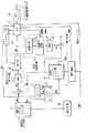
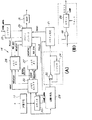
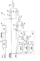
図6に、本発明を適用した動画像信号圧縮装置の具体的な構成を示す。図6に示す動画像信号圧縮装置においては、動画像信号が画像に分割され、画像単位で圧縮される。各画像は画像ブロックに分割され、ブロック単位で圧縮される。圧縮される画像ブロックは現画像ブロックと呼ばれる。現画像ブロックは現画像と呼ばれる画像のブロックである。
【0106】
動画像信号(通常、ビデオ信号)は、第1のピクチャメモリ群2に供給され、複数の画像が一旦記憶される。メモリコントローラ3は、第1のピクチャメモリ群2及び第2のピクチャメモリ群4の読出を制御する。また、メモリコントローラ3は、スライススタート信号SS及びマクロブロックスタート信号BSをスライス/マクロブロック・カウンタ5に供給する。メモリコントローラ3は、現在符号化の対象である第1のピクチャメモリ群2から読み出される画像のスライス又はマクロブロックに同期して、これらの信号を出力する。スライスは、画像の幅にわたるブロックの水平列である。
【0107】
動き予測器6は、第1のピクチャメモリ群2に記憶されている現画像ブロックと、過去の画像と未来の画像の各ブロックとのブロックマッチングを行うことによって、動き予測を行う。ブロックマッチングは、例えば16×16画素のブロックを用いて行う。現画像とブロックマッチされる過去の画像と未来の画像の各ブロックは、メモリコントローラ3から出力される動き予測参照画像指示信号に従って、第1のピクチャメモリ群2の中から選択される。そして、動き予測器6は、選択されたブロックと現画像ブロックとの差、すなわち動き予測誤差が最小となる第1のピクチャメモリ群2内の過去又は未来の画像中のブロック位置を、動きベクトルMVとして動き補償器7に供給する。
【0108】
動き補償器7は、動きベクトルMVに応じて、第2のピクチャメモリ群4に記憶されている各再生画像のブロックを潜在的なマッチングブロックとして読み出させる。これらの潜在的なマッチングブロックが読み出される再生画像の位置は、動きベクトルMVにより指定される。そして、第2のピクチャメモリ群4から読み出された潜在的なマッチングブロックのうちの1つが、メモリコントローラ3から出力される動き補償参照画像指示信号MAに従って、現画像ブロックに対するマッチングブロックとして選択される。第2のピクチャメモリ群4に記憶されている再生画像は、後述するように、差分ブロック符号化器9から出力される量子化DCT係数を局部復号化することにより再生された画像である。
【0109】
動き補償参照画像指示信号MAによりマッチングブロックが選択される再生画像は、現画像の予測モードによって異なる。前方向予測モードでは、マッチングブロックが過去の再生画像から選択される。両方行予測モードでは、マッチングブロックは、過去の再生画像又は未来の再生画像から選択されるか、あるいは過去の再生画像と未来の再生画像の各ブロックに対して線形演算(例えば、平均値計算)を行うことにより得ることができる。そして、現画像が画像内符号化モードで符号化される場合、すなわち画像が予測なしで符号化される場合、全画素値が零である零ブロックがマッチングブロックとして用いられる。第2のピクチャメモリ群4から読み出されるマッチングブロックは適応的であり、これにより、動画像信号の各ブロックについて最適なマッチングブロックの選択が行われる。
【0110】
動き補償器7は、まず、現画像ブロックと、異なる予測モードで得られる潜在的なマッチングブロックとの画素毎の差分の絶対値総和を計算することにより、各画像の予測モードを選択する。そして、この絶対値総和が最小である予測モードを選択する。動き補償器7は、選択された予測モードを示す動き補償モード信号MMを、後述する可変長符号化器17に供給する。また、動き補償器7は、第2のピクチャメモリ群4に、選択された予測モードのマッチングブロックS2を差分発生回路8に供給させる。
【0111】
この差分発生回路8は、第1のピクチャメモリ群2から読み出された動画像信号の現画像ブロックS1を受け取り、現画像ブロックS1とマッチングブロックS2との差分を画素単位で計算する。差分発生回路8は、得られる差分ブロックS3を差分ブロック符号化器9に供給する。差分ブロック符号化器9は、差分ブロックS3を圧縮して、量子化変換係数SCのブロックを生成する。量子化変換係数SCのブロックは、局部復号化器10に供給され、伸長されて再生差分ブロックS4が生成される。この動画像信号圧縮装置内の局部復号化器10は、後述する圧縮動画像信号伸長装置と類似した構成を有するが、詳細においては区別される。
【0112】
ここで、上記差分ブロック符号化器9、局部復号化器10について説明する。
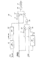
【0113】
差分ブロック号化器9は、図6に示すように、DCT回路11と量子化器12とを備える。DCT回路11は、差分発生回路8から供給される差分ブロックS3をDCT変換して、DCT係数を量子化器12に供給する。量子化器12は、DCT係数を量子化して、量子化DCT係数SCのブロックを出力する。
【0114】
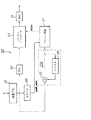
局部復号化器10は、図6に示すように、逆量子化器13と、和奇数化回路14と、IDCT回路15とを備えている。逆量子化器13は、量子化器12からの量子化DCT係数SCのブロックを量子化テーブルを用いて逆量子化する。和奇数化回路14は、DCT係数の和が奇数でないときに、DCT係数に対してパリティ反転を行う。これにより、和が奇数化されたDCT係数のブロックを逆直交変換する際には、ミスマッチ誤差が生じない。IDCT回路15は、和奇数化回路14からのDCT係数の和が奇数化されたブロックに対して逆離散コサイン変換(IDCT変換)を行って、再生差分ブロックS4を生成する。
【0115】
つぎに、量子化器12での具体的な量子化について説明する。量子化は8×8DCT係数からなるブロック単位で行われる。画像内符号化モードで圧縮される画像(Iピクチャ)の各ブロックはイントラマクロブロックと呼ばれる。画像間符号化モードで圧縮される各ブロックは、ノンイントラマクロブロックと呼ばれる。イントラマクロブロックが直交変換されると、(0,0)成分のDCT係数はDC係数となる。DC係数については、四捨五入により、8ビット精度での量子化の際にはDC係数を8で割り、9ビット精度での量子化の際にはDC係数を4で割り、10ビット精度での量子化の際にはDC係数を2で割り、11ビット精度での量子化の際にはDC係数を1で割ることにより、量子化される。すなわち、イントラマクロブロックのDC係数は、以下の式に従って量子化される。なお、以下の式はCプログラミング言語の構文で表されている。
QDC = dc // 8 (8 bits)
QDC = dc // 4 (9 bits)
QDC = dc // 2 (10 bits) (5)
QDC = dc // 1 (11 bits)
ここで、dcはDC係数、QDCは量子化されたDC係数をそれぞれ表す。
【0116】
イントラマクロブロックを直交変換することにより得られるDCT係数であって、DC成分以外の成分である各DCT係数(以下、AC係数という。)は、以下の式に従い、重み付け行列WiによってDCT係数ac(i,j)を重み付けして、量子化ファクタac (i,j)を求めることにより、量子化する。
ac (i,j) = (16*ac(i,j)) // Wi(i,j)(6)
重み付け行列Wiの係数を以下に示す。
【0117】
【数5】
ここで、p、qは固定の任意の整数であり、例えばp=3、q=4を用いる。mquantは量子化係数である。
【0119】
画像間符号化マクロブロック(ノンイントラマクロブロック)の直交変換により得られるDCT係数は、以下の式に従い、ノンイントラマクロブロックを変換して得られる全てのDCT係数を、重み付け行列Wnによって重み付けして、量子化ファクタac (i,j)を求めることにより、量子化する。
ac (i,j) = (16*ac(i,j)) // Wn(i,j)(9)
重み付け行列Wnの係数を以下に示す。
【0120】
可変長符号化器17は、DCT係数のブロックを量子化して得られる量子化DCT係数SCのブロックを可変長符号化する。可変長符号化器17は、各マクロブロックを構成する4つの輝度ブロックにおける量子化変換係数と、各イントラマクロブロックのDC係数との差分を求め、得られる差分値を可変長符号化テーブルを用いて可変長符号化する。これは、隣接する4つの輝度ブロックでは、相関が高く、DC係数が殆ど同じ値を有するからである。また、可変長符号化器17は、2つの色差ブロックの量子化係数の差分を求め、得られる差分値を可変長符号化テーブルを用いて可変長符号化する。なお、輝度用の可変長符号化テーブルと色差用の可変長符号化テーブルは異なるテーブルである。
【0121】
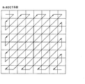
可変長符号化器17は、図7に示すように、(0,0)成分のDCT係数を先頭とするジグザグスキャンにより、量子化DCT係数を読み出して、量子化DCT係数ブロックを可変長符号化する。DCT変換により得られる非零DCT係数は、一般的に、(0,0)成分近傍に値が集中することから、量子化DCT係数SCのブロックはジグザグスキャンにより読み出される。すなわち、量子化DCT係数ブロックをジグザグスキャンによって読み出すことにより、各非零DCT係数間の連続した零DCT係数の個数(ラン)が増加し、可変長符号化の効率が向上する。
【0122】
可変長符号化器17は、量子化DCT係数をジグザグスキャンの順で読み出し、各非零DCT係数の値(レベル)と、それに先行する零DCT係数の個数(ラン)を求めて、量子化DCT係数ブロックを2次元可変長符号化する。符号化の後、ブロック内のDCT係数はランとレベルとの組合せにより表される。また、可変長符号化器17は、最後の非零DCT係数を示す2ビット符号EOBを付加する。また、可変長符号化器17は、またジグザグスキャンの順の最後の非零DCT係数のアドレスを、アドレス変換器(図示せず)に供給し、アドレス変換器は、ジグザグスキャンでのアドレスをラスタスキャンにおけるアドレスEOB_adrsに変換する。可変長符号化器17は、このアドレスEOB_adrsを和奇数化回路14に供給する。
【0123】
和奇数化回路14は、ラスタスキャンでのアドレスEOB_adrsを、例えば図8に示す後述のレジスタ25に記憶させる。
【0124】
つぎに、逆量子化器13について説明する。逆量子化器13は、差分ブロック符号化器9からの量子化DCT係数SCのブロックを受け取り、逆量子化して、DCT係数のブロックを生成する。具体的には、逆量子化器13は、イントラマクロブロックを直交変換して得られる量子化DC係数を、式12により逆量子化して、各DC係数を生成する。また、逆量子化器13は、ノンイントラマクロブロックを直交変換して得られるAC係数を、式13により逆量子化する。また、逆量子化器13は、ノンイントラマクロブロックを直交変換して得られるの全ての量子化係数を、式14により逆量子化する。
【0125】
和奇数化回路14は、アキュムレータ23Aと、パリティ判定回路21と、パリティインバータ28とを備えている。アキュムレータ23Aは、逆量子化器13からのDCT係数ブロックにおけるDCT係数の和を求める。パリティ判定回路21は、アキュムレータ23AからのDCT係数の和が偶数又は奇数の何れか、すなわち、DCT係数の和のパリティが偶数又は奇数の何れかを判定する。DCT係数の和のパリティが偶数であるとパリティ判定回路21が判定したときのみ、ブロック内のDCT係数の少なくとも1つのパリティを変更して、DCT係数の和のパリティを奇数にする。すなわち、DCT係数の和を奇数化する。これにより、和奇数化回路14からの和奇数化されたDCT係数のブロックがIDCT回路15により逆直交変換された場合に、ミスマッチ誤差の発生を防止する。
【0126】
カウンタ20は、逆量子化器13から供給されるDCT係数の数をカウントし、得られるカウント値coeff_adrsをパリティ判定回路21、メモリセレクタ22に供給する。
【0127】
アキュムレータ23Aは、加算器23とレジスタ24を備える。加算器23は、逆量子化器13から供給されるDCT係数のブロックの各DCT係数と、レジスタ24中に保存されているブロック内の先行するDCT係数の和とを加算する。各DCT係数ブロックの和が求められると、レジスタ24はリセットされる。得られるDCT係数の和は加算器23からレジスタ24とパリティ判定回路21に供給される。パリティ判定回路21がDCT係数の和のパリティが偶数又は奇数であると判定するのに適した結果を得るためには、アキュムレータ23Aは、ブロック内のDCT係数の最下位ビットのみの和を求めればよい。
【0128】
パリティ判定回路21は、カウンタ20から供給されるカウント値coeff_adrsに応じて、DCT係数ブロック内のDCT係数の和のパリティが奇数であるか偶数であるかを判定する。アキュムレータ23Aにブロック内の全てのDCT係数が供給されたとき、カウント値coeff_adrsは、アキュムレータ23Aがブロック内の全てのDCT係数の和を求めたことを示す。カウント値coeff_adrsに応じて、パリティ判定回路21は、アキュムレータ23AからのDCT係数の和のパリティが奇数であるか偶数であるかを判定する。例えば、8×8の2次元DCT変換の場合、カウント値coeff_adrsがブロック内の64個のDCT係数の和がアキュムレータ23Aに供給されたことを示すとき、パリティ判定回路21はアキュムレータ23AからのDCT係数の和のパリティが偶数であるか奇数であるかを判定する。
【0129】
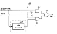
具体的には、例えばDCT係数が2進数で表現されていると、パリティ判定回路21は、アキュムレータ23Aから供給されるDCT係数の和の最下位ビット(LSB)を判定する。LSBが零のとき、和のパリティが偶数であることを示す。この場合、パリティ判定回路21は、パリティ反転を行うために処理要求信号REQ1をパリティインバータ28に出力する。この処理要求信号REQ1に応じて、パリティインバータ28は、DCT係数の少なくとも1つ(すなわち、奇数)のパリティを変更してDCT係数の和を奇数化する。一方、最下位ビットが1であるとき、和のパリティは奇数である。この場合、パリティ判定回路21は処理要求信号REQ1を出力せず、パリティインバータ28はブロック内の全てのDCT係数のパリティをそのままにしておく。
【0130】
具体的には、逆量子化器13からのDCT係数は、メモリセレクタ22を介して第1のメモリ26又は第2のメモリ27に記憶される。すなわち、メモリセレクタ22は、カウンタ20から供給されるカウント値coeff_adrsに基づいて動作する。例えばメモリセレクタ22は、第1のメモリ26に全てのDCT係数が記憶されたと判定したとき、第2のメモリ27に次のブロックのDCT係数が記憶されるようにメモリを指定する。このようにして、DCT係数の連続したブロックが交互に第1のメモリ26、第2のメモリ27に記憶される。ブロック内の全てのDCT係数が第1のメモリ26又は第2のメモリ27の何れかに記憶された場合、全てのDCT係数が記憶されたメモリはメモリフル信号FULL1又はメモリフル信号FULL2をパリティインバータ28に出力する。
【0131】
パリティインバータ28は、メモリフル信号FULL1又はメモリフル信号FULL2を受け取ると、そのメモリフル信号を発生したメモリにリードイネーブル信号RD_EN1又はリードイネーブル信号RD_EN2を供給する。これにより、DCT係数ブロックが、メモリフル信号を発生したメモリからパリティインバータ28に供給される。パリティインバータ28は、パリティ判定回路21からの処理要求信号REQ1の有無に基づいて、メモリから読み出されたDCT係数ブロックを処理する。パリティインバータ28は、処理要求信号REQ1を受け取ると、ブロック内のDCT係数のうちの1つ、例えばジグザグスキャンにおける最後の非零のDCT係数の最下位ビットを反転する。パリティインバータ28は、レジスタ25に記憶されているパリティ反転が可能なDCT係数のアドレスを用いて、パリティ反転が可能なDCT係数を識別する。例えば、図11は、パリティインバータ28の具体的な構成を示すブロック図である。比較器62には、最後の非零のDCT係数のアドレスEOB_adrsが供給される。したがって、パリティ反転が可能なDCT係数は、最後の非零のDCT係数となる。パリティインバータ28がパリティ反転が可能なDCT係数のパリティを反転すると、ブロック内の先頭から最後までの非零のDCT係数の和のパリティは奇数となる。パリティインバータ28は、LSBが反転されたDCT係数以外の全てのDCT係数を、LSBはそのままの状態で、IDCT回路15に供給する。また、このパリティインバータ28は、パリティ反転が可能なDCT係数を、パリティインバータ28が処理要求信号REQ1を受け取ったか否かでLSBが異なる状態で、IDCT回路15に供給する。
【0132】
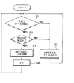
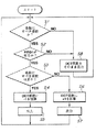
パリティインバータ28は、例えば図9に示すフローチャートに従って動作するコンピュータ又はディジタル信号処理器を備えてもよい。この例では、パリティ反転可能なDCT係数は最後の非零のDCT係数とする。ステップS1において、パリティインバータ28は、アドレスEOB_adrsに基づいて、そのDCT係数がLSB反転によりパリティ反転が可能であるかを判定し、該当する(YESの)ときはステップS2に進み、該当しない(NOの)ときは後述するステップS5に進む。
【0133】
ステップS2において、パリティインバータ28は、処理要求信号REQ1の有無を判定し、処理要求信号REQ1が有ることを示すYESのときはステップS3に進み、処理要求が無いときはステップS5に進む。
【0134】
ステップS3において、パリティインバータ28は、パリティ反転可能なDCT係数のLSBを反転してパリティを反転し、DCT係数の和のパリティを変更する。そして、ステップS4に進み、パリティ反転したDCT係数をIDCT回路15(図8)に供給する。その後、ステップS1に戻り、次のDCT係数ブロックを処理する。
【0135】
処理したDCT係数がパリティ反転可能なDCT係数でないとき、あるいはパリティ反転すべきDCT係数がパリティ反転されないとき、すなわち処理要求信号REQ1が受け取られていないときは、ステップS5に進む。ステップS5において、DCT係数はそのままIDCT回路15に供給される。その後、ステップS1に戻り、次のDCT係数を処理する。
【0136】
DCT係数が2の補数表現で表される場合、LSBも2の補数表現のLSBとなる。また、DCT係数が符号と絶対値に分けて表現される場合、そのLSBは絶対値のLSBとなる。
【0137】
ところで、和奇数化回路14の構成は、上述の図8に示す構成に限定されるものではなく、例えば図10Aに示すように、図8に示す和奇数化回路14において、LSB検出器29を付加し、加算器23の代わりに排他的論理和ゲート30を用いてもよい。なお、図8に示す回路の構成要素に対応する図10Aに示す回路の構成要素には、同じ指示符号を付して、説明は割愛する。
【0138】
図10Aにおいて、LSB検出器29は、DCT係数のブロック内の各DCT係数のLSBを検出する。排他的論理和ゲート30は、ブロック内の各DCT係数と、レジスタ24に記憶されいる処理済みのDCT係数のLSBの排他的論理和との排他的論理和演算を行う。排他的論理和ゲート30とレジスタ24は、各ブロックのDCT係数のLSBの排他的論理和を算出する。排他的論理和ゲート30とレジスタ24との組合せにより、値が1のLSBを有するDCT係数をカウントすることにもなる。そして、ブロック内の全てのDCT係数が受け取られたとき、排他的論理和ゲート30の出力の状態は、値が1のLSBを有するDCT係数のカウント値が偶数であるか奇数であるかを示す。そして、パリティ判定回路21は、値が1のLSBを有するDCT係数のカウント値が偶数である場合、処理要求信号REQ1を発生する。
【0139】
図10Bは、排他的論理和ゲート30とレジスタ24の代わりに用いることができる別の回路構成を示す。ここで、逆量子化器13から供給された各DCT係数のLSBは、LSB検出器29からANDゲート88に供給される。ANDゲート88は、値が1のLSBのみをカウンタ89に送る。カウンタ89は、DCT係数の各ブロックの初めにリセットされ、供給される値が1の各LSBをカウントする。カウンタ89からのカウント値COUNTのLSBは、パリティ判定回路21に供給される。各ブロックの終わりで、パリティ判定回路21は、カウンタ89からのカウント値COUNTのLSBのパリティを求める。カウント値COUNTのLSBのパリティが奇数(例えば、COUNTのLSBが1)である場合、ブロック内の値が1のLSBを有するDCT係数が奇数個有り、ブロック内のDCT係数の和のパリティが奇数であることを示す。一方、カウント値COUNTのLSBのパリティが偶数(例えば、COUNTのLSBが0)である場合、ブロック内の値が1のLSBを有するDCT係数が偶数個有り、ブロック内のDCT係数の和のパリティが偶数であることを示す。
【0140】
図8及び10に示す和奇数化回路14におけるパリティインバータ28の第1の実施例の具体的な構成を、図11を参照して説明する。パリティインバータ28は、読出カウンタ61、比較器62、LSBインバータ63、ANDゲート64、65、67、68、ORゲート66、69、インバータ71、72を備えている。
【0141】
そして、パリティインバータ28は以下のように動作する。読出カウンタ61が第1のメモリ26又は第2のメモリ27からメモリフル信号FULLを受け取ると、第1のメモリ26又は第2のメモリ27にリードイネーブル信号RD_ENを送る。このリードイネーブル信号RD_ENにより、記憶されたDCT係数ブロックのDCT係数は順次、信号線RDATAを介して第1のANDゲート67に供給される。
【0142】
また、メモリフル信号FULLにより、読出カウンタ61は、受け取ったDCT係数のカウントを開始するとともに、このDCT係数の数を示すカウント値を比較器62に供給する。比較器62は、カウント値とレジスタ25から供給されるアドレスを比較して、第1のANDゲート67に供給されているDCT係数がパリティ反転を行うDCT係数であるか、すなわちLSB反転を行うDCT係数であるかを判定をする。図11に示す例では、パリティ反転を行うDCT係数は、レジスタ25に記憶されたアドレスEOB_adrsにより認識された最後の非零のDCT係数である。比較器62は、カウント値がパリティ反転を行うDCT係数のアドレスに一致したとき、すなわちこの例ではアドレスEOB_adrsに一致したとき、パリティ反転を行うDCT係数と判定して、その出力を0から1に変更する。
【0143】
比較器62の出力は、直接第2のANDゲート68に供給されるとともに、インバータ72を介して第1のANDゲート67に供給される。そして、カウント値がアドレスEOB_adrsと一致しないとき、第1のANDゲート67が開き、第2のANDゲート68が閉じる。これにより、DCT係数が、そのまま第1のANDゲート67とORゲート69を介してIDCT回路15に出力される。
【0144】
一方、パリティインバータ28に供給されたDCT係数がパリティ反転を行うDCT係数であり、カウント値がパリティ反転を行うDCT係数のアドレス、例えばEOB_adrsと一致したときは、比較器62の出力が上述のように変化する。これにより、第1のANDゲート67が閉じ、第2のANDゲート68が開き、ORゲート66を介して供給されるLSB反転されたDCT係数が、第2のANDゲート68とORゲート69を介してIDCT回路15に出力される。
【0145】
LSB反転されたDCT係数は、DCT係数を信号線RDATAを介して第3のANDゲート64とLSBインバータ63に供給することにより、処理要求信号REQ1に応じて、選択的にIDCT回路15に供給される。処理要求信号REQ1は、パリティ判定回路21から直接第4のANDゲート65に供給されるとともに、インバータ71を介して第3のANDゲート64に供給されている。LSBインバータ63は、信号線RDATAを介して供給される各DCT係数のLSBを反転し、得られるLSB反転されたDCT係数を第4のANDゲート65に供給する。
【0146】
そして、処理要求信号REQ1が無いとき、すなわち処理要求信号REQ1が0のとき、パリティ反転を行うDCT係数は、LSB反転されずにIDCT回路15に送られる。具体的には、この0の処理要求信号REQ1により、第3のANDゲート64が開き、第4のANDゲート65が閉じ、LSBが反転されない、すなわちパリティを変更しないDCT係数は、信号線RDATAから第3のANDゲート64、ORゲート66、第2のANDゲート68及びORゲート69を介してIDCT回路15に供給される。
【0147】
一方、処理要求信号REQ1が有るとき、すなわち処理要求信号REQ1が1のとき、パリティ反転を行うDCT係数は、LSB反転されてIDCT回路15に供給され、DCT係数の和のパリティを変更する。具体的には、この1の処理要求信号REQ1により、第3のANDゲート64が閉じ、第4のANDゲート65が開き、LSB反転されたパリティ反転を行うDCT係数が、LSBインバータ63から第4のANDゲート65、ORゲート66、第2のANDゲート68及びORゲート69を介してIDCT回路15に供給される。
【0148】
つぎに、このパリティインバータ28の第2の実施例について、図12を参照しながら説明する。このパリティインバータ28の第2の実施例は、処理要求信号REQ1が入力されると、パリティ反転を行うDCT係数に1を加算してDCT係数の和を奇数化するものである。
【0149】
パリティインバータ28の第2の実施例として、図12に示すフローチャートに従って動作するコンピュータ又はディジタル信号処理器を用いてもよい。図12に示すフローチャートは、ステップS3での処理を除けば、図9に示すフローチャートと同じである。ステップS3において、パリティインバータ28の第2の実施例では、パリティ反転を行うDCT係数のLSBを反転する代わりに、パリティ反転を行うDCT係数に1を加算してDCT係数の和を奇数化する。パリティ反転を行うDCT係数は、例えば、ブロック内の最後の非零のDCT係数であるか、最高周波数成分のDCT係数であってもよい。
【0150】
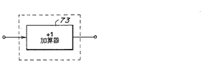
具体的には、パリティインバータ28の第2の実施例の具体的な回路構成は、パリティ反転を行うDCT係数に1を加算してブロック内のDCT係数の和を奇数化するものであり、その具体的な回路について、図13を参照して説明する。図13に示すパリティインバータ28の第2の実施例は、図11に示すパリティインバータ28の第1の実施例と略同じ構成を有する。図11に示す回路の構成要素に対応する図13に示す回路の構成要素は、同一符号を付して、説明は割愛する。
【0151】
図13に示すパリティインバータ28は、図11に示すLSBインバータ63の代わりに+1加算器73を備える。この+1加算器73は、第1のメモリ26又は第2のメモリ27から読み出され、信号線RDATAを介して供給された各DCT係数に1を加算する。1が加算されたDCT係数のうちの1つが、処理要求信号REQ1に応じて選択され、DCT係数の和を奇数化する。
【0152】
図13に示すパリティインバータ28の処理は、+1加算器73が信号線RDATAを介して得られる各DCT係数に1を加算すること以外は、図11に示す回路の処理と同じである。また、処理要求信号REQ1が有り、パリティ反転を行うDCT係数が検出されると、1が加算されたDCT係数は、+1加算器73から第4のANDゲート65、ORゲート66、第2のANDゲート68及びORゲート69を介してIDCT回路15に供給される。
【0153】
以下、パリティインバータ28の第3の実施例について、図14及び15を参照して説明する。
【0154】
このパリティインバータ28の第3の実施例は、処理要求信号REQ1が入力されると、パリティ反転を行うDCT係数の代わりに、DCT係数の符号が正であるとき1を引算し、負であるとき1を加算してパリティ反転されたDCT係数を用い、ブロック内のDCT係数の和を奇数化する。この処理により、パリティ反転を行うDCT係数のパリティを反転するのみならず、このDCT係数の大きさを削減する。すなわち、パリティ反転を行うDCT係数を0に近づける。パリティ反転を行うDCT係数に施す処理は以下の式により求められる。
rec > 0 ならば、
rec = rec − 1
rec < 0 ならば、
rec = rec + 1 (15)
ここで、recはパリティ反転を行うDCT係数を示す。
【0155】
パリティインバータ28の第3の実施例では、例えば図14に示すフローチャートに従って動作するコンピュータ又はディジタル信号処理器を用いてもよい。ステップS1において、パリティインバータ28は、アドレスEOB_adrsに基づいて、そのDCT係数がパリティ反転すべきDCT係数かを判定する。例えば、パリティインバータ28は、DCT係数が最後の非零DCT係数であるか否かを判定する。結果がYESであり、DCT係数がパリティ反転を行うDCT係数であるときはステップS2に進む。これに該当せず、DCT係数がパリティ反転を行わないDCT係数であるときはステップS8に進む。
【0156】
ステップS2において、パリティインバータ28は、処理要求信号REQ1の有無を判定し、処理要求信号REQ1が有る(YESの)ときはステップS3に進み、無いときはステップS8に進む。ステップS2におけるYESの結果は、ステップS1でYESとなるときのみ得られるので、DCT係数がパリティ反転を行うDCT係数であることを示す。
【0157】
ステップS3において、パリティインバータ28は、パリティ反転を行うDCT係数の極性を判定する。結果が、正であることを示すYESのときはステップS4に進み、0又は負のときはステップS6に進む。
【0158】
ステップS4において、パリティインバータ28は、パリティ反転を行うDCT係数から1を減算(−1を加算)した後、ステップS5に進み、パリティ反転したDCT係数をIDCT回路15(図10A)に出力する。その後、ステップS1に戻り、次のDCT係数を処理する。
【0159】
一方、ステップS6において、パリティインバータ28は、パリティ反転を行うDCT係数に1を加算した後、ステップS7に進み、パリティ反転したDCT係数をIDCT回路15に出力する。その後、ステップS1に戻り、次のDCT係数を処理する。
【0160】
DCT係数がパリティ反転すべきものでないとき、又はパリティ反転すべきDCT係数がパリティ反転されないとき、すなわち処理要求信号REQ1が無いときは、ステップS8に進む。ステップS8では、DCT係数はそのままIDCT回路15に供給される。その後、ステップS1に戻り、次のDCT係数を処理する。
【0161】
図15に、パリティ反転を行いDCT係数の大きさを削減する、すなわちDCT係数を0に近づけるパリティインバータ28の第3の実施例の回路構成についての具体例を示す。
【0162】
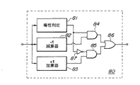
図15に示すパリティインバータ28は、図11に示すパリティインバータ28と略同じ構成を有する。図11に示す回路の構成要素に対応する図15に示す回路構成要素には、同一の指示符号を付し、説明は割愛する。図15に示すパリティインバータ28は、LSBインバータ63に代えて規模削減回路80を備える点で、図11のパリティインバータ28と異なる。
【0163】
そして、この規模削減回路80において、信号線RDATAを介して第1のメモリ26又は第2のメモリ27から供給された各DCT係数の極性が判定される。この規模削減回路80は、DCT係数の極性が正のときはDCT係数から1を減算し、0又は負のときは1を加算する。図15に示すパリティインバータ28は、規模削減回路80からのパリティ反転されたDCT係数を選択し、パリティ反転を行うDCT係数の代わりに、大きさが削減されるとともに、パリティ反転されたDCT係数を用いることにより、ブロック内のDCT係数の和を奇数化する。
【0164】
規模削減回路80は、直接第5のANDゲート84を制御するとともに、インバータ87を介して第6のANDゲート85を制御する極性判定回路81を備えている。また、規模削減回路80は、信号線RDATA上のDCT係数から1を減算する−1減算器82と、1を加算する+1加算器83を備える。−1減算器82又は+1加算器83の出力が、極性判定回路81の出力に応じて第5のANDゲート84又は第6のANDゲート85により選択される。ANDゲート84、85の出力はORゲート86に送られ、大きさが削減され、選択されたDCT係数が第4のANDゲート65に供給される。ブロック内のDCT係数の和のパリティを反転する必要がある場合、第4のANDゲート65は、大きさが削減され、パリティ反転された規模削減回路80の出力を選択して、パリティ反転を行うDCT係数の代わりにIDCT回路15に供給する。
【0165】
極性判定回路81は、信号線RDATAを介して供給されるDCT係数SCのブロック内の各DCT係数の極性を判定し、その極性の正負により、出力を1又は0とする。極性判定回路81が、DCT係数の極性が正であると判定した場合、極性判定回路81の出力は第5のANDゲート84を開き、第6のANDゲート85を閉じる。これにより、−1減算器82の出力、すなわち1が減算されたDCT係数が、第5のANDゲート84及びORゲート86を介して第4のANDゲート65に供給される。
【0166】
一方、DCT係数の極性が負又は0であると判定したときは、極性判定回路81の出力により第5のANDゲート84が閉じ、第6のANDゲート85が開く。これにより、+1加算器83の出力、すなわち1が加算されたDCT係数が、第6のANDゲート85及びORゲート86を介して第4のANDゲート65に供給される。
【0167】
第4のANDゲート65は、処理要求信号REQ1に応じて、パリティ反転され、大きさが削減されたDCT係数を、規模削減回路80から第2のANDゲート68に供給する。比較器62が、信号線RDATA上のDCT係数をパリティ反転を行うDCT係数であると判定したとき、大きさが削減され、パリティ反転されたDCT係数が、図15に示すように、規模削減回路80からIDCT回路15(図10A)に送られる。一方、図15に示すパリティインバータ28の第3の実施例で処理要求信号REQ1が無い場合、パリティ反転を行うDCT係数はそのままIDCT回路15に送られる。
【0168】
DCT係数の和が奇数化すべきものであるとき、図15に示すパリティインバータ28の第3の実施例では、極性が正のとき1を減算してパリティ反転し、負のときには1を加算してパリティ反転したDCT係数が、IDCT回路15に供給される。この処理により、パリティを反転し、パリティ反転を行うDCT係数の大きさを削減して、DCT係数の和を奇数化する。
【0169】
以下、パリティインバータ28の第4の実施例について、図16及び17を参照して説明する。
【0170】
このパリティインバータ28の第4の実施例は、処理要求信号REQ1が入力されると、パリティ反転を行うDCT係数の代わりに、極性が正のとき1を加算し、負のとき1を減算してパリティ反転を行うDCT係数を用いて、DCT係数の和を奇数化している。この処理により、パリティ反転を行うDCT係数のパリティを反転するのみならず、このDCT係数の大きさを増大する。すなわち、パリティ反転するDCT係数を0からさらに反転する。このパリティ反転を行うDCT係数に施す処理は、以下の式により求められる。
rec > 0 ならば、
rec = rec + 1
rec < 0 ならば、
rec = rec − 1 (16)
ここで、recはパリティ反転を行うDCT係数を示す。
【0171】
パリティインバータ28の第4の実施例では、図16に示すフローチャートに従って動作するコンピュータ又はディジタル信号処理器を用いてもよい。ステップS1において、パリティインバータ28は、アドレスEOB_adrsに基づいて、そのDCT係数がパリティ反転すべきDCT係数かを判定する。例えば、パリティインバータ28は、DCT係数が最後の非零のDCT係数であるか否かを判定する。結果がYESであり、DCT係数がパリティ反転を行うDCT係数であるときはステップS2に進む。これに該当せず、DCT係数がパリティ反転を行わないDCT係数であるときはステップS8に進む。
【0172】
ステップS2において、パリティインバータ28は、処理要求信号REQ1の有無を判定し、処理要求信号REQ1が有る(YESの)ときはステップS3に進み、無いときはステップS8に進む。ステップS2におけるYESの結果は、ステップS1でYESとなるときのみ得られるので、DCT係数がパリティ反転を行うDCT係数であることを示す。
【0173】
ステップS3において、パリティインバータ28は、パリティ反転を行うDCT係数の極性を判定する。結果が、正であることを示すYESのときはステップS4に進み、0又は負のときはステップS6に進む。
【0174】
ステップS4において、パリティインバータ28は、パリティ反転を行うDCT係数に1を加算した後、ステップS5に進み、パリティ反転したDCT係数をIDCT回路15(図10A)に出力する。その後、ステップS1に戻り、次のDCT係数を処理する。
【0175】
一方、ステップS6において、パリティインバータ28は、パリティ反転を行うDCT係数から1を減算(−1を加算)した後、ステップS7に進み、パリティ反転したDCT係数をIDCT回路15に出力する。その後、ステップS1に戻り、次のDCT係数を処理する。
【0176】
DCT係数がパリティ反転すべきものでないとき、又はパリティ反転すべきDCT係数がパリティ反転されないとき、すなわち処理要求信号REQ1が無いときは、ステップS8に進む。ステップS8では、DCT係数はそのままIDCT回路15に供給される。その後、ステップS1に戻り、次のDCT係数を処理する。
【0177】
図17に、パリティ反転を行いDCT係数の大きさを増大する、すなわちDCT係数を0からさらに反転するパリティインバータ28の第4の実施例の回路構成について具体例を示す。
【0178】
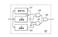
図17に示すパリティインバータ28は、図11に示すパリティインバータ28と略同じ構成を有する。図11に示す回路の構成要素に対応する図17に示す回路構成要素には、同一の指示符号を付し、説明は割愛する。図17に示すパリティインバータ28は、LSBインバータ63に代えて規模増大回路90を備える点で、図11のパリティインバータ28と異なる。
【0179】
そして、この規模増大回路90において、信号線RDATAを介して第1のメモリ26又は第2のメモリ27から供給された各DCT係数の極性が判定される。この規模増大回路90は、DCT係数の極性が正のときはDCT係数に1を加算し、0又は負のときは1を減算する。図17に示すパリティインバータ28は、規模増大回路90からのパリティ反転されたDCT係数を選択し、パリティ反転を行うDCT係数の代わりに、大きさが増大されたDCT係数を用いることにより、ブロック内のDCT係数の和を奇数化する。
【0180】
規模増大回路90は、直接第5のANDゲート94を制御するとともに、インバータ97を介して第6のANDゲート95を制御する極性判定回路91を備えている。また、規模増大回路90は、DCT係数に1を加算する+1加算器92と、1を減算する−1減算器93を備える。+1加算器92又は−1減算器93の何れかの出力が、極性判定回路91の出力に応じて第5のANDゲート94又は第6のANDゲート95により選択される。ANDゲート94、95の出力はORゲート96に送られ、大きさが増大され、選択されたDCT係数が第4のANDゲート65に供給される。ブロック内のDCT係数の和のパリティを反転する必要がある場合、第4のANDゲート65は、パリティ反転され、大きさが増大された規模増大回路90の出力を選択して、パリティ反転を行うDCT係数の代わりにIDCT回路15に供給する。
【0181】
極性判定回路91は、信号線RDATAを介して供給されるDCT係数のブロック内の各DCT係数の極性を判定し、その極性の正負により、出力を1又は0とする。極性判定回路91が、DCT係数の極性が正であると判定した場合、極性判定回路91の出力は、第5のANDゲート94を開き、第6のANDゲート95を閉じる。これにより、+1加算器92の出力、すなわち1が加算されたDCT係数が、第5のANDゲート94及びORゲート96を介して第4のANDゲート65に供給される。
【0182】
一方、DCT係数の極性が負又は0であると判定したときは、極性判定回路91の出力により第5のANDゲート94が閉じ、第6のANDゲート95が開く。これにより、−1減算器93の出力、すなわち1が減算されたDCT係数が、第6のANDゲート95及びORゲート96を介して第4のANDゲート65に供給される。
【0183】
第4のANDゲート65は、処理要求信号REQ1に応じて、パリティ反転され、大きさが増大されたDCT係数を、規模増大回路90から第2のANDゲート68に供給する。比較器62が、信号線RDATA上のDCT係数をパリティ反転を行うDCT係数であると判定したとき、DCT係数が、図11に示すように、規模増大回路90からIDCT回路15(図10A)に送られる。
【0184】
一方、図17に示すパリティインバータ28の第4の実施例において、処理要求信号REQ1が無い場合、パリティ反転を行うDCT係数はそのままIDCT回路15に送られる。
【0185】
DCT係数の和が奇数化すべきものであるとき、図17に示すパリティインバータ28の第4の実施例では、極性が正のとき1を加算し、負のときには1を減算してパリティ反転したDCT係数が、IDCT回路15に供給される。この処理により、パリティを反転し、パリティ反転を行うDCT係数の大きさを増大させて、DCT係数の和を奇数化する。
【0186】
図11、13、15、17に示すパリティインバータ28と、図9、12、14、16に示す演算処理は、ジグザグスキャンにより読み出される最後の非零のDCT係数以外のDCT係数のパリティを変更することにより、DCT係数の和を奇数化するように変更してもよい。例えば、8×8の2次元DCT変換において、DC成分のDCT係数、最高周波数成分である(7,7)成分のDCT係数、右上隅の(7,0)成分のDCT係数、又は左下隅の(0,7)成分のDCT係数としてもよい。特に最高周波数成分である(7,7)成分のDCT係数は画質に与える影響が小さいため、パリティ変更を行うDCT係数としては最良である。
【0187】
図11、13、15、17に示すパリティインバータ28において、比較器62に供給されるアドレスEOB_adrsに代えてDCT係数のアドレスを用いることにより、別のDCT係数を選択することも可能である。また、最高周波数成分のDCT係数のパリティが変更すべきものである場合、読出カウンタ61と比較器62は省略してもよく、パリティ変更を行うDCT係数として最高周波数成分のDCT係数を認識するのに、メモリフル信号FULLを用いてもよい。
【0188】
また、図6、8、10に示す和奇数化回路14は、ある特定のDCT係数、例えば(0,0)成分、(4,0)成分、(0,4)成分、(4,4)成分のDCT係数の和を求め、この和が奇数になるようにパリティ反転を行うこともできる。図18に、図8に示す和奇数化回路14の変更例を示す。ここでは、特定のDCT係数の和を求めて、パリティ反転が必要であるかを判定する。図8に示す和奇数化回路の構成要素に対応する図18に示す和奇数化回路の構成要素には同一の指示符号を付し、説明は割愛する。
【0189】
図18に示す和奇数化回路14は、逆量子化器13とアキュムレータ23Aとの間にセレクタ51を備える。セレクタ51は、カウンタ20から、逆量子化器13に供給されたブロック内のDCT係数の数を示すカウント値coeff_adrsを受け取る。
【0190】
そして、セレクタ51は、カウンタ20から供給されるカウント値coeff_adrsに基づいて、逆量子化器13から供給されている各DCT係数が特定のDCT係数であるか、及びアキュムレータ23Aにより求められる和に含まれるべきかを判定する。したがって、例えばセレクタ51は、カウント値coef_adrsが(0,0)成分、(4,0)成分、(0,4)成分、あるいは(4,4)成分に相当する値であるかを判定する。セレクタ51は、DCT係数が特定のDCT係数であると判定したとき、DCT係数をアキュムレータ23Aに供給する。これにより、図18に示すこの和奇数化回路14は、ブロック内の特定のDCT係数の和を求め、この和のパリティが偶数である場合、奇数となるように、少なくとも1つのDCT係数のパリティを変更する。図18に示す和奇数化回路14は、このパリティが処理されたDCT係数のブロックをIDCT回路15に供給する。
【0191】
図18に示す実施例は、図10Aに示すのと同様に変更することができ、その回路により特定のDCT係数のLSBの排他的論理和を求めるような構成にしてもよい。すなわち、図18に示す和奇数化回路を、加算器23を図10Aに示すLSB検出器29及び排他的論理和ゲート30に置き換えた構成とする。
【0192】
図6に戻り、DCT係数ブロック内のDCT係数は、上述のように、和奇数化回路14からIDCT回路15に供給される。和奇数化回路14からのDCT係数の和は奇数である。逆量子化器13からのDCT係数の和が偶数のとき、和奇数化回路14はDCT係数の少なくとも1つのパリティを変更して、IDCT回路15に供給するDCT係数の和を奇数化する。IDCT回路15は、ブロック内のDCT係数にIDCT処理を施し、再生差分ブロックS4を生成する。再生差分ブロックS4は加算器16に供給される。
【0193】
加算器16は、再生差分ブロックS4と第2のピクチャメモリ群4から供給されるマッチングブロックS2とを1画素毎に加算する。得られる再生画像ブロックS5は、第2のピクチャメモリ群4に供給され、メモリコントローラ3により指定されるピクチャメモリの1つに記憶されて、再生画像のブロックを再生する。
【0194】
可変長符号化器17は、差分ブロック符号化器9からの量子化されたDCT係数SCの各ブロックや、その動きベクトルMV、動き補償モードMM及び量子化テーブルのデータに対して、ハフマン符号化などの可変長符号化を行う。また、可変長符号化器17は、可変長符号化データを、MPEG規格のスタートコードや各層のヘッダ情報とともに組み合わせて、圧縮動画像信号を生成する。
【0195】
スライス/マクロブロック・カウンタ5は、第1のピクチャメモリ群2から読み出される画像の各スライス及び各マクロブロックのスタートに同期して、メモリコントローラ3から出力されるスライス・スタート信号SS及びマクロブロックスタート信号BSをカウントする。スライス/マクロブロック・カウンタ5は、そのカウント値が予め決められた値となったら、スタート信号S0を可変長符号化器17に出力する。
【0196】
このスタート信号S0を受けて、可変長符号化器17は、圧縮動画像信号を出力バッファ19に出力し、出力バッファ19は、圧縮動画像信号を一時的に記憶する。この圧縮動画像信号は、所定のビットレートでビットストリームとして出力バッファ19から読み出される。圧縮動画像信号のビットストリームは、伝送路を介して、あるいは光ディスク等の適当な記録媒体に記録することにより、相補型の圧縮動画像信号伸長装置に供給される。
【0197】
すなわち、記録媒体は、予測符号化されるとともに離散コサイン変換された動画像信号から得られる圧縮動画像信号が記録されている記録媒体である。予測符号化において参照画像として使用される再生画像の各ブロックは、圧縮動画像信号を構成する量子化DCT係数のブロックを逆量子化し、得られるDCT係数ブロックのDCT係数の和を奇数化して、和が奇数化されたDCT係数ブロックを逆DCT変換することにより再生される。
【0198】
ここで、本発明に係る伝送装置は、上述した本発明に係る動画像信号圧縮装置を備えている。
【0199】
ところで、動画像信号圧縮装置の差分ブロック符号化器9において和の奇数化を行う方が好適であると考えられる。和の奇数化により、圧縮動画像信号を構成する各量子化DCT係数ブロックのDCT係数の和は奇数となる。このように圧縮動画像信号を処理することにより、圧縮動画像信号伸長装置においてDCT係数の和を奇数化する必要がなくなると考えられる。しかし、このような構成では、DCT係数が動画像信号圧縮装置において量子化され、圧縮動画像信号伸長装置において逆量子化された後、圧縮動画像信号伸長装置のIDCT回路に入力されるDCT係数の和は奇数でなくなる。よって、和の奇数化処理は、圧縮動画像信号伸長装置のIDCT処理の前に行い、ミスマッチ誤差が発生しないようにしなければならない。
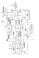
【0200】
つぎに、本発明を適用した圧縮動画像信号伸長装置について、図19を用いて説明する。図19において、圧縮動画像信号は、動画像圧縮装置から伝送路を介して、あるいは光ディスク等の適当な記録媒体から圧縮動画像信号を再生することにより、ビットストリームとして受信される。このビットストリームは入力バッファ31に供給され、一時的に記憶された後、読み出されて、画像毎に逆可変長符号化器(IVLC)32に供給される。逆可変長符号化器32は、MPEG符号のそれぞれの層のヘッダ情報を圧縮動画像信号から抽出し、このヘッダ情報から画像復号化制御情報PHをメモリコントローラ33に供給する。
【0201】
また、逆可変長符号化器32は、可変長符号化されたDCT係数のブロックを逆可変長符号化して、量子化DCT係数の現画像ブロックCbを含む量子化DCT係数のブロックを再生し、この量子化DCT係数ブロックCbを差分ブロック復号化器34に供給する。差分ブロック復号化器34は、量子化DCT係数ブロックCbを復号化して、再生差分ブロックBSを再生し、この再生差分ブロックBSを加算器39に供給する。
【0202】
また、逆可変長符号化器32は、圧縮動画像信号から動きベクトルMV及び量子化DCT係数ブロックCbの動き補償モードMMを抽出して、動き補償器37に供給する。この動き補償器37により、ピクチャメモリ群38から、再生差分ブロックBSに対応するマッチングブロックが読み出される。
【0203】
ピクチャメモリ群38は複数のピクチャメモリからなり、ピクチャメモリはそれぞれ既に再生された画像を記憶している。マッチングブロックは、ピクチャメモリの1つに記憶されている動きベクトルMVで指定されたアドレスに位置する再生画像のブロックである。このマッチングブロックが読み出される再生画像が記憶されているピクチャメモリは、メモリコントローラ33によってピクチャメモリ群38の中から指定される。
【0204】
上述のように、先行する再生画像からの予測、後行する再生画像からの予測、及び先行する再生画像と後行する再生画像に対する画素毎の線形演算を行うことにより得られるブロックからの予測により、画像が符号化される。また、画像を予測なしで符号化することもできる。この場合、ピクチャメモリ群38から供給されるマッチングブロックは、零ブロック、すなわち全画素値が零となっているブロックである。ピクチャメモリ群38から出力される動き補償されたマッチングブロックは、適応的なものとなっており、ブロック単位で最適なものが選択される。なお、ここでのブロックの大きさは16×16画素である。
【0205】
ピクチャメモリ群38から読み出された各マッチングブロックは、加算器39に供給される。加算器39は、差分ブロック復号化器34から供給される再生差分ブロックBSとピクチャメモリ群38から供給されるマッチングブロックとを1画素毎に加算する。この結果、再生画像ブロックが再生され、この再生画像ブロックは、メモリコントローラ33により指定されたピクチャメモリ群38の中のピクチャメモリに記憶される。加算器39から供給される再生画像ブロックは、先にピクチャメモリに記憶された再生画像に上書きされ、選択されたピクチャメモリに1つずつ記憶されて、新たな再生画像を形成する。
【0206】
ピクチャメモリ群38に記憶された再生画像は、メモリコントローラ33からの出力画像指示信号によって制御される順で読み出される。読み出された画像は、再生動画像信号として、ビデオモニターのような画像表示装置に供給される。画像表示装置は、この再生動画像信号に応じた動画像を表示する。
【0207】
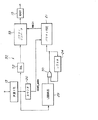
ここで、上記差分ブロック復号化器34について図19を参照して説明する。差分ブロック復号化器34は、逆量子化器40と、和奇数化回路35と、逆離散コサイン変換回路36とを備える。逆量子化器40は、逆可変長符号化器32から供給される量子化DCT係数ブロックCbを量子化テーブルを用いて逆量子化する。和奇数化回路35は、逆量子化器40からのDCT係数ブロックを受け取り、IDCT回路36でのIDCT処理におけるミスマッチ誤差の発生を防ぐ。IDCT回路36は、和奇数化回路35からの和が奇数化されたDCT係数ブロックをIDCT変換する。
【0208】
図20に、逆量子化器40の構成例を示す。この逆量子化器40は、主として、ラン/レベル復号化器41と、アドレスカウンタ47と、アドレス変換器48と、セレクタ49と、第1のブロックメモリ42と、第2のブロックメモリ43と、逆量子化回路(以下、IQ回路という。)46により構成される。
【0209】
ラン/レベル復号化器41は、逆可変長符号化器32から量子化DCT係数ブロックCbを受け取り、動画像信号圧縮装置の可変長符号化器17において量子化DCT係数に施されたラン/レベル符号化を復号化する。得られる量子化DCT係数ブロックは、ジグザグスキャンの順で、第1のブロックメモリ42又は第2のブロックメモリ43に供給される。第1のブロックメモリ42又は第2のブロックメモリ43は、量子化DCT係数ブロックを記憶する。
【0210】
アドレスカウンタ47とアドレス変換器48は、それぞれ、第1のブロックメモリ42と第2のブロックメモリ43の書込アドレスと読出アドレスとを出力する。量子化DCT係数ブロックは、第1のブロックメモリ42と第2のブロックメモリ43に対し交互に書き込まれ、読み出される。各量子化DCT係数ブロックは、アドレスカウンタ47から供給される書込アドレスに応じて、ジグザグスキャンの順でブロックメモリの1つに書き込まれ、アドレス変換器48から供給される読出アドレスに応じてラスタスキャンの順でブロックメモリから読み出される。書込と読出のアドレス順の違いにより、ブロック内の量子化DCT係数の順がジグザグスキャンからラスタスキャンに変換される。
【0211】
アドレスカウンタ47は、ジグザグスキャンの順で書込アドレスを発生する。アドレス変換器48は、アドレスカウンタ47からジグザグスキャンの順の書込アドレスを受け取り、これをアドレス変換テーブルを用いてラスタスキャンの順の読出アドレスに変換する。アドレスカウンタ47とアドレス変換器48が発生したアドレスは、セレクタ49により選択され、アドレスadrs1、adrs2として第1のブロックメモリ42及び第2のブロックメモリ43に供給される。ラン/レベル復号化器41からの量子化DCT係数ブロックが第1のブロックメモリ42又は第2のブロックメモリ43に書き込まれると、各アドレスadrs1、adrs2は、アドレスカウンタ47によりセレクタ49を介してジグザグスキャンの順で供給される。量子化DCT係数ブロックが第1のブロックメモリ42又は第2のブロックメモリ43からIQ回路46に読み出されると、各アドレスadrs1,adrs2は、アドレス変換器48からセレクタ49を介してラスタスキャンの順で供給される。
【0212】
第1のブロックメモリ42又は第2のブロックメモリ43に全ての量子化DCT係数が記憶されると、量子化DCT係数ブロックはラスタスキャンの順で読み出され、IQ回路46に供給される。IQ回路46は、ブロック内の量子化DCT係数を逆量子化し、得られるDCT係数ブロックを和奇数化回路35に供給する。このIQ回路46での逆量子化は、図6に示す動画像信号圧縮装置の局部復号化器を構成する逆量子化器13での逆量子化と同じである。
【0213】
和奇数化回路35は、逆量子化器40からのDCT係数ブロックのDCT係数の和のパリティが偶数であると判定したときは、DCT係数の和が奇数となるように、少なくとも1つのDCT係数に処理を施す。和奇数化回路35は、この和が奇数化されたDCT係数のブロックをIDCT回路36に供給する。なお、この和奇数化回路35での奇数化処理は、図6に示す動画像信号圧縮装置の局部復号化器を構成する和奇数化回路14での奇数化処理と同じである。
【0214】
IDCT回路36は、和が奇数化されたDCT係数ブロックをIDCT変換して、再生差分ブロックBSを再生し、この再生差分ブロックBSを加算器39に供給する。
【0215】
図20に示す逆量子化器40の具体的な動作を、図21A乃至21Iに示すタイミングチャートを用いて説明する。逆可変長符号化器32は、圧縮動画像信号から量子化されたDCT係数のブロックCbを取り出し、ラン/レベル復号化器41に対して量子化DCT係数ブロックを読み出すように指示するイベントイネーブル信号EV_EN(図21Aに示す)を発生する。量子化DCT係数ブロックのDCT係数は、ラン/レベル符号化されている。
【0216】
また、逆可変長符号化器32は、図21Bに示すように、イベント数信号EVENT_NOをラン/レベル復号化器41に出力する。イベント数信号EVENT_NOは、量子化DCT係数ブロックCb内のラン/レベルの組合せの数、すなわちランとレベルを示すデータの組合せの数を示すものである。
【0217】
ラン/レベル復号化器41は、このイベント数信号EVENT_NOを受け取ると、図21Cに示すように、各ラン/レベルの組合せについて読出要求信号RE_REQを逆可変長符号化器32に出力する。逆可変長符号化器32は、この読出要求信号RE_REQが入力されると、図21D、21Eに示すように、ラン/レベルの1組をラン/レベル復号化器41に出力し、これを受信した読出要求信号RE_REQの数だけ繰り返す。
【0218】
ラン/レベル復号化器41は、ラン/レベル符号化された量子化DCT係数を復号化し、図21Gに示すように、量子化されたDCT係数のブロックをWDATAとしてジグザグスキャンの順に第1のブロックメモリ42に供給する。これと同時に、図21Fに示すように、アドレスカウンタ47はラン/レベル復号化器41からの量子化DCT係数をカウントし、各量子化DCT係数の書込アドレスを示すアドレス信号adrs1を、セレクタ49を介してジグザグスキャンの順で第1のブロックメモリ42に供給する。
【0219】
そして、ラン/レベル復号化器41は、最後の非零のDCT係数を受信したことを示す符号EOBを逆可変長符号器32から受け取ると、符号EOBに対応する量子化DCT係数を設定し、すなわち符号EOB以降のDCT係数データは全て0として、この0のDCT係数データを第1のブロックメモリ42に供給する。
【0220】
また、ラン/レベル復号化器41は、符号EOBを受け取ると、図21Hに示すように、信号EOB_ENを位置(POS)レジスタ44、45に出力する。この信号EOB_ENは、符号EOBが受け取られたことをPOSレジスタ44、45に示すためのものである。POSレジスタ44、45は、第1と第2のブロックメモリ42、43に供給された各量子化DCT係数のアドレスを、アドレスカウンタ47からアドレス変換器48を介して受け取る。ラン/レベル復号化器41が符号EOBを受け取ると、アドレスカウンタ47により出力されるアドレスは最後の非零のDCT係数のアドレスとなる。信号EOB_ENにより、アドレス変換器48によりラスタスキャンアドレスに変換された最後の非零のDCT係数のアドレスEOB_POSは、量子化DCT係数ブロックが書き込まれているブロックメモリのPOSレジスタに書き込まれる。このようにして、POSレジスタ44、45の何れかが量子化DCT係数ブロックの最後の非零のDCT係数のアドレスを記憶する。
【0221】
ラン/レベル復号化器41が量子化DCT係数ブロックを全て第1のブロックメモリ42又は第2のブロックメモリ43に供給すると、アドレスカウンタ47は、バンク切換信号BANKを第1のブロックメモリ42と第2のブロックメモリ43に供給する。バンク切換信号BANKは、ブロックメモリのモードを切り換えて、書込モードであった第1のブロックメモリ42が読出モードに、第2のブロックメモリ43が書込モードに切り換えられる。したがって、ラン/レベル復号化器41が次の量子化DCT係数ブロックの復号化を開始すると、得られる量子化DCT係数は第2のブロックメモリ43に書き込まれることになる。また、バンク切換信号BANKはセレクタ49を切り換えて、書込モードでブロックメモリに供給されていたアドレスをアドレスカウンタ47からのジグザグスキャンの順のアドレスとし、読出モードでブロックメモリに供給されていたアドレスをアドレス変換器48からのラスタスキャンの順のアドレスとする。
【0222】
また、ラン/レベル復号化器41が量子化DCT係数ブロックを全て第1のブロックメモリ42に供給すると、第1のブロックメモリ42はメモリフル信号FULL1をIQ回路46に出力する。メモリフル信号FULL1は、全ての量子化DCT係数が記憶されたことを示すものである。IQ回路46は、メモリフル信号FULL1を受けとると、読出要求信号RD_EN1を第1のブロックメモリ42に送る。この読出要求信号RD_EN1により、第1のブロックメモリ42は、記憶している量子化DCT係数を、アドレス変換器48からセレクタ49を介してラスタスキャンの順で供給されるアドレスadrs1に応じて、読み出す。したがって、ブロック内の量子化DCT係数は第1のブロックメモリ42から読み出される。各アドレスに応じて読み出された量子化DCT係数はIQ回路46に供給される。ブロック内の量子化DCT係数が第1のブロックメモリ42から読み出されるのと同時に、次のブロックの量子化DCT係数が、アドレスカウンタ47からのアドレスに応じてジグザグスキャンの順で第2のブロックメモリ43に書き込まれる。
【0223】
IQ回路46は、図6に示す動画像信号圧縮装置の逆量子化器13と同様に、ブロックの量子化DCT係数を逆量子化して、得られるDCT係数を和奇数化回路35に供給する。
【0224】
1つのブロック内のDCT係数の和のパリティが偶数のとき、和奇数化回路35は、上述の動画像信号圧縮装置の和奇数化回路14と同様に、DCT係数の少なくとも1つを処理して、DCT係数の和を奇数化し、和が奇数化されたDCT係数のブロックをIDCT回路36に供給する。
【0225】
例えば、和奇数化回路35は、POSレジスタ44、45を参照し、ジグザグスキャン順での最後の非零のDCT係数かどうかの判定を行い、最後の非零のDCT係数のパリティを処理してブロックのDCT係数の和を奇数化する。また、和奇数化回路35は、最高周波数成分のDCT係数を処理して、DCT係数の和を奇数化することもできる。最高周波数成分は画質に与える影響が小さく、また、最後の非零のDCT係数を探索する必要がないため、最高周波数成分のDCT係数のパリティを反転することが最良である。また、スキャン順がジグザグスキャン以外の場合も同様である。
【0226】
なお、ミスマッチ誤差を防ぐため、動画像信号圧縮装置と圧縮動画像信号伸長装置での奇数化処理は同一でなければならないことは言うまでもない。
【0227】
第2の実施例
動画像信号圧縮装置の第2の実施例の構成を図22に示す。この第2の実施例は、本発明の好適な実施例である。図22に示す動画像信号圧縮装置を構成する和奇数化回路50の構成を図23に示す。図6に示す動画像信号圧縮装置の第1の実施例の構成要素に対応する第2の実施例の構成要素には、同一の指示符号を付して、説明を割愛する。第2の実施例における動画像信号圧縮装置は、和奇数化回路50を除いて、第1の実施例と同じ構成を有する。
【0228】
和奇数化回路50では、図23に詳細に示すように、カウンタ20が、逆量子化器13から供給される量子化DCT係数の数をカウントし、得られるカウント値coeff_adrsをパリティ判定回路21に供給する。
【0229】
アキュムレータ23Aは、加算器23とレジスタ24とを備える。加算器23は、逆量子化器13から供給されるDCT係数ブロックの各DCT係数と、レジスタ24中に保存されている先行するDCT係数の和とを加算する。各DCT係数ブロックについての和が求められると、レジスタ24はリセットされる。得られるDCT係数の和が加算器23からレジスタ24とパリティ判定回路21に供給される。アキュムレータ23Aは、パリティ判定回路21がDCT係数の和の偶奇を判定するのためには、ブロックのDCT係数の最下位ビットのみの和をとればよい。
【0230】
パリティ判定回路21は、以下のようにしてカウンタ20から供給されるカウント値coeff_adrsに応じて動作する。アキュムレータ23Aにより全てのDCT係数が加算されたことをカウント値coeff_adrsが示すとき、パリティ判定回路21は、アキュムレータ23Aから供給されたDCT係数の和のパリティが偶数か奇数かを判定する。例えば8×8の2次元DCT変換の場合、ブロックの64個のDCT係数の和が求められたことをカウント値coeff_adrsが示すとき、パリティ判定回路21は、アキュムレータ23Aから供給されるDCT係数の和のパリティが偶数であるか、奇数であるかを判定する。
【0231】
具体的には、DCT係数が2進数で表現されているとき、パリティ判定回路21は、アキュムレータ23Aから供給されるDCT係数の和の最下位ビット(LSB)を判定する。LSBが0であるとき、和のパリティは偶数である。この場合、パリティ判定回路21は、パリティ反転を行うために処理要求信号REQ1をパリティインバータ53に出力する。この処理要求信号REQ1に応じて、パリティインバータ53は、ブロックのDCT係数の少なくとも1つ(例えば、奇数)のパリティを変更して、DCT係数の和を奇数化する。一方、LSBが1であるとき、和のパリティは奇数である。この場合、DCT係数の和のパリティが奇数なので、パリティ判定回路21は処理要求信号REQ1を出力せず、パリティインバータ53はブロックの全てのDCT係数のパリティをそのままにする。
【0232】
逆量子化器13からのDCT係数ブロックは、アキュムレータ23Aに送られる他に、遅延回路52を介してパリティインバータ53にも送られる。この遅延回路52は、処理要求信号REQ1がパリティインバータ53に入力されるときに、最後のDCT係数、すなわち最高周波数成分のDCT係数(例えば8×8DCT変換では、(7,7)成分のDCT係数)がパリティインバータ53に入力されるように、アキュムレータ23A及びパリティ判定回路21での処理時間に相当する時間、DCT係数を遅延する。
【0233】
したがって、パリティインバータ53は、最高周波数成分のDCT係数以外の全てのDCT係数を、そのままIDCT回路15に送る。パリティ判定回路21が処理要求信号REQ1を発生しないとき、パリティインバータ53は最高周波数成分のDCT係数もそのまま出力する。パリティ判定回路21が処理要求信号REQ1を発生したときのみ、パリティインバータ53は、最高周波数成分のDCT係数のLSBを反転し、パリティ反転した最高周波数成分のDCT係数をIDCT回路15に送る。
【0234】
すなわち、DCT係数の和のパリティが偶数であることをパリティ判定回路21が示すとき、パリティインバータ53は、ブロックの最高周波数成分のDCT係数(8×8DCT変換では、(7,7)成分のDCT係数)を処理する。パリティインバータ53は、最高周波数成分のDCT係数のパリティを反転し、これにより、IDCT回路15に送るブロックのDCT係数の和を奇数化する。かくして、DCT係数ブロックのDCT係数の和は常に奇数となる。なお、(7,7)成分のDCT係数はIDCTの出力値に与える影響が最も小さいDCT係数である。
【0235】
以下、本発明の好適な実施例における和奇数化回路50の具体例について説明する。
【0236】
図23に示す加算器23の代わりに、LSB検出器29と排他的論理和ゲート30を用いた例を、図24に示す。図23の和奇数化回路の構成要素に対応する図24の和奇数化回路の構成要素には、同一の指示符号を付して、説明は割愛する。LSB検出器29は、ブロック内のDCT係数のLSBを検出し、排他的論理和ゲート30はレジスタ24とともに、ブロック内のDCT係数のLSBの排他的論理和を求める。図10A及び23を参照して上述のように、この排他的論理和のパリティは、パリティ判定回路21によって判定される。
【0237】
また、図24に示す排他的論理和ゲート30及びレジスタ24に代えて、図10Bに示すANDゲート88及びカウンタ89を用いることもできる。
【0238】
また、他の例を図25に示す。ここでは、逆量子化器13と、図23に示す和奇数化回路50を構成するアキュムレータ23Aとの間にセレクタ51を備える構成とする。図23の回路の構成要素に対応する図25の回路の構成要素には、同一の指示符号を付し、説明は割愛する。図25に示す和奇数化回路50は、例えばある特定のDCT係数、例えば(0,0)成分、(4,0)成分、(0,4)成分、(4,4)成分のみのDCT係数の和を求め、和の奇数化が必要であるかを判定する。セレクタ51は、カウンタ20からカウント値coeff_adrsを受け取り、逆量子化器13から供給されている各DCT係数が加算すべき特定のDCT係数かを判定する。セレクタ51は、DCT係数が加算すべき係数であると判定したとき、すなわちカウント値coeff_adrsが例えば(0,0)成分、(4,0)成分、(0,4)成分、(4,4)成分に相当する値のとき、DCT係数をアキュムレータ23Aに供給する。図25の和奇数化回路50は,セレクタ51の制御により、特定のDCT係数の和を求める。そして、パリティインバータ53は、必要に応じてこの特定のDCT係数の和が奇数となるように、少なくとも1つのDCT係数を処理して、特定のDCT係数の和を奇数にする。和が奇数化されたDCT係数のブロックは、IDCT回路15に供給される。
【0239】
また、図25に示すセレクタ51を、図24に示す和奇数化回路50の逆量子化器13とLSB検出器29の間に設けるようにしてもよい。このように変形することで、図24に示す和奇数化回路50は、セレクタ51により選択される特定のDCT係数のLSBの排他的論理和を求めることになる。
【0240】
さらに、和奇数化回路50の他の実施例としては、逆量子化器13から供給される最後のDCT係数がDC成分のDCT係数の場合、すなわちラスタスキャンの順が上述の実施例と逆の場合、パリティ反転が行われるDCT係数は、最高周波数成分ではなくDC成分のDCT係数となる。
【0241】
つぎに、パリティインバータ53の具体的な回路構成について図26を参照しながら説明する。パリティインバータ53は、図11に示すパリティインバータ28を簡素化したものである。パリティインバータ53は、LSBインバータ63と、第3及び第4のANDゲート64、65と、ORゲート66と、インバータ71とから構成される。
【0242】
このパリティインバータ53では、逆量子化器13から供給されたDCT係数ブロックの各DCT係数のLSBを反転する。これにより、各DCT係数のパリティが反転する。通常、処理要求信号REQ1は無く、パリティインバータ53は、供給された各DCT係数を第3のANDゲート64とORゲート69を介してIDCT回路15(図23)に送る。
【0243】
和奇数化回路50(図23)がブロック内の最高周波数成分のDCT係数を受け取ると、カウンタ20からのカウント値coeff_adrsは、パリティ判定回路21に対して、このパリティ判定回路21が受け取った値は全てのDCT係数の和であることを示す。これに応じて、パリティ判定回路21は、DCT係数の和のパリティが奇数か偶数かを判定する。
【0244】
パリティ判定回路21は、ブロック内のDCT係数の和のパリティが偶数であると判定すると、処理要求信号REQ1をパリティインバータ53に送る。処理要求信号REQ1は、最高周波数成分のDCT係数と同時に、遅延回路52を介してパリティインバータ53に供給される。この処理要求信号REQ1により、第3及び第4のANDゲート64、65の状態が変化する。これにより、LSB反転された最高周波数成分のDCT係数が、LSBインバータ63から第4のANDゲート65とORゲート69を介してIDCT回路15に供給される。このLSB反転された最高周波数成分のDCT係数は、通常の最高周波数成分のDCT係数の代わりにIDCT回路15に供給され、IDCT回路15に送られるDCT係数の和を奇数化する。
【0245】
一方、パリティ判定回路21は、ブロック内のDCT係数の和のパリティが奇数であると判定すると、処理要求信号REQ1を発生しない。DCT係数ブロックの和の奇数化は必要ないので、パリティインバータ53は、通常の最高周波数成分のDCT係数をANDゲート64とORゲート69を介してIDCT回路15に送る。
【0246】
また、このパリティインバータ53を変形した具体例を、図27乃至図29に示す。
【0247】
図26に示すパリティインバータ53を構成するLSBインバータ63の代わりに用いる、図13に示す+1加算器73と同じ+1加算器73を図27に示す。それ以外は、このパリティインバータ53は変わらない。図27に示すように変形されたパリティインバータ53は、1を加算することによりブロック内の各DCT係数のパリティを反転する。したがって、パリティ判定回路21が処理要求信号REQ1をパリティインバータ53に送ると、パリティインバータ53は、通常の最高周波数成分のDCT係数の代わりに、最高周波数成分のDCT係数に1を加算したものをIDCT回路15に供給する。これにより、ブロック内のDCT係数の和は奇数化される。
【0248】
図28に示すように、図26に示すパリティインバータ53のLSBインバータ63の代わりに、図15に示す規模削減回路80を用いているようにしてもよい。それ以外は、図26に示すパリティインバータ53は変わらない。図28に示すように変形された図26のパリティインバータ53は、上記の式15に従ってDCT係数の和を奇数化する。パリティ判定回路21が処理要求信号REQ1を発生すると、ブロック内のDCT係数の和は、パリティ反転された最高周波数成分のDCT係数をIDCT回路15に送ることにより奇数化される。最高周波数成分のDCT係数のパリティは、以下の方法で反転する。すなわち、最高周波数成分のDCT係数が正のときは−1減算器82により1を減算し、0又は負のときは+1加算器83により1を加算して、DCT係数の和の奇数化を行うになっている。
【0249】
また、図29に示すように、図26に示すLSBインバータ63の代わりに、図17に示す規模増大回路90を用いているようにしてもよい。それ以外は、図26に示すパリティインバータ53は変わらない。図29に示すように変形された図26のパリティインバータ53は、上記の式16に基づいてDCT係数の和を奇数化する。パリティ判定回路21が処理要求信号REQ1を発生すると、ブロック内のDCT係数の和は、パリティ反転された最高周波数成分のDCT係数をIDCT回路15に送ることにより奇数化される。最高周波数成分のDCT係数のパリティは、以下の方法で反転する。すなわち、最高周波数成分のDCT係数が0又は負のときは−1減算器93により1を減算し、正のときは+1加算器92により1を加算して、DCT係数の和の奇数化を行うになっている。
【0250】
つぎに、圧縮動画像信号伸長装置の第2の実施例について図30を用いて説明する。
【0251】
図30に示す圧縮動画像信号伸長装置は、上述の図19に示す圧縮動画像信号伸長装置の第1の実施例の和奇数化回路35の代わりに、図23に示す和奇数化回路50を用いている。それ以外は、図19に示す圧縮動画像信号伸長装置と変わらない。この圧縮動画像信号伸長装置の第2の実施例では、DCT係数の和を奇数化する処理は、上述の図22に示す第2の実施例の動画像信号圧縮装置と同様に行われる。したがって、逆可変長符号化器32から和奇数化回路50にアドレスEOB_adrsを送る必要がなくなる。
【0252】
以上、本発明の実施例について詳細に説明したが、本発明はこれらの実施例に限定されるものでは、特許請求の範囲内で種々の変更が可能である。
【0253】
【発明の効果】
上述のように、本発明によれば、逆離散コサイン変換を行う際のミスマッチ誤差が生じる確率が低く、実用的にはミスマッチ誤差の無い動画像信号圧縮装置及び方法、並びに圧縮動画像信号伸長装置を実現することができる。
【0254】
すなわち、本発明は、動画像信号の圧縮において離散コサイン変換を用い、圧縮動画像信号の伸長において逆離散コサイン変換を用いる場合、逆離散コサイン変換におけるミスマッチ誤差の発生を防止することができ、画質の劣化を小さくすることができる。したがって、本発明を適用した動画像信号圧縮装置及び方法、並びに圧縮動画像信号伸長装置では、動画像信号圧縮装置の局部デコード画像と、圧縮動画像信号伸長装置の再生画像とが異なることがなく、高品位の画像を提供することができる。
【図面の簡単な説明】
【図1】従来のMPEG方式の動画像信号圧縮装置の構成を示すブロック図である。
【図2】従来のMPEG方式の圧縮動画像信号伸長装置の構成を示すブロック図である。
【図3】MPEG方式において動画像信号が圧縮されるシーケンスを説明するための図である。
【図4】DCT係数の具体例を示す図である。
【図5】従来のMPEG1方式のイントラマクロブロック及びノンイントラマクロブロックの逆量子化処理を説明するための図である。
【図6】本発明に係る動画像信号圧縮装置の第1の実施例の構成を示すブロック図である。
【図7】DCT係数のジグザグスキャンを示す図である。
【図8】図6に示す和奇数化回路14の第1の実施例の構成を示すブロック図である。
【図9】図8に示す和奇数化回路の動作を説明するためのフローチャートである。
【図10】図6に示す和奇数化回路の第2の実施例及びその変形例の構成を示すブロック図である。
【図11】図8に示すパリティインバータの第1の実施例の構成を示すブロック図である。
【図12】パリティインバータの動作を説明するためのフローチャートである。
【図13】パリティインバータの第2の実施例の構成を示すブロック図である。
【図14】パリティインバータの第3の実施例の動作を説明するためのフローチャートである。
【図15】パリティインバータの第3の実施例の構成を示すブロック図である。
【図16】パリティインバータの第4の実施例の動作を説明するためのフローチャートである。
【図17】パリティインバータの第4の実施例の構成を示すブロック図である。
【図18】図6に示す和奇数化回路の第3の実施例の構成を示すブロック図である。
【図19】本発明に係る圧縮動画像信号伸長装置の第1の実施例の構成を示す図である。
【図20】図19に示す圧縮動画像信号伸長装置における逆量子化器及び和奇数化器の構成を示すブロック図である。
【図21】逆量子化器及び和奇数化器の動作を説明するためのタイミングチャートである。
【図22】本発明に係る動画像信号圧縮装置の第2の実施例の構成を示すブロック図である。
【図23】図22に示す動画像信号圧縮装置の第2の実施例における和奇数化回路の第1の実施例の構成を示すブロック図である。
【図24】図22に示す動画像信号圧縮装置の第2の実施例における和奇数化回路の第2の実施例の構成を示すブロック図である。
【図25】図22に示す動画像信号圧縮装置の第2の実施例における和奇数化回路の第3の実施例の構成を示すブロック図である。
【図26】図23乃至25に示す和奇数化回路におけるパリティインバータの一実施例の構成を示すブロック図である。
【図27】図26に示すパリティインバータの第1の変形例の構成を示すブロック図である。
【図28】図26に示すパリティインバータの第2の変形例の構成を示すブロック図である。
【図29】図26に示すパリティインバータの第3の変形例の構成を示すブロック図である。
【図30】本発明に係る圧縮動画像信号伸長装置の第2の実施例の構成を示すブロック図である。
【符号の説明】
2 第1のピクチャメモリ群、3 メモリコントローラ、4 第2のピクチャメモリ群、5 スライス/マクロブロック・カウンタ、6 動き予測器、7 動き補償器、8 差分発生回路、9 差分ブロック符号化器、10 局部復号化器、11 DCT回路、12 量子化器、13 逆量子化器、14 和奇数化回路、15 IDCT回路、16 加算器、17 可変長符号化器、19 出力バッファ[0001]
TECHNICAL FIELD OF THE INVENTION
The present invention relates to a moving image signal compression apparatus and method, and a compressed moving image signal decompression apparatus.
[0002]
[Prior art]
The orthogonal transform is used for various applications in various digital signal processing devices. The orthogonal transformation enables signal processing in the frequency domain. As the orthogonal transform, fast Fourier transform (FFT: Fast Fourier Transform), discrete cosine transform (DCT: Discrete Cosine Transform) and the like are widely known. In the orthogonal transform, for example, a signal component in the time domain is decomposed into frequency components (depending on the orthogonal transform function) indicating the spectrum of the original signal component in the time domain (that is, distribution of energy with respect to frequency). By performing various processes on a frequency component (generally called a transform coefficient) obtained by orthogonally transforming the signal component, the redundancy of the original signal component can be reduced. That is, in the orthogonal transform, the number of bits representing the original signal component can be reduced to a smaller number by performing an orthogonal transform on the original signal component and performing processing on the obtained transform coefficient. The original signal component can be obtained by performing the inverse orthogonal transform on the transform coefficient.
[0003]
As an example of a digital signal processing device using orthogonal transform processing, there is a compression device and a decompression device for a moving image signal.
[0004]
It is known that a signal having a strong correlation concentrates signal power in a low frequency region on a frequency axis. The higher the concentration of signal power on a specific coordinate axis (for example, the frequency axis), the more the redundancy can be reduced, and the signal compression efficiency is improved.
[0005]
Since an image signal generally has strong spatial and temporal correlation, it is possible to perform orthogonal transformation to concentrate power on a specific coordinate axis, thereby realizing highly efficient compression of a moving image signal.
[0006]
Conventionally, a moving image signal represented by, for example, an NTSC video signal has an extremely large amount of information, and a long-time recording of the moving image signal requires a large-capacity recording medium. Further, the information rate when recording and reproducing a moving image signal on such a recording medium is very high. For this reason, recording a moving image signal requires a large-sized magnetic tape or optical disk.
[0007]
When a moving image signal is recorded on a smaller recording medium for a long time, it is indispensable to reduce the amount of recorded information by performing signal compression processing on the moving image signal. Further, a device for expanding a compressed moving image signal reproduced from a small recording medium is required.
[0008]
In order to respond to such demands, various moving image signal compression methods using correlation between moving image signals representing each image constituting the moving image signal or between respective portions of the moving image signal have been proposed. For example, a moving image signal compression method proposed by MPEG (Moving Picture Experts Group) is widely known. Since the MPEG system is widely introduced in various documents, a detailed description is omitted here.
[0009]
The following description is about "image". The signal processing technology described here relates to processing of a moving image signal representing a moving image. Generally, the “image” referred to here is a part of a moving image signal representing one image of a moving image. is there. One moving image signal can represent one image of a moving image as a frame or a field. Unless otherwise specified, an "image" is a field or a frame.
[0010]
In the MPEG system, first, a difference between images constituting a moving image signal is obtained, and the redundancy of the moving image signal in the time axis direction is reduced. Thereafter, the MPEG system reduces the redundancy in the spatial axis direction of the moving image signal by performing orthogonal transform processing in the spatial axis direction on the block of the difference between images. The MPEG system uses a discrete cosine transform (DCT) process as an orthogonal transform process. By reducing the redundancy in both the time axis and the space axis, the moving image is compressed very efficiently. A compressed moving image signal obtained by such a compression process is recorded on a recording medium or transmitted via a transmission medium.
[0011]
When a compressed moving image signal is reproduced from a recording medium or received via a transmission medium, a block of transform coefficients obtained by DCT is extracted from the compressed moving image signal. The transform coefficients are processed using an inverse orthogonal transform (inverse discrete cosine transform (IDCT) in the MPEG system), and a block of an inter-image difference is reproduced to reproduce an image of the original moving image signal.
[0012]
FIG. 1 shows a configuration example of a moving picture signal compression apparatus based on the MPEG system. In the moving picture signal compression apparatus shown in FIG. 1, a digital moving picture signal is input to a
[0013]
The moving picture signal compression apparatus shown in FIG. 1 compresses each picture of a moving picture signal in block units until all blocks constituting the picture are processed. Next, the moving image signal compression apparatus processes another image of the moving image signal, and this other image may or may not be the next image in a series of images constituting the moving image. Good. Hereinafter, compression of one block of pixels in one image in the moving image signal compression device shown in FIG. 1 will be described. The block of pixels to be compressed is the current image block. The block moving image signal is supplied to the
[0014]
When receiving the current image block S1 from the
[0015]
The
[0016]
The control signal indicating the number of bits stored in the
[0017]
The block of the quantized transform coefficient is sent from the
[0018]
The
[0019]
The reproduced image block S5 is stored in the selected picture memory, and forms one block (corresponding to the current image block) of the reproduced image in the selected picture memory in block units. Thereafter, the reproduced image is used to obtain a matching block S2 for predictive coding for compressing another image of the moving image signal.
[0020]
The
[0021]
The prediction
[0022]
(1) An intra-image mode in which an image itself is compressed without referring to another image. An image encoded in this way is called an I picture.
[0023]
(2) A forward prediction mode in which prediction is performed with reference to a reproduced image temporally preceding a moving image. An image encoded in this way is called a P picture.
[0024]
(3) Refer to a reproduced image temporally preceding in a moving image and a temporally succeeding reproducing image in the moving image, or perform a linear operation (for example, in a pixel unit) between the preceding reproducing image and the following reproducing image. , Average value calculation) to perform prediction in block units. An image encoded in this way is called a B picture.
[0025]
That is, an I picture is an image for which intra-picture encoding is completed in the picture. The P picture is predicted from a reproduced I picture or P picture which is temporally earlier in the moving image. The B picture is predicted on a block-by-block basis using a reproduced I picture or P picture temporally before or after, or a temporally posterior to a reproduced I picture or P picture temporally before in a moving image. The prediction is performed using a block obtained by linear operation from a certain reproduced I picture or P picture.
[0026]
Then, the prediction
[0027]
FIG. 2 shows a configuration example of a moving picture signal decompression device based on the MPEG system. In this moving image signal decompression device, the compressed moving image signal reproduced directly from the moving image signal compression device or from the recording medium is supplied to the
[0028]
The compressed video signal is read from the
[0029]
Each block of the coded transform coefficients is supplied to an
[0030]
The
[0031]
The
[0032]
The reproduced images stored in the picture memories 128A to 128D are read as output moving image signals via the
[0033]
An orthogonal transform circuit, for example, a DCT circuit or an IDCT circuit used in the above-described moving picture signal compression apparatus or moving picture signal decompression apparatus operates on a pixel value or a conversion coefficient represented by an integer with a finite number of bits. I do. As a result, in the orthogonal transform in these orthogonal transform circuits, the number of bits may be truncated. For this reason, the accuracy of orthogonal transformation using real numbers and the circuit configuration for performing orthogonal transformation are different, and the result of orthogonal transformation is different. As a result, a mismatch occurs between the video signal compression device and the video signal decompression device, or between the video signal decompression device that expands a common compressed signal.
[0034]
For example, in a moving image signal compression apparatus, in a process of generating a compressed moving image signal, a difference block obtained from the moving image signal is orthogonally transformed, and the obtained transform coefficient is subjected to a predetermined process of quantization. In the video signal decompression device, when the real number calculation accuracy and the circuit configuration of the inverse orthogonal transform circuit do not correspond to those of the video signal compression device, the output of the video signal decompression device is May differ from the input. That is, the output of the video signal decompression device depends on the calculation accuracy and configuration of the circuit used in the video signal decompression device.
[0035]
The operation accuracy and circuit configuration of the inverse orthogonal transform differ depending on the device that performs the inverse orthogonal transform. For example, if a block of transform coefficients is inversely transformed using the same type of inverse orthogonal transform circuit having two different circuit configurations, the result may be different. Such a difference between the results is called an inverse orthogonal transform mismatch error (mismatch error).
[0036]
The MPEG system specifies the operation accuracy of DCT and IDCT, but does not specify any operation method or circuit configuration. This is because circuits and methods for performing DCT and IDCT were developed before the standards of the MEPG method were determined.
[0037]
In the MPEG system, as described above, the moving picture signal compression apparatus performs, for example, inter-picture motion compensation prediction coding on a moving picture signal. Here, the moving image signal is divided into blocks, and a difference block is generated from the current image block and a matching block obtained by performing motion compensation on the reproduced image, and the difference block is orthogonally transformed by DCT processing. The resulting transform coefficients are quantized, the quantized transform coefficients are subjected to variable length coding, and the coded transform coefficients are incorporated with prediction mode information, quantization step size information and motion vectors to produce a compressed video A signal is generated.
[0038]
The moving image signal decompression device performs inverse variable length coding on the coded transform coefficients, performs inverse quantization on the quantized transform coefficients obtained by the inverse variable length coding, and converts the transform coefficients obtained by the inverse quantization. An IDCT process is performed. The obtained reproduction difference block is added to a matching block obtained by performing motion compensation on a reproduction image according to a motion vector. The reproduced image block obtained in this way is stored as a reproduced image block for outputting a moving image output signal, and is also used as a reference image.
[0039]
The moving image signal compression device includes a local decoder that reproduces a reproduced image for performing predictive encoding from a quantized transform coefficient. This local decoder includes an inverse quantizer and an inverse orthogonal transform circuit.
[0040]
If the configuration of the IDCT circuit of the local decoder of the video signal compression device and the configuration of the IDCT circuit of the video signal decompression device are different, the reproduced image obtained by the local decoder of the video signal compression device is converted to the video signal decompression device. May differ from the reproduced image obtained by Such a difference due to the execution of the IDCT process causes a problem when a compressed moving image signal generated by a moving image signal compression device conforming to the MPEG standard is recorded on a recording medium such as an optical disk and sold. If the compressed moving image signal reproduced from the optical disk is expanded by a moving image signal expansion device manufactured and sold by another manufacturer, the reproduced image may be different from the original image. Moreover, the difference may depend on the moving picture signal decompression device actually used. When a compressed moving image signal is distributed by a distribution system such as terrestrial or satellite broadcasting, a telephone system, an ISDN system, a cable or an optical distribution system, the above-described incompatibility may occur between different moving image signal decompression devices. There is.
[0041]
Mismatch errors are particularly problematic when performing inter-picture predictive coding. Inter-picture predictive coding is inter-field coding or inter-frame coding. In the inter-picture prediction coding, the mismatch error is gradually accumulated, and there is a possibility that a fatal failure may occur in a reproduced image.
[0042]
In moving image signal compression by the MPEG method, each video sequence is divided into image groups (GOP: Group Of Pictures) in units of, for example, 8 or 12 images. Each image is classified into an I picture, a P picture, and a B picture as described above.
[0043]
The B picture is not used as a reference image for motion prediction. Therefore, no error occurs in other images due to the mismatch error generated in the B picture.
[0044]
When a mismatch error occurs in a P picture, an image having the mismatch error is stored in a picture memory for performing predictive coding. Therefore, when the inter-picture predictive coding is performed, the error of the P-picture stored in the picture memory gradually increases, and extends to P-pictures and B-pictures obtained by the predictive coding. This error accumulates until it is replaced by an error-free I picture or P picture.
[0045]
Similarly, when a mismatch error occurs in an I picture, a reproduced image having a mismatch error is stored in a picture memory in order to perform predictive coding. Therefore, when the inter-picture predictive coding is performed, the error of the I-picture stored in the picture memory gradually increases, and extends to P-pictures and B-pictures obtained by the predictive coding. This error is accumulated until replaced by an I-picture without error.
[0046]
The accumulation of errors is shown in FIG. In FIG. 3, when a mismatch error generated when decoding an I picture is EI and a mismatch error generated when decoding a P picture P1 is EP1, an error value included in the reproduced P picture P1 is EI + EP1. It becomes. Assuming that the mismatch error generated when decoding the P picture P2 is EP2, the value of the error included in the reproduced P picture P2 is EI + EP1 + EP2. As described above, if the individual mismatch errors gradually accumulate even with small values, the errors become large values.
[0047]
At this time, there are the following two types of mismatch errors generated by the IDCT processing used in the MPEG decoder of the video signal compression device and the video signal decompression device.
[0048]
(1) An error caused by insufficient calculation accuracy.
[0049]
(2) Errors due to differences in rounding methods.
[0050]
Although the calculation accuracy is specified by the MPEG standard, this standard is not enough to completely prevent a mismatch error, and the possibility that a mismatch error (1) may occur between IDCT circuits that satisfy this standard is also possible. There is.
[0051]
Since the output of the IDCT process is an integer, after performing the real number operation of the IDCT process, the operation result must be rounded to an integer. Generally, it is rounded to the nearest integer. However, the problem here is that the operation result is *. This is the case where the number is 5 (* is an integer). In the MPEG system, it is the calculation result *. 5 rounding method is not specified. In other words, a certain IDCT circuit will perform a round-up process, and a certain IDCT circuit will perform a round-off process. Further, the rounding method may be different depending on the sign of the operation result. The mismatch error generated due to the difference in the rounding method is the mismatch error of (2).
[0052]
Here, the mismatch error of (1) differs from the mismatch error of (2) in that the mismatch error of (1) occurs randomly, while the mismatch error of (2) is systematic. . Since the mismatch error of (1) occurs randomly, a positive error and a negative error occur with almost the same probability. Therefore, when long-term prediction encoding is performed, the mismatch error in (1) is considered to be averaged.
[0053]
On the other hand, the mismatch error of (2) is systematic, and is a mismatch error unique to the IDCT processing, and therefore becomes a constant error in the same direction. Therefore, when the long-time prediction coding is performed, the data is accumulated in one direction. Each mismatch error is only +1 or -1, but as it accumulates in one direction, its value becomes larger gradually.
[0054]
That is, although the mismatch error of (1) occurs temporarily but is averaged, it does not cause a great problem. On the other hand, the mismatch error of (2) is a big problem because it accumulates in one direction. For this reason, it is necessary to prevent the mismatch error (2) having the property of accumulating.
[0055]
In the MPEG1 system, it is proposed to perform processing before performing IDCT processing in order to prevent the mismatch error of (2). This process is a process in which components of all transform coefficients other than the (0, 0) component of a macroblock in an intra-coded image (referred to as an intra macroblock) are odd numbers. For example, as shown in FIG. 4, (0,1) component, (7,1) component, (2,3) component, (5,3) component, (1,5) component, (6,5) component, Each of the (3,7) component and the (4,7) component has a conversion coefficient of 568, which is an even number. When the IDCT processing is performed on the pre-processed conversion coefficient, no fraction always appears.
[0056]
In addition, the DC component of an intra macroblock is a visually important signal in an image obtained from a compressed moving image signal, and its accuracy is limited to only 8 bits. In addition, the DC component of the intra macroblock is not converted to an odd number in order not to reduce the accuracy of the important component. On the other hand, all transform coefficients obtained by transforming a macroblock (hereinafter, referred to as a non-intra macroblock) of a coded image using inter-picture coding are the same as the transform coefficients of components other than the DC component of the intra macroblock. Similar processing is performed to limit the conversion coefficients to only odd numbers.
[0057]
The process of limiting the value of the transform coefficient to be subjected to the IDCT process to an odd number in this manner is referred to as an odd-number process.
[0058]
By performing such odd-numbering processing, the IDCT processing of the moving picture signal compression apparatus and the moving picture signal decompression apparatus performs the rounding processing according to a common rule, thereby maintaining image quality compatibility.
[0059]
However, even if the above-mentioned odd number processing is performed, *. Since a result of 5 (* is an integer) may occur, the mismatch error of (2) having the property of accumulating occurs in the MPEG1 processing. *. The situation where the result of 5 occurs will be described below using, for example, an 8 × 8 two-dimensional IDCT in the MPEG system.
[0060]
The 8 × 8 two-dimensional IDCT is represented by the following equation.
[0061]
(Equation 1)
In the above equation, F (u, v) indicates a DCT coefficient on which the two-dimensional IDCT is performed. In
[0063]
The DCT coefficients F (0,0), F (0,4), F (4,0) and F (4,4) are special DCT coefficients. If any of these DCT coefficients takes a non-zero value, the output value of the IDCT is a rational number. The output value of the IDCT in this case is expressed by
[0064]
(Equation 2)
Thus, even one of the special DCT coefficients F (0,0), F (0,4), F (4,0), F (4,4) is a multiple of 4 and a multiple of 8. If a non-zero value is taken, the output value is *. It becomes 5.
[0066]
When only the above four special DCT coefficients are non-zero coefficients, the output value of the IDCT is expressed by
[0067]
(Equation 3)
If the combination of x and y is different, f (x, y) in
[0069]
(Equation 4)
Thus, if the four special DCT coefficients take on the value that any of the values represented by
[0071]
That is, if the four special DCT coefficients take non-zero values, the output value of the IDCT becomes *. It is likely to be 5.
[0072]
In addition to the above four DCT coefficients, DCT coefficients having non-zero values are symmetrically and variously combined to obtain *. A result of 5 is obtained. For example,
(1) A case where DCT coefficient sets X (2n + 1,2m + 1) and X (2m + 1,2n + 1) take the same non-zero value, and the value is a multiple of 4 and not a multiple of 8.
[0073]
(2) When DCT coefficient sets X (2n + 1, 2n + 1) and X (8-2n-1, 8-2n-1) take the same non-zero value, and the value is a multiple of 4 and not a multiple of 8 .
[0074]
In the above expression, X (i, j) is a transform coefficient that is a component of an 8 × 8 two-dimensional DCT.
[0075]
When an actual moving image signal is compressed by a moving image signal compression device conforming to the MPEG system, a non-zero DCT coefficient is often obtained in the above-described pattern, so that an IDCT output value becomes *. It becomes 5. Moreover, the values of the four special DCT coefficients are non-zero in most cases.
[0076]
As noted above, most frequently *. Since the pattern of the DCT coefficient for generating 5 is when the above-mentioned four DCT coefficients have non-zero values, by taking measures in these cases, it is possible to reduce the probability of occurrence of a mismatch error.
[0077]
FIG. 5 shows a method of dequantizing an intra macroblock and a non-intra macroblock in MPEG1. In FIG. 5, QAC (i, j) is the (i, j) component of the DCT coefficient, Wi (i, j) is the (i, j) component of the weight matrix, mquant is the quantization coefficient, rec (i, j) Indicates the (i, j) component of the inversely quantized DCT coefficient. The inverse quantization method is described in C language syntax. For the syntax of the C language, see Herbert Schildt, Using Turbo C, Osborne McGraw Hill (1988), p. 83-87.
[0078]
Each quantized DCT coefficient is inversely quantized and then subjected to IDCT processing. In the case of MPEG1, if the DCT coefficient is an even number, +1 or -1 is added to the value to be subjected to IDCT processing. Processing is performed so that all numbers are odd. According to this processing, for example, when only F (0,0) among the four DCT coefficients has a non-zero value, a mismatch error is generated when F (0,0) is a multiple of 4 and not a multiple of 8. Therefore, processing is performed so that all DCT coefficients have odd values, and IDCT conversion is performed. It cannot be 5. Similarly, if only one of the other special DCT coefficients F (0,4), F (4,0), F (4,4) has a non-zero value, then a mismatch No error is generated. However, as can be seen from FIG. 4, when a plurality of coefficients among the above four DCT coefficients have non-zero values, or when DCT coefficients of symmetric DCT coefficients as in the above (1) and (2) are used. When there is a set, even if all the DCT coefficients are odd, it is not possible to prevent the occurrence of the mismatch error.
[0079]
In other words, in the odd-numbering process of MPEG1, if there are two or more DCT coefficients having non-zero values, the occurrence of a mismatch error cannot be prevented. In addition, in MPEG1, there must be no transform coefficient having an even value, so that the oddization process of MPEG1 degrades the resolution of the quantized transform coefficient. As a result, the image quality is degraded, causing a problem when high image quality is required. In other words, there is a long-felt need for a method of preventing mismatch errors having a property of accumulating, which is superior to that proposed in the MPEG1 standard.
[0080]
[Problems to be solved by the invention]
In order to solve such a problem of the prior art, an object of the present invention is to provide an inverse orthogonal transform that can effectively prevent the occurrence of a mismatch error having an accumulative property, and An object of the present invention is to provide a moving image signal compression apparatus and method that does not degrade the resolution, and a compressed moving image signal decompression apparatus.
[0081]
Another object of the present invention is to provide a moving picture signal compression apparatus and method free from mismatch errors, and a compressed moving picture signal decompression apparatus.
[0082]
[Means for Solving the Problems]
The present invention provides a video signal compression device. A moving image signal is composed of images, and each image is divided into blocks. This video signal compression apparatus includes a prediction encoder that predictively codes a block of a video signal using a matching block of a reference image to generate a difference block. The difference block encoder compresses the difference block from the prediction encoder to generate a compressed moving image signal. The difference block encoder orthogonally transforms the difference block from the prediction encoder to generate a transform coefficient block, and quantizes the transform coefficient block from the orthogonal transform circuit to generate a compressed signal block. And a quantizer for performing the calculation. From this compressed signal block, a compressed moving image signal is obtained.
[0083]
Further, the moving picture signal compression apparatus expands the compressed signal block from the difference block encoder without generating a rounding error when the compressed signal block is subjected to inverse orthogonal transform, and generates a reproduced difference block. A local decoder is provided. The local decoder includes an inverse quantizer that inversely quantizes the compressed signal block from the differential block encoder to generate a reproduced transform coefficient block. The accumulator calculates the sum of the reproduction transform coefficients of each transform coefficient block from the inverse quantizer, and the parity of the sum is determined by the parity determination circuit. The sum-to-odd number generator operates when the parity of the sum is determined to be an even number by the parity judgment circuit, and inverts one of the reproduction transform coefficients in the block to generate a parity-inverted transform coefficient. . With the parity inversion conversion coefficient, the sum becomes an odd number. Then, the sum-odd digitizer supplies the block of the reproduction transform coefficient including the parity inversion transform coefficient to the inverse orthogonal transform circuit. The inverse orthogonal transform circuit performs an inverse orthogonal transform on the block of the reproduction transform coefficient to generate a reproduction difference block.
[0084]
The video signal compression apparatus further includes a predictive decoder that predictively decodes a reproduced difference block from the local decoder and reproduces an image block corresponding to the block of the video signal. The moving image signal compression apparatus further includes a picture memory that stores the reproduced image block from the predictive decoder as a reproduced image block used as a reference image for predictively encoding another image of the moving image signal.
[0085]
In the moving picture signal compression device described above, instead of the accumulator, the parity determination circuit and the sum / odd number generator in the local decoder, the least significant bit determination circuit for determining the least significant bit of each reproduction transform coefficient, A counter that counts the reproduction conversion coefficient having the least significant bit of 1; a count determination circuit that determines whether the count value from the counter is even; and a count determination circuit that determines that the count value is even. At times, a count oddizer that changes one of the reproduction transform coefficients in the block to generate a modified transform coefficient that makes the count value an odd number may be used.
[0086]
Further, the present invention provides a compressed moving image signal decompression device for reproducing a moving image output signal. The compressed moving image signal is composed of signal components each representing an image of the moving image output signal, and these signal components are composed of a compressed signal block that has been subjected to variable length coding. This compressed moving picture signal decompression device includes an inverse variable length encoder that performs an inverse variable length encoding on a variable length encoded compressed signal block to generate a compressed signal block.
[0087]
The decoder decompresses the compressed signal block from the inverse variable length encoder without generating a rounding error when the compressed signal block is subjected to inverse orthogonal transform, and generates a reproduced difference block. This decoder includes an inverse quantizer for inversely quantizing each compressed signal block from the inverse variable length encoder to generate a reproduced transform coefficient block. The accumulator obtains the sum of the reproduction transform coefficients in the transform coefficient block from the inverse quantizer, and the parity of the sum is determined by a parity determination circuit. The sum-odd digitizer operates when the parity of the sum is determined to be even by the parity judgment circuit, and inverts one of the reproduction transform coefficients in the block to make the sum parity odd. Generate an inverse transform coefficient. The inverse orthogonal transform circuit is supplied with a block of the reproduction transform coefficient including the parity inversion transform coefficient from the sum / odd number generator, and generates a reproduced difference block.
[0088]
Further, the compressed moving image signal decompression device predictively decodes a reproduced difference block from the decoder, and reproduces an image block, and a reproduced image block from the predictive decoder, A picture memory for storing as a block. Further, the compressed moving picture signal decompression device includes a circuit for reading a moving picture output signal from the picture memory.
[0089]
In the above described compressed moving picture signal decompression device, the least significant bit determination circuit for determining the least significant bit of each reproduction transform coefficient and the value of each block are used instead of the accumulator, parity determination circuit and sum / odd number generator in the decoder. Counts the reproduction conversion coefficient having the least significant bit of 1, and outputs a count value; a count determination circuit that determines whether the count value from the counter is an even number; It is also possible to use a counting odd number generator that operates when it is determined that the conversion odd coefficient is generated to change one of the reproduction conversion coefficients in the block to make the count value odd.
[0090]
Further, the present invention provides a video signal compression method for generating a compressed video signal. In this moving picture signal compression method, predictive coding and orthogonal transform processing are performed on a moving picture signal block to generate a transform coefficient block, and a compressed moving picture signal is obtained from the transform coefficient block. For the transform coefficient block, after the sum is odd-numbered, inverse orthogonal transform and predictive decoding processing are performed, and a block of a reproduced image used as a reference image for predictively encoding another image of the moving image signal is used. Generated.
[0091]
The present invention also provides a moving image signal compression method for generating a compressed moving image signal. In this moving image signal compression method, motion between one image block of a moving image signal and a block of a reproduced image signal as a reference image is detected, and motion compensation is performed on the reference image in accordance with the detected motion. Then, a matching block of the reference image is generated. The matching block of the reference image is used to predictively encode a block of the moving image signal, and a difference block is generated. The difference block is orthogonally transformed to generate a transform coefficient block. By performing quantization and variable-length coding, a compressed moving image signal is generated from the transform coefficient block. In order to prevent a rounding error in the inverse orthogonal transform processing, the sum of each transform coefficient block is converted to an odd number, and then the transform coefficient block is subjected to an inverse orthogonal transform processing to reproduce a reproduction difference block. Then, the reproduced difference block is predictively decoded, and a block of a reproduced image used as a reference image for predictively encoding another image of the moving image signal is generated.
[0092]
BEST MODE FOR CARRYING OUT THE INVENTION
Hereinafter, a moving picture signal compression apparatus and method and a compressed moving picture signal decompression apparatus according to the present invention will be described with reference to the drawings.
[0093]
First, prevention of a mismatch error having a property of accumulating, which is a principle of the present invention, will be described.
[0094]
By examining
[0095]
[0096]
f (x, y) = 1/8 ACC
Here, ACC is the sum of all coefficients. The most common mismatch patterns are
f (x, y) = ACC = (2n + 1) / 2 = 1 / (4 * (2n + 1))
It is.
[0097]
As a result, it can be seen that no mismatch error occurs when ACC is an odd number.
[0098]
Therefore, the present invention employs a method in which the quantized DCT coefficients are inversely quantized, the sum of the DCT coefficients is calculated, and then the IDCT processing is performed. If the sum of the DCT coefficients is even (ie, the parity of the sum is even), the parity of one of the DCT coefficients is changed to make the sum of the DCT coefficients odd (ie, the parity of the sum is odd). In order to make the sum of the DCT coefficients odd, it is sufficient to change the parity of one DCT coefficient. Moreover, since the DCT coefficient parity has only a minimal effect on the output value of the IDCT, it can be changed. That is, according to the present invention, by checking the parity of the sum of the DCT coefficients before the IDCT processing, and when the parity of the sum is an even number, one parity of the DCT coefficient is changed and the sum of the DCT coefficients is changed. By making the number odd, generation of a mismatch error can be effectively prevented.
[0099]
Importantly, according to the present invention, it is sufficient to change the parity of one DCT coefficient to make the sum of the DCT coefficients odd. MPEG1 makes all DCT coefficients odd, and as a result, the resolution of DCT coefficients subjected to IDCT processing is degraded. On the other hand, the mismatch error prevention method according to the present invention converts the sum of DCT coefficients into an odd number without significantly lowering the accuracy of the input / output value of the IDCT circuit. If the method of the present invention is applied to a moving image signal compression device, a compressed moving image signal decompression device, or a compressed moving image signal transmission device, it is possible to minimize the deterioration of image quality.
[0100]
Furthermore, if the method of the present invention is applied to the MPEG system, the minimum quantization step can be set to 1 as compared with the prior art in which the minimum quantization step is 2.
[0101]
In this embodiment, the present invention is applied to a hybrid (hybrid) coding system that combines motion compensation prediction coding and discrete cosine transform (DCT). This hybrid coding scheme is based on H.264 of CCITT (International Telegraph and Telephone Consultative Committee), an international committee for video coding standards. It is being studied in ISO-IEC / JTC1 / SC2 / WG11 (commonly referred to as MPEG), and is also widely used in compression of moving image signals for storage media. The WG11 report contains a glossary of terms used here.
[0102]
Motion compensated predictive coding is a method of reducing the redundancy of a moving image signal by utilizing the correlation of the moving image signal in the time axis direction. The signal of the current image to be encoded is motion-compensated and predicted using another image that has already been decoded as a reference image, and the obtained motion-compensated prediction error is included in the compressed signal along with the motion vector and prediction mode. As a result, the amount of information of the compressed moving image signal required to represent the current image is significantly reduced.
[0103]
The motion-compensated prediction error signal is compressed by a differential signal compressor that uses the correlation in the spatial axis direction of each image constituting the moving image. A typical example of the differential signal compressor is a combination of an orthogonal transform circuit such as a DCT circuit and a quantizer. DCT is a kind of orthogonal transform, and concentrates signal power on a specific frequency component by two-dimensional correlation within an image (in a frame or in a field) of an image signal. Only the concentratedly distributed DCT coefficients are included in the compressed signal as it is or after additional compression. Thereby, the information amount of the compressed moving image signal required to represent the current image is further reduced.
[0104]
The inter-picture motion compensation prediction coding can also be performed between frames of a moving picture signal. In the case of an interlaced image signal, it can be performed even between fields. Further, it is also possible to adaptively switch between inter-frame coding and inter-field coding according to the properties of a moving image signal.
[0105]
First embodiment
FIG. 6 shows a specific configuration of a moving image signal compression apparatus to which the present invention is applied. In the moving picture signal compression device shown in FIG. 6, a moving picture signal is divided into images and compressed on an image basis. Each image is divided into image blocks and compressed in block units. The image block to be compressed is called the current image block. The current image block is a block of an image called a current image.
[0106]
A moving image signal (usually a video signal) is supplied to the first
[0107]
The
[0108]
The motion compensator 7 reads the blocks of each reproduced image stored in the second
[0109]
The reproduced image for which the matching block is selected by the motion compensation reference image instruction signal MA differs depending on the prediction mode of the current image. In the forward prediction mode, a matching block is selected from past reproduced images. In the both-row prediction mode, a matching block is selected from a past playback image or a future playback image, or a linear operation (for example, an average value calculation) is performed on each block of the past playback image and the future playback image. Can be obtained. Then, when the current image is encoded in the intra-image encoding mode, that is, when the image is encoded without prediction, a zero block in which all pixel values are zero is used as a matching block. The matching blocks read from the second
[0110]
The motion compensator 7 first selects the prediction mode of each image by calculating the sum of absolute values of the differences between the current image block and the potential matching blocks obtained in different prediction modes for each pixel. Then, the prediction mode in which the sum of absolute values is minimum is selected. The motion compensator 7 supplies a motion compensation mode signal MM indicating the selected prediction mode to a
[0111]
The difference generating circuit 8 receives the current image block S1 of the moving image signal read from the first
[0112]
Here, the difference block encoder 9 and the local decoder 10 will be described.
[0113]
The difference block encoder 9 includes a
[0114]
As shown in FIG. 6, the local decoder 10 includes an
[0115]
Next, specific quantization in the
QDC = dc // 8 (8 bits)
QDC = dc // 4 (9 bits)
QDC = dc // 2 (10 bits) (5)
QDC = dc // 1 (11 bits)
Here, dc represents a DC coefficient, and QDC represents a quantized DC coefficient.
[0116]
Each DCT coefficient (hereinafter, referred to as an AC coefficient), which is a DCT coefficient obtained by orthogonally transforming an intra macroblock and is a component other than the DC component, is converted into a DCT coefficient ac ( i, j) is weighted to obtain a quantization factor ac (i, j), thereby performing quantization.
ac (i, j) = (16 * ac (i, j)) // Wi (i, j) (6)
The coefficients of the weighting matrix Wi are shown below.
[0117]
(Equation 5)
Here, p and q are fixed arbitrary integers, for example, p = 3 and q = 4. mquant is a quantization coefficient.
[0119]
DCT coefficients obtained by orthogonal transformation of an inter-coded macroblock (non-intra macroblock) are obtained by weighting all DCT coefficients obtained by transforming a non-intra macroblock by a weighting matrix Wn according to the following equation. , And a quantization factor ac (i, j).
ac (i, j) = (16 * ac (i, j)) // Wn (i, j) (9)
The coefficients of the weighting matrix Wn are shown below.
[0120]
The variable-
[0121]
As shown in FIG. 7, the variable-
[0122]
The variable-
[0123]
The sum-odd
[0124]
Next, the
[0125]
The sum-odd
[0126]
The counter 20 counts the number of DCT coefficients supplied from the
[0127]
The
[0128]
The
[0129]
Specifically, for example, when the DCT coefficient is represented by a binary number, the
[0130]
Specifically, the DCT coefficient from the
[0131]
Upon receiving the memory full signal FULL1 or FULL2, the
[0132]
The
[0133]
In step S2, the
[0134]
In step S3, the
[0135]
If the processed DCT coefficient is not a DCT coefficient that can be parity-inverted, or if the DCT coefficient to be parity-inverted is not parity-inverted, that is, if the processing request signal REQ1 has not been received, the process proceeds to step S5. In step S5, the DCT coefficient is directly supplied to the
[0136]
When the DCT coefficient is expressed in a two's complement representation, the LSB is also a two's complement LSB. When the DCT coefficient is expressed as a sign and an absolute value, the LSB becomes the LSB of the absolute value.
[0137]
By the way, the configuration of the sum-odd
[0138]
In FIG. 10A, an
[0139]
FIG. 10B shows another circuit configuration that can be used in place of the exclusive OR
[0140]
A specific configuration of the first embodiment of the
[0141]
Then, the
[0142]
Further, in response to the memory full signal FULL, the
[0143]
The output of the
[0144]
On the other hand, when the DCT coefficient supplied to the
[0145]
The LSB-inverted DCT coefficient is selectively supplied to the
[0146]
When there is no processing request signal REQ1, that is, when the processing request signal REQ1 is 0, the DCT coefficient for performing parity inversion is sent to the
[0147]
On the other hand, when the processing request signal REQ1 is present, that is, when the processing request signal REQ1 is 1, the DCT coefficient for performing parity inversion is LSB-inverted and supplied to the
[0148]
Next, a second embodiment of the
[0149]
As a second embodiment of the
[0150]
Specifically, the specific circuit configuration of the second embodiment of the
[0151]
The
[0152]
The processing of the
[0153]
Hereinafter, a third embodiment of the
[0154]
In the third embodiment of the
If rec> 0, then
rec = rec−1
If rec <0,
rec = rec + 1 (15)
Here, rec indicates a DCT coefficient for performing parity inversion.
[0155]
In the third embodiment of the
[0156]
In step S2, the
[0157]
In step S3, the
[0158]
In step S4, the
[0159]
On the other hand, in step S6, the
[0160]
When the DCT coefficient is not to be parity-inverted, or when the DCT coefficient to be parity-inverted is not parity-inverted, that is, when there is no processing request signal REQ1, the process proceeds to step S8. In step S8, the DCT coefficient is directly supplied to the
[0161]
FIG. 15 shows a specific example of the circuit configuration of the third embodiment of the
[0162]
[0163]
Then, in the
[0164]
The
[0165]
The
[0166]
On the other hand, when it is determined that the polarity of the DCT coefficient is negative or 0, the fifth AND
[0167]
The fourth AND
[0168]
When the sum of the DCT coefficients is to be converted to an odd number, in the third embodiment of the
[0169]
Hereinafter, a fourth embodiment of the
[0170]
In the fourth embodiment of the
If rec> 0, then
rec =
If rec <0,
rec = rec−1 (16)
Here, rec indicates a DCT coefficient for performing parity inversion.
[0171]
In the fourth embodiment of the
[0172]
In step S2, the
[0173]
In step S3, the
[0174]
In step S4, the
[0175]
On the other hand, in step S6, the
[0176]
When the DCT coefficient is not to be parity-inverted, or when the DCT coefficient to be parity-inverted is not parity-inverted, that is, when there is no processing request signal REQ1, the process proceeds to step S8. In step S8, the DCT coefficient is directly supplied to the
[0177]
FIG. 17 shows a specific example of the circuit configuration of the fourth embodiment of the
[0178]
The
[0179]
Then, in the
[0180]
The
[0181]
The
[0182]
On the other hand, when it is determined that the polarity of the DCT coefficient is negative or 0, the fifth AND
[0183]
The fourth AND
[0184]
On the other hand, in the fourth embodiment of the
[0185]
In the fourth embodiment of the
[0186]
The
[0187]
In the
[0188]
6, 8 and 10, the sum-odd
[0189]
The sum-
[0190]
Then, based on the count value coeff_adrs supplied from the
[0191]
The embodiment shown in FIG. 18 can be modified in the same manner as shown in FIG. 10A, and the circuit may be configured to obtain the exclusive OR of the LSB of a specific DCT coefficient. That is, the
[0192]
Returning to FIG. 6, the DCT coefficients in the DCT coefficient block are supplied from the sum-and-
[0193]
The
[0194]
The variable-
[0195]
The slice /
[0196]
Upon receiving the start signal S0, the variable-
[0197]
That is, the recording medium is a recording medium on which a compressed moving image signal obtained from a moving image signal that has been subjected to predictive encoding and subjected to discrete cosine transform is recorded. Each block of a reproduced image used as a reference image in predictive coding is obtained by dequantizing a block of quantized DCT coefficients constituting a compressed moving image signal, and oddizing the sum of DCT coefficients of the obtained DCT coefficient block, The DCT coefficient block whose sum is odd is reproduced by inverse DCT.
[0198]
Here, the transmission device according to the present invention includes the above-described moving image signal compression device according to the present invention.
[0199]
By the way, it is considered that it is preferable to perform the odd conversion of the sum in the difference block encoder 9 of the moving picture signal compression apparatus. Due to the oddization of the sum, the sum of the DCT coefficients of each quantized DCT coefficient block forming the compressed moving image signal becomes an odd number. By processing the compressed moving image signal in this way, it is considered unnecessary to make the sum of the DCT coefficients odd in the compressed moving image signal decompression device. However, in such a configuration, after the DCT coefficients are quantized in the video signal compression device and dequantized in the compressed video signal decompression device, the DCT coefficients input to the IDCT circuit of the compressed video signal decompression device are obtained. Is not odd. Therefore, the sum oddization process must be performed before the IDCT process of the compressed moving image signal decompression device so that a mismatch error does not occur.
[0200]
Next, a compressed video signal decompression device to which the present invention is applied will be described with reference to FIG. In FIG. 19, a compressed moving image signal is received as a bit stream from a moving image compression device via a transmission path or by reproducing a compressed moving image signal from an appropriate recording medium such as an optical disk. This bit stream is supplied to an
[0201]
In addition, the inverse
[0202]
Further, the inverse
[0203]
The
[0204]
As described above, the prediction from the preceding reproduced image, the prediction from the following reproduced image, and the prediction from the block obtained by performing a linear operation for each pixel on the preceding reproduced image and the following reproduced image. , The image is encoded. Also, the image can be encoded without prediction. In this case, the matching blocks supplied from the
[0205]
Each matching block read from the
[0206]
The reproduced images stored in the
[0207]
Here, the
[0208]
FIG. 20 shows a configuration example of the
[0209]
The run /
[0210]
The
[0211]
The
[0212]
When all the quantized DCT coefficients are stored in the
[0213]
When the parity of the sum of the DCT coefficients of the DCT coefficient block from the
[0214]
The
[0215]
The specific operation of the
[0216]
Also, the inverse
[0217]
Upon receiving the event number signal EVENT_NO, the run /
[0218]
The run /
[0219]
Then, when receiving the code EOB indicating that the last non-zero DCT coefficient has been received from the inverse
[0220]
Upon receiving the code EOB, the run /
[0221]
When the run /
[0222]
When the run /
[0223]
The
[0224]
When the parity of the sum of the DCT coefficients in one block is an even number, the sum / odd
[0225]
For example, the sum-to-odd
[0226]
Needless to say, in order to prevent a mismatch error, the odd number conversion process in the moving picture signal compression apparatus and the compressed moving picture signal decompression apparatus must be the same.
[0227]
Second embodiment
FIG. 22 shows the configuration of the second embodiment of the moving picture signal compression apparatus. This second embodiment is a preferred embodiment of the present invention. FIG. 23 shows the configuration of the sum / odd
[0228]
In the sum-
[0229]
The
[0230]
The
[0231]
Specifically, when the DCT coefficient is represented by a binary number, the
[0232]
The DCT coefficient block from the
[0233]
Therefore, the
[0234]
That is, when the
[0235]
Hereinafter, a specific example of the sum-to-odd
[0236]
FIG. 24 shows an example in which an
[0237]
Further, instead of the exclusive OR
[0238]
FIG. 25 shows another example. Here, it is assumed that the
[0239]
Further, the
[0240]
Further, as another embodiment of the sum-odd
[0241]
Next, a specific circuit configuration of the
[0242]
The
[0243]
When the sum-odd number conversion circuit 50 (FIG. 23) receives the DCT coefficient of the highest frequency component in the block, the count value coeff_adrs from the
[0244]
When determining that the parity of the sum of the DCT coefficients in the block is an even number, the
[0245]
On the other hand, when the
[0246]
27 to 29 show specific examples in which the
[0247]
FIG. 27 shows a +1
[0248]
As shown in FIG. 28, a
[0249]
Also, as shown in FIG. 29, a
[0250]
Next, a second embodiment of the compressed moving picture signal decompression device will be described with reference to FIG.
[0251]
The compressed video signal decompression device shown in FIG. 30 includes a sum-
[0252]
The embodiments of the present invention have been described above in detail. However, the present invention is not limited to these embodiments, and various changes can be made within the scope of the claims.
[0253]
【The invention's effect】
As described above, according to the present invention, there is a low probability of occurrence of a mismatch error when performing an inverse discrete cosine transform, and in practice, a video signal compression apparatus and method having no mismatch error, and a compressed video signal decompression apparatus Can be realized.
[0254]
That is, the present invention can use a discrete cosine transform in the compression of a moving image signal and use an inverse discrete cosine transform in the decompression of the compressed moving image signal to prevent the occurrence of a mismatch error in the inverse discrete cosine transform. Degradation can be reduced. Therefore, in the moving picture signal compressing apparatus and method and the compressed moving picture signal decompressing apparatus to which the present invention is applied, the local decoded image of the moving picture signal compressing apparatus does not differ from the reproduced picture of the compressed moving picture signal decompressing apparatus. , High-quality images can be provided.
[Brief description of the drawings]
FIG. 1 is a block diagram showing a configuration of a conventional moving picture signal compression apparatus of the MPEG system.
FIG. 2 is a block diagram showing a configuration of a conventional compressed video signal decompression device of the MPEG system.
FIG. 3 is a diagram for explaining a sequence in which a moving image signal is compressed in the MPEG system.
FIG. 4 is a diagram showing a specific example of a DCT coefficient.
FIG. 5 is a diagram for explaining a conventional inverse quantization process of an MPEG1 intra macroblock and a non-intra macroblock.
FIG. 6 is a block diagram showing a configuration of a first embodiment of a moving image signal compression device according to the present invention.
FIG. 7 is a diagram showing a zigzag scan of DCT coefficients.
8 is a block diagram showing a configuration of a first example of the sum-odd
FIG. 9 is a flowchart for explaining the operation of the sum-oddization circuit shown in FIG. 8;
10 is a block diagram showing a configuration of a second example of the sum-odd number generation circuit shown in FIG. 6 and a modification example thereof.
FIG. 11 is a block diagram showing a configuration of a first embodiment of the parity inverter shown in FIG. 8;
FIG. 12 is a flowchart illustrating the operation of the parity inverter.
FIG. 13 is a block diagram showing a configuration of a second embodiment of the parity inverter.
FIG. 14 is a flowchart illustrating the operation of a third embodiment of the parity inverter.
FIG. 15 is a block diagram illustrating a configuration of a third embodiment of the parity inverter.
FIG. 16 is a flowchart for explaining the operation of the fourth embodiment of the parity inverter;
FIG. 17 is a block diagram illustrating a configuration of a fourth embodiment of a parity inverter.
FIG. 18 is a block diagram showing a configuration of a third example of the sum-odd conversion circuit shown in FIG. 6;
FIG. 19 is a diagram showing a configuration of a first embodiment of a compressed moving image signal decompression device according to the present invention.
20 is a block diagram illustrating a configuration of an inverse quantizer and a sum-odd quantizer in the compressed moving picture signal decompression device illustrated in FIG. 19;
FIG. 21 is a timing chart for explaining operations of an inverse quantizer and a sum-odd quantizer.
FIG. 22 is a block diagram showing a configuration of a moving image signal compression device according to a second embodiment of the present invention.
FIG. 23 is a block diagram showing a configuration of a first embodiment of a sum / odd number conversion circuit in the second embodiment of the moving picture signal compression device shown in FIG. 22;
24 is a block diagram showing a configuration of a second embodiment of the sum-oddization circuit in the second embodiment of the moving picture signal compression device shown in FIG. 22;
FIG. 25 is a block diagram showing a configuration of a third embodiment of the sum / odd conversion circuit in the second embodiment of the moving picture signal compression device shown in FIG. 22;
FIG. 26 is a block diagram showing a configuration of an embodiment of a parity inverter in the sum / odd conversion circuit shown in FIGS. 23 to 25;
FIG. 27 is a block diagram showing a configuration of a first modification of the parity inverter shown in FIG. 26;
FIG. 28 is a block diagram showing a configuration of a second modification of the parity inverter shown in FIG. 26;
FIG. 29 is a block diagram showing a configuration of a third modification of the parity inverter shown in FIG. 26;
FIG. 30 is a block diagram showing a configuration of a second embodiment of the compressed moving picture signal decompression device according to the present invention.
[Explanation of symbols]
2 first picture memory group, 3 memory controller, 4 second picture memory group, 5 slice / macroblock counter, 6 motion estimator, 7 motion compensator, 8 difference generation circuit, 9 difference block encoder, Reference Signs List 10 local decoder, 11 DCT circuit, 12 quantizer, 13 inverse quantizer, 14 sum / odd conversion circuit, 15 IDCT circuit, 16 adder, 17 variable length encoder, 19 output buffer
Claims (26)
参照画像のマッチングブロックを用いて動画像信号のブロックを予測符号化して、差分ブロックを生成する予測符号化手段と、
上記予測符号化手段からの差分ブロックを圧縮して、圧縮動画像信号を生成する差分ブロック符号化手段と、
上記差分ブロック符号化手段からの圧縮信号ブロックを、該圧縮信号ブロックが逆直交変換される際の丸め誤差を発生させずに伸長して、再生差分ブロックを生成する局部復号化手段と、
上記局部復号化手段からの再生差分ブロックを予測復号化して、上記動画像信号のブロックに対応する画像ブロックを再生する予測復号化手段と、
上記予測復号化手段からの再生画像ブロックを、上記動画像信号の他の画像の予測符号化のための参照画像として用いる再生画像のブロックとして記憶する画像メモリとを備え、
上記差分ブロック符号化手段は、上記予測符号化手段からの差分ブロックを直交変換して、変換係数ブロックを生成する直交変換手段と、上記直交変換手段からの変換係数ブロックを量子化して、上記圧縮動画像信号が得られる圧縮信号ブロックを生成する量子化手段と備え、
上記局部復号化手段は、上記差分ブロック符号化手段からの圧縮信号ブロックを逆量子化して、パリティを有する再生変換係数のブロックを生成する逆量子化手段と、上記逆量子化手段からの各変換係数ブロック内の再生変換係数を加算して、パリティを有する和を求める手段と、上記和のパリティを判定するパリティ判定手段と、上記パリティ判定手段が上記和のパリティを偶数と判定したときに動作し、上記ブロック内の再生変換係数のうちの1つのパリティを反転して、上記和を奇数にするパリティ反転変換係数を生成する和奇数化手段と、上記和奇数化手段から、上記パリティ反転変換係数を含む再生変換係数のブロックが供給され、上記再生差分ブロックを生成する逆直交変換回路とを備えることを特徴とする動画像信号圧縮装置。In a moving image signal compression device for compressing a moving image signal having an image divided into blocks,
Predictive coding means for predictively coding a block of a moving image signal using a matching block of a reference image to generate a difference block;
A difference block encoding unit that compresses the difference block from the prediction encoding unit to generate a compressed moving image signal;
Local decoding means for expanding the compressed signal block from the difference block encoding means without generating a rounding error when the compressed signal block is subjected to inverse orthogonal transform, and generating a reproduced difference block;
Predictive decoding means for predictively decoding the reproduced difference block from the local decoding means, and reproducing an image block corresponding to the block of the video signal;
An image memory that stores the reproduced image block from the predictive decoding unit as a reproduced image block used as a reference image for predictive encoding of another image of the moving image signal,
The difference block encoding unit orthogonally transforms the difference block from the prediction encoding unit to generate a transform coefficient block, and quantizes the transform coefficient block from the orthogonal transform unit to compress the compressed block. A quantizing unit for generating a compressed signal block from which a moving image signal is obtained,
The local decoding means dequantizes the compressed signal block from the differential block encoding means to generate a block of a reproduction transform coefficient having parity, and each transform from the dequantization means. Means for adding the reproduction transform coefficients in the coefficient blocks to obtain a sum having parity, parity determining means for determining the parity of the sum, and operation when the parity determining means determines that the parity of the sum is even. And a parity inversion means for inverting a parity of one of the reproduction conversion coefficients in the block to generate a parity inversion conversion coefficient for making the sum an odd number; A moving image signal compression apparatus, comprising: a block of reproduction conversion coefficients including coefficients; and an inverse orthogonal transformation circuit for generating the reproduction difference block.
上記圧縮動画像信号から記録信号を生成する手段と、
上記記録信号を記録媒体に記録する手段とを備え、
上記圧縮動画像信号を上記記録媒体に記録することを特徴とする請求項1記載の動画像信号圧縮装置。Means for variable-length encoding the compressed signal block to generate a compressed moving image signal;
Means for generating a recording signal from the compressed moving image signal,
Means for recording the recording signal on a recording medium,
2. The moving picture signal compression device according to claim 1, wherein the compressed moving picture signal is recorded on the recording medium.
上記圧縮動画像信号から伝送信号を生成する手段と、
上記伝送信号を伝送媒体を介して伝送する手段とを備え、
上記圧縮動画像信号を上記伝送媒体を介して伝送することを特徴とする請求項1記載の動画像信号圧縮装置。Means for variable-length encoding the compressed signal block to generate a compressed moving image signal;
Means for generating a transmission signal from the compressed video signal,
Means for transmitting the transmission signal via a transmission medium,
2. The moving picture signal compression apparatus according to claim 1, wherein the compressed moving picture signal is transmitted via the transmission medium.
上記動画像信号を一時的に記憶する第1の画像メモリと、
上記第1の画像メモリから読み出される上記動画像信号のブロックを予測符号化する予測符号化手段と、
上記差分ブロック符号化手段からの圧縮信号ブロックを可変長符号化することによって上記圧縮動画像信号を生成する可変長符号化手段と、
上記第2の画像メモリに記憶されている再生画像と上記第1の画像メモリに記憶されている動画像信号間の動きを検出し、検出された動きに応じて既に再生された第2の画像メモリに記憶されている画像を動き補償し、参照画像として選択された再生画像のうちの1つのブロックを得て、該参照画像のブロックを上記予測符号化手段に供給する動き補償手段とを備える請求項1記載の動画像信号圧縮装置。The image memory is a second image memory,
A first image memory for temporarily storing the moving image signal;
Predictive encoding means for predictively encoding a block of the moving image signal read from the first image memory;
Variable-length encoding means for generating the compressed moving image signal by performing variable-length encoding on the compressed signal block from the differential block encoding means,
A motion between a reproduced image stored in the second image memory and a moving image signal stored in the first image memory is detected, and a second image already reproduced according to the detected motion is detected. A motion compensation unit for performing motion compensation on the image stored in the memory, obtaining one block of the reproduced image selected as the reference image, and supplying the block of the reference image to the prediction encoding unit; The moving picture signal compression device according to claim 1.
上記記録信号を記録媒体に記録する手段とを備え、
上記圧縮動画像信号を上記記録媒体に記録することを特徴とする請求項4記載の動画像信号圧縮装置。Means for generating a recording signal from the compressed moving image signal,
Means for recording the recording signal on a recording medium,
The moving picture signal compression apparatus according to claim 4, wherein the compressed moving picture signal is recorded on the recording medium.
上記伝送信号を伝送媒体を介して伝送する手段とを備え、
上記圧縮動画像信号を上記伝送媒体を介して伝送することを特徴とする請求項4記載の動画像信号圧縮装置。Means for generating a transmission signal from the compressed video signal and means for transmitting the transmission signal via a transmission medium,
The moving picture signal compression apparatus according to claim 4, wherein the compressed moving picture signal is transmitted via the transmission medium.
参照画像のマッチングブロックを用いて動画像信号のブロックを予測符号化して、差分ブロックを生成する予測符号化手段と、
上記予測符号化手段からの差分ブロックを圧縮して、圧縮動画像信号を生成する差分ブロック符号化手段と、
上記差分ブロック符号化手段からの圧縮信号ブロックを、該圧縮信号ブロックが逆直交変換される際の丸め誤差を発生させずに伸長して、再生差分ブロックを生成する局部復号化手段と、
上記局部復号化手段からの再生差分ブロックを予測復号化して、上記動画像信号ブロックに対応する画像ブロックを再生する予測復号化手段と、
上記予測復号化手段からの再生画像ブロックを、上記動画像信号の他の画像の予測符号化のための参照画像として用いる再生画像のブロックとして記憶する画像メモリとを備え、
上記差分ブロック符号化手段は、上記予測符号化手段からの差分ブロックを直交変換して、変換係数ブロックを生成する直交変換手段と、上記直交変換手段からの変換係数ブロックを量子化して、上記圧縮動画像信号が得られる圧縮信号ブロックを生成する量子化手段とを備え、
上記局部復号化手段は、上記差分ブロック符号化手段からの圧縮信号ブロックを逆量子化して、最下位ビットを含む2進数で表現される再生変換係数のブロックを生成する逆量子化手段と、上記各再生変換係数の最下位ビットを判定する最下位ビット判定手段と、各ブロック内の値が1の最下位ビットを有する再生変換係数をカウントして、カウント値を出力するカウント手段と、上記カウント手段からのカウント値が偶数であるかを判定するカウント判定手段と、上記カウント判定手段が上記カウント値を偶数と判定したときに動作し、上記ブロック内の再生変換係数のうちの1つを変更して、上記カウント値を奇数にする変更変換係数を生成するカウント奇数化手段と、上記カウント奇数化手段から、上記変更変換係数を含む各再生変換係数ブロックが供給され、上記再生差分ブロックを生成する逆直交変換回路とを備えることを特徴とする動画像信号圧縮装置。In a moving image signal compression device for compressing a moving image signal having an image divided into blocks,
Predictive coding means for predictively coding a block of a moving image signal using a matching block of a reference image to generate a difference block;
A difference block encoding unit that compresses the difference block from the prediction encoding unit to generate a compressed moving image signal;
Local decoding means for expanding the compressed signal block from the difference block encoding means without generating a rounding error when the compressed signal block is subjected to inverse orthogonal transform, and generating a reproduced difference block;
Predictive decoding means for predictively decoding the reproduction difference block from the local decoding means, and reproducing an image block corresponding to the video signal block;
An image memory that stores the reproduced image block from the predictive decoding unit as a reproduced image block used as a reference image for predictive encoding of another image of the moving image signal,
The difference block encoding unit orthogonally transforms the difference block from the prediction encoding unit to generate a transform coefficient block, and quantizes the transform coefficient block from the orthogonal transform unit to compress the compressed block. Quantization means for generating a compressed signal block from which a moving image signal is obtained,
Said local decoding means for inversely quantizing the compressed signal block from said differential block encoding means to generate a block of reproduced transform coefficients represented by a binary number including least significant bits; Least significant bit determining means for determining the least significant bit of each reproduction conversion coefficient, counting means for counting the number of reproduction conversion coefficients having the least significant bit of which the value in each block is 1, and outputting a count value; Count determining means for determining whether the count value from the means is an even number, and operating when the count determining means determines the count value to be an even number, changing one of the reproduction conversion coefficients in the block A counting odd number generating means for generating a changed conversion coefficient for making the count value an odd number; and a reproduction conversion including the changed conversion coefficient from the counting odd number generating means. The number block is supplied, the motion picture signal compressor apparatus, characterized in that it comprises an inverse orthogonal transform circuit for generating the restored difference blocks.
上記圧縮動画像信号から記録信号を生成する手段と、
上記記録信号を記録媒体に記録する手段とを備え、
上記動画像信号を上記記録媒体に記録することを特徴とする請求項7記載の動画像信号圧縮装置。Means for variable-length encoding the compressed signal block to generate the compressed video signal,
Means for generating a recording signal from the compressed moving image signal,
Means for recording the recording signal on a recording medium,
The moving picture signal compression apparatus according to claim 7, wherein the moving picture signal is recorded on the recording medium.
上記圧縮動画像信号から伝送信号を生成する手段と、
上記伝送信号を伝送媒体を介して伝送する手段とを備え、
上記圧縮動画像信号を上記伝送媒体を介して伝送することを特徴とする請求項7記載の動画像信号圧縮装置。Means for variable-length encoding the compressed signal block to generate the compressed video signal,
Means for generating a transmission signal from the compressed video signal,
Means for transmitting the transmission signal via a transmission medium,
The moving picture signal compression apparatus according to claim 7, wherein the compressed moving picture signal is transmitted via the transmission medium.
上記動画像信号を一時的に記憶する第1の画像メモリと、
上記第1の画像メモリから読み出される動画像信号のブロックを予測符号化する予測符号化手段と、
上記差分ブロック符号化手段からの圧縮信号ブロックを可変長符号化することにより上記圧縮動画像信号を生成する可変長符号化手段と、
上記第2の画像メモリに記憶されている再生画像と上記第1の画像メモリに記憶されている動画像信号間の動きを検出し、検出された動きに応じて既に再生された第2の画像メモリに記憶されている画像を動き補償し、参照画像として選択された再生画像のうちの1つのブロックを得て、該参照画像のブロックを上記予測符号化手段に供給する動き補償手段とを備える請求項7記載の動画像信号圧縮装置。The image memory is a second image memory,
A first image memory for temporarily storing the moving image signal;
Predictive encoding means for predictively encoding a block of a moving image signal read from the first image memory;
A variable-length encoding unit that generates the compressed moving image signal by performing variable-length encoding on the compressed signal block from the differential block encoding unit;
A motion between a reproduced image stored in the second image memory and a moving image signal stored in the first image memory is detected, and a second image already reproduced according to the detected motion is detected. A motion compensation unit for performing motion compensation on the image stored in the memory, obtaining one block of the reproduced image selected as the reference image, and supplying the block of the reference image to the prediction encoding unit; The moving picture signal compression apparatus according to claim 7.
上記記録信号を上記記録媒体に記録する手段とを備え、
上記圧縮動画像信号を上記記録媒体に記録することを特徴とする請求項10記載の動画像信号圧縮装置。Means for generating a recording signal from the compressed image signal,
Means for recording the recording signal on the recording medium,
11. The moving picture signal compression apparatus according to claim 10, wherein the compressed moving picture signal is recorded on the recording medium.
上記伝送信号を伝送媒体を介して伝送する手段とを備え、
上記圧縮動画像信号を上記伝送媒体を介して伝送することを特徴とする請求項10記載の動画像信号圧縮装置。Means for generating a transmission signal from the compressed image signal;
Means for transmitting the transmission signal via a transmission medium,
The moving picture signal compression device according to claim 10, wherein the compressed moving picture signal is transmitted via the transmission medium.
上記可変長符号化された圧縮信号ブロックを逆可変長符号化して、圧縮信号ブロックを生成する逆可変長符号化手段と、
上記逆可変長符号化手段からの圧縮信号ブロックを、該圧縮信号ブロックが逆直交変換される際の丸め誤差を発生させずに伸長して、再生差分ブロックを生成する復号化手段とを備え、
上記復号化手段は、上記逆可変長符号化手段からの各圧縮信号ブロックを逆量子化して、パリティを有する再生変換係数のブロックを生成する逆量子化手段と、上記逆量子化手段からの変換係数のブロック内の再生変換係数を加算して、パリティを有する和を求める手段と、上記和のパリティを判定するパリティ判定手段と、上記パリティ判定手段が上記和のパリティを偶数と判定したときに動作し、上記ブロック内の再生変換係数のうちの1つのパリティを反転して、上記和のパリティを奇数にするパリティ反転変換係数を生成する和奇数化手段と、上記和奇数化手段から、上記パリティ反転変換係数を含む再生変換係数のブロックが供給され、上記再生差分ブロックを生成する逆直交変換回路とを備えることを特徴とする圧縮動画像信号伸長装置。A compressed moving image signal decompression device configured to decompress a compressed moving image signal, which includes a signal component having a variable-length-encoded compressed signal block, and respectively represents an image of a moving image output signal, and reproduces the moving image output signal.
Inverse variable length encoding means for performing an inverse variable length encoding on the variable length encoded compressed signal block to generate a compressed signal block,
Decoding means for expanding the compressed signal block from the inverse variable length encoding means without generating a rounding error when the compressed signal block is subjected to inverse orthogonal transformation, and generating a reproduced difference block;
The decoding means dequantizes each compressed signal block from the inverse variable length encoding means to generate a block of reproduction transform coefficients having parity, and a transform from the inverse quantization means. Means for obtaining a sum having parity by adding the reproduction transform coefficients in the block of coefficients, a parity determining means for determining the parity of the sum, and when the parity determining means determines that the parity of the sum is even. The sum and odd conversion means for operating and inverting one of the reproduction conversion coefficients in the block to generate a parity inversion conversion coefficient for making the parity of the sum an odd number; A block of a reproduction transformation coefficient including a parity inversion transformation coefficient, and an inverse orthogonal transformation circuit for generating the reproduction difference block. Length devices.
上記復号化手段からの再生差分ブロックを予測復号化して、画像ブロックを再生する予測復号化手段と、
上記予測復号化手段からの再生画像ブロックを、上記動画像信号の他の画像の予測復号化のための参照画像として用いる再生画像のブロックとして記憶する画像メモリと、
上記逆可変長符号化手段からの動きベクトルと動き補償モードに応じて動作し、既に再生された画像メモリに記憶されている画像を動き補償し、参照画像として選択された再生画像のうちの1つから参照画像のブロックを得て、該参照画像のブロックを上記予測復号化手段に供給する手段と、
上記画像メモリから上記動画像出力信号を読み出す手段とを備える請求項13記載の圧縮動画像信号伸長装置。The inverse variable length encoding means outputs a motion vector and motion compensation mode data,
Predictive decoding of the reproduction difference block from the decoding means, and predictive decoding means of reproducing an image block;
An image memory that stores the reproduced image block from the predictive decoding unit as a reproduced image block used as a reference image for predictive decoding of another image of the moving image signal;
It operates in accordance with the motion vector and the motion compensation mode from the inverse variable length encoding means, performs motion compensation on the image already stored in the image memory, and outputs one of the reproduced images selected as the reference image. Means for obtaining a block of a reference image from the block, and supplying the block of the reference image to the predictive decoding means;
14. The compressed moving picture signal decompression device according to claim 13, further comprising: means for reading out the moving picture output signal from the picture memory.
上記可変長符号化された圧縮信号ブロックを逆可変長符号化して、圧縮信号ブロックを生成する逆可変長符号化手段と、
上記逆可変長符号化手段からの圧縮信号ブロックを、該圧縮信号ブロックが逆直交変換される際の丸め誤差を発生させずに伸長して、再生差分ブロックを生成する復号化手段とを備え、
上記復号化手段は、上記逆可変長符号化手段からの各圧縮信号ブロックを逆量子化して、状態を有する最下位ビットを含む2進数で表現された各再生変換係数のブロックを生成する逆量子化手段と、上記各再生変換係数の最下位ビットの状態を判定する最下位ビット判定手段と、上記最下位ビット判定手段により、ブロック内の最下位ビットが1の状態にあると判定された変換係数をカウントして、カウント値を出力するカウント手段と、上記カウント手段からのカウント値が偶数であるかを判定するカウント判定手段と、上記カウント判定手段が上記カウント値を偶数と判定したときに動作し、上記再生変換係数のうちの1つを変更して、上記カウント値を奇数にする変更変換係数を生成するカウント奇数化手段と、上記カウント奇数化手段から、上記変更係数を含む再生変換係数のブロックが供給され、上記再生差分ブロックを生成する逆直交変換回路とを備えることを特徴とする圧縮動画像信号伸長装置。In a compressed moving image signal decompression device configured to decompress a compressed moving image signal that includes a signal component having a variable-length-encoded compressed signal block and that represents an image of a moving image output signal and reproduce the moving image output signal,
Inverse variable length encoding means for performing an inverse variable length encoding on the variable length encoded compressed signal block to generate a compressed signal block,
Decoding means for expanding the compressed signal block from the inverse variable length encoding means without generating a rounding error when the compressed signal block is subjected to inverse orthogonal transformation, and generating a reproduced difference block;
The decoding means inversely quantizes each compressed signal block from the inverse variable length encoding means to generate a block of each reproduction transform coefficient represented by a binary number including a least significant bit having a state. Conversion means, the least significant bit determination means for determining the state of the least significant bit of each of the reproduction conversion coefficients, and the conversion in which the least significant bit in the block is determined to be 1 by the least significant bit determination means. Counting means for counting the coefficient and outputting the count value; count determining means for determining whether the count value from the counting means is even; and when the count determining means determines that the count value is even. Operable to change one of the reproduction conversion coefficients to generate a changed conversion coefficient for changing the count value to an odd number; From a block of reproduced transform coefficients including the changed coefficients are supplied, the compressed motion picture signal decompression apparatus, characterized by an inverse orthogonal transform circuit for generating the restored difference blocks.
上記復号化手段からの再生差分ブロックを予測復号化して、画像ブロックを再生する予測復号化手段と、
上記予測復号化手段からの再生画像ブロックを、上記動画像信号の他の画像の予測復号化のための参照画像として用いる再生画像のブロックとして記憶する画像メモリと、
上記逆可変長符号化手段からの動きベクトルと動き補償モードデータに応じて動作し、既に再生された上記画像メモリに記憶されている画像を動き補償し、参照画像として選択された再生画像のうちの1つから参照画像のブロックを得て、該参照画像のブロックを上記予測復号化手段に供給する手段と、
上記画像メモリから上記動画像出力信号を読み出す手段とを備える請求項15記載の圧縮動画像信号伸長装置。The inverse variable length encoding means outputs a motion vector and motion compensation mode data,
Predictive decoding of the reproduction difference block from the decoding means, and predictive decoding means of reproducing an image block;
An image memory that stores the reproduced image block from the predictive decoding unit as a reproduced image block used as a reference image for predictive decoding of another image of the moving image signal;
Operates in accordance with the motion vector and the motion compensation mode data from the inverse variable length encoding means, performs motion compensation on the image that has already been reproduced and is stored in the image memory, and among the reproduced images selected as the reference image, Means for obtaining a block of the reference image from one of the following, and supplying the block of the reference image to the predictive decoding means:
16. The apparatus according to claim 15, further comprising: means for reading out the moving image output signal from the image memory.
上記ブロックの変換係数の和を奇数化した後、逆直交変換及び予測復号化して、上記動画像信号の他の画像の予測符号化のための参照画像として用いられる再生画像のブロックを生成するステップとを有し、
上記圧縮動画像信号を出力することを特徴とする動画像信号圧縮方法。Predictive coding and orthogonal transform of a block of a moving image signal to generate a block of transform coefficients from which a compressed moving image signal is obtained;
Generating a block of a reproduced image to be used as a reference image for predictive encoding of another image of the moving image signal after oddizing the sum of the transform coefficients of the block and performing inverse orthogonal transformation and predictive decoding. And having
A moving image signal compression method, comprising outputting the compressed moving image signal.
上記各ブロックのそれぞれパリティを有する変換係数を加算して、パリティを有する和を求めるステップと、
上記和のパリティが偶数であるかを判定するステップと、
上記和のパリティが偶数と判定されたとき、上記ブロックの変換係数のうちの1つのパリティを反転して、上記和のパリティを奇数にするステップとを有することを特徴とする請求項17記載の動画信号圧縮方法。The step of oddizing the sum of the transform coefficients of the block includes:
Adding a transform coefficient having a parity of each of the blocks to obtain a sum having a parity;
Determining whether the parity of the sum is even;
18. The method according to claim 17, further comprising the step of: when the parity of the sum is determined to be even, inverting one of the transform coefficients of the block to make the parity of the sum odd. Video signal compression method.
上記ブロックの変換係数の和を奇数化するステップは、
上記各変換係数の最下位ビットを判定するステップと、
ブロック内の値が1の最下位ビットを有する変換係数をカウントして、カウント値を出力するステップと、
上記カウント値が偶数のとき、上記ブロックの変換係数のうちの1つを1で変更するステップとを有することを特徴とする請求項17記載の動画像信号圧縮方法。Each of the above transform coefficients is represented by a binary number including the least significant bit,
The step of oddizing the sum of the transform coefficients of the block includes:
Determining the least significant bit of each transform coefficient;
Counting the transform coefficients whose values in the block have the least significant bit of 1 and outputting a count value;
18. The moving picture signal compression method according to claim 17, further comprising the step of: changing one of the transform coefficients of the block by 1 when the count value is an even number.
上記記録信号を記録媒体に記録するステップとを有し、
上記圧縮動画像信号を上記記録媒体に記録することを特徴とする請求項17乃至19のいずれか1項記載の動画像信号圧縮方法。Generating a recording signal from the compressed moving image signal;
Recording the recording signal on a recording medium,
20. The moving image signal compression method according to claim 17, wherein the compressed moving image signal is recorded on the recording medium.
上記伝送信号を伝送媒体を介して伝送するステップとを有し、
上記圧縮動画像信号を上記伝送媒体を介して伝送することを特徴とする請求項17乃至19のいずれか1項記載の動画像信号圧縮方法。Generating a transmission signal from the compressed moving image signal;
Transmitting the transmission signal via a transmission medium,
The moving image signal compression method according to any one of claims 17 to 19, wherein the compressed moving image signal is transmitted via the transmission medium.
上記検出された動きに応じて、上記参照画像を動き補償し、上記参照画像のマッチングブロックを生成するステップと、
上記再生画像のマッチングブロックを用いて、上記動画像信号のブロックを予測符号化し、差分ブロックを生成するステップと、
上記差分ブロックを直交変換して、変換係数のブロックを生成するステップと、
上記変換係数のブロックから、量子化及び可変長符号化により、圧縮動画信号を生成するステップと、
逆直交変換処理における丸め誤差を防ぐために、各変換係数の和を奇数化した後、上記変換係数のブロックを逆直交変換して再生差分ブロックを生成するステップと、
上記再生差分ブロックを予測復号化し、上記動画像信号の他の画像の予測符号化のための参照画像として用いられる再生画像のブロックを生成するステップとを有し、
上記圧縮動画像信号を出力する動画像信号圧縮方法。Detecting motion between blocks of the image of the moving image signal and blocks of the reproduced image signal as a reference image;
Motion compensating the reference image according to the detected motion, and generating a matching block of the reference image;
Using the matching block of the reproduced image, predictively encoding the block of the moving image signal, and generating a difference block;
Orthogonally transforming the difference block to generate a block of transform coefficients;
Generating a compressed moving image signal from the block of transform coefficients by quantization and variable length coding;
In order to prevent rounding errors in the inverse orthogonal transform process, after oddizing the sum of each transform coefficient, inverse orthogonal transform the block of the transform coefficient to generate a reproduced difference block;
Predictively decoding the reproduced difference block, and generating a block of a reproduced image used as a reference image for predictive encoding of another image of the moving image signal,
A moving image signal compression method for outputting the compressed moving image signal.
上記各ブロックのそれぞれパリティを有する変換係数を加算して、パリティを有する和を求めるステップと、
上記和のパリティが偶数であるかを判定するステップと、
上記和のパリティが偶数と判定されたとき、上記ブロックの変換係数のうちの1つのパリティを反転して、上記和のパリティを奇数にするステップとを有することを特徴とする請求項22記載の動画像信号圧縮方法。The step of oddizing the sum of the transform coefficients of the block includes:
Adding a transform coefficient having a parity of each of the blocks to obtain a sum having a parity;
Determining whether the parity of the sum is even;
23. The method according to claim 22, further comprising: when the parity of the sum is determined to be even, inverting one of the transform coefficients of the block to make the parity of the sum odd. Video signal compression method.
上記各ブロックの変換係数の和を奇数化するステップは、
上記各変換係数の最下位ビットを判定するステップと、
ブロック内の値が1の最下位ビットを有する変換係数をカウントしてカウント値を出力するステップと、
上記カウント値が偶数のとき、上記ブロックの変換係数のうちの1つを1で変更するステップとを有することを特徴とする請求項22記載の動画像信号圧縮方法。Each of the above transform coefficients is represented by a binary number including the least significant bit,
The step of converting the sum of the transform coefficients of each block into an odd number includes:
Determining the least significant bit of each transform coefficient;
Counting the transform coefficients whose values in the block have the least significant bit of 1 and outputting a count value;
23. The moving picture signal compression method according to claim 22, further comprising the step of: changing one of the transform coefficients of the block by 1 when the count value is an even number.
上記記録信号を記録媒体に記録するステップとを有し、
上記圧縮動画像信号を上記記録媒体に記録することを特徴とする請求項22乃至24のいずれか1項記載の動画像信号圧縮方法。Generating a recording signal from the compressed moving image signal;
Recording the recording signal on a recording medium,
25. The moving image signal compression method according to claim 22, wherein the compressed moving image signal is recorded on the recording medium.
上記伝送信号を伝送媒体を介して伝送するステップとを有し、
上記圧縮動画像信号を上記伝送媒体を介して伝送することを特徴とする請求項22乃至24のいずれか1項記載の動画像信号圧縮方法。Generating a transmission signal from the compressed moving image signal;
Transmitting the transmission signal via a transmission medium,
The moving image signal compression method according to any one of claims 22 to 24, wherein the compressed moving image signal is transmitted via the transmission medium.
Priority Applications (1)
| Application Number | Priority Date | Filing Date | Title |
|---|---|---|---|
| JP2001055933A JP3593988B2 (en) | 1993-03-01 | 2001-02-28 | Moving picture signal compression apparatus and method |
Applications Claiming Priority (5)
| Application Number | Priority Date | Filing Date | Title |
|---|---|---|---|
| JP4020393 | 1993-03-01 | ||
| JP5-40203 | 1993-03-19 | ||
| JP5990993 | 1993-03-19 | ||
| JP5-59909 | 1993-03-19 | ||
| JP2001055933A JP3593988B2 (en) | 1993-03-01 | 2001-02-28 | Moving picture signal compression apparatus and method |
Related Parent Applications (1)
| Application Number | Title | Priority Date | Filing Date |
|---|---|---|---|
| JP51980994A Division JP3610578B2 (en) | 1993-03-01 | 1994-03-01 | Rounding error prevention method and apparatus when inversely transforming transform coefficient indicating moving image signal |
Publications (2)
| Publication Number | Publication Date |
|---|---|
| JP2001292451A JP2001292451A (en) | 2001-10-19 |
| JP3593988B2 true JP3593988B2 (en) | 2004-11-24 |
Family
ID=26379647
Family Applications (2)
| Application Number | Title | Priority Date | Filing Date |
|---|---|---|---|
| JP51980994A Expired - Lifetime JP3610578B2 (en) | 1993-03-01 | 1994-03-01 | Rounding error prevention method and apparatus when inversely transforming transform coefficient indicating moving image signal |
| JP2001055933A Expired - Lifetime JP3593988B2 (en) | 1993-03-01 | 2001-02-28 | Moving picture signal compression apparatus and method |
Family Applications Before (1)
| Application Number | Title | Priority Date | Filing Date |
|---|---|---|---|
| JP51980994A Expired - Lifetime JP3610578B2 (en) | 1993-03-01 | 1994-03-01 | Rounding error prevention method and apparatus when inversely transforming transform coefficient indicating moving image signal |
Country Status (29)
| Country | Link |
|---|---|
| US (2) | US5481553A (en) |
| EP (5) | EP2276258B1 (en) |
| JP (2) | JP3610578B2 (en) |
| KR (1) | KR100287490B1 (en) |
| CN (1) | CN1076935C (en) |
| AT (2) | ATE185663T1 (en) |
| AU (1) | AU673244B2 (en) |
| BR (1) | BR9404321A (en) |
| CA (1) | CA2134444C (en) |
| DE (2) | DE69421135T2 (en) |
| DK (5) | DK0638218T3 (en) |
| EG (1) | EG20330A (en) |
| ES (5) | ES2137358T3 (en) |
| FI (1) | FI112579B (en) |
| GR (1) | GR3032133T3 (en) |
| HK (2) | HK1013575A1 (en) |
| HU (1) | HU217744B (en) |
| IL (1) | IL108787A (en) |
| MY (1) | MY110794A (en) |
| NO (2) | NO314709B1 (en) |
| NZ (1) | NZ261907A (en) |
| OA (1) | OA10108A (en) |
| PL (1) | PL173287B1 (en) |
| PT (4) | PT2276258E (en) |
| RO (1) | RO115926B1 (en) |
| RU (1) | RU2119727C1 (en) |
| TR (1) | TR28436A (en) |
| TW (1) | TW224553B (en) |
| WO (1) | WO1994021083A1 (en) |
Cited By (1)
| Publication number | Priority date | Publication date | Assignee | Title |
|---|---|---|---|---|
| WO2017142319A1 (en) * | 2016-02-16 | 2017-08-24 | 삼성전자 주식회사 | Image encoding method and apparatus, and image decoding method and apparatus |
Families Citing this family (144)
| Publication number | Priority date | Publication date | Assignee | Title |
|---|---|---|---|---|
| US5515388A (en) * | 1993-03-19 | 1996-05-07 | Sony Corporation | Apparatus and method for preventing repetitive random errors in transform coefficients representing a motion picture signal |
| DE69423734T2 (en) * | 1993-09-28 | 2000-07-20 | Sony Corp | DEVICE FOR CODING / DECODING WITH ROUNDING TO EXCLUSIVELY EVEN OR ODD VALUES |
| US5796438A (en) * | 1994-07-05 | 1998-08-18 | Sony Corporation | Methods and apparatus for interpolating picture information |
| JP3794502B2 (en) * | 1994-11-29 | 2006-07-05 | ソニー株式会社 | Image region extraction method and image region extraction device |
| US5623423A (en) * | 1994-12-12 | 1997-04-22 | Univ. Of Texas | Apparatus and method for video decoding |
| US5675666A (en) * | 1995-03-02 | 1997-10-07 | Sony Corportion | Image data compression method and apparatus with pre-processing to compensate for the blocky effect |
| JP3855286B2 (en) * | 1995-10-26 | 2006-12-06 | ソニー株式会社 | Image encoding device, image encoding method, image decoding device, image decoding method, and recording medium |
| JPH09128529A (en) * | 1995-10-30 | 1997-05-16 | Sony Corp | Removing method for noise in digital image based on projection |
| KR100355375B1 (en) * | 1995-11-01 | 2002-12-26 | 삼성전자 주식회사 | Method and circuit for deciding quantizing interval in video encoder |
| JP3994445B2 (en) * | 1995-12-05 | 2007-10-17 | ソニー株式会社 | Motion vector detection apparatus and motion vector detection method |
| US6256349B1 (en) * | 1995-12-28 | 2001-07-03 | Sony Corporation | Picture signal encoding method and apparatus, picture signal transmitting method, picture signal decoding method and apparatus and recording medium |
| US6057893A (en) * | 1995-12-28 | 2000-05-02 | Sony Corporation | Picture encoding method, picture encoding apparatus, picture transmitting method and picture recording medium |
| US5822005A (en) * | 1996-01-11 | 1998-10-13 | Tektronix, Inc. | Pre-oddification |
| US5751617A (en) * | 1996-04-22 | 1998-05-12 | Samsung Electronics Co., Ltd. | Calculating the average of two integer numbers rounded away from zero in a single instruction cycle |
| US5710732A (en) * | 1996-04-22 | 1998-01-20 | Samsung Electronics Co., Ltd. | Calculating the average of four integer numbers rounded away from zero in a single instruction cycle |
| TW357327B (en) * | 1996-08-02 | 1999-05-01 | Sony Corp | Methods, apparatus and program storage device for removing scratch or wire noise, and recording media therefor |
| US5930159A (en) * | 1996-10-17 | 1999-07-27 | Samsung Electronics Co., Ltd | Right-shifting an integer operand and rounding a fractional intermediate result to obtain a rounded integer result |
| CN1164120C (en) | 1996-11-07 | 2004-08-25 | 松下电器产业株式会社 | Image encoder and image decoder |
| US6007232A (en) * | 1996-11-14 | 1999-12-28 | Samsung Electronics Co., Ltd. | Calculating the average of two integer numbers rounded towards zero in a single instruction cycle |
| US5917739A (en) * | 1996-11-14 | 1999-06-29 | Samsung Electronics Co., Ltd. | Calculating the average of four integer numbers rounded towards zero in a single instruction cycle |
| EP0786907A3 (en) * | 1997-01-24 | 2001-06-13 | Texas Instruments Incorporated | Video encoder |
| EP1511325A3 (en) * | 1997-02-13 | 2006-07-19 | Mitsubishi Denki Kabushiki Kaisha | Moving picture prediction system |
| EP1628479A3 (en) * | 1997-03-12 | 2007-09-05 | Matsushita Electric Industrial Co., Ltd. | HDTV downconversion system |
| US6078616A (en) * | 1997-03-13 | 2000-06-20 | Sony Corporation | Methods and apparatus for error concealment utilizing temporal domain motion vector estimation |
| US6128340A (en) * | 1997-03-14 | 2000-10-03 | Sony Corporation | Decoder system with 2.53 frame display buffer |
| WO1998042134A1 (en) * | 1997-03-17 | 1998-09-24 | Mitsubishi Denki Kabushiki Kaisha | Image encoder, image decoder, image encoding method, image decoding method and image encoding/decoding system |
| US5903311A (en) * | 1997-05-30 | 1999-05-11 | Sony Corporation | Run level pair buffering for fast variable length decoder circuit |
| US6574371B2 (en) | 1997-06-09 | 2003-06-03 | Hitachi, Ltd. | Image decoding method |
| CA2240118C (en) | 1997-06-09 | 2005-11-22 | Hitachi Ltd. | Image sequence coding method and decoding method |
| US7801380B2 (en) * | 1997-06-09 | 2010-09-21 | Hitachi, Ltd. | Recording medium having recorded thereon coded information using plus and/or minus rounding of images |
| US6351563B1 (en) * | 1997-07-09 | 2002-02-26 | Hyundai Electronics Ind. Co., Ltd. | Apparatus and method for coding/decoding scalable shape binary image using mode of lower and current layers |
| SE512171C2 (en) * | 1997-07-02 | 2000-02-07 | Forskarpatent I Linkoeping Ab | video Transmission |
| WO1999010719A1 (en) | 1997-08-29 | 1999-03-04 | The Regents Of The University Of California | Method and apparatus for hybrid coding of speech at 4kbps |
| AU728938B2 (en) * | 1997-09-29 | 2001-01-18 | Canon Kabushiki Kaisha | A method for data compression |
| US6937659B1 (en) | 1997-11-14 | 2005-08-30 | Ac Capital Management, Inc. | Apparatus and method for compressing video information |
| US6222832B1 (en) * | 1998-06-01 | 2001-04-24 | Tantivy Communications, Inc. | Fast Acquisition of traffic channels for a highly variable data rate reverse link of a CDMA wireless communication system |
| US6137844A (en) * | 1998-02-02 | 2000-10-24 | Oki Telecom, Inc. | Digital filter for noise and error removal in transmitted analog signals |
| EP0936743A1 (en) * | 1998-02-17 | 1999-08-18 | Koninklijke Philips Electronics N.V. | Iterative decoding for binary block codes |
| GB2335815B (en) * | 1998-03-25 | 2002-02-27 | Sony Uk Ltd | Data compression |
| US6256422B1 (en) * | 1998-11-04 | 2001-07-03 | International Business Machines Corporation | Transform-domain correction of real-domain errors |
| US6393155B1 (en) * | 1998-11-04 | 2002-05-21 | International Business Machines Corporation | Error reduction in transformed digital data |
| US6567557B1 (en) | 1999-12-10 | 2003-05-20 | Stmicroelectronics, Inc. | Method for preventing dual-step half-pixel motion compensation accumulation errors in prediction-rich MPEG-2 sequences |
| AU4189700A (en) * | 1999-04-01 | 2000-11-02 | Ravisent Technologies, Inc. | Optimal handling and manipulation of high-speed streaming media in a computing device |
| GB2352905B (en) * | 1999-07-30 | 2003-10-29 | Sony Uk Ltd | Data compression |
| US6735249B1 (en) * | 1999-08-11 | 2004-05-11 | Nokia Corporation | Apparatus, and associated method, for forming a compressed motion vector field utilizing predictive motion coding |
| US6377627B1 (en) | 1999-08-31 | 2002-04-23 | Sony Corporation | Method and apparatus for decoding MPEG video data |
| US6456663B1 (en) * | 2000-03-29 | 2002-09-24 | Matsushita Electric Industrial Co., Ltd. | DCT domain down conversion system that compensates for IDCT mismatch |
| GB2364459B (en) * | 2000-06-30 | 2004-03-31 | Nokia Mobile Phones Ltd | Video error resilience |
| US7168069B1 (en) | 2000-07-12 | 2007-01-23 | Stmicroelectronics, Inc. | Dynamic generation of multimedia code for image processing |
| US6819715B2 (en) * | 2000-07-25 | 2004-11-16 | Matsushita Electric Industrial Co., Ltd. | Image decoding method, image decoding apparatus, and data storage medium |
| FR2815748B1 (en) * | 2000-10-20 | 2003-01-24 | Canon Kk | METHOD AND DEVICE FOR PROCESSING AND DECODING A CODE DIGITAL SIGNAL |
| US8374237B2 (en) | 2001-03-02 | 2013-02-12 | Dolby Laboratories Licensing Corporation | High precision encoding and decoding of video images |
| ES2721514T3 (en) | 2001-11-06 | 2019-08-01 | Panasonic Ip Corp America | Encoding procedure of moving images and decoding procedure of moving images |
| KR100434740B1 (en) * | 2001-11-09 | 2004-06-10 | 주식회사 휴맥스 | Method for controlling a slow motion playback in digital broadcasting program |
| TWI225372B (en) * | 2001-12-25 | 2004-12-11 | Matsushita Electric Ind Co Ltd | Method of detecting motion vector |
| KR100491530B1 (en) | 2002-05-03 | 2005-05-27 | 엘지전자 주식회사 | Method of determining motion vector |
| US7016547B1 (en) * | 2002-06-28 | 2006-03-21 | Microsoft Corporation | Adaptive entropy encoding/decoding for screen capture content |
| EP1734511B1 (en) | 2002-09-04 | 2009-11-18 | Microsoft Corporation | Entropy coding by adapting coding between level and run-length/level modes |
| US7433824B2 (en) * | 2002-09-04 | 2008-10-07 | Microsoft Corporation | Entropy coding by adapting coding between level and run-length/level modes |
| KR100506864B1 (en) | 2002-10-04 | 2005-08-05 | 엘지전자 주식회사 | Method of determining motion vector |
| EP1563657B1 (en) * | 2002-11-12 | 2007-02-14 | Koninklijke Philips Electronics N.V. | Transform-domain sample-by-sample decision feedback equalizer |
| US7292867B2 (en) * | 2003-01-16 | 2007-11-06 | Bones In Motion, Inc. | Location-aware fitness training device, methods, and program products that support real-time interactive communication and automated route generation |
| US7403561B2 (en) * | 2003-04-04 | 2008-07-22 | Avid Technology, Inc. | Fixed bit rate, intraframe compression and decompression of video |
| US7738554B2 (en) | 2003-07-18 | 2010-06-15 | Microsoft Corporation | DC coefficient signaling at small quantization step sizes |
| US7602851B2 (en) * | 2003-07-18 | 2009-10-13 | Microsoft Corporation | Intelligent differential quantization of video coding |
| US7580584B2 (en) * | 2003-07-18 | 2009-08-25 | Microsoft Corporation | Adaptive multiple quantization |
| US10554985B2 (en) | 2003-07-18 | 2020-02-04 | Microsoft Technology Licensing, Llc | DC coefficient signaling at small quantization step sizes |
| US8218624B2 (en) * | 2003-07-18 | 2012-07-10 | Microsoft Corporation | Fractional quantization step sizes for high bit rates |
| US7688894B2 (en) * | 2003-09-07 | 2010-03-30 | Microsoft Corporation | Scan patterns for interlaced video content |
| US7724827B2 (en) * | 2003-09-07 | 2010-05-25 | Microsoft Corporation | Multi-layer run level encoding and decoding |
| US7782954B2 (en) * | 2003-09-07 | 2010-08-24 | Microsoft Corporation | Scan patterns for progressive video content |
| DE10345995B4 (en) | 2003-10-02 | 2005-07-07 | Fraunhofer-Gesellschaft zur Förderung der angewandten Forschung e.V. | Apparatus and method for processing a signal having a sequence of discrete values |
| US7801383B2 (en) * | 2004-05-15 | 2010-09-21 | Microsoft Corporation | Embedded scalar quantizers with arbitrary dead-zone ratios |
| US8331445B2 (en) * | 2004-06-01 | 2012-12-11 | Qualcomm Incorporated | Method, apparatus, and system for enhancing robustness of predictive video codecs using a side-channel based on distributed source coding techniques |
| JP2008521270A (en) * | 2004-11-16 | 2008-06-19 | コーニンクレッカ フィリップス エレクトロニクス エヌ ヴィ | Sender channel adaptive video transmission |
| KR100669634B1 (en) * | 2004-12-06 | 2007-01-15 | 엘지전자 주식회사 | Methods for encoding and decoding moving picture data |
| US8311119B2 (en) | 2004-12-31 | 2012-11-13 | Microsoft Corporation | Adaptive coefficient scan order |
| JP4270161B2 (en) * | 2005-04-15 | 2009-05-27 | ソニー株式会社 | Information recording / reproducing system, information recording / reproducing apparatus, and information recording / reproducing method |
| US8422546B2 (en) | 2005-05-25 | 2013-04-16 | Microsoft Corporation | Adaptive video encoding using a perceptual model |
| US7599840B2 (en) * | 2005-07-15 | 2009-10-06 | Microsoft Corporation | Selectively using multiple entropy models in adaptive coding and decoding |
| US7693709B2 (en) | 2005-07-15 | 2010-04-06 | Microsoft Corporation | Reordering coefficients for waveform coding or decoding |
| US7684981B2 (en) * | 2005-07-15 | 2010-03-23 | Microsoft Corporation | Prediction of spectral coefficients in waveform coding and decoding |
| US8599925B2 (en) * | 2005-08-12 | 2013-12-03 | Microsoft Corporation | Efficient coding and decoding of transform blocks |
| US7565018B2 (en) * | 2005-08-12 | 2009-07-21 | Microsoft Corporation | Adaptive coding and decoding of wide-range coefficients |
| US7933337B2 (en) * | 2005-08-12 | 2011-04-26 | Microsoft Corporation | Prediction of transform coefficients for image compression |
| US8059721B2 (en) | 2006-04-07 | 2011-11-15 | Microsoft Corporation | Estimating sample-domain distortion in the transform domain with rounding compensation |
| US7974340B2 (en) * | 2006-04-07 | 2011-07-05 | Microsoft Corporation | Adaptive B-picture quantization control |
| US8130828B2 (en) | 2006-04-07 | 2012-03-06 | Microsoft Corporation | Adjusting quantization to preserve non-zero AC coefficients |
| US7995649B2 (en) | 2006-04-07 | 2011-08-09 | Microsoft Corporation | Quantization adjustment based on texture level |
| US8503536B2 (en) * | 2006-04-07 | 2013-08-06 | Microsoft Corporation | Quantization adjustments for DC shift artifacts |
| US8711925B2 (en) | 2006-05-05 | 2014-04-29 | Microsoft Corporation | Flexible quantization |
| US8699810B2 (en) | 2006-06-26 | 2014-04-15 | Qualcomm Incorporated | Efficient fixed-point approximations of forward and inverse discrete cosine transforms |
| US8606023B2 (en) | 2006-06-26 | 2013-12-10 | Qualcomm Incorporated | Reduction of errors during computation of inverse discrete cosine transform |
| US8275045B2 (en) | 2006-07-12 | 2012-09-25 | Qualcomm Incorporated | Video compression using adaptive variable length codes |
| US20080036864A1 (en) * | 2006-08-09 | 2008-02-14 | Mccubbrey David | System and method for capturing and transmitting image data streams |
| US8599926B2 (en) | 2006-10-12 | 2013-12-03 | Qualcomm Incorporated | Combined run-length coding of refinement and significant coefficients in scalable video coding enhancement layers |
| US8325819B2 (en) | 2006-10-12 | 2012-12-04 | Qualcomm Incorporated | Variable length coding table selection based on video block type for refinement coefficient coding |
| US9319700B2 (en) | 2006-10-12 | 2016-04-19 | Qualcomm Incorporated | Refinement coefficient coding based on history of corresponding transform coefficient values |
| US8565314B2 (en) | 2006-10-12 | 2013-10-22 | Qualcomm Incorporated | Variable length coding table selection based on block type statistics for refinement coefficient coding |
| DE102006049232B4 (en) * | 2006-10-18 | 2010-02-04 | Ods Technology Gmbh | Method and apparatus for avoiding errors when rounding values after performing an inverse discrete cosine transformation |
| US8300698B2 (en) | 2006-10-23 | 2012-10-30 | Qualcomm Incorporated | Signalling of maximum dynamic range of inverse discrete cosine transform |
| US8238424B2 (en) * | 2007-02-09 | 2012-08-07 | Microsoft Corporation | Complexity-based adaptive preprocessing for multiple-pass video compression |
| US8184710B2 (en) * | 2007-02-21 | 2012-05-22 | Microsoft Corporation | Adaptive truncation of transform coefficient data in a transform-based digital media codec |
| US8498335B2 (en) * | 2007-03-26 | 2013-07-30 | Microsoft Corporation | Adaptive deadzone size adjustment in quantization |
| EP2061255A4 (en) * | 2007-03-30 | 2012-08-22 | Sony Corp | Information processing device and method |
| US8243797B2 (en) * | 2007-03-30 | 2012-08-14 | Microsoft Corporation | Regions of interest for quality adjustments |
| KR101370286B1 (en) | 2007-04-06 | 2014-03-06 | 삼성전자주식회사 | Method and apparatus for encoding and decoding image using modification of residual block |
| US8442337B2 (en) * | 2007-04-18 | 2013-05-14 | Microsoft Corporation | Encoding adjustments for animation content |
| US8331438B2 (en) | 2007-06-05 | 2012-12-11 | Microsoft Corporation | Adaptive selection of picture-level quantization parameters for predicted video pictures |
| US8571104B2 (en) | 2007-06-15 | 2013-10-29 | Qualcomm, Incorporated | Adaptive coefficient scanning in video coding |
| US8488668B2 (en) | 2007-06-15 | 2013-07-16 | Qualcomm Incorporated | Adaptive coefficient scanning for video coding |
| US7774205B2 (en) * | 2007-06-15 | 2010-08-10 | Microsoft Corporation | Coding of sparse digital media spectral data |
| KR101401967B1 (en) * | 2007-12-04 | 2014-06-27 | 삼성전자주식회사 | Method and apparatus for trick play of scrambled data stream |
| US8189933B2 (en) * | 2008-03-31 | 2012-05-29 | Microsoft Corporation | Classifying and controlling encoding quality for textured, dark smooth and smooth video content |
| US8179974B2 (en) * | 2008-05-02 | 2012-05-15 | Microsoft Corporation | Multi-level representation of reordered transform coefficients |
| US8897359B2 (en) | 2008-06-03 | 2014-11-25 | Microsoft Corporation | Adaptive quantization for enhancement layer video coding |
| BRPI0904324A2 (en) * | 2008-06-27 | 2015-06-30 | Sony Corp | Image processing device and image processing method |
| RU2479935C2 (en) * | 2008-06-27 | 2013-04-20 | Сони Корпорейшн | Image processing device and image processing method |
| CN101779468B (en) * | 2008-06-27 | 2012-07-04 | 索尼公司 | Image processing device and image processing method |
| US8406307B2 (en) | 2008-08-22 | 2013-03-26 | Microsoft Corporation | Entropy coding/decoding of hierarchically organized data |
| US8798152B2 (en) * | 2008-09-11 | 2014-08-05 | General Instrument Corporation | Method and apparatus for fast motion estimation |
| JP2012516627A (en) * | 2009-01-27 | 2012-07-19 | トムソン ライセンシング | Method and apparatus for selection of transforms in video encoding and video decoding |
| EP2222086A1 (en) * | 2009-02-18 | 2010-08-25 | EcoDisc Technology AG | Method and device for avoiding rounding errors after carrying out an inverse discrete orthogonal transformation |
| US8457425B2 (en) * | 2009-06-09 | 2013-06-04 | Sony Corporation | Embedded graphics coding for images with sparse histograms |
| KR101456498B1 (en) * | 2009-08-14 | 2014-10-31 | 삼성전자주식회사 | Method and apparatus for video encoding considering scanning order of coding units with hierarchical structure, and method and apparatus for video decoding considering scanning order of coding units with hierarchical structure |
| JP5530198B2 (en) * | 2009-11-20 | 2014-06-25 | パナソニック株式会社 | Image encoding method, decoding method, and apparatus |
| JP5546329B2 (en) * | 2010-04-14 | 2014-07-09 | キヤノン株式会社 | Data converter |
| KR101690253B1 (en) * | 2010-05-06 | 2016-12-27 | 삼성전자주식회사 | Image processing method and Apparatus |
| GB2483282B (en) * | 2010-09-03 | 2017-09-13 | Advanced Risc Mach Ltd | Data compression and decompression using relative and absolute delta values |
| EP2795896A4 (en) * | 2011-12-21 | 2015-05-20 | Intel Corp | Dram compression scheme to reduce power consumption in motion compensation and display refresh |
| US9008184B2 (en) * | 2012-01-20 | 2015-04-14 | Blackberry Limited | Multiple sign bit hiding within a transform unit |
| EP2675159B1 (en) * | 2012-06-15 | 2018-08-08 | BlackBerry Limited | Multi-bit information hiding using overlapping subsets |
| US20150139303A1 (en) * | 2012-06-29 | 2015-05-21 | Sony Corporation | Encoding device, encoding method, decoding device, and decoding method |
| US20140133574A1 (en) * | 2012-11-13 | 2014-05-15 | Mediatek Inc. | Method and Apparatus for Sign Data Hiding of Video and Image Data |
| ES2613651T3 (en) | 2013-01-29 | 2017-05-25 | Fraunhofer-Gesellschaft zur Förderung der angewandten Forschung e.V. | Quantification of adaptive audio signals by low complexity tone |
| US10306229B2 (en) | 2015-01-26 | 2019-05-28 | Qualcomm Incorporated | Enhanced multiple transforms for prediction residual |
| US10623774B2 (en) | 2016-03-22 | 2020-04-14 | Qualcomm Incorporated | Constrained block-level optimization and signaling for video coding tools |
| US10225562B1 (en) * | 2017-08-21 | 2019-03-05 | Google Llc | Embedding information about EOB positions |
| US11323748B2 (en) | 2018-12-19 | 2022-05-03 | Qualcomm Incorporated | Tree-based transform unit (TU) partition for video coding |
| WO2020197222A1 (en) * | 2019-03-23 | 2020-10-01 | 엘지전자 주식회사 | Residual signal encoding/decoding method and apparatus employing intra sub-partitions (isp), and method for transmitting bitstream |
| JP7170886B2 (en) | 2019-08-23 | 2022-11-14 | 三菱電機株式会社 | Image transmission device, image reception device, image transmission program and image reception program |
| KR20210156985A (en) | 2020-06-19 | 2021-12-28 | 삼성전자주식회사 | Semiconductor devices including work function layers |
| KR20210158615A (en) | 2020-06-24 | 2021-12-31 | 삼성전자주식회사 | Integrate circuit device including gate line |
| KR20210158607A (en) | 2020-06-24 | 2021-12-31 | 삼성전자주식회사 | Semiconductor device including capping layer |
Family Cites Families (5)
| Publication number | Priority date | Publication date | Assignee | Title |
|---|---|---|---|---|
| DE3138816A1 (en) * | 1981-09-30 | 1983-04-14 | Philips Patentverwaltung Gmbh, 2000 Hamburg | ARRANGEMENT FOR STORING OR TRANSMITTING AND RECOVERY OF IMAGE SIGNALS |
| EP0232417B1 (en) * | 1985-10-02 | 1991-11-06 | Deutsche Thomson-Brandt GmbH | Process for correcting transmission errors |
| DE3779345D1 (en) * | 1986-03-20 | 1992-07-02 | American Telephone & Telegraph | DATA COMPRESSION WITH LIST INFORMATION. |
| US5218650A (en) * | 1991-01-02 | 1993-06-08 | Ricoh Corporation | Quantization method for use in image compression |
| JP2909239B2 (en) * | 1991-03-27 | 1999-06-23 | 株式会社東芝 | High-efficiency coded recording / reproducing device |
-
1993
- 1993-08-19 TW TW82106688A patent/TW224553B/en not_active IP Right Cessation
-
1994
- 1994-02-28 US US08/202,783 patent/US5481553A/en not_active Expired - Lifetime
- 1994-02-28 IL IL10878794A patent/IL108787A/en not_active IP Right Cessation
- 1994-02-28 EG EG12294A patent/EG20330A/en active
- 1994-02-28 MY MYPI94000473A patent/MY110794A/en unknown
- 1994-03-01 CA CA 2134444 patent/CA2134444C/en not_active Expired - Lifetime
- 1994-03-01 RU RU94045924A patent/RU2119727C1/en active
- 1994-03-01 ES ES94907708T patent/ES2137358T3/en not_active Expired - Lifetime
- 1994-03-01 PT PT10011642T patent/PT2276258E/en unknown
- 1994-03-01 DE DE1994621135 patent/DE69421135T2/en not_active Expired - Lifetime
- 1994-03-01 ES ES10011642T patent/ES2389718T3/en not_active Expired - Lifetime
- 1994-03-01 ES ES99113786T patent/ES2389797T3/en not_active Expired - Lifetime
- 1994-03-01 JP JP51980994A patent/JP3610578B2/en not_active Expired - Lifetime
- 1994-03-01 BR BR9404321A patent/BR9404321A/en not_active IP Right Cessation
- 1994-03-01 RO RO94-01753A patent/RO115926B1/en unknown
- 1994-03-01 HU HU9403127A patent/HU217744B/en unknown
- 1994-03-01 PT PT99113786T patent/PT954182E/en unknown
- 1994-03-01 KR KR1019940703928A patent/KR100287490B1/en not_active IP Right Cessation
- 1994-03-01 WO PCT/JP1994/000329 patent/WO1994021083A1/en active IP Right Grant
- 1994-03-01 AU AU61161/94A patent/AU673244B2/en not_active Expired
- 1994-03-01 TR TR17194A patent/TR28436A/en unknown
- 1994-03-01 DK DK94907708T patent/DK0638218T3/en active
- 1994-03-01 DE DE1994633272 patent/DE69433272T2/en not_active Expired - Lifetime
- 1994-03-01 ES ES98119828T patent/ES2209032T3/en not_active Expired - Lifetime
- 1994-03-01 DK DK98119828T patent/DK0903944T3/en active
- 1994-03-01 EP EP20100011642 patent/EP2276258B1/en not_active Expired - Lifetime
- 1994-03-01 PL PL94306007A patent/PL173287B1/en unknown
- 1994-03-01 EP EP19940907708 patent/EP0638218B1/en not_active Expired - Lifetime
- 1994-03-01 DK DK11642594T patent/DK2276258T3/en active
- 1994-03-01 AT AT94907708T patent/ATE185663T1/en active
- 1994-03-01 AT AT98119828T patent/ATE252806T1/en active
- 1994-03-01 CN CN94190162A patent/CN1076935C/en not_active Expired - Lifetime
- 1994-03-01 NZ NZ261907A patent/NZ261907A/en not_active IP Right Cessation
- 1994-03-01 EP EP19990113786 patent/EP0954182B1/en not_active Expired - Lifetime
- 1994-03-01 EP EP19980119828 patent/EP0903944B1/en not_active Expired - Lifetime
- 1994-03-01 EP EP20100011843 patent/EP2276259B1/en not_active Expired - Lifetime
- 1994-03-01 DK DK11843994T patent/DK2276259T3/en active
- 1994-03-01 PT PT98119828T patent/PT903944E/en unknown
- 1994-03-01 DK DK99113786T patent/DK0954182T3/en active
- 1994-03-01 PT PT10011843T patent/PT2276259E/en unknown
- 1994-03-01 ES ES10011843T patent/ES2389766T3/en not_active Expired - Lifetime
- 1994-10-31 FI FI945106A patent/FI112579B/en not_active IP Right Cessation
- 1994-10-31 NO NO19944138A patent/NO314709B1/en not_active IP Right Cessation
- 1994-11-01 OA OA60577A patent/OA10108A/en unknown
-
1995
- 1995-05-30 US US08/453,023 patent/US5590139A/en not_active Expired - Lifetime
-
1998
- 1998-12-22 HK HK98114879A patent/HK1013575A1/en not_active IP Right Cessation
-
1999
- 1999-12-15 GR GR990403218T patent/GR3032133T3/en unknown
-
2000
- 2000-04-28 HK HK00102608A patent/HK1025448A1/en not_active IP Right Cessation
-
2001
- 2001-02-15 NO NO20010762A patent/NO314710B1/en not_active IP Right Cessation
- 2001-02-28 JP JP2001055933A patent/JP3593988B2/en not_active Expired - Lifetime
Cited By (2)
| Publication number | Priority date | Publication date | Assignee | Title |
|---|---|---|---|---|
| WO2017142319A1 (en) * | 2016-02-16 | 2017-08-24 | 삼성전자 주식회사 | Image encoding method and apparatus, and image decoding method and apparatus |
| US10623777B2 (en) | 2016-02-16 | 2020-04-14 | Samsung Electronics Co., Ltd. | Image encoding method and apparatus, and image decoding method and apparatus |
Also Published As
Similar Documents
| Publication | Publication Date | Title |
|---|---|---|
| JP3593988B2 (en) | Moving picture signal compression apparatus and method | |
| US6359929B1 (en) | Image predictive decoding method, image predictive decoding apparatus, image predictive coding apparatus, and data storage medium | |
| EP0897241B1 (en) | Coding and decoding digital video signal having duplicate pictures and frames with fields originating from different film source frames | |
| JPH0851626A (en) | Method and device for quantizing transformation coefficient of moving picture signal and moving picture signal compression device | |
| US6301304B1 (en) | Architecture and method for inverse quantization of discrete cosine transform coefficients in MPEG decoders | |
| US5739862A (en) | Reverse playback of MPEG video | |
| US5991445A (en) | Image processing apparatus | |
| WO1993013626A1 (en) | Image data coding method, image data decoding method, image data coding device, image data decoding device, and image recording medium | |
| US7436889B2 (en) | Methods and systems for reducing requantization-originated generational error in predictive video streams using motion compensation | |
| JP2898413B2 (en) | Method for decoding and encoding compressed video data streams with reduced memory requirements | |
| US20040013200A1 (en) | Advanced method of coding and decoding motion vector and apparatus therefor | |
| JPH0715729A (en) | Image coding method and circuit, device therefor and optical disk | |
| JPH07131793A (en) | Video signal high efficiency coding device | |
| JP3356413B2 (en) | Image decoding method and apparatus | |
| JPH10164594A (en) | Compression encoding method for moving image and device therefor | |
| JP2001112002A (en) | Digital moving picture decoder capable of image size conversion | |
| JP2001268571A (en) | Moving image re-encoder | |
| JP2005117680A (en) | Image signal coding method and device, image signal transmission method and decoding method and device |
Legal Events
| Date | Code | Title | Description |
|---|---|---|---|
| TRDD | Decision of grant or rejection written | ||
| A01 | Written decision to grant a patent or to grant a registration (utility model) |
Free format text: JAPANESE INTERMEDIATE CODE: A01 Effective date: 20040810 |
|
| A61 | First payment of annual fees (during grant procedure) |
Free format text: JAPANESE INTERMEDIATE CODE: A61 Effective date: 20040823 |
|
| FPAY | Renewal fee payment (event date is renewal date of database) |
Free format text: PAYMENT UNTIL: 20080910 Year of fee payment: 4 |
|
| FPAY | Renewal fee payment (event date is renewal date of database) |
Free format text: PAYMENT UNTIL: 20090910 Year of fee payment: 5 |
|
| FPAY | Renewal fee payment (event date is renewal date of database) |
Free format text: PAYMENT UNTIL: 20090910 Year of fee payment: 5 |
|
| FPAY | Renewal fee payment (event date is renewal date of database) |
Free format text: PAYMENT UNTIL: 20100910 Year of fee payment: 6 |
|
| FPAY | Renewal fee payment (event date is renewal date of database) |
Free format text: PAYMENT UNTIL: 20110910 Year of fee payment: 7 |
|
| FPAY | Renewal fee payment (event date is renewal date of database) |
Free format text: PAYMENT UNTIL: 20110910 Year of fee payment: 7 |
|
| FPAY | Renewal fee payment (event date is renewal date of database) |
Free format text: PAYMENT UNTIL: 20120910 Year of fee payment: 8 |
|
| FPAY | Renewal fee payment (event date is renewal date of database) |
Free format text: PAYMENT UNTIL: 20120910 Year of fee payment: 8 |
|
| FPAY | Renewal fee payment (event date is renewal date of database) |
Free format text: PAYMENT UNTIL: 20130910 Year of fee payment: 9 |
|
| R250 | Receipt of annual fees |
Free format text: JAPANESE INTERMEDIATE CODE: R250 |
|
| EXPY | Cancellation because of completion of term |