JP3554483B2 - CMOS solid-state imaging device - Google Patents
CMOS solid-state imaging device Download PDFInfo
- Publication number
- JP3554483B2 JP3554483B2 JP11122298A JP11122298A JP3554483B2 JP 3554483 B2 JP3554483 B2 JP 3554483B2 JP 11122298 A JP11122298 A JP 11122298A JP 11122298 A JP11122298 A JP 11122298A JP 3554483 B2 JP3554483 B2 JP 3554483B2
- Authority
- JP
- Japan
- Prior art keywords
- layer
- pixel
- photodiode
- well
- cmos
- Prior art date
- Legal status (The legal status is an assumption and is not a legal conclusion. Google has not performed a legal analysis and makes no representation as to the accuracy of the status listed.)
- Expired - Fee Related
Links
- 238000003384 imaging method Methods 0.000 title claims description 30
- 239000000758 substrate Substances 0.000 claims description 26
- 230000003321 amplification Effects 0.000 claims description 24
- 238000003199 nucleic acid amplification method Methods 0.000 claims description 24
- 239000004065 semiconductor Substances 0.000 claims description 9
- 238000000034 method Methods 0.000 description 25
- 238000010586 diagram Methods 0.000 description 23
- 238000006243 chemical reaction Methods 0.000 description 22
- 230000002093 peripheral effect Effects 0.000 description 10
- 230000035945 sensitivity Effects 0.000 description 8
- 238000009792 diffusion process Methods 0.000 description 6
- 230000007547 defect Effects 0.000 description 4
- 230000007935 neutral effect Effects 0.000 description 4
- 238000000926 separation method Methods 0.000 description 4
- 239000013078 crystal Substances 0.000 description 3
- 230000007423 decrease Effects 0.000 description 3
- 230000006866 deterioration Effects 0.000 description 3
- 230000000694 effects Effects 0.000 description 3
- 241000293849 Cordylanthus Species 0.000 description 2
- 238000005468 ion implantation Methods 0.000 description 2
- 230000035515 penetration Effects 0.000 description 2
- 238000001514 detection method Methods 0.000 description 1
- 239000012535 impurity Substances 0.000 description 1
- 230000007257 malfunction Effects 0.000 description 1
- 239000000463 material Substances 0.000 description 1
- 230000002265 prevention Effects 0.000 description 1
- 229910052710 silicon Inorganic materials 0.000 description 1
- 239000010703 silicon Substances 0.000 description 1
Images


Classifications
-
- H—ELECTRICITY
- H01—ELECTRIC ELEMENTS
- H01L—SEMICONDUCTOR DEVICES NOT COVERED BY CLASS H10
- H01L27/00—Devices consisting of a plurality of semiconductor or other solid-state components formed in or on a common substrate
- H01L27/14—Devices consisting of a plurality of semiconductor or other solid-state components formed in or on a common substrate including semiconductor components sensitive to infrared radiation, light, electromagnetic radiation of shorter wavelength or corpuscular radiation and specially adapted either for the conversion of the energy of such radiation into electrical energy or for the control of electrical energy by such radiation
- H01L27/144—Devices controlled by radiation
- H01L27/146—Imager structures
-
- H—ELECTRICITY
- H01—ELECTRIC ELEMENTS
- H01L—SEMICONDUCTOR DEVICES NOT COVERED BY CLASS H10
- H01L21/00—Processes or apparatus adapted for the manufacture or treatment of semiconductor or solid state devices or of parts thereof
- H01L21/70—Manufacture or treatment of devices consisting of a plurality of solid state components formed in or on a common substrate or of parts thereof; Manufacture of integrated circuit devices or of parts thereof
- H01L21/77—Manufacture or treatment of devices consisting of a plurality of solid state components or integrated circuits formed in, or on, a common substrate
- H01L21/78—Manufacture or treatment of devices consisting of a plurality of solid state components or integrated circuits formed in, or on, a common substrate with subsequent division of the substrate into plural individual devices
- H01L21/82—Manufacture or treatment of devices consisting of a plurality of solid state components or integrated circuits formed in, or on, a common substrate with subsequent division of the substrate into plural individual devices to produce devices, e.g. integrated circuits, each consisting of a plurality of components
- H01L21/822—Manufacture or treatment of devices consisting of a plurality of solid state components or integrated circuits formed in, or on, a common substrate with subsequent division of the substrate into plural individual devices to produce devices, e.g. integrated circuits, each consisting of a plurality of components the substrate being a semiconductor, using silicon technology
- H01L21/8232—Field-effect technology
- H01L21/8234—MIS technology, i.e. integration processes of field effect transistors of the conductor-insulator-semiconductor type
- H01L21/8238—Complementary field-effect transistors, e.g. CMOS
- H01L21/823892—Complementary field-effect transistors, e.g. CMOS with a particular manufacturing method of the wells or tubs, e.g. twin tubs, high energy well implants, buried implanted layers for lateral isolation [BILLI]
-
- H—ELECTRICITY
- H01—ELECTRIC ELEMENTS
- H01L—SEMICONDUCTOR DEVICES NOT COVERED BY CLASS H10
- H01L27/00—Devices consisting of a plurality of semiconductor or other solid-state components formed in or on a common substrate
- H01L27/02—Devices consisting of a plurality of semiconductor or other solid-state components formed in or on a common substrate including semiconductor components specially adapted for rectifying, oscillating, amplifying or switching and having at least one potential-jump barrier or surface barrier; including integrated passive circuit elements with at least one potential-jump barrier or surface barrier
- H01L27/04—Devices consisting of a plurality of semiconductor or other solid-state components formed in or on a common substrate including semiconductor components specially adapted for rectifying, oscillating, amplifying or switching and having at least one potential-jump barrier or surface barrier; including integrated passive circuit elements with at least one potential-jump barrier or surface barrier the substrate being a semiconductor body
- H01L27/08—Devices consisting of a plurality of semiconductor or other solid-state components formed in or on a common substrate including semiconductor components specially adapted for rectifying, oscillating, amplifying or switching and having at least one potential-jump barrier or surface barrier; including integrated passive circuit elements with at least one potential-jump barrier or surface barrier the substrate being a semiconductor body including only semiconductor components of a single kind
- H01L27/085—Devices consisting of a plurality of semiconductor or other solid-state components formed in or on a common substrate including semiconductor components specially adapted for rectifying, oscillating, amplifying or switching and having at least one potential-jump barrier or surface barrier; including integrated passive circuit elements with at least one potential-jump barrier or surface barrier the substrate being a semiconductor body including only semiconductor components of a single kind including field-effect components only
- H01L27/088—Devices consisting of a plurality of semiconductor or other solid-state components formed in or on a common substrate including semiconductor components specially adapted for rectifying, oscillating, amplifying or switching and having at least one potential-jump barrier or surface barrier; including integrated passive circuit elements with at least one potential-jump barrier or surface barrier the substrate being a semiconductor body including only semiconductor components of a single kind including field-effect components only the components being field-effect transistors with insulated gate
- H01L27/092—Devices consisting of a plurality of semiconductor or other solid-state components formed in or on a common substrate including semiconductor components specially adapted for rectifying, oscillating, amplifying or switching and having at least one potential-jump barrier or surface barrier; including integrated passive circuit elements with at least one potential-jump barrier or surface barrier the substrate being a semiconductor body including only semiconductor components of a single kind including field-effect components only the components being field-effect transistors with insulated gate complementary MIS field-effect transistors
-
- H—ELECTRICITY
- H01—ELECTRIC ELEMENTS
- H01L—SEMICONDUCTOR DEVICES NOT COVERED BY CLASS H10
- H01L27/00—Devices consisting of a plurality of semiconductor or other solid-state components formed in or on a common substrate
- H01L27/14—Devices consisting of a plurality of semiconductor or other solid-state components formed in or on a common substrate including semiconductor components sensitive to infrared radiation, light, electromagnetic radiation of shorter wavelength or corpuscular radiation and specially adapted either for the conversion of the energy of such radiation into electrical energy or for the control of electrical energy by such radiation
- H01L27/144—Devices controlled by radiation
- H01L27/146—Imager structures
- H01L27/14601—Structural or functional details thereof
- H01L27/14609—Pixel-elements with integrated switching, control, storage or amplification elements
-
- H—ELECTRICITY
- H01—ELECTRIC ELEMENTS
- H01L—SEMICONDUCTOR DEVICES NOT COVERED BY CLASS H10
- H01L27/00—Devices consisting of a plurality of semiconductor or other solid-state components formed in or on a common substrate
- H01L27/14—Devices consisting of a plurality of semiconductor or other solid-state components formed in or on a common substrate including semiconductor components sensitive to infrared radiation, light, electromagnetic radiation of shorter wavelength or corpuscular radiation and specially adapted either for the conversion of the energy of such radiation into electrical energy or for the control of electrical energy by such radiation
- H01L27/144—Devices controlled by radiation
- H01L27/146—Imager structures
- H01L27/14643—Photodiode arrays; MOS imagers
Description
【0001】
【発明の属する技術分野】
本発明は、高感度な画素構成によるCMOS型固体撮像装置に関する。
【0002】
【従来の技術】
CMOSプロセスを用いてイメージセンサを形成した、CMOS型イメージセンサが提案されている。これには、各画素で発生した信号電荷をそのまま読み出すパッシブ型のPPS(Passive Pixel Sensor)と、画素毎に増幅して読み出すアクティブ型のAPS(Active Pixel Sensor)とがある。何れの型でも、光電変換部には通常pn接合からなるフォトダイオードが用いられる。
【0003】
PPS型では、図9に示すように、フォトダイオードからの信号電荷を同じ画素内の1個のMOSトランジスタでスイッチングして、信号線にそのまま読み出す。ここで、5はフォトダイオード、3は画素選択用MOSトランジスタ、11は画素選択クロックライン、13は信号線を表す。
【0004】
図10は、図9の平面パターン例で、1画素の平面図(a)と、そのA−A部の断面図(b)及びB−B部の断面図(c)を示しており、フォトダイオード5及びMOSトランジスタ3の各構成要素を配列している。ここで、各構成要素5、3及び配線11、13は図9の符号と対応する。また、光電変換部のダイオード5は、p基板100上に形成されたpウェル110上のn+層130により構成される。なお、フォトダイオード部n+層130は、同じpウェル上のトランジスタ3のソース/ドレイン用n+層131と通常同じである。
【0005】
APS型では、1画素内に、光電変換部、増幅部、画素選択部、リセット部を形成する必要があり、通常、フォトダイオード(PD)の他、3個〜4個のMOSトランジスタ(T)が用いられる。図11にPD+3T方式の場合の1画素の構成を示す(馬渕他、「1/4インチVGA対応33万画素CMOSイメージセンサ」、映像情報メディア学会技術報告、IPU97−13、1997年3月)。ここで、5はフォトダイオード、1は増幅部、2はリセット部、3は画素選択部、11は画素選択クロックライン、12はリセットクロックライン、13は信号線、14は電源線を表す。
【0006】
図12は、図11の平面パターン例で、1画素の平面図(a)と、そのA−A部の断面図(b)及びB−B部の断面図(c)を示しており、フォトダイオード5及び3トランジスタ1〜3の各構成要素を縦1列の配列としている。ここで、各構成要素5、1、2、3及び配線11、12、13、14は図11の符号と対応する。また、光電変換部のダイオード5は、p基板100上に形成されたpウェル110上のn+層130により構成される。なお、フォトダイオード部n+層130は、同じpウェル上のトランジスタ1、2、3各々のソース/ドレイン用n+層131と通常同じである。
【0007】
図9〜図12において、トランジスタ1、2、3はすべてn型MOSトランジスタであり、5はpn接合ダイオードであるため、標準のCMOSプロセスで容易に形成可能である。
【0008】
【発明が解決しようとする課題】
さて、フォトダイオードのpn接合に入射した光は、平均的には侵入深さLpまでの間で光電変換され、電子/正孔対を発生する。この内、表面側n層に信号電荷として有効に蓄積される電子の量は、次の3つの成分の和となる。▲1▼pn接合界面に形成される空乏層内で発生した電子全て、▲2▼n層中性領域で発生した正孔が接合界面の空乏層端まで到達した分に相当する電子、▲3▼p層中性領域で発生した電子が接合界面の空乏層端まで到達した分。したがって、感度を高くするには、▲1▼の空乏層の領域を拡大するのが最も効率が良い。▲2▼の成分は、n層内の正孔の拡散長をn層接合深さXjより大きくする程良い。▲3▼の成分は、p層の電子の拡散長を大きくする程良い。しかしながら、p層の電子の拡散長を大きくすると、隣接画素間の干渉も大きくなり、解像度の低下やフレア現象を引き起こし、実際には好ましくない方法である。
【0009】
図9〜12の構成では、フォトダイオード部5は、CMOSプロセスのpウェル110上に形成されている。特に、図11及び図12に示すAPS型では、トランジスタ部1〜3をできるだけ狭い領域に形成してフォトダイオード部面積を確保する必要があり、トランジスタ寸法の縮小にはpウェルの高濃度化が必須である。しかしながら、pウェルを高濃度化すると、図13に示すように、pn接合の境界面に形成される空乏層の厚さXdepは減少する。なお、以下では半導体基板材料として、シリコンの場合を例に取り議論する。
【0010】
一般的なCMOSプロセスで採用されている値は、pウェル濃度:Np=1×1017cm−3程度であり、バイアス電圧:Vb=3Vとすると、空乏層の厚さ:Xdep=0.23μmとなる。また、接合深さXjは、最近の一般的CMOSプロセスでは、0.15μm程度まで浅くなっている。入射光として、例えば、可視光で最も視感度の高い波長=550nmの場合を例に取ると、侵入深さLp=1.5μm程度となる。すなわち、光電変換に最も効率の良い空乏層領域は有効光電変換領域の15%程度、表面n+層領域も10%程度しかなく、大部分はpウェル及びその下のp基板領域での光電変換となり、pウェル中の電子の拡散長が短い場合は感度の低下を、また該拡散長が長い場合は前記解像度の低下やフレア現象の問題を引き起こす。
【0011】
上記従来技術の問題点への対策として、特開平9−232555号公報に開示されている技術を図14に示す。図14の回路構成は、前記図11と同じであり、簡単のため図11と同じ部分については同じ符号を採用する。図14で特徴的なのは、フォトダイオード5の構造である。すなわち、まず光電変換部をn基板200の上に形成した。これにより、半導体の深い所で発生する信号電荷(電子)は、基板側へ排出されるため、画素間の干渉であるクロストークが大幅に低減される。また、光電変換np接合となる、表面n+層230とpウェル210との間に、n+層230より低濃度のn層220を設け、np接合容量を低減し、検出感度(=電荷電圧変換ゲイン)を増大したことである。
【0012】
しかしながら、この手法には以下の問題がある。まず、n基板の上にpウェルを設け、更にその中にn型トランジスタやnp接合のフォトダイオードを形成することは、npnの縦型バイポーラ動作を起こし易くする。特に、受光部では、フォトダイオード面積を確保する必要上、中間の深さのpウェルに表面側から高密度にコンタクトを取ることは困難なため、pウェル電位の固定が不完全となり易い。これはnpnバイポーラ動作を生じ易くし、誤動作を招く。
【0013】
また、フォトダイオードの接合容量を低減するためには、表面n+層230とpウェル210との間に入れるn層220の濃度は、pウェル210の濃度以下にする必要がある。例えば、n+層濃度:Ns=1×1021cm−3,pウェル濃度:Np=1×1017cm−3、バイアス電圧:Vb=3Vとすると、np接合容量Cjは、n層220の濃度:Nnとして、次のようになる。
【0014】
n層220が無い場合 :Cj=46nF/cm2
Nn=1×1018cm−3の場合:Cj=44nF/cm2
Nn=1×1017cm−3の場合:Cj=33nF/cm2
Nn=1×1016cm−3の場合:Cj=14nF/cm2
すなわち、接合容量低減の効果が現れるのは、濃度Nnが、濃度Npより十分小さい場合である。
【0015】
しかしながら、n層220の濃度:Nn を、pウェル濃度:Np 以下に形成することは大変困難である。すなわち、特開平9−232555号公報に開示されているような、1回のイオン注入工程の追加でn層220を形成しようとすると、図15に示すようになる。ここで、各層の濃度プロファイルを、図14と同じ符号で示す。さて、pウェル210より低濃度のn層220を形成しようとすると、pウェル210よりわずかに高い濃度(1/10にするためには1.1倍の濃度)のn型不純物220’を注入する必要がある。しかし、現実には、1.1倍の濃度を正確に維持することは極めて困難である。
【0016】
本発明は以上の問題点に鑑み考案されたもので、受光部に縦型バイポーラ構造を持ち込むことがなく、また通常のCMOSプロセスに何ら特別なイオン注入工程を持ち込む必要もなくて、高感度で高解像度、また低暗電流で低フレアを達成できるフォトダイオード部の構造を実現可能とする、理想的なCMOS型固体撮像装置を提供するものである。
【0017】
【課題を解決するための手段】
上述した目的を達成するため、本発明のCMOS型固体撮像装置においては、第1導電型の半導体基板表面に、複数の画素と、第1導電型の第1の層及び第2導電型の第2の層、更に、前記第1の層上に形成された第2導電型の第1MOSトランジスタ及び前記第2の層上に形成された第1導電型の第2MOSトランジスタが形成されたツインウェル型CMOS構造を有し、前記各画素は第2導電型の第3の層からなるフォトダイオードと第2導電型の第3MOSトランジスタを有し、前記第3MOSトランジスタの下側には、前記第1の層が形成されると共に、前記フォトダイオードの下側には、前記第1の層が形成されないこと、
および、前記第1導電型の第1の層は、前記第1導電型の半導体基板よりも高濃度であること、
および、前記画素は画素内で信号増幅を行う増幅型であり、前記第3MOSトランジスタは各画素当たり複数個であること、
さらに、前記ツインウェル型CMOS構造における第1の層を前記第3MOSトランジスタの下側の第1の層として用いていること、
を特徴としている。
【0018】
また、前記フォトダイオードの下側には、前記第1の層が無い上に前記第2の層を形成してもよい。
【0019】
また、前記第1の層及び第2の層の濃度は、前記半導体基板の濃度に比べ、10倍以上高いよう構成される。
【0020】
また、前記フォトダイオードの下側に形成された第2の層と前記第3MOSトランジスタの下側に形成された第1の層との境界が、フォトダイオード領域より外側に形成されるよう、構成されるのが望ましい。
【0021】
また、前記フォトダイオードの下側に形成された第2の層は、各画素毎に孤立して形成されるよう構成されるのが望ましい。
【0022】
また、前記画素は画素内で信号増幅を行わない非増幅型であり、第3MOSトランジスタは各画素当たり1個ないし複数個とされてもよい。
【0023】
或いは、また、前記画素は画素内で信号増幅を行う増幅型であり、第3MOSトランジスタは各画素当たり複数個とされてもよい。
【0024】
更に、また、第3の層は、前記第3MOSトランジスタのソース/ドレイン部と同じ層により形成されてもよい。
【0025】
或いは、また、第3の層は、前記第3MOSトランジスタのソース/ドレイン部とは異なる層により形成されてもよい。
【0026】
かかる本発明のCMOS型固体撮像装置においては、半導体基板上に、複数の画素と、ツインウェル型CMOS構造を有しており、各画素のうちトランジスタ部は、CMOS構造ツインウェルのうち基板と同じ導電型で基板より高濃度のウェルを形成していると共に、フォトダイオード部の下側には該ウェルが存在しない。このため、光電変換のためのpn接合は低濃度の基板上に直接形成されるため、その基板側空乏層厚さが大変深くなる。
【0027】
更に、フォトダイオードの下側に、CMOS構造ツインウェルのうち、基板と逆の導電型のウェルを形成した場合は、光電変換のためのpn接合の内、表面側層は、前記フォトダイオード層と、その下のウェル層との和になるため、接合深さが大幅に増大する。また、該接合は低濃度の基板上に直接形成されるため、その基板側空乏層厚さが大変深くなる。
【0028】
これらの手法では、光学的有効深さは空乏層の拡大で大変大きくなり、光電変換の効率が著しく増大する。また、低濃度基板上の接合は、接合容量の大幅な低下をもたらし、発生電荷量当たりのフォトダイオード部の電位変化を大きくする。すなわち、電荷電圧変換ゲインを大きくする。これは、特に増幅型固体撮像装置の場合、一層の感度向上をもたらす。
【0029】
更に、基板深くまで空乏層が形成されることは、各画素領域で発生する電荷の大部分を信号電荷として集めることになり、周辺画素への拡散を少なくするから、解像度の向上と、フレアの防止にも有効となる。
【0030】
更に、上記構造の形成は、フォトダイオード部にCMOS部ウェルを利用しているため、基本となるCMOSプロセスを何ら変更することなく可能である。
【0031】
以上、本発明により、極めて高感度、高解像度、低フレアのCMOS型固体撮像装置を、標準的なCMOSプロセスのまま構成することが可能となる。
【0032】
【発明の実施の形態】
以下、図面を用いて、本発明の実施形態について詳細に説明する。
【0033】
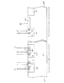
図1は、本発明によるCMOS型固体撮像装置の一実施形態を、画素部と周辺CMOS回路部を含む断面で示した図である。ここで、(A)は画素部、(B)は周辺CMOS回路部で、共通の低濃度p基板100の上に構成されている。110、120はCMOS回路部のp型及びn型ツインウェルである。また、pウェル110は、画素部ではトランジスタ部のpウェルとしても用いられるが、画素部のうち、フォトダイオードの下側のみ形成されない。なお、フォトダイオード用n+層130は、画素のトランジスタ部及び周辺CMOS回路部n型トランジスタのソース/ドレイン用n+層131と、同じであっても、あるいは異なる層とされてもよい。また、画素部は増幅型であっても、非増幅型であってもよい。なお、141は、周辺CMOS回路部p型トランジスタのソース/ドレイン用p+層である。
【0034】
図2は、本発明によるCMOS型固体撮像装置の他の実施形態を、画素部と周辺CMOS回路部を含む断面で示した図である。ここで、(A)は画素部、(B)は周辺CMOS回路部で、図1と同じ構成要素には同じ符号を用いる。図1との相違点は、フォトダイオード部下側にCMOS回路部ツインウェル中のnウェル120を用いていることである。
【0035】
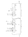
図3は、図1の手法を非増幅型の画素に適用した場合の、画素部平面パターン例及びその断面を示した図である。平面図(a)で、3は画素選択用トランジスタ、5はフォトダイオード、11は画素選択信号線、13は信号線である。CMOS部と同じpウェル110が、トランジスタ3付近には形成されるが、フォトダイオード5の下側には形成されない。pウェル110が形成されない領域は画素毎に分離されている。この分離の様子は、A−A部断面図(b)及びB−B部断面図(c)により、より明確に示される。すなわち、フォトダイオードn+層130の下側のみpウェル110が存在しない。このため、フォトダイオードは直接低濃度p基板100に接する。
【0036】
図4は、図2の手法を非増幅型の画素に適用した場合の、画素部平面パターン例及びその断面を示した図である。図3と同じ構成要素については、同じ符号を用いる。トランジスタ3付近はCMOS部と同じpウェル110が、また、フォトダイオードの下側にはCMOS部と同じnウェル120が、それぞれ形成されている。nウェル120は、pウェル110によって画素毎に分離されている。この分離の様子は、A−A部断面図(b)及びB−B部断面図(c)により、より明確に示される。すなわち、フォトダイオードn+層130の下側に、nウェル120が形成され、このnウェル120は周辺をpウェル110で分離されている。なお、トランジスタ3はpウェル110上に形成される。したがって、nウェル120とpウェル110との境界は、トランジスタ3より少しフォトダイオード側となる。他方、nウェル120は一点鎖線で示す活性領域の外側のフィールド酸化膜側にまで少し伸びた所まで延在させるのが望ましいが、その理由は後述する。
【0037】
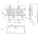
図5は、図1の手法を増幅型の画素に適用した場合の、画素部平面パターン例及びその断面を示した図である。平面図(a)で、1は増幅用トランジスタ、2はリセット用トランジスタ、3は画素選択用トランジスタ、5はフォトダイオード、11は画素選択信号線、12はリセット信号線、13は信号線、14は電源線である。CMOS部と同じpウェル110が、トランジスタ1、2、3の下側には形成されるが、フォトダイオード5の下側には形成されない。pウェル110が形成されない領域は画素毎に分離されている。この分離の様子は、A−A部断面図(b)及びB−B部断面図(c)により、より明確に示される。すなわち、pウェル110はフォトダイオードn+層130の下側のみ存在せず、このため、n+層130は低濃度p基板100に直接接している。
【0038】
図6は、図5(b)に示した断面図をより詳細に示した図である。ここでは、フィールド酸化膜として最も一般的なLOCOSプロセスで形成した場合を考える。また、図6において、一例として、

【0039】
(状態1) dp2=22.5×10⁻⁵cm.
したがって、pウェル上にフォトダイオードを形成した場合(空乏層の厚さ=2.3×10⁻⁵cm)に比べ、空乏層の厚さは10倍となり、少なくとも可視光領域では十分な光電変換効率が確保される。また同時に、空乏層より下側での電荷発生は大変少なくなるから、解像度の劣化やフレア現象は大幅に抑えられる。また、フォトダイオード部の容量は、pウェル内に形成した場合に比べ、(ボトムの容量が支配的として)1/10に低下する。すなわち、電荷電圧変換ゲインは10倍に向上する。
【0040】
なお、図3、図5及び図6の例では、フォトダイオード下側のpウェルの存在しない領域は、一点鎖線で示す活性領域の外側のフィールド酸化膜にまで少し伸びた所まで延在させているが、本発明はこれに限定されることはなく、逆に、活性領域の内側であってもよい(図示せず)。
【0041】
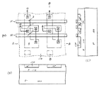
図7は、図2の手法を増幅型の画素に適用した場合の、画素部平面パターン例及びその断面を示した図である。図5と同じ構成要素については、同じ符号を用いる。図5との相違点は、フォトダイオードn+層130の下側にCMOS部と同じnウェル120を形成したことである。nウェル120はpウェル110によって画素毎に分離されている。この分離の様子は、A−A部断面図(b)及びB−B部断面図(c)により、より明確に示される。すなわち、フォトダイオードn+層130の下側に、nウェル120が形成され、このnウェル120は周辺をpウェル110で分離されている。nウェル120とpウェル110との境界は、フォトダイオード5に隣接するトランジスタ2より少しフォトダイオード側となる。他方、nウェル120は一点鎖線で示す活性領域の外側のフィールド酸化膜側にまで少し伸びた所まで延在させるのが望ましいが、その理由を以下で述べる。
【0042】
図8は、図7(b)に示した断面図をより詳細に示した図である。ここでは、フィールド酸化膜として最も一般的なLOCOSプロセスで形成した場合を考える。また、図8において、一例として、
【0043】
【0044】
他方、フォトダイオード周辺のフィールド酸化膜との境界は、結晶欠陥が多いとされているが、従来はここに空乏層が形成されるため、暗電流の発生が避けられなかった。本発明では、図8に示すように、nウェル層のフィールド側への被り量■を、dn1とバーズビーク量(1例として0.5μm)の和より大きく、例えば、1μm程度とすれば、結晶欠陥が多いとされるバーズビーク周辺はn層120の中性領域となるから、暗電流の発生が抑えられる。すなわち、画質劣化の原因となる、暗電流による白点欠陥やザラ状固定パターンノイズが抑圧される。
【0045】
【発明の効果】
以上詳述したように、本発明のCMOS型固体撮像装置によれば、空乏層深さが増すことにより光学的有効深さが拡大し、光電変換の効率を大きく増大できる。また、特に増幅型CMOS固体撮像装置では、フォトダイオード容量の低下により電荷電圧変換効率が増大し、前記光電変換効率の増大と相俟って、感度が大幅に増大する。他方、空乏層深さの拡大は、各画素で発生する電荷を大部分その画素に集めることに寄与し、解像度の向上とフレアの抑圧に効果がある。更に、一般にはフォトダイオード周辺のフィールド酸化膜境界では結晶欠陥が多く、しかもここに空乏層が形成されるため、暗電流が発生しやすい。しかし、本発明により、この境界領域をウェル中性領域で覆うことが可能となり、暗電流の発生は大幅に抑えられる。
【0046】
以上、本発明により、簡単な構成で、極めて高感度、高解像度、低フレアで、更に、低暗電流のCMOS型固体撮像装置を形成することが可能となる。
【0047】
また、本発明では、標準のCMOSプロセスのまま画素形成が可能なため、周辺の駆動回路部や信号処理部等を一体化することが容易で、CMOSイメージセンサの特徴をそのまま残すことが可能となる。
【0048】
以上により、本発明の実用上の効果は絶大である。
【図面の簡単な説明】
【図1】本発明によるCMOS型固体撮像装置の一実施形態を、画素部と周辺CMOS回路部を含む断面で示した図である。
【図2】本発明によるCMOS型固体撮像装置の他の実施形態を、画素部と周辺CMOS回路部を含む断面で示した図である。
【図3】図1の手法を非増幅型の画素に適用した場合の画素部平面パターン例及びその断面を示す図であり、(a)は平面図、(b)は平面図(a)に於けるA−A部断面図、(c)は平面図(a)に於けるB−B部断面図である。
【図4】図2の手法を非増幅型の画素に適用した場合の画素部平面パターン例及びその断面を示す図であり、(a)は平面図、(b)は平面図(a)に於けるA−A部断面図、(c)は平面図(a)に於けるB−B部断面図である。
【図5】図1の手法を増幅型の画素に適用した場合の画素部平面パターン例及びその断面を示す図であり、(a)は平面図、(b)は平面図(a)に於けるA−A部断面図、(c)は平面図(a)に於けるB−B部断面図である。
【図6】図5に示す本発明のCMOS型固体撮像装置の、画素部における空乏層の様子を示す図である。
【図7】図2の手法を増幅型の画素に適用した場合の画素部平面パターン例及びその断面を示す図であり、(a)は平面図、(b)は平面図(a)に於けるA−A部断面図、(c)は平面図(a)に於けるB−B部断面図である。
【図8】図7に示す本発明のCMOS型固体撮像装置の、画素部における空乏層の様子を示す図である。
【図9】本発明が適用される非増幅型CMOS型固体撮像装置の画素部の構成を示す図である。
【図10】従来の非増幅型CMOS型固体撮像装置の画素部平面パターン例及びその断面を示す図であり、(a)は平面図、(b)は平面図(a)に於けるA−A部断面図、(c)は平面図(a)に於けるB−B部断面図である。
【図11】本発明が適用される増幅型CMOS型固体撮像装置の画素部の構成を示す図である。
【図12】従来の増幅型CMOS型固体撮像装置の画素部平面パターン例及びその断面を示す図であり、(a)は平面図、(b)は平面図(a)に於けるA−A部断面図、(c)は平面図(a)に於けるB−B部断面図である。
【図13】従来のCMOS型固体撮像装置のフォトダイオード部に於ける、光電変換の様子を示す図である。
【図14】従来の他の増幅型CMOS型固体撮像装置の画素部構成を示す図である。
【図15】図14に示す従来のCMOS型固体撮像装置に於ける、フォトダイオード部の形成方法を説明する図である。
【符号の説明】
100 p基板
110 pウェル
120 nウェル
130 フォトダイオード用n+層
131 n型トランジスタのソース/ドレイン用n+層
141 p型トランジスタのソース/ドレイン用p+層[0001]
TECHNICAL FIELD OF THE INVENTION
The present invention relates to a CMOS solid-state imaging device having a highly sensitive pixel configuration.
[0002]
[Prior art]
A CMOS image sensor in which an image sensor is formed using a CMOS process has been proposed. This includes a passive PPS (Passive Pixel Sensor) that reads out the signal charge generated in each pixel as it is, and an active APS (Active Pixel Sensor) that amplifies and reads out the signal charge for each pixel. In each case, a photodiode having a pn junction is generally used for the photoelectric conversion unit.
[0003]
In the PPS type, as shown in FIG. 9, a signal charge from a photodiode is switched by one MOS transistor in the same pixel and read out to a signal line as it is. Here, 5 is a photodiode, 3 is a pixel selection MOS transistor, 11 is a pixel selection clock line, and 13 is a signal line.
[0004]
FIG. 10 is a plan view of the example of the plane pattern of FIG. 9, showing a plan view (a) of one pixel, a cross-sectional view (b) of an AA portion thereof, and a cross-sectional view (c) of a BB portion thereof. Each component of the
[0005]
In the APS type, it is necessary to form a photoelectric conversion unit, an amplification unit, a pixel selection unit, and a reset unit in one pixel. Usually, in addition to a photodiode (PD), three to four MOS transistors (T) Is used. FIG. 11 shows a configuration of one pixel in the case of the PD + 3T method (Mabuchi et al., “A 340,000-pixel CMOS image sensor supporting 1 / inch VGA”, Technical Report of the Institute of Image Information and Television Engineers, IPU 97-13, March 1997). Here, 5 is a photodiode, 1 is an amplifying unit, 2 is a reset unit, 3 is a pixel selection unit, 11 is a pixel selection clock line, 12 is a reset clock line, 13 is a signal line, and 14 is a power supply line.
[0006]
FIG. 12 is a plan view of the example of the plane pattern of FIG. 11, showing a plan view (a) of one pixel, a cross-sectional view (b) of an AA portion thereof, and a cross-sectional view (c) of a BB portion thereof. The components of the
[0007]
9 to 12,
[0008]
[Problems to be solved by the invention]
The light incident on the pn junction of the photodiode is photoelectrically converted on average up to the penetration depth Lp to generate an electron / hole pair. Of these, the amount of electrons effectively stored as signal charges in the surface-side n-layer is the sum of the following three components. (1) All electrons generated in the depletion layer formed at the pn junction interface, (2) electrons corresponding to the amount of holes generated in the neutral region of the n-layer reaching the end of the depletion layer at the junction interface, (3) ▼ The amount of electrons generated in the neutral region of the p-layer reached the depletion layer edge at the junction interface. Therefore, in order to increase the sensitivity, it is most efficient to enlarge the depletion layer region (1). The component (2) is preferably such that the diffusion length of holes in the n-layer is larger than the n-layer junction depth Xj. The component (3) is better as the diffusion length of electrons in the p-layer is increased. However, if the diffusion length of electrons in the p-layer is increased, interference between adjacent pixels also increases, causing a reduction in resolution and a flare phenomenon, which is not a preferable method in practice.
[0009]
9 to 12, the
[0010]
A value adopted in a general CMOS process is a p-well concentration: about Np = 1 × 10 17 cm −3 , and when a bias voltage: Vb = 3 V, a thickness of a depletion layer: Xdep = 0.23 μm It becomes. In a recent general CMOS process, the junction depth Xj is as small as about 0.15 μm. Taking the case where the wavelength of visible light, for example, having the highest visibility = 550 nm as the incident light, is an example, the penetration depth Lp is about 1.5 μm. That is, the depletion layer region that is most efficient for photoelectric conversion is only about 15% of the effective photoelectric conversion region, and the surface n + layer region is only about 10%. Most of the depletion layer region is photoelectric conversion in the p well and the p substrate region below it. If the diffusion length of electrons in the p-well is short, the sensitivity is lowered, and if the diffusion length is long, the resolution is reduced and the flare phenomenon is caused.
[0011]
FIG. 14 shows a technique disclosed in Japanese Unexamined Patent Application Publication No. 9-232555 as a countermeasure against the above-mentioned problem of the prior art. The circuit configuration of FIG. 14 is the same as that of FIG. 11, and the same reference numerals are used for the same parts as in FIG. 11 for simplicity. A characteristic of FIG. 14 is the structure of the
[0012]
However, this method has the following problems. First, providing a p-well on an n-substrate and forming an n-type transistor or an np-junction photodiode therein further facilitates the occurrence of an npn vertical bipolar operation. In particular, in the light receiving section, it is difficult to contact the p-well at an intermediate depth with high density from the surface side because it is necessary to secure a photodiode area, so that the p-well potential is likely to be incompletely fixed. This tends to cause an npn bipolar operation, resulting in a malfunction.
[0013]
In order to reduce the junction capacitance of the photodiode, the concentration of the n-
[0014]
When there is no n-layer 220: Cj = 46 nF / cm 2
When N n = 1 × 10 18 cm −3 : Cj = 44 nF / cm 2
When N n = 1 × 10 17 cm −3 : Cj = 33 nF / cm 2
When N n = 1 × 10 16 cm −3 : Cj = 14 nF / cm 2
That is, the effect of junction capacitance reduction appears at the concentration N n is the case sufficiently smaller than the concentration N p.
[0015]
However, the concentration of the n layer 220: an N n, p well concentration: Np be formed below is very difficult. That is, as shown in FIG. 15, when the n-
[0016]
The present invention has been devised in view of the above problems, and does not need to introduce a vertical bipolar structure into the light receiving unit, and does not need to introduce any special ion implantation step into a normal CMOS process, and has high sensitivity. An object of the present invention is to provide an ideal CMOS type solid-state imaging device which can realize a structure of a photodiode section capable of achieving high resolution and low flare with low dark current.
[0017]
[Means for Solving the Problems]
In order to achieve the above object, in a CMOS solid-state imaging device according to the present invention, a plurality of pixels, a first layer of a first conductivity type, and a second layer of a second conductivity type are provided on a surface of a semiconductor substrate of the first conductivity type. 2 layer, furthermore, a twin-well type in which a second conductivity type first MOS transistor formed on the first layer and a first conductivity type second MOS transistor formed on the second layer are formed. The pixel has a CMOS structure, and each of the pixels has a photodiode made of a third layer of a second conductivity type and a third MOS transistor of a second conductivity type. A layer is formed, and the first layer is not formed under the photodiode;
And the first layer of the first conductivity type has a higher concentration than the semiconductor substrate of the first conductivity type;
And the pixel is of an amplification type for amplifying a signal in the pixel, and the plurality of the third MOS transistors are provided for each pixel.
Further, the first layer in the twin-well type CMOS structure is used as a lower first layer of the third MOS transistor;
It is characterized by.
[0018]
Further, the second layer may be formed on the lower side of the photodiode without the first layer.
[0019]
Further, the first layer and the second layer are configured to have a concentration that is at least 10 times higher than the concentration of the semiconductor substrate.
[0020]
Further, it is configured such that a boundary between a second layer formed below the photodiode and a first layer formed below the third MOS transistor is formed outside the photodiode region. Is desirable.
[0021]
Further, it is preferable that the second layer formed below the photodiode is formed so as to be isolated for each pixel.
[0022]
The pixel may be a non-amplification type that does not perform signal amplification in the pixel, and the number of the third MOS transistors may be one or more for each pixel.
[0023]
Alternatively, the pixel may be of an amplification type that amplifies a signal in the pixel, and a plurality of the third MOS transistors may be provided for each pixel.
[0024]
Furthermore, the third layer may be formed of the same layer as the source / drain part of the third MOS transistor.
[0025]
Alternatively, the third layer may be formed of a layer different from the source / drain part of the third MOS transistor.
[0026]
In such a CMOS solid-state imaging device of the present invention, a plurality of pixels and a twin-well CMOS structure are provided on a semiconductor substrate, and the transistor portion of each pixel is the same as the substrate of the CMOS structure twin well. A well of higher conductivity than the substrate is formed of the conductivity type, and the well does not exist below the photodiode portion. For this reason, the pn junction for photoelectric conversion is formed directly on the low-concentration substrate, so that the thickness of the depletion layer on the substrate side is very large.
[0027]
Furthermore, when a well of the conductivity type opposite to the substrate is formed in the twin well of the CMOS structure below the photodiode, the surface side layer of the pn junction for photoelectric conversion is the same as the photodiode layer. , And the well layer thereunder, so that the junction depth is greatly increased. Further, since the junction is formed directly on the low-concentration substrate, the thickness of the depletion layer on the substrate side is very large.
[0028]
In these methods, the optically effective depth becomes very large due to the expansion of the depletion layer, and the efficiency of photoelectric conversion is significantly increased. Further, the junction on the low-concentration substrate causes a large decrease in the junction capacitance and increases the potential change of the photodiode unit per generated charge amount. That is, the charge-voltage conversion gain is increased. This leads to a further improvement in sensitivity especially in the case of an amplification type solid-state imaging device.
[0029]
Furthermore, since the depletion layer is formed deeply into the substrate, most of the charge generated in each pixel region is collected as signal charge, and diffusion to peripheral pixels is reduced, so that resolution is improved and flare is reduced. It is also effective for prevention.
[0030]
Further, the above structure can be formed without any change in the basic CMOS process because the CMOS part well is used for the photodiode part.
[0031]
As described above, according to the present invention, a CMOS type solid-state imaging device having extremely high sensitivity, high resolution, and low flare can be configured with a standard CMOS process.
[0032]
BEST MODE FOR CARRYING OUT THE INVENTION
Hereinafter, embodiments of the present invention will be described in detail with reference to the drawings.
[0033]
FIG. 1 is a diagram showing an embodiment of a CMOS solid-state imaging device according to the present invention in a cross section including a pixel portion and a peripheral CMOS circuit portion. Here, (A) is a pixel portion, and (B) is a peripheral CMOS circuit portion, which is formed on a common low-
[0034]
FIG. 2 is a diagram showing another embodiment of the CMOS solid-state imaging device according to the present invention in a cross section including a pixel portion and a peripheral CMOS circuit portion. Here, (A) is a pixel portion, (B) is a peripheral CMOS circuit portion, and the same components as those in FIG. The difference from FIG. 1 is that an n-well 120 in the CMOS circuit unit twin well is used below the photodiode unit.
[0035]
FIG. 3 is a diagram showing an example of a pixel portion plane pattern and a cross section thereof when the method of FIG. 1 is applied to a non-amplification type pixel. In the plan view (a), 3 is a pixel selection transistor, 5 is a photodiode, 11 is a pixel selection signal line, and 13 is a signal line. The same p-well 110 as the CMOS part is formed near the
[0036]
FIG. 4 is a diagram showing an example of a pixel portion plane pattern and a cross section thereof when the method of FIG. 2 is applied to a non-amplification type pixel. The same reference numerals are used for the same components as those in FIG. A p-
[0037]
FIG. 5 is a diagram showing an example of a pixel portion plane pattern and a cross section thereof when the method of FIG. 1 is applied to an amplification type pixel. In the plan view (a), 1 is an amplification transistor, 2 is a reset transistor, 3 is a pixel selection transistor, 5 is a photodiode, 11 is a pixel selection signal line, 12 is a reset signal line, 13 is a signal line, 14 Is a power supply line. The same p-well 110 as the CMOS part is formed below the
[0038]
FIG. 6 is a diagram showing the cross-sectional view shown in FIG. 5B in more detail. Here, it is assumed that the field oxide film is formed by the most general LOCOS process. In FIG. 6, as an example,
[0039]
(State 1) d p2 = 22.5 × 10 −5 cm.
Therefore, the thickness of the depletion layer is ten times that of the case where the photodiode is formed on the p-well (thickness of the depletion layer = 2.3 × 10 −5 cm), and sufficient photoelectric conversion at least in the visible light region. Efficiency is ensured. At the same time, the generation of electric charges below the depletion layer is very small, so that the deterioration of the resolution and the flare phenomenon can be greatly suppressed. Further, the capacitance of the photodiode portion is reduced to 1/10 (assuming that the bottom capacitance is dominant) as compared with the case where the photodiode portion is formed in the p-well. That is, the charge-voltage conversion gain is improved by a factor of ten.
[0040]
In the examples shown in FIGS. 3, 5 and 6, the region under the photodiode where no p-well exists is extended to a position slightly extending to the field oxide film outside the active region indicated by a dashed line. However, the present invention is not limited to this, and conversely, it may be inside the active region (not shown).
[0041]
FIG. 7 is a diagram showing an example of a pixel portion plane pattern and its cross section when the method of FIG. 2 is applied to an amplification type pixel. The same reference numerals are used for the same components as those in FIG. The difference from FIG. 5 is that the same n-well 120 as the CMOS part is formed below the photodiode n +
[0042]
FIG. 8 is a diagram showing the cross-sectional view shown in FIG. 7B in more detail. Here, it is assumed that the field oxide film is formed by the most general LOCOS process. In FIG. 8, as an example,
[0043]
[0044]
On the other hand, the boundary between the photodiode and the field oxide film around the photodiode is said to have many crystal defects. However, conventionally, a depletion layer is formed here, so that generation of dark current is unavoidable. In the present invention, as shown in FIG. 8, fog amount to n-well layer field side of the ■, d n1 and bird's beak amount greater than the sum of (0.5 [mu] m as an example), for example, it is about 1 [mu] m, The periphery of the bird's beak, which is considered to have many crystal defects, becomes a neutral region of the n-
[0045]
【The invention's effect】
As described in detail above, according to the CMOS solid-state imaging device of the present invention, the optically effective depth is increased by increasing the depletion layer depth, and the photoelectric conversion efficiency can be greatly increased. In particular, in an amplification type CMOS solid-state imaging device, the charge-voltage conversion efficiency increases due to a decrease in the photodiode capacitance, and the sensitivity greatly increases in conjunction with the increase in the photoelectric conversion efficiency. On the other hand, the increase in the depth of the depletion layer contributes to collecting most of the charge generated in each pixel in the pixel, and is effective in improving the resolution and suppressing flare. Furthermore, in general, there are many crystal defects at the boundary of the field oxide film around the photodiode, and a depletion layer is formed here, so that a dark current is easily generated. However, according to the present invention, the boundary region can be covered with the well neutral region, and the generation of dark current can be greatly suppressed.
[0046]
As described above, according to the present invention, it is possible to form a CMOS solid-state imaging device with a very simple configuration, extremely high sensitivity, high resolution, low flare, and low dark current.
[0047]
Further, according to the present invention, since pixels can be formed in a standard CMOS process, it is easy to integrate peripheral drive circuit units, signal processing units, and the like, and the features of a CMOS image sensor can be left as they are. Become.
[0048]
As described above, the practical effect of the present invention is enormous.
[Brief description of the drawings]
FIG. 1 is a diagram showing an embodiment of a CMOS solid-state imaging device according to the present invention in a cross section including a pixel portion and a peripheral CMOS circuit portion.
FIG. 2 is a diagram showing another embodiment of a CMOS solid-state imaging device according to the present invention in a cross section including a pixel portion and a peripheral CMOS circuit portion.
FIGS. 3A and 3B are diagrams showing an example of a pixel unit plane pattern and a cross section thereof when the method of FIG. 1 is applied to a non-amplification type pixel, where FIG. 3A is a plan view and FIG. FIG. 2C is a cross-sectional view taken along the line AA in FIG. 2, and FIG.
4A and 4B are diagrams showing an example of a pixel unit plane pattern and a cross section thereof when the method of FIG. 2 is applied to a non-amplification type pixel, wherein FIG. 4A is a plan view and FIG. FIG. 2C is a cross-sectional view taken along the line AA in FIG. 2, and FIG.
5A and 5B are diagrams showing an example of a pixel portion plane pattern and a cross section when the method of FIG. 1 is applied to an amplification type pixel, wherein FIG. 5A is a plan view, and FIG. FIG. 3C is a cross-sectional view taken along the line AA in FIG.
FIG. 6 is a diagram showing a state of a depletion layer in a pixel portion of the CMOS solid-state imaging device of the present invention shown in FIG.
7A and 7B are diagrams showing an example of a pixel unit plane pattern and a cross section when the method of FIG. 2 is applied to an amplification type pixel, wherein FIG. 7A is a plan view and FIG. FIG. 3C is a cross-sectional view taken along the line AA in FIG.
8 is a diagram showing a state of a depletion layer in a pixel portion of the CMOS solid-state imaging device of the present invention shown in FIG.
FIG. 9 is a diagram illustrating a configuration of a pixel portion of a non-amplification type CMOS solid-state imaging device to which the present invention is applied;
10A and 10B are diagrams illustrating an example of a pixel unit planar pattern and a cross section of a conventional non-amplification type CMOS solid-state imaging device, wherein FIG. 10A is a plan view, and FIG. FIG. 2C is a cross-sectional view of the portion A, and FIG.
FIG. 11 is a diagram showing a configuration of a pixel portion of an amplification type CMOS solid-state imaging device to which the present invention is applied.
12A and 12B are diagrams showing an example of a pixel unit plane pattern and a cross section of a conventional amplification type CMOS solid-state imaging device, wherein FIG. 12A is a plan view, and FIG. 12B is a plan view AA in FIG. FIG. 3C is a cross-sectional view of a part BB in the plan view of FIG.
FIG. 13 is a diagram illustrating a state of photoelectric conversion in a photodiode section of a conventional CMOS solid-state imaging device.
FIG. 14 is a diagram illustrating a configuration of a pixel portion of another conventional amplification type CMOS solid-state imaging device.
FIG. 15 is a diagram for explaining a method of forming a photodiode section in the conventional CMOS solid-state imaging device shown in FIG.
[Explanation of symbols]
Reference Signs List 100 p substrate 110 p well 120 n well 130 n + layer for photodiode 131 n + layer for source / drain of n-type transistor 141 p + layer for source / drain of p-type transistor
Claims (4)
および、前記第1導電型の第1の層は、前記第1導電型の半導体基板よりも高濃度であること、
および、前記画素は画素内で信号増幅を行う増幅型であり、前記第3MOSトランジスタは各画素当たり複数個であること、
さらに、前記ツインウェル型CMOS構造における第1の層は前記第3MOSトランジスタの下側の第1の層として用いていること、
を特徴とするCMOS型固体撮像装置。A plurality of pixels, a first layer of the first conductivity type, a second layer of the second conductivity type, and a second conductive layer formed on the first layer are formed on the surface of the semiconductor substrate of the first conductivity type. A first conductivity type MOS transistor and a first conductivity type second MOS transistor formed on the second layer, having a twin-well type CMOS structure, wherein each pixel has a second conductivity type third layer. And a third MOS transistor of a second conductivity type. The first layer is formed below the third MOS transistor, and the first layer is formed below the photodiode. Layer is not formed,
And the first layer of the first conductivity type has a higher concentration than the semiconductor substrate of the first conductivity type;
And the pixel is of an amplification type for amplifying a signal in the pixel, and the plurality of the third MOS transistors are provided for each pixel.
Further, a first layer in the twin-well type CMOS structure is used as a first layer below the third MOS transistor;
A CMOS type solid-state imaging device characterized by the above-mentioned.
および、前記ツインウェル型CMOS構造における第2の層は前記フォトダイオードの下側の第2の層として用いていること、
を特徴とするCMOS型固体撮像装置。2. The CMOS solid-state imaging device according to claim 1, wherein the second layer is formed below the photodiode.
A second layer in the twin-well CMOS structure is used as a second layer below the photodiode;
A CMOS solid-state imaging device characterized by the above-mentioned.
Priority Applications (4)
| Application Number | Priority Date | Filing Date | Title |
|---|---|---|---|
| JP11122298A JP3554483B2 (en) | 1998-04-22 | 1998-04-22 | CMOS solid-state imaging device |
| KR1019990014359A KR100291285B1 (en) | 1998-04-22 | 1999-04-22 | Cmos type solid imaging device |
| US09/296,344 US6448104B1 (en) | 1998-04-22 | 1999-04-22 | CMOS type solid imaging device |
| US10/198,210 US6642562B2 (en) | 1998-04-22 | 2002-07-17 | CMOS type solid imaging device |
Applications Claiming Priority (1)
| Application Number | Priority Date | Filing Date | Title |
|---|---|---|---|
| JP11122298A JP3554483B2 (en) | 1998-04-22 | 1998-04-22 | CMOS solid-state imaging device |
Publications (2)
| Publication Number | Publication Date |
|---|---|
| JPH11307753A JPH11307753A (en) | 1999-11-05 |
| JP3554483B2 true JP3554483B2 (en) | 2004-08-18 |
Family
ID=14555642
Family Applications (1)
| Application Number | Title | Priority Date | Filing Date |
|---|---|---|---|
| JP11122298A Expired - Fee Related JP3554483B2 (en) | 1998-04-22 | 1998-04-22 | CMOS solid-state imaging device |
Country Status (3)
| Country | Link |
|---|---|
| US (2) | US6448104B1 (en) |
| JP (1) | JP3554483B2 (en) |
| KR (1) | KR100291285B1 (en) |
Families Citing this family (34)
| Publication number | Priority date | Publication date | Assignee | Title |
|---|---|---|---|---|
| JP3554483B2 (en) * | 1998-04-22 | 2004-08-18 | シャープ株式会社 | CMOS solid-state imaging device |
| US6727521B2 (en) * | 2000-09-25 | 2004-04-27 | Foveon, Inc. | Vertical color filter detector group and array |
| US6534335B1 (en) * | 1999-07-22 | 2003-03-18 | Micron Technology, Inc. | Optimized low leakage diodes, including photodiodes |
| JP3624140B2 (en) * | 1999-08-05 | 2005-03-02 | キヤノン株式会社 | Photoelectric conversion device and method for manufacturing the same, digital still camera or digital video camera |
| KR100390822B1 (en) * | 1999-12-28 | 2003-07-10 | 주식회사 하이닉스반도체 | Method for reducing dark current in image sensor |
| JP4945861B2 (en) * | 2000-09-05 | 2012-06-06 | 株式会社ニコン | Thermal displacement element and radiation detector using the same |
| US6713796B1 (en) * | 2001-01-19 | 2004-03-30 | Dalsa, Inc. | Isolated photodiode |
| JP4779218B2 (en) * | 2001-03-08 | 2011-09-28 | 日本ビクター株式会社 | CMOS image sensor |
| JP3759435B2 (en) * | 2001-07-11 | 2006-03-22 | ソニー株式会社 | XY address type solid-state imaging device |
| JP2003092424A (en) * | 2001-07-12 | 2003-03-28 | Sharp Corp | Separable photo detector, circuit-containing photo detector and optical disc device |
| JP2003298038A (en) * | 2002-04-05 | 2003-10-17 | Canon Inc | Photoelectric conversion element and solid-state imaging device using the same |
| JP4313990B2 (en) | 2002-07-02 | 2009-08-12 | シャープ株式会社 | Solid-state imaging device |
| EP1391932A1 (en) * | 2002-08-22 | 2004-02-25 | STMicroelectronics Limited | Solid state image sensor |
| US7205593B2 (en) * | 2002-09-13 | 2007-04-17 | Matsushita Electric Industrial Co., Ltd. | MOS image pick-up device and camera incorporating the same |
| EP1465258A1 (en) * | 2003-02-21 | 2004-10-06 | STMicroelectronics Limited | CMOS image sensors |
| WO2004099740A2 (en) * | 2003-05-08 | 2004-11-18 | Council For The Central Laboratory Of The Research Councils | Accelerated particle and high energy radiation sensor |
| JP2005005573A (en) * | 2003-06-13 | 2005-01-06 | Fujitsu Ltd | Image pickup device |
| US7009227B2 (en) * | 2003-06-16 | 2006-03-07 | Micron Technology, Inc. | Photodiode structure and image pixel structure |
| JP2005244096A (en) * | 2004-02-27 | 2005-09-08 | Asahi Kasei Microsystems Kk | Solid-state image sensing element and its manufacturing method |
| EP1865555A4 (en) | 2005-03-28 | 2010-10-20 | Fujitsu Semiconductor Ltd | Image pickup device |
| CN100565892C (en) * | 2005-04-29 | 2009-12-02 | 皇家飞利浦电子股份有限公司 | Manufacture method with semiconductor device and this device of imageing sensor |
| KR20070033718A (en) * | 2005-09-22 | 2007-03-27 | 동부일렉트로닉스 주식회사 | CMOS image sensor and its manufacturing method |
| JP4679340B2 (en) * | 2005-11-11 | 2011-04-27 | 株式会社東芝 | Solid-state imaging device |
| US7728277B2 (en) * | 2005-11-16 | 2010-06-01 | Eastman Kodak Company | PMOS pixel structure with low cross talk for active pixel image sensors |
| KR100660333B1 (en) * | 2005-12-28 | 2006-12-22 | 동부일렉트로닉스 주식회사 | Method for fabricating cmos image sensor |
| EP1857634B8 (en) * | 2006-05-17 | 2013-11-13 | STMicroelectronics (Research & Development) Limited | A variably responsive photosensor |
| JP5109686B2 (en) * | 2007-06-22 | 2012-12-26 | セイコーエプソン株式会社 | Detection device and electronic device |
| JP5109684B2 (en) * | 2007-06-22 | 2012-12-26 | セイコーエプソン株式会社 | Detection device and electronic device |
| JP5109687B2 (en) * | 2007-06-22 | 2012-12-26 | セイコーエプソン株式会社 | Detection device and electronic device |
| JP5109685B2 (en) * | 2007-06-22 | 2012-12-26 | セイコーエプソン株式会社 | Detection device and electronic device |
| KR101621241B1 (en) * | 2009-10-07 | 2016-05-16 | 삼성전자 주식회사 | Image sensor and fabricating method thereof |
| CN102110694B (en) * | 2009-12-29 | 2013-03-27 | 中芯国际集成电路制造(上海)有限公司 | Manufacturing method and structure of CMOS (complementary metal-oxide-semiconductor transistor) image sensor |
| EP2461347A1 (en) | 2010-12-06 | 2012-06-06 | Fei Company | Detector system for transmission electron microscope |
| US10811534B2 (en) * | 2017-12-28 | 2020-10-20 | Texas Instruments Incorporated | Transistors with dual wells |
Family Cites Families (23)
| Publication number | Priority date | Publication date | Assignee | Title |
|---|---|---|---|---|
| DE2945854A1 (en) * | 1979-11-13 | 1981-05-21 | Deutsche Itt Industries Gmbh, 7800 Freiburg | ION IMPLANTATION PROCEDURE |
| US4603471A (en) * | 1984-09-06 | 1986-08-05 | Fairchild Semiconductor Corporation | Method for making a CMOS circuit having a reduced tendency to latch by controlling the band-gap of source and drain regions |
| KR940001429B1 (en) * | 1990-12-11 | 1994-02-23 | 삼성전자 주식회사 | Output device of solid state imager |
| US5384477A (en) * | 1993-03-09 | 1995-01-24 | National Semiconductor Corporation | CMOS latchup suppression by localized minority carrier lifetime reduction |
| JPH07161958A (en) * | 1993-12-09 | 1995-06-23 | Nec Corp | Solid-state image pick up device |
| KR0138352B1 (en) * | 1993-12-17 | 1998-04-28 | 김광호 | A semiconductor device & method for fabricating the same |
| US5376568A (en) * | 1994-01-25 | 1994-12-27 | United Microelectronics Corp. | Method of fabricating high voltage complementary metal oxide semiconductor transistors |
| DE19519743A1 (en) * | 1994-05-31 | 1995-12-07 | Dalsa Inc | Photodetector with circuit controlling CCD electrodes |
| US5547895A (en) * | 1994-08-31 | 1996-08-20 | United Microelectronics Corp. | Method of fabricating a metal gate MOS transistor with self-aligned first conductivity type source and drain regions and second conductivity type contact regions |
| US5637900A (en) * | 1995-04-06 | 1997-06-10 | Industrial Technology Research Institute | Latchup-free fully-protected CMOS on-chip ESD protection circuit |
| US5518938A (en) * | 1995-05-08 | 1996-05-21 | United Microelectronics Corporation | Process for fabricating a CMOS transistor having high-voltage metal-gate |
| US5486482A (en) * | 1995-05-09 | 1996-01-23 | United Microelectronics Corporation | Process for fabricating metal-gate CMOS transistor |
| JP2751895B2 (en) * | 1995-10-31 | 1998-05-18 | 日本電気株式会社 | Method for manufacturing semiconductor device |
| US5783470A (en) * | 1995-12-14 | 1998-07-21 | Lsi Logic Corporation | Method of making CMOS dynamic random-access memory structures and the like |
| JPH09232555A (en) | 1996-02-21 | 1997-09-05 | Sony Corp | Image sensor |
| US5702988A (en) * | 1996-05-02 | 1997-12-30 | Taiwan Semiconductor Manufacturing Company, Ltd. | Blending integrated circuit technology |
| US6218895B1 (en) * | 1997-06-20 | 2001-04-17 | Intel Corporation | Multiple well transistor circuits having forward body bias |
| US5898196A (en) * | 1997-10-10 | 1999-04-27 | International Business Machines Corporation | Dual EPI active pixel cell design and method of making the same |
| US6169318B1 (en) * | 1998-02-23 | 2001-01-02 | Polaroid Corporation | CMOS imager with improved sensitivity |
| US6218708B1 (en) * | 1998-02-25 | 2001-04-17 | Sun Microsystems, Inc. | Back-biased MOS device and method |
| JP3554483B2 (en) * | 1998-04-22 | 2004-08-18 | シャープ株式会社 | CMOS solid-state imaging device |
| US6172899B1 (en) * | 1998-05-08 | 2001-01-09 | Micron Technology. Inc. | Static-random-access-memory cell |
| US6184557B1 (en) * | 1999-01-28 | 2001-02-06 | National Semiconductor Corporation | I/O circuit that utilizes a pair of well structures as resistors to delay an ESD event and as diodes for ESD protection |
-
1998
- 1998-04-22 JP JP11122298A patent/JP3554483B2/en not_active Expired - Fee Related
-
1999
- 1999-04-22 US US09/296,344 patent/US6448104B1/en not_active Expired - Lifetime
- 1999-04-22 KR KR1019990014359A patent/KR100291285B1/en not_active IP Right Cessation
-
2002
- 2002-07-17 US US10/198,210 patent/US6642562B2/en not_active Expired - Lifetime
Also Published As
| Publication number | Publication date |
|---|---|
| KR19990083392A (en) | 1999-11-25 |
| KR100291285B1 (en) | 2001-05-15 |
| US20020045306A1 (en) | 2002-04-18 |
| US6642562B2 (en) | 2003-11-04 |
| US20020179907A1 (en) | 2002-12-05 |
| JPH11307753A (en) | 1999-11-05 |
| US6448104B1 (en) | 2002-09-10 |
Similar Documents
| Publication | Publication Date | Title |
|---|---|---|
| JP3554483B2 (en) | CMOS solid-state imaging device | |
| US10224362B2 (en) | Solid-state image pickup element and image pickup apparatus | |
| US6649948B2 (en) | Solid-state image sensor of a MOS structure | |
| US9620545B2 (en) | Solid-state image pickup device and method for producing the same | |
| US7329557B2 (en) | Method of manufacturing solid-state imaging device with P-type diffusion layers | |
| US7151287B1 (en) | Minimizing the effect of directly converted x-rays in x-ray imagers | |
| JP4239980B2 (en) | Infrared solid-state imaging device and manufacturing method thereof | |
| JP2006237622A (en) | Improvement of quantum efficiency in active pixel sensor | |
| KR100237133B1 (en) | Photoelectric conversion apparatus and image reading apparatus | |
| JP2004259733A (en) | Solid-state image pickup device | |
| US20240121530A1 (en) | Light detector | |
| US7312484B1 (en) | Pixel having an oxide layer with step region | |
| KR100583935B1 (en) | Solid-state imaging device | |
| US20070102780A1 (en) | Low dark current cmos image sensor pixel having a photodiode isolated from field oxide | |
| JP5581698B2 (en) | Solid-state image sensor | |
| US7348651B2 (en) | Pinned photodiode fabricated with shallow trench isolation | |
| US6881992B2 (en) | CMOS pixel design for minimization of defect-induced leakage current | |
| JP2007518283A (en) | Pixel structure of high sensitivity CMOS image sensor | |
| US7173299B1 (en) | Photodiode having extended well region | |
| US6372607B1 (en) | Photodiode structure | |
| JPH11251567A (en) | Photoelectric converter |
Legal Events
| Date | Code | Title | Description |
|---|---|---|---|
| TRDD | Decision of grant or rejection written | ||
| A01 | Written decision to grant a patent or to grant a registration (utility model) |
Free format text: JAPANESE INTERMEDIATE CODE: A01 Effective date: 20040427 |
|
| A61 | First payment of annual fees (during grant procedure) |
Free format text: JAPANESE INTERMEDIATE CODE: A61 Effective date: 20040507 |
|
| R150 | Certificate of patent or registration of utility model |
Free format text: JAPANESE INTERMEDIATE CODE: R150 |
|
| FPAY | Renewal fee payment (event date is renewal date of database) |
Free format text: PAYMENT UNTIL: 20080514 Year of fee payment: 4 |
|
| FPAY | Renewal fee payment (event date is renewal date of database) |
Free format text: PAYMENT UNTIL: 20090514 Year of fee payment: 5 |
|
| FPAY | Renewal fee payment (event date is renewal date of database) |
Free format text: PAYMENT UNTIL: 20100514 Year of fee payment: 6 |
|
| FPAY | Renewal fee payment (event date is renewal date of database) |
Free format text: PAYMENT UNTIL: 20110514 Year of fee payment: 7 |
|
| FPAY | Renewal fee payment (event date is renewal date of database) |
Free format text: PAYMENT UNTIL: 20110514 Year of fee payment: 7 |
|
| FPAY | Renewal fee payment (event date is renewal date of database) |
Free format text: PAYMENT UNTIL: 20120514 Year of fee payment: 8 |
|
| FPAY | Renewal fee payment (event date is renewal date of database) |
Free format text: PAYMENT UNTIL: 20120514 Year of fee payment: 8 |
|
| FPAY | Renewal fee payment (event date is renewal date of database) |
Free format text: PAYMENT UNTIL: 20130514 Year of fee payment: 9 |
|
| FPAY | Renewal fee payment (event date is renewal date of database) |
Free format text: PAYMENT UNTIL: 20140514 Year of fee payment: 10 |
|
| LAPS | Cancellation because of no payment of annual fees |