JP3552845B2 - Method for manufacturing semiconductor device - Google Patents
Method for manufacturing semiconductor device Download PDFInfo
- Publication number
- JP3552845B2 JP3552845B2 JP12913596A JP12913596A JP3552845B2 JP 3552845 B2 JP3552845 B2 JP 3552845B2 JP 12913596 A JP12913596 A JP 12913596A JP 12913596 A JP12913596 A JP 12913596A JP 3552845 B2 JP3552845 B2 JP 3552845B2
- Authority
- JP
- Japan
- Prior art keywords
- main surface
- insulating film
- polishing
- wafer
- pressure plate
- Prior art date
- Legal status (The legal status is an assumption and is not a legal conclusion. Google has not performed a legal analysis and makes no representation as to the accuracy of the status listed.)
- Expired - Fee Related
Links
Images


Classifications
-
- H—ELECTRICITY
- H01—ELECTRIC ELEMENTS
- H01L—SEMICONDUCTOR DEVICES NOT COVERED BY CLASS H10
- H01L21/00—Processes or apparatus adapted for the manufacture or treatment of semiconductor or solid state devices or of parts thereof
- H01L21/02—Manufacture or treatment of semiconductor devices or of parts thereof
- H01L21/04—Manufacture or treatment of semiconductor devices or of parts thereof the devices having at least one potential-jump barrier or surface barrier, e.g. PN junction, depletion layer or carrier concentration layer
- H01L21/18—Manufacture or treatment of semiconductor devices or of parts thereof the devices having at least one potential-jump barrier or surface barrier, e.g. PN junction, depletion layer or carrier concentration layer the devices having semiconductor bodies comprising elements of Group IV of the Periodic System or AIIIBV compounds with or without impurities, e.g. doping materials
- H01L21/30—Treatment of semiconductor bodies using processes or apparatus not provided for in groups H01L21/20 - H01L21/26
- H01L21/302—Treatment of semiconductor bodies using processes or apparatus not provided for in groups H01L21/20 - H01L21/26 to change their surface-physical characteristics or shape, e.g. etching, polishing, cutting
- H01L21/304—Mechanical treatment, e.g. grinding, polishing, cutting
-
- B—PERFORMING OPERATIONS; TRANSPORTING
- B24—GRINDING; POLISHING
- B24B—MACHINES, DEVICES, OR PROCESSES FOR GRINDING OR POLISHING; DRESSING OR CONDITIONING OF ABRADING SURFACES; FEEDING OF GRINDING, POLISHING, OR LAPPING AGENTS
- B24B37/00—Lapping machines or devices; Accessories
- B24B37/27—Work carriers
- B24B37/30—Work carriers for single side lapping of plane surfaces
-
- H—ELECTRICITY
- H01—ELECTRIC ELEMENTS
- H01L—SEMICONDUCTOR DEVICES NOT COVERED BY CLASS H10
- H01L21/00—Processes or apparatus adapted for the manufacture or treatment of semiconductor or solid state devices or of parts thereof
- H01L21/02—Manufacture or treatment of semiconductor devices or of parts thereof
- H01L21/04—Manufacture or treatment of semiconductor devices or of parts thereof the devices having at least one potential-jump barrier or surface barrier, e.g. PN junction, depletion layer or carrier concentration layer
- H01L21/18—Manufacture or treatment of semiconductor devices or of parts thereof the devices having at least one potential-jump barrier or surface barrier, e.g. PN junction, depletion layer or carrier concentration layer the devices having semiconductor bodies comprising elements of Group IV of the Periodic System or AIIIBV compounds with or without impurities, e.g. doping materials
- H01L21/30—Treatment of semiconductor bodies using processes or apparatus not provided for in groups H01L21/20 - H01L21/26
- H01L21/31—Treatment of semiconductor bodies using processes or apparatus not provided for in groups H01L21/20 - H01L21/26 to form insulating layers thereon, e.g. for masking or by using photolithographic techniques; After treatment of these layers; Selection of materials for these layers
- H01L21/3105—After-treatment
- H01L21/31051—Planarisation of the insulating layers
- H01L21/31053—Planarisation of the insulating layers involving a dielectric removal step
-
- H—ELECTRICITY
- H01—ELECTRIC ELEMENTS
- H01L—SEMICONDUCTOR DEVICES NOT COVERED BY CLASS H10
- H01L21/00—Processes or apparatus adapted for the manufacture or treatment of semiconductor or solid state devices or of parts thereof
- H01L21/02—Manufacture or treatment of semiconductor devices or of parts thereof
- H01L21/04—Manufacture or treatment of semiconductor devices or of parts thereof the devices having at least one potential-jump barrier or surface barrier, e.g. PN junction, depletion layer or carrier concentration layer
- H01L21/18—Manufacture or treatment of semiconductor devices or of parts thereof the devices having at least one potential-jump barrier or surface barrier, e.g. PN junction, depletion layer or carrier concentration layer the devices having semiconductor bodies comprising elements of Group IV of the Periodic System or AIIIBV compounds with or without impurities, e.g. doping materials
- H01L21/30—Treatment of semiconductor bodies using processes or apparatus not provided for in groups H01L21/20 - H01L21/26
- H01L21/31—Treatment of semiconductor bodies using processes or apparatus not provided for in groups H01L21/20 - H01L21/26 to form insulating layers thereon, e.g. for masking or by using photolithographic techniques; After treatment of these layers; Selection of materials for these layers
- H01L21/3205—Deposition of non-insulating-, e.g. conductive- or resistive-, layers on insulating layers; After-treatment of these layers
- H01L21/321—After treatment
- H01L21/32115—Planarisation
- H01L21/3212—Planarisation by chemical mechanical polishing [CMP]
Description
【0001】
【発明の属する技術分野】
本発明は、半導体装置の製造技術、特に、パターニングされた半導体ウエハ(以下、ウエハという。)のパターニング側主面を化学的機械研磨(Chmical Mechical Polishing)する技術に関する。
【0002】
【従来の技術】
最近、パターニングされたウエハ(以下、パターン付きウエハという。)のパターニング側主面の凹凸を化学的機械研磨によって平坦化する半導体装置の製造方法が提案されている。パターン付きウエハのパターニング側主面の凹凸を化学的機械研磨によって平坦化する技術は、パターニング前のウエハの主面の凹凸を化学的機械研磨によって平坦化する技術と比較して次のような問題点がある。第1の問題点は、研磨量(加工によって除去される量に相当する。)が極端に少ない点である。例えば、パターニング前のウエハにおける研磨量が数十μmであるのに対して、パターン付きウエハにおける研磨量は0.5μm程度である。第2の問題点は、パターン付きウエハの被研磨面であるパターニング側主面の平面度がパターニング前のウエハの被研磨面のそれに比べて遙かに曖昧である点である。これらの問題点を考慮すると、パターン付きウエハのパターニング側主面の凹凸を全面にわたって均一に化学的機械研磨することは困難である。
【0003】
この困難さを克服するパターン付きウエハの化学的機械研磨技術を述べてある例として、日本国特許庁公開特許公報特開平5−74749号公報、特開平6−15563号公報、特開平5−69310号公報、がある。これらの例によって開示された技術はいずれも、圧力流体が密封された弾性体によってパターン付きウエハを押すことにより、パターニング側主面の被研磨面を研磨材面に全体にわたって均一に擦り付けることを原理としている。
【0004】
【発明が解決しようとする課題】
しかしながら、前記原理を利用した従来のパターン付きウエハの化学的機械研磨技術においては、研磨量均一性(後述する。)について0.1μm以下の精度を確保することができないという問題点があることが、本発明者によって明らかにされた。
【0005】
本発明の目的は、パターン付きウエハの被研磨面を高い精度をもって均一に研磨することができる半導体装置の製造技術を提供することにある。
【0006】
本発明の前記ならびにその他の目的と新規な特徴は、本明細書の記述および添付図面から明らかになるであろう。
【0007】
【課題を解決するための手段】
本願において開示される発明のうち代表的なものの概要を説明すれば、次の通りである。
【0008】
すなわち、半導体ウエハのパターニング側主面の表面を化学的機械研磨するに当り、通気路を有する加圧板が通気口を有するウエハ保持ヘッド本体に保持され、かつ、前記加圧板の前記通気口側と反対側の主面に弾性膜が当てがわれているウエハ保持ヘッドが予め用意される。化学的機械研磨する前記半導体ウエハは前記ウエハ保持ヘッドにより前記パターニング側主面と反対側の主面を前記弾性膜に当てがわれた状態で保持される。保持された前記半導体ウエハは前記加圧板によって機械的に押されながら前記通気口に供給された気体の圧力による作用力によって押された状態で、前記パターニング側主面の表面を研磨クロスに擦り付けられて化学的機械研磨される。
【0009】
前記した手段によれば、被研磨面は加圧板の押し力によって研磨クロスに押し付けられて化学的機械研磨されるが、この際、被研磨面に作用する不規則で複雑な歪力は気体の圧力による作用力によって自己整合的に補正されるため、被研磨面の研磨量は全面にわたって均一になる。
【0010】
【発明の実施の形態】
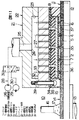
図1は本発明の一実施形態である半導体装置の製造方法に使用されるパターン付きウエハ研磨装置を示す一部省略一部切断正面図である。図2はそのヘッドを示す一部省略分解斜視図である。図3以降は本発明の一実施形態である半導体装置の製造方法を説明する各説明図である。
【0011】
本実施形態において、本発明に係る半導体装置の製造方法には図1に示されているパターン付きウエハ研磨装置が使用される。図1に示されているパターン付きウエハ研磨装置10は、ワークをヘッドによって保持してワークの被研磨面を研磨クロスに研磨材を供給しながら擦り付けて化学的機械研磨する化学的機械研磨装置を使用して構成されている。
【0012】
ここで、本発明に係る半導体装置の製造方法の対象であり、パターン付きウエハ研磨装置10のワークである図3に示されているパターン付きウエハ(以下、ワークという。)1について簡単に説明する。図3に示されているワーク1は外周の一部にオリエンテーションフラット(以下、オリフラという。)3が直線形状に切設されたウエハ(以下、サブストレートという。)2を備えている。サブストレート2のパターニング側主面(以下、表側面という。)における表層領域には半導体素子の一例であるメモリーMが作り込まれているとともに、表面上には金属膜の一例である配線層膜から形成された配線4および絶縁膜の一例である層間絶縁膜5がそれぞれ被着されている。そして、配線4は厚さを有する線分によって形成されているため、その上に被着された層間絶縁膜5の表側面には凹凸部6が下層の配線4の凹凸に倣って形成されている。そこで、本実施形態においては、この層間絶縁膜5の表側面部の一部をパターン付きウエハ研磨装置10によって化学的機械研磨して除去することにより、層間絶縁膜5が平坦化される。したがって、層間絶縁膜5の表側面はパターン付きウエハ研磨装置10によって研磨される被研磨面7を形成する。
【0013】
パターン付きウエハ研磨装置10は研磨工具とヘッドとを備えている。研磨工具11はワーク1の直径よりも充分に大きい半径を有する円盤形状に形成されたベースプレート12を備えており、ベースプレート12は水平面内において回転自在に支持されている。ベースプレート12の下面の中心には垂直方向に配された回転軸13が固定されており、ベースプレート12は回転軸13によって回転駆動されるように構成されている。ベースプレート12の上面には研磨クロス(布)14が全体にわたって均一に貼着されている。研磨クロス14は表面上にポア構造を有する合成樹脂のクロス(布)にコロイダルシリカ等の微細な砥粒が抱え込まれた研磨材であり、表側面によって研磨材面15が形成されている。研磨クロス14による研磨作業に際しては、エッチング液(スラリと称される研磨溶液。以下、スラリという。)が用いられることにより、機械的な研磨(ポリシング)に加えてそのポリシング効果を高めるメカノケミカルポリシング(mechanochemical polishing)が実施される。したがって、研磨工具11の中心線の略真上にはスラリ17を供給するためのスラリ供給ノズル16が配管されている。
【0014】
ヘッド21はワーク1の直径よりも若干大きい直径を有する円盤形状に形成された本体22を備えており、本体22の下面には円形で一定深さの保持穴23が同心円に配されて没設されている。保持穴23の大きさはワーク1の大きさよりも若干大きめに形成されている。保持穴23の中心には通気口24が開設されており、通気口24には通気路25が接続されている。通気路25の他端がエアポンプ26に接続されることにより、通気路25は通気口24に正圧気体としてのエア27を供給する正圧供給路28を構成している。また、通気路25の他端が真空ポンプ29に接続されることにより、通気路25は通気口24に負圧を供給する負圧供給路30を構成している。したがって、通気路25は正圧供給路28と負圧供給路30を兼ねている。正圧供給路28と負圧供給路30との途中には切換弁31が介設されており、正圧供給路28と負圧供給路30とは切換弁31によって切り換えられる。
【0015】
ヘッド本体22の下端面には厚さ方向に貫通した通気孔33を複数本開設された加圧板32が当接されており、加圧板32は保持穴23の開口を閉塞している。加圧板32の外周辺部はヘッド本体22に後記するボルトによって締結されている。加圧板32は剛性を有する材料が使用されて、保持穴23の内径よりも大きくヘッド本体22の外径よりも小さい外径の円盤形状に形成されている。剛性の高い加圧板32はヘッド本体22の下端面に当接されているため、その下面はヘッド21の下降によってワーク1を機械的に押す。複数本の通気孔33は加圧板32の中央部において均等に分布するように配置されている。通気孔33は加圧板32によって仕切りられた保持穴23の上下空間を連通させる通気路を構成している。したがって、通気孔33群は保持穴23の内部において通気口24側と反対側との間で正圧および負圧を流通させる。
【0016】
加圧板32の下端面には弾性膜34が当接されており、弾性膜34は全ての通気孔33の下端開口を閉塞している。弾性膜34の外周辺部はヘッド本体22に後記するボルトによって締結されている。弾性膜34は厚さが約250μmのポリ・エチレン・テレフタレートのフィルムによって形成されている。弾性膜34の中央部には厚さ方向に貫通した透孔35が複数本開設されており、複数本の透孔35はワーク1を真空吸着し得るように適当に配置されている。
【0017】
弾性膜34の下面には保持穴23の内径と略等しい外径を有する円盤形状のバッキングパッド36が、同心に配されて接着材層(図示せず)によって接着されている。バッキングパッド36はポリ・ウレタンの発泡体によって形成されており、発泡体の多孔質かつ多孔群によってワーク1と接する面に柔軟性の高い層が全体にわたって均一に構成されている。バッキングパッド36の中央部には厚さ方向に貫通した透孔37が複数本開設されており、複数本の透孔37は弾性膜34の各透孔35とそれぞれ対向するように配置されている。
【0018】
弾性膜34の下面における外周辺部には円形リング形状のガイドリング38が当接されており、ガイドリング38は複数本のボルト39により加圧板32および弾性膜34と共にヘッド本体22に締結されている。ガイドリング38はワーク1の被研磨面7の硬度よりも充分に低い硬度を有する樹脂が使用されて、外径がヘッド本体22の外径と等しく内径が保持穴23の内径と略等しい円形リング形状に形成されている。ガイドリング38はワーク1をその被研磨面7を下端から下方に露出させた状態で、研磨作業中にワーク1が外側に飛び出すのを阻止しつつ保持する。バッキングパッド36はガイドリング38の中空部内に嵌入されている。
【0019】
ヘッド21は通気口24を中心にして水平面内において回転自在に支承されている。ヘッド21は回転駆動装置(図示せず)によって回転駆動される。ヘッド21は研磨工具11が設備されたステーションとワーク1が1枚ずつ払い出されるローディングステーション(図示せず)との間を移送装置(図示せず)によって往復移動される。ヘッド21は研磨作業に際して極僅かに下降される。
【0020】
次に、本発明の一実施形態である半導体装置の製造方法を多層配線が形成される場合を例にして、図4を参照して説明する。
【0021】
図4(a)に示されているように、サブストレート2の表側面には多層配線における第1絶縁膜5aが形成される。続いて、第1絶縁膜5aの上には第1配線4aが金属被膜被着処理やリソグラフィー処理およびエッチング処理によってパターニングされる。なお、第1配線4aにはポリシリコンやポリサイド等によって形成されるワード線等も含まれる。
【0022】
次いで、図4(b)に示されているように、ウエハ2の第1絶縁膜5aの上にはSiO2 やSi3 N4 等によって形成された第2絶縁膜5bが、CVD法等によって被着される。第2絶縁膜5bは第1配線4aを被覆する。第2絶縁膜5bの表面側には第1配線4aの厚み分に相当する凸部が形成されるため、被研磨面7には不特定多数の凹凸部6が形成された状態になる。この状態のウエハがワーク1として、本実施形態に係る半導体装置の製造方法における平坦化工程を実施するパターン付きウエハ研磨装置10に供給される。
【0023】
パターン付きウエハ研磨装置10に供給されたワーク1は、図1に示されているように被研磨面7側を下向きに配された状態でヘッド21のガイドリング38内に挿入される。ワーク1がガイドリング38内に挿入されると、切換弁31が切り換えられて負圧供給路30を通じて負圧が通気口24に供給される。負圧は加圧板32の通気孔33、弾性膜34の透孔35およびバッキングパッド36の透孔37を通じて、ワーク1の被研磨面7と反対側の主面(以下、裏側面という。)8に印加されるため、ワーク1はヘッド21に真空吸着される。ワーク1を真空吸着したヘッド21は移送装置によって研磨工具11の真上に移送された後に下降される。ヘッド21の下降によってワーク1の被研磨面7が研磨クロス14の研磨材面15に当接すると、切換弁31が切り換えられて正圧供給路28を通じてエア27が通気口24に供給される。
【0024】
続いて、スラリ17が研磨材面15にスラリ供給ノズル16から供給されながら、研磨工具11およびヘッド21がそれぞれ回転される。以降、ヘッド21は極僅かずつ下降される。ヘッド21の下降により、ワーク1はバッキングパッド36および弾性膜34を介して加圧板32によって垂直方向に付勢される。同時に、正圧供給路28から通気口24に供給されたエア27が加圧板32の通気孔33を通じて加圧板32の下面側に供給されているため、ワーク1はエア27の圧力による作用力によっても垂直方向に付勢される。したがって、ワーク1の被研磨面7は研磨クロス14の研磨材面15に加圧板32による機械的な力とエア27の圧力による作用力とによって同時に付勢された状態で、研磨材面15に擦られる。同時に、スラリ17が研磨材面15にスラリ供給ノズル16から供給されているため、機械的な研磨(ポリシング)に加えてそのポリシング効果を高められた化学的機械研磨が実施される。
【0025】
ワーク1が研磨材面15に加圧板32による機械的な力とエア27の圧力による作用力とによって同時に付勢された状態で、被研磨面7は研磨材面15およびスラリ17によって化学的機械研磨されるため、被研磨面7の研磨材面15による研磨量は全体にわたって均一になる。化学的機械研磨中、ワーク1は加圧板32の機械的な押し力によって押されるが、この際、被研磨面7に研磨材面15側から作用する不規則で複雑な歪力は、エア27の圧力による作用力によって自己整合的に補正されるため、被研磨面7の研磨量は全面にわたって均一になる。
【0026】
被研磨面7を構成する第2絶縁膜5bの表面部は全体にわたって均等に研磨されるため、凹凸部6が全体にわたって除去されるとともに、全体にわたって均一な厚さを呈する第2絶縁膜5bが形成され、きわめて良好な平坦化が実現される。化学的機械研磨において、ワーク1の被研磨面7である第2絶縁膜5bに形成された凹凸部6の凸部は先に除去されて行き、第2絶縁膜5bの表面は次第に平坦化されて行く。この際、被研磨面7は全体にわたって均一に研磨されるため、第2絶縁膜5bの被研磨面7に位置する厚さは全体にわたって均一に減少される。そして、第2絶縁膜5bは全体にわたって均一に被着されていたのであるから、研磨量が全体にわたって均一であるならば、その研磨後の第2絶縁膜5bの被研磨面7に位置する厚さは全体にわたって均一になる。したがって、パターン付きウエハ研磨装置10による研磨量を第2絶縁膜5bの研磨前の厚さ、第1配線4aの厚さおよび凹凸部6の関係によって適度に設定することにより、第1配線4aを研磨することなく第2絶縁膜5bを平坦化することができる。
【0027】
設定した研磨量の化学的機械研磨が終了した状態で、ワーク1の被研磨面7である第2絶縁膜5bの表面は、図4(c)に示されているようにきわめて高精度に平坦化され、かつ、第1配線4aの真上には第2絶縁膜5bが予め設定された層厚をもって残された状態になっている。
【0028】
この状態のワーク1はパターン付きウエハ研磨装置10からアンローディング装置によってウエハカセットに収納され、後続の洗浄工程を経た後、ホール形成工程に送られる。ホール形成工程において、ワーク1の第2絶縁膜5bにおける所定の第1配線4aの真上にはスルーホール4cが図4(d)に示されているように開設される。
【0029】
続いて、第2配線形成工程において、第2絶縁膜5bの上には第2配線4bが金属被膜被着処理やリソグラフィー処理およびエッチング処理によって、図6(e)に示されているようにパターニングされる。この際、第2絶縁膜5bの表面は高精度に平坦化されているため、第2配線4bはきわめて高精度にパターニングされる。第2配線4bのパターニングに際して、第2絶縁膜5bの上に被着される金属被膜の一部が第2絶縁膜5bに開設されたスルーホール4cに充填する。スルーホール4cに充填した金属部によりスルーホール導体4dが形成される。パターニングされた第2配線4bの所定部分は第1配線4aにスルーホール導体4dによって電気的に接続された状態になる。
【0030】
以降、前記した絶縁膜形成工程、平坦化工程、ホール形成工程および配線形成工程が繰り返されることにより、図3(b)に示されている多層配線が形成される。この際、先の工程で形成された層の絶縁膜および配線が次の工程で下層の絶縁膜および下層の配線に相当することになる。なお、ホールはスルーホールに限らず、コンタクトホールの場合も含む。また、ホールは第1層の配線を第2層の配線に接続させるに限らず、第1層の配線を第3層や第4層の配線に接続させる場合もある。
【0031】
ここで、加圧板32による機械的な押し力とエア27の圧力による作用力との関係が化学的機械研磨に及ぼす影響を図5および図6について説明する。
【0032】
図5は加圧板32による機械的な押し力とエア27の圧力による作用力との関係が化学的機械研磨の研磨量均一性および平均研磨速度に及ぼす影響を示すグラフである。このグラフは、直径8インチのシリコンウエハに形成されたシリコン酸化膜がパターン付きウエハ研磨装置10によって化学的機械研磨されて得られた。また、このグラフは、加圧板32による機械的な押し力とエア27の圧力による作用力との関係を順次変更して得られた。図5において、横軸には加圧板による機械的圧力(ヘッド21に加えた荷重をシリコンウエハの面積で除した値)に対するエア圧力の比(以下、圧力比という。)Sが取られており、縦軸にはシリコンウエハ面内の研磨量均一性D(左側)および平均研磨速度R(右側)が取られている。研磨量均一性Dは百分率(%)によって表されており、D=(最大研磨量−最小研磨量)/(最大研磨量+最小研磨量)×100、によって求められる。平均研磨速度Rは、各測定点の研磨速度の総和を測定点数で除した値である。ちなみに、研磨速度は単位時間当たりの研磨量であり、研磨量は化学的機械研磨によって除去されたシリコン酸化膜の膜厚寸法である。図5の曲線Aは圧力比−研磨量均一性特性曲線を示しており、曲線Bは圧力比−平均研磨速度曲線を示している。
【0033】
図5によって次のことが究明された。研磨量均一性Dは、圧力比Sが約0.7〜1.5の範囲で良好になる。平均研磨速度Rは、S=1までは増大し、S≧1で飽和傾向になる。平均研磨速度RがS≧1で飽和傾向になる理由は、研磨量均一性が低下するためである。研磨量均一性が低下する理由は、圧力比Sが過大になると、弾性膜34が加圧板32との当接面から完全に浮いた状態(離れた状態)になり、浮いた弾性膜34が化学的機械研磨中の摺動摩擦力によって変形される。その変形応力によってエア圧力によるシリコンウエハに対する作用力が不均等になるため、研磨量均一性が低下する。
【0034】
以上の究明に基づき、本発明者は次のことを考察した。化学的機械研磨による研磨量均一性は、加圧板32による機械的な押し力によって殆ど制御される。弾性膜34が加圧板32に接触している状態においては、エア27の圧力による作用力は加圧板32の機械的な押し力による研磨量均一性の制御の変動を改善する方向に補正する。しかし、弾性膜34が加圧板32から完全に浮いた状態においては、エア27の圧力による作用力は加圧板32の機械的な押し力による研磨量均一性の制御の変動を補正しなくなる。
【0035】
ところで、前述した圧力流体が密封された弾性体によってパターン付きウエハを化学的機械研磨する従来の技術が研磨量均一性について0.1μm以下の精度を確保することができない理由は、前記考察に基づいて次の通りと推定される。圧力流体が密封された弾性体がパターン付きウエハを押す状態は、弾性膜34が加圧板32から離れてウエハを押している状態と同一である。したがって、弾性体は化学的機械研磨中の摺動摩擦力によって変形される。この弾性体の変形応力は弾性体に密封された圧力による均等な作用力を不均等にさせるため、研磨量の均一性は低下する。
【0036】
図6はシリコンウエハの径方向における研磨速度分布を示すグラフである。図6において、横軸にはシリコンウエハの位置Pが取られており、縦軸には研磨速度Vが取られている。図6(a)は図5のaによって示された圧力比Sの条件で化学的機械研磨した場合のグラフを示している。図6(b)は図5のbによって示された圧力比Sの条件で化学的機械研磨した場合のグラフを示している。図6(c)は図5のcによって示された圧力比Sの条件で化学的機械研磨した場合のグラフを示している。
【0037】
図6(a)によれば、シリコン酸化膜はウエハの中央部に比べて周辺部において早く研磨されたことが分かる。図6(b)によれば、シリコン酸化膜はウエハの中央部から周辺部にかけて全体的に均一に研磨されたことが分かる。図6(c)によれば、シリコン酸化膜はウエハの周辺部に比べて中央部において遅く研磨され、かつ、その分布が複雑になっていることが分かる。この結果、圧力比S=1に設定した条件で化学的機械研磨が実施されると、研磨速度分布が全体にわたって均一になる。
【0038】
本実施形態に係る半導体装置の製造方法によれば、上層の絶縁膜の表面に下層の配線によって形成された凹凸を化学的機械研磨によって平坦化するに際して、被研磨面である上層の絶縁膜を全体にわたって均一に、しかも、高精度の均一性をもって平坦化することができるため、研磨不足または研磨過多が局所的に発生するのを防止することができる。その結果、半導体装置の多層配線の微細化や高密度化を促進させることができる。
【0039】
次に、本発明の実施形態2である半導体装置の製造方法をシャロウ・トレンチ・アイソレーション(Shallow Trench Isolation。以下、STIという。)法が適用される場合を例にして、図7を参照して説明する。
【0040】
STI法が実施される際に、図7(a)に示されているように、サブストレート2の表側面には素子分離溝42がSi3 N4 膜をパターニングされて形成されたマスク41を利用してドライエッチング法によって掘られる。素子分離溝42の深さdは、約0.2〜0.3μmと極めて浅い。
【0041】
次に、図7(b)に示されているように、サブストレート2の上にはSiO2 膜によって構成された絶縁膜43がCVD法等によって全体に均一に被着される。絶縁膜43の一部は素子分離溝42の内部に充填することにより、絶縁物充填部44を形成する。絶縁物充填部44が形成されることにより、絶縁膜43の表面側には素子分離溝42の深さに対応する凹部が形成される。その結果、絶縁膜43の表面45には無数の凹凸部46が形成された状態になる。この状態のウエハがワーク1として、本実施形態に係る半導体装置の製造方法における素子分離部形成工程を実施するパターン付きウエハ研磨装置10に供給される。
【0042】
パターン付きウエハ研磨装置10に供給されたワーク1は図4について説明した場合と同様にして、絶縁膜43の表面(以下、被研磨面という。)45を化学的機械研磨される。すなわち、ワーク1の被研磨面45は研磨クロス14の研磨材面15に加圧板32による機械的な力とエア27の圧力による作用力とによって同時に付勢された状態で、研磨材面15に擦られて化学的機械研磨される。被研磨面45は研磨材面15に加圧板32による機械的な力とエア27の圧力による作用力とによって同時に付勢された状態で研磨材面15に擦られるため、被研磨面45の研磨材面15による研磨量は全体にわたって均一になる(図1参照)。つまり、被研磨面45を構成する絶縁膜43の表面部は全体にわたって均等に研磨される。その結果、図7(c)に示されているように、サブストレート2の表面には絶縁膜43の下層のマスク41の表面が全面にわたって均一に露出した状態になる。
【0043】
ところで、絶縁膜43の被研磨面45が不均一に化学的機械研磨された場合には、図7(d)に示されているように、サブストレート2の表面まで研磨された研磨過多部43aと、マスク41の上に絶縁膜43が残った研磨不足部43bとが部分的かつ不規則に発生した状態になる。研磨過多部43aの素子分離溝42の深さdは浅くなるため、研磨過多部43aにおける素子分離(アイソレーション)特性は低下する。他方、研磨不足部43bの絶縁膜43は次のマスク除去工程におけるマスク41のドライエッチング法による除去を妨害するため、サブストレート2の表面にマスク41が残存した部分が局所的に発生してしまう。つまり、研磨不足部43bがあると、ドライエッチング法によってマスク41を完全かつ均一に除去することができない。
【0044】
サブストレート2の表面に露出したマスク41は、ドライエッチング法によって除去される。ドライエッチング法によってマスク41が除去される際に、化学的機械研磨によって絶縁膜43を除去されたマスク41は、全面にわたって均一に露出した状態になっているため、マスク41は図7(e)に示されているように全体にわたって完全かつ均一に除去される。マスク41が除去された後のサブストレート2の表層部には、絶縁物充填部44によって素子分離部47が形成され、素子分離部47によって囲まれた部分によって素子形成部48が形成される。
【0045】
その後、サブストレート2の表面における素子分離部47によって囲まれた素子形成部48の表面には、ゲート酸化膜49が熱酸化法によって図7(f)に示されているように極薄く形成される。ゲート酸化膜49の形成に際して、マスク41がサブストレート2の表面上に残存していると、ゲート酸化膜49の膜厚精度等は低下する。しかし、マスク41が完全に除去されていると、ゲート酸化膜49の膜厚は全体にわたって均一かつ高精度に形成される。また、素子形成部48の表面は極めて均一に平坦化されているため、ゲート酸化膜49の膜圧は全体にわたって均一かつ高精度に形成される。
【0046】
次いで、図7(g)に示されているように、素子形成部48におけるゲート酸化膜49の下側には不純物拡散層50がイオン打ち込み法によって形成され、ゲート酸化膜49の上にはゲート電極51が形成される。この際、サブストレート2の表面は極めて高い均一性をもって平坦化されているため、不純物拡散層50およびゲート電極51はサブストレート2の全面にわたって高い均一性をもって、かつ、高い精度をもって形成される。
【0047】
以上説明した本実施形態2に係る半導体装置の製造方法によれば、STI法による素子分離部が化学的機械研磨によって形成される際に、素子分離部を構成するための絶縁膜の表層部を全体にわたって高精度の均一性をもって完全に除去することができるため、絶縁膜に対する研磨不足または研磨過多が局所的に発生するのを防止することができる。その結果、STI法による素子分離部やゲート酸化膜、不純物拡散層およびゲート電極の精度を高めることができ、しいては半導体装置の微細化や高密度化をより一層促進させることができる。
【0048】
なお、素子分離溝42の幅wを0.25μm、その深さdを0.35μm、絶縁膜43の膜厚tを0.5μmとした試料の絶縁膜43の被研磨面45を、前記構成に係るパターン付きウエハ研磨装置10によって0.15μmだけ化学的機械研磨したところ、試料の外周から3mmを除外した絶縁膜43の全面における研磨量偏差は、±20nm以下、であった。すなわち、極めて研磨量均一性の良好な結果を得られることが検証された。
【0049】
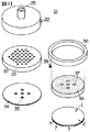
図8はパターン付きウエハ研磨装置の実施形態2を示すヘッドの一部省略分解斜視図である。図9はその作用を説明するための説明図である。
【0050】
図8に示されているヘッド21Aが図1および図2に示されたヘッド21と異なる点は、ワーク周辺部の研磨速度が速くなるのを抑制するためのバッキングパッド(以下、研磨速度分布制御パッドという。)36Aが使用されている点である。すなわち、研磨速度分布制御パッド36Aの周辺部には、平均圧縮弾性率Eを部分的に調整するための調整孔40が複数個開設されている。研磨速度分布制御パッド36Aの周辺部における平均圧縮弾性率Eは、中央部のそれよりも調整孔40が開設された分だけ低下している。研磨速度分布制御パッド36Aの周辺部における平均圧縮弾性率Eは、調整孔40の大きさおよび配置間隔の選択によって任意に調整することができる。
【0051】
次に、研磨速度分布制御パッド36Aの作用を図9によって説明する。ところで、パターン付きウエハ研磨装置においてワークが自転されていると、ワークの周辺部における摺動速度は中心部の摺動速度よりも速くなるため、被研磨面の研磨速度は周辺部において速くなる。図9(a)はワーク1であるパターン付きウエハのペレット9の配置を示している。図9(a)において、斜線を付して示した周辺部のペレット9aは研磨速度の速い周辺部領域9bに部分的に懸かるため、ペレット9a内の研磨量が不均一になる。その結果、周辺部のペレット9aのパターニングは不完全になり、周辺部のペレット9aは不良品になる。被研磨面の周辺部の研磨速度が速くなるのは、前述したパターン付きウエハ研磨装置10においても同様である。これは図6(b)の研磨速度分布を示すグラフによっても理解することができる。
【0052】
本実施形態2においては、図1および図2に示されたバッキングパッド36の代わりに、図8に示されているように研磨速度分布制御パッド36Aが使用されているため、被研磨面の周辺部の研磨速度が速くなる現象が防止される。研磨速度分布制御パッド36Aの周辺部の平均圧縮弾性率Eは調整孔40の開設によって低下されているため、研磨速度分布制御パッド36Aの周辺部のワーク1に対する弾発力は弱くなる。研磨速度分布制御パッド36Aの弾発力が弱くなった分だけ、被研磨面7の周辺部が研磨速度分布制御パッド36Aの弾発力によって研磨材面15に押し付けられる力が弱くなるため、被研磨面7が研磨材面15によって化学的機械研磨される研磨速度は抑制される。その結果、図9(a)に示された周辺部のペレット9aの研磨量は均一になるため、周辺部のペレット9aのパターニングは完全になり、周辺部のペレット9aは良品になる。つまり、ワーク一枚当たりの製造歩留りが向上し、ペレットの実効取得数が増加する。
【0053】
図9(b)は研磨速度分布制御パッドの周辺部における平均圧縮弾性率が研磨速度均一性に及ぼす影響を示すグラフである。このグラフは、直径8インチの研磨速度分布制御パッド36Aの外周から5mmの範囲に直径1mmの調整孔40を個数を変更して開けることにより、平均圧縮弾性率が順次変更調整されて得られた。図9(b)において、横軸には平均圧縮弾性率Eが取られている。ここで、平均圧縮弾性率Eは研磨速度分布制御パッドの初期弾性率に対する周辺部の平均圧縮弾性率の百分率によって表されている。縦軸には研磨速度均一性rが取られている。ここで、研磨速度均一性rは被研磨面における中心部の平均研磨速度に対する周辺部の平均研磨速度の比によって表されている。
【0054】
図9(b)により次のことが究明された。研磨速度分布制御パッドの外周部の平均圧縮弾性率Eを初期弾性率の約75%に設定することにより、被研磨面の外周部における研磨速度均一性rを最小に抑制することができる。なお、研磨速度分布制御パッドの周辺部における平均圧縮弾性率Eの最適値は、ワークの大きさや厚さ、被研磨面の性質や硬さ、機械的圧力、エア圧力等の化学的機械研磨の諸条件に応じて変わる。研磨速度分布制御パッドの平均圧縮弾性率Eは研磨速度分布制御パッドに調整孔を開けることによって調整するに限らず、研磨速度分布制御パッドの外周部を削除する方法や、外周部に切り込みを入れる方法等によっても調整することができる。
【0055】
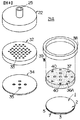
図10はパターン付きウエハ研磨装置の実施形態3を示す一部省略一部切断正面図である。
【0056】
本実施形態3が前記実施形態1と異なる点は、バッキングパッドが省略された点である。ワーク1は弾性膜34に直接接触した状態で、加圧板32によって機械的に押され、かつ、弾性膜34に加わるエア圧力による作用力によって付勢される。したがって、ワーク1の被研磨面は前記実施形態1と同様な作用により全体にわたって均一に化学的機械研磨される。
【0057】
図11はパターン付きウエハ研磨装置の実施形態4を示す一部省略一部切断正面図である。
【0058】
本実施形態4が前記実施形態1と異なる点は、真空吸着のための弾性膜の透孔およびバッキングパッドの透孔が省略され、負圧供給路が省略された点である。省略された構成要素はワーク1の真空吸着保持に使用されるため、化学的機械研磨における被研磨面の均一性の向上効果には影響しない。したがって、前記実施形態1と同様な作用効果が奏される。
【0059】
以上本発明者によってなされた発明を実施形態に基づき具体的に説明したが、本発明は前記実施形態に限定されるものではなく、その要旨を逸脱しない範囲で種々変更可能であることはいうまでもない。
【0060】
加圧板に開設する通気孔は複数本に限らず、1本でもよい。また、通気路は加圧板の上下空間を連通させればよいため、通気路は加圧板を多孔質剛性板で形成することによっても構成することができる。
【0061】
加圧板および弾性膜のヘッド本体への固定手段は締結手段に限らず、接着手段等を使用してもよい。
【0062】
弾性膜を介してワークを付勢する気体としてはエアを使用するに限らず、窒素等の気体を使用してもよい。
【0063】
ヘッドを上側に研磨工具を下側に配置するに限らず、ヘッドを下側に研磨工具を上側に配置してもよい。また、ヘッド側を下降させるように構成するに限らず、研磨工具側を上昇させるように構成してもよい。さらに、ヘッドと研磨工具とは上下方向に不動とし、ワークの被研磨面と研磨工具の研磨材面とを相対的に水平方向に移動させて単に擦り合わせるように構成してもよい。
【0064】
バッキングパッドはゴムまたは樹脂、発泡樹脂によって構成するに限らず、フェルトやガラスウール等の適度な弾力性を有する材料によって構成することができる。
【0065】
【発明の効果】
本願において開示される発明のうち代表的なものによって得られる効果を簡単に説明すれば、次の通りである。
【0066】
化学的機械研磨時にワークに作用する不規則で複雑な歪みに自己整合的に対応してワークに対する押し力を補正することにより、ワークの被研磨面を全体にわたって均一に、しかも、高い均一精度をもって化学的機械研磨することができるため、高精度のパターニングを確保することができる。その結果、超微細で高集積度の半導体装置を製造する方法を提供することができる。
【図面の簡単な説明】
【図1】本発明の一実施形態である半導体装置の製造方法に使用されるパターン付きウエハ研磨装置を示す一部省略一部切断正面図である。
【図2】そのヘッドを示す一部省略分解斜視図である。
【図3】ワークを示しており、(a)は平面図、(b)は拡大部分断面図である。
【図4】本発明の一実施形態である半導体装置の製造方法を説明するための各拡大部分断面図を示しており、(a)は第1配線形成工程、(b)は第2絶縁膜形成工程、(c)は平坦化工程、(d)はホール形成工程、(e)は第2配線形成工程を示している。
【図5】加圧板による機械的な押し力とエア圧力による作用力との関係が化学的機械研磨の研磨量均一性および平均研磨速度に及ぼす影響を示すグラフである。
【図6】研磨速度分布を示すグラフであり、(a)は図5のaによって示された圧力比の条件で化学的機械研磨した場合のグラフ、(b)は図5のbによって示された圧力比Sの条件で化学的機械研磨した場合のグラフ、(c)は図5のcによって示された圧力比Sの条件で化学的機械研磨した場合のグラフを示している。
【図7】本発明の他の実施形態である半導体装置の製造方法をSTI法に適用した場合を示す各拡大部分断面図であり、(a)は素子分離溝形成工程、(b)は絶縁膜形成工程、(c)は絶縁膜除去工程、(d)は絶縁膜除去が不均一になった状態の絶縁膜除去工程、(e)はマスク除去工程、(f)はゲート酸化膜形成工程、(g)は不純物拡散およびゲート電極形成工程を示している。
【図8】パターン付きウエハ研磨装置の実施形態2を示すヘッドの一部省略分解斜視図である。
【図9】その作用を説明するための説明図であり、(a)はパターン付きウエハのペレットの配置を示す平面図、(b)は研磨速度分布制御パッドの周辺部における平均圧縮弾性率が研磨速度均一性に及ぼす影響を示すグラフである。
【図10】パターン付きウエハ研磨装置の実施形態3を示す一部省略一部切断正面図である。
【図11】パターン付きウエハ研磨装置の実施形態4を示す一部省略一部切断正面図である。
【符合の説明】
1…ワーク(半導体ウエハ)、2…サブストレート(ウエハ)、3…オリエンテーションフラット(オリフラ)、4…配線、4a…第1配線、4b…第2配線、4c…スルーホール、4d…スルーホール導体、5…層間絶縁膜(絶縁膜)、5a…第1絶縁膜、5b…第2絶縁膜、6…凹凸部、7…被研磨面、8…裏側面、9…ペレット、9a…周辺部のペレット、9b…研磨速度の速い周辺部領域、10…パターン付きウエハ研磨装置(CMP)、11…研磨工具、12…ベースプレート、13…回転軸、14…研磨クロス、15…研磨材面、16…スラリ供給ノズル、17…スラリ、21…ヘッド、22…ヘッド本体、23…保持穴、24…通気口(気体流通口)、25…通気路(流体圧供給路)、26…エアポンプ、27…エア(気体)、28…正圧供給路、29…真空ポンプ、30…負圧供給路、31…切換弁、32…加圧板、33…通気孔(通気路)、34…弾性膜、35…透孔、36…バッキングパッド、36A…研磨速度分布制御パッド、37…透孔、38…ガイドリング、39…ボルト、40…調整孔、41…マスク、42…素子分離溝、43…絶縁膜、43a…研磨過多部、43b…研磨不足部、44…絶縁物充填部、45…絶縁膜の表面(被研磨面)、46…凹凸部、47…素子分離部、48…素子形成部、49…ゲート酸化膜、50…不純物拡散層、51…ゲート電極。[0001]
TECHNICAL FIELD OF THE INVENTION
The present invention relates to a technique for manufacturing a semiconductor device, and particularly to a technique for performing chemical mechanical polishing on a main surface on a patterning side of a patterned semiconductor wafer (hereinafter, referred to as a wafer).
[0002]
[Prior art]
Recently, there has been proposed a method of manufacturing a semiconductor device in which unevenness on a patterning-side main surface of a patterned wafer (hereinafter, referred to as a patterned wafer) is planarized by chemical mechanical polishing. The technique of flattening the unevenness of the patterned main surface of a patterned wafer by chemical mechanical polishing has the following problems as compared with the technique of flattening the unevenness of the main surface of the wafer before patterning by chemical mechanical polishing. There are points. The first problem is that the amount of polishing (corresponding to the amount removed by processing) is extremely small. For example, while the polishing amount of the wafer before patterning is several tens of μm, the polishing amount of the patterned wafer is about 0.5 μm. The second problem is that the flatness of the main surface on the patterning side, which is the surface to be polished of the patterned wafer, is much more ambiguous than that of the surface to be polished of the wafer before patterning. In consideration of these problems, it is difficult to uniformly perform chemical mechanical polishing on the entire surface of the patterned wafer of the patterned wafer.
[0003]
Japanese Patent Application Laid-Open Nos. 5-74749, 6-15563, and 5-69310 disclose Japanese Patent Application Laid-Open Nos. Hei 5-74749, Hei 6-15563, and Japanese Patent Application Laid-Open Nos. Hei 5-74749, which describe a chemical mechanical polishing technique for a patterned wafer which overcomes this difficulty. No. Gazette. All of the techniques disclosed in these examples are based on the principle that the polished surface of the patterning side main surface is uniformly rubbed over the entire surface of the abrasive material by pressing the patterned wafer with an elastic body sealed with a pressure fluid. And
[0004]
[Problems to be solved by the invention]
However, in the conventional chemical mechanical polishing technique for a patterned wafer utilizing the above-mentioned principle, there is a problem that the accuracy of 0.1 μm or less cannot be secured for the uniformity of the polishing amount (described later). , Was made clear by the present inventors.
[0005]
An object of the present invention is to provide a semiconductor device manufacturing technique capable of uniformly polishing the surface to be polished of a patterned wafer with high accuracy.
[0006]
The above and other objects and novel features of the present invention will become apparent from the description of the present specification and the accompanying drawings.
[0007]
[Means for Solving the Problems]
The outline of a typical invention disclosed in the present application will be described as follows.
[0008]
That is, in performing the chemical mechanical polishing of the surface of the patterning side main surface of the semiconductor wafer, the pressure plate having the ventilation path is held by the wafer holding head body having the ventilation port, and the pressure plate has the ventilation port side. A wafer holding head having an elastic film applied to the opposite main surface is prepared in advance. The semiconductor wafer to be subjected to chemical mechanical polishing is held by the wafer holding head in a state where a main surface opposite to the main surface on the patterning side is applied to the elastic film. The semiconductor wafer thus held is rubbed against a polishing cloth with the surface of the patterning side main surface in a state where the semiconductor wafer held by the pressure plate is pressed by the action force of the pressure of the gas supplied to the vent while being mechanically pressed by the pressure plate. Chemical mechanical polishing.
[0009]
According to the above-described means, the surface to be polished is pressed against the polishing cloth by the pressing force of the pressure plate and chemically and mechanically polished. At this time, an irregular and complicated strain force acting on the surface to be polished is generated by gas. Since the correction is made in a self-aligned manner by the acting force of the pressure, the polishing amount of the surface to be polished becomes uniform over the entire surface.
[0010]
BEST MODE FOR CARRYING OUT THE INVENTION
FIG. 1 is a partially cutaway front view showing a partially polished wafer polishing apparatus used in a method of manufacturing a semiconductor device according to an embodiment of the present invention. FIG. 2 is a partially omitted exploded perspective view showing the head. FIG. 3 et seq. Are explanatory diagrams illustrating a method for manufacturing a semiconductor device according to an embodiment of the present invention.
[0011]
In the present embodiment, the method for manufacturing a semiconductor device according to the present invention uses the patterned wafer polishing apparatus shown in FIG. The patterned
[0012]
Here, a patterned wafer (hereinafter, referred to as a workpiece) 1 shown in FIG. 3 which is a target of the method of manufacturing a semiconductor device according to the present invention and is a workpiece of the patterned
[0013]
The patterned
[0014]
The
[0015]
A
[0016]
An
[0017]
A disc-shaped
[0018]
A circular ring-shaped
[0019]
The
[0020]
Next, a method of manufacturing a semiconductor device according to an embodiment of the present invention will be described with reference to FIG.
[0021]
As shown in FIG. 4A, a first insulating film 5a in a multilayer wiring is formed on the front surface of the
[0022]
Next, as shown in FIG. 4B, a
[0023]
The
[0024]
Subsequently, the polishing tool 11 and the
[0025]
While the
[0026]
Since the surface of the second
[0027]
After the chemical mechanical polishing of the set polishing amount is completed, the surface of the second
[0028]
The
[0029]
Subsequently, in a second wiring forming step, a
[0030]
Thereafter, the above-described insulating film forming step, flattening step, hole forming step, and wiring forming step are repeated to form the multilayer wiring shown in FIG. 3B. At this time, the insulating film and the wiring of the layer formed in the previous step correspond to the insulating film and the wiring of the lower layer in the next step. The holes are not limited to through holes, but include contact holes. Further, the hole is not limited to connecting the wiring of the first layer to the wiring of the second layer, and may connect the wiring of the first layer to the wiring of the third layer or the fourth layer.
[0031]
Here, the influence of the relationship between the mechanical pressing force by the
[0032]
FIG. 5 is a graph showing the effect of the relationship between the mechanical pressing force of the
[0033]
The following has been determined by FIG. The polishing amount uniformity D is improved when the pressure ratio S is in the range of about 0.7 to 1.5. The average polishing rate R increases until S = 1, and tends to be saturated when S ≧ 1. The reason why the average polishing rate R tends to be saturated when S ≧ 1 is that the polishing amount uniformity is reduced. The reason why the uniformity of the polishing amount is reduced is that when the pressure ratio S becomes excessively large, the
[0034]
Based on the above findings, the present inventors considered the following. The uniformity of the polishing amount by the chemical mechanical polishing is almost controlled by the mechanical pressing force of the
[0035]
By the way, the reason that the conventional technique of chemically and mechanically polishing a patterned wafer with an elastic body in which the pressure fluid is sealed cannot secure the accuracy of 0.1 μm or less for the uniformity of the polishing amount is based on the above consideration. It is estimated that: The state in which the elastic body sealed with the pressure fluid presses the patterned wafer is the same as the state in which the
[0036]
FIG. 6 is a graph showing a polishing rate distribution in the radial direction of a silicon wafer. In FIG. 6, the horizontal axis represents the position P of the silicon wafer, and the vertical axis represents the polishing speed V. FIG. 6A is a graph showing a case where chemical mechanical polishing is performed under the condition of the pressure ratio S shown in FIG. 5A. FIG. 6B shows a graph in the case where chemical mechanical polishing is performed under the condition of the pressure ratio S shown by b in FIG. FIG. 6C shows a graph in the case of performing chemical mechanical polishing under the condition of the pressure ratio S shown by c in FIG.
[0037]
According to FIG. 6A, it can be seen that the silicon oxide film was polished earlier in the peripheral portion than in the central portion of the wafer. FIG. 6B shows that the silicon oxide film was entirely polished from the center to the periphery of the wafer. According to FIG. 6C, it can be seen that the silicon oxide film is polished more slowly at the central portion than at the peripheral portion of the wafer, and its distribution is complicated. As a result, when the chemical mechanical polishing is performed under the condition that the pressure ratio S is set to 1, the polishing rate distribution becomes uniform throughout.
[0038]
According to the method for manufacturing a semiconductor device according to the present embodiment, when flattening the unevenness formed by the lower wiring on the surface of the upper insulating film by chemical mechanical polishing, the upper insulating film which is the surface to be polished is removed. Since the entire surface can be flattened uniformly and with high precision uniformity, insufficient polishing or excessive polishing can be prevented from locally occurring. As a result, miniaturization and higher density of the multilayer wiring of the semiconductor device can be promoted.
[0039]
Next, a method of manufacturing a semiconductor device according to a second embodiment of the present invention will be described with reference to FIG. 7 by taking as an example a case where a shallow trench isolation (hereinafter, referred to as STI) method is applied. Will be explained.
[0040]
When the STI method is performed, as shown in FIG. 3 N 4 It is dug by a dry etching method using a
[0041]
Next, as shown in FIG. 2 An insulating
[0042]
The
[0043]
When the
[0044]
The
[0045]
Thereafter, a
[0046]
Next, as shown in FIG. 7G, an
[0047]
According to the method of manufacturing the semiconductor device according to the second embodiment described above, when the element isolation portion is formed by the chemical mechanical polishing by the STI method, the surface layer portion of the insulating film for forming the element isolation portion is formed. Since it can be completely removed with high uniformity over the entire surface, insufficient polishing or excessive polishing of the insulating film can be prevented from locally occurring. As a result, the accuracy of the element isolation portion, the gate oxide film, the impurity diffusion layer, and the gate electrode by the STI method can be improved, and the miniaturization and higher density of the semiconductor device can be further promoted.
[0048]
The
[0049]
FIG. 8 is a partially omitted exploded perspective view of a head showing a second embodiment of the patterned wafer polishing apparatus. FIG. 9 is an explanatory diagram for explaining the operation.
[0050]
The
[0051]
Next, the operation of the polishing rate
[0052]
In the second embodiment, since the polishing rate
[0053]
FIG. 9B is a graph showing the effect of the average compressive modulus at the periphery of the polishing rate distribution control pad on polishing rate uniformity. This graph was obtained by changing and adjusting the average compression elastic modulus sequentially by changing the number of adjustment holes 40 having a diameter of 1 mm in a range of 5 mm from the outer periphery of the polishing rate
[0054]
The following was determined from FIG. 9B. By setting the average compression modulus E of the outer peripheral portion of the polishing rate distribution control pad to about 75% of the initial elastic modulus, the polishing rate uniformity r at the outer peripheral portion of the surface to be polished can be minimized. The optimum value of the average compressive modulus E in the peripheral portion of the polishing rate distribution control pad is determined by the size and thickness of the workpiece, the properties and hardness of the surface to be polished, the mechanical pressure, the air pressure, etc. It changes according to various conditions. The average compression elastic modulus E of the polishing rate distribution control pad is not limited to be adjusted by forming an adjustment hole in the polishing rate distribution control pad, but may be a method of removing the outer peripheral portion of the polishing speed distribution control pad or making a cut in the outer peripheral portion. It can also be adjusted by a method or the like.
[0055]
FIG. 10 is a partially omitted partially cut front view showing a third embodiment of the patterned wafer polishing apparatus.
[0056]
The third embodiment differs from the first embodiment in that the backing pad is omitted. The
[0057]
FIG. 11 is a partially omitted partially cut front view showing a fourth embodiment of the patterned wafer polishing apparatus.
[0058]
The fourth embodiment differs from the first embodiment in that the through-hole of the elastic film for vacuum suction and the through-hole of the backing pad are omitted, and the negative pressure supply path is omitted. Since the omitted components are used for holding the
[0059]
Although the invention made by the inventor has been specifically described based on the embodiment, the present invention is not limited to the embodiment, and various changes can be made without departing from the gist of the invention. Nor.
[0060]
The number of air holes formed in the pressure plate is not limited to a plurality but may be one. In addition, since the ventilation path may communicate the upper and lower spaces of the pressure plate, the ventilation path can also be configured by forming the pressure plate with a porous rigid plate.
[0061]
The means for fixing the pressure plate and the elastic film to the head main body is not limited to the fastening means, and an adhesive means or the like may be used.
[0062]
The gas for urging the workpiece through the elastic film is not limited to air, but may be a gas such as nitrogen.
[0063]
The head is not limited to disposing the polishing tool on the upper side, and the polishing tool may be disposed on the upper side on the lower side. Further, the present invention is not limited to the configuration in which the head side is lowered, but may be configured to raise the polishing tool side. Further, the head and the polishing tool may be vertically immovable, and the surface to be polished of the workpiece and the abrasive material surface of the polishing tool may be relatively horizontally moved and simply rubbed.
[0064]
The backing pad is not limited to being made of rubber, resin, or foamed resin, but may be made of a material having appropriate elasticity such as felt or glass wool.
[0065]
【The invention's effect】
The effect obtained by the representative one of the inventions disclosed in the present application will be briefly described as follows.
[0066]
By correcting the pressing force against the work in a self-aligning manner to respond to the irregular and complicated strain acting on the work during chemical mechanical polishing, the work surface to be polished can be made uniform over the entire surface with high uniform accuracy. Since chemical mechanical polishing can be performed, high-precision patterning can be ensured. As a result, it is possible to provide a method for manufacturing an ultrafine and highly integrated semiconductor device.
[Brief description of the drawings]
FIG. 1 is a partially cutaway front view showing a partially polished wafer polishing apparatus used in a method of manufacturing a semiconductor device according to an embodiment of the present invention.
FIG. 2 is a partially omitted exploded perspective view showing the head.
3A and 3B show a workpiece, wherein FIG. 3A is a plan view and FIG. 3B is an enlarged partial cross-sectional view.
4A and 4B are enlarged partial cross-sectional views illustrating a method for manufacturing a semiconductor device according to an embodiment of the present invention, wherein FIG. 4A is a first wiring forming step, and FIG. 4B is a second insulating film; (C) shows a flattening step, (d) shows a hole forming step, and (e) shows a second wiring forming step.
FIG. 5 is a graph showing an effect of a relationship between a mechanical pressing force by a pressure plate and an acting force by an air pressure on a polishing amount uniformity and an average polishing speed in chemical mechanical polishing.
6 is a graph showing a polishing rate distribution, in which (a) is a graph in the case of performing chemical mechanical polishing under the condition of the pressure ratio shown by a in FIG. 5, and (b) is shown by b in FIG. FIG. 5C shows a graph when the chemical mechanical polishing is performed under the condition of the pressure ratio S shown in FIG. 5C, and FIG. 5C shows a graph when the chemical mechanical polishing is performed under the condition of the pressure ratio S shown in FIG.
FIGS. 7A and 7B are enlarged partial cross-sectional views showing a case where a method of manufacturing a semiconductor device according to another embodiment of the present invention is applied to an STI method, wherein FIG. 7A is an element isolation groove forming step, and FIG. A film forming step, (c) an insulating film removing step, (d) an insulating film removing step in a state where the insulating film is not uniformly removed, (e) a mask removing step, and (f) a gate oxide film forming step. , (G) show steps of impurity diffusion and gate electrode formation.
FIG. 8 is a partially omitted exploded perspective view of a head showing a second embodiment of the patterned wafer polishing apparatus;
FIGS. 9A and 9B are explanatory diagrams for explaining the operation, in which FIG. 9A is a plan view showing an arrangement of pellets on a patterned wafer, and FIG. 4 is a graph showing the effect on polishing rate uniformity.
FIG. 10 is a partially omitted partially cut front view showing a third embodiment of the patterned wafer polishing apparatus;
FIG. 11 is a partially cutaway front view of a partially polished wafer polishing apparatus according to a fourth embodiment of the present invention.
[Description of sign]
DESCRIPTION OF
Claims (7)
通気口を有するウエハ保持ヘッド本体に通気路を有する加圧板を保持し、かつ、前記加圧板の前記通気口側と反対側の主面に前記加圧板の通気路を塞ぐように弾性膜が当てがわれたウエハ保持ヘッドを予め用意し、前記半導体ウエハの前記パターニング側主面と反対側の主面を前記ウエハ保持ヘッドの前記弾性膜に当接させた状態で保持し、前記半導体ウエハの前記パターニング側主面と反対側の主面を前記加圧板によって機械的に押しながら、同時に前記通気口に供給された気体圧力を前記通気路を通して前記弾性膜に加えることにより、機械的圧力と気体圧力との両方を前記反対側の主面に加えながら、前記パターニング側主面の表面を研磨クロスに擦り付けて平坦化することを特徴とする半導体装置の製造方法。 The method of manufacturing a semiconductor device of more flattening the chemical mechanical polishing the surface of the patterning side main surface of the semiconductor wafer having a patterned uneven,
Holding the pressure plate having a vent passage to the wafer holding head body having a vent, and wherein the elastic film so as to close the air passage of the pressure plate against the opposite side of the main surface and the vent side of the pressure plate previously prepared wafer holding head We have, to hold the patterning side main surface opposite the main surface of the semiconductor wafer in a state in which the abutted against the elastic membrane of the wafer holding head, of the semiconductor wafer while mechanically pressing the main surface opposite to the patterned side main surface by the pressure plate, by adding the supplied gas pressure to the elastic film through the ventilation channel simultaneously the vent, and mechanical pressure A method of manufacturing a semiconductor device , wherein a surface of the main surface on the patterning side is rubbed against a polishing cloth to flatten while applying both gas pressure and the main surface on the opposite side .
(a) 半導体ウエハに形成された第1絶縁膜の上に第1層配線を形成する第1層配線形成工程、
(b) 前記第1絶縁膜および前記第1層配線の上に第2絶縁膜を形成する第2絶縁膜形成工程、
(c) 通気口を有するウエハ保持ヘッド本体に通気路を有する加圧板を保持し、かつ、前記加圧板の前記通気口側と反対側の主面に前記加圧板の通気路を塞ぐように弾性膜が当てがわれたウエハ保持ヘッドを予め用意し、前記半導体ウエハの前記パターニング側主面と反対側の主面を前記ウエハ保持ヘッドの前記弾性膜に当接させた状態で保持し、前記半導体ウエハの前記パターニング側主面と反対側の主面を前記加圧板によって機械的に押しながら、同時に前記通気口に供給された気体圧力を前記通気路を通して前記弾性膜に加えることにより、機械的圧力と気体圧力との両方を前記反対側の主面に加えながら、前記第2絶縁膜の表面を研磨クロスに擦り付けて平坦化する平坦化工程、
(d)平坦化された第2絶縁膜にスルーホールまたはコンタクトホールを形成する接続孔形成工程、
(e) 前記接続孔が形成された前記第2絶縁膜の上に第2配線層を形成する第2配線層形成工程、
を含むことを特徴とする半導体装置の製造方法。In a method of manufacturing a semiconductor device for flattening a surface having unevenness of a multilayer wiring structure formed on a semiconductor wafer ,
(A) a first- layer wiring forming step of forming a first- layer wiring on a first insulating film formed on a semiconductor wafer;
(B) a second insulating film forming step of forming a second insulating film on the first insulating film and the first layer wiring;
Holding the pressure plate having a vent passage to the wafer holding head body (c) having a ventilation opening, and an elastic so as to close the air passage of the pressure plate opposite the main face and the vent side of the pressure plate film prepared against previously wafer holding head we will hold the patterned side main surface opposite the main surface of the semiconductor wafer in a state in which the abutted against the elastic membrane of the wafer holding head, wherein while mechanically pressing the opposite side of the main surface and the patterning side main surface of the semiconductor wafer by the pressure plate, by adding the supplied gas pressure to the elastic film through the ventilation channel simultaneously the vent, mechanical pressure and while both the gas pressure to the main surface of the opposite side, flattening step you planarize rubbing the surface of the second insulating film to the polishing cloth,
(D) that form a through hole or contact hole in the second insulating film is flattened connection hole forming step,
(E) second wiring layer formation step you forming a second wiring layer over the said connection hole is formed second insulating film,
A method for manufacturing a semiconductor device, comprising:
(a) 前記サブストレート主面上に素子分離用の溝を形成する素子分離溝の形成工程、
(b) 前記サブストレート上に形成された素子分離溝の内部および前記素子分離溝の外部の前記サブストレート主面上に絶縁膜を被着して前記素子分離溝内に絶縁物充填部を形成する絶縁膜被着工程、
(c) 通気口を有するウエハ保持ヘッド本体に通気路を有する加圧板を保持し、かつ、前記加圧板の前記通気口側と反対側の主面に前記加圧板の通気路を塞ぐように弾性膜が当てがわれたウエハ保持ヘッドを予め用意し、前記半導体ウエハの前記パターニング側主面と反対側の主面を前記ウエハ保持ヘッドの前記弾性膜に当接させた状態で保持し、前記半導体ウエハの前記パターニング側主面と反対側の主面を前記加圧板によって機械的に押しながら、同時に前記通気口に供給された気体圧力を前記通気路を通して前記弾性膜に加えることにより、機械的圧力と気体圧力との両方を前記反対側の主面に加えながら、前記絶縁膜の表面を研磨クロスに擦り付けて化学的機械研磨により平坦化することにより、前記絶縁物充填部によって素子分離部を形成する素子分離部形成工程、
(d) 前記サブストレート上主面における前記素子分離部に囲まれた素子形成部の上にゲートを形成するゲート形成工程、
を含むことを特徴とする半導体装置の製造方法。 The method of manufacturing a semiconductor device for forming a semiconductor element on a substrate of a semiconductor wafer,
(A) said step of forming the element isolation grooves forming a trench for isolation in the substrate on a main surface,
(B) forming an insulator filling unit to the substrate on the formed element isolation trench in the inside and the device isolation trench of the outside of the insulating film to the substrate on the main surface by adhering the element isolation trench insulating film deposition process you,
Holding the pressure plate having a vent passage to the wafer holding head body (c) having a ventilation opening, and an elastic so as to close the air passage of the pressure plate opposite the main face and the vent side of the pressure plate film prepared against previously wafer holding head we will hold the patterned side main surface opposite the main surface of the semiconductor wafer in a state in which the abutted against the elastic membrane of the wafer holding head, wherein while mechanically pressing the opposite side of the main surface and the patterning side main surface of the semiconductor wafer by the pressure plate, by adding the supplied gas pressure to the elastic film through the ventilation channel simultaneously the vent, mechanical By applying both mechanical pressure and gas pressure to the main surface on the opposite side, the surface of the insulating film is rubbed against a polishing cloth and flattened by chemical mechanical polishing, thereby isolating elements by the insulating filled portion. Element isolation portion formation step that form a part,
(D) a gate formation step you forming a gate over the isolation portion surrounded by the element forming portion of the substrate on a main surface,
A method for manufacturing a semiconductor device, comprising:
(a) 半導体ウエハ上に第1絶縁膜を形成する第1絶縁膜形成工程、
(b) 前記第1絶縁膜にリセスを形成するように前記第1絶縁膜を選択的にエッチングすることにより前記第1絶縁膜に第1のパターンを形成する第1パターン形成工程、
(c) 前記第1パターンのリセス部分および前記リセスの外側の前記第1絶縁膜上に第1の導電膜を形成する工程、
(d) 通気口を有するウエハ保持ヘッド本体に通気路を有する加圧板を保持し、かつ、前記加圧板の前記通気口側と反対側の主面に前記加圧板の通気路を塞ぐように弾性膜が当てがわれたウエハ保持ヘッドを予め用意し、前記半導体ウエハの前記パターニング側主面と反対側の主面を前記ウエハ保持ヘッドの前記弾性膜に当接させた状態で保持し、前記半導体ウエハの前記パターニング側主面と反対側の主面を前記加圧板によって機械的に押しながら、同時に前記通気口に供給された気体圧力を前記通気路を通して前記弾性膜に加えることにより、機械的圧力と気体圧力との両方を前記反対側の主面に加えながら、前記第1の導電膜の表面を研磨クロスに擦り付けて平坦化することにより、前記リセス内に前記第1の導電膜を残す平坦化工程、
を含むことを特徴とする半導体装置の製造方法。 Te manufacturing method odor of a semiconductor device for embedding wiring formed on the semiconductor wafer,
(A) the first insulating film forming step you forming a first insulating film on a semiconductor wafer,
(B) a first pattern forming step of forming a first pattern in the first insulating film by selectively etching the first insulating film so as to form a recess in the first insulating film ;
(C) forming a first conductive film on the recessed portion of the first pattern and on the first insulating film outside the recess ;
(D) holding the pressure plate having a vent passage to the wafer holding head body having a vent, and elastic so as to close the air passage of the pressure plate opposite the main face and the vent side of the pressure plate film prepared against previously wafer holding head we will hold the patterned side main surface opposite the main surface of the semiconductor wafer in a state in which the abutted against the elastic membrane of the wafer holding head, wherein while mechanically pressing the opposite side of the main surface and the patterning side main surface of the semiconductor wafer by the pressure plate, by adding the supplied gas pressure to the elastic film through the ventilation channel simultaneously the vent, mechanical The surface of the first conductive film is rubbed against a polishing cloth and flattened while applying both the mechanical pressure and the gas pressure to the main surface on the opposite side, thereby placing the first conductive film in the recess. Flattening process to leave ,
A method for manufacturing a semiconductor device, comprising:
Priority Applications (4)
| Application Number | Priority Date | Filing Date | Title |
|---|---|---|---|
| JP12913596A JP3552845B2 (en) | 1996-04-25 | 1996-04-25 | Method for manufacturing semiconductor device |
| TW086104361A TW340962B (en) | 1996-04-25 | 1997-04-07 | Manufacturing method of a semiconductor IC |
| KR1019970015179A KR970072156A (en) | 1996-04-25 | 1997-04-23 | Manufacturing method of semiconductor integrated circuit device |
| US08/845,398 US6147001A (en) | 1996-04-25 | 1997-04-24 | Method of manufacturing semiconductor integrated circuit device |
Applications Claiming Priority (1)
| Application Number | Priority Date | Filing Date | Title |
|---|---|---|---|
| JP12913596A JP3552845B2 (en) | 1996-04-25 | 1996-04-25 | Method for manufacturing semiconductor device |
Publications (2)
| Publication Number | Publication Date |
|---|---|
| JPH09293699A JPH09293699A (en) | 1997-11-11 |
| JP3552845B2 true JP3552845B2 (en) | 2004-08-11 |
Family
ID=15001985
Family Applications (1)
| Application Number | Title | Priority Date | Filing Date |
|---|---|---|---|
| JP12913596A Expired - Fee Related JP3552845B2 (en) | 1996-04-25 | 1996-04-25 | Method for manufacturing semiconductor device |
Country Status (4)
| Country | Link |
|---|---|
| US (1) | US6147001A (en) |
| JP (1) | JP3552845B2 (en) |
| KR (1) | KR970072156A (en) |
| TW (1) | TW340962B (en) |
Families Citing this family (10)
| Publication number | Priority date | Publication date | Assignee | Title |
|---|---|---|---|---|
| US5925576A (en) * | 1998-08-19 | 1999-07-20 | Promos Technologies, Inc. | Method and apparatus for controlling backside pressure during chemical mechanical polishing |
| JP3409759B2 (en) * | 1999-12-09 | 2003-05-26 | カシオ計算機株式会社 | Manufacturing method of semiconductor device |
| KR100811172B1 (en) * | 2000-05-12 | 2008-03-10 | 멀티-플레이너 테크놀로지즈 인코포레이티드 | Pneumatic diaphragm head having an independent retaining ring and multi-region pressure control, and method to use the same |
| JP4959901B2 (en) * | 2000-05-27 | 2012-06-27 | ローム アンド ハース エレクトロニック マテリアルズ シーエムピー ホウルディングス インコーポレイテッド | Polishing pad with groove for chemical mechanical planarization |
| JP2007129115A (en) * | 2005-11-07 | 2007-05-24 | Fuji Electric Holdings Co Ltd | Manufacturing method for semiconductor device |
| JP2009158749A (en) * | 2007-12-27 | 2009-07-16 | Ricoh Co Ltd | Chemical mechanical polishing method and chemical mechanical polishing apparatus |
| JP5847519B2 (en) * | 2011-09-29 | 2016-01-20 | 京セラクリスタルデバイス株式会社 | Wafer bonding equipment |
| CN104870341B (en) * | 2012-10-19 | 2018-02-06 | 陶氏环球技术有限责任公司 | For lifted and moved it is shapable and/or can avalanche part devices, systems, and methods |
| US10315286B2 (en) | 2016-06-14 | 2019-06-11 | Axus Technologi, Llc | Chemical mechanical planarization carrier system |
| KR102641195B1 (en) * | 2021-11-26 | 2024-02-27 | (주)나노랩스 | Electrospinning Device Capable of Recovering Different Types of Spinning Liquids |
Family Cites Families (8)
| Publication number | Priority date | Publication date | Assignee | Title |
|---|---|---|---|---|
| JPH0569310A (en) * | 1991-04-23 | 1993-03-23 | Mitsubishi Materials Corp | Device for grinding mirror surface of wafer |
| JP3233664B2 (en) * | 1991-09-13 | 2001-11-26 | 土肥 俊郎 | Method and apparatus for planarization polishing of wafer with device |
| JP3218572B2 (en) * | 1992-07-01 | 2001-10-15 | 不二越機械工業株式会社 | Polishing plate for wafer pressing |
| US5604158A (en) * | 1993-03-31 | 1997-02-18 | Intel Corporation | Integrated tungsten/tungsten silicide plug process |
| JP2891068B2 (en) * | 1993-10-18 | 1999-05-17 | 信越半導体株式会社 | Wafer polishing method and polishing apparatus |
| JP2891083B2 (en) * | 1993-12-14 | 1999-05-17 | 信越半導体株式会社 | Sheet-shaped polishing member and wafer polishing device |
| TW274625B (en) * | 1994-09-30 | 1996-04-21 | Hitachi Seisakusyo Kk | |
| US5895270A (en) * | 1995-06-26 | 1999-04-20 | Texas Instruments Incorporated | Chemical mechanical polishing method and apparatus |
-
1996
- 1996-04-25 JP JP12913596A patent/JP3552845B2/en not_active Expired - Fee Related
-
1997
- 1997-04-07 TW TW086104361A patent/TW340962B/en not_active IP Right Cessation
- 1997-04-23 KR KR1019970015179A patent/KR970072156A/en not_active Application Discontinuation
- 1997-04-24 US US08/845,398 patent/US6147001A/en not_active Expired - Lifetime
Also Published As
| Publication number | Publication date |
|---|---|
| JPH09293699A (en) | 1997-11-11 |
| KR970072156A (en) | 1997-11-07 |
| US6147001A (en) | 2000-11-14 |
| TW340962B (en) | 1998-09-21 |
Similar Documents
| Publication | Publication Date | Title |
|---|---|---|
| US5635083A (en) | Method and apparatus for chemical-mechanical polishing using pneumatic pressure applied to the backside of a substrate | |
| US6435942B1 (en) | Chemical mechanical polishing processes and components | |
| JP2738392B1 (en) | Polishing apparatus and polishing method for semiconductor device | |
| JP2001135602A (en) | Carrier head pressure transfer mechanism | |
| JP3552845B2 (en) | Method for manufacturing semiconductor device | |
| JP4750250B2 (en) | Carrier head with modified flexible membrane | |
| JPH11156701A (en) | Polishing pad | |
| US6942549B2 (en) | Two-sided chemical mechanical polishing pad for semiconductor processing | |
| KR100724659B1 (en) | Method for manufacturing semiconductor device | |
| JP2870537B1 (en) | Polishing apparatus and method for manufacturing semiconductor device using the same | |
| JP2003303793A (en) | Polishing equipment and method for manufacturing semiconductor device | |
| US6758726B2 (en) | Partial-membrane carrier head | |
| US9962805B2 (en) | Chemical mechanical polishing apparatus and method | |
| JP2009113196A (en) | Method of soft pad preparation to reduce removal rate ramp-up effect and to stabilize defect rate | |
| CN112372509B (en) | Method and apparatus for changing initial state of polishing pad to hydrophilicity | |
| US7033250B2 (en) | Method for chemical mechanical planarization | |
| US6251000B1 (en) | Substrate holder, method for polishing substrate, and method for fabricating semiconductor device | |
| US6997791B2 (en) | CMP polishing heads and methods of using the same | |
| US6379216B1 (en) | Rotary chemical-mechanical polishing apparatus employing multiple fluid-bearing platens for semiconductor fabrication | |
| JP4339494B2 (en) | Wafer polishing method and wafer polishing apparatus | |
| JP3327378B2 (en) | Wafer polishing equipment | |
| US6821195B1 (en) | Carrier head having location optimized vacuum holes | |
| JPH097984A (en) | Manufacture of semiconductor device and polishing apparatus used therefore | |
| KR100553704B1 (en) | Chemical mechanical polishing apparatus and polishing pad used in the apparatus | |
| US6676496B2 (en) | Apparatus for processing semiconductor wafers |
Legal Events
| Date | Code | Title | Description |
|---|---|---|---|
| TRDD | Decision of grant or rejection written | ||
| A01 | Written decision to grant a patent or to grant a registration (utility model) |
Free format text: JAPANESE INTERMEDIATE CODE: A01 Effective date: 20040427 |
|
| A61 | First payment of annual fees (during grant procedure) |
Free format text: JAPANESE INTERMEDIATE CODE: A61 Effective date: 20040427 |
|
| R150 | Certificate of patent or registration of utility model |
Free format text: JAPANESE INTERMEDIATE CODE: R150 |
|
| FPAY | Renewal fee payment (event date is renewal date of database) |
Free format text: PAYMENT UNTIL: 20080514 Year of fee payment: 4 |
|
| FPAY | Renewal fee payment (event date is renewal date of database) |
Free format text: PAYMENT UNTIL: 20080514 Year of fee payment: 4 |
|
| FPAY | Renewal fee payment (event date is renewal date of database) |
Free format text: PAYMENT UNTIL: 20090514 Year of fee payment: 5 |
|
| FPAY | Renewal fee payment (event date is renewal date of database) |
Free format text: PAYMENT UNTIL: 20100514 Year of fee payment: 6 |
|
| FPAY | Renewal fee payment (event date is renewal date of database) |
Free format text: PAYMENT UNTIL: 20110514 Year of fee payment: 7 |
|
| FPAY | Renewal fee payment (event date is renewal date of database) |
Free format text: PAYMENT UNTIL: 20110514 Year of fee payment: 7 |
|
| S111 | Request for change of ownership or part of ownership |
Free format text: JAPANESE INTERMEDIATE CODE: R313111 |
|
| FPAY | Renewal fee payment (event date is renewal date of database) |
Free format text: PAYMENT UNTIL: 20110514 Year of fee payment: 7 |
|
| R350 | Written notification of registration of transfer |
Free format text: JAPANESE INTERMEDIATE CODE: R350 |
|
| FPAY | Renewal fee payment (event date is renewal date of database) |
Free format text: PAYMENT UNTIL: 20120514 Year of fee payment: 8 |
|
| FPAY | Renewal fee payment (event date is renewal date of database) |
Free format text: PAYMENT UNTIL: 20120514 Year of fee payment: 8 |
|
| FPAY | Renewal fee payment (event date is renewal date of database) |
Free format text: PAYMENT UNTIL: 20130514 Year of fee payment: 9 |
|
| FPAY | Renewal fee payment (event date is renewal date of database) |
Free format text: PAYMENT UNTIL: 20140514 Year of fee payment: 10 |
|
| LAPS | Cancellation because of no payment of annual fees |