JP2025517618A - Movable stage for a lithographic apparatus - Google Patents
Movable stage for a lithographic apparatus Download PDFInfo
- Publication number
- JP2025517618A JP2025517618A JP2024564489A JP2024564489A JP2025517618A JP 2025517618 A JP2025517618 A JP 2025517618A JP 2024564489 A JP2024564489 A JP 2024564489A JP 2024564489 A JP2024564489 A JP 2024564489A JP 2025517618 A JP2025517618 A JP 2025517618A
- Authority
- JP
- Japan
- Prior art keywords
- actuator
- support structure
- target
- targets
- stage
- Prior art date
- Legal status (The legal status is an assumption and is not a legal conclusion. Google has not performed a legal analysis and makes no representation as to the accuracy of the status listed.)
- Pending
Links
Images


Classifications
-
- G—PHYSICS
- G03—PHOTOGRAPHY; CINEMATOGRAPHY; ANALOGOUS TECHNIQUES USING WAVES OTHER THAN OPTICAL WAVES; ELECTROGRAPHY; HOLOGRAPHY
- G03F—PHOTOMECHANICAL PRODUCTION OF TEXTURED OR PATTERNED SURFACES, e.g. FOR PRINTING, FOR PROCESSING OF SEMICONDUCTOR DEVICES; MATERIALS THEREFOR; ORIGINALS THEREFOR; APPARATUS SPECIALLY ADAPTED THEREFOR
- G03F7/00—Photomechanical, e.g. photolithographic, production of textured or patterned surfaces, e.g. printing surfaces; Materials therefor, e.g. comprising photoresists; Apparatus specially adapted therefor
- G03F7/70—Microphotolithographic exposure; Apparatus therefor
- G03F7/70691—Handling of masks or workpieces
- G03F7/70716—Stages
-
- G—PHYSICS
- G03—PHOTOGRAPHY; CINEMATOGRAPHY; ANALOGOUS TECHNIQUES USING WAVES OTHER THAN OPTICAL WAVES; ELECTROGRAPHY; HOLOGRAPHY
- G03F—PHOTOMECHANICAL PRODUCTION OF TEXTURED OR PATTERNED SURFACES, e.g. FOR PRINTING, FOR PROCESSING OF SEMICONDUCTOR DEVICES; MATERIALS THEREFOR; ORIGINALS THEREFOR; APPARATUS SPECIALLY ADAPTED THEREFOR
- G03F7/00—Photomechanical, e.g. photolithographic, production of textured or patterned surfaces, e.g. printing surfaces; Materials therefor, e.g. comprising photoresists; Apparatus specially adapted therefor
- G03F7/70—Microphotolithographic exposure; Apparatus therefor
- G03F7/70691—Handling of masks or workpieces
- G03F7/70758—Drive means, e.g. actuators, motors for long- or short-stroke modules or fine or coarse driving
-
- G—PHYSICS
- G03—PHOTOGRAPHY; CINEMATOGRAPHY; ANALOGOUS TECHNIQUES USING WAVES OTHER THAN OPTICAL WAVES; ELECTROGRAPHY; HOLOGRAPHY
- G03F—PHOTOMECHANICAL PRODUCTION OF TEXTURED OR PATTERNED SURFACES, e.g. FOR PRINTING, FOR PROCESSING OF SEMICONDUCTOR DEVICES; MATERIALS THEREFOR; ORIGINALS THEREFOR; APPARATUS SPECIALLY ADAPTED THEREFOR
- G03F7/00—Photomechanical, e.g. photolithographic, production of textured or patterned surfaces, e.g. printing surfaces; Materials therefor, e.g. comprising photoresists; Apparatus specially adapted therefor
- G03F7/70—Microphotolithographic exposure; Apparatus therefor
- G03F7/70691—Handling of masks or workpieces
- G03F7/70766—Reaction force control means, e.g. countermass
-
- G—PHYSICS
- G03—PHOTOGRAPHY; CINEMATOGRAPHY; ANALOGOUS TECHNIQUES USING WAVES OTHER THAN OPTICAL WAVES; ELECTROGRAPHY; HOLOGRAPHY
- G03F—PHOTOMECHANICAL PRODUCTION OF TEXTURED OR PATTERNED SURFACES, e.g. FOR PRINTING, FOR PROCESSING OF SEMICONDUCTOR DEVICES; MATERIALS THEREFOR; ORIGINALS THEREFOR; APPARATUS SPECIALLY ADAPTED THEREFOR
- G03F7/00—Photomechanical, e.g. photolithographic, production of textured or patterned surfaces, e.g. printing surfaces; Materials therefor, e.g. comprising photoresists; Apparatus specially adapted therefor
- G03F7/70—Microphotolithographic exposure; Apparatus therefor
- G03F7/70691—Handling of masks or workpieces
- G03F7/70783—Handling stress or warp of chucks, masks or workpieces, e.g. to compensate for imaging errors or considerations related to warpage of masks or workpieces due to their own weight
-
- G—PHYSICS
- G03—PHOTOGRAPHY; CINEMATOGRAPHY; ANALOGOUS TECHNIQUES USING WAVES OTHER THAN OPTICAL WAVES; ELECTROGRAPHY; HOLOGRAPHY
- G03F—PHOTOMECHANICAL PRODUCTION OF TEXTURED OR PATTERNED SURFACES, e.g. FOR PRINTING, FOR PROCESSING OF SEMICONDUCTOR DEVICES; MATERIALS THEREFOR; ORIGINALS THEREFOR; APPARATUS SPECIALLY ADAPTED THEREFOR
- G03F7/00—Photomechanical, e.g. photolithographic, production of textured or patterned surfaces, e.g. printing surfaces; Materials therefor, e.g. comprising photoresists; Apparatus specially adapted therefor
- G03F7/70—Microphotolithographic exposure; Apparatus therefor
- G03F7/708—Construction of apparatus, e.g. environment aspects, hygiene aspects or materials
- G03F7/70808—Construction details, e.g. housing, load-lock, seals or windows for passing light in or out of apparatus
-
- H—ELECTRICITY
- H01—ELECTRIC ELEMENTS
- H01L—SEMICONDUCTOR DEVICES NOT COVERED BY CLASS H10
- H01L21/00—Processes or apparatus adapted for the manufacture or treatment of semiconductor or solid state devices or of parts thereof
- H01L21/67—Apparatus specially adapted for handling semiconductor or electric solid state devices during manufacture or treatment thereof; Apparatus specially adapted for handling wafers during manufacture or treatment of semiconductor or electric solid state devices or components ; Apparatus not specifically provided for elsewhere
- H01L21/683—Apparatus specially adapted for handling semiconductor or electric solid state devices during manufacture or treatment thereof; Apparatus specially adapted for handling wafers during manufacture or treatment of semiconductor or electric solid state devices or components ; Apparatus not specifically provided for elsewhere for supporting or gripping
- H01L21/687—Apparatus specially adapted for handling semiconductor or electric solid state devices during manufacture or treatment thereof; Apparatus specially adapted for handling wafers during manufacture or treatment of semiconductor or electric solid state devices or components ; Apparatus not specifically provided for elsewhere for supporting or gripping using mechanical means, e.g. chucks, clamps or pinches
- H01L21/68714—Apparatus specially adapted for handling semiconductor or electric solid state devices during manufacture or treatment thereof; Apparatus specially adapted for handling wafers during manufacture or treatment of semiconductor or electric solid state devices or components ; Apparatus not specifically provided for elsewhere for supporting or gripping using mechanical means, e.g. chucks, clamps or pinches the wafers being placed on a susceptor, stage or support
- H01L21/68764—Apparatus specially adapted for handling semiconductor or electric solid state devices during manufacture or treatment thereof; Apparatus specially adapted for handling wafers during manufacture or treatment of semiconductor or electric solid state devices or components ; Apparatus not specifically provided for elsewhere for supporting or gripping using mechanical means, e.g. chucks, clamps or pinches the wafers being placed on a susceptor, stage or support characterised by a movable susceptor, stage or support, others than those only rotating on their own vertical axis, e.g. susceptors on a rotating caroussel
Landscapes
- General Physics & Mathematics (AREA)
- Physics & Mathematics (AREA)
- Engineering & Computer Science (AREA)
- Health & Medical Sciences (AREA)
- Manufacturing & Machinery (AREA)
- Computer Hardware Design (AREA)
- Microelectronics & Electronic Packaging (AREA)
- Power Engineering (AREA)
- Condensed Matter Physics & Semiconductors (AREA)
- Environmental & Geological Engineering (AREA)
- Epidemiology (AREA)
- Public Health (AREA)
- Chemical & Material Sciences (AREA)
- Chemical Kinetics & Catalysis (AREA)
- Exposure And Positioning Against Photoresist Photosensitive Materials (AREA)
- Container, Conveyance, Adherence, Positioning, Of Wafer (AREA)
Abstract
リソグラフィ装置は、照明システム、投影システム、及びステージを含む。照明システムは、パターニングデバイスのパターンを照明する。投影システムは、パターンの像を基板上に投影する。ステージは、パターニングデバイス又は基板を移動させる。ステージは、支持構造、アクチュエータデバイス、第1、第2、及び第3のアクチュエータターゲット、並びに、引張部材を含む。第3のアクチュエータターゲットは、支持構造の第1の側部に取り付けられる。アクチュエータデバイスは、第1及び第3のターゲットの近位に配設され、支持構造を一方向に沿って移動させるために、第1及び第3のターゲットと磁気的に相互作用する。第1及び第2のアクチュエータターゲットは支持構造の反対側に配設され、引張部材の反対端に取り付けられる。引張部材は、第2のアクチュエータターゲットを介して支持構造の第2の側部に機械的負荷を伝達する。
【選択図】 図7A
The lithographic apparatus includes an illumination system, a projection system, and a stage. The illumination system illuminates a pattern of a patterning device. The projection system projects an image of the pattern onto a substrate. The stage moves the patterning device or the substrate. The stage includes a support structure, an actuator device, first, second, and third actuator targets, and a tension member. The third actuator target is attached to a first side of the support structure. The actuator device is disposed proximate to the first and third targets and magnetically interacts with the first and third targets to move the support structure along one direction. The first and second actuator targets are disposed on opposite sides of the support structure and attached to opposite ends of the tension member. The tension member transmits a mechanical load to a second side of the support structure via the second actuator target.
[Selected Figure] Figure 7A
Description
関連出願の相互参照
[0001] 本願は、2022年5月12日出願の米国出願第63/341,304号及び2023年3月8日出願の米国出願第63/450,877号の優先権を主張し、それら全体が参照により本明細書に組み込まれる。
CROSS-REFERENCE TO RELATED APPLICATIONS
[0001] This application claims priority to U.S. Application No. 63/341,304, filed May 12, 2022, and U.S. Application No. 63/450,877, filed March 8, 2023, which are incorporated by reference in their entireties.
[0002] 本開示は、作動ステージ、例えばリソグラフィ装置及びシステムで使用されるレチクルを支持するためのステージに関する。 [0002] The present disclosure relates to actuation stages, such as stages for supporting reticles for use in lithography apparatus and systems.
[0003] リソグラフィ装置は、所望のパターンを基板に、通常は基板のターゲット部分に適用する機械である。リソグラフィ装置は、例えば、集積回路(IC)の製造に使用可能である。このような場合、代替的にマスク又はレチクルとも呼ばれるパターニングデバイスを使用して、ICの個々の層上に形成される回路パターンを生成することができる。このパターンを、基板(例えばシリコンウェーハ)上のターゲット部分(例えば1つ又はいくつかのダイの一部を含む)に転写することができる。パターンの転写は通常、基板に設けた放射感応性材料(レジスト)の層への結像により行われる。一般的に、1枚の基板は、順次パターンが付与される隣接したターゲット部分のネットワークを含んでいる。従来のリソグラフィ装置は、パターン全体をターゲット部分に1回で露光することによって各ターゲット部分が照射される、いわゆるステッパと、ターゲット部分を所与の方向(「スキャン」方向)と平行あるいは逆平行に同期的にスキャンしながら、パターンをこのスキャン方向に放射ビームでスキャンすることにより、各ターゲット部分が照射される、いわゆるスキャナとを含む。パターンを基板にインプリントすることによってパターニングデバイスから基板へとパターンを転写することも可能である。 [0003] A lithographic apparatus is a machine that applies a desired pattern onto a substrate, usually onto a target portion of the substrate. Lithographic apparatus can be used, for example, in the manufacture of integrated circuits (ICs). In such cases, a patterning device, alternatively referred to as a mask or reticle, can be used to generate a circuit pattern to be formed on an individual layer of the IC. This pattern can be transferred onto a target portion (e.g. comprising part of one or several dies) on the substrate (e.g. a silicon wafer). Transfer of the pattern is typically by imaging onto a layer of radiation-sensitive material (resist) provided on the substrate. Typically, a single substrate will contain a network of adjacent target portions which are successively patterned. Conventional lithographic apparatus include so-called steppers, in which each target portion is irradiated by exposing the entire pattern onto the target portion in one go, and so-called scanners, in which each target portion is irradiated by scanning the pattern with a radiation beam in a given direction (the "scan" direction) while synchronously scanning the target portions parallel or anti-parallel to this scan direction. It is also possible to transfer the pattern from the patterning device to the substrate by imprinting the pattern onto the substrate.
[0004] リソグラフィ動作中、異なる処理ステップは異なる層が基板上に逐次形成されることを必要とし得る。したがって、高確度で形成された前のパターンに対して基板を位置決めすることが必要な可能性がある。概して、アライメントマークは、第2のオブジェクトを参照して位置合わせ及び位置決めされるように基板上に配置される。リソグラフィ装置は、アライメントマークの位置を検出するため、及び、マスクからの正確な露光を保証するためにアライメントマークを使用して基板を位置合わせするため、アライメント装置を使用し得る。2つの異なる層におけるアライメントマーク間のミスアライメントは、オーバーレイエラーとして測定される。 [0004] During a lithographic operation, different processing steps may require different layers to be formed sequentially on a substrate. It may therefore be necessary to position the substrate with respect to a previous pattern formed with high accuracy. Typically, alignment marks are placed on the substrate such that the substrate is aligned and positioned with reference to a second object. The lithographic apparatus may use an alignment device to detect the position of the alignment marks and to align the substrate using the alignment marks to ensure accurate exposure from the mask. The misalignment between the alignment marks in two different layers is measured as an overlay error.
[0005] リソグラフィプロセスを監視するために、パターン付き基板のパラメータが測定される。パラメータには、例えば、パターン付き基板内又はパターン付き基板上に形成された連続する層間のオーバーレイエラーや現像された感光性レジストの臨界線幅が含まれてよい。この測定は、製品基板上及び/又は専用のメトロロジターゲット上で実行することができる。走査電子顕微鏡及び様々な専用ツールの使用を含むリソグラフィプロセスで形成される微細構造を測定する様々な技術がある。専用検査ツールの高速で非侵襲的な形態は、放射ビームを基板表面上のターゲットに誘導し、散乱又は反射したビームの特性を測定するスキャトロメータである。基板により反射又は散乱される前後のビームの特性を比較することによって、基板の特性を決定することができる。これは、例えば既知の基板特性に関連した既知の測定値のライブラリに格納されたデータと反射ビームを比較することによって実行することができる。分光スキャトロメータは広帯域放射ビームを基板上に誘導し、特定の狭い角度範囲に散乱した放射のスペクトル(波長の関数としての強度)を測定する。これに対して、角度分解スキャトロメータは単色放射ビームを使用し、散乱した放射の強度を角度の関数として測定する。 [0005] To monitor the lithographic process, parameters of the patterned substrate are measured. The parameters may include, for example, the overlay error between successive layers formed in or on the patterned substrate and the critical linewidth of the developed photosensitive resist. The measurements may be performed on the product substrate and/or on dedicated metrology targets. There are various techniques for measuring the microstructures formed in the lithographic process, including the use of scanning electron microscopes and various dedicated tools. A fast, non-invasive form of dedicated inspection tool is a scatterometer, which directs a beam of radiation onto a target on the substrate surface and measures the properties of the scattered or reflected beam. By comparing the properties of the beam before and after it is reflected or scattered by the substrate, the properties of the substrate can be determined. This may be done, for example, by comparing the reflected beam to data stored in a library of known measurements associated with known substrate properties. A spectroscopic scatterometer directs a broadband beam of radiation onto the substrate and measures the spectrum (intensity as a function of wavelength) of the radiation scattered into a specific narrow angular range. In contrast, an angularly resolved scatterometer uses a monochromatic radiation beam and measures the intensity of the scattered radiation as a function of angle.
[0006] このような光学スキャトロメータは、現像された感光性レジストのクリティカルディメンション又はパターン付き基板内又はパターン付き基板上に形成された2つの層間のオーバーレイエラー(OV)等のパラメータを測定するのに使用することができる。基板の特性は、基板により反射又は散乱される前後の照明ビームの特性を比較することによって決定することができる。 [0006] Such optical scatterometers can be used to measure parameters such as the critical dimension of a developed photosensitive resist or the overlay error (OV) between two layers formed in or on a patterned substrate. The properties of the substrate can be determined by comparing the properties of the illumination beam before and after it has been reflected or scattered by the substrate.
[0007] リソグラフィシステムは、所与の時間フレーム内に有限数の製作デバイスのみを出力可能である。ウェーハステージ及びレチクルステージの高速スキャニングは、製作の速さを向上させることが可能である。しかしながら、高加速度は、機械的応力の下でステージを歪曲させる可能性がある。 [0007] Lithography systems can only output a finite number of fabricated devices in a given time frame. High speed scanning of the wafer and reticle stages can increase fabrication speed. However, high accelerations can cause the stages to distort under mechanical stress.
[0008] したがって、製作の速さ及びスループットを向上させることが望ましい。ウェーハ及びレチクルステージは、本明細書に記載される態様に従って高加速度に耐えるようにすることができる。 [0008] It is therefore desirable to increase the speed and throughput of fabrication. Wafer and reticle stages can be made to withstand high accelerations in accordance with aspects described herein.
[0009] いくつかの態様において、リソグラフィ装置は、照明システム、投影システム、及びステージを備える。照明システムは、パターニングデバイスのパターンを照明するように構成される。投影システムは、基板上にパターンの像を投影するように構成される。ステージは、パターニングデバイス又は基板を移動させるように構成される。ステージは、第1及び第2の支持構造、アクチュエータデバイス、アクチュエータターゲット、並びにシャフトを備える。第1の支持構造は、パターニングデバイス又は基板を支持するように構成される。第2の支持構造は、第1の支持構造を支持するように構成される。アクチュエータデバイスは、第2の支持構造上に配設され、第1の支持構造を一方向に沿って移動させるように構成される。アクチュエータターゲットは、アクチュエータデバイスと相互作用するように構成される。シャフトは、アクチュエータターゲットと第1の支持構造におけるロケーションとに固定される。シャフトは、アクチュエータターゲットからそのロケーションへと機械的負荷を伝達するように構成される。 [0009] In some aspects, a lithographic apparatus includes an illumination system, a projection system, and a stage. The illumination system is configured to illuminate a pattern of a patterning device. The projection system is configured to project an image of the pattern onto a substrate. The stage is configured to move the patterning device or the substrate. The stage includes first and second support structures, an actuator device, an actuator target, and a shaft. The first support structure is configured to support the patterning device or the substrate. The second support structure is configured to support the first support structure. The actuator device is disposed on the second support structure and configured to move the first support structure along a direction. The actuator target is configured to interact with the actuator device. The shaft is fixed to the actuator target and to a location on the first support structure. The shaft is configured to transmit a mechanical load from the actuator target to the location.
[0010] いくつかの態様において、可動式ステージは、第1及び第2の支持構造、アクチュエータデバイス、アクチュエータターゲット、並びにシャフトを備える。第1の支持構造は、オブジェクトを支持するように構成される。第2の支持構造は、第1の支持構造を支持するように構成される。アクチュエータデバイスは、第2の支持構造上に配設され、第1の支持構造を一方向に沿って移動させるように構成される。アクチュエータターゲットは、アクチュエータデバイスと相互作用するように構成される。シャフトは、アクチュエータターゲットと第1の支持構造におけるロケーションとに固定される。シャフトは、アクチュエータターゲットからそのロケーションへと機械的負荷を伝達するように構成される。 [0010] In some embodiments, the movable stage includes first and second support structures, an actuator device, an actuator target, and a shaft. The first support structure is configured to support an object. The second support structure is configured to support the first support structure. The actuator device is disposed on the second support structure and configured to move the first support structure along a direction. The actuator target is configured to interact with the actuator device. The shaft is fixed to the actuator target and to a location on the first support structure. The shaft is configured to transmit a mechanical load from the actuator target to the location.
[0011] いくつかの態様において、リソグラフィ装置は、照明システム、投影システム、及びステージを備える。照明システムは、パターニングデバイスのパターンを照明するように構成される。投影システムは、基板上にパターンの像を投影するように構成される。ステージは、パターニングデバイス又は基板を移動させるように構成される。ステージは、支持構造、アクチュエータデバイス、引張部材、並びに、第1、第2、及び第3のアクチュエータターゲットを備える。支持構造は、パターニングデバイス又は基板を支持するように構成される。第1のアクチュエータターゲットは、支持構造の第1の側部に配設される。第2のアクチュエータターゲットは、支持構造の第1の側部と反対の第2の側部に配設される。第3のアクチュエータターゲットは、支持構造の第1の側部に取り付けられる。アクチュエータデバイスは、第1及び第3のターゲットの近位に配設される。アクチュエータデバイスは、支持構造を一方向に沿って移動させるために、第1及び第3のターゲットと磁気的に相互作用するように構成される。第1及び第2のアクチュエータターゲットは、引張部材の反対端に取り付けられる。引張部材は、第1のアクチュエータターゲット上に及ぼされる磁力に基づいて、第2のアクチュエータターゲットを介して支持構造の第2の側部に機械的負荷を伝達するように構成される。 [0011] In some aspects, a lithographic apparatus includes an illumination system, a projection system, and a stage. The illumination system is configured to illuminate a pattern of a patterning device. The projection system is configured to project an image of the pattern onto a substrate. The stage is configured to move the patterning device or the substrate. The stage includes a support structure, an actuator device, a tension member, and first, second, and third actuator targets. The support structure is configured to support the patterning device or the substrate. The first actuator target is disposed on a first side of the support structure. The second actuator target is disposed on a second side of the support structure opposite the first side. The third actuator target is attached to the first side of the support structure. The actuator device is disposed proximate to the first and third targets. The actuator device is configured to magnetically interact with the first and third targets to move the support structure along one direction. The first and second actuator targets are attached to opposite ends of the tension member. The tension member is configured to transmit a mechanical load to a second side of the support structure through the second actuator target based on a magnetic force exerted on the first actuator target.
[0012] いくつかの態様において、ステージは、支持構造、アクチュエータデバイス、引張部材、並びに、第1、第2、及び第3のアクチュエータターゲットを備える。支持構造は、オブジェクトを支持するように構成される。第1のアクチュエータターゲットは、支持構造の第1の側部に配設される。第2のアクチュエータターゲットは、支持構造の第1の側部と反対の第2の側部に配設される。第3のアクチュエータターゲットは、支持構造の第1の側部に取り付けられる。アクチュエータデバイスは、第1及び第3のターゲットの近位に配設される。アクチュエータデバイスは、支持構造を一方向に沿って移動させるために、第1及び第3のターゲットと磁気的に相互作用するように構成される。第1及び第2のアクチュエータターゲットは、引張部材の反対端に取り付けられる。引張部材は、第1のアクチュエータターゲット上に及ぼされる磁力に基づいて、第2のアクチュエータターゲットを介して支持構造の第2の側部に機械的負荷を伝達するように構成される。 [0012] In some embodiments, the stage includes a support structure, an actuator device, a tension member, and first, second, and third actuator targets. The support structure is configured to support an object. The first actuator target is disposed on a first side of the support structure. The second actuator target is disposed on a second side of the support structure opposite the first side. The third actuator target is attached to the first side of the support structure. The actuator device is disposed proximate to the first and third targets. The actuator device is configured to magnetically interact with the first and third targets to move the support structure along a direction. The first and second actuator targets are attached to opposite ends of the tension member. The tension member is configured to transmit a mechanical load to the second side of the support structure via the second actuator target based on a magnetic force exerted on the first actuator target.
[0013] 本開示の更なる特徴並びに様々な態様の構造及び動作は、添付の図面を参照して以下に詳細に説明する。本開示は、本明細書に記載される特定の態様に限定されないことに留意されたい。このような態様は、例示のみを目的として本明細書に提示されている。本明細書に含まれる教示に基づいて当業者は更なる態様を容易に思いつくであろう。 [0013] Further features of the present disclosure as well as the structure and operation of various embodiments are described in detail below with reference to the accompanying drawings. It should be noted that the present disclosure is not limited to the particular embodiments described herein. Such embodiments are presented herein for illustrative purposes only. Further embodiments will be readily envisioned by one of ordinary skill in the art based on the teachings contained herein.
[0014] 本明細書に組み込まれ、その一部を形成する添付の図面は、本開示を図示し説明とともに更に本開示の原理を説明し、当業者が本明細書に記載の態様を作成して使用できるようにする働きをする。 [0014] The accompanying drawings, which are incorporated in and form a part of this specification, illustrate the present disclosure and, together with the description, serve to further explain the principles of the present disclosure and to enable one skilled in the art to make and use the aspects described herein.
[0023] 本開示の特徴は、同様の参照符号は全体を通して対応する要素を識別する図面を参照しながら以下の詳細な説明を読むことで更に明白になるであろう。図面では、一般に、同様の参照番号が同一の、機能が類似した及び/又は構造が類似する要素を示す。更に、一般に、参照番号の左端の桁は、参照番号が最初に表示される図面を識別する。他に示されない限り、本開示を通じて提供される図面は縮尺通りの図面として解釈されるべきではない。 [0023] Features of the present disclosure will become more apparent from the following detailed description when read in conjunction with the drawings, in which like reference numerals identify corresponding elements throughout. In the drawings, like reference numerals generally indicate identical, functionally similar, and/or structurally similar elements. Further, the leftmost digit(s) of a reference number generally identifies the drawing in which the reference number first appears. Unless otherwise indicated, the drawings provided throughout this disclosure should not be construed as drawings to scale.
[0024] 本明細書は、本開示の特徴を組み込んだ1つ以上の態様を開示する。1つ又は複数の開示された態様は例として提供される。本開示の範囲は、1つ又は複数の開示された態様に限定されない。特許請求された特徴は、本明細書に添付された特許請求の範囲によって定義される。 [0024] This specification discloses one or more aspects that incorporate features of the present disclosure. One or more of the disclosed aspects are provided as examples. The scope of the present disclosure is not limited to the disclosed aspect or aspects. The claimed features are defined by the claims appended hereto.
[0025] 記載された1つ又は複数の態様、及び本明細書で「一態様」、「ある態様」、「例示的態様」等に言及した場合、それは記載された1つ又は複数の態様が特定の特徴、構造、又は特性を含むことができるが、それぞれの態様が必ずしも特定の特徴、構造、又は特性を含まないことがあることを示す。更に、このようなフレーズは、必ずしも同じ態様に言及するものではない。更に、ある態様に関連して特定の特徴、構造、又は特性について記載している場合、明示的に記載されているか、記載されていないかにかかわらず、このような特徴、構造、又は特性を他の態様との関連で実行することが当業者の知識の範囲内にあることが理解される。 [0025] Reference to one or more described embodiments, and to "one embodiment," "an embodiment," "an example embodiment," or the like, indicates that one or more described embodiments may include a particular feature, structure, or characteristic, but each embodiment may not necessarily include the particular feature, structure, or characteristic. Moreover, such phrases do not necessarily refer to the same embodiment. Moreover, when a particular feature, structure, or characteristic is described in connection with an embodiment, it is understood that it is within the knowledge of one of ordinary skill in the art to implement such feature, structure, or characteristic in connection with other embodiments, whether or not expressly described.
[0026] 「下(beneath)」、「下(below)」、「下(lower)」、「上(above)」、「上(on)」、「上(upper)」等のような空間的に相対的な用語は、図に示すように、ある要素又は特徴と別の1つ又は複数の要素又は1つ又は複数の特徴との関係を説明するのを容易にするために、本明細書で使用され得る。空間的に相対的な用語は、図に示されている方向に加えて、使用中又は動作中のデバイスの様々な方向を包含することを意図している。装置は、他の方法で方向付けられてもよく(90度又は他の方向に回転されてもよい)、本明細書で使用される空間的に相対的な記述語は、同様にそれに応じて解釈できる。 [0026] Spatially relative terms such as "beneath," "below," "lower," "above," "on," "upper," and the like, may be used herein to facilitate describing the relationship of one element or feature to another element or features as shown in the figures. The spatially relative terms are intended to encompass various orientations of the device in use or operation in addition to the orientation shown in the figures. The device may be otherwise oriented (rotated 90 degrees or in other orientations) and the spatially relative descriptors used herein may be interpreted accordingly.
[0027] 本明細書で使用される「約」という語は、特定の技術に基づいて変化し得る所与の量の値を示す。特定の技術に基づいて、「約」という語は、例えばその値の10~30%(例えば、その値の±10%、±20%、又は±30%)の範囲内で変化する所与の量の値を示す可能性がある。 [0027] As used herein, the term "about" refers to a given quantity value that may vary based on a particular technique. Based on a particular technique, the term "about" may refer to a given quantity value that may vary, for example, within 10-30% of the value (e.g., ±10%, ±20%, or ±30% of the value).
[0028] 本開示の態様は、ハードウェア、ファームウェア、ソフトウェア、又はそれらのいずれかの組み合わせにおいて実装可能である。本開示の態様は、1つ以上のプロセッサによって読み取り及び実行され得る機械読み取り可能媒体上に記憶された命令としても実装することができる。機械読み取り可能媒体は、機械(例えばコンピューティングデバイス)によって読み取り可能な形態の情報を記憶又は送信するためのいずれかの機構を含むことができる。例えば、機械読み取り可能媒体は、読み取り専用メモリ(ROM)、ランダムアクセスメモリ(RAM)、磁気ディスク記憶媒体、光記憶媒体、フラッシュメモリデバイス、電気、光、音、又は他の形態の伝搬信号(例えば搬送波、赤外線信号、デジタル信号等)、及び他のものを含むことができる。更に、一定の動作を実行するものとして本明細書ではファームウェア、ソフトウェア、ルーチン、及び/又は命令を記載することができる。しかしながらそのような記載は単に便宜上のものであり、そういった動作は実際には、コンピューティングデバイス、プロセッサ、コントローラ、又はファームウェア、ソフトウェア、ルーチン、命令等を実行する他のデバイスから得られることは認められよう。 [0028] Aspects of the present disclosure may be implemented in hardware, firmware, software, or any combination thereof. Aspects of the present disclosure may also be implemented as instructions stored on a machine-readable medium that may be read and executed by one or more processors. A machine-readable medium may include any mechanism for storing or transmitting information in a form readable by a machine (e.g., a computing device). For example, a machine-readable medium may include read-only memory (ROM), random access memory (RAM), magnetic disk storage media, optical storage media, flash memory devices, electrical, optical, acoustic, or other forms of propagated signals (e.g., carrier waves, infrared signals, digital signals, etc.), and others. Furthermore, firmware, software, routines, and/or instructions may be described herein as performing certain operations. However, it will be appreciated that such descriptions are merely for convenience and that such operations may actually result from a computing device, processor, controller, or other device executing the firmware, software, routines, instructions, etc.
[0029] このような態様を詳述する前に、本発明の態様を実装することができる例示の環境を提示することが有用であろう。 [0029] Before describing such aspects in detail, it may be useful to present an example environment in which aspects of the present invention may be implemented.
[0030] 例示的リソグラフィシステム
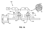
[0031] 図1A及び図1Bは、それぞれ本開示の態様が実装され得るリソグラフィ装置100及びリソグラフィ装置100’の概略図である。リソグラフィ装置100及びリソグラフィ装置100’はそれぞれ以下の、放射ビームB(例えば深紫外放射又は極端紫外放射)を調節するように構成された照明システム(イルミネータ)ILと、パターニングデバイス(例えばマスク、レチクル、又は動的パターニングデバイス)MAを支持するように構成されるとともに、パターニングデバイスMAを正確に位置決めするように構成された第1のポジショナPMに接続された支持構造(例えばマスクテーブル)MTと、基板(例えばレジストコートウェーハ)Wを保持するように構成されるとともに、基板Wを正確に位置決めするように構成された第2のポジショナPWに接続された基板テーブル(例えばウェーハテーブル)WTとを備える。リソグラフィ装置100及び100’は、パターニングデバイスMAにより放射ビームBに付与されたパターンを基板Wのターゲット部分(例えば1つ以上のダイを含む)Cに投影するように構成された投影システムPSも有する。リソグラフィ装置100では、パターニングデバイスMA及び投影システムPSは反射型である。リソグラフィ装置100’では、パターニングデバイスMA及び投影システムPSは透過型である。
[0030] Exemplary Lithography System
1A and 1B are schematic diagrams of
[0032] 照明システムILは、放射ビームBを誘導し、整形し、又は制御するための、屈折型、反射型、反射屈折型、磁気型、電磁型、静電型、又はその他のタイプの光学コンポーネント、あるいはそれらの任意の組み合わせ等の様々なタイプの光学コンポーネントを含むことができる。 [0032] The illumination system IL may include various types of optical components, such as refractive, reflective, catadioptric, magnetic, electromagnetic, electrostatic or other types of optical components, or any combination thereof, for directing, shaping or controlling the radiation beam B.
[0033] 支持構造MTは、基準フレームに対するパターニングデバイスMAの方向、リソグラフィ装置100及び100’のうちの少なくとも1つの設計、及びパターニングデバイスが真空環境で保持されているか否か等の他の条件に応じた手法で、パターニングデバイスMAを保持する。支持構造MTは、機械的、真空、静電、又は他のクランプ技術を使用して、パターニングデバイスMAを保持することができる。支持構造MTは、例えば、フレーム又はテーブルでもよく、必要に応じて固定式又は可動式でよい。センサを使用することにより、支持構造MTは、パターニングデバイスMAが例えば投影システムPSに対して確実に所望の位置に来るようにできる。
[0033] The support structure MT holds the patterning device MA in a manner that depends on the orientation of the patterning device MA relative to a reference frame, the design of at least one of
[0034] 「パターニングデバイス」MAという用語は、基板Wのターゲット部分Cにパターンを生成する等のために放射ビームBの断面にパターンを付与するのに使用され得る何らかのデバイスを指すものと広義に解釈されるべきである。放射ビームBに付与されたパターンは、集積回路を形成するためにターゲット部分Cに生成されるデバイスにおける特定の機能層に対応する可能性がある。 [0034] The term "patterning device" MA should be interpreted broadly to refer to any device that can be used to impart a pattern to a radiation beam B in its cross-section, such as to create a pattern in a target portion C of a substrate W. The pattern imparted to the radiation beam B may correspond to a particular functional layer in a device being created in the target portion C to form an integrated circuit.
[0035] 本明細書において、「検査装置」、「メトロロジシステム」等の用語は、例えば構造の特性(例えば、オーバーレイ誤差、クリティカルディメンションパラメータ)を測定するために使用されるデバイス又はシステム、あるいは、ウェーハのアライメント(例えばアライメント装置)を検査するためにリソグラフィ装置内で使用されるデバイス又はシステムを指すために使用される場合がある。 [0035] As used herein, the terms "inspection apparatus," "metrology system," etc. may be used to refer to a device or system used, for example, to measure characteristics of structures (e.g., overlay error, critical dimension parameters) or to a device or system used in a lithography apparatus to inspect the alignment of a wafer (e.g., an alignment apparatus).
[0036] パターニングデバイスMAは、(図1Bのリソグラフィ装置100’におけるように)透過型であっても、(図1Aのリソグラフィ装置100におけるように)反射型であってもよい。パターニングデバイスMAの例には、レチクル、マスク、プログラマブルミラーアレイ、又はプログラマブルLCDパネルが含まれる。マスクはリソグラフィにおいて周知であり、バイナリマスク、レベンソン型位相シフトマスク、又はハーフトーン型位相シフトマスク、並びに、多様なハイブリッドマスクタイプ等のマスクタイプを含む。プログラマブルミラーアレイの一例は、それぞれが入射する放射ビームを異なる方向に反射するように個別に傾斜され得る小さいミラーのマトリクス配列を採用する。傾斜されたミラーは、小さいミラーのマトリクスにより反射される放射ビームBにパターンを付与する。
[0036] Patterning device MA may be transmissive (as in lithographic apparatus 100' of FIG. 1B) or reflective (as in
[0037] 「投影システム」PSという用語は、用いられる露光放射線に、又は、基板W上の液浸液の使用もしくは真空の使用等の他の要素に適切な、屈折型、反射型、屈折反射型、磁気型、電磁型、静電型光学システム、又はそれらのいずれかの組み合わせを含む、任意のタイプの投影システムを含んでいてもよい。その他のガスは放射線又は電子を吸収し過ぎる可能性があるため、EUV又は電子ビーム放射線には真空環境を使用することがある。したがって、真空環境は、真空壁及び真空ポンプを用いてビーム経路全体に提供してもよい。 [0037] The term "projection system" PS may include any type of projection system including refractive, reflective, refractive-reflective, magnetic, electromagnetic, electrostatic optical systems, or any combination thereof, appropriate to the exposure radiation used or other factors such as the use of an immersion liquid on the substrate W or the use of a vacuum. A vacuum environment may be used for EUV or electron beam radiation, as other gases may be too absorbing of the radiation or electrons. A vacuum environment may therefore be provided throughout the beam path using a vacuum wall and vacuum pumps.
[0038] リソグラフィ装置100及び/又はリソグラフィ装置100’は、2つ(デュアルステージ)又はそれ以上の基板テーブルWT(及び/又は2つ以上のマスクテーブル)を有するタイプであってよい。このような「マルチステージ」機械においては、追加の基板テーブルWTが並行して使用されるか、あるいは1つ以上の基板テーブルWTが露光に使用されている間に、1つ以上の他のテーブルで準備工程が実行されてよい。ある状況では、追加のテーブルは基板テーブルWTでなくてもよい。
[0038]
[0039] リソグラフィ装置は、投影システムと基板との間の空間を充填するように、基板の少なくとも一部を水等の比較的高い屈折率を有する液体で覆うことができるタイプでもよい。液浸液は、例えばマスクと投影システムの間等、リソグラフィ装置の他の空間に適用することもできる。液浸技術は、投影システムの開口数を増加させるために当技術分野でよく知られている。本明細書で使用する「液浸」という用語は、基板等の構造を液体に沈めなければならないという意味ではなく、露光中に投影システムと基板の間に液体が存在するというほどの意味である。 [0039] The lithographic apparatus may be of a type in which at least a part of the substrate may be covered with a liquid having a relatively high refractive index, such as water, so as to fill a space between the projection system and the substrate. Immersion liquids may also be applied to other spaces in the lithographic apparatus, for example between the mask and the projection system. Immersion techniques are well known in the art for increasing the numerical aperture of projection systems. The term "immersion" as used herein does not mean that a structure such as the substrate must be submerged in liquid, but rather that liquid is present between the projection system and the substrate during exposure.
[0040] 図1A及び図1Bを参照すると、イルミネータILは放射源SOから放射ビームを受ける。例えば放射源SOがエキシマレーザである場合、例えば放射源SOとリソグラフィ装置100,100’とは別個の物理的実体であってよい。この場合、放射源SOはリソグラフィ装置100又は100’の一部を形成するとは見なされず、放射ビームBは放射源SOから、例えば適切な誘導ミラー及び/又はビームエキスパンダを備えたビームデリバリシステムBD(図1B)を介してイルミネータILへ進む。他の場合、例えば放射源SOが水銀ランプである場合には、放射源SOはリソグラフィ装置100,100’の一体部分であってよい。放射源SOとイルミネータILとは、またビームデリバリシステムBDが必要とされる場合にはこれも合わせて、放射システムと呼ばれることがある。
1A and 1B, the illuminator IL receives a radiation beam from a radiation source SO. For example, the source SO and the
[0041] イルミネータILは放射ビームの角強度分布を調整するためのアジャスタAD(図1B)を備えてよい。一般に、イルミネータの瞳面における強度分布の少なくとも外側及び/又は内側半径範囲(一般にそれぞれ「σ-outer」及び「σ-inner」と呼ばれる)を調整することができる。更に、イルミネータILはインテグレータIN及びコンデンサCO等の他の様々なコンポーネント(図1B)を備えてもよい。イルミネータILは、ビーム断面における所望の均一性及び強度分布を得るために放射ビームBを調節するのに使用することができる。 [0041] The illuminator IL may comprise an adjuster AD (Figure 1B) for adjusting the angular intensity distribution of the radiation beam. Generally, at least the outer and/or inner radial extent (commonly referred to as "σ-outer" and "σ-inner", respectively) of the intensity distribution in a pupil plane of the illuminator may be adjusted. Furthermore, the illuminator IL may comprise various other components, such as an integrator IN and a condenser CO (Figure 1B). The illuminator IL can be used to adjust the radiation beam B to obtain a desired uniformity and intensity distribution in its cross-section.
[0042] 図1Aを参照すると、放射ビームBは、支持構造(例えばマスクテーブル)MTに保持されたパターニングデバイス(例えばマスク)MAに入射し、パターニングデバイスMAによってパターン付与される。リソグラフィ装置100では、放射ビームBはパターニングデバイス(例えばマスク)MAから反射される。パターニングデバイス(例えばマスク)MAから反射された後、放射ビームBは投影システムPSを通過する。投影システムPSは放射ビームBを基板Wのターゲット部分Cに合焦させる。第2のポジショナPWと位置センサIF2(例えば、干渉デバイス、リニアエンコーダ、又は静電容量センサ)の助けによって、基板テーブルWTを(例えば、放射ビームBの経路に異なるターゲット部分Cを位置決めするように)正確に移動させることができる。同様に、第1のポジショナPM及び別の位置センサIF1を使用して、放射ビームBの経路に対してパターニングデバイス(例えばマスク)MAを正確に位置決めすることができる。マスクアライメントマークM1、M2及び基板アライメントマークP1、P2を使用して、パターニングデバイス(例えばマスク)MA及び基板Wを位置合わせすることができる。
[0042] Referring to FIG. 1A, a radiation beam B is incident on a patterning device (e.g. mask) MA, which is held on a support structure (e.g. mask table) MT, and is patterned by the patterning device MA. In the
[0043] 図1Bを参照すると、放射ビームBは、支持構造(例えばマスクテーブルMT)に保持されたパターニングデバイス(例えばマスクMA)に入射し、パターニングデバイスによってパターン付与される。マスクMAを横断した後、放射ビームBは投影システムPSを通過する。投影システムPSはビームを基板Wのターゲット部分Cに合焦させる。投影システムは、照明システム瞳IPUと共役な瞳PPUを有する。放射の一部は、照明システム瞳IPUにおける強度分布から生じ、マスクパターンにおいて回折の影響を受けることなくマスクパターンを横切り、照明システム瞳IPUにおいて強度分布の像を生成する。 [0043] Referring to FIG. 1B, the radiation beam B is incident on a patterning device (e.g. mask MA), which is held on a support structure (e.g. mask table MT), and is patterned by the patterning device. After traversing the mask MA, the radiation beam B passes through a projection system PS, which focuses the beam onto a target portion C of a substrate W. The projection system has a pupil PPU that is conjugate with the illumination system pupil IPU. A portion of the radiation originates from the intensity distribution in the illumination system pupil IPU and traverses the mask pattern without being subject to diffraction at the mask pattern to produce an image of the intensity distribution in the illumination system pupil IPU.
[0044] 投影システムPSは、マスクパターンMPの像を投影する。像は、強度分布からの放射によりマークパターンMPから生成された回折ビームによって、基板W上に被覆されたフォトレジスト層上に形成される。例えば、マスクパターンMPには、ラインとスペースのアレイが含まれてよい。アレイでの放射回折でゼロ次回折でないものからは、ラインと垂直な方向に方向が変わった誘導回折ビームが生成される。非回折ビーム(すなわち、いわゆるゼロ次回折ビーム)は、伝搬方向が変化することなくパターンを横断する。ゼロ次回折ビームは、投影システムPSの共役な瞳PPUの上流にある投影システムPSの上部レンズ又は上部レンズグループを横断して、共役な瞳PPUに到達する。共役な瞳PPUの面における強度分布の、ゼロ次回折ビームに関連する部分は、照明システムILの照明システム瞳IPUの強度分布の像である。開口デバイスPDは、例えば投影システムPSの共役な瞳PPUを含む平面に又は実質的にその平面に配置される。 [0044] The projection system PS projects an image of the mask pattern MP. The image is formed on a photoresist layer coated on the substrate W by diffracted beams generated from the mark pattern MP by radiation from the intensity distribution. For example, the mask pattern MP may include an array of lines and spaces. Non-zero order diffraction of radiation at the array generates stimulated diffracted beams redirected perpendicular to the lines. The non-diffracted beams (i.e. the so-called zero order diffracted beams) traverse the pattern without changing their propagation direction. The zero order diffracted beams traverse an upper lens or an upper lens group of the projection system PS upstream of the conjugate pupil PPU of the projection system PS and reach the conjugate pupil PPU. The part of the intensity distribution in the plane of the conjugate pupil PPU that is associated with the zero order diffracted beams is an image of the intensity distribution in the illumination system pupil IPU of the illumination system IL. The aperture device PD is for example arranged in or substantially in a plane that includes the conjugate pupil PPU of the projection system PS.
[0045] 投影システムPSは、レンズ又はレンズグループLによって、ゼロ次回折ビームのみならず1次又は1次以上の回折ビーム(図示せず)も捕捉するように配置される。いくつかの態様では、ラインに対して垂直な方向に延びるラインパターンを結像するためのダイポール照明を使用して、ダイポール照明の解像度向上効果を利用することができる。例えば、1次回折ビームは、対応するゼロ次回折ビームにウェーハWのレベルで干渉して、ラインパターンMPの像を可能な限り高い解像度及びプロセスウィンドウ(すなわち、使用可能焦点深度及び許容露光ドーズの変化の組み合わせ)で生成する。いくつかの態様では、照明システム瞳IPUの反対象限に放射極(図示せず)を提供することによって非点収差を低減することができる。更に、いくつかの態様では、反対象限の放射極に関連付けられた投影システムの共役な瞳PPUにおいてゼロ次ビームを遮断することによって非点収差を低減することができる。このことは2009年3月31日発行の米国特許第7,511,799号により詳細に説明されており、その全体が参照により本明細書に組み込まれる。 [0045] The projection system PS is arranged to capture not only the zeroth order diffracted beam but also the first or higher order diffracted beams (not shown) by means of a lens or lens group L. In some aspects, the resolution enhancement effect of dipole illumination can be exploited by using dipole illumination to image a line pattern extending in a direction perpendicular to the line. For example, a first order diffracted beam interferes with a corresponding zeroth order diffracted beam at the level of the wafer W to generate an image of the line pattern MP with the highest possible resolution and process window (i.e., a combination of usable depth of focus and allowable exposure dose variation). In some aspects, astigmatism can be reduced by providing a pole (not shown) at the anti-symmetry limit of the illumination system pupil IPU. Furthermore, in some aspects, astigmatism can be reduced by blocking the zeroth order beam at the conjugate pupil PPU of the projection system associated with the anti-symmetry limit pole. This is explained in more detail in U.S. Pat. No. 7,511,799, issued Mar. 31, 2009, which is incorporated herein by reference in its entirety.
[0046] 第2のポジショナPW及び位置センサIFD(例えば、干渉デバイス、リニアエンコーダ、又は静電容量センサ)の助けにより、(例えば放射ビームBの経路に異なるターゲット部分Cを位置決めするように)基板テーブルWTを正確に移動させることができる。同様に、第1のポジショナPM及び別の位置センサ(図1Bに図示せず)を使用して、(例えばマスクライブラリの機械的な取り出し後又はスキャン中に)放射ビームBの経路に対してマスクMAを正確に位置決めすることができる。 [0046] With the aid of a second positioner PW and a position sensor IFD (e.g. an interferometric device, a linear encoder or a capacitive sensor), the substrate table WT can be accurately moved (e.g. to position different target portions C in the path of the radiation beam B). Similarly, the first positioner PM and a further position sensor (not shown in FIG. 1B) can be used to accurately position the mask MA with respect to the path of the radiation beam B (e.g. after mechanical removal of the mask library or during a scan).
[0047] 一般に、マスクテーブルMTの移動は、第1のポジショナPMの一部を形成するロングストロークモジュール(粗動位置決め)及びショートストロークモジュール(微動位置決め)の助けを借りて実現することができる。同様に、基板テーブルWTの移動は、第2のポジショナPWの一部を形成するロングストロークモジュール及びショートストロークモジュールを使用して実現することができる。ステッパの場合(スキャナとは対照的に)、マスクテーブルMTをショートストロークアクチュエータのみに接続するか又は固定してもよい。マスクMA及び基板Wは、マスクアライメントマークM1、M2及び基板アライメントマークP1、P2を使用して位置合わせすることができる。(図示のような)基板アライメントマークは、専用のターゲット部分を占有するが、ターゲット部分の間の空間に位置してもよい(スクライブラインアライメントマークとして周知である)。同様に、マスクMA上に複数のダイが設けられている状況では、マスクアライメントマークはダイ間に配置してもよい。 [0047] In general, movement of the mask table MT may be realized with the aid of a long-stroke module (coarse positioning) and a short-stroke module (fine positioning), which form part of the first positioner PM. Similarly, movement of the substrate table WT may be realized using a long-stroke module and a short-stroke module, which form part of the second positioner PW. In the case of a stepper (as opposed to a scanner), the mask table MT may be connected to a short-stroke actuator only, or may be fixed. The mask MA and substrate W may be aligned using mask alignment marks M1, M2 and substrate alignment marks P1, P2. The substrate alignment marks (as shown) occupy dedicated target portions, but may also be located in spaces between the target portions (known as scribe-lane alignment marks). Similarly, in situations in which more than one die is provided on the mask MA, the mask alignment marks may be located between the dies.
[0048] マスクテーブルMT及びパターニングデバイスMAは、真空チャンバV内にあってよい。真空内ロボットIVRを用いて、マスク等のパターニングデバイスを真空チャンバ内及び外に移動させることができる。代替的に、マスクテーブルMT及びパターニングデバイスMAが真空チャンバの外側にある場合、真空内ロボットIVRと同様に、様々な輸送作業のために真空外ロボットを用いることができる。真空内及び真空外ロボットは、共に中継ステーションの固定されたキネマティックマウントへの任意のペイロード(例えばマスク)のスムーズな移動のために較正される必要がある。 [0048] The mask table MT and patterning device MA may be in a vacuum chamber V. An in-vacuum robot IVR may be used to move a patterning device such as a mask in and out of the vacuum chamber. Alternatively, if the mask table MT and patterning device MA are outside the vacuum chamber, an out-vacuum robot may be used for various transport operations, similar to the in-vacuum robot IVR. Both the in-vacuum and out-vacuum robots need to be calibrated for smooth movement of any payload (e.g. a mask) to the fixed kinematic mount of the transfer station.
[0049] リソグラフィ装置100及び100’は、以下のモードのうち少なくとも1つにて使用可能である。
[0049]
[0050] 1.ステップモードでは、支持構造(例えばマスクテーブル)MT及び基板テーブルWTは、基本的に静止状態に維持される一方、放射ビームBに付与されたパターン全体が1回でターゲット部分Cに投影される(すなわち単一静的露光)。次に、別のターゲット部分Cを露光できるように、基板テーブルWTがX方向及び/又はY方向にシフトされる。 [0050] 1. In step mode, the support structure (e.g. mask table) MT and substrate table WT are kept essentially stationary, while the entire pattern imparted to the radiation beam B is projected onto the target portion C in one go (i.e. a single static exposure). The substrate table WT is then shifted in the X and/or Y direction so that a different target portion C can be exposed.
[0051] 2.スキャンモードでは、支持構造(例えばマスクテーブル)MT及び基板テーブルWTは、同期的にスキャンされる一方、放射ビームBに付与されたパターンがターゲット部分Cに投影される(すなわち単一動的露光)。支持構造(例えばマスクテーブル)MTに対する基板テーブルWTの速度及び方向は、投影システムPSの拡大(縮小)及び像反転特性によって求めることができる。 [0051] 2. In scan mode, the support structure (e.g. mask table) MT and the substrate table WT are scanned synchronously while a pattern imparted to the radiation beam B is projected onto a target portion C (i.e. a single dynamic exposure). The velocity and direction of the substrate table WT relative to the support structure (e.g. mask table) MT can be determined by the (de-)magnification and image reversal characteristics of the projection system PS.
[0052] 3.別のモードでは、支持構造(例えばマスクテーブル)MTはプログラマブルパターニングデバイスを保持して基本的に静止状態に維持され、基板テーブルWTを移動又はスキャンさせながら、放射ビームBに付与されたパターンがターゲット部分Cに投影される。パルス放射源SOを使用することができ、プログラマブルパターニングデバイスは、基板テーブルWTを移動させる毎に、又はスキャン中に連続する放射パルスの間で、必要に応じて更新される。この動作モードは、プログラマブルミラーアレイ等のプログラマブルパターニングデバイスを利用するマスクレスリソグラフィに容易に適用できる。 [0052] 3. In another mode, the support structure (e.g. mask table) MT is kept essentially stationary holding a programmable patterning device and the substrate table WT is moved or scanned while a pattern imparted to the radiation beam B is projected onto a target portion C. A pulsed radiation source SO can be used and the programmable patterning device is updated as required after each movement of the substrate table WT, or between successive radiation pulses during a scan. This mode of operation is readily adaptable to maskless lithography employing a programmable patterning device such as a programmable mirror array.
[0053] 上述した使用モードの組み合わせ及び/又は変形、あるいは全く異なる使用モードも利用できる。 [0053] Combinations and/or variations on the above described modes of use or entirely different modes of use may also be employed.
[0054] 更なる態様では、リソグラフィ装置100は、極端紫外(EUV)放射源を備える。極端紫外放射源は、EUVリソグラフィのためにEUV放射ビームを発生させるように構成される。一般に、EUV放射源は放射システム内に構成され、対応する照明システムはEUV放射源のEUV放射ビームを調節するように構成される。
[0054] In a further aspect, the
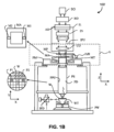
[0055] 図2は、ソースコレクタ装置SO、照明システムIL、及び投影システムPSを備えたリソグラフィ装置100をより詳細に示している。ソースコレクタ装置SOは、ソースコレクタ装置SOの閉鎖構造220内に真空環境を維持できるように構築及び配置される。放電生成プラズマ源によってEUV放射放出プラズマ210を形成することができる。EUV放射を生成するには、例えばXeガス、Li蒸気、又はSn蒸気のようなガス又は蒸気によって、極めて高温のプラズマ210を生成して、電磁スペクトルのEUV範囲内の放射を放出させればよい。極めて高温のプラズマ210は、例えば放電によって少なくとも不完全電離プラズマを生じさせることによって生成される。効率的な放射発生のため、例えば分圧が10PaのXe、Li、Snの蒸気又は他のいずれかの適切なガスもしくは蒸気が必要となることがある。いくつかの態様では、励起したスズ(Sn)のプラズマを供給してEUV放射を生成する。
[0055] Figure 2 shows the
[0056] 高温プラズマ210が放出した放射は、放射源チャンバ211からコレクタチャンバ212内へ、放射源チャンバ211の開口内又は開口の後ろに位置決めされた任意選択のガスバリア又は汚染物質トラップ230(場合によっては汚染物質バリア又はフォイルトラップとも呼ばれる)を介して送出される。汚染物質トラップ230はチャネル構造を含むことができる。汚染物質トラップ230は、ガスバリア又はガスバリアとチャネル構造の組み合わせを含むこともできる。本明細書で更に示す汚染物質トラップ又は汚染物質バリア230は、少なくともチャネル構造を含む。
[0056] Radiation emitted by the
[0057] コレクタチャンバ212は、いわゆるかすり入射型コレクタの場合もある放射コレクタCOを含むことができる。放射コレクタCOは、上流放射コレクタ側251及び下流放射コレクタ側252を有する。コレクタCOを横断する放射は、格子スペクトルフィルタ240で反射して、仮想光源点INTFに合焦させることができる。仮想光源点INTFは一般に中間焦点と呼ばれ、ソースコレクタ装置は、中間焦点INTFが閉鎖構造220の開口219に又はその近傍に位置するように配置される。仮想光源点INTFは、放射放出プラズマ210の像である。格子スペクトルフィルタ240は、特に赤外線(IR)放射を抑制するために用いられる。
[0057] The
[0058] この後、放射は照明システムILを横断する。照明システムILは、パターニングデバイスMAにおいて放射ビーム221の所望の角度分布を与えるとともにパターニングデバイスMAにおいて所望の放射強度均一性を与えるように配置されたファセットフィールドミラーデバイス222及びファセット瞳ミラーデバイス224を備えることができる。支持構造MTにより保持されたパターニングデバイスMAにおいて放射ビーム221が反射されると、パターン付きビーム226が形成され、パターン付きビーム226は、反射要素228,229を介して投影システムPSによって、ウェーハステージ又は基板テーブルWTにより保持された基板W上に結像される。
[0058] The radiation then traverses an illumination system IL, which may comprise a faceted
[0059] 一般に、照明光学ユニットIL及び投影システムPSには、図示するよりも多くの要素が存在することができる。格子スペクトルフィルタ240は、リソグラフィ装置のタイプに応じて任意選択的に存在することができる。更に、図2に示したものよりも多くのミラーが存在することができ、例えば投影システムPSには、図2に示したものよりも1つから6つの追加の反射要素が存在することができる。
[0059] In general, there may be more elements in the illumination optics unit IL and projection system PS than shown. A grating
[0060] 図2に示すようなコレクタ系COは、コレクタ(又はコレクタミラー)の単なる一例として、かすり入射型リフレクタ253、254、及び255を有する入れ子状のコレクタとして示されている。かすり入射型リフレクタ253、254、及び255は、光軸Oを中心として軸方向に対称配置され、このタイプのコレクタ系COは、好適にはDPP源と呼ばれることが多い放電生成プラズマ源と組み合わせて用いられる。
2 is shown as a nested collector with
[0061] 例示的リソグラフィセル
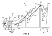
[0062] 図3は、いくつかの態様に従ったリソセル又はクラスタと呼ばれることもあるリソグラフィセル300を示している。リソグラフィ装置100又は100’はリソグラフィセル300の一部を形成することができる。リソグラフィセル300は、基板に露光前プロセス及び露光後プロセスを実行する1つ以上の装置を含むこともできる。従来から、これらにはレジスト層を堆積させるためのスピンコータSC、露光したレジストを現像するためのデベロッパDE、冷却プレートCH、及びベークプレートBKが含まれる。基板ハンドラ、すなわちロボットROが、入出力ポートI/O1,I/O2から基板を取り出し、それらを様々なプロセス装置間で移動させ、リソグラフィ装置100又は100’のローディングベイLBに引き渡す。これらのデバイスは、まとめてトラックと呼ばれることも多く、トラック制御ユニットTCUの制御下にある。TCU自体は監視制御システムSCSによって制御され、監視制御システムSCSはリソグラフィ制御ユニットLACUを介してリソグラフィ装置も制御する。したがって、これらの様々な装置はスループット及び処理効率を最大化するように動作させることができる。
[0061] Exemplary Lithography Cell
[0062] Figure 3 illustrates a
[0063] 例示的検査装置
[0064] デバイスフィーチャを基板上に正確に配置するためのリソグラフィプロセスを制御するために、一般にアライメントマークが基板上に提供され、リソグラフィ装置は、基板上のマークの正確な位置決めのための1つ以上の検査装置を含む。これらのアライメント装置は、効果的な位置測定装置である。様々なタイプのマーク及び様々なタイプのアライメント装置及び/又はシステムは、様々な時点及び様々な製造業者から知られている。現行のリソグラフィ装置において幅広く使用されるシステムのタイプは、米国特許第6,961,116号(den Boef等)に記載されるような自己参照干渉計に基づく。一般に、マークは、X位置及びY位置を取得するために別々に測定される。しかしながら、組み合わされたX測定及びY測定は、米国特許公開第2009/195768号(BiJnen等)に記載される技法を使用して実行可能である。これら開示の両方の全内容は、参照により本明細書に組み込まれる。
[0063] Exemplary Inspection Apparatus
[0064] To control the lithography process for accurate placement of device features on the substrate, alignment marks are typically provided on the substrate and the lithography apparatus includes one or more inspection apparatus for accurate positioning of the marks on the substrate. These alignment apparatus are effectively position measurement apparatus. Various types of marks and various types of alignment apparatus and/or systems are known from different times and different manufacturers. A type of system that is widely used in current lithography apparatus is based on a self-referencing interferometer as described in U.S. Pat. No. 6,961,116 (den Boef et al.). Typically, the marks are measured separately to obtain the X and Y positions. However, combined X and Y measurements can be performed using the technique described in U.S. Patent Publication No. 2009/195768 (BiJnen et al.). The entire contents of both of these disclosures are incorporated herein by reference.
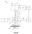
[0065] 図4Aは、いくつかの態様に従ったリソグラフィ装置100又は100’の一部として実装可能な検査装置400の断面ビューを示す概略図である。いくつかの態様において、検査装置400は、パターニングデバイス(例えばパターニングデバイスMA)に対して基板(例えば基板W)を位置合わせするように構成可能である。検査装置400は、基板上のアライメントマークの位置を検出するように、及び、アライメントマークの検出された位置を使用してリソグラフィ装置100又は100’のパターニングデバイス又は他の構成要素に対して基板を位置合わせするように更に構成可能である。こうした基板のアライメントは、基板上の1つ以上のパターンの正確な露光を保証することができる。
[0065] FIG. 4A is a schematic diagram illustrating a cross-sectional view of an
[0066] いくつかの態様において、検査装置400は、照明システム412、ビームスプリッタ414、干渉計426、ディテクタ428、ビーム分析器430、及びオーバーレイ計算プロセッサ432を含むことができる。照明システム412は、1つ以上の通過帯域を有する電磁狭帯域放射ビーム413を提供するように構成可能である。一例において、1つ以上の通過帯域は、約500nmから約900nmの間の波長のスペクトル内とすることができる。別の例において、1つ以上の通過帯域は、約500nmから約900nmの間の波長のスペクトル内の離散的狭通過帯域とすることができる。照明システム412は、長い時間期間にわたって(例えば照明システム412の寿命にわたって)、実質的に一定の中心波長(CWL)値を有する1つ以上の通過帯域を提供するように更に構成可能である。こうした照明システム412の構成は、現行のアライメントシステムにおいて、上記で考察したように、所望のCWL値からの実際のCWL値のシフトを防ぐために役立つことができる。また結果として、一定のCWL値の使用は、現行のアライメント装置と比較して、アライメントシステム(例えば検査装置400)の長期安定性及び確度を向上させることができる。
[0066] In some aspects, the
[0067] いくつかの態様において、ビームスプリッタ414は、放射ビーム413を受け取り、放射ビーム413を少なくとも2つの放射サブビームに分割するように構成可能である。例えば、放射ビーム413は、図4Aに示されるように放射サブビーム415及び417に分割可能である。ビームスプリッタ414は、放射サブビーム415をステージ422上に配置された基板420上に誘導するように更に構成可能である。一例において、ステージ422は方向424に沿って移動可能である。放射サブビーム415は、基板420上に配置されたアライメントマーク又はターゲット418を照明するように構成可能である。アライメントマーク又はターゲット418は、放射感応性フィルムでコーティング可能である。いくつかの態様において、アライメントマーク又はターゲット418は、180度(すなわち180°)対称性を有することができる。すなわち、アライメントマーク又はターゲット418がアライメントマーク又はターゲット418の平面に対して垂直な対称性の軸の周りを180°回転すると、回転したアライメントマーク又はターゲット418は、回転していないアライメントマーク又はターゲット418と実質的に同一であり得る。基板420上のターゲット418は、(a)実レジストラインから形成されるバーを含むレジスト層格子、又は(b)プロダクトレイヤ格子、又は(c)プロダクトレイヤ格子上にオーバーレイ又はインターリーブされたレジスト格子を備える、オーバーレイターゲット構造における複合格子スタックとすることができる。バーは、代替として基板内にエッチング可能である。このパターンは、リソグラフィ投影装置、特に、投影システムPLにおいて、色収差に対して敏感であり、照明対称性及びこうした収差の存在は、プリント格子における変動においてそれら自体を表すことになる。ライン幅、ピッチ、及びクリティカルディメンションの測定のためのデバイス製造で使用される1つのインライン方法は、「スキャトロメトリ」と呼ばれる技法を利用する。スキャトロメトリの方法は、Raymond等の「Multiparameter Grating Metrology Using Optical Scatterometry」,J.Vac.Sci.Tech.B,Vol.15,no.2,pp。361-368(1997)及び、Niu等の「Specular Spectroscopic Scatterometry in DUV Lithography」,SPIE,Vol.3677(1999)に記載されており、その両方の全体が参照により本明細書に組み込まれる。スキャトロメトリにおいて、光はターゲット内の周期構造によって反射され、所与の角度で結果として生じる反射スペクトルが検出される。反射スペクトルを引き起こす構造は、例えば、Rigorous Coupled-Wave Analysis(RCWA)を使用して、又は、シミュレーションによって導出されるパターンのライブラリと比較することによって、再構築される。したがって、プリント格子のスキャトロメトリデータは、格子を再構築するために使用される。ライン幅及び形状等の格子のパラメータは、プリンティングステップ及び/又は他のスキャトロメトリプロセスの知識から、処理ユニットPUによって実行される再構築プロセスに入力可能である。
[0067] In some embodiments, the
[0068] いくつかの態様において、ビームスプリッタ414は、一態様に従って、回折放射ビーム419を受け取り、回折放射ビーム419を少なくとも2つの放射サブビームに分割するように更に構成可能である。回折放射ビーム419は、図4Aに示されるように回折放射サブビーム429及び439に分割可能である。
[0068] In some embodiments, the
[0069] たとえビームスプリッタ414が、放射サブビーム415をアライメントマーク又はターゲット418に向けて誘導し、回折放射サブビーム429を干渉計426に向けて誘導するように示されている場合であっても、本開示はそのように限定されないことに留意されたい。当業者であれば、他の光学配置を使用して、基板420上のアライメントマーク又はターゲット418を照明し、アライメントマーク又はターゲット418の像を検出することと同様の結果を得ることが可能であることが明らかとなろう。
[0069] Note that even though
[0070] 干渉計426は、図4Aに示されるように、ビームスプリッタ414を介して放射サブビーム417及び回折放射サブビーム429を受け取るように構成可能である。例示の態様において、回折放射サブビーム429は、アライメントマーク又はターゲット418から反射可能な放射サブビーム415の少なくとも一部とすることができる。本態様の一例において、干渉計426は、任意の適切な光学要素のセット、例えば、受け取った回折放射サブビーム429に基づいてアライメントマーク又はターゲット418の2つの像を形成するように構成可能なプリズムの組み合わせを備える。良好な品質の像が形成される必要はないが、アライメントマーク418のフィーチャは解決されるべきであることを理解されたい。干渉計426は、2つの像のうちの一方を2つの像のうちの他方に対して180°回転させ、回転された像及び回転されない像を干渉法的に再組み合わせするように更に構成可能である。
[0070] Interferometer 426 can be configured to receive
[0071] いくつかの態様において、ディテクタ428は、干渉計信号427を介して再組み合わせされた像を受け取り、検査装置400のアライメント軸421がアライメントマーク又はターゲット418の対称の中心(図示せず)を通過する際に再組み合わせされた像の結果として干渉を検出するように構成可能である。こうした干渉は、例示の態様に従い、アライメントマーク又はターゲット418が180°対称であること、及び、再組み合わせされた画像が建設的又は破壊的に干渉することに起因する可能性がある。検出された干渉に基づいて、ディテクタ428は、アライメントマーク又はターゲット418の対称性の中心の位置を決定し、結果として基板420の位置を検出するように更に構成可能である。一例によれば、アライメント軸421は、基板420に垂直であり像回転干渉計426の中心を通過する光学ビームと位置合わせ可能である。ディテクタ428は、センサ特徴を実装すること及びウェーハマークプロセス変動と相互作用することによって、アライメントマーク又はターゲット418の位置を推定するように更に構成可能である。
[0071] In some embodiments, the
[0072] 更なる態様において、ディテクタ428は、下記の測定のうちの1つ以上を実行することによって、アライメントマーク又はターゲット418の対称性の中心の位置を決定する。
1.様々な波長についての位置変動(色間の位置シフト)を測定すること、
2.様々な次数についての位置変動(回折次数間の位置シフト)を測定すること、及び、
3.様々な極性についての位置変動(極性間の位置シフト)を測定すること。
[0072] In a further aspect, the
1. Measuring the position variation for different wavelengths (position shift between colors);
2. Measuring the position variation for the various orders (position shift between the diffraction orders), and
3. Measuring the position variation for different polarities (position shift between polarities).
[0073] 本データは、任意のタイプのアライメントセンサ、例えば、単一のディテクタ及び4つの異なる波長を備える自己参照干渉計を採用し、ソフトウェア内のアライメント信号を抽出する、米国特許第6,961,116号に記載されるようなSMASH(SMart Alignment Sensor Hybrid)センサ、又は、7つの回折次数の各々を専用ディテクタに誘導する、米国特許第6,297,876号に記載されるようなAthena(Advanced Technology using High order ENhancement of Alignment)を用いて取得可能であり、その両方の全体が参照により本明細書に組み込まれる。 [0073] This data can be obtained using any type of alignment sensor, such as the SMASH (SMart Alignment Sensor Hybrid) sensor as described in U.S. Pat. No. 6,961,116, which employs a self-referencing interferometer with a single detector and four different wavelengths and extracts the alignment signal in software, or the Athena (Advanced Technology using High order Enhancement of Alignment) sensor as described in U.S. Pat. No. 6,297,876, which directs each of the seven diffraction orders to a dedicated detector, both of which are incorporated herein by reference in their entirety.
[0074] いくつかの態様において、ビーム分析器430は、回折放射サブビーム439の光学状態を受け取り、決定するように構成可能である。光学状態は、ビーム波長、極性、又はビームプロファイルの測定とすることができる。ビーム分析器430は、ステージ422の位置を決定し、ステージ422の位置をアライメントマーク又はターゲット418の対称性の中心の位置と相関させるように更に構成可能である。したがって、アライメントマーク又はターゲット418の位置及び結果として基板420の位置を、ステージ422に対して正確に知ることができる。代替として、ビーム分析器430は、検査装置400又は任意の他の基準要素を参照してアライメントマーク又はターゲット418の対称性の中心を知ることができるよう、検査装置400又は任意の他の基準要素の位置を決定するように構成可能である。ビーム分析器430は、波長帯域選択性の何らかの形を伴うポイント又は結像偏光計とすることができる。いくつかの態様において、ビーム分析器430は、検査装置400内に直接統合するか、又は、他の態様に従って、偏光保持単一モード、マルチモード、又は結像等のいくつかのタイプの光ファイバを介して接続可能である。
[0074] In some aspects, the
[0075] いくつかの態様において、ビーム分析器430は、基板420上の2つのパターン間のオーバーレイデータを決定するように更に構成可能である。これらのパターンのうちの1つは基準層上の基準パターンとすることができる。他のパターンは露光層上の露光パターンとすることができる。基準層は、基板420上に既に存在するエッチング層とすることができる。基準層は、リソグラフィ装置100及び/又は100’によって基板上に露光される基準パターンによって発生可能である。露光層は、基準層に近接して露光されるレジスト層とすることができる。露光層は、リソグラフィ装置100又は100’により基板420上で露光される露光パターンによって発生可能である。基板420上の露光パターンは、ステージ422による基板420の動きに対応することができる。いくつかの態様において、測定されたオーバーレイデータは、基準パターンと露光パターンとの間のオフセットを示すことも可能である。測定されたオーバーレイデータは、リソグラフィ装置100又は100’によって露光される露光パターンを較正するために、較正データとして使用可能であり、較正後、露光層と基準層との間のオフセットを最小限にすることができる。
[0075] In some aspects, the
[0076] いくつかの態様において、ビーム分析器430は、基板420のプロダクトスタックプロファイルのモデルを決定するように更に構成可能であり、単一測定において、オーバーレイ、クリティカルディメンション、及びターゲット418の焦点を測定するように構成可能である。プロダクトスタックプロファイルは、アライメントマーク、ターゲット418、又は基板420等のスタックされたプロダクトに関する情報を含み、照明変動の関数であるマークプロセス変動誘導型光学署名メトロロジを含むことができる。プロダクトスタックプロファイルは、プロダクト格子プロファイル、マークスタックプロファイル、及びマーク非対称性上方も含むことができる。ビーム分析器430の一例は、米国特許第8,706,442号に記載されるようなオランダ国フェルドホーフェンのASMLによって製造されるYieldstar(商標)であり、その全体が参照により本明細書に組み込まれる。ビーム分析器430は、その層内の露光パターンの特定の特性に関する情報を処理するように更に構成可能である。例えば、ビーム分析器430は、オーバーレイパラメータ(基板上の前の層に関する層の位置決め確度又は基板上のマークに関する第1の層の位置決め確度のインジケーション)、焦点パラメータ、及び/又は、層内に示された像のクリティカルディメンションパラメータ(例えばライン幅及びその変動)を処理することができる。他のパラメータは、露光パターンの示された像の品質に関する像パラメータである。
[0076] In some embodiments, the
[0077] いくつかの態様において、ディテクタのアレイ(図示せず)がビーム分析器430に接続可能であり、下記で考察するように、正確なスタックプロファイル検出の可能性を許可する。例えばディテクタ428は、ディテクタのアレイであり得る。ディテクタアレイの場合、マルチモードファイバのバンドル、チャネルごとの離散ピンディテクタ、あるいは、CCD又はCMOS(リニア)アレイという、いくつかのオプションが可能である。マルチモードファイバのバンドルの使用は、安定性のために、任意の消散要素をリモートに配置することができる。離散PINディテクタは、大きなダイナミックレンジを提供するが、それぞれに別々のプリアンプが必要である。そのため、要素の数は制限される。CCDリニアアレイは、位相ステッピング検出が使用される場合、高速で読み出し可能であり、特に注目される多くの要素を提供する。
[0077] In some embodiments, an array of detectors (not shown) can be connected to the
[0078] いくつかの態様において、第2のビーム分析器430’は、図4Bに示されるように回折放射サブビーム429の光学状態を受け取り決定するように構成可能である。光学状態は、ビーム波長、極性、又はビームプロファイルの測定であり得る。第2のビーム分析器430’は、ビーム分析器430と同一であり得る。代替として、第2のビーム分析器430’は、ステージ422の位置を決定すること、及び、ステージ422の位置をアライメントマーク又はターゲット418の対称性の中心の位置と相関させること等の、ビーム分析器430の少なくともすべての機能を実行するように構成可能である。したがって、アライメントマーク又はターゲット418の位置及び結果として基板420の位置を、ステージ422を参照しながら正確に知ることができる。第2のビーム分析器430’は、検査装置400又は任意の他の基準要素を参照してアライメントマーク又はターゲット418の対称性の中心を知ることができるよう、検査装置400又は任意の他の基準要素の位置を決定するようにも構成可能である。第2のビーム分析器430’は、2つのパターン間のオーバーレイデータ、及び、基板420のプロダクトスタックプロファイルのモデルを決定するように更に構成可能である。第2のビーム分析器430’は、単一の測定において、ターゲット418のオーバーレイ、クリティカルディメンション、及び焦点を測定するようにも構成可能である。
[0078] In some embodiments, the second beam analyzer 430' can be configured to receive and determine the optical state of the diffracted
[0079] いくつかの態様において、第2のビーム分析器430’は、検査装置400内に直接統合するか、又は、他の態様に従って、偏光保持単一モード、マルチモード、又は結像等のいくつかのタイプの光ファイバを介して接続可能である。代替として、第2のビーム分析器430’及びビーム分析器430は、回折放射サブビーム429及び439の両方の光学状態を受け取り決定するように構成された単一の分析器(図示せず)を形成するために組み合わせ可能である。
[0079] In some embodiments, the second beam analyzer 430' can be integrated directly into the
[0080] いくつかの態様において、プロセッサ432は、ディテクタ428及びビーム分析器430から情報を受信する。例えば、プロセッサ432はオーバーレイ計算プロセッサとすることができる。情報は、ビーム分析器430によって構築されるプロダクトスタックプロファイルのモデルを含むことができる。代替として、プロセッサ432は、プロダクトマークに関する受信した情報を使用してプロダクトマークプロファイルのモデルを構築することができる。いずれの場合にも、プロセッサ432は、プロダクトマークプロファイルのモデルを使用するか又は組み込む、スタックされたプロダクト及びオーバーレイマークプロファイルのモデルを構築する。次いで、スタックモデルを使用して、オーバーレイオフセットが決定され、オーバーレイオフセット測定に対するスペクトル効果を最小限にする。プロセッサ432は、照明ビームの光学状態、アライメント信号、関連付けられた位置推定値、並びに瞳、像、及び追加の平面内の光学状態を含むが限定されない、ディテクタ428及びビーム分析器430から受信した情報に基づいて、基本補正アルゴリズムを作成することができる。瞳面は、放射の放射位置が入射の角度を画定し、角度位置が放射のアジマス角を画定する平面である。プロセッサ432は、ウェーハマーク及び/又はアライメントマーク418に関して検査装置400を特徴付けるために、基本の補正アルゴリズムを利用することができる。
[0080] In some aspects, the
[0081] いくつかの態様において、プロセッサ432は、ディテクタ428及びビーム分析器430から受信した情報に基づいて、各マークについてのセンサ推定に対するプリントパターン位置オフセット誤差を決定するように更に構成可能である。情報は、プロダクトスタックプロファイル、オーバーレイの測定、クリティカルディメンション、及び基板420上の各アライメントマーク又はターゲット418の焦点を含むが限定されない。プロセッサ432は、クラスタ化アルゴリズムを利用して、マークを同様の一定のオフセット誤差のセットにグループ化し、情報に基づいてアライメント誤差オフセット補正表を作成することができる。クラスタ化アルゴリズムは、オフセット誤差の各セットに関連付けられた、オーバーレイ測定、位置推定、及び追加の光学スタックプロセス情報に基づくことが可能である。オーバーレイは、例えば、プログラムされたオーバーレイオフセット周りに正及び負のバイアスを有するオーバーレイターゲット等の、異なるマークの数について計算される。最小のオーバーレイを測定するターゲットが基準として(最良の確度で測定されるものとして)採用される。この測定された最小のオーバーレイ、及び、それに対応するターゲットの既知のプログラムされたオーバーレイから、オーバーレイ誤差を推測することができる。表1は、これがどのように実行できるかを示す。示された例の最小の測定されたオーバーレイは-1nmである。しかしながら、これは-30nmのプログラムされたオーバーレイを伴うターゲットに関する。プロセスは29nmのオーバーレイ誤差をもたらし得る。
[0081] In some aspects, the
[0082] 最小値は基準点として採用可能であり、これに関して、測定されたオーバーレイとプログラムされたオーバーレイに起因して予測されたオーバーレイとの間のオフセットが計算可能である。このオフセットは、各マーク又は同様のオフセットを伴うマークのセットについてのオーバーレイ誤差を決定する。したがって、表1の例において、30nmのプログラムされたオーバーレイを伴うターゲット位置での、最小の測定されたオーバーレイは-1nmであった。他のターゲットでの予測されたオーバーレイと測定されたオーバーレイとの差は、この基準と比較される。表1のような表は、異なる照明設定の下でマーク及びターゲット418から取得することも可能であり、結果として最小オーバーレイ誤差を生じさせる照明設定、及び、それに対応する較正係数を決定及び選択可能である。これに続いて、プロセッサ432は、マークを同様のオーバーレイのセットにグループ化することができる。マークをグループ化するための基準は、様々なプロセス制御、例えば様々なプロセスについての様々な誤差許容値に基づいて、調整可能である。
[0082] The minimum value can be taken as a reference point, for which an offset between the measured overlay and the predicted overlay due to the programmed overlay can be calculated. This offset determines the overlay error for each mark or a set of marks with a similar offset. Thus, in the example of Table 1, at the target location with a programmed overlay of 30 nm, the minimum measured overlay was -1 nm. The difference between the predicted and measured overlay at other targets is compared to this reference. A table such as Table 1 can also be obtained from the marks and
[0083] いくつかの態様において、プロセッサ432は、グループのすべて又はほとんどのメンバーが、同様のオフセット誤差を有していることを認識し、追加の光学スタックメトロロジに基づいて、クラスタ化アルゴリズムから各マークに個々のオフセット補正を適用することが可能である。プロセッサ432は、各マークについての補正を決定し、オーバーレイにおける誤差を補正するために、例えば、補正を検査装置400内へとフィードすることによって、補正をリソグラフィ装置100又は100’へとフィードバックすることができる。
[0083] In some aspects,
[0084] 例示的作動ステージ
[0085] いくつかの態様において、「スループット」という用語は、ウェーハが特定の製作ステップをクリアし、次のステップへと移動する速度を記述するために使用可能である。スループットは、リソグラフィシステムの市場性の性能マーカとすることができる。リソグラフィシステムでは、可能な限り短時間で可能な限り多くの製品を出力することが望ましい。リソグラフィ製作は、いくつかの複雑な製作プロセスを含むことができる。各製作プロセスは、望ましい製作品質と欠点とのバランス(例えば、サブナノメータ精度、ウェーハ当たりの高収率、高スループット等に対する、低速製作、印刷エラー、コスト等)を保つ技術的特徴を有する。
[0084] Exemplary Operational Stages
[0085] In some embodiments, the term "throughput" can be used to describe the speed at which a wafer clears a particular fabrication step and moves to the next step. Throughput can be a performance marker for marketability of a lithography system. In a lithography system, it is desirable to output as much product as possible in as little time as possible. Lithography fabrication can include several complex fabrication processes. Each fabrication process has technical characteristics that balance the desired fabrication quality with drawbacks (e.g., sub-nanometer accuracy, high yield per wafer, high throughput, etc. versus slow fabrication, printing errors, cost, etc.).
[0086] リソグラフィ装置(又は検査装置)において、ウェーハ又はレチクルは、所与の速さで所与の方向にスキャン可能である。ウェーハ及びレチクルは、高速移動ステージ上にあるチャック上で支持可能である。しかしながら、高加速度からの力が、チャックを歪曲(例えば伸長)させる可能性があり、これがウェーハ又はレチクルの位置決めエラーを発生させる可能性がある。位置決めエラーは、ウェーハから製造されるデバイスの印刷エラーを生じさせる可能性がある。 [0086] In a lithography apparatus (or inspection apparatus), a wafer or reticle can be scanned in a given direction at a given speed. The wafer and reticle can be supported on a chuck that is on a fast moving stage. However, forces from high accelerations can distort (e.g. stretch) the chuck, which can cause positioning errors of the wafer or reticle. The positioning errors can cause printing errors of devices manufactured from the wafer.
[0087] 本明細書で開示される態様は、空間要件、複雑さ、及びコストに関してごくわずかな譲歩を伴って可動ステージの構造上の問題に対処するための、デバイス及び機能を含む。 [0087] The embodiments disclosed herein include devices and features to address the structural challenges of moving stages with minimal compromise in terms of space requirements, complexity, and cost.
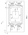
[0088] 図5は、いくつかの態様に従ったオブジェクト502を支持するためのステージ500を示す。いくつかの態様において、ステージ500は、支持構造504(例えば第1の支持構造)、支持構造506(例えば第2の支持構造)、アクチュエータデバイス510、及びアクチュエータターゲット508を備えることができる。アクチュエータデバイス510は、コイル巻線512を備えることができる。アクチュエータターゲット508は、固定構造514(例えばエポキシ)を使用して支持構造504上に配設及び固定可能である。アクチュエータ関係要素の数及び構成は、図5に示されるものに限定されない。より少ないか又はより多いアクチュエータ関係要素、及び他の構成が使用可能である。ステージ500は、1つ以上の位置インジケータ516(例えばエンコーダスケール)も備えることができる。
[0088] FIG. 5 illustrates a
[0089] いくつかの態様において、数え上げ形容詞(例えば、「第1」、「第2」、「第3」、等)は命名規則として使用可能であり、(特に記載のない限り)順序又は階層を示すことは意図されていないことを理解されたい。例えば、「第1の支持構造」及び「第2の支持構造」という用語は、2つの支持構造を区別することは可能であるが、支持構造が特定の順序又は階層を有するかどうかを指定する必要はない。更に、図面内の要素は、いずれの特定の数え上げ形容詞にも限定されない。例えば、1つのアクチュエータデバイス510は、他方のアクチュエータデバイスが数え上げ形容詞を適切に区別することを使用する場合、第2のアクチュエータデバイスと呼ぶことができる。別の非限定的な例では、上部右のアクチュエータデバイス510を第1のアクチュエータデバイスとして命名することを選択し、その後、残りのアクチュエータデバイスを、時計回り、反時計回り、十字パターン等の順に第2、第3、及び第4として識別することができる。
[0089] It should be understood that in some embodiments, enumeration adjectives (e.g., "first," "second," "third," etc.) can be used as a naming convention and are not intended to indicate order or hierarchy (unless otherwise noted). For example, the terms "first support structure" and "second support structure" may distinguish between two support structures, but need not specify whether the support structures have a particular order or hierarchy. Furthermore, the elements in the figures are not limited to any particular enumeration adjectives. For example, one
[0090] いくつかの態様において、ステージ500は、リソグラフィ装置100又は100’(図1A、図1B、及び図2)、リソグラフィセル300(図3)、検査装置400(図4A及び図4B)、又は、一般にオブジェクトを支持及び移動するためのステージ実装を有する任意の装置において、使用可能である。例えば、ステージ500は、ウェーハテーブルWT又はマスクテーブルMT(図1A、図1B、及び図2)、あるいはステージ422(図4A及び図4B)の、特定の実装を示すことができる。
[0090] In some aspects,
[0091] いくつかの態様において、支持構造506は、(例えばオブジェクト502の粗動のための)作動構造とすることができる。リソグラフィ製造プロセスにおいて、オブジェクト502は、例えば直径300mm(これは、当業者であれば理解されるように、ウェーハが異なるサイズで市販されている非限定的例である)の半導体ウェーハとすることができる。更に、ステージ500は、オブジェクト502をローディングエリアとの間で往復させるための追加の移動バジェットも含むことができる。したがって、支持構造506は、ステージ500の、例えば数十、数百、又は数千ミリメートルほどの粗動を担うことができる。特定の実装に対する適合性に基づいて、他の距離も選択可能である。しかしながら、粗動が必要でない実装では、支持構造506は静的フレームとすることができる。
[0091] In some embodiments, the
[0092] いくつかの態様において、支持構造504は、2つの支持構造間の相対的な移動も可能にしながら、支持構造506によって支持可能である。支持構造504の運動は、ガイドレール又は非接触法(例えば磁気浮揚)を使用する軸(例えばY軸)に限定することができる(ガイドデバイスは図示せず)。アクチュエータデバイス510は、支持構造504の位置の微調整を担うことができる。したがって、いくつかの態様は、アクチュエータデバイス510とそれらの対応するアクチュエータターゲット508との間の小さなギャップを使用する。例えばギャップは、数ミリメートル以下(例えばおよそ1mm未満)とすることができる。スキャニングリソグラフィプロセスにおいて、プリントデバイスは、サブミクロン又はサブナノメートル範囲内の限界寸法を有することができる。1ミリメートルの移動バジェットが、サブナノメートルデバイスのスキャンプリンティングには十分な大きさとすることができる。
[0092] In some embodiments, the
[0093] いくつかの態様において、アクチュエータデバイス510を支持構造506上に配設及び固定することができる。アクチュエータデバイス510は、アクチュエータターゲット508と相互作用することによって、支持構造504を作動させることができる。アクチュエータターゲット508は、磁界に反応する材料(例えば、金属、鉄、フェライト等)を備えることができる。アクチュエータデバイス510は、電磁石とすることができる。電磁石は、磁界を生成及び調整することができる。電磁石は、金属コア(例えばフェライトコア)の周囲に巻きつけられたワイヤのコイル512を備えることができる。アクチュエータデバイス510は、アクチュエータターゲット508が永久磁石でない場合に引き付けるのみとして動作可能である。逆に、アクチュエータデバイス510は、磁界の方向を反転させることによって、アクチュエータターゲット508の永久磁石バージョンに反発すること及び引き付けることが可能である。本明細書で説明するアクチュエータセットアップは、他の技術的用語で呼ぶことができる。(例えばリラクタンスアクチュエータ。したがってアクチュエータターゲット508はリラクタンスターゲットと呼ぶことができる。)
[0093] In some embodiments, the
[0094] いくつかの態様において、アクチュエータデバイス510は、高加速度を使用して支持構造504を作動させることができる。加速度は、例えば、およそ4~100g、10~50g、20~40g等(ここで、gは9.8m/s2である)とすることができる。高加速度は、リソグラフィ印刷生産を向上させる(例えば、スループットを向上させる)ことができる。リソグラフィパターン転写は、支持構造504が運動中であるとき、例えば一定の惰行速さに達したときに実行可能である。惰行速さは、例えば、0.5~10.0m/s、1.0~7.0m/s、3.0~5.0m/s等とすることができる。一定のスキャニング速さでパターン転写を実行することで、結果として、印刷パターンのより正確な転写が生じる可能性がある一方で、加速中の印刷は、より大きな位置の不確実性を伴う可能性がある。
[0094] In some embodiments, the
[0095] いくつかの態様において、磁界の性質は反発相互作用が不安定であり、望ましくない横力(反発の方向に対して直交)及び望ましくない直交トルクを生成する可能性がある。直交力/トルクは、磁石セットの合計ポテンシャルエネルギーを最小にするために、反発から誘引へと相互作用を変化させるように磁石を移動させる傾向がある。外部側方誘導又は抑圧力無しでは、配置は不安定であり、ギャップを閉じながら(もはや浮遊しておらず)最も近い安定した均衡位置へとジャンプする。したがって、永久磁石を使用する反発システムは、エンジニアには困難である可能性があり、配置を崩壊させないようにアクティブ制御の追加又は外部機械的ガイドを促すことができる。リソグラフィシステムの複雑さが追加されると、エンジニアリングの困難さを著しく増加させる可能性がある。したがって、いくつかの態様において、アクチュエータデバイス510は、誘引のみ(又はプルのみ)を使用して動作するように設計可能である。支持構造504の反対側にアクチュエータデバイス510があると、プルのみの構成を使用しながら、支持構造504に対して前方及び後方の両方の運動を伝えることが可能である。しかしながら、プルのみの方法は、下記でより詳細に考察するように特定の欠点を有する可能性がある。
[0095] In some embodiments, the nature of the magnetic field is such that the repulsive interaction is unstable and can generate undesirable lateral forces (orthogonal to the direction of repulsion) and undesirable orthogonal torques. The orthogonal forces/torques tend to move the magnets to change the interaction from repulsion to attraction in order to minimize the total potential energy of the magnet set. Without an external lateral guidance or restraining force, the configuration is unstable and jumps to the nearest stable equilibrium position while closing the gap (no longer floating). Thus, a repulsive system using permanent magnets can be challenging for engineers and may prompt the addition of active controls or external mechanical guides to keep the configuration from collapsing. The added complexity of the lithography system can significantly increase the engineering difficulty. Thus, in some embodiments, the
[0096] いくつかの態様において、オブジェクト502を支持構造504上に押し付けることによって、オブジェクト502を一時的に支持構造504上に固定することができる。これは、真空クランプ(吸引力)、静電クランプ(静電力)、機械的クランプ等によって、達成可能である。理想的な条件の下では、オブジェクト502(例えばレチクル)と支持構造504(例えばチャック)との間の相互摩擦が、それらの間に滑りがないことを保証可能である。しかしながら、高加速度に起因する機械的応力は、何らかの滑りを誘導し、結果として印刷エラーを生じさせる可能性がある。エラーは、エラーが検出可能な時間による何千というデバイス製品の損失の可能性に起因して、かなり有害である可能性がある。
[0096] In some embodiments, the
[0097] 下記は、ステージ500を使用する際のオブジェクト502の位置決めエラーの一例である。いくつかの態様において、オブジェクト502は支持構造504上に固定可能である。オブジェクト502上のフィーチャの位置を決定するために、例えば、光学検査システムを使用して、較正測定を実行することができる。較正測定は、1つ以上の位置インジケータ516に対するオブジェクト502上のフィーチャの位置を決定することができる。位置インジケータ516は、支持構造504に堅固に固定可能である。オブジェクト502と1つ以上の位置インジケータ516との間の関係が確立されると、オブジェクト502は、高精度プロセス(例えばリソグラフィプロセス)に使用可能であり、オブジェクト502が支持構造504に対して依然として定常である限り、較正を実施する必要はない。逆に、オブジェクト502と支持構造504との間の任意の相対的運動は、位置決めエラー、すなわち、エラー事象の発生後、続いて、あらゆるプロセスに伝達されるエラーと見なされる可能性がある。
[0097] The following is an example of a positioning error of the
[0098] 下記は、位置決めエラーを誘導する可能性のある条件及び機構の一例である。いくつかの態様において、アクチュエータデバイス510によってアクチュエータターゲット508に電磁力を印加することができる。例えば、支持構造504の左側のアクチュエータデバイス510を活動化し、その後、対応するアクチュエータ508、固定構造514、及び最終的に支持構造504をプルすることができる。その結果、支持構造504の右側のアクチュエータデバイス510は、反対方向に(減速のために)プルするため、及び支持構造504を静止させることを可能にするために、使用可能となる。加速/減速の間、オブジェクト502及び支持構造504の組み合わせられた質量は慣性であり、プル(右を指す矢印「ma」(質量×加速)として描かれる)の間、アクチュエータターゲット508によって及ぼされる力に等しい、反対の力を及ぼす。逆に、2つのアクチュエータターゲット508がプルを実行している場合、プルの力は、2つのアクチュエータターゲット508に分割する(2本の矢印「F=ma/2」として描かれる)ことができる。
[0098] The following are examples of conditions and mechanisms that may induce positioning errors. In some embodiments, an electromagnetic force may be applied to the
[0099] プルのみ方式の欠点は、いくつかの態様において、支持構造504が、高加速度(例えば4~100g)に起因する高張力勾配の下にあり得ることである。張力は、支持構造504を変形(例えば伸長)させる可能性がある。たとえ支持構造504が堅固な構造で作られている(例えば、ガラス及びリブ強化材で作られている)場合であっても、たとえ数ピコメートルの変形でも、1つ以上の位置インジケータ516に対してオブジェクト502を数ピコメートルシフトさせる可能性があり、それによって位置決めエラーをもたらす。プル-プッシュ方式(いくつかのアクチュエータデバイス510がプルし、いくつかが後ろからプッシュする)は、引張及び変形の問題の多くに対抗するが、磁気の反発に関する前述の問題をもたらすことにもなる。
[0099] A drawback of the pull-only approach is that in some embodiments, the
[0100] プルのみ方式の別の欠点は、いくつかの態様において、固定構造514も、高加速度に起因する著しい張力の下にあり得ることである。固定構造514がエポキシで作られる非限定的例において、張力のみの下にあるエポキシは、クリープする(例えば、経時的にゆっくりと広がる)可能性があり、エポキシ応力の平均がゼロであるプル-プッシュ方式と比較すると、機械的障害の可能性を増加させる(例えば、一方向のプルの場合は張力下であるが、反対方向のプッシュの場合は圧縮下でもある)。
[0100] Another drawback of the pull-only approach is that in some embodiments, the anchoring
[0101] 本明細書で説明するいくつかの態様は、プルのみ方式の問題に対処するための構造及び機能を提供する。 [0101] Some aspects described herein provide structures and functionality to address the issues of pull-only approaches.
[0102] 図6は、いくつかの態様に従ったオブジェクト602を支持するためのステージ600を示す。いくつかの態様において、ステージ600は、図5を参照しながら既に説明したいくつかのフィーチャを有することができる。図6と比較すると、いくつかの要素は(明瞭にするために)非表示であり得るが追加の要素が示され得る。別段に記載されていない限り、図5の要素について事前に説明した構造及び機能は、図6の同様に番号付けされた(例えば、参照番号は右端の2つの数字を共有している)要素にも適用可能である。図6の要素の少なくともいくつかの構造及び機能は、図5の対応する要素の説明から明らかとなるものであり、再度紹介はしない。
[0102] FIG. 6 illustrates a
[0103] いくつかの態様において、ステージ500(図5)のフィーチャに加え、ステージ600は、追加の内部アクチュエータデバイス610i及び伸張構造618(例えばカンチレバー)も備えることができる。アクチュエータデバイス610と同様に、内部アクチュエータデバイス610iは支持構造606上に配設及び固定することができる。伸張構造618を使用して、アクチュエータターゲット608を支持構造604の側部から離れて固定構造614(例えばエポキシ)を活用して構造的に固定することができる。伸張構造618によって空間が作成されると、アクチュエータデバイス610iのうちの所与の1つを、(図6に示すように)その対応するアクチュエータターゲット608、その対応する伸張構造618、及び支持構造604の側部によって画定される内部空間内に配設することができる。
[0103] In some embodiments, in addition to the features of stage 500 (FIG. 5),
[0104] いくつかの態様において、ステージ600の構成を使用して、ステージ500について前述の問題のうちの少なくともいくつかを克服することができる(図6)。例えば、左側の2つのアクチュエータデバイス610は支持構造604をプルするためのものであるが、支持構造604の右側の別の2つの内部アクチュエータデバイス610iは、支持構造604を「プッシュ」するために使用可能である。4つの活動化されたアクチュエータデバイスは、「F=ma/4」とラベル表示された4本の矢印で示され、合計の力はそれらの対応する4つのアクチュエータターゲット608の間で分割される(より少ないか又はより多いアクチュエータデバイスが実装可能である)。しかしながら、右の2つのアクチュエータデバイス610iは、支持構造604を左側に移動させるために誘引(プル)を使用し、したがって、図6の方式はプル-プル方式と呼ぶことができる。結果として、前述の反発の問題を回避することが可能であり、同時に支持構造604の変形も減少させ、固定構造614にかかる応力の平衡も保つ(すなわち、張力の平衡化からの応力及び前後への移動からの圧縮の平均をゼロ化する)。運動の方向を減速及び/又は反転させるために、対応するアクチュエータデバイス610及び内部アクチュエータデバイス610iをプル-プル構成で使用可能である。
[0104] In some embodiments, the configuration of
[0105] いくつかの態様において、内部アクチュエータデバイス610i及び伸張構造618を追加することは、いくつかの望ましくない結果を有する可能性がある。1つの欠点は、構築のコストが増加する(追加部品及び製造の複雑さ)ことである。別の欠点は、構成要素を移動させる際、それらの慣性に加えて全重量が増加することである。図6において、粗動構造(支持構造606及びそれを支持するすべて)の質量は、4つの追加の重い電磁石(内部アクチュエータデバイス610i)に起因して増加する。微動構造(支持構造606及びそれを支持するすべて)の質量は、伸張構造618の追加に起因して増加する。更に、伸張構造618は振動に敏感な可能性があり、結果として支持構造604の運動においてダイナミクスが乏しいことになる。振動に起因する追加の不確実性は、オブジェクト602がリソグラフィプロセスのためのレチクルとして使用されるとき、パターン転写精度に影響を及ぼす。
[0105] In some embodiments, adding the
[0106] 本明細書に記載されるいくつかの態様は、プルのみ方式及びプル-プル方式の両方の問題に対処するための構造及び機能を提供する。 [0106] Some aspects described herein provide structures and functionality to address the issues of both pull-only and pull-pull approaches.
[0107] 図7A及び図7Bは、いくつかの態様に従ったオブジェクト702を支持するためのステージ700を示す。いくつかの態様において、ステージ700は、図5及び図6を参照しながら既に説明したいくつかのフィーチャを有することができる。図5及び図6と比較すると、いくつかの要素は(明瞭にするために)非表示であり得るが追加の要素が示され得る。別段に記載されていない限り、図5及び図6の要素について事前に説明した構造及び機能は、図7A及び図7Bの同様に番号付けされた(例えば、参照番号は右端の2つの数字を共有している)要素にも適用可能である。図7A及び図7Bの要素の少なくともいくつかの構造及び機能は、図5及び図6の対応する要素の説明から明らかとなるものであり、再度紹介はしない。
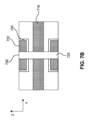
7A and 7B show a
[0108] 図7Aを参照すると、いくつかの態様において、ステージ500又は600(図5及び図6)のフィーチャに加えて(又は特定のフィーチャの代わりに)、ステージ700は、シャフト718を備えることができる。シャフト718は、留め具720(例えば、ピン、ボルト等)を使用して支持構造704に固定可能である。1つ以上の負荷スプレッダ722を使用して、留め具720の一部を取り囲むことができる。アクチュエータターゲット708の1つ以上をシャフト718(例えば、シャフトの各端部に1つのアクチュエータターゲット708)に固定することができる(固定は、溶接、接着剤、エポキシ等を介して達成可能である)。アクチュエータターゲット708は、1つ以上のスタビライザ724に結合可能である。シャフト実装は、図7Aに示されるように、複数のシャフト及び対応する取り付け要素を有するために、反復可能である。
[0108] Referring to FIG. 7A, in some embodiments, in addition to (or instead of) certain features of
[0109] いくつかの態様において、シャフト718は、支持構造704のロケーション726において支持構造704に固定することができる。ロケーション726は、支持構造704の中心線728(例えば、支持構造を2等分する中心線)にほぼ沿うことができる。対応するアクチュエータデバイス710がアクチュエータターゲット708をプルするために活動化されるとき、シャフト718は、アクチュエータターゲット708から支持構造704のロケーション726へと機械的負荷を伝達することができる。このように機械的負荷を分散させることによって、ステージ500(図5)の高張力勾配が減少する可能性がある。代わりに、歪み効果を、ロケーション726の左側への圧縮領域(プルの力が左に向かうことを想定)及びロケーション726の右側への引張領域に分割することができる。支持構造704の圧縮及び引張応力の再構成に起因して、オブジェクト702が滑りを経験するリスクを著しく減少させることができる。更に、同じシャフト718の反対端に固定された2つのアクチュエータターゲット708を有することで、機械的負荷をより均一に分散させることができる。例えば、1つのアクチュエータターゲットが左側にプルされる際、シャフトによって伝達される機械的負荷の一部は後続のアクチュエータターゲットに伝達される。後続アクチュエータによって及ぼされる力は支持構造704をプッシュ可能であり、それによって、チャックを伸長させる慣性傾向に対抗し、多くのスキャニングサイクルのエポキシ内の平均応力をゼロ化する。
[0109] In some embodiments, the
[0110] 図7Bは、いくつかの態様に従った支持構造704のロケーション726の断面を示す。いくつかの態様において、シャフト718は支持構造704の内部を通過することができる。しかしながら、シャフト718を支持構造704の外側(例えば、図7Aのページの配向を参照すると、支持構造704の上端、支持構造704の下端、支持構造704の表面上の凹部等)に取り付ける等の、他の実装が予想される。支持構造704は、ロケーション726においてホールを備えることができる。シャフト718は、支持構造704のホールと整合するホールも備えることができる。留め具720は、シャフトをロケーション726に固定するために、支持構造704及びシャフト718の両方のホール内に配設可能である。
[0110] FIG. 7B shows a cross section of a
[0111] いくつかの態様において、支持構造704は、ロケーション726におけるホールと整合する1つ以上のカウンターボアを備えることができる。負荷スプレッダ722は、加速中に機械的負荷を分散させるために各カウンターボア及び周囲の留め具720内に配設可能である。負荷スプレッダ722は、例えばダイアフラムフレクシャを備えることができる。1つ以上の負荷スプレッダ722は、接着構造730(エポキシ)を使用して皿穴に固定することができる。支持構造704の運動(例えば、前後左右にスキャンされる)を考慮すると、エポキシにかかる応力は圧縮及び張力の均衡を有し、これがステージ500(図5)内で使用されるエポキシ上の張力不均衡の問題に対処する。いくつかの態様において、設計は、留め具720と支持構造704との間に直接の接触が発生しないように、クリアランスホールが留め具720(図示せず)を取り囲むようなものであり得る。
[0111] In some embodiments, the
[0112] 図7Aに戻って参照すると、いくつかの態様において、ステージ700のフィーチャは、上記の欠点を緩和しながら、ステージ500及び600の特定の望ましいフィーチャを達成することができる。例えば、ステージ700のセットアップは、ステージ600(図6)と比較したとき、部品及びフットプリントを削減することができる。したがって、追加の内部アクチュエータデバイス610i及び伸張構造618(図6)を使用する必要がなくなり、コスト、重量、及び空間が削減される。ステージ500は、ステージ600(図6)より少ないアクチュエータデバイス510(図5)を使用し、高い張力及び変形の問題を有したが、ステージ700は、アクチュエータデバイスの数を増加させる必要がなく、張力変形を緩和することができる。
[0112] Referring back to FIG. 7A, in some embodiments, features of
[0113] いくつかの態様において、ステージ700は、ステージ700のダイナミクスを更に強化するための低容量ソリューションを実装することができる。例えば、スタビライザ724を使用して、振動の影響を低減させることができる。スタビライザ724は、アクチュエータターゲット708に結合可能である。スタビライザ724は、フレクシャを備えることができる。
[0113] In some embodiments, the
[0114] 図8は、いくつかの態様に従った支持構造804のセクションを示す。いくつかの態様において、支持構造804は、支持構造704(図7)と比較した際に、代替シャフト実装を有することができる。支持構造704の特定のフィーチャは、図を明瞭にするために示されていないことを理解されたい。しかしながら、支持構造804の更なるフィーチャは図5から図7の説明から明らかになるはずであり、再度紹介はしない。
[0114] FIG. 8 illustrates a section of a
[0115] いくつかの態様において、シャフト818は、アクチュエータターゲット(例えば708(図7))から支持構造804の複数のロケーションへと負荷を転移させるために使用可能である。支持構造804は、支持構造804の対応する第1、第2、及び/又は第3のロケーションにおいて、第1、第2、及び/又は第3のホールを備えることができる。シャフト818は、支持構造804の対応するホールと整合する、第1、第2、及び/又は第3のホールも備えることができる。留め具820は、支持構造804の第1、第2、及び/又は第3のロケーションにおいてシャフトを固定するために、支持構造804及びシャフト818の両方のホール内に配設することができる。すべての負荷を単一の留め具720(図7)上に置くことに対して、負荷を複数の留め具にわたって分散させることにより、留め具820の直径を留め具720(図7)よりも小さくすることが可能である。
[0115] In some embodiments, the
[0116] 引張部材を伴う例示的作動ステージ
[0117] 図9は、いくつかの態様に従ったオブジェクト(例えば、ウェーハ、レチクル等)を支持するためのステージ900の一部を示す。いくつかの態様において、ステージ900は、図5から図8を参照しながら既に説明したいくつかのフィーチャを有することができる。図5から図8と比較すると、いくつかの要素は(明瞭にするために)非表示であり得るが追加の要素が示され得る。別段に記載されていない限り、図5から図8の要素について事前に説明した構造及び機能は、図9の同様に番号付けされた(例えば、参照番号は右端の2つの数字を共有している)要素にも適用可能である。図9の要素の少なくともいくつかの構造及び機能は、図5から図8の対応する要素の説明から明らかとなろう。
[0116] Exemplary Actuation Stages with Tension Members
[0117] Figure 9 illustrates a portion of a
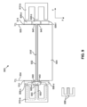
[0118] いくつかの態様において、ステージ900は、支持構造904、アクチュエータターゲット908(例えば3つ以上)、1つ以上のアクチュエータデバイス910、及び、引張部材918’を備えることができる。支持構造は、別の支持構造(例えば、図7A及び図7Bの支持構造706)上に乗っているチャックとすることができる。非限定的な例によれば、アクチュエータデバイス910-a及び910-bは、電磁石のE型コアとして示される。他のタイプの電磁石コアも予想される。例えば、図10のC型コアを参照するいくつかの態様が本明細書に開示される。図9には、ワイヤコイルは明示的に示されていないが、それらの存在及び機能は、当業者であれば以前の図面の説明(例えばコイル巻線512(図5))並びに磁界930に基づいて明らかとなろう。引張部材918’は、緩い又は柔軟な材料(例えばコード)、堅固なロッド等(例えばシャフト718(図7A及び図7B))とすることができる。
[0118] In some embodiments, the
[0119] いくつかの態様において、支持構造904は、空洞部分932(例えば、溝又はチャネル)を備えることができる。引張部材918’は、空洞部分932内に配設される。空洞部分932の寸法(例えば、断面、直径等)は、引張部材918’が空洞部分932内部に移動できるように、引張部材918’の寸法より大きいことが可能である。空洞部分932は、いくつかの異なる様式で(例えば、空洞チャネル、支持構造904外部の溝、1つ以上のリング等として)、実装可能である。アクチュエータターゲット908-a、908-b、908-c、908-d、908-e、908-fが、明示的に示されている(例えば、第1のアクチュエータターゲット、第2のアクチュエータターゲット、別のアクチュエータターゲット等)。しかし、より多いか又はより少ないアクチュエータターゲットが実装可能であることを理解されたい。
[0119] In some embodiments, the
[0120] いくつかの態様において、アクチュエータデバイス910-a及びアクチュエータターゲット908-a、908-c、及び908-eを、支持構造904の側部934(例えば第1の側部)に配設することができる。アクチュエータデバイス910-aは、(例えば、電磁石がオンになったとき、電磁石はアクチュエータターゲットを誘引できるように)、アクチュエータターゲット908-a、908-c、及び908-eの近位に配設することができる。アクチュエータデバイス910-b及びアクチュエータターゲット908-b、908-d、及び908-fは、支持構造904の側部934とは反対の側部936(例えば第2の側部)に配設することができる。アクチュエータデバイス910-bは、アクチュエータターゲット908-b、908-d、及び908-fの近位に配設することができる。
[0120] In some embodiments, actuator device 910-a and actuator targets 908-a, 908-c, and 908-e can be disposed on a side 934 (e.g., a first side) of
[0121] いくつかの態様において、E型コアの場合、E型コアの第1、第2、及び第3の構造上の突出部は、それぞれのアクチュエータターゲットに対向して配設することができる。C型コアは、同様に配置可能である(3つの突出部の代わりに、2つの突出部が2つのアクチュエータターゲットと対向している)。E型コアは、磁気透過性材料の単一ブロック又は2つ以上の部分のアセンブリ(例えば、互いに取り付けられた2つのC型コア938)から構築可能である。
[0121] In some embodiments, for an E-core, the first, second, and third structural protrusions of the E-core can be disposed facing the respective actuator targets. A C-core can be similarly arranged (with two protrusions facing two actuator targets instead of three). An E-core can be constructed from a single block of magnetically permeable material or an assembly of two or more pieces (e.g., two C-
[0122] いくつかの態様において、アクチュエータターゲット908-c及び908-eは、支持構造904の側部934に取り付けることができる。取り付けは、例えば、接着構造914(例えば、エポキシ等の接着剤)を使用して達成可能である。アクチュエータターゲット908-a及び908-bは、引張部材918’の反対端に取り付け可能である。例えば、支持構造904の側部934で磁界930を生成するために、アクチュエータデバイス910-aがオンになったとき、磁気相互作用は、所与の方向に沿って支持構造904を移動させるために、アクチュエータターゲット908-a、908-c、及び908-eを誘引することができる。更に、引張部材918’は、アクチュエータターゲット908-bを介して、機械的負荷を支持構造904の側部936に伝達することができる(例えば、機械的負荷転移は、第1のアクチュエータターゲット上に与えられる磁力に基づく)。
[0122] In some aspects, actuator targets 908-c and 908-e can be attached to a
[0123] いくつかの態様において、ターゲット908-a及び908-bの寸法(例えば、断面、直径)は、ターゲット908-a及び908-bが空洞部分932に入ることができないように、空洞部分932の寸法より大きいことが可能である。このシナリオでは、磁界930を使用してターゲット908-aをプルすることによって、ターゲット908-bは側部936上に「フック」することが可能であり、それによって、ターゲット908-c及び908-eを介して側部934で発生するプル運動を補完するために、支持構造904のプッシュ運動が可能になる。このようにして、支持構造904の加速度及び速さを増加させることが可能であり、更に、以前の図を参照しながら上記で説明したように、支持構造の一方の側部から単にプルすることの望ましくない影響を削減する(例えば変形)。
[0123] In some embodiments, the dimensions (e.g., cross-section, diameter) of targets 908-a and 908-b can be larger than the dimensions of
[0124] いくつかの態様において、アクチュエータターゲット908-bは、側部936へ伝達される機械的負荷を広げるために、負荷スプレッダ940を備えることができる。アクチュエータターゲット908-aは、負荷スプレッダ940も備えることができる。負荷スプレッダ940は、例えば、ソフトパッド、コイルばね、フレクシャ、折り畳み式構造等を、備えることができる。
[0124] In some embodiments, actuator target 908-b can include a
[0125] いくつかの態様において、アクチュエータターゲット908-aと908-cとの間の分離ギャップは、磁界930の減衰を防ぐために小さいものとすることができる。特に、近接するアクチュエータターゲット間のギャップは、アクチュエータターゲット(例えば908-a)とアクチュエータデバイス(例えば910-a)のポールとの間の動作ギャップよりもかなり小さいものとすることができる。非限定的な例では、かなり小さいとは、20%以下、15%以下、10%以下、5%以下、20%から5%、15%から5%、15%から10%、10%から5%等とすることができる。こうした条件が課されたとき、アクチュエータターゲット間のギャップによって生じるフラックス減少は、アクチュエータデバイスとアクチュエータターゲットとの間の動作ギャップによって生じるフラックス減少に比べて、無視できるほどのものとすることができる(例えば、無視できるほどとは、コイルを介する単位電流当たりの生成される力に対する数パーセント未満の影響とすることができる)。
[0125] In some embodiments, the separation gap between actuator targets 908-a and 908-c can be small to prevent attenuation of the
[0126] いくつかの態様において、アクチュエータデバイスとアクチュエータターゲットとの間の動作ギャップは、1500ミクロン以下、1000ミクロン以下、500ミクロン以下等とすることができる。500ミクロンの動作ギャップ及び10%以下の制約を非限定的な例として使用すると、2つのアクチュエータターゲット間の50ミクロンギャップは無視できるほどと見なすことができる。他方で、こうした小さなギャップを実用的又は経済的に製造することを妨げる、製造可能性上の問題が存在する場合がある。しかし、実用性の考慮は別として、ギャップが小さいほどアクチュエーション(例えば、コイル内の電流によって分割される力)の性能は良好である。 [0126] In some embodiments, the operating gap between the actuator device and the actuator target can be 1500 microns or less, 1000 microns or less, 500 microns or less, etc. Using a 500 micron operating gap and a 10% or less constraint as a non-limiting example, a 50 micron gap between two actuator targets can be considered negligible. On the other hand, there may be manufacturability issues that prevent such small gaps from being practical or economical to manufacture. However, practical considerations aside, the smaller the gap, the better the performance of the actuation (e.g., force divided by current in a coil).
[0127] いくつかの態様において、高い性能よりも製造コストの削減が好ましい場合、そのより緩い(おそらく、作るのがより容易な)許容範囲については、200ミクロン以下のギャップが望ましい可能性がある。トレードオフとして、より多くの電流を使用し、同じ出力でも加熱を悪化させる可能性もある。熱膨張の考慮も存在する。その電磁性能を最大にすることによって、アクチュエータデバイスによる熱生成を最小限にすることが望ましい。近接するアクチュエータターゲット908-aと908-cとの間の分離ギャップは、例えば、およそ2mm以下、1mm以下、500ミクロン以下、200ミクロン以下、100ミクロン以下、50ミクロン以下、20ミクロン以下、又は10ミクロン以下とすることができる。分離に関するこの特徴は、アクチュエータターゲット908-aと908-e、908-bと908-d、及び908-bと908-fの間の、ギャップにまで広げることができる。 [0127] In some embodiments, where reduced manufacturing costs are preferred over high performance, a gap of 200 microns or less may be desirable for its looser (and perhaps easier to make) tolerances. The tradeoff is to use more current and potentially worse heating for the same power output. There are also thermal expansion considerations. It is desirable to minimize heat generation by the actuator device by maximizing its electromagnetic performance. The separation gap between adjacent actuator targets 908-a and 908-c may be, for example, approximately 2 mm or less, 1 mm or less, 500 microns or less, 200 microns or less, 100 microns or less, 50 microns or less, 20 microns or less, or 10 microns or less. This separation feature may be extended to the gaps between actuator targets 908-a and 908-e, 908-b and 908-d, and 908-b and 908-f.
[0128] いくつかの態様において、支持構造904を図の左側に向けて(例えば、第1の方向に)移動させるための前述の機能は、反対方向の移動のために、アクチュエータデバイス910-b、並びに、アクチュエータターゲット908-b、908-d、及び908-fに対して、逆に適用できることを理解されよう。
[0128] It will be appreciated that in some embodiments, the functionality described above for moving
[0129] 図10は、いくつかの態様に従ったオブジェクト(例えば、ウェーハ、レチクル等)を支持するためのステージ1000の一部を示す。いくつかの態様において、ステージ1000は、図5から図9を参照しながら既に説明したいくつかのフィーチャを有することができる。図5から図9と比較すると、いくつかの要素は(明瞭にするために)非表示であり得るが追加の要素が示され得る。別段に記載されていない限り、図5から図9の要素について事前に説明した構造及び機能は、図10の同様に番号付けされた(例えば、参照番号は右端の2つの数字を共有している)要素にも適用可能である。図10の要素の少なくともいくつかの構造及び機能は、図5から図9の対応する要素の説明から明らかとなろう。
[0129] FIG. 10 illustrates a portion of a
[0130] いくつかの態様において、アクチュエータデバイス1010-aはC型コアとすることができる。アクチュエータターゲット1008-a及び1008-cは、アクチュエータデバイス1010-aのポールの近位に配設することができる。図10に示される他の要素の構造及び/又は機能は、以前の図を参照しながら上記で説明したものと同じとすることができる(例えば、支持構造1004、接着構造1014、引張部材1018’、磁界1030、空洞部分1032、側部1034、及び/又は負荷スプレッダ1040)。
[0130] In some embodiments, the actuator device 1010-a can be a C-core. The actuator targets 1008-a and 1008-c can be disposed proximate the pole of the actuator device 1010-a. The structure and/or function of the other elements shown in FIG. 10 can be the same as described above with reference to previous figures (e.g., the
[0131] 本文ではICの製造におけるリソグラフィ装置の使用に特に言及しているが、本明細書で説明するリソグラフィ装置には他の用途もあることを理解されたい。例えば、これは、集積光学システム、磁気ドメインメモリ用ガイダンス及び検出パターン、フラットパネルディスプレイ、LCD、薄膜磁気ヘッド等の製造である。こうした代替的な用途に照らして、本明細書で「ウェーハ」又は「ダイ」という用語を使用している場合、それぞれ「基板」又は「ターゲット部分」という、より一般的な用語の具体的な例と見なしてよいことが当業者には認識される。本明細書に述べている基板は、露光前又は露光後に、例えばトラックユニット(通常はレジストの層を基板に塗布し、露光したレジストを現像するツール)、及び/又はメトロロジユニットで処理することができる。適宜、本明細書の開示は、以上及びその他の基板プロセスツールに適用することができる。更に基板は、例えば多層ICを生成するために、複数回処理することができ、したがって本明細書で使用する基板という用語は、既に複数の処理済み層を含む基板も指すことができる。 [0131] Although specific reference is made herein to the use of lithographic apparatus in the manufacture of ICs, it should be understood that the lithographic apparatus described herein has other applications, such as the manufacture of integrated optical systems, guidance and detection patterns for magnetic domain memories, flat panel displays, LCDs, thin film magnetic heads, and the like. In light of these alternative applications, those skilled in the art will recognize that the use of the terms "wafer" or "die" herein may be considered specific examples of the more general terms "substrate" or "target portion", respectively. The substrates described herein may be processed, before or after exposure, for example in a track unit (a tool that typically applies a layer of resist to the substrate and develops the exposed resist), and/or in a metrology unit. Where appropriate, the disclosure herein may be applied to these and other substrate processing tools. Furthermore, the substrate may be processed multiple times, for example to produce a multi-layer IC, and thus the term substrate as used herein may also refer to a substrate that already includes multiple processed layers.
[0132] 光リソグラフィの分野での本開示の態様の使用に特に言及してきたが、本開示は文脈によってはその他の用途、例えばインプリントリソグラフィでも使用することができ、光リソグラフィに限定されないことを理解されたい。インプリントリソグラフィでは、パターニングデバイス内のトポグラフィが基板上に作成されたパターンを画定する。パターニングデバイスのトポグラフィは基板に供給されたレジスト層内に刻印され、電磁放射、熱、圧力又はそれらの組み合わせを適用することでレジストは硬化する。パターニングデバイスはレジストから取り除かれ、レジストが硬化すると、内部にパターンが残される。 [0132] Although specific reference has been made to the use of aspects of the present disclosure in the field of optical lithography, it should be understood that the present disclosure may also be used in other applications, such as imprint lithography, depending on the context, and is not limited to optical lithography. In imprint lithography, a topography in a patterning device defines the pattern created on a substrate. The topography of the patterning device is imprinted into a layer of resist supplied to the substrate, and the resist is cured by application of electromagnetic radiation, heat, pressure or a combination thereof. The patterning device is then removed from the resist leaving a pattern therein when the resist has hardened.
[0133] 本開示の言い回し又は専門用語は説明を目的とするものであって限定を目的とするものではないことが理解されるべきであり、従って、本開示の専門用語又は言い回しは、本開示の教示に照らして当業者によって解釈されるべきである。 [0133] It is to be understood that the phrases or terms of the present disclosure are for purposes of description and not of limitation, and as such, the phrases or terms of the present disclosure should be interpreted by one of skill in the art in light of the teachings of the present disclosure.
[0134] 本明細書で使用される「放射」、「放射のビーム」等の用語は、すべてのタイプの電磁放射、例えば、紫外線(UV)放射(例えば、365、248、193、157、又は126nmの波長λを有する)、極端紫外線(EUV又は軟X線)放射(例えば、5~20nm、例えば13.5nmの領域内の波長を有する)、又は、5nm未満で働く硬X線、あるいは、イオンビーム又は電子ビーム等の物質ビームを、包含可能である。「光」、「照明」等の用語は、非物質放射(例えば、光子、UV、X線等)を指すことができる。概して、約400から約700nmの間の波長を有する放射は、可視放射と見なされ、約780~3000nm(又はそれ以上)の間の波長を有する放射は、IR放射と見なされる。UVは、およそ100~400nmの波長を伴う放射を指す。リソグラフィ内では、「UV」という用語は、水銀放電ランプによって生成可能な波長、G線436nm、H線405nm、及び/又は、I線365nmにも適用される。真空UV、又はVUV(すなわち、ガスによって吸収されるUV)は、およそ100~200nmの波長を有する放射を指す。深UV(DUV)は、一般に、126nmから428nmの範囲の波長を有する放射を指し、いくつかの態様では、エキシマレーザがリソグラフィ装置内で使用されるDUV放射を生成することができる。例えば、5~20nmの範囲内の波長を有する放射は、特定の波長帯域を伴い、その少なくとも一部は5~20nmの範囲内である放射に関することを理解されたい。 [0134] As used herein, the terms "radiation", "beam of radiation", etc. can encompass all types of electromagnetic radiation, such as ultraviolet (UV) radiation (e.g., having a wavelength λ of 365, 248, 193, 157, or 126 nm), extreme ultraviolet (EUV or soft x-ray) radiation (e.g., having a wavelength in the range of 5-20 nm, e.g., 13.5 nm), or hard x-ray operating below 5 nm, or a matter beam such as an ion beam or an electron beam. Terms such as "light", "illumination", etc. can refer to non-material radiation (e.g., photons, UV, x-ray, etc.). Generally, radiation having a wavelength between about 400 and about 700 nm is considered visible radiation, and radiation having a wavelength between about 780-3000 nm (or greater) is considered IR radiation. UV refers to radiation with a wavelength of approximately 100-400 nm. Within lithography, the term "UV" also applies to wavelengths that can be produced by mercury discharge lamps, G-line 436 nm, H-line 405 nm, and/or I-line 365 nm. Vacuum UV, or VUV (i.e., UV absorbed by gases), refers to radiation having wavelengths of approximately 100-200 nm. Deep UV (DUV) generally refers to radiation having wavelengths in the range of 126 nm to 428 nm, and in some aspects, excimer lasers can generate DUV radiation for use in lithography equipment. For example, radiation having a wavelength in the range of 5-20 nm should be understood to refer to radiation with a particular wavelength band, at least some of which are in the range of 5-20 nm.
[0135] 特許請求の範囲を解釈するには、「発明の概要」及び「要約書」の項ではなく、「発明を実施するための形態」の項を使用するよう意図されていることを理解されたい。「発明の概要」及び「要約書」の項は、本発明者が想定するような本開示の1つ以上の例示的態様について述べることができるが、全部の例示的態様を述べることはできず、したがって本開示及び添付の特許請求の範囲をいかなる意味でも限定しないものとする。 [0135] It is understood that the "Description of the Invention" section is intended to be used to interpret the claims, and not the "Summary" and "Abstract" sections. The "Summary" and "Abstract" sections may describe one or more exemplary aspects of the disclosure as envisioned by the inventors, but cannot describe all exemplary aspects, and are therefore not intended to limit the scope of the disclosure and the appended claims in any way.
[0136] 以上では、特定の機能の実施例を例示する機能的構成要素及びその関係を用いて本開示について説明してきた。これらの機能的構成要素の境界は、本明細書では説明の便宜を図って任意に画定されている。特定の機能及びその関係が適切に実行される限り、代替的境界を画定することができる。 [0136] The present disclosure has been described above using functional components and relationships thereof that illustrate examples of specific functions. The boundaries of these functional components have been arbitrarily defined herein for convenience of description. Alternative boundaries may be defined so long as the specific functions and relationships thereof are appropriately performed.
[0137] 以上、本開示の特定の態様を説明したが、本開示の態様は説明とは異なる手法でも実施できることは理解されよう。説明は例示的であり、限定的ではない。したがって、当業者であれば、以下に定める特許請求の範囲から逸脱することなく、説明された本開示に変更を加えることができることは明らかである。 [0137] While certain aspects of the disclosure have been described above, it will be understood that aspects of the disclosure may be practiced otherwise than as described. The description is intended to be illustrative and not limiting. Accordingly, it will be apparent to one skilled in the art that modifications may be made to the disclosure as described without departing from the scope of the claims set forth below.
[0138] 特定の態様の前述の説明は、本開示の全体的性質を十分に明らかにしているので、当技術分野の知識を適用することにより、過度の実験をせず、本開示の全体的な概念から逸脱することなく、このような特定の態様を容易に変更及び/又はこれを様々な用途に適応させることができる。したがって、このような適応及び変更は、本明細書に提示された教示及び案内に基づき、開示された態様の均等物の意味及び範囲に入るものとする。 [0138] The foregoing description of specific embodiments fully discloses the overall nature of the present disclosure, such that those skilled in the art can readily modify and/or adapt such specific embodiments to various applications without undue experimentation and without departing from the general concept of the present disclosure. Accordingly, such adaptations and modifications are intended to be within the meaning and range of equivalents of the disclosed embodiments, based on the teaching and guidance presented herein.
[0139] 本開示の幅及び範囲は、上述した例示的態様のいずれによっても限定されず、特許請求の範囲及びその均等物によってのみ規定されるものである。 [0139] The breadth and scope of the present disclosure should not be limited by any of the exemplary embodiments described above, but should be defined only in accordance with the following claims and their equivalents.
[0140] 本開示の態様は、下記の条項を使用して更に説明することができる。
1.パターニングデバイスのパターンを照明するように構成された照明システムと、
パターンの像を基板上に投影するように構成された投影システムと、
パターニングデバイス又は基板を移動させるように構成されたステージであって、
パターニングデバイス又は基板を支持するように構成された第1の支持構造と、
第1の支持構造を支持するように構成された第2の支持構造と、
第2の支持構造上に配設され、第1の支持構造を一方向に沿って移動させるように構成されたアクチュエータデバイスと、
アクチュエータデバイスと相互作用するように構成されたアクチュエータターゲットと、
アクチュエータターゲット及び第1の支持構造におけるロケーションに固定されたシャフトであって、アクチュエータターゲットからロケーションへと機械的負荷を伝達するように構成されるシャフトと、
を備えるステージと、
を備える、リソグラフィ装置。
2.第1の支持構造はロケーションにおいてホールを備え、
シャフトはホールを備え、
ステージは、第1の支持構造及びシャフトのホール内に配設され、シャフトをロケーションに固定するための留め具を更に備える、
条項1に記載のリソグラフィ装置。
3.第1の支持構造は、第1の支持構造の第2のロケーションにおける第2のホールを備え、
シャフトは第2のホールを備え、
ステージは、第1の支持構造及びシャフトの第2のホール内に配設され、シャフトを第2のロケーションに固定するための第2の留め具を更に備える、
条項2に記載のリソグラフィ装置。
4.留め具はピン又はボルトである、条項2に記載のリソグラフィ装置。
5.ステージは、留め具の周囲に配設され、機械的負荷を広げるように構成された負荷スプレッダを更に備える、条項2に記載のリソグラフィ装置。
6.負荷スプレッダはダイアフラムフレクシャを備える、条項5に記載のリソグラフィ装置。
7.負荷スプレッダは、エポキシによって第1の支持構造に固定される、条項5に記載のリソグラフィ装置。
8.ステージは、
第2の支持構造上に配設され、第1の支持構造を該方向に沿って移動させるように構成された第2のアクチュエータデバイスと、
第2のアクチュエータデバイスと相互作用するように構成された第2のアクチュエータターゲットと、
第2のアクチュエータターゲット及び第1の支持構造の第2のロケーションに固定された第2のシャフトであって、第2のアクチュエータターゲットから第2のロケーションへと機械的負荷を伝達するように構成される第2のシャフトと、
を更に備える、
条項1に記載のリソグラフィ装置。
9.アクチュエータターゲットは、シャフトの端部に固定された第1のアクチュエータターゲットであり、
ステージは、
第2の支持構造上に配設され、第1の支持構造を該方向に沿って移動させるように構成された第2のアクチュエータデバイスと、
第2のアクチュエータデバイスと相互作用するように構成された第2のアクチュエータターゲットと、
を更に備え、
第2のアクチュエータターゲットは、第1のアクチュエータターゲットとは反対のシャフトの端部に固定され、
シャフトは、第1のアクチュエータターゲットから第2のアクチュエータターゲットへと機械的負荷の一部を伝達するように更に構成される、
条項1に記載のリソグラフィ装置。
10.シャフトは、第1の支持構造の内部を介して配設される、条項1に記載のリソグラフィ装置。
11.ステージは、アクチュエータターゲットに結合されたスタビライザを更に備え、スタビライザは振動を低減させるように構成される、条項1に記載のリソグラフィ装置。
12.アクチュエータデバイスは電磁石を備える、条項1に記載のリソグラフィ装置。
13.第1の支持構造は1つ以上の位置インジケータを備える、条項1に記載のリソグラフィ装置。
14.オブジェクトを支持するように構成された第1の支持構造と、
第1の支持構造を支持するように構成された第2の支持構造と、
第2の支持構造上に配設され、第1の支持構造を一方向に沿って移動させるように構成されたアクチュエータデバイスと、
アクチュエータデバイスと相互作用するように構成されたアクチュエータターゲットと、
アクチュエータターゲット及び第1の支持構造におけるロケーションに固定されたシャフトであって、アクチュエータターゲットからロケーションへと機械的負荷を伝達するように構成されるシャフトと、
を備える、可動式ステージ。
15.第1の支持構造はロケーションにおいてホールを備え、
シャフトはホールを備え、
可動式ステージは、第1の支持構造及びシャフトのホール内に配設され、シャフトをロケーションに固定するための留め具を更に備える、
条項14に記載の可動式ステージ。
16.第1の支持構造は、第1の支持構造の第2のロケーションにおいて第2のホールを備え、
シャフトは第2のホールを備え、
可動式ステージは、第1の支持構造及びシャフトの第2のホール内に配設され、シャフトを第2のロケーションに固定するための第2の留め具を更に備える、
条項15に記載の可動式ステージ。
17.留め具の周囲に配設され、機械的負荷を広げるように構成された負荷スプレッダを更に備える、条項15に記載の可動式ステージ。
18.負荷スプレッダはダイアフラムフレクシャを備える、条項16に記載の可動式ステージ。
19.第2の支持構造上に配設され、第1の支持構造を該方向に沿って移動させるように構成された第2のアクチュエータデバイスと、
第2のアクチュエータデバイスと相互作用するように構成された第2のアクチュエータターゲットと、
第2のアクチュエータターゲット及び第1の支持構造の第2のロケーションに固定された第2のシャフトであって、第2のアクチュエータターゲットから第2のロケーションへと機械的負荷を伝達するように構成される第2のシャフトと、
を更に備える、
条項14に記載の可動式ステージ。
20.アクチュエータターゲットは、シャフトの端部に固定された第1のアクチュエータターゲットであり、
ステージは、
第2の支持構造上に配設され、第1の支持構造を該方向に沿って移動させるように構成された第2のアクチュエータデバイスと、
第2のアクチュエータデバイスと相互作用するように構成された第2のアクチュエータターゲットと、
を更に備え、
第2のアクチュエータターゲットは、第1のアクチュエータターゲットとは反対のシャフトの端部に固定され、
シャフトは、第1のアクチュエータターゲットから第2のアクチュエータターゲットへと機械的負荷の一部を伝達するように更に構成される、
条項14に記載の可動式ステージ。
21.アクチュエータターゲットに結合されたスタビライザを更に備え、スタビライザは振動を低減させるように構成される、条項14に記載の可動式ステージ。
22.アクチュエータデバイスは電磁石を備える、条項14に記載の可動式ステージ。
[0140] Aspects of the present disclosure can be further described using the following clauses.
1. An illumination system configured to illuminate a pattern on a patterning device;
a projection system configured to project an image of the pattern onto the substrate;
a stage configured to move the patterning device or the substrate,
a first support structure configured to support a patterning device or a substrate; and
a second support structure configured to support the first support structure;
an actuator device disposed on the second support structure and configured to move the first support structure along one direction;
an actuator target configured to interact with an actuator device;
a shaft fixed to the actuator target and to a location on the first support structure, the shaft configured to transmit a mechanical load from the actuator target to the location;
a stage comprising:
1. A lithographic apparatus comprising:
2. The first support structure comprises a hole at a location;
The shaft has a hole,
the stage further comprising a fastener disposed within the hole in the first support structure and the shaft to secure the shaft in location;
2. A lithographic apparatus according to claim 1.
3. The first support structure comprises a second hole at a second location of the first support structure;
the shaft includes a second hole;
the stage further comprising a second fastener disposed within the first support structure and the second hole in the shaft for securing the shaft in a second location;
A lithographic apparatus according to
4. The lithographic apparatus of
5. The lithographic apparatus of
6. The lithographic apparatus of clause 5, wherein the load spreader comprises a diaphragm flexure.
7. The lithographic apparatus of clause 5, wherein the load spreader is secured to the first support structure by epoxy.
8. The stage is
a second actuator device disposed on the second support structure and configured to move the first support structure along the direction; and
a second actuator target configured to interact with a second actuator device;
a second shaft fixed to the second actuator target and to a second location on the first support structure, the second shaft configured to transfer a mechanical load from the second actuator target to the second location;
Further comprising:
2. A lithographic apparatus according to claim 1.
9. The actuator target is a first actuator target fixed to an end of the shaft;
The stage is
a second actuator device disposed on the second support structure and configured to move the first support structure along the direction; and
a second actuator target configured to interact with a second actuator device;
Further comprising:
a second actuator target fixed to an end of the shaft opposite the first actuator target;
the shaft is further configured to transmit a portion of the mechanical load from the first actuator target to the second actuator target.
2. A lithographic apparatus according to claim 1.
10. The lithographic apparatus of clause 1, wherein the shaft is disposed through an interior of the first support structure.
11. The lithographic apparatus of clause 1, wherein the stage further comprises a stabilizer coupled to the actuator target, the stabilizer configured to reduce vibrations.
12. The lithographic apparatus of clause 1, wherein the actuator device comprises an electromagnet.
13. The lithographic apparatus of clause 1, wherein the first support structure comprises one or more position indicators.
14. A first support structure configured to support an object;
a second support structure configured to support the first support structure;
an actuator device disposed on the second support structure and configured to move the first support structure along one direction;
an actuator target configured to interact with an actuator device;
a shaft fixed to the actuator target and to a location on the first support structure, the shaft configured to transmit a mechanical load from the actuator target to the location;
Equipped with a movable stage.
15. The first support structure comprises a hole at the location;
The shaft has a hole,
the movable stage further comprising a fastener disposed within the hole in the first support structure and the shaft for fixing the shaft in a location;
A movable stage as defined in clause 14.
16. The first support structure comprises a second hole at a second location of the first support structure;
the shaft includes a second hole;
the movable stage further comprises a second fastener disposed within the first support structure and the second hole in the shaft for securing the shaft at a second location;
16. A movable stage as defined in clause 15.
17. The moveable stage of clause 15, further comprising a load spreader disposed around the fastener and configured to spread a mechanical load.
18. The movable stage of clause 16, wherein the load spreader comprises a diaphragm flexure.
19. A second actuator device disposed on the second support structure and configured to move the first support structure along the direction;
a second actuator target configured to interact with a second actuator device;
a second shaft fixed to the second actuator target and to a second location on the first support structure, the second shaft configured to transfer a mechanical load from the second actuator target to the second location;
Further comprising:
A movable stage as defined in clause 14.
20. The actuator target is a first actuator target fixed to an end of the shaft;
The stage is
a second actuator device disposed on the second support structure and configured to move the first support structure along the direction; and
a second actuator target configured to interact with a second actuator device;
Further comprising:
a second actuator target fixed to an end of the shaft opposite the first actuator target;
the shaft is further configured to transmit a portion of the mechanical load from the first actuator target to the second actuator target.
A movable stage as defined in clause 14.
21. The moveable stage of clause 14, further comprising a stabilizer coupled to the actuator target, the stabilizer configured to reduce vibrations.
22. The movable stage of clause 14, wherein the actuator device comprises an electromagnet.
Claims (14)
前記パターンの像を基板上に投影するように構成された投影システムと、
前記パターニングデバイス又は前記基板を移動させるように構成されたステージであって、
前記パターニングデバイス又は前記基板を支持するように構成された支持構造と、
前記支持構造の第1の側部に配設された第1のアクチュエータターゲットと、
前記支持構造の前記第1の側部とは反対の第2の側部に配設された第2のアクチュエータターゲットと、
前記支持構造の前記第1の側部に取り付けられた第3のアクチュエータターゲットと、
前記第1及び第3のターゲットの近位に配設され、前記支持構造を一方向に沿って移動させるために、前記第1及び第3のターゲットと磁気的に相互作用するように構成されたアクチュエータデバイスと、
引張部材であって、前記第1及び第2のアクチュエータターゲットは前記引張部材の反対端に取り付けられ、前記引張部材は、前記第1のアクチュエータターゲット上に及ぼされる磁力に基づいて、前記第2のアクチュエータターゲットを介して前記支持構造の前記第2の側部に機械的負荷を伝達するように構成される、引張部材と、
を備える、ステージと、
を備える、リソグラフィ装置。 an illumination system configured to illuminate a pattern on a patterning device;
a projection system configured to project an image of the pattern onto a substrate;
a stage configured to move the patterning device or the substrate,
a support structure configured to support the patterning device or the substrate; and
a first actuator target disposed on a first side of the support structure;
a second actuator target disposed on a second side of the support structure opposite the first side;
a third actuator target attached to the first side of the support structure; and
an actuator device disposed proximate the first and third targets and configured to magnetically interact with the first and third targets to move the support structure along a direction;
a tension member, the first and second actuator targets attached to opposite ends of the tension member, the tension member configured to transmit a mechanical load to the second side of the support structure via the second actuator target based on a magnetic force exerted on the first actuator target;
A stage comprising:
1. A lithographic apparatus comprising:
前記リソグラフィ装置は、前記支持構造を支持するように構成され、前記支持構造を前記フレームに対して移動可能にするように構成されたフレームを更に備え、
前記アクチュエータデバイスはC型コアを備える、
請求項1に記載のリソグラフィ装置。 the tension member being a flexible cord;
the lithographic apparatus further comprising a frame configured to support the support structure and configured to allow the support structure to be moved relative to the frame;
The actuator device comprises a C-core.
The lithographic apparatus of claim 1 .
前記アクチュエータデバイスはE型コアを備え、
前記E型コアの第1、第2、及び第3の構造上の突出部は、前記第1、第2、及び別のターゲットにそれぞれ対向して配設され、
前記E型コアは互いに取り付けられた2つのC型コアを備える、
請求項1に記載のリソグラフィ装置。 the stage further comprising another actuator target attached to the first side of the support structure;
the actuator device comprises an E-core;
the first, second, and third structural protrusions of the E-shaped core are disposed facing the first, second, and further targets, respectively;
The E-core comprises two C-cores attached to each other.
The lithographic apparatus of claim 1 .
前記方向は第1の方向であり、
前記ステージは、
前記支持構造の前記第2の側部に取り付けられた第4のアクチュエータターゲットと、
前記第2及び第4のターゲットの近位に配設され、前記支持構造を前記第1の方向とは反対の第2の方向に沿って移動させるために、第2及び第4のターゲットと磁気的に相互作用するように構成された第2のアクチュエータデバイスと、
を更に備え、
前記引張部材は、前記第2のアクチュエータターゲット上に及ぼされる磁力に基づいて、前記第1のアクチュエータターゲットを介して前記支持構造の前記第1の側部に機械的負荷を伝達するように更に構成され、
前記第2のアクチュエータデバイスは、前記第4のアクチュエータターゲットを介して前記第2の側部をプルすることによって、及び、前記第1のアクチュエータターゲットを介する、前記支持構造の前記第1の側部への前記機械的負荷の前記伝達を介して、前記第1の側部をプッシュすることによって、前記支持構造を移動させるように更に構成される、
請求項1に記載のリソグラフィ装置。 the actuator device is a first actuator device;
the direction is a first direction,
The stage comprises:
a fourth actuator target attached to the second side of the support structure; and
a second actuator device disposed proximate the second and fourth targets and configured to magnetically interact with the second and fourth targets to move the support structure along a second direction opposite to the first direction;
Further comprising:
the tension member is further configured to transmit a mechanical load to the first side of the support structure through the first actuator target based on a magnetic force exerted on the second actuator target;
the second actuator device is further configured to move the support structure by pulling the second side via the fourth actuator target and by pushing the first side via the transfer of the mechanical load to the first side of the support structure via the first actuator target.
The lithographic apparatus of claim 1 .
前記第3のアクチュエータターゲットは、エポキシ接着剤を介して前記第1の側部に取り付けられ、
前記第1と第3のアクチュエータターゲット間の分離ギャップは200ミクロン以下である、
請求項1に記載のリソグラフィ装置。 the first and/or second actuator targets comprise a load spreader for spreading the mechanical load over the second side;
the third actuator target is attached to the first side via an epoxy adhesive;
a separation gap between the first and third actuator targets is less than 200 microns;
The lithographic apparatus of claim 1 .
前記支持構造の第1の側部に配設された第1のアクチュエータターゲットと、
前記支持構造の前記第1の側部とは反対の第2の側部に配設された第2のアクチュエータターゲットと、
前記支持構造の前記第1の側部に取り付けられた第3のアクチュエータターゲットと、
前記第1及び第3のターゲットの近位に配設され、前記支持構造を一方向に沿って移動させるために、前記第1及び第3のターゲットと磁気的に相互作用するように構成されたアクチュエータデバイスと、
引張部材であって、前記第1及び第2のアクチュエータターゲットは、前記引張部材の反対端に取り付けられ、前記引張部材は、前記第1のアクチュエータターゲット上に及ぼされる磁力に基づいて、前記第2のアクチュエータターゲットを介して前記支持構造の前記第2の側部に機械的負荷を伝達するように構成される、引張部材と、
を備える、ステージ。 a support structure configured to support an object;
a first actuator target disposed on a first side of the support structure;
a second actuator target disposed on a second side of the support structure opposite the first side;
a third actuator target attached to the first side of the support structure; and
an actuator device disposed proximate the first and third targets and configured to magnetically interact with the first and third targets to move the support structure along a direction;
a tension member, the first and second actuator targets attached to opposite ends of the tension member, the tension member configured to transmit a mechanical load to the second side of the support structure via the second actuator target based on a magnetic force exerted on the first actuator target;
A stage equipped with:
前記ステージは、前記支持構造を支持するように構成され、前記支持構造を前記フレームに対して移動可能にするように構成されたフレームを更に備え、
前記アクチュエータデバイスはC型コアを備える、
請求項8に記載のステージ。 the tension member being a flexible cord;
the stage further comprising a frame configured to support the support structure and configured to allow the support structure to move relative to the frame;
The actuator device comprises a C-core.
9. A stage according to claim 8.
前記アクチュエータデバイスはE型コアを備え、
前記E型コアの第1、第2、及び第3の構造上の突出部は、前記第1、第2、及び別のターゲットにそれぞれ対向して配設され、
前記E型コアは互いに取り付けられた2つのC型コアを備える、
請求項8に記載のステージ。 the stage further comprising another actuator target attached to the first side of the support structure;
the actuator device comprises an E-core;
the first, second, and third structural protrusions of the E-shaped core are disposed facing the first, second, and further targets, respectively;
The E-core comprises two C-cores attached to each other.
9. A stage according to claim 8.
前記方向は第1の方向であり、
前記ステージは、
前記支持構造の前記第2の側部に取り付けられた第4のアクチュエータターゲットと、
前記第2及び第4のターゲットの近位に配設され、前記支持構造を前記第1の方向とは反対の第2の方向に沿って移動させるために、第2及び第4のターゲットと磁気的に相互作用するように構成された第2のアクチュエータデバイスと、
を更に備え、
前記引張部材は、前記第2のアクチュエータターゲット上に及ぼされる磁力に基づいて、前記第1のアクチュエータターゲットを介して前記支持構造の前記第1の側部に機械的負荷を伝達するように更に構成され、
前記第2のアクチュエータデバイスは、前記第4のアクチュエータターゲットを介して前記第2の側部をプルすることによって、及び、前記第1のアクチュエータターゲットを介する、前記支持構造の前記第1の側部への前記機械的負荷の前記伝達を介して、前記第1の側部をプッシュすることによって、前記支持構造を移動させるように更に構成される、
請求項8に記載のステージ。 the actuator device is a first actuator device;
the direction is a first direction,
The stage comprises:
a fourth actuator target attached to the second side of the support structure; and
a second actuator device disposed proximate the second and fourth targets and configured to magnetically interact with the second and fourth targets to move the support structure along a second direction opposite to the first direction;
Further comprising:
the tension member is further configured to transmit a mechanical load to the first side of the support structure through the first actuator target based on a magnetic force exerted on the second actuator target;
the second actuator device is further configured to move the support structure by pulling the second side via the fourth actuator target and by pushing the first side via the transfer of the mechanical load to the first side of the support structure via the first actuator target.
9. A stage according to claim 8.
前記第3のアクチュエータターゲットは、エポキシ接着剤を介して前記第1の側部に取り付けられ、
前記第1と第3のアクチュエータターゲット間の分離ギャップは200ミクロン以下である、
請求項8に記載のステージ。 the first and/or second actuator targets comprise a load spreader for spreading the mechanical load over the second side;
the third actuator target is attached to the first side via an epoxy adhesive;
a separation gap between the first and third actuator targets is less than 200 microns;
9. A stage according to claim 8.
Applications Claiming Priority (5)
| Application Number | Priority Date | Filing Date | Title |
|---|---|---|---|
| US202263341304P | 2022-05-12 | 2022-05-12 | |
| US63/341,304 | 2022-05-12 | ||
| US202363450877P | 2023-03-08 | 2023-03-08 | |
| US63/450,877 | 2023-03-08 | ||
| PCT/EP2023/061250 WO2023217553A1 (en) | 2022-05-12 | 2023-04-28 | A movable stage for a lithographic apparatus |
Publications (1)
| Publication Number | Publication Date |
|---|---|
| JP2025517618A true JP2025517618A (en) | 2025-06-10 |
Family
ID=86330413
Family Applications (1)
| Application Number | Title | Priority Date | Filing Date |
|---|---|---|---|
| JP2024564489A Pending JP2025517618A (en) | 2022-05-12 | 2023-04-28 | Movable stage for a lithographic apparatus |
Country Status (7)
| Country | Link |
|---|---|
| US (1) | US20250298326A1 (en) |
| EP (1) | EP4523045A1 (en) |
| JP (1) | JP2025517618A (en) |
| KR (1) | KR20250008062A (en) |
| CN (1) | CN119173818A (en) |
| TW (1) | TW202414069A (en) |
| WO (1) | WO2023217553A1 (en) |
Family Cites Families (9)
| Publication number | Priority date | Publication date | Assignee | Title |
|---|---|---|---|---|
| KR100544439B1 (en) | 1997-03-07 | 2006-06-07 | 에이에스엠엘 네델란즈 비.브이. | Lithographic Projection Unit with Alignment Unit |
| DE60319462T2 (en) | 2002-06-11 | 2009-03-12 | Asml Netherlands B.V. | Lithographic apparatus and method for making an article |
| JP4307288B2 (en) * | 2004-02-25 | 2009-08-05 | キヤノン株式会社 | Positioning device |
| JP4298547B2 (en) * | 2004-03-01 | 2009-07-22 | キヤノン株式会社 | Positioning apparatus and exposure apparatus using the same |
| US7511799B2 (en) | 2006-01-27 | 2009-03-31 | Asml Netherlands B.V. | Lithographic projection apparatus and a device manufacturing method |
| JP5013941B2 (en) * | 2007-04-19 | 2012-08-29 | キヤノン株式会社 | Stage apparatus, exposure apparatus, and device manufacturing method |
| NL1036476A1 (en) | 2008-02-01 | 2009-08-04 | Asml Netherlands Bv | Alignment mark and a method of aligning a substrate including such an alignment mark. |
| NL2003118A1 (en) | 2008-07-14 | 2010-01-18 | Asml Netherlands Bv | Alignment system, lithographic system and method. |
| NL2004847A (en) * | 2009-06-30 | 2011-01-04 | Asml Holding Nv | Method for controlling the position of a movable object, a control system for controlling a positioning device, and a lithographic apparatus. |
-
2023
- 2023-04-28 EP EP23722572.7A patent/EP4523045A1/en active Pending
- 2023-04-28 KR KR1020247037751A patent/KR20250008062A/en active Pending
- 2023-04-28 WO PCT/EP2023/061250 patent/WO2023217553A1/en not_active Ceased
- 2023-04-28 US US18/861,830 patent/US20250298326A1/en active Pending
- 2023-04-28 CN CN202380039831.7A patent/CN119173818A/en active Pending
- 2023-04-28 JP JP2024564489A patent/JP2025517618A/en active Pending
- 2023-05-11 TW TW112117448A patent/TW202414069A/en unknown
Also Published As
| Publication number | Publication date |
|---|---|
| US20250298326A1 (en) | 2025-09-25 |
| CN119173818A (en) | 2024-12-20 |
| WO2023217553A1 (en) | 2023-11-16 |
| KR20250008062A (en) | 2025-01-14 |
| EP4523045A1 (en) | 2025-03-19 |
| TW202414069A (en) | 2024-04-01 |
Similar Documents
| Publication | Publication Date | Title |
|---|---|---|
| JP6678253B2 (en) | Alignment system Wafer stack beam analyzer | |
| JP2024532692A (en) | Optical system, metrology system, lithographic apparatus and methods for correcting uneven surfaces - Patents.com | |
| CN116783556A (en) | Systems and methods for measuring intensity in photolithographic alignment equipment | |
| WO2021254810A1 (en) | Lithographic apparatus, metrology systems, and methods thereof | |
| JP7717792B2 (en) | Intensity imbalance measurement for lithographic apparatus, metrology system and error correction | |
| US20250044236A1 (en) | Inspection apparatus, linearly movable beam displacer, and method | |
| JP2025517618A (en) | Movable stage for a lithographic apparatus | |
| CN119404140A (en) | Measurement system and method | |
| JP2025506442A (en) | Inspection apparatus, motorized aperture, and background method | |
| CN117203585A (en) | Control optical system, measuring system, aberration in lithographic apparatus and method thereof | |
| CN109791380B (en) | Athermalization of Alignment Systems | |
| TWI849628B (en) | An optical system implemented in a system for fast optical inspection of targets | |
| WO2024146741A1 (en) | Improved dynamics geometry for one dimensional leaf spring guiding | |
| US11204559B2 (en) | High stability collimator assembly, lithographic apparatus, and method | |
| CN120641832A (en) | Lithographic apparatus, detection system with parallel sensors and method | |
| WO2024175304A1 (en) | Enabling more marks in alignment sensor | |
| JP2024525751A (en) | Lithography system, substrate deflection compensator, and method - Patents.com | |
| WO2023198444A1 (en) | Metrology apparatus with configurable printed optical routing for parallel optical detection | |
| WO2023072880A1 (en) | Inspection apparatus, polarization-maintaining rotatable beam displacer, and method |