JP2024042995A - SUBSTRATE PROCESSING METHOD, SEMICONDUCTOR DEVICE MANUFACTURING APPARATUS, PROGRAM, AND SUBSTRATE PROCESSING APPARATUS - Google Patents
SUBSTRATE PROCESSING METHOD, SEMICONDUCTOR DEVICE MANUFACTURING APPARATUS, PROGRAM, AND SUBSTRATE PROCESSING APPARATUS Download PDFInfo
- Publication number
- JP2024042995A JP2024042995A JP2022147959A JP2022147959A JP2024042995A JP 2024042995 A JP2024042995 A JP 2024042995A JP 2022147959 A JP2022147959 A JP 2022147959A JP 2022147959 A JP2022147959 A JP 2022147959A JP 2024042995 A JP2024042995 A JP 2024042995A
- Authority
- JP
- Japan
- Prior art keywords
- gas
- substrate
- layer
- film
- recess
- Prior art date
- Legal status (The legal status is an assumption and is not a legal conclusion. Google has not performed a legal analysis and makes no representation as to the accuracy of the status listed.)
- Pending
Links
- 238000012545 processing Methods 0.000 title claims abstract description 144
- 239000000758 substrate Substances 0.000 title claims abstract description 94
- 238000003672 processing method Methods 0.000 title claims description 16
- 239000004065 semiconductor Substances 0.000 title claims description 6
- 238000004519 manufacturing process Methods 0.000 title claims description 5
- PWPJGUXAGUPAHP-UHFFFAOYSA-N lufenuron Chemical compound C1=C(Cl)C(OC(F)(F)C(C(F)(F)F)F)=CC(Cl)=C1NC(=O)NC(=O)C1=C(F)C=CC=C1F PWPJGUXAGUPAHP-UHFFFAOYSA-N 0.000 title 1
- 238000000034 method Methods 0.000 claims abstract description 47
- 229910052736 halogen Inorganic materials 0.000 claims abstract description 18
- 150000002367 halogens Chemical class 0.000 claims abstract description 18
- 230000008569 process Effects 0.000 claims description 33
- 238000005530 etching Methods 0.000 claims description 18
- 125000004429 atom Chemical group 0.000 claims description 9
- 125000005843 halogen group Chemical group 0.000 claims description 3
- 238000009826 distribution Methods 0.000 abstract description 12
- 238000005516 engineering process Methods 0.000 abstract description 3
- 239000007789 gas Substances 0.000 description 198
- 235000012431 wafers Nutrition 0.000 description 85
- 238000006243 chemical reaction Methods 0.000 description 21
- 239000000460 chlorine Substances 0.000 description 20
- 239000011261 inert gas Substances 0.000 description 18
- 230000000694 effects Effects 0.000 description 17
- 238000010926 purge Methods 0.000 description 17
- 238000003860 storage Methods 0.000 description 17
- 230000007246 mechanism Effects 0.000 description 12
- 230000015572 biosynthetic process Effects 0.000 description 10
- 230000004048 modification Effects 0.000 description 10
- 238000012986 modification Methods 0.000 description 10
- 239000003112 inhibitor Substances 0.000 description 8
- 229910052710 silicon Inorganic materials 0.000 description 8
- XUIMIQQOPSSXEZ-UHFFFAOYSA-N Silicon Chemical compound [Si] XUIMIQQOPSSXEZ-UHFFFAOYSA-N 0.000 description 7
- 239000010703 silicon Substances 0.000 description 7
- 238000010586 diagram Methods 0.000 description 6
- HBMJWWWQQXIZIP-UHFFFAOYSA-N silicon carbide Chemical compound [Si+]#[C-] HBMJWWWQQXIZIP-UHFFFAOYSA-N 0.000 description 6
- BLRPTPMANUNPDV-UHFFFAOYSA-N Silane Chemical compound [SiH4] BLRPTPMANUNPDV-UHFFFAOYSA-N 0.000 description 5
- VYPSYNLAJGMNEJ-UHFFFAOYSA-N Silicium dioxide Chemical compound O=[Si]=O VYPSYNLAJGMNEJ-UHFFFAOYSA-N 0.000 description 5
- 125000001309 chloro group Chemical group Cl* 0.000 description 5
- 239000007769 metal material Substances 0.000 description 5
- 229910010271 silicon carbide Inorganic materials 0.000 description 5
- 239000005046 Chlorosilane Substances 0.000 description 4
- KOPOQZFJUQMUML-UHFFFAOYSA-N chlorosilane Chemical compound Cl[SiH3] KOPOQZFJUQMUML-UHFFFAOYSA-N 0.000 description 4
- 239000003779 heat-resistant material Substances 0.000 description 4
- 230000002401 inhibitory effect Effects 0.000 description 4
- 229910000077 silane Inorganic materials 0.000 description 4
- 239000000126 substance Substances 0.000 description 4
- 229910052801 chlorine Inorganic materials 0.000 description 3
- 230000006870 function Effects 0.000 description 3
- 229910021421 monocrystalline silicon Inorganic materials 0.000 description 3
- 239000010453 quartz Substances 0.000 description 3
- 238000007789 sealing Methods 0.000 description 3
- XKRFYHLGVUSROY-UHFFFAOYSA-N Argon Chemical compound [Ar] XKRFYHLGVUSROY-UHFFFAOYSA-N 0.000 description 2
- ZAMOUSCENKQFHK-UHFFFAOYSA-N Chlorine atom Chemical compound [Cl] ZAMOUSCENKQFHK-UHFFFAOYSA-N 0.000 description 2
- PXGOKWXKJXAPGV-UHFFFAOYSA-N Fluorine Chemical compound FF PXGOKWXKJXAPGV-UHFFFAOYSA-N 0.000 description 2
- 229910003902 SiCl 4 Inorganic materials 0.000 description 2
- 229910000577 Silicon-germanium Inorganic materials 0.000 description 2
- VQPFDLRNOCQMSN-UHFFFAOYSA-N bromosilane Chemical compound Br[SiH3] VQPFDLRNOCQMSN-UHFFFAOYSA-N 0.000 description 2
- 238000004891 communication Methods 0.000 description 2
- 230000003247 decreasing effect Effects 0.000 description 2
- 238000011049 filling Methods 0.000 description 2
- 239000011737 fluorine Substances 0.000 description 2
- 229910052731 fluorine Inorganic materials 0.000 description 2
- 229910052732 germanium Inorganic materials 0.000 description 2
- GNPVGFCGXDBREM-UHFFFAOYSA-N germanium atom Chemical compound [Ge] GNPVGFCGXDBREM-UHFFFAOYSA-N 0.000 description 2
- 238000010438 heat treatment Methods 0.000 description 2
- 238000011068 loading method Methods 0.000 description 2
- 230000002829 reductive effect Effects 0.000 description 2
- 238000004904 shortening Methods 0.000 description 2
- 238000001179 sorption measurement Methods 0.000 description 2
- 238000005979 thermal decomposition reaction Methods 0.000 description 2
- 239000010936 titanium Substances 0.000 description 2
- 230000032258 transport Effects 0.000 description 2
- 238000011144 upstream manufacturing Methods 0.000 description 2
- ZCYVEMRRCGMTRW-UHFFFAOYSA-N 7553-56-2 Chemical compound [I] ZCYVEMRRCGMTRW-UHFFFAOYSA-N 0.000 description 1
- IJGRMHOSHXDMSA-UHFFFAOYSA-N Atomic nitrogen Chemical compound N#N IJGRMHOSHXDMSA-UHFFFAOYSA-N 0.000 description 1
- ZOXJGFHDIHLPTG-UHFFFAOYSA-N Boron Chemical compound [B] ZOXJGFHDIHLPTG-UHFFFAOYSA-N 0.000 description 1
- WKBOTKDWSSQWDR-UHFFFAOYSA-N Bromine atom Chemical compound [Br] WKBOTKDWSSQWDR-UHFFFAOYSA-N 0.000 description 1
- KRHYYFGTRYWZRS-UHFFFAOYSA-N Fluorane Chemical compound F KRHYYFGTRYWZRS-UHFFFAOYSA-N 0.000 description 1
- VEXZGXHMUGYJMC-UHFFFAOYSA-N Hydrochloric acid Chemical compound Cl VEXZGXHMUGYJMC-UHFFFAOYSA-N 0.000 description 1
- 208000018208 Hyperimmunoglobulinemia D with periodic fever Diseases 0.000 description 1
- 206010072219 Mevalonic aciduria Diseases 0.000 description 1
- 229910052581 Si3N4 Inorganic materials 0.000 description 1
- 229910003697 SiBN Inorganic materials 0.000 description 1
- 229910003691 SiBr Inorganic materials 0.000 description 1
- RTAQQCXQSZGOHL-UHFFFAOYSA-N Titanium Chemical compound [Ti] RTAQQCXQSZGOHL-UHFFFAOYSA-N 0.000 description 1
- 229910007926 ZrCl Inorganic materials 0.000 description 1
- CFOAUMXQOCBWNJ-UHFFFAOYSA-N [B].[Si] Chemical compound [B].[Si] CFOAUMXQOCBWNJ-UHFFFAOYSA-N 0.000 description 1
- LEVVHYCKPQWKOP-UHFFFAOYSA-N [Si].[Ge] Chemical compound [Si].[Ge] LEVVHYCKPQWKOP-UHFFFAOYSA-N 0.000 description 1
- 230000004913 activation Effects 0.000 description 1
- 229910052786 argon Inorganic materials 0.000 description 1
- 229910052785 arsenic Inorganic materials 0.000 description 1
- RQNWIZPPADIBDY-UHFFFAOYSA-N arsenic atom Chemical compound [As] RQNWIZPPADIBDY-UHFFFAOYSA-N 0.000 description 1
- 230000033228 biological regulation Effects 0.000 description 1
- 229910052796 boron Inorganic materials 0.000 description 1
- GDTBXPJZTBHREO-UHFFFAOYSA-N bromine Substances BrBr GDTBXPJZTBHREO-UHFFFAOYSA-N 0.000 description 1
- 229910052794 bromium Inorganic materials 0.000 description 1
- 239000006227 byproduct Substances 0.000 description 1
- 229910052799 carbon Inorganic materials 0.000 description 1
- 239000012159 carrier gas Substances 0.000 description 1
- INZKMXQQBGWAOC-UHFFFAOYSA-N chloro(disilanyl)silane Chemical compound [SiH3][SiH2][SiH2]Cl INZKMXQQBGWAOC-UHFFFAOYSA-N 0.000 description 1
- 238000000354 decomposition reaction Methods 0.000 description 1
- 238000003795 desorption Methods 0.000 description 1
- 238000001514 detection method Methods 0.000 description 1
- MROCJMGDEKINLD-UHFFFAOYSA-N dichlorosilane Chemical compound Cl[SiH2]Cl MROCJMGDEKINLD-UHFFFAOYSA-N 0.000 description 1
- VQKBYKIKHWSKDL-UHFFFAOYSA-N difluoro-bis(trifluorosilyl)silane Chemical compound F[Si](F)(F)[Si](F)(F)[Si](F)(F)F VQKBYKIKHWSKDL-UHFFFAOYSA-N 0.000 description 1
- PUUOOWSPWTVMDS-UHFFFAOYSA-N difluorosilane Chemical compound F[SiH2]F PUUOOWSPWTVMDS-UHFFFAOYSA-N 0.000 description 1
- AIHCVGFMFDEUMO-UHFFFAOYSA-N diiodosilane Chemical compound I[SiH2]I AIHCVGFMFDEUMO-UHFFFAOYSA-N 0.000 description 1
- 239000003085 diluting agent Substances 0.000 description 1
- PZPGRFITIJYNEJ-UHFFFAOYSA-N disilane Chemical compound [SiH3][SiH3] PZPGRFITIJYNEJ-UHFFFAOYSA-N 0.000 description 1
- CLDBJLQMFCNKGN-UHFFFAOYSA-N disilanyl(disilanylsilylsilylsilyl)silane Chemical compound [SiH3][SiH2][SiH2][SiH2][SiH2][SiH2][SiH2][SiH3] CLDBJLQMFCNKGN-UHFFFAOYSA-N 0.000 description 1
- MSEQSTRWFDUFGN-UHFFFAOYSA-N disilanyl(iodo)silane Chemical compound I[SiH2][SiH2][SiH3] MSEQSTRWFDUFGN-UHFFFAOYSA-N 0.000 description 1
- 230000003028 elevating effect Effects 0.000 description 1
- 230000005284 excitation Effects 0.000 description 1
- 229910052735 hafnium Inorganic materials 0.000 description 1
- VBJZVLUMGGDVMO-UHFFFAOYSA-N hafnium atom Chemical compound [Hf] VBJZVLUMGGDVMO-UHFFFAOYSA-N 0.000 description 1
- PDPJQWYGJJBYLF-UHFFFAOYSA-J hafnium tetrachloride Chemical compound Cl[Hf](Cl)(Cl)Cl PDPJQWYGJJBYLF-UHFFFAOYSA-J 0.000 description 1
- 239000001307 helium Substances 0.000 description 1
- 229910052734 helium Inorganic materials 0.000 description 1
- SWQJXJOGLNCZEY-UHFFFAOYSA-N helium atom Chemical compound [He] SWQJXJOGLNCZEY-UHFFFAOYSA-N 0.000 description 1
- 125000004435 hydrogen atom Chemical group [H]* 0.000 description 1
- 229910052740 iodine Inorganic materials 0.000 description 1
- 239000011630 iodine Substances 0.000 description 1
- IDIOJRGTRFRIJL-UHFFFAOYSA-N iodosilane Chemical compound I[SiH3] IDIOJRGTRFRIJL-UHFFFAOYSA-N 0.000 description 1
- 238000012423 maintenance Methods 0.000 description 1
- 239000000463 material Substances 0.000 description 1
- 229910052751 metal Inorganic materials 0.000 description 1
- 239000002184 metal Substances 0.000 description 1
- 229910052752 metalloid Inorganic materials 0.000 description 1
- 239000000203 mixture Substances 0.000 description 1
- 229910052754 neon Inorganic materials 0.000 description 1
- GKAOGPIIYCISHV-UHFFFAOYSA-N neon atom Chemical compound [Ne] GKAOGPIIYCISHV-UHFFFAOYSA-N 0.000 description 1
- 230000003287 optical effect Effects 0.000 description 1
- 230000036961 partial effect Effects 0.000 description 1
- 230000004044 response Effects 0.000 description 1
- 230000000717 retained effect Effects 0.000 description 1
- VSZWPYCFIRKVQL-UHFFFAOYSA-N selanylidenegallium;selenium Chemical compound [Se].[Se]=[Ga].[Se]=[Ga] VSZWPYCFIRKVQL-UHFFFAOYSA-N 0.000 description 1
- LIVNPJMFVYWSIS-UHFFFAOYSA-N silicon monoxide Chemical compound [Si-]#[O+] LIVNPJMFVYWSIS-UHFFFAOYSA-N 0.000 description 1
- HQVNEWCFYHHQES-UHFFFAOYSA-N silicon nitride Chemical compound N12[Si]34N5[Si]62N3[Si]51N64 HQVNEWCFYHHQES-UHFFFAOYSA-N 0.000 description 1
- 229910052814 silicon oxide Inorganic materials 0.000 description 1
- AIFMYMZGQVTROK-UHFFFAOYSA-N silicon tetrabromide Chemical compound Br[Si](Br)(Br)Br AIFMYMZGQVTROK-UHFFFAOYSA-N 0.000 description 1
- FDNAPBUWERUEDA-UHFFFAOYSA-N silicon tetrachloride Chemical compound Cl[Si](Cl)(Cl)Cl FDNAPBUWERUEDA-UHFFFAOYSA-N 0.000 description 1
- ABTOQLMXBSRXSM-UHFFFAOYSA-N silicon tetrafluoride Chemical compound F[Si](F)(F)F ABTOQLMXBSRXSM-UHFFFAOYSA-N 0.000 description 1
- CFTHARXEQHJSEH-UHFFFAOYSA-N silicon tetraiodide Chemical compound I[Si](I)(I)I CFTHARXEQHJSEH-UHFFFAOYSA-N 0.000 description 1
- 239000007787 solid Substances 0.000 description 1
- 229910001220 stainless steel Inorganic materials 0.000 description 1
- 239000010935 stainless steel Substances 0.000 description 1
- DTXLBRAVKYTGFE-UHFFFAOYSA-J tetrasodium;2-(1,2-dicarboxylatoethylamino)-3-hydroxybutanedioate Chemical compound [Na+].[Na+].[Na+].[Na+].[O-]C(=O)C(O)C(C([O-])=O)NC(C([O-])=O)CC([O-])=O DTXLBRAVKYTGFE-UHFFFAOYSA-J 0.000 description 1
- 229910052719 titanium Inorganic materials 0.000 description 1
- XJDNKRIXUMDJCW-UHFFFAOYSA-J titanium tetrachloride Chemical compound Cl[Ti](Cl)(Cl)Cl XJDNKRIXUMDJCW-UHFFFAOYSA-J 0.000 description 1
- 238000012546 transfer Methods 0.000 description 1
- 230000007723 transport mechanism Effects 0.000 description 1
- ASWZNPOTXAXUPB-UHFFFAOYSA-N tribromo(tribromosilyl)silane Chemical compound Br[Si](Br)(Br)[Si](Br)(Br)Br ASWZNPOTXAXUPB-UHFFFAOYSA-N 0.000 description 1
- LXEXBJXDGVGRAR-UHFFFAOYSA-N trichloro(trichlorosilyl)silane Chemical compound Cl[Si](Cl)(Cl)[Si](Cl)(Cl)Cl LXEXBJXDGVGRAR-UHFFFAOYSA-N 0.000 description 1
- SDNBGJALFMSQER-UHFFFAOYSA-N trifluoro(trifluorosilyl)silane Chemical compound F[Si](F)(F)[Si](F)(F)F SDNBGJALFMSQER-UHFFFAOYSA-N 0.000 description 1
- JOHWNGGYGAVMGU-UHFFFAOYSA-N trifluorochlorine Chemical compound FCl(F)F JOHWNGGYGAVMGU-UHFFFAOYSA-N 0.000 description 1
- CIEKVFFSPFYSHN-UHFFFAOYSA-N triiodo(triiodosilyl)silane Chemical compound I[Si](I)(I)[Si](I)(I)I CIEKVFFSPFYSHN-UHFFFAOYSA-N 0.000 description 1
- 239000011800 void material Substances 0.000 description 1
- 229910052724 xenon Inorganic materials 0.000 description 1
- FHNFHKCVQCLJFQ-UHFFFAOYSA-N xenon atom Chemical compound [Xe] FHNFHKCVQCLJFQ-UHFFFAOYSA-N 0.000 description 1
- DUNKXUFBGCUVQW-UHFFFAOYSA-J zirconium tetrachloride Chemical compound Cl[Zr](Cl)(Cl)Cl DUNKXUFBGCUVQW-UHFFFAOYSA-J 0.000 description 1
Images


Classifications
-
- H—ELECTRICITY
- H01—ELECTRIC ELEMENTS
- H01L—SEMICONDUCTOR DEVICES NOT COVERED BY CLASS H10
- H01L21/00—Processes or apparatus adapted for the manufacture or treatment of semiconductor or solid state devices or of parts thereof
- H01L21/02—Manufacture or treatment of semiconductor devices or of parts thereof
- H01L21/02104—Forming layers
- H01L21/02365—Forming inorganic semiconducting materials on a substrate
- H01L21/02612—Formation types
- H01L21/02617—Deposition types
- H01L21/0262—Reduction or decomposition of gaseous compounds, e.g. CVD
-
- C—CHEMISTRY; METALLURGY
- C23—COATING METALLIC MATERIAL; COATING MATERIAL WITH METALLIC MATERIAL; CHEMICAL SURFACE TREATMENT; DIFFUSION TREATMENT OF METALLIC MATERIAL; COATING BY VACUUM EVAPORATION, BY SPUTTERING, BY ION IMPLANTATION OR BY CHEMICAL VAPOUR DEPOSITION, IN GENERAL; INHIBITING CORROSION OF METALLIC MATERIAL OR INCRUSTATION IN GENERAL
- C23C—COATING METALLIC MATERIAL; COATING MATERIAL WITH METALLIC MATERIAL; SURFACE TREATMENT OF METALLIC MATERIAL BY DIFFUSION INTO THE SURFACE, BY CHEMICAL CONVERSION OR SUBSTITUTION; COATING BY VACUUM EVAPORATION, BY SPUTTERING, BY ION IMPLANTATION OR BY CHEMICAL VAPOUR DEPOSITION, IN GENERAL
- C23C16/00—Chemical coating by decomposition of gaseous compounds, without leaving reaction products of surface material in the coating, i.e. chemical vapour deposition [CVD] processes
- C23C16/44—Chemical coating by decomposition of gaseous compounds, without leaving reaction products of surface material in the coating, i.e. chemical vapour deposition [CVD] processes characterised by the method of coating
- C23C16/52—Controlling or regulating the coating process
-
- C—CHEMISTRY; METALLURGY
- C23—COATING METALLIC MATERIAL; COATING MATERIAL WITH METALLIC MATERIAL; CHEMICAL SURFACE TREATMENT; DIFFUSION TREATMENT OF METALLIC MATERIAL; COATING BY VACUUM EVAPORATION, BY SPUTTERING, BY ION IMPLANTATION OR BY CHEMICAL VAPOUR DEPOSITION, IN GENERAL; INHIBITING CORROSION OF METALLIC MATERIAL OR INCRUSTATION IN GENERAL
- C23C—COATING METALLIC MATERIAL; COATING MATERIAL WITH METALLIC MATERIAL; SURFACE TREATMENT OF METALLIC MATERIAL BY DIFFUSION INTO THE SURFACE, BY CHEMICAL CONVERSION OR SUBSTITUTION; COATING BY VACUUM EVAPORATION, BY SPUTTERING, BY ION IMPLANTATION OR BY CHEMICAL VAPOUR DEPOSITION, IN GENERAL
- C23C16/00—Chemical coating by decomposition of gaseous compounds, without leaving reaction products of surface material in the coating, i.e. chemical vapour deposition [CVD] processes
- C23C16/04—Coating on selected surface areas, e.g. using masks
-
- C—CHEMISTRY; METALLURGY
- C23—COATING METALLIC MATERIAL; COATING MATERIAL WITH METALLIC MATERIAL; CHEMICAL SURFACE TREATMENT; DIFFUSION TREATMENT OF METALLIC MATERIAL; COATING BY VACUUM EVAPORATION, BY SPUTTERING, BY ION IMPLANTATION OR BY CHEMICAL VAPOUR DEPOSITION, IN GENERAL; INHIBITING CORROSION OF METALLIC MATERIAL OR INCRUSTATION IN GENERAL
- C23C—COATING METALLIC MATERIAL; COATING MATERIAL WITH METALLIC MATERIAL; SURFACE TREATMENT OF METALLIC MATERIAL BY DIFFUSION INTO THE SURFACE, BY CHEMICAL CONVERSION OR SUBSTITUTION; COATING BY VACUUM EVAPORATION, BY SPUTTERING, BY ION IMPLANTATION OR BY CHEMICAL VAPOUR DEPOSITION, IN GENERAL
- C23C16/00—Chemical coating by decomposition of gaseous compounds, without leaving reaction products of surface material in the coating, i.e. chemical vapour deposition [CVD] processes
- C23C16/22—Chemical coating by decomposition of gaseous compounds, without leaving reaction products of surface material in the coating, i.e. chemical vapour deposition [CVD] processes characterised by the deposition of inorganic material, other than metallic material
- C23C16/24—Deposition of silicon only
-
- C—CHEMISTRY; METALLURGY
- C23—COATING METALLIC MATERIAL; COATING MATERIAL WITH METALLIC MATERIAL; CHEMICAL SURFACE TREATMENT; DIFFUSION TREATMENT OF METALLIC MATERIAL; COATING BY VACUUM EVAPORATION, BY SPUTTERING, BY ION IMPLANTATION OR BY CHEMICAL VAPOUR DEPOSITION, IN GENERAL; INHIBITING CORROSION OF METALLIC MATERIAL OR INCRUSTATION IN GENERAL
- C23C—COATING METALLIC MATERIAL; COATING MATERIAL WITH METALLIC MATERIAL; SURFACE TREATMENT OF METALLIC MATERIAL BY DIFFUSION INTO THE SURFACE, BY CHEMICAL CONVERSION OR SUBSTITUTION; COATING BY VACUUM EVAPORATION, BY SPUTTERING, BY ION IMPLANTATION OR BY CHEMICAL VAPOUR DEPOSITION, IN GENERAL
- C23C16/00—Chemical coating by decomposition of gaseous compounds, without leaving reaction products of surface material in the coating, i.e. chemical vapour deposition [CVD] processes
- C23C16/44—Chemical coating by decomposition of gaseous compounds, without leaving reaction products of surface material in the coating, i.e. chemical vapour deposition [CVD] processes characterised by the method of coating
- C23C16/4401—Means for minimising impurities, e.g. dust, moisture or residual gas, in the reaction chamber
- C23C16/4408—Means for minimising impurities, e.g. dust, moisture or residual gas, in the reaction chamber by purging residual gases from the reaction chamber or gas lines
-
- C—CHEMISTRY; METALLURGY
- C23—COATING METALLIC MATERIAL; COATING MATERIAL WITH METALLIC MATERIAL; CHEMICAL SURFACE TREATMENT; DIFFUSION TREATMENT OF METALLIC MATERIAL; COATING BY VACUUM EVAPORATION, BY SPUTTERING, BY ION IMPLANTATION OR BY CHEMICAL VAPOUR DEPOSITION, IN GENERAL; INHIBITING CORROSION OF METALLIC MATERIAL OR INCRUSTATION IN GENERAL
- C23C—COATING METALLIC MATERIAL; COATING MATERIAL WITH METALLIC MATERIAL; SURFACE TREATMENT OF METALLIC MATERIAL BY DIFFUSION INTO THE SURFACE, BY CHEMICAL CONVERSION OR SUBSTITUTION; COATING BY VACUUM EVAPORATION, BY SPUTTERING, BY ION IMPLANTATION OR BY CHEMICAL VAPOUR DEPOSITION, IN GENERAL
- C23C16/00—Chemical coating by decomposition of gaseous compounds, without leaving reaction products of surface material in the coating, i.e. chemical vapour deposition [CVD] processes
- C23C16/44—Chemical coating by decomposition of gaseous compounds, without leaving reaction products of surface material in the coating, i.e. chemical vapour deposition [CVD] processes characterised by the method of coating
- C23C16/4412—Details relating to the exhausts, e.g. pumps, filters, scrubbers, particle traps
-
- C—CHEMISTRY; METALLURGY
- C23—COATING METALLIC MATERIAL; COATING MATERIAL WITH METALLIC MATERIAL; CHEMICAL SURFACE TREATMENT; DIFFUSION TREATMENT OF METALLIC MATERIAL; COATING BY VACUUM EVAPORATION, BY SPUTTERING, BY ION IMPLANTATION OR BY CHEMICAL VAPOUR DEPOSITION, IN GENERAL; INHIBITING CORROSION OF METALLIC MATERIAL OR INCRUSTATION IN GENERAL
- C23C—COATING METALLIC MATERIAL; COATING MATERIAL WITH METALLIC MATERIAL; SURFACE TREATMENT OF METALLIC MATERIAL BY DIFFUSION INTO THE SURFACE, BY CHEMICAL CONVERSION OR SUBSTITUTION; COATING BY VACUUM EVAPORATION, BY SPUTTERING, BY ION IMPLANTATION OR BY CHEMICAL VAPOUR DEPOSITION, IN GENERAL
- C23C16/00—Chemical coating by decomposition of gaseous compounds, without leaving reaction products of surface material in the coating, i.e. chemical vapour deposition [CVD] processes
- C23C16/44—Chemical coating by decomposition of gaseous compounds, without leaving reaction products of surface material in the coating, i.e. chemical vapour deposition [CVD] processes characterised by the method of coating
- C23C16/455—Chemical coating by decomposition of gaseous compounds, without leaving reaction products of surface material in the coating, i.e. chemical vapour deposition [CVD] processes characterised by the method of coating characterised by the method used for introducing gases into reaction chamber or for modifying gas flows in reaction chamber
- C23C16/45523—Pulsed gas flow or change of composition over time
- C23C16/45525—Atomic layer deposition [ALD]
- C23C16/45527—Atomic layer deposition [ALD] characterized by the ALD cycle, e.g. different flows or temperatures during half-reactions, unusual pulsing sequence, use of precursor mixtures or auxiliary reactants or activations
- C23C16/45534—Use of auxiliary reactants other than used for contributing to the composition of the main film, e.g. catalysts, activators or scavengers
-
- C—CHEMISTRY; METALLURGY
- C23—COATING METALLIC MATERIAL; COATING MATERIAL WITH METALLIC MATERIAL; CHEMICAL SURFACE TREATMENT; DIFFUSION TREATMENT OF METALLIC MATERIAL; COATING BY VACUUM EVAPORATION, BY SPUTTERING, BY ION IMPLANTATION OR BY CHEMICAL VAPOUR DEPOSITION, IN GENERAL; INHIBITING CORROSION OF METALLIC MATERIAL OR INCRUSTATION IN GENERAL
- C23C—COATING METALLIC MATERIAL; COATING MATERIAL WITH METALLIC MATERIAL; SURFACE TREATMENT OF METALLIC MATERIAL BY DIFFUSION INTO THE SURFACE, BY CHEMICAL CONVERSION OR SUBSTITUTION; COATING BY VACUUM EVAPORATION, BY SPUTTERING, BY ION IMPLANTATION OR BY CHEMICAL VAPOUR DEPOSITION, IN GENERAL
- C23C16/00—Chemical coating by decomposition of gaseous compounds, without leaving reaction products of surface material in the coating, i.e. chemical vapour deposition [CVD] processes
- C23C16/56—After-treatment
-
- H—ELECTRICITY
- H01—ELECTRIC ELEMENTS
- H01L—SEMICONDUCTOR DEVICES NOT COVERED BY CLASS H10
- H01L21/00—Processes or apparatus adapted for the manufacture or treatment of semiconductor or solid state devices or of parts thereof
- H01L21/02—Manufacture or treatment of semiconductor devices or of parts thereof
- H01L21/02104—Forming layers
- H01L21/02107—Forming insulating materials on a substrate
- H01L21/02109—Forming insulating materials on a substrate characterised by the type of layer, e.g. type of material, porous/non-porous, pre-cursors, mixtures or laminates
- H01L21/02112—Forming insulating materials on a substrate characterised by the type of layer, e.g. type of material, porous/non-porous, pre-cursors, mixtures or laminates characterised by the material of the layer
- H01L21/02123—Forming insulating materials on a substrate characterised by the type of layer, e.g. type of material, porous/non-porous, pre-cursors, mixtures or laminates characterised by the material of the layer the material containing silicon
- H01L21/0217—Forming insulating materials on a substrate characterised by the type of layer, e.g. type of material, porous/non-porous, pre-cursors, mixtures or laminates characterised by the material of the layer the material containing silicon the material being a silicon nitride not containing oxygen, e.g. SixNy or SixByNz
-
- H—ELECTRICITY
- H01—ELECTRIC ELEMENTS
- H01L—SEMICONDUCTOR DEVICES NOT COVERED BY CLASS H10
- H01L21/00—Processes or apparatus adapted for the manufacture or treatment of semiconductor or solid state devices or of parts thereof
- H01L21/02—Manufacture or treatment of semiconductor devices or of parts thereof
- H01L21/02104—Forming layers
- H01L21/02107—Forming insulating materials on a substrate
- H01L21/02109—Forming insulating materials on a substrate characterised by the type of layer, e.g. type of material, porous/non-porous, pre-cursors, mixtures or laminates
- H01L21/02205—Forming insulating materials on a substrate characterised by the type of layer, e.g. type of material, porous/non-porous, pre-cursors, mixtures or laminates the layer being characterised by the precursor material for deposition
- H01L21/02208—Forming insulating materials on a substrate characterised by the type of layer, e.g. type of material, porous/non-porous, pre-cursors, mixtures or laminates the layer being characterised by the precursor material for deposition the precursor containing a compound comprising Si
- H01L21/02211—Forming insulating materials on a substrate characterised by the type of layer, e.g. type of material, porous/non-porous, pre-cursors, mixtures or laminates the layer being characterised by the precursor material for deposition the precursor containing a compound comprising Si the compound being a silane, e.g. disilane, methylsilane or chlorosilane
-
- H—ELECTRICITY
- H01—ELECTRIC ELEMENTS
- H01L—SEMICONDUCTOR DEVICES NOT COVERED BY CLASS H10
- H01L21/00—Processes or apparatus adapted for the manufacture or treatment of semiconductor or solid state devices or of parts thereof
- H01L21/02—Manufacture or treatment of semiconductor devices or of parts thereof
- H01L21/02104—Forming layers
- H01L21/02107—Forming insulating materials on a substrate
- H01L21/02225—Forming insulating materials on a substrate characterised by the process for the formation of the insulating layer
- H01L21/0226—Forming insulating materials on a substrate characterised by the process for the formation of the insulating layer formation by a deposition process
- H01L21/02263—Forming insulating materials on a substrate characterised by the process for the formation of the insulating layer formation by a deposition process deposition from the gas or vapour phase
- H01L21/02271—Forming insulating materials on a substrate characterised by the process for the formation of the insulating layer formation by a deposition process deposition from the gas or vapour phase deposition by decomposition or reaction of gaseous or vapour phase compounds, i.e. chemical vapour deposition
- H01L21/0228—Forming insulating materials on a substrate characterised by the process for the formation of the insulating layer formation by a deposition process deposition from the gas or vapour phase deposition by decomposition or reaction of gaseous or vapour phase compounds, i.e. chemical vapour deposition deposition by cyclic CVD, e.g. ALD, ALE, pulsed CVD
-
- H—ELECTRICITY
- H01—ELECTRIC ELEMENTS
- H01L—SEMICONDUCTOR DEVICES NOT COVERED BY CLASS H10
- H01L21/00—Processes or apparatus adapted for the manufacture or treatment of semiconductor or solid state devices or of parts thereof
- H01L21/02—Manufacture or treatment of semiconductor devices or of parts thereof
- H01L21/02104—Forming layers
- H01L21/02365—Forming inorganic semiconducting materials on a substrate
- H01L21/02518—Deposited layers
- H01L21/02521—Materials
- H01L21/02524—Group 14 semiconducting materials
- H01L21/02532—Silicon, silicon germanium, germanium
-
- H—ELECTRICITY
- H01—ELECTRIC ELEMENTS
- H01L—SEMICONDUCTOR DEVICES NOT COVERED BY CLASS H10
- H01L21/00—Processes or apparatus adapted for the manufacture or treatment of semiconductor or solid state devices or of parts thereof
- H01L21/02—Manufacture or treatment of semiconductor devices or of parts thereof
- H01L21/02104—Forming layers
- H01L21/02365—Forming inorganic semiconducting materials on a substrate
- H01L21/02612—Formation types
- H01L21/02617—Deposition types
- H01L21/02636—Selective deposition, e.g. simultaneous growth of mono- and non-monocrystalline semiconductor materials
- H01L21/02639—Preparation of substrate for selective deposition
-
- H—ELECTRICITY
- H01—ELECTRIC ELEMENTS
- H01L—SEMICONDUCTOR DEVICES NOT COVERED BY CLASS H10
- H01L21/00—Processes or apparatus adapted for the manufacture or treatment of semiconductor or solid state devices or of parts thereof
- H01L21/02—Manufacture or treatment of semiconductor devices or of parts thereof
- H01L21/02104—Forming layers
- H01L21/02365—Forming inorganic semiconducting materials on a substrate
- H01L21/02656—Special treatments
- H01L21/02664—Aftertreatments
-
- H—ELECTRICITY
- H01—ELECTRIC ELEMENTS
- H01L—SEMICONDUCTOR DEVICES NOT COVERED BY CLASS H10
- H01L21/00—Processes or apparatus adapted for the manufacture or treatment of semiconductor or solid state devices or of parts thereof
- H01L21/67—Apparatus specially adapted for handling semiconductor or electric solid state devices during manufacture or treatment thereof; Apparatus specially adapted for handling wafers during manufacture or treatment of semiconductor or electric solid state devices or components ; Apparatus not specifically provided for elsewhere
- H01L21/67005—Apparatus not specifically provided for elsewhere
- H01L21/67011—Apparatus for manufacture or treatment
- H01L21/67017—Apparatus for fluid treatment
Abstract
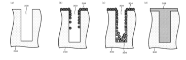
【課題】基板の凹部内に所望の厚さ分布を有する膜を形成することが可能な技術を提供する。【解決手段】(a)処理室内の基板に対して、所定元素及びハロゲン元素を含有する第1ガスを供給する工程と、(b)処理室内から第1ガスを除去する工程と、(c)(a)と(b)とを含むサイクルを第1の所定回数行うことで、基板上に、所定元素を含有し、表面がハロゲン終端された第1層を形成する工程と、(d)第1層が形成された基板に対して、所定元素を含有する第2ガスを供給することで、基板上に所定元素を含有する第2層を形成する工程と、(e)(c)と(d)とを含むサイクルを第2の所定回数行うことで、基板上に所定元素を含有する膜を形成する工程と、を有する。【選択図】図4[Problem] To provide a technology capable of forming a film having a desired thickness distribution in a recess of a substrate. [Solution] The method includes the steps of: (a) supplying a first gas containing a predetermined element and a halogen element to a substrate in a processing chamber; (b) removing the first gas from the processing chamber; (c) performing a cycle including (a) and (b) a first predetermined number of times to form a first layer on the substrate containing the predetermined element and having a halogen-terminated surface; (d) supplying a second gas containing the predetermined element to the substrate on which the first layer has been formed to form a second layer on the substrate containing the predetermined element; and (e) performing a cycle including (c) and (d) a second predetermined number of times to form a film on the substrate containing the predetermined element. [Selected Figure] Figure 4
Description
本開示は、基板処理方法、半導体装置の製造方法、プログラム、および基板処理装置に関する。 The present disclosure relates to a substrate processing method, a semiconductor device manufacturing method, a program, and a substrate processing apparatus.
半導体装置の製造工程の一工程として、成膜工程とエッチング工程とを繰り返し行って膜を形成する成膜処理が行われることがある(例えば特許文献1参照)。 As a step in the manufacturing process of a semiconductor device, a film forming process is sometimes performed in which a film is formed by repeatedly performing a film forming process and an etching process (for example, see Patent Document 1).
しかしながら、従来の処理では、例えば、表面に凹部が形成されている基板に対し、凹部内に所望の厚さ分布を有する膜を形成することが困難となる場合がある。 However, with conventional processing, for example, it can be difficult to form a film with a desired thickness distribution within a recess on a substrate that has a recess on its surface.
本開示は、例えば、基板の凹部内に所望の厚さ分布を有する膜を形成することが可能な技術を提供することにある。 The present disclosure aims to provide a technology that can form a film having a desired thickness distribution within a recess in a substrate, for example.
本開示の一態様によれば、
(a)処理室内の基板に対して、所定元素及びハロゲン元素を含有する第1ガスを供給する工程と、
(b)前記処理室内から前記第1ガスを除去する工程と、
(c)(a)と(b)とを含むサイクルを第1の所定回数行うことで、前記基板上に、前記所定元素を含有し、表面がハロゲン終端された第1層を形成する工程と、
(d)前記第1層が形成された前記基板に対して、前記所定元素を含有する第2ガスを供給することで、前記基板上に前記所定元素を含有する第2層を形成する工程と、
(e)(c)と(d)とを含むサイクルを第2の所定回数行うことで、前記基板上に前記所定元素を含有する膜を形成する工程と、
を行う技術が提供される。
According to one aspect of the present disclosure,
(a) supplying a first gas containing a predetermined element and a halogen element to the substrate in the processing chamber;
(b) removing the first gas from the processing chamber;
(c) forming a first layer containing the predetermined element and having a halogen-terminated surface on the substrate by performing a cycle including (a) and (b) a first predetermined number of times; ,
(d) forming a second layer containing the predetermined element on the substrate by supplying a second gas containing the predetermined element to the substrate on which the first layer is formed; ,
(e) forming a film containing the predetermined element on the substrate by performing a cycle including (c) and (d) a second predetermined number of times;
The technology to do this will be provided.
本開示によれば、例えば、基板の凹部内に所望の厚さ分布を有する膜を形成することが可能な技術を提供できる。 According to the present disclosure, for example, it is possible to provide a technique capable of forming a film having a desired thickness distribution within a recessed portion of a substrate.
<本開示の一態様>
以下、本開示の一態様について、主に、図1~図4、図5(a)~図5(d)を参照しつつ説明する。なお、以下の説明において用いられる図面は、いずれも模式的なものであり、図面に示される、各要素の寸法の関係、各要素の比率等は、現実のものとは必ずしも一致していない。また、複数の図面の相互間においても、各要素の寸法の関係、各要素の比率等は必ずしも一致していない。
<One aspect of the present disclosure>
Hereinafter, one embodiment of the present disclosure will be described mainly with reference to Figures 1 to 4 and 5(a) to 5(d). Note that all of the drawings used in the following description are schematic, and the dimensional relationships of the elements, the ratios of the elements, etc. shown in the drawings do not necessarily match those in reality. Furthermore, the dimensional relationships of the elements, the ratios of the elements, etc. do not necessarily match between multiple drawings.
(1)基板処理装置の構成
図1に示すように、処理炉202は温度調整器(加熱部)としてのヒータ207を有する。ヒータ207は円筒形状であり、保持板に支持されることにより垂直に据え付けられている。ヒータ207は、ガスを熱で活性化(励起)させる活性化機構(励起部)としても機能する。
(1) Configuration of the Substrate Processing Apparatus As shown in Fig. 1, the
ヒータ207の内側には、ヒータ207と同心円状に反応管203が配設されている。反応管203は、例えば石英(SiO2)または炭化シリコン(SiC)等の耐熱性材料により構成され、上端が閉塞し下端が開口した円筒形状に形成されている。反応管203の下方には、反応管203と同心円状に、マニホールド209が配設されている。マニホールド209は、例えばステンレス鋼(SUS)等の金属材料により構成され、上端および下端が開口した円筒形状に形成されている。マニホールド209の上端部は、反応管203の下端部に係合しており、反応管203を支持するように構成されている。マニホールド209と反応管203との間には、シール部材としてのOリング220aが設けられている。反応管203はヒータ207と同様に垂直に据え付けられている。主に、反応管203とマニホールド209とにより処理容器(反応容器)が構成される。処理容器の筒中空部には処理室201が形成される。処理室201は、基板としてのウエハ200を収容可能に構成されている。この処理室201内でウエハ200に対する処理が行われる。
Inside the
処理室201内には、第1供給部、第2供給部としてのノズル249a,249bが、マニホールド209の側壁を貫通するようにそれぞれ設けられている。ノズル249a,249bを、それぞれ第1ノズル、第2ノズルとも称する。ノズル249a,249bは、例えば石英またはSiC等の耐熱性材料により構成されている。ノズル249a,249bには、ガス供給管232a,232bがそれぞれ接続されている。ノズル249a,249bはそれぞれ異なるノズルであり、隣接して設けられている。
Inside the
ガス供給管232a,232bには、ガス流の上流側から順に、流量制御器(流量制御部)であるマスフローコントローラ(MFC)241a,241bおよび開閉弁であるバルブ243a,243bがそれぞれ設けられている。ガス供給管232aのバルブ243aよりも下流側には、ガス供給管232c,232dがそれぞれ接続されている。ガス供給管232bのバルブ243bよりも下流側には、ガス供給管232eが接続されている。ガス供給管232c~232eには、ガス流の上流側から順に、MFC241c~241eおよびバルブ243c~243eがそれぞれ設けられている。ガス供給管232a~232eは、例えば、SUS等の金属材料により構成されている。
The
図2に示すように、ノズル249a,249bは、反応管203の内壁とウエハ200との間における平面視において円環状の空間に、反応管203の内壁の下部より上部に沿って、ウエハ200の配列方向上方に向かって立ち上がるようにそれぞれ設けられている。すなわち、ノズル249a,249bは、ウエハ200が配列されるウエハ配列領域の側方の、ウエハ配列領域を水平に取り囲む領域に、ウエハ配列領域に沿うようにそれぞれ設けられている。ガス供給孔250a,250bは、それぞれが、平面視においてウエハ200の中心に向かって開口しており、ウエハ200に向けてガスを供給することが可能となっている。ガス供給孔250a,250bは、反応管203の下部から上部にわたって複数設けられている。
As shown in FIG. 2, the
ガス供給管232aからは、所定元素及びハロゲン元素を含有する第1ガスが、MFC241a、バルブ243a、ノズル249aを介して処理室201内へ供給される。
A first gas containing a predetermined element and a halogen element is supplied from the
ガス供給管232bからは、第1ガスが含有する所定元素と同じ所定元素を含有する第2ガスが、MFC241b、バルブ243b、ノズル249bを介して処理室201内へ供給される。
A second gas containing the same predetermined element as the first gas is supplied from the
ガス供給管232cからは、エッチングガスが、MFC241c、バルブ243c、ノズル249cを介して処理室201内へ供給される。
Etching gas is supplied from the
ガス供給管232d,232eからは、不活性ガスが、それぞれMFC241d,241e、バルブ243d,243e、ガス供給管232a,232b、ノズル249a,249bを介して処理室201内へ供給される。不活性ガスは、パージガス、キャリアガス、希釈ガス等として作用する。
Inert gas is supplied from the
主に、ガス供給管232a、MFC241a、バルブ243aにより、第1ガス供給系が構成される。主に、ガス供給管232b、MFC241b、バルブ243bにより、第2ガス供給系が構成される。主に、ガス供給管232c、MFC241c、バルブ243cにより、エッチングガス供給系が構成される。主に、ガス供給管232d,232e、MFC241d,241e、バルブ243d,243eにより、不活性ガス供給系が構成される。
A first gas supply system is mainly composed of the
第2ガスは、原料ガス(成膜ガス)として作用することから、第2ガス供給系を原料ガス(成膜ガス)供給系とも称する。また、第1ガスは、成膜阻害ガスとして作用することから、第1ガス供給系を成膜阻害ガス供給系とも称する。 Since the second gas acts as a source gas (film-forming gas), the second gas supply system is also referred to as a source gas (film-forming gas) supply system. Further, since the first gas acts as a film formation inhibiting gas, the first gas supply system is also referred to as a film formation inhibiting gas supply system.
上述の各種供給系のうち、いずれか、或いは、全ての供給系は、バルブ243a~243eやMFC241a~241e等が集積されてなる集積型供給システム248として構成されていてもよい。集積型供給システム248は、ガス供給管232a~232eのそれぞれに対して接続され、ガス供給管232a~232e内への各種物質(各種ガス)の供給動作、すなわち、バルブ243a~243eの開閉動作やMFC241a~241eによる流量調整動作等が、後述するコントローラ121によって制御されるように構成されている。集積型供給システム248は、一体型、或いは、分割型の集積ユニットとして構成されており、ガス供給管232a~232e等に対して集積ユニット単位で着脱を行うことができ、集積型供給システム248のメンテナンス、交換、増設等を、集積ユニット単位で行うことが可能なように構成されている。
Any or all of the various supply systems described above may be configured as an
反応管203の側壁下方には、処理室201内の雰囲気を排気する排気口231aが設けられている。排気口231aは、反応管203の側壁の下部より上部に沿って、すなわち、ウエハ配列領域に沿って設けられていてもよい。排気口231aには排気管231が接続されている。排気管231には、処理室201内の圧力を検出する圧力検出器(圧力検出部)としての圧力センサ245および圧力調整器(圧力調整部)としてのAPC(Auto Pressure Controller)バルブ244を介して、真空排気装置としての真空ポンプ246が接続されている。APCバルブ244は、真空ポンプ246を作動させた状態で弁を開閉することで、処理室201内の真空排気および真空排気停止を行うことができ、更に、真空ポンプ246を作動させた状態で、圧力センサ245により検出された圧力情報に基づいて弁開度を調節することで、処理室201内の圧力を調整することができるように構成されている。主に、排気管231、APCバルブ244、圧力センサ245により、排気系が構成される。真空ポンプ246を排気系に含めて考えてもよい。
An
マニホールド209の下方には、マニホールド209の下端開口を気密に閉塞可能な炉口蓋体としてのシールキャップ219が設けられている。シールキャップ219は、例えばSUS等の金属材料により構成され、円盤状に形成されている。シールキャップ219の上面には、マニホールド209の下端と当接するシール部材としてのOリング220bが設けられている。シールキャップ219の下方には、後述するボート217を回転させる回転機構267が設置されている。回転機構267の回転軸255は、例えばSUS等の金属材料により構成され、シールキャップ219を貫通してボート217に接続されている。回転機構267は、ボート217を回転させることでウエハ200を回転させるように構成されている。シールキャップ219は、反応管203の外部に設置された昇降機構としてのボートエレベータ115によって垂直方向に昇降されるように構成されている。ボートエレベータ115は、シールキャップ219を昇降させることで、ウエハ200を処理室201内外に搬入および搬出(搬送)する搬送装置(搬送機構)として構成されている。搬送装置は、処理室201内へウエハ200を提供する提供装置として機能する。
A
マニホールド209の下方には、シールキャップ219を降下させボート217を処理室201内から搬出した状態で、マニホールド209の下端開口を気密に閉塞可能な炉口蓋体としてのシャッタ219sが設けられている。シャッタ219sは、例えばSUS等の金属材料により構成され、円盤状に形成されている。シャッタ219sの上面には、マニホールド209の下端と当接するシール部材としてのOリング220cが設けられている。シャッタ219sの開閉動作(昇降動作や回動動作等)は、シャッタ開閉機構115sにより制御される。
A
基板支持具としてのボート217は、複数枚、例えば25~200枚のウエハ200を、水平姿勢で、かつ、互いに中心を揃えた状態で鉛直方向に整列させて多段に支持するように、すなわち、間隔を空けてウエハ200の面に対して垂直方向に配列させるように構成されている。ボート217は、例えば石英やSiC等の耐熱性材料により構成される。ボート217の下部には、例えば石英やSiC等の耐熱性材料により構成される断熱板218が多段に支持されている。
The
反応管203内には、温度検出器としての温度センサ263が設置されている。温度センサ263により検出された温度情報に基づきヒータ207への通電具合を調整することで、処理室201内の温度が所望の温度分布となる。温度センサ263は、反応管203の内壁に沿って設けられている。
A
図3に示すように、制御部(制御手段)であるコントローラ121は、CPU(Central Processing Unit)121a、RAM(Random Access Memory)121b、記憶装置121c、I/Oポート121dを備えたコンピュータとして構成されている。RAM121b、記憶装置121c、I/Oポート121dは、内部バス121eを介して、CPU121aとデータ交換可能なように構成されている。コントローラ121には、例えばタッチパネル等として構成された入出力装置122が接続されている。また、コントローラ121には、外部記憶装置123を接続することが可能となっている。
As shown in FIG. 3, the
記憶装置121cは、例えばフラッシュメモリ、HDD(Hard Disk Drive)、SSD(Solid State Drive)等で構成されている。記憶装置121c内には、基板処理装置の動作を制御する制御プログラムや、後述する基板処理の手順や条件等が記載されたプロセスレシピ等が、読み出し可能に記録され、格納されている。プロセスレシピは、後述する基板処理における各手順をコントローラ121によって、基板処理装置に実行させ、所定の結果を得ることができるように組み合わされたものであり、プログラムとして機能する。以下、プロセスレシピや制御プログラム等を総称して、単に、プログラムともいう。また、プロセスレシピを、単に、レシピともいう。本明細書においてプログラムという言葉を用いた場合は、レシピ単体のみを含む場合、制御プログラム単体のみを含む場合、または、それらの両方を含む場合がある。RAM121bは、CPU121aによって読み出されたプログラムやデータ等が一時的に保持されるメモリ領域(ワークエリア)として構成されている。
The
I/Oポート121dは、上述のMFC241a~241e、バルブ243a~243e、圧力センサ245、APCバルブ244、真空ポンプ246、温度センサ263、ヒータ207、回転機構267、ボートエレベータ115、シャッタ開閉機構115s等に接続されている。
The I/
CPU121aは、記憶装置121cから制御プログラムを読み出して実行すると共に、入出力装置122からの操作コマンドの入力等に応じて記憶装置121cからレシピを読み出すことが可能なように構成されている。CPU121aは、読み出したレシピの内容に沿うように、MFC241a~241eによる各種物質(各種ガス)の流量調整動作、バルブ243a~243eの開閉動作、APCバルブ244の開閉動作および圧力センサ245に基づくAPCバルブ244による圧力調整動作、真空ポンプ246の起動および停止、温度センサ263に基づくヒータ207の温度調整動作、回転機構267によるボート217の回転および回転速度調節動作、ボートエレベータ115によるボート217の昇降動作、シャッタ開閉機構115sによるシャッタ219sの開閉動作等を制御することが可能なように構成されている。
The
コントローラ121は、外部記憶装置123に記録され、格納された上述のプログラムを、コンピュータにインストールすることにより構成することができる。外部記憶装置123は、例えば、HDD等の磁気ディスク、CD等の光ディスク、MO等の光磁気ディスク、USBメモリやSSD等の半導体メモリ等を含む。記憶装置121cや外部記憶装置123は、コンピュータ読み取り可能な記録媒体として構成されている。以下、これらを総称して、単に、記録媒体ともいう。本明細書において記録媒体という言葉を用いた場合は、記憶装置121c単体のみを含む場合、外部記憶装置123単体のみを含む場合、または、それらの両方を含む場合がある。なお、コンピュータへのプログラムの提供は、外部記憶装置123を用いず、インターネットや専用回線等の通信手段を用いて行ってもよい。
The
(2)基板処理工程
上述の基板処理装置を用い、半導体装置の製造工程の一工程として、基板としてのウエハ200上に膜を形成する処理シーケンスの例について、主に、図4、図5(a)~図5(d)を用いて説明する。本態様では、一例として、ウエハ200の表面に、凹部300が形成されている場合について説明する。本明細書において「凹部」とは、トレンチやホールだけでなく、横穴や貫通孔等、開口に対して内部の表面積が大きい構造全般を含むものとする。なお、以下の説明において、基板処理装置100を構成する各部の動作は、コントローラ121により制御される。
(2) Substrate processing process An example of a processing sequence for forming a film on a
本態様における処理シーケンスでは、
処理室201内のウエハ200に対して、所定元素及びハロゲン元素を含有する第1ガスを供給するステップAと、
処理室201内から第1ガスを除去するステップBと、
ステップAとステップBとを含むサイクルを第1の所定回数(n回、nは1以上の整数)行うことで、ウエハ200上に、所定元素を含有し、表面がハロゲン終端された第1層304を形成するステップCと、
第1層304が形成されたウエハ200に対して、所定元素を含有する第2ガスを供給することで、ウエハ200上に所定元素を含有する第2層306を形成するステップDと、
ステップCとステップDとを含むサイクルを第2の所定回数(m回、mは1以上の整数)行うことで、ウエハ200上に所定元素を含有する膜308を形成するステップEと、
を行う。なお、図4に記載されているA~Eは、それぞれステップA~Eを示している。
In the processing sequence in this aspect,
Step A of supplying a first gas containing a predetermined element and a halogen element to the
Step B of removing the first gas from inside the
By performing a cycle including step A and step B a first predetermined number of times (n times, n is an integer of 1 or more), a first layer containing a predetermined element and whose surface is halogen-terminated is formed on the
Step D of forming a
Step E of forming a
I do. Note that A to E shown in FIG. 4 indicate steps A to E, respectively.
なお、以下では、膜308としてシリコン(Si)膜を形成する例について説明する。
Note that an example in which a silicon (Si) film is formed as the
本明細書では、上述の処理シーケンスを、便宜上、以下のように示すこともある。以下の変形例や他の態様等の説明においても、同様の表記を用いる。 In this specification, the above-mentioned processing sequence may be expressed as follows for convenience. Similar notations will be used in the following description of modified examples and other aspects.
[(第1ガス→パージ)×n→第2ガス]×m [(First gas → purge) x n → Second gas] x m
また、図4や以下に示す処理シーケンスのように、第2ガスを供給するステップを行った後に、パージを行うステップをさらに行うようにしてもよい。本態様では、一例として、この場合について説明する。 Furthermore, as in the processing sequence shown in FIG. 4 and below, after the step of supplying the second gas is performed, a step of purging may be further performed. In this aspect, this case will be described as an example.
[(第1ガス→パージ)×n→第2ガス→パージ]×m [(First gas → purge) x n → Second gas → purge] x m
本明細書において用いる「ウエハ」という用語は、ウエハそのものを意味する場合や、ウエハとその表面に形成された所定の層や膜との積層体を意味する場合がある。本明細書において用いる「ウエハの表面」という言葉は、ウエハそのものの表面を意味する場合や、ウエハ上に形成された所定の層等の表面を意味する場合がある。本明細書において「ウエハ上に所定の層を形成する」と記載した場合は、ウエハそのものの表面上に所定の層を直接形成することを意味する場合や、ウエハ上に形成されている層等の上に所定の層を形成することを意味する場合がある。本明細書において「基板」という言葉を用いた場合も、「ウエハ」という言葉を用いた場合と同義である。 The term "wafer" used in this specification may mean the wafer itself, or a laminate of the wafer and a predetermined layer or film formed on the surface of the wafer. The term "wafer surface" used in this specification may mean the surface of the wafer itself, or the surface of a predetermined layer formed on the wafer. In this specification, when the expression "forming a predetermined layer on a wafer" refers to forming a predetermined layer directly on the surface of the wafer itself, or a layer formed on the wafer, etc. Sometimes it means forming a predetermined layer on top of. In this specification, when the word "substrate" is used, it has the same meaning as when the word "wafer" is used.
(ウエハチャージおよびボートロード)
複数枚のウエハ200がボート217に装填(ウエハチャージ)されると、シャッタ開閉機構115sによりシャッタ219sが移動させられて、マニホールド209の下端開口が開放される(シャッタオープン)。その後、図1に示すように、複数枚のウエハ200を支持したボート217は、ボートエレベータ115によって持ち上げられて処理室201内へ搬入(ボートロード)される。この状態で、シールキャップ219は、Oリング220bを介してマニホールド209の下端をシールした状態となる。
(wafer charge and boat load)
When a plurality of
ウエハ200としては、例えば、単結晶シリコン(Si)ウエハを用いることができる。また、ウエハ200の表面には、図5(a)~図5(d)に示すように、凹部300が設けられている。凹部300内の表面(最表面)、すなわち、凹部300の内壁の表面の材質は特に制限はなく、例えば、単結晶Si(単結晶Siウエハそのもの)、シリコン膜(Si膜)、ゲルマニウム膜(Ge膜)、シリコンゲルマニウム膜(SiGe膜)、シリコン炭化膜(SiC膜)、シリコン窒化膜(SiN膜)、シリコン炭窒化膜(SiCN膜)、シリコン酸化膜(SiO膜)シリコン酸窒化膜(SiON)、シリコン酸炭化膜(SiOC膜)、シリコン酸炭窒化膜(SiOCN膜)、シリコン硼窒化膜(SiBN膜)、シリコン硼炭窒化膜(SiBCN膜)、硼窒化膜(BN膜)等が挙げられ、例えば、これらのうち少なくともいずれか1つである場合がある。
For example, a single crystal silicon (Si) wafer can be used as the
(圧力調整および温度調整)
ボートロードが終了した後、処理室201内、すなわち、ウエハ200が存在する空間が所望の圧力(真空度)となるように、真空ポンプ246によって真空排気(減圧排気)される。この際、処理室201内の圧力は圧力センサ245で測定され、この測定された圧力情報に基づきAPCバルブ244がフィードバック制御される。また、処理室201内のウエハ200が所望の処理温度となるように、ヒータ207によって加熱される。この際、処理室201内が所望の温度分布となるように、温度センサ263が検出した温度情報に基づきヒータ207への通電具合がフィードバック制御される。また、回転機構267によるウエハ200の回転を開始する。処理室201内の排気、ウエハ200の加熱および回転は、いずれも、少なくともウエハ200に対する処理が終了するまでの間は継続して行われる。
(Pressure and temperature regulation)
After the boat loading is completed, the inside of the
その後、ステップA~Eをこの順に実行し、ウエハ200上への成膜処理を行う。本明細書では、ウエハ200の表面に設けられた凹部300内への成膜処理を、埋め込み処理とも称する。以下、これらの各ステップについて説明する。
Thereafter, steps A to E are executed in this order to form a film on the
[ステップA]
ステップAでは、処理室201内のウエハ200に対して第1ガスを供給する。
[Step A]
In step A, a first gas is supplied to the
具体的には、バルブ243aを開き、ガス供給管232a内へ第1ガスを流す。第1ガスは、MFC241aにより流量調整され、ノズル249aを介して処理室201内へ供給され、排気口231aより排気される。このとき、ウエハ200に対して第1ガスが供給される(第1ガス供給)。このとき、バルブ243d,243eを開き、ノズル249a,249bのそれぞれを介して処理室201内へ不活性ガスを供給するようにしてもよい。
Specifically, the
本ステップにおける処理条件としては、
処理温度:300~600℃、好ましくは400~500℃
処理圧力:1k~100kPa、好ましくは20k~50kPa
第1ガス供給流量:0.1~1slm、好ましくは0.2~0.5slm
第1ガス供給時間:1~10分、好ましくは3~6分
不活性ガス供給流量(ガス供給管毎):0~0.5slm
が例示される。
The processing conditions in this step are:
Processing temperature: 300-600°C, preferably 400-500°C
Processing pressure: 1k to 100kPa, preferably 20k to 50kPa
First gas supply flow rate: 0.1 to 1 slm, preferably 0.2 to 0.5 slm
First gas supply time: 1 to 10 minutes, preferably 3 to 6 minutes Inert gas supply flow rate (for each gas supply pipe): 0 to 0.5 slm
is exemplified.
なお、本明細書における「300~600℃」のような数値範囲の表記は、下限値および上限値がその範囲に含まれることを意味する。よって、例えば、「300~600℃」とは「300℃以上600℃以下」を意味する。他の数値範囲についても同様である。また、本明細書における処理温度とはウエハ200の温度または処理室201内の温度のことを意味し、処理圧力とは処理室201内の圧力のことを意味する。また、供給流量に0slmが含まれる場合、0slmとは、そのガスを供給しないケースを意味する。これらは、以下の説明においても同様である。
Note that the notation of a numerical range such as "300 to 600°C" in this specification means that the lower limit and upper limit are included in the range. Therefore, for example, "300 to 600°C" means "300°C or more and 600°C or less". The same applies to other numerical ranges. Further, in this specification, the processing temperature means the temperature of the
上述の条件下でウエハ200に対して、第1ガスとして、例えば、所定元素としてのSiとハロゲン元素としての塩素(Cl)とを含み、Si-Cl結合を有するクロロシラン系ガスを供給することにより、当該ガスの分子に含まれるSi-Cl結合の一部をウエハ200の表面と反応させ、当該ガスをウエハ200の表面に吸着させることができる。また、上述の条件下では、ウエハ200の表面に吸着した第1ガスの分子に含まれるSi-Cl結合であって、ウエハ200の表面と反応しなかった残りのSi-Cl結合をそのまま保持させ、ウエハ200の表面にハロゲン終端であるCl終端(Si-Cl終端)を形成することができる。なお、第1ガスのウエハ200の表面への吸着は、未結合手を有することとなったSiが表面と反応することによって化学吸着する場合のほかに、Si-Cl結合を保持した第1ガスが表面に物理吸着する場合を含んでいてもよい。
By supplying the
ウエハ200の表面に第1ガスを吸着させた後、バルブ243aを閉じ、処理室201内への第1ガスの供給を停止する。
After the first gas is adsorbed onto the surface of the
第1ガスとしては、例えば、所定元素としてのSiとハロゲン元素とを含むハロシラン系ガスを用いることができる。ハロゲンには、例えば、Cl、フッ素(F)、臭素(Br)、ヨウ素(I)等が含まれる。ハロシラン系ガスとしては、例えば、SiおよびClを含む上述のクロロシラン系ガスを用いることができる。 As the first gas, for example, a halosilane gas containing Si as a predetermined element and a halogen element can be used. Examples of halogen include Cl, fluorine (F), bromine (Br), and iodine (I). As the halosilane gas, for example, the above-mentioned chlorosilane gas containing Si and Cl can be used.
第1ガスとしては、例えば、ジクロロシラン(SiH2Cl2、略称:DCS)ガス、テトラクロロシラン(SiCl4、略称:STC)ガス、ヘキサクロロジシランガス(Si2Cl6、略称:HCDS)ガス、オクタクロロトリシラン(Si3Cl8、略称:OCTS)ガス等のクロロシラン系ガスを用いることができる。第1ガスとしては、これらのうち1以上を用いることができる。 Examples of the first gas include dichlorosilane (SiH 2 Cl 2 , abbreviation: DCS) gas, tetrachlorosilane (SiCl 4 , abbreviation: STC) gas, hexachlorodisilane gas (Si 2 Cl 6 , abbreviation: HCDS) gas, octachlorosilane (SiCl 4 , abbreviation: HCDS) gas, A chlorosilane-based gas such as chlorotrisilane (Si 3 Cl 8 , abbreviation: OCTS) gas can be used. One or more of these can be used as the first gas.
第1ガスとしては、クロロシラン系ガスの他、テトラフルオロシラン(SiF4)ガス、ジフルオロシラン(SiH2F2)ガス、ヘキサフルオロジシラン(Si2F6、略称:HFDS)ガス、オクタフルオロトリシラン(Si3F8)ガス等のフルオロシラン系ガスや、テトラブロモシラン(SiBr4)ガス等のブロモシラン系ガス、ヘキサブロモジシラン(Si2Br6、略称:HBDS)ガス、オクタブロモトリシラン(Si3Br8)ガス等のブロモシラン系ガスや、テトラヨードシラン(SiI4、略称:STI)ガス、ジヨードシラン(SiH2I2)ガス、ヘキサヨードジシラン(Si2I6、略称:HIDS)ガス、オクタヨードトリシラン(Si3I8)ガス等のヨードシラン系ガスを用いることもできる。第1ガスとしては、これらのうち1以上を用いることができる。 In addition to chlorosilane gas, the first gas includes tetrafluorosilane (SiF 4 ) gas, difluorosilane (SiH 2 F 2 ) gas, hexafluorodisilane (Si 2 F 6 , abbreviation: HFDS) gas, and octafluorotrisilane. (Si 3 F 8 ) gas, bromosilane gas such as tetrabromosilane (SiBr 4 ) gas, hexabromodisilane (Si 2 Br 6 , abbreviation: HBDS) gas, octabromotrisilane (Si Bromosilane gas such as Br 3 Br 8 ) gas, tetraiodosilane (SiI 4 , abbreviation: STI) gas, diiodosilane (SiH 2 I 2 ) gas, hexaiododisilane (Si 2 I 6 , abbreviation: HIDS) gas, octa-silane gas, etc. Iodosilane gas such as iodotrisilane (Si 3 I 8 ) gas can also be used. One or more of these can be used as the first gas.
不活性ガスとしては、例えば、窒素(N2)ガスや、アルゴン(Ar)ガス、ヘリウム(He)ガス、ネオン(Ne)ガス、キセノン(Xe)ガス等の希ガスを用いることができる。不活性ガスとしては、これらのうち1以上を用いることができる。この点は、後述する各ステップにおいても同様である。 As the inert gas, for example, a rare gas such as nitrogen (N 2 ) gas, argon (Ar) gas, helium (He) gas, neon (Ne) gas, or xenon (Xe) gas can be used. One or more of these can be used as the inert gas. This point also applies to each step described below.
[ステップB]
ステップBでは、処理室201内を真空排気し、処理室201内に残留するガス状物質等を処理室201内から排除する。このとき、処理室201内へ不活性ガスを供給する。
[Step B]
In Step B, the inside of the
具体的には、バルブ243d,243eを開き、ガス供給管232a,232b内へ不活性ガスを流す。不活性ガスは、MFC241d,241eにより流量調整され、ノズル249a,249bを介して処理室201内へ供給され、排気口231aより排気される。ノズル249a,249bより供給される不活性ガスは、パージガスとして作用し、これにより、処理室201内がパージされる(パージ)。
Specifically, the
本ステップにおける処理条件としては、
処理圧力:10~100Pa
不活性ガス供給流量(ガス供給管毎):0.1~1slm
不活性ガス供給時間:1~120秒、好ましくは1~60秒
が例示される。他の処理条件は、ステップAにおける処理条件と同様な処理条件とする。
The processing conditions in this step are:
Processing pressure: 10-100Pa
Inert gas supply flow rate (for each gas supply pipe): 0.1 to 1 slm
Inert gas supply time: 1 to 120 seconds, preferably 1 to 60 seconds. Other processing conditions are similar to those in step A.
[ステップC(サイクルの所定回数実施)]
上述のステップA,Bを非同時に、すなわち、同期させることなく行うサイクルを第1の所定回数(n回、nは1以上の整数)行うことにより、下地としてのウエハ200の最表面上に、第1層304として、例えば表面がハロゲン終端(Cl終端)された所定元素(Si)を含有する層が形成される。
[Step C (Implementing the cycle a predetermined number of times)]
By performing a cycle in which steps A and B described above are performed non-simultaneously, that is, without synchronization, for a first predetermined number of times (n times, n is an integer of 1 or more), on the outermost surface of the
本ステップでは、例えば、凹部300内面の一部における第1層304の密度を、凹部300内面の他の部分における第1層304の密度よりも高くすることができる。具体的には、例えば、1サイクル当たりの第1ガスの供給流量を少くすることや、第1ガスの供給時間を短くすることにより、第1ガスが、凹部300内面の底部近傍に到達することを抑制し、第1ガスの供給が凹部300内面の開口部近傍に対して限定されるようにする。こうすることにより、例えば、開口部近傍における第1層304の密度を、底部近傍における第1層304の密度よりも高くすることが容易となる(図5(b)参照)。このとき、第1の所定回数を2回以上、すなわち、上述のサイクルを2回以上行うことにより、この第1層304の密度の調整をさらに容易に行うことができる。本明細書において、凹部300内面における「層の密度」とは、例えば、凹部300内面における単位面積当たりの、Cl等が結合している(すなわちCl等で終端されている)Si等の吸着個数、または凹部300内面における単位面積当たりの層の平均的な厚さと同義であると考えることもできる。
In this step, for example, the density of the
さらに、本ステップでは、1サイクル当たりのステップAの実行時間(第1ガスの供給時間)や第1ガス供給流量を調整することにより、凹部300内面の開口部近傍に形成される第1層304の密度に対する底部近傍に形成される第1層304の密度の割合を所望の大きさとすることができる。具体的には、例えば、1サイクル当たりのステップAの実行時間を所定の時間から短くする方向に調整することや、ステップAにおける第1ガスの供給流量を所定の流量から減少させる方向に調整することにより、凹部300内面の開口部近傍に形成される第1層304の密度に対する底部近傍に形成される第1層304の密度の割合を小さくするように制御することができる。
Furthermore, in this step, the
[ステップD]
ステップDでは、処理室201内のウエハ200に対して第2ガスを供給する。
[Step D]
In step D, a second gas is supplied to the
具体的には、バルブ243bを開き、ガス供給管232b内へ第2ガスを流す。第1ガスは、MFC241bにより流量調整され、ノズル249bを介して処理室201内へ供給され、排気口231aより排気される。このとき、ウエハ200に対して第2ガスが供給される(第2ガス供給)。このとき、バルブ243d,243eを開き、ノズル249a,249bのそれぞれを介して処理室201内へ不活性ガスを供給するようにしてもよい。
Specifically, the
本ステップにおける処理条件としては、
処理温度:400~600℃、好ましくは450~550℃
処理圧力:10~500Pa、好ましくは50~100Pa
第2ガス供給流量:1~5slm、好ましくは2~4slm
第2ガス供給時間:10~120分、好ましくは30~90分
が例示される。他の処理条件は、ステップAにおける処理条件と同様な処理条件とする。
The processing conditions in this step are:
Processing temperature: 400-600°C, preferably 450-550°C
Processing pressure: 10 to 500 Pa, preferably 50 to 100 Pa
Second gas supply flow rate: 1 to 5 slm, preferably 2 to 4 slm
Second gas supply time: 10 to 120 minutes, preferably 30 to 90 minutes. Other processing conditions are similar to those in step A.
上述の条件下でウエハ200に対して、第2ガスとして、例えば、所定元素としてのSiを含むシラン系ガスを供給することにより、ウエハ200上に、第2層306としてのSi含有層が形成される。具体的には、例えば、凹部300内面において、第2層306は、開口部近傍における密度が、底部近傍における密度よりも低くなるように形成される(図5(c)参照)。第2層306が、このような密度分布で形成されるのは、第1層304の表面に存在するCl終端が、第2ガスに含まれるSi原子の第1層304の表面への吸着を阻害する要因、すなわち、インヒビターとして作用するためである。
Under the above-mentioned conditions, a silane-based gas containing Si as a specific element is supplied as the second gas to the
第2層が形成された後、バルブ243bを閉じ、処理室201内への第2ガスの供給を停止する。そして、ステップBにおけるパージと同様の処理手順、処理条件により、処理室201内に残留するガス状物質等を処理室201内から排除する(パージ)。
After the second layer is formed, the
第2ガスとしては、例えば、ウエハ200上に形成される膜を構成する主元素としてのSiを含む上述のシラン系ガスを用いることができる。シラン系ガスとしては、例えば、モノシラン(SiH4)ガス、ジシラン(Si2H6)ガス等のSiを含有しハロゲンを非含有とするガスを用いることができる。第2ガスとしては、これらのうち1以上を用いることができる。
As the second gas, for example, the above-mentioned silane gas containing Si as the main element constituting the film formed on the
[ステップE(成膜処理・サイクルの所定回数実施)]
上述のステップC,Dを非同時に、すなわち、同期させることなく行うサイクルを第2の所定回数(m回、mは1以上の整数)行うことにより、ウエハ200上に、第2層306が積層されてなる膜308として、例えばSi膜が形成される。上述したように、例えば、凹部300内面において、インヒビター効果を有する第1層304は、開口部近傍における密度が、底部近傍における密度よりも高いので、膜308は、凹部300内面の底部から開口部に向けてボトムアップ成長し、凹部300内を膜308により埋め込むことができる(図5(d)参照)。これにより、凹部300内にボイドフリーかつシームレスな膜308を形成でき、埋め込み特性を向上させることができる。
[Step E (film formation process/cycle performed a predetermined number of times)]
The
上述のステップDでは、例えば、第1層304の表面に存在するCl終端におけるCl原子(ハロゲン原子)の少なくとも一部が、第1層304の表面から脱離することがある。これにより、第1層304のインヒビター効果が不充分となり、膜308のボトムアップ成長が阻害される場合がある。このとき、第2の所定回数を2回以上、すなわち、上述のサイクルを2回以上行うことにより、表面がCl終端された第1層304を再度形成できる。これにより、第1層304のインヒビター効果を維持することができ、膜308のボトムアップ成長を継続することができる。これにより、凹部300内にボイドフリーかつシームレスな膜308を形成でき、埋め込み特性を向上させることができる。なお、ステップDにおいて第1層304の表面からCl原子(ハロゲン原子)が脱離した場合、脱離したCl原子と結合していた第1層304を構成するSi原子(所定元素の原子)は、そのまま膜308を構成するSi原子(所定元素の原子)と見做すことができる。
In step D described above, for example, at least a portion of the Cl atoms (halogen atoms) at the Cl terminations present on the surface of the
上述のステップDを、例えば、第2ガスが気相分解(熱分解)する条件下で行うことにより、第2ガスに含まれるSiをウエハ200上に多重に堆積させる。これにより、膜308の形成速度を向上させることができる。
By performing the above-mentioned step D under conditions in which the second gas undergoes gas-phase decomposition (thermal decomposition), for example, the Si contained in the second gas is deposited in multiple layers on the
(アフターパージおよび大気圧復帰)
ステップEが終了したら、ノズル249a,249bのそれぞれからパージガスとしての不活性ガスを処理室201内へ供給し、排気口231aより排気する。これにより、処理室201内がパージされ、処理室201内に残留するガスや反応副生成物等が処理室201内から除去される(アフターパージ)。その後、処理室201内の雰囲気が不活性ガスに置換され(不活性ガス置換)、処理室201内の圧力が常圧に復帰される(大気圧復帰)。
(After purge and return to atmospheric pressure)
When step E is completed, inert gas as a purge gas is supplied into the
(ボートアンロードおよびウエハディスチャージ)
その後、ボートエレベータ115によりシールキャップ219が下降され、マニホールド209の下端が開口される。そして、処理済のウエハ200が、ボート217に支持された状態でマニホールド209の下端から反応管203の外部に搬出(ボートアンロード)される。ボートアンロードの後は、シャッタ219sが移動させられ、マニホールド209の下端開口がOリング220cを介してシャッタ219sによりシールされる(シャッタクローズ)。処理済のウエハ200は、反応管203の外部に搬出された後、ボート217より取り出される(ウエハディスチャージ)。
(Boat unloading and wafer discharge)
Thereafter, the
(3)本態様による効果
本態様によれば、以下に示す1つ又は複数の効果が得られる。
(3) Effects of this aspect According to this aspect, one or more of the following effects can be obtained.
(a)第1層304の表面に存在するCl終端は、第2層306の形成を阻害するインヒビターとして作用するので、例えば、ウエハ200の表面に凹部300が形成されている場合には、凹部300内の第1層304の密度分布を調整することにより、第2層306の厚さ分布を制御できる。結果として、凹部300内に所望の厚さ分布の膜308を形成することが可能となる。
(a) Since the Cl termination present on the surface of the
第1ガスが第2ガスと同様にSiを含むので、第1ガスがSiを含まない場合と比べて、膜308の形成速度を向上させることが可能となる。
Since the first gas contains Si like the second gas, it is possible to improve the formation rate of the
(b)ステップCでは、凹部300内面おいて、第1層304の密度が、開口部近傍の方が底部近傍よりも高くなっているので、膜308は、凹部300内面の底部から開口部に向けてボトムアップ成長し、凹部300内を膜308により埋め込むことができる。これにより、凹部300内にボイドフリーかつシームレスな膜308を形成でき、埋め込み特性を向上させることができる。
(b) In step C, on the inner surface of the
(c)第1ガスとして、H非含有ガスを用いることにより、ウエハ200上に、表面がH終端された層が形成されることを抑制することができる。H終端におけるH原子は、例えば、Cl終端におけるCl原子と比べて層から脱離しやすいため、ウエハ200上に、表面がH終端された層が形成された場合には、第1層304におけるインヒビター効果を発揮させることが困難となることがある。第1ガスとして、H非含有ガスを用いることにより、表面がH終端された層が形成されることを抑制することができるので、第1層304におけるインヒビター効果を充分に発揮させることができる。
(c) By using an H-free gas as the first gas, it is possible to suppress the formation of a layer on the
(d)第1ガスとして、1分子中にSi原子同士の結合(Si-Si結合)を含まないガスを用いることにより、第1ガスがステップAにおいて熱分解することを抑制できる。第1ガスが熱分解した場合には、ステップAにおいて、第1ガスに含まれ、かつウエハ200に吸着したSiが、未結合手を有する状態となりやすい。ステップDでは、この未結合手に第2ガスに含まれるSiが結合し得るので、第1層304のインヒビター効果が発揮できない場合がある。第1ガスとして、1分子中にSi原子同士の結合を含まないガスを用いることにより、第1層304のインヒビター効果を充分に発揮させることができる。
(d) By using a gas that does not contain bonds between Si atoms (Si--Si bonds) in one molecule as the first gas, thermal decomposition of the first gas in step A can be suppressed. When the first gas is thermally decomposed, Si contained in the first gas and adsorbed to the
(e)ステップCの後、少なくともステップDを開始するまでの間、ウエハ200に対して、Cl終端と反応する、第1ガス及び第2ガスのいずれのガスとも異なるガスの供給を不実施とすることにより、第1層304の表面に存在するCl終端におけるCl原子の脱離を抑制できる。これにより、第1層304は、表面におけるCl終端の存在を維持するので、ステップDにおいてインヒビター効果を発揮することができる。
(e) After step C, at least until the start of step D, a gas different from either the first gas or the second gas, which reacts with the Cl termination, is not supplied to the
(4)変形例
本態様における基板処理シーケンスは、以下に示す変形例のように変更することができる。これらの変形例は、任意に組み合わせることができる。特に説明がない限り、各変形例の各ステップにおける処理手順、処理条件は、上述の基板処理シーケンスの各ステップにおける処理手順、処理条件と同様とすることができる。
(4) Modifications The substrate processing sequence in this embodiment can be modified as in the following modifications. These modifications can be combined arbitrarily. Unless otherwise specified, the processing procedure and processing conditions in each step of each modification may be the same as the processing procedure and processing conditions in each step of the substrate processing sequence described above.
(変形例1)
以下に示す処理シーケンスのように、成膜処理(ステップE)を行った後に、ウエハ200に対して膜308をエッチング可能なエッチングガスを供給する処理(ステップF)を行い、さらにステップEを行うようにしてもよい。以下に示すp,qは、いずれも1以上の整数を示している。
(Modification 1)
As in the processing sequence shown below, after the film formation process (step E) is performed, the process of supplying an etching gas capable of etching the
[(第1ガス→パージ)×n→第2ガス→パージ]×m→エッチングガス→[(第1ガス→パージ)×p→第2ガス→パージ]×q [(1st gas → purge) × n → 2nd gas → purge] × m → etching gas → [(1st gas → purge) × p → 2nd gas → purge] × q
[ステップF]
ステップFでは、処理室201内のウエハ200に対して膜308をエッチングする作用を有するエッチングガスを供給し、膜308の一部をエッチング(除去)する。
[Step F]
In Step F, an etching gas having an effect of etching the
具体的には、バルブ243cを開き、ガス供給管232c内へエッチングガスを流す。エッチングガスは、MFC241cにより流量調整され、ノズル249aを介して処理室201内へ供給され、排気口231aより排気される。このとき、ウエハ200に対してエッチングガスが供給される(エッチングガス供給)。このとき、バルブ243d,243eを開き、ノズル249a,249bのそれぞれを介して処理室201内へ不活性ガスを供給するようにしてもよい。
Specifically, the
本ステップにおける処理条件としては、
処理温度:200~800℃、好ましくは300~600℃
処理圧力:10~100kPa、好ましくは100~50kPa
エッチングガス供給流量:0.01~10slm、好ましくは0.1~5slm
エッチングガス供給時間:1~60分、好ましくは10~30分
が例示される。他の処理条件は、ステップAにおける処理条件と同様な処理条件とする。
The processing conditions in this step are:
Processing temperature: 200-800°C, preferably 300-600°C
Processing pressure: 10-100kPa, preferably 100-50kPa
Etching gas supply flow rate: 0.01 to 10 slm, preferably 0.1 to 5 slm
Etching gas supply time: 1 to 60 minutes, preferably 10 to 30 minutes. Other processing conditions are similar to those in step A.
エッチングガスとしては、例えば、塩素(Cl2)ガス、フッ素(F2)ガス、三フッ化塩素(ClF3)ガス、塩化水素(HCl)ガス、フッ化水素(HF)ガス等のハロゲン含有ガスを用いることができる。エッチングガスとしては、これらのうち1以上を用いることができる。 Etching gases include, for example, halogen-containing gases such as chlorine (Cl 2 ) gas, fluorine (F 2 ) gas, chlorine trifluoride (ClF 3 ) gas, hydrogen chloride (HCl) gas, and hydrogen fluoride (HF) gas. can be used. One or more of these can be used as the etching gas.
本変形例においても、上述の態様と同様の効果が得られる。 This modified example also provides the same effects as the above-mentioned embodiment.
ステップCとステップDとを含むサイクルを繰り返すことにより、凹部300の内部が膜308によって完全に埋め込まれる前に、凹部300の開口部近傍が膜308によって塞がれてしまう、いわゆるオーバーハング状態となる場合がある。このとき、凹部300内に深さ方向に伸びるボイドやシームが発生してしまう場合がある。本変形例において、上述の条件下でウエハ200に対して、エッチングガスを供給することにより、凹部300内の開口部近傍に形成された膜308の一部を優先的に(選択的に)除去することができる。これにより、例えば、凹部300内に埋め込まれた膜308中にボイドやシームが形成される前に、オーバーハング状態を解消させて、ステップCとステップDとを含むサイクルを継続させることができる。また、例えば、凹部300内に埋め込まれた膜308中にボイドやシームが形成された場合に、これらを消失させることができる。膜308中に形成されたボイドやシームを消失させた後、さらに、ステップEを行うことにより、凹部300内にボイドフリーかつシームレスな膜308を確実に形成し、埋め込み特性をさらに向上させることができる。
By repeating the cycle including step C and step D, a so-called overhang state occurs in which the vicinity of the opening of the
また、ステップEを行った後にステップFを行い、その後さらにステップEを行うサイクルを複数回行うようにしてもよい。これにより、凹部300内にボイドフリーかつシームレスな膜308をさらに確実に形成し、埋め込み特性をまたさらに向上させることができる。
Alternatively, a cycle in which step E is performed, step F is performed, and step E is then further performed may be performed a plurality of times. Thereby, a void-free and
(変形例2)
ステップEでは、凹部300内面の底部近傍に対して膜308を形成するステップCおよびステップDのサイクル中での第1の所定回数よりも、凹部300内面の開口部近傍に対して膜308を形成するステップCおよびステップDのサイクル中での第1の所定回数の方を少なくしてもよい。
凹部300の内部における成膜処理(埋め込み処理)が進行すると、凹部300のアスペクト比(凹部の深さ/凹部の幅)が次第に小さくなるため、凹部300の底部から開口部にかけて高密度に第1層304が形成されやすくなる。これにより、凹部300内の全域で第2層306の形成速度が低下して、埋め込み処理の生産性が低下する場合がある。また、凹部300の底部から開口部にかけて高密度に第1層304が形成された状態で行われる埋め込み処理では、開口部近傍における膜308の厚さが、底部近傍における膜308の厚さより大きくなることがあり、凹部300内にボイド等が発生し、埋め込み処理の生産性が低下する場合がある。本変形例において、凹部300内面の底部近傍に対する膜308形成時、例えば、埋め込み処理の初期(ステップEにおける最初の所定サイクル数の間)におけるサイクルでの第1の所定回数よりも、凹部300内面の開口部近傍に対する膜308形成時、例えば、埋め込み処理の中期または終期(ステップEにおける最後の所定サイクル数の間)におけるサイクルでの第1の所定回数の方を少なくすることにより、第1層304を凹部300内面に所望な密度分布で形成できる。これにより、膜308の埋め込み特性を向上させることができる。
なお、埋め込み処理の進行時期に伴い、ステップCにおける1サイクル当たりの第1ガスの供給流量を少なくすることや、第1ガスの供給時間を短くすることでも同様の効果を得ることができる。
(Modification 2)
In step E, the
As the film forming process (embedding process) inside the
Note that the same effect can be obtained by reducing the supply flow rate of the first gas per cycle in step C or shortening the supply time of the first gas as the embedding process progresses.
<本開示の他の態様>
以上、本開示の態様を具体的に説明した。しかしながら、本開示は上述の態様に限定されるものではなく、その要旨を逸脱しない範囲で種々変更可能である。
<Other aspects of the present disclosure>
Aspects of the present disclosure have been specifically described above. However, the present disclosure is not limited to the above-described embodiments, and various changes can be made without departing from the gist thereof.
上述の態様では、ステップEにおいて、膜308を凹部300内の底部から開口部に向かって徐々に形成するボトムアップ成長を例に挙げて説明したが、本開示はこれに限定されない。例えば、凹部300内面に対してコンフォーマルに膜308を形成するようにしてもよい。これらの場合においても、上述の態様と同様の効果が得られる。
In the above-described embodiment, step E takes as an example bottom-up growth in which the
上述の態様では、ステップCにおいて、凹部300内面の開口部近傍における第1層304の密度を、底部近傍おける第1層304の密度よりも高くする場合を例に挙げて説明したが、本開示はこれに限定されない。これ以外の所望の態様で、凹部300内における第1層304の密度(粗密)分布を調整してもよい。これらの場合においても、上述の態様と同様の効果が得られる。特に、たとえば、膜308をボトムアップ成長させたり、コンフォーマルに形成させたりする場合に顕著な効果得られる。
In the above embodiment, in step C, the density of the
上述の態様では、特に説明しなかったが、凹部300のアスペクト比が大きくなるほどオーバーハング状態になりやすく、凹部300内にボイド等が発生することになる。本開示は凹部300のアスペクト比が大きい、具体的には10以上である場合に、上述の埋め込み特性の効果を顕著に得られる。
Although not specifically described in the above embodiment, the larger the aspect ratio of the
上述の態様では、第1層304の表面がCl終端された場合を例に挙げて説明したが、本開示はこれに限定されない。例えば、第1層304の表面が、F終端、Br終端、またはI終端されていてもよい。これらの場合においても、上述の態様と同様の効果が得られる。
In the above embodiment, the surface of the
上述の態様では、第1ガスとして、Siを所定元素として含むシラン系ガスを例に挙げて説明したが、本開示はこれに限定されない。例えば、第1ガスとして、硼素(B)、ゲルマニウム(Ge)、砒素(As)等の半金属元素を所定元素として含むガスを用いることができる。また、第1ガスとして、チタン(Ti)を含む四塩化チタン(TiCl4)ガス、ジルコニウム(Zr)を含む四塩化ジルコニウム(ZrCl4)ガス、ハフニウム(Hf)を含む四塩化ハフニウム(HfCl4)等の金属元素を所定元素として含むガスを用いることができる。これらの場合においても、上述の態様と同様の効果が得られる。 In the above-described embodiment, the first gas is a silane-based gas containing Si as a predetermined element, but the present disclosure is not limited thereto. For example, a gas containing a metalloid element such as boron (B), germanium (Ge), or arsenic (As) as a predetermined element can be used as the first gas. In addition, as the first gas, titanium tetrachloride (TiCl 4 ) gas containing titanium (Ti), zirconium tetrachloride (ZrCl 4 ) gas containing zirconium (Zr), and hafnium tetrachloride (HfCl 4 ) containing hafnium (Hf) are used. A gas containing a metal element such as the like as a predetermined element can be used. In these cases as well, effects similar to those of the above embodiments can be obtained.
各処理に用いられるレシピは、処理内容に応じて個別に用意し、電気通信回線や外部記憶装置123を介して記憶装置121c内に記録し、格納しておくことが好ましい。そして、各処理を開始する際、CPU121aが、記憶装置121c内に記録され、格納された複数のレシピの中から、処理内容に応じて適正なレシピを適宜選択することが好ましい。これにより、1台の基板処理装置で様々な膜種、組成比、膜質、膜厚の膜を、再現性よく形成することができるようになる。また、オペレータの負担を低減でき、操作ミスを回避しつつ、各処理を迅速に開始できるようになる。
It is preferable that the recipes used for each process be prepared individually according to the content of the process, and recorded and stored in the
上述のレシピは、新たに作成する場合に限らず、例えば、基板処理装置に既にインストールされていた既存のレシピを変更することで用意してもよい。レシピを変更する場合は、変更後のレシピを、電気通信回線や当該レシピを記録した記録媒体を介して、基板処理装置にインストールするようにしてもよい。また、既存の基板処理装置が備える入出力装置122を操作し、基板処理装置に既にインストールされていた既存のレシピを直接変更するようにしてもよい。
The above-mentioned recipes do not necessarily have to be created from scratch, but may be prepared, for example, by modifying an existing recipe that has already been installed in the substrate processing apparatus. When modifying a recipe, the modified recipe may be installed in the substrate processing apparatus via an electric communication line or a recording medium on which the recipe is recorded. In addition, an existing recipe that has already been installed in the substrate processing apparatus may be directly modified by operating the input/
上述の態様では、一度に複数枚の基板を処理するバッチ式の基板処理装置を用いて膜を形成する例について説明した。本開示は上述の態様に限定されず、例えば、一度に1枚または数枚の基板を処理する枚葉式の基板処理装置を用いて膜を形成する場合にも、好適に適用することができる。また、上述の態様では、ホットウォール型の処理炉を有する基板処理装置を用いて膜を形成する例について説明した。本開示は上述の態様に限定されず、コールドウォール型の処理炉を有する基板処理装置を用いて膜を形成する場合にも、好適に適用することができる。 In the above embodiment, an example was described in which a film is formed using a batch-type substrate processing apparatus that processes a plurality of substrates at once. The present disclosure is not limited to the above embodiments, and can be suitably applied, for example, to the case where a film is formed using a single-wafer type substrate processing apparatus that processes one or several substrates at a time. . Further, in the above embodiment, an example was described in which a film is formed using a substrate processing apparatus having a hot wall type processing furnace. The present disclosure is not limited to the above-mentioned embodiments, and can be suitably applied even when a film is formed using a substrate processing apparatus having a cold wall type processing furnace.
これらの基板処理装置を用いる場合においても、上述の態様や変形例における処理手順、処理条件と同様な処理手順、処理条件にて各処理を行うことができ、上述の態様や変形例と同様の効果が得られる。 Even when using these substrate processing apparatuses, each process can be performed under the same processing procedures and processing conditions as those in the above embodiments and modifications, and the same processing procedures and processing conditions as in the above embodiments and modifications can be performed. Effects can be obtained.
上述の態様や変形例は、適宜組み合わせて用いることができる。このときの処理手順、処理条件は、例えば、上述の態様の処理手順、処理条件と同様とすることができる。 The above-mentioned aspects and variations can be used in appropriate combination. The processing procedures and processing conditions in this case can be, for example, the same as those of the above-mentioned aspects.
200 ウエハ(基板)
304 第1層
306 第2層
308 膜
200 wafer (substrate)
304
Claims (20)
(b)前記処理室内から前記第1ガスを除去する工程と、
(c)(a)と(b)とを含むサイクルを第1の所定回数行うことで、前記基板上に、前記所定元素を含有し、表面がハロゲン終端された第1層を形成する工程と、
(d)前記第1層が形成された前記基板に対して、前記所定元素を含有する第2ガスを供給することで、前記基板上に前記所定元素を含有する第2層を形成する工程と、
(e)(c)と(d)とを含むサイクルを第2の所定回数行うことで、前記基板上に前記所定元素を含有する膜を形成する工程と、
を有する基板処理方法。 (a) supplying a first gas containing a predetermined element and a halogen element to the substrate in the processing chamber;
(b) removing the first gas from the processing chamber;
(c) forming a first layer containing the predetermined element and having a halogen-terminated surface on the substrate by performing a cycle including (a) and (b) a first predetermined number of times; ,
(d) forming a second layer containing the predetermined element on the substrate by supplying a second gas containing the predetermined element to the substrate on which the first layer is formed; ,
(e) forming a film containing the predetermined element on the substrate by performing a cycle including (c) and (d) a second predetermined number of times;
A substrate processing method comprising:
請求項1に記載の基板処理方法。 (d), the halogen termination inhibits atoms of the predetermined element contained in the second gas from adsorbing to the surface of the first layer;
The substrate processing method according to claim 1.
請求項1に記載の基板処理方法。 the second predetermined number of times is two or more times;
The substrate processing method according to claim 1.
前記第2の所定回数は、(e)において、前記凹部内が前記膜により埋め込まれる回数である、
請求項3に記載の基板処理方法。 The substrate is provided with a recessed portion on its surface,
The second predetermined number of times is the number of times that the inside of the recess is filled with the film in (e).
The substrate processing method according to claim 3.
請求項3または4に記載の基板処理方法。 (d), at least a portion of the halogen atoms at the halogen termination are desorbed from the first layer;
The substrate processing method according to claim 3 or 4.
請求項1に記載の基板処理方法。 After (c), at least until (d) is started, a gas that reacts with the halogen termination and is different from both the first gas and the second gas is not supplied to the substrate.
The method for processing a substrate according to claim 1 .
請求項1に記載の基板処理方法。 the first gas is a hydrogen-free gas;
The substrate processing method according to claim 1.
請求項1に記載の基板処理方法。 The first gas is a gas that does not contain bonds between atoms of the predetermined element in one molecule.
The substrate processing method according to claim 1.
(c)では、前記凹部内面の一部における前記第1層の密度を、前記凹部内面の他の部分における前記第1層の密度よりも高くする、
請求項1に記載の基板処理方法。 The substrate is provided with a recessed portion on its surface,
(c), the density of the first layer in a part of the inner surface of the recess is higher than the density of the first layer in other parts of the inner surface of the recess;
The substrate processing method according to claim 1.
請求項9に記載の基板処理方法。 (c), the density of the first layer near the opening of the inner surface of the recess is higher than the density of the first layer near the bottom of the inner surface of the recess;
The substrate processing method according to claim 9.
請求項1に記載の基板処理方法。 the first predetermined number of times is two or more times;
The substrate processing method according to claim 1.
請求項10に記載の基板処理方法。 In (e), the film is formed near the opening of the inner surface of the recess than the first predetermined number of times in (c) during the cycle of forming the film near the bottom of the inner surface of the recess. reducing the first predetermined number of times in (c) during the cycle;
The substrate processing method according to claim 10.
請求項9に記載の基板処理方法。 the execution time of (a) is a time during which a ratio of a density of the first layer formed in the vicinity of a bottom of the inner surface of the recess to a density of the first layer formed in the vicinity of an opening of the inner surface of the recess becomes a desired value;
The substrate processing method according to claim 9 .
請求項9に記載の基板処理方法。 The supply flow rate of the first gas in (a) is such that the ratio of the density of the first layer formed near the bottom of the inner surface of the recess to the density of the first layer formed near the opening of the inner surface of the recess is determined. The supply flow rate is the desired size,
The substrate processing method according to claim 9.
請求項1に記載の基板処理方法。 (d) is carried out under conditions in which the second gas decomposes in the gas phase;
The substrate processing method according to claim 1.
請求項1に記載の基板処理方法。 (f) removing a portion of the film by supplying an etching gas to the substrate on which the film is formed;
The method for processing a substrate according to claim 1 .
(e)と(f)とを含むサイクルを複数回実行する、
請求項16に記載の基板処理方法。 After (f), further performing (e);
performing a cycle including (e) and (f) a plurality of times;
The method of claim 16.
(b)前記処理室内に残留する前記第1ガスを除去する工程と、
(c)(a)と(b)とを含むサイクルを第1の所定回数行うことで、前記基板上に、前記所定元素を含有し、表面がハロゲン終端された第1層を形成する工程と、
(d)前記第1層が形成された前記基板に対して、前記所定元素を含有する第2ガスを供給することで、前記基板上に前記所定元素を含有する第2層を形成する工程と、
(e)(c)と(d)とを含むサイクルを第2の所定回数行うことで、前記基板上に前記所定元素を含有する膜を形成する工程と、
を有する半導体装置の製造方法。 (a) supplying a first gas containing a predetermined element and a halogen element to a substrate in a processing chamber;
(b) removing the first gas remaining in the processing chamber;
(c) performing a cycle including steps (a) and (b) a first predetermined number of times to form a first layer on the substrate, the first layer containing the predetermined element and having a halogen-terminated surface;
(d) supplying a second gas containing the predetermined element to the substrate on which the first layer is formed, thereby forming a second layer containing the predetermined element on the substrate;
(e) performing a cycle including (c) and (d) a second predetermined number of times to form a film containing the predetermined element on the substrate;
A method for manufacturing a semiconductor device having the above structure.
(b)前記処理室内に残留する前記第1ガスを除去する手順と、
(c)(a)と(b)とを含むサイクルを第1の所定回数行うことで、前記基板上に、前記所定元素を含有し、表面がハロゲン終端された第1層を形成する手順と、
(d)前記第1層が形成された前記基板に対して、前記所定元素を含有する第2ガスを供給することで、前記基板上に前記所定元素を含有する第2層を形成する手順と、
(e)(c)と(d)とを含むサイクルを第2の所定回数行うことで、前記基板上に前記所定元素を含有する膜を形成する手順と、
をコンピュータによって基板処理装置に実行させるプログラム。 (a) a step of supplying a first gas containing a predetermined element and a halogen element to the substrate in the processing chamber;
(b) a step of removing the first gas remaining in the processing chamber;
(c) forming a first layer containing the predetermined element and having a halogen-terminated surface on the substrate by performing a cycle including (a) and (b) a first predetermined number of times; ,
(d) forming a second layer containing the predetermined element on the substrate by supplying a second gas containing the predetermined element to the substrate on which the first layer is formed; ,
(e) forming a film containing the predetermined element on the substrate by performing a cycle including (c) and (d) a second predetermined number of times;
A program that causes the substrate processing equipment to execute the following using a computer.
前記処理室内の基板に対して、所定元素及びハロゲン元素を含有する第1ガスを供給する第1ガス供給系と、
前記処理室内から前記第1ガスを除去する排気系と、
前記処理室内の基板に対して、前記所定元素を含有する第2ガスを供給する第2ガス供給系と、
(a)前記処理室内の基板に対して、前記第1ガスを供給する処理と、(b)前記処理室内から前記第1ガスを除去する処理と、(c)(a)と(b)とを含むサイクルを第1の所定回数行うことで、前記基板上に、前記所定元素を含有し、表面がハロゲン終端された第1層を形成する処理と、(d)前記第1層が形成された前記基板に対して、前記第2ガスを供給することで、前記基板上に前記所定元素を含有する第2層を形成する処理と、(e)(c)と(d)とを含むサイクルを第2の所定回数行うことで、前記基板上に前記所定元素を含有する膜を形成する処理と、を行わせるように、前記第1ガス供給系、前記排気系、および前記第2ガス供給系を制御することが可能なよう構成される制御部と、
を有する基板処理装置。 a processing chamber in which the substrate is processed;
a first gas supply system that supplies a first gas containing a predetermined element and a halogen element to the substrate in the processing chamber;
an exhaust system that removes the first gas from within the processing chamber;
a second gas supply system that supplies a second gas containing the predetermined element to the substrate in the processing chamber;
(a) a process of supplying the first gas to the substrate in the process chamber; (b) a process of removing the first gas from the process chamber; and (c) (a) and (b). (d) forming a first layer containing the predetermined element and having a halogen-terminated surface on the substrate; and (d) forming a first layer on the substrate by performing a cycle including a process of forming a second layer containing the predetermined element on the substrate by supplying the second gas to the substrate, and (e) a cycle including (c) and (d). the first gas supply system, the exhaust system, and the second gas supply system to form a film containing the predetermined element on the substrate by performing the above a second predetermined number of times. a control unit configured to be able to control the system;
A substrate processing apparatus having:
Priority Applications (4)
| Application Number | Priority Date | Filing Date | Title |
|---|---|---|---|
| JP2022147959A JP2024042995A (en) | 2022-09-16 | 2022-09-16 | SUBSTRATE PROCESSING METHOD, SEMICONDUCTOR DEVICE MANUFACTURING APPARATUS, PROGRAM, AND SUBSTRATE PROCESSING APPARATUS |
| CN202310869553.XA CN117727623A (en) | 2022-09-16 | 2023-07-17 | Substrate processing method, semiconductor device manufacturing method, storage medium, and substrate processing apparatus |
| KR1020230095214A KR20240038582A (en) | 2022-09-16 | 2023-07-21 | Substrate processing method, method of manufacturing semiconductor device, program and substrate processing apparatus |
| US18/226,854 US20240093370A1 (en) | 2022-09-16 | 2023-07-27 | Substrate processing method, method of manufacturing semiconductor device, non-transitory computer-readable recording medium and substrate processing apparatus |
Applications Claiming Priority (1)
| Application Number | Priority Date | Filing Date | Title |
|---|---|---|---|
| JP2022147959A JP2024042995A (en) | 2022-09-16 | 2022-09-16 | SUBSTRATE PROCESSING METHOD, SEMICONDUCTOR DEVICE MANUFACTURING APPARATUS, PROGRAM, AND SUBSTRATE PROCESSING APPARATUS |
Publications (1)
| Publication Number | Publication Date |
|---|---|
| JP2024042995A true JP2024042995A (en) | 2024-03-29 |
Family
ID=90207553
Family Applications (1)
| Application Number | Title | Priority Date | Filing Date |
|---|---|---|---|
| JP2022147959A Pending JP2024042995A (en) | 2022-09-16 | 2022-09-16 | SUBSTRATE PROCESSING METHOD, SEMICONDUCTOR DEVICE MANUFACTURING APPARATUS, PROGRAM, AND SUBSTRATE PROCESSING APPARATUS |
Country Status (4)
| Country | Link |
|---|---|
| US (1) | US20240093370A1 (en) |
| JP (1) | JP2024042995A (en) |
| KR (1) | KR20240038582A (en) |
| CN (1) | CN117727623A (en) |
Family Cites Families (1)
| Publication number | Priority date | Publication date | Assignee | Title |
|---|---|---|---|---|
| JP6843087B2 (en) | 2018-03-12 | 2021-03-17 | 株式会社Kokusai Electric | Semiconductor device manufacturing methods, substrate processing devices and programs |
-
2022
- 2022-09-16 JP JP2022147959A patent/JP2024042995A/en active Pending
-
2023
- 2023-07-17 CN CN202310869553.XA patent/CN117727623A/en active Pending
- 2023-07-21 KR KR1020230095214A patent/KR20240038582A/en active Search and Examination
- 2023-07-27 US US18/226,854 patent/US20240093370A1/en active Pending
Also Published As
| Publication number | Publication date |
|---|---|
| KR20240038582A (en) | 2024-03-25 |
| US20240093370A1 (en) | 2024-03-21 |
| CN117727623A (en) | 2024-03-19 |
Similar Documents
| Publication | Publication Date | Title |
|---|---|---|
| JP6860605B2 (en) | Semiconductor device manufacturing methods, substrate processing devices, and programs | |
| KR101983437B1 (en) | Method of manufacturing semiconductor device, substrate processing apparatus, and program | |
| KR102368311B1 (en) | Method of manufacturing semiconductor device, substrate processing method, substrate processing apparatus, and program | |
| JP6594768B2 (en) | Semiconductor device manufacturing method, substrate processing apparatus, program, and recording medium | |
| JP7072012B2 (en) | Substrate processing method, semiconductor device manufacturing method, substrate processing device, and program | |
| JP6561001B2 (en) | Semiconductor device manufacturing method, substrate processing apparatus, gas supply system, and program | |
| JP7083890B2 (en) | Semiconductor device manufacturing methods, substrate processing devices and programs | |
| JP7315756B2 (en) | Substrate processing method, semiconductor device manufacturing method, substrate processing apparatus, and program | |
| JP2023101578A (en) | Method for manufacturing semiconductor device, program, and apparatus and method for processing substrate | |
| JP2024042995A (en) | SUBSTRATE PROCESSING METHOD, SEMICONDUCTOR DEVICE MANUFACTURING APPARATUS, PROGRAM, AND SUBSTRATE PROCESSING APPARATUS | |
| JP7186909B2 (en) | Substrate processing method, semiconductor device manufacturing method, substrate processing apparatus, and program | |
| JP7087035B2 (en) | Semiconductor device manufacturing methods, substrate processing devices, and programs | |
| JP7159446B2 (en) | SUBSTRATE PROCESSING METHOD, SUBSTRATE PROCESSING APPARATUS, PROGRAM AND SEMICONDUCTOR DEVICE MANUFACTURING METHOD | |
| JP7361911B2 (en) | Substrate processing method, semiconductor device manufacturing method, substrate processing device, and program | |
| JP7248722B2 (en) | SUBSTRATE PROCESSING METHOD, SUBSTRATE PROCESSING APPARATUS, PROGRAM AND SEMICONDUCTOR DEVICE MANUFACTURING METHOD | |
| US20240145233A1 (en) | Processing method, method of manufacturing semiconductor device, processing apparatus and non-transitory computer-readable recording medium | |
| JP7182577B2 (en) | Substrate processing method, semiconductor device manufacturing method, substrate processing apparatus, and program | |
| WO2024062634A1 (en) | Substrate processing method, semiconductor device manufacturing method, substrate processing device, and program | |
| TW202413703A (en) | Substrate processing method, semiconductor device manufacturing method, program and substrate processing device | |
| KR20240041869A (en) | Processing method, manufacturing method of semiconductor device, processing device and program | |
| JP2023131341A (en) | Substrate processing method, manufacturing method of semiconductor device, program, and substrate processing apparatus | |
| JP2022174756A (en) | Substrate processing method, semiconductor device manufacturing method, substrate processing apparatus, and program | |
| KR20240041928A (en) | Substrate processing method, semiconductor device manufacturing method, substrate processing device and program |
Legal Events
| Date | Code | Title | Description |
|---|---|---|---|
| A521 | Request for written amendment filed |
Free format text: JAPANESE INTERMEDIATE CODE: A523 Effective date: 20240304 |
|
| A621 | Written request for application examination |
Free format text: JAPANESE INTERMEDIATE CODE: A621 Effective date: 20240304 |