KR20240041869A - Processing method, manufacturing method of semiconductor device, processing device and program - Google Patents
Processing method, manufacturing method of semiconductor device, processing device and program Download PDFInfo
- Publication number
- KR20240041869A KR20240041869A KR1020237043337A KR20237043337A KR20240041869A KR 20240041869 A KR20240041869 A KR 20240041869A KR 1020237043337 A KR1020237043337 A KR 1020237043337A KR 20237043337 A KR20237043337 A KR 20237043337A KR 20240041869 A KR20240041869 A KR 20240041869A
- Authority
- KR
- South Korea
- Prior art keywords
- film
- reactant
- raw material
- substrate
- gas
- Prior art date
Links
- 238000012545 processing Methods 0.000 title claims description 214
- 239000004065 semiconductor Substances 0.000 title claims description 27
- 238000004519 manufacturing process Methods 0.000 title claims description 26
- 238000003672 processing method Methods 0.000 title claims description 3
- 239000000376 reactant Substances 0.000 claims abstract description 194
- 239000000758 substrate Substances 0.000 claims abstract description 95
- 230000009969 flowable effect Effects 0.000 claims abstract description 90
- 239000012530 fluid Substances 0.000 claims abstract description 59
- 238000000034 method Methods 0.000 claims abstract description 35
- 230000008569 process Effects 0.000 claims abstract description 29
- 229910052760 oxygen Inorganic materials 0.000 claims abstract description 16
- QVGXLLKOCUKJST-UHFFFAOYSA-N atomic oxygen Chemical compound [O] QVGXLLKOCUKJST-UHFFFAOYSA-N 0.000 claims abstract description 14
- 239000001301 oxygen Substances 0.000 claims abstract description 14
- 239000002994 raw material Substances 0.000 claims description 155
- 229910052710 silicon Inorganic materials 0.000 claims description 38
- 229910052757 nitrogen Inorganic materials 0.000 claims description 28
- 229910052799 carbon Inorganic materials 0.000 claims description 27
- XUIMIQQOPSSXEZ-UHFFFAOYSA-N Silicon Chemical compound [Si] XUIMIQQOPSSXEZ-UHFFFAOYSA-N 0.000 claims description 25
- 239000010703 silicon Substances 0.000 claims description 25
- 229910052739 hydrogen Inorganic materials 0.000 claims description 22
- 238000001179 sorption measurement Methods 0.000 claims description 19
- 239000000126 substance Substances 0.000 claims description 15
- 125000000217 alkyl group Chemical group 0.000 claims description 11
- IJGRMHOSHXDMSA-UHFFFAOYSA-N Atomic nitrogen Chemical compound N#N IJGRMHOSHXDMSA-UHFFFAOYSA-N 0.000 claims description 7
- OKTJSMMVPCPJKN-UHFFFAOYSA-N Carbon Chemical compound [C] OKTJSMMVPCPJKN-UHFFFAOYSA-N 0.000 claims description 6
- 239000001257 hydrogen Substances 0.000 claims description 4
- 238000005979 thermal decomposition reaction Methods 0.000 claims description 4
- UFHFLCQGNIYNRP-UHFFFAOYSA-N Hydrogen Chemical compound [H][H] UFHFLCQGNIYNRP-UHFFFAOYSA-N 0.000 claims 2
- UMVBXBACMIOFDO-UHFFFAOYSA-N [N].[Si] Chemical compound [N].[Si] UMVBXBACMIOFDO-UHFFFAOYSA-N 0.000 claims 1
- 239000007789 gas Substances 0.000 description 278
- 235000012431 wafers Nutrition 0.000 description 132
- 230000000694 effects Effects 0.000 description 31
- 239000011261 inert gas Substances 0.000 description 29
- 238000006243 chemical reaction Methods 0.000 description 28
- 230000015572 biosynthetic process Effects 0.000 description 24
- 239000012528 membrane Substances 0.000 description 24
- 238000003860 storage Methods 0.000 description 16
- 239000010410 layer Substances 0.000 description 15
- 229910052736 halogen Inorganic materials 0.000 description 14
- 150000002367 halogens Chemical class 0.000 description 14
- 230000007246 mechanism Effects 0.000 description 14
- 230000002159 abnormal effect Effects 0.000 description 12
- 238000010926 purge Methods 0.000 description 12
- 239000000460 chlorine Substances 0.000 description 11
- 150000001412 amines Chemical class 0.000 description 10
- 238000010586 diagram Methods 0.000 description 10
- ZMANZCXQSJIPKH-UHFFFAOYSA-N Triethylamine Chemical compound CCN(CC)CC ZMANZCXQSJIPKH-UHFFFAOYSA-N 0.000 description 9
- QUSNBJAOOMFDIB-UHFFFAOYSA-N Ethylamine Chemical compound CCN QUSNBJAOOMFDIB-UHFFFAOYSA-N 0.000 description 8
- OAKJQQAXSVQMHS-UHFFFAOYSA-N Hydrazine Chemical compound NN OAKJQQAXSVQMHS-UHFFFAOYSA-N 0.000 description 8
- BLRPTPMANUNPDV-UHFFFAOYSA-N Silane Chemical compound [SiH4] BLRPTPMANUNPDV-UHFFFAOYSA-N 0.000 description 7
- 239000007769 metal material Substances 0.000 description 7
- HBMJWWWQQXIZIP-UHFFFAOYSA-N silicon carbide Chemical compound [Si+]#[C-] HBMJWWWQQXIZIP-UHFFFAOYSA-N 0.000 description 7
- QGZKDVFQNNGYKY-UHFFFAOYSA-N Ammonia Chemical compound N QGZKDVFQNNGYKY-UHFFFAOYSA-N 0.000 description 6
- BAVYZALUXZFZLV-UHFFFAOYSA-N Methylamine Chemical compound NC BAVYZALUXZFZLV-UHFFFAOYSA-N 0.000 description 6
- 229910000077 silane Inorganic materials 0.000 description 6
- 229910010271 silicon carbide Inorganic materials 0.000 description 6
- 229910021529 ammonia Inorganic materials 0.000 description 5
- 230000000903 blocking effect Effects 0.000 description 5
- 229910052801 chlorine Inorganic materials 0.000 description 5
- 230000000052 comparative effect Effects 0.000 description 5
- 239000012535 impurity Substances 0.000 description 5
- DIIIISSCIXVANO-UHFFFAOYSA-N 1,2-Dimethylhydrazine Chemical compound CNNC DIIIISSCIXVANO-UHFFFAOYSA-N 0.000 description 4
- 239000005046 Chlorosilane Substances 0.000 description 4
- VYPSYNLAJGMNEJ-UHFFFAOYSA-N Silicium dioxide Chemical compound O=[Si]=O VYPSYNLAJGMNEJ-UHFFFAOYSA-N 0.000 description 4
- 239000006227 byproduct Substances 0.000 description 4
- KOPOQZFJUQMUML-UHFFFAOYSA-N chlorosilane Chemical compound Cl[SiH3] KOPOQZFJUQMUML-UHFFFAOYSA-N 0.000 description 4
- IJOOHPMOJXWVHK-UHFFFAOYSA-N chlorotrimethylsilane Chemical compound C[Si](C)(C)Cl IJOOHPMOJXWVHK-UHFFFAOYSA-N 0.000 description 4
- HPNMFZURTQLUMO-UHFFFAOYSA-N diethylamine Chemical compound CCNCC HPNMFZURTQLUMO-UHFFFAOYSA-N 0.000 description 4
- -1 for example Substances 0.000 description 4
- 229910052751 metal Inorganic materials 0.000 description 4
- 239000002184 metal Substances 0.000 description 4
- 238000012986 modification Methods 0.000 description 4
- 230000004048 modification Effects 0.000 description 4
- HDZGCSFEDULWCS-UHFFFAOYSA-N monomethylhydrazine Chemical compound CNN HDZGCSFEDULWCS-UHFFFAOYSA-N 0.000 description 4
- 150000003973 alkyl amines Chemical class 0.000 description 3
- UQZIWOQVLUASCR-UHFFFAOYSA-N alumane;titanium Chemical compound [AlH3].[Ti] UQZIWOQVLUASCR-UHFFFAOYSA-N 0.000 description 3
- 238000004891 communication Methods 0.000 description 3
- 230000007547 defect Effects 0.000 description 3
- 229910052735 hafnium Inorganic materials 0.000 description 3
- 239000003779 heat-resistant material Substances 0.000 description 3
- 239000002245 particle Substances 0.000 description 3
- 230000001737 promoting effect Effects 0.000 description 3
- 239000010453 quartz Substances 0.000 description 3
- 229910052715 tantalum Inorganic materials 0.000 description 3
- GUVRBAGPIYLISA-UHFFFAOYSA-N tantalum atom Chemical compound [Ta] GUVRBAGPIYLISA-UHFFFAOYSA-N 0.000 description 3
- 239000010936 titanium Substances 0.000 description 3
- GETQZCLCWQTVFV-UHFFFAOYSA-N trimethylamine Chemical compound CN(C)C GETQZCLCWQTVFV-UHFFFAOYSA-N 0.000 description 3
- 229910052721 tungsten Inorganic materials 0.000 description 3
- 239000010937 tungsten Substances 0.000 description 3
- 238000001039 wet etching Methods 0.000 description 3
- ITWBWJFEJCHKSN-UHFFFAOYSA-N 1,4,7-triazonane Chemical compound C1CNCCNCCN1 ITWBWJFEJCHKSN-UHFFFAOYSA-N 0.000 description 2
- XKRFYHLGVUSROY-UHFFFAOYSA-N Argon Chemical compound [Ar] XKRFYHLGVUSROY-UHFFFAOYSA-N 0.000 description 2
- VGGSQFUCUMXWEO-UHFFFAOYSA-N Ethene Chemical compound C=C VGGSQFUCUMXWEO-UHFFFAOYSA-N 0.000 description 2
- 239000005977 Ethylene Substances 0.000 description 2
- ZOKXTWBITQBERF-UHFFFAOYSA-N Molybdenum Chemical compound [Mo] ZOKXTWBITQBERF-UHFFFAOYSA-N 0.000 description 2
- GLUUGHFHXGJENI-UHFFFAOYSA-N Piperazine Chemical compound C1CNCCN1 GLUUGHFHXGJENI-UHFFFAOYSA-N 0.000 description 2
- JUJWROOIHBZHMG-UHFFFAOYSA-N Pyridine Chemical compound C1=CC=NC=C1 JUJWROOIHBZHMG-UHFFFAOYSA-N 0.000 description 2
- 229910008045 Si-Si Inorganic materials 0.000 description 2
- 229910003697 SiBN Inorganic materials 0.000 description 2
- 229910006411 Si—Si Inorganic materials 0.000 description 2
- 229910010041 TiAlC Inorganic materials 0.000 description 2
- 229910010037 TiAlN Inorganic materials 0.000 description 2
- ATJFFYVFTNAWJD-UHFFFAOYSA-N Tin Chemical compound [Sn] ATJFFYVFTNAWJD-UHFFFAOYSA-N 0.000 description 2
- RTAQQCXQSZGOHL-UHFFFAOYSA-N Titanium Chemical compound [Ti] RTAQQCXQSZGOHL-UHFFFAOYSA-N 0.000 description 2
- 239000008186 active pharmaceutical agent Substances 0.000 description 2
- 230000002411 adverse Effects 0.000 description 2
- 150000001343 alkyl silanes Chemical class 0.000 description 2
- 125000002947 alkylene group Chemical group 0.000 description 2
- HSFWRNGVRCDJHI-UHFFFAOYSA-N alpha-acetylene Natural products C#C HSFWRNGVRCDJHI-UHFFFAOYSA-N 0.000 description 2
- 229910052782 aluminium Inorganic materials 0.000 description 2
- XAGFODPZIPBFFR-UHFFFAOYSA-N aluminium Chemical compound [Al] XAGFODPZIPBFFR-UHFFFAOYSA-N 0.000 description 2
- 125000003277 amino group Chemical group 0.000 description 2
- 229910052794 bromium Inorganic materials 0.000 description 2
- VQPFDLRNOCQMSN-UHFFFAOYSA-N bromosilane Chemical compound Br[SiH3] VQPFDLRNOCQMSN-UHFFFAOYSA-N 0.000 description 2
- 239000003054 catalyst Substances 0.000 description 2
- 230000008859 change Effects 0.000 description 2
- DCFKHNIGBAHNSS-UHFFFAOYSA-N chloro(triethyl)silane Chemical compound CC[Si](Cl)(CC)CC DCFKHNIGBAHNSS-UHFFFAOYSA-N 0.000 description 2
- GPTXWRGISTZRIO-UHFFFAOYSA-N chlorquinaldol Chemical compound ClC1=CC(Cl)=C(O)C2=NC(C)=CC=C21 GPTXWRGISTZRIO-UHFFFAOYSA-N 0.000 description 2
- BYLOHCRAPOSXLY-UHFFFAOYSA-N dichloro(diethyl)silane Chemical compound CC[Si](Cl)(Cl)CC BYLOHCRAPOSXLY-UHFFFAOYSA-N 0.000 description 2
- 238000007599 discharging Methods 0.000 description 2
- 238000009826 distribution Methods 0.000 description 2
- 125000005677 ethinylene group Chemical group [*:2]C#C[*:1] 0.000 description 2
- 229910052731 fluorine Inorganic materials 0.000 description 2
- XPBBUZJBQWWFFJ-UHFFFAOYSA-N fluorosilane Chemical compound [SiH3]F XPBBUZJBQWWFFJ-UHFFFAOYSA-N 0.000 description 2
- 230000006870 function Effects 0.000 description 2
- VBJZVLUMGGDVMO-UHFFFAOYSA-N hafnium atom Chemical compound [Hf] VBJZVLUMGGDVMO-UHFFFAOYSA-N 0.000 description 2
- 238000010438 heat treatment Methods 0.000 description 2
- 150000002431 hydrogen Chemical class 0.000 description 2
- 230000002209 hydrophobic effect Effects 0.000 description 2
- 125000002887 hydroxy group Chemical group [H]O* 0.000 description 2
- 229910052740 iodine Inorganic materials 0.000 description 2
- IDIOJRGTRFRIJL-UHFFFAOYSA-N iodosilane Chemical compound I[SiH3] IDIOJRGTRFRIJL-UHFFFAOYSA-N 0.000 description 2
- 229910052750 molybdenum Inorganic materials 0.000 description 2
- 239000011733 molybdenum Substances 0.000 description 2
- 239000000178 monomer Substances 0.000 description 2
- 150000004767 nitrides Chemical class 0.000 description 2
- QQONPFPTGQHPMA-UHFFFAOYSA-N propylene Natural products CC=C QQONPFPTGQHPMA-UHFFFAOYSA-N 0.000 description 2
- 125000004805 propylene group Chemical group [H]C([H])([H])C([H])([*:1])C([H])([H])[*:2] 0.000 description 2
- 239000002356 single layer Substances 0.000 description 2
- 229910052719 titanium Inorganic materials 0.000 description 2
- 238000012546 transfer Methods 0.000 description 2
- AQRLNPVMDITEJU-UHFFFAOYSA-N triethylsilane Chemical compound CC[SiH](CC)CC AQRLNPVMDITEJU-UHFFFAOYSA-N 0.000 description 2
- WFKWXMTUELFFGS-UHFFFAOYSA-N tungsten Chemical compound [W] WFKWXMTUELFFGS-UHFFFAOYSA-N 0.000 description 2
- 238000011144 upstream manufacturing Methods 0.000 description 2
- NIIPNAJXERMYOG-UHFFFAOYSA-N 1,1,2-trimethylhydrazine Chemical compound CNN(C)C NIIPNAJXERMYOG-UHFFFAOYSA-N 0.000 description 1
- ZCYVEMRRCGMTRW-UHFFFAOYSA-N 7553-56-2 Chemical compound [I] ZCYVEMRRCGMTRW-UHFFFAOYSA-N 0.000 description 1
- ZOXJGFHDIHLPTG-UHFFFAOYSA-N Boron Chemical compound [B] ZOXJGFHDIHLPTG-UHFFFAOYSA-N 0.000 description 1
- WKBOTKDWSSQWDR-UHFFFAOYSA-N Bromine atom Chemical compound [Br] WKBOTKDWSSQWDR-UHFFFAOYSA-N 0.000 description 1
- ZAMOUSCENKQFHK-UHFFFAOYSA-N Chlorine atom Chemical compound [Cl] ZAMOUSCENKQFHK-UHFFFAOYSA-N 0.000 description 1
- PXGOKWXKJXAPGV-UHFFFAOYSA-N Fluorine Chemical compound FF PXGOKWXKJXAPGV-UHFFFAOYSA-N 0.000 description 1
- 101000738322 Homo sapiens Prothymosin alpha Proteins 0.000 description 1
- JOOMLFKONHCLCJ-UHFFFAOYSA-N N-(trimethylsilyl)diethylamine Chemical compound CCN(CC)[Si](C)(C)C JOOMLFKONHCLCJ-UHFFFAOYSA-N 0.000 description 1
- 229910052581 Si3N4 Inorganic materials 0.000 description 1
- 101710137710 Thioesterase 1/protease 1/lysophospholipase L1 Proteins 0.000 description 1
- NRTOMJZYCJJWKI-UHFFFAOYSA-N Titanium nitride Chemical compound [Ti]#N NRTOMJZYCJJWKI-UHFFFAOYSA-N 0.000 description 1
- 102100033632 Tropomyosin alpha-1 chain Human genes 0.000 description 1
- QCWXUUIWCKQGHC-UHFFFAOYSA-N Zirconium Chemical compound [Zr] QCWXUUIWCKQGHC-UHFFFAOYSA-N 0.000 description 1
- CNBYWYZDZCIMDP-UHFFFAOYSA-N [amino(diethyl)silyl]ethane Chemical compound CC[Si](N)(CC)CC CNBYWYZDZCIMDP-UHFFFAOYSA-N 0.000 description 1
- KOOADCGQJDGAGA-UHFFFAOYSA-N [amino(dimethyl)silyl]methane Chemical compound C[Si](C)(C)N KOOADCGQJDGAGA-UHFFFAOYSA-N 0.000 description 1
- 230000004913 activation Effects 0.000 description 1
- 229910052786 argon Inorganic materials 0.000 description 1
- GPBUGPUPKAGMDK-UHFFFAOYSA-N azanylidynemolybdenum Chemical compound [Mo]#N GPBUGPUPKAGMDK-UHFFFAOYSA-N 0.000 description 1
- 229910052796 boron Inorganic materials 0.000 description 1
- GDTBXPJZTBHREO-UHFFFAOYSA-N bromine Substances BrBr GDTBXPJZTBHREO-UHFFFAOYSA-N 0.000 description 1
- 239000012159 carrier gas Substances 0.000 description 1
- PMHQVHHXPFUNSP-UHFFFAOYSA-M copper(1+);methylsulfanylmethane;bromide Chemical compound Br[Cu].CSC PMHQVHHXPFUNSP-UHFFFAOYSA-M 0.000 description 1
- 230000002950 deficient Effects 0.000 description 1
- 238000005137 deposition process Methods 0.000 description 1
- 238000001514 detection method Methods 0.000 description 1
- 230000006866 deterioration Effects 0.000 description 1
- ZOCHARZZJNPSEU-UHFFFAOYSA-N diboron Chemical compound B#B ZOCHARZZJNPSEU-UHFFFAOYSA-N 0.000 description 1
- JTBAMRDUGCDKMS-UHFFFAOYSA-N dichloro-[dichloro(methyl)silyl]-methylsilane Chemical compound C[Si](Cl)(Cl)[Si](C)(Cl)Cl JTBAMRDUGCDKMS-UHFFFAOYSA-N 0.000 description 1
- MROCJMGDEKINLD-UHFFFAOYSA-N dichlorosilane Chemical compound Cl[SiH2]Cl MROCJMGDEKINLD-UHFFFAOYSA-N 0.000 description 1
- DVSDDICSXBCMQJ-UHFFFAOYSA-N diethyl 2-acetylbutanedioate Chemical compound CCOC(=O)CC(C(C)=O)C(=O)OCC DVSDDICSXBCMQJ-UHFFFAOYSA-N 0.000 description 1
- UCXUKTLCVSGCNR-UHFFFAOYSA-N diethylsilane Chemical compound CC[SiH2]CC UCXUKTLCVSGCNR-UHFFFAOYSA-N 0.000 description 1
- 239000012895 dilution Substances 0.000 description 1
- 238000010790 dilution Methods 0.000 description 1
- XREKLQOUFWBSFH-UHFFFAOYSA-N dimethyl 2-acetylbutanedioate Chemical compound COC(=O)CC(C(C)=O)C(=O)OC XREKLQOUFWBSFH-UHFFFAOYSA-N 0.000 description 1
- LIKFHECYJZWXFJ-UHFFFAOYSA-N dimethyldichlorosilane Chemical compound C[Si](C)(Cl)Cl LIKFHECYJZWXFJ-UHFFFAOYSA-N 0.000 description 1
- UBHZUDXTHNMNLD-UHFFFAOYSA-N dimethylsilane Chemical compound C[SiH2]C UBHZUDXTHNMNLD-UHFFFAOYSA-N 0.000 description 1
- PZPGRFITIJYNEJ-UHFFFAOYSA-N disilane Chemical compound [SiH3][SiH3] PZPGRFITIJYNEJ-UHFFFAOYSA-N 0.000 description 1
- 230000003028 elevating effect Effects 0.000 description 1
- 238000011066 ex-situ storage Methods 0.000 description 1
- 230000005284 excitation Effects 0.000 description 1
- 239000011737 fluorine Substances 0.000 description 1
- 239000001307 helium Substances 0.000 description 1
- 229910052734 helium Inorganic materials 0.000 description 1
- SWQJXJOGLNCZEY-UHFFFAOYSA-N helium atom Chemical compound [He] SWQJXJOGLNCZEY-UHFFFAOYSA-N 0.000 description 1
- 238000011065 in-situ storage Methods 0.000 description 1
- 239000011229 interlayer Substances 0.000 description 1
- 239000011630 iodine Substances 0.000 description 1
- 238000002955 isolation Methods 0.000 description 1
- 238000010030 laminating Methods 0.000 description 1
- 238000010169 landfilling Methods 0.000 description 1
- 239000007788 liquid Substances 0.000 description 1
- 238000012423 maintenance Methods 0.000 description 1
- 239000000463 material Substances 0.000 description 1
- 150000002739 metals Chemical class 0.000 description 1
- 239000000203 mixture Substances 0.000 description 1
- LXXSWZYRKAQQDI-UHFFFAOYSA-N n-ethyl-n-silylethanamine Chemical compound CCN([SiH3])CC LXXSWZYRKAQQDI-UHFFFAOYSA-N 0.000 description 1
- WJIJKWCQOIHCCD-UHFFFAOYSA-N n-ethyl-n-triethylsilylethanamine Chemical compound CCN(CC)[Si](CC)(CC)CC WJIJKWCQOIHCCD-UHFFFAOYSA-N 0.000 description 1
- AHJCYBLQMDWLOC-UHFFFAOYSA-N n-methyl-n-silylmethanamine Chemical compound CN(C)[SiH3] AHJCYBLQMDWLOC-UHFFFAOYSA-N 0.000 description 1
- ZTAJIYKRQQZJJH-UHFFFAOYSA-N n-methyl-n-triethylsilylmethanamine Chemical compound CC[Si](CC)(CC)N(C)C ZTAJIYKRQQZJJH-UHFFFAOYSA-N 0.000 description 1
- KAHVZNKZQFSBFW-UHFFFAOYSA-N n-methyl-n-trimethylsilylmethanamine Chemical compound CN(C)[Si](C)(C)C KAHVZNKZQFSBFW-UHFFFAOYSA-N 0.000 description 1
- 229910052754 neon Inorganic materials 0.000 description 1
- GKAOGPIIYCISHV-UHFFFAOYSA-N neon atom Chemical compound [Ne] GKAOGPIIYCISHV-UHFFFAOYSA-N 0.000 description 1
- 230000003287 optical effect Effects 0.000 description 1
- 229920000642 polymer Polymers 0.000 description 1
- UMJSCPRVCHMLSP-UHFFFAOYSA-N pyridine Natural products COC1=CC=CN=C1 UMJSCPRVCHMLSP-UHFFFAOYSA-N 0.000 description 1
- 230000009467 reduction Effects 0.000 description 1
- 230000004044 response Effects 0.000 description 1
- VSZWPYCFIRKVQL-UHFFFAOYSA-N selanylidenegallium;selenium Chemical compound [Se].[Se]=[Ga].[Se]=[Ga] VSZWPYCFIRKVQL-UHFFFAOYSA-N 0.000 description 1
- HQVNEWCFYHHQES-UHFFFAOYSA-N silicon nitride Chemical compound N12[Si]34N5[Si]62N3[Si]51N64 HQVNEWCFYHHQES-UHFFFAOYSA-N 0.000 description 1
- 229910052814 silicon oxide Inorganic materials 0.000 description 1
- 239000007787 solid Substances 0.000 description 1
- 229910001220 stainless steel Inorganic materials 0.000 description 1
- 239000010935 stainless steel Substances 0.000 description 1
- 238000006467 substitution reaction Methods 0.000 description 1
- 239000002344 surface layer Substances 0.000 description 1
- 230000003746 surface roughness Effects 0.000 description 1
- WDVUXWDZTPZIIE-UHFFFAOYSA-N trichloro(2-trichlorosilylethyl)silane Chemical compound Cl[Si](Cl)(Cl)CC[Si](Cl)(Cl)Cl WDVUXWDZTPZIIE-UHFFFAOYSA-N 0.000 description 1
- LXEXBJXDGVGRAR-UHFFFAOYSA-N trichloro(trichlorosilyl)silane Chemical compound Cl[Si](Cl)(Cl)[Si](Cl)(Cl)Cl LXEXBJXDGVGRAR-UHFFFAOYSA-N 0.000 description 1
- ABDDAHLAEXNYRC-UHFFFAOYSA-N trichloro(trichlorosilylmethyl)silane Chemical compound Cl[Si](Cl)(Cl)C[Si](Cl)(Cl)Cl ABDDAHLAEXNYRC-UHFFFAOYSA-N 0.000 description 1
- FAQYAMRNWDIXMY-UHFFFAOYSA-N trichloroborane Chemical compound ClB(Cl)Cl FAQYAMRNWDIXMY-UHFFFAOYSA-N 0.000 description 1
- VIPCDVWYAADTGR-UHFFFAOYSA-N trimethyl(methylsilyl)silane Chemical compound C[SiH2][Si](C)(C)C VIPCDVWYAADTGR-UHFFFAOYSA-N 0.000 description 1
- 239000005051 trimethylchlorosilane Substances 0.000 description 1
- PQDJYEQOELDLCP-UHFFFAOYSA-N trimethylsilane Chemical compound C[SiH](C)C PQDJYEQOELDLCP-UHFFFAOYSA-N 0.000 description 1
- CWMFRHBXRUITQE-UHFFFAOYSA-N trimethylsilylacetylene Chemical compound C[Si](C)(C)C#C CWMFRHBXRUITQE-UHFFFAOYSA-N 0.000 description 1
- 229910052724 xenon Inorganic materials 0.000 description 1
- FHNFHKCVQCLJFQ-UHFFFAOYSA-N xenon atom Chemical compound [Xe] FHNFHKCVQCLJFQ-UHFFFAOYSA-N 0.000 description 1
- 229910052726 zirconium Inorganic materials 0.000 description 1
- ZVWKZXLXHLZXLS-UHFFFAOYSA-N zirconium nitride Chemical compound [Zr]#N ZVWKZXLXHLZXLS-UHFFFAOYSA-N 0.000 description 1
Images


Classifications
-
- H—ELECTRICITY
- H01—ELECTRIC ELEMENTS
- H01L—SEMICONDUCTOR DEVICES NOT COVERED BY CLASS H10
- H01L21/00—Processes or apparatus adapted for the manufacture or treatment of semiconductor or solid state devices or of parts thereof
- H01L21/02—Manufacture or treatment of semiconductor devices or of parts thereof
- H01L21/04—Manufacture or treatment of semiconductor devices or of parts thereof the devices having at least one potential-jump barrier or surface barrier, e.g. PN junction, depletion layer or carrier concentration layer
- H01L21/18—Manufacture or treatment of semiconductor devices or of parts thereof the devices having at least one potential-jump barrier or surface barrier, e.g. PN junction, depletion layer or carrier concentration layer the devices having semiconductor bodies comprising elements of Group IV of the Periodic System or AIIIBV compounds with or without impurities, e.g. doping materials
- H01L21/30—Treatment of semiconductor bodies using processes or apparatus not provided for in groups H01L21/20 - H01L21/26
- H01L21/31—Treatment of semiconductor bodies using processes or apparatus not provided for in groups H01L21/20 - H01L21/26 to form insulating layers thereon, e.g. for masking or by using photolithographic techniques; After treatment of these layers; Selection of materials for these layers
-
- H—ELECTRICITY
- H01—ELECTRIC ELEMENTS
- H01L—SEMICONDUCTOR DEVICES NOT COVERED BY CLASS H10
- H01L21/00—Processes or apparatus adapted for the manufacture or treatment of semiconductor or solid state devices or of parts thereof
- H01L21/67—Apparatus specially adapted for handling semiconductor or electric solid state devices during manufacture or treatment thereof; Apparatus specially adapted for handling wafers during manufacture or treatment of semiconductor or electric solid state devices or components ; Apparatus not specifically provided for elsewhere
- H01L21/67005—Apparatus not specifically provided for elsewhere
- H01L21/67011—Apparatus for manufacture or treatment
- H01L21/67017—Apparatus for fluid treatment
- H01L21/67028—Apparatus for fluid treatment for cleaning followed by drying, rinsing, stripping, blasting or the like
- H01L21/6704—Apparatus for fluid treatment for cleaning followed by drying, rinsing, stripping, blasting or the like for wet cleaning or washing
- H01L21/67051—Apparatus for fluid treatment for cleaning followed by drying, rinsing, stripping, blasting or the like for wet cleaning or washing using mainly spraying means, e.g. nozzles
-
- H—ELECTRICITY
- H01—ELECTRIC ELEMENTS
- H01L—SEMICONDUCTOR DEVICES NOT COVERED BY CLASS H10
- H01L21/00—Processes or apparatus adapted for the manufacture or treatment of semiconductor or solid state devices or of parts thereof
- H01L21/67—Apparatus specially adapted for handling semiconductor or electric solid state devices during manufacture or treatment thereof; Apparatus specially adapted for handling wafers during manufacture or treatment of semiconductor or electric solid state devices or components ; Apparatus not specifically provided for elsewhere
- H01L21/67005—Apparatus not specifically provided for elsewhere
- H01L21/67011—Apparatus for manufacture or treatment
- H01L21/67098—Apparatus for thermal treatment
-
- H—ELECTRICITY
- H01—ELECTRIC ELEMENTS
- H01L—SEMICONDUCTOR DEVICES NOT COVERED BY CLASS H10
- H01L21/00—Processes or apparatus adapted for the manufacture or treatment of semiconductor or solid state devices or of parts thereof
- H01L21/67—Apparatus specially adapted for handling semiconductor or electric solid state devices during manufacture or treatment thereof; Apparatus specially adapted for handling wafers during manufacture or treatment of semiconductor or electric solid state devices or components ; Apparatus not specifically provided for elsewhere
- H01L21/67005—Apparatus not specifically provided for elsewhere
- H01L21/67242—Apparatus for monitoring, sorting or marking
- H01L21/67248—Temperature monitoring
-
- H—ELECTRICITY
- H01—ELECTRIC ELEMENTS
- H01L—SEMICONDUCTOR DEVICES NOT COVERED BY CLASS H10
- H01L21/00—Processes or apparatus adapted for the manufacture or treatment of semiconductor or solid state devices or of parts thereof
- H01L21/67—Apparatus specially adapted for handling semiconductor or electric solid state devices during manufacture or treatment thereof; Apparatus specially adapted for handling wafers during manufacture or treatment of semiconductor or electric solid state devices or components ; Apparatus not specifically provided for elsewhere
- H01L21/683—Apparatus specially adapted for handling semiconductor or electric solid state devices during manufacture or treatment thereof; Apparatus specially adapted for handling wafers during manufacture or treatment of semiconductor or electric solid state devices or components ; Apparatus not specifically provided for elsewhere for supporting or gripping
- H01L21/687—Apparatus specially adapted for handling semiconductor or electric solid state devices during manufacture or treatment thereof; Apparatus specially adapted for handling wafers during manufacture or treatment of semiconductor or electric solid state devices or components ; Apparatus not specifically provided for elsewhere for supporting or gripping using mechanical means, e.g. chucks, clamps or pinches
- H01L21/68714—Apparatus specially adapted for handling semiconductor or electric solid state devices during manufacture or treatment thereof; Apparatus specially adapted for handling wafers during manufacture or treatment of semiconductor or electric solid state devices or components ; Apparatus not specifically provided for elsewhere for supporting or gripping using mechanical means, e.g. chucks, clamps or pinches the wafers being placed on a susceptor, stage or support
- H01L21/68742—Apparatus specially adapted for handling semiconductor or electric solid state devices during manufacture or treatment thereof; Apparatus specially adapted for handling wafers during manufacture or treatment of semiconductor or electric solid state devices or components ; Apparatus not specifically provided for elsewhere for supporting or gripping using mechanical means, e.g. chucks, clamps or pinches the wafers being placed on a susceptor, stage or support characterised by a lifting arrangement, e.g. lift pins
Abstract
(a) 표면에 요부(凹部)가 설치되고 산소 함유막이 노출된 기판에 대하여 제1 온도 하에서 제1 반응물을 공급하는 것에 의해, 상기 기판의 표면 상에 비유동성 막을 형성하는 공정; 및 (b) 상기 기판에 대하여 상기 제1 온도보다도 낮은 제2 온도 하에서 제2 반응물을 공급하는 것에 의해, 상기 비유동성 막 상에 유동성 막을 형성하는 공정을 포함한다.(a) a process of forming a non-flowable film on the surface of a substrate having recesses on the surface and exposing an oxygen-containing film by supplying a first reactant under a first temperature to the substrate; and (b) forming a fluid film on the non-fluid film by supplying a second reactant to the substrate at a second temperature lower than the first temperature.

Description
본 개시는, 반도체 장치의 제조 방법, 기판 처리 방법, 기판 처리 장치 및 프로그램에 관한 것이다.This disclosure relates to a semiconductor device manufacturing method, a substrate processing method, a substrate processing apparatus, and a program.
반도체 장치의 제조 공정의 일 공정으로서, 기판 상에 막을 형성하는 처리가 수행되는 경우가 있다(예컨대 특허문헌 1, 2 참조). 이 경우에, 표면에 요부(凹部)가 설치된 기판 상에 유동성(流動性)이 있는 막(이하, "유동성 막"이라고도 부른다)을 형성하는 처리가 수행되는 경우가 있다.As a step in the manufacturing process of a semiconductor device, a process to form a film on a substrate may be performed (for example, see Patent Documents 1 and 2). In this case, a process to form a fluid film (hereinafter also referred to as a “fluid film”) may be performed on a substrate with recesses on the surface.
본 개시는, 표면에 요부가 설치된 기판 상에 형성되는 막의 특성을 향상시키는 것을 목적으로 한다.The present disclosure aims to improve the properties of a film formed on a substrate with recesses on the surface.
본 개시의 일 형태에 따르면, (a) 표면에 요부가 설치되고 산소 함유막이 노출된 기판에 대하여 제1 온도 하에서 제1 반응물을 공급하는 것에 의해, 상기 기판의 표면 상에 비유동성 막을 형성하는 공정; 및 (b) 상기 기판에 대하여 상기 제1 온도보다도 낮은 제2 온도 하에서 제2 반응물을 공급하는 것에 의해, 상기 비유동성 막 상에 유동성 막을 형성하는 공정을 수행하는 기술이 제공된다.According to one form of the present disclosure, (a) supplying a first reactant at a first temperature to a substrate having recesses on the surface and an exposed oxygen-containing film, thereby forming a non-flowable film on the surface of the substrate. ; and (b) supplying a second reactant to the substrate at a second temperature lower than the first temperature, thereby forming a flowable film on the non-flowable film.
본 개시에 따르면, 표면에 요부가 설치된 기판 상에 형성되는 막의 특성을 향상시키는 것이 가능해진다.According to the present disclosure, it becomes possible to improve the characteristics of a film formed on a substrate with recesses on the surface.
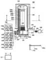
도 1은 본 개시의 각 형태에서 바람직하게 이용되는 기판 처리 장치의 종형 처리로의 개략 구성도이며, 처리로 부분을 종단면도로 도시하는 도면이다.
도 2는 본 개시의 각 형태에서 바람직하게 이용되는 기판 처리 장치의 종형 처리로의 개략 구성도이며, 처리로 부분을 도 1의 A-A선 단면도로 도시하는 도면이다.
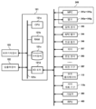
도 3은 본 개시의 각 형태에서 바람직하게 이용되는 기판 처리 장치의 컨트롤러의 개략 구성도이며, 컨트롤러의 제어계를 블록도로서 도시하는 도면이다.
도 4는 본 개시의 제1 형태에 있어서의 기판 처리 시퀀스를 도시하는 도면이다.
도 5는 본 개시의 제2 형태에 있어서의 기판 처리 시퀀스를 도시하는 도면이다.
도 6은 본 개시의 제3 형태에 있어서의 기판 처리 시퀀스를 도시하는 도면이다.
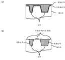
도 7은 실시예 및 비교예를 도시하는 도면이다.
도 8의 (a)는 실시예에 있어서의 웨이퍼 표면의 부분 단면 확대도이며, 도 8의 (b)는 비교예에 있어서의 웨이퍼 표면의 부분 단면 확대도이다.1 is a schematic configuration diagram of a vertical processing furnace of a substrate processing apparatus suitably used in each aspect of the present disclosure, and is a diagram showing a portion of the processing furnace in longitudinal section.
FIG. 2 is a schematic configuration diagram of a vertical processing furnace of a substrate processing apparatus suitably used in each aspect of the present disclosure, and is a diagram showing a portion of the processing furnace as a cross-sectional view taken along line AA in FIG. 1.
FIG. 3 is a schematic configuration diagram of a controller of a substrate processing apparatus suitably used in each aspect of the present disclosure, and is a block diagram showing the control system of the controller.
FIG. 4 is a diagram showing a substrate processing sequence in the first embodiment of the present disclosure.
FIG. 5 is a diagram showing a substrate processing sequence in the second embodiment of the present disclosure.
FIG. 6 is a diagram showing a substrate processing sequence in the third embodiment of the present disclosure.
Figure 7 is a diagram showing examples and comparative examples.
FIG. 8(a) is an enlarged view of a partial cross-section of the wafer surface in the example, and FIG. 8(b) is an enlarged view of a partial cross-section of the wafer surface in the comparative example.
<본 개시의 제1 형태><First form of present disclosure>
이하, 본 개시의 제1 형태에 대해서, 주로 도 1 내지 도 4를 참조하면서 설명한다. 또한 이하의 설명에 있어서 이용되는 도면은, 모두 모식적인 것이며, 도면에 도시되는 각 요소의 치수의 관계, 각 요소의 비율 등은, 현실의 것과 반드시 일치하지는 않는다. 또한 복수의 도면의 상호간에 있어서도, 각 요소의 치수의 관계, 각 요소의 비율 등은 반드시 일치하지는 않는다.Hereinafter, the first form of the present disclosure will be described mainly with reference to FIGS. 1 to 4. In addition, the drawings used in the following description are all schematic, and the dimensional relationships and ratios of each element shown in the drawings do not necessarily match those in reality. Moreover, even among a plurality of drawings, the relationship between the dimensions of each element and the ratio of each element do not necessarily match.
(1)기판 처리 장치의 구성(1) Configuration of substrate processing equipment
도 1에 도시하는 바와 같이, 처리로(202)는 가열 기구(온도 조정부)로서의 히터(207)를 포함한다. 히터(207)는 원통 형상이며, 보지판에 지지되는 것에 의해 수직으로 설치되어 있다. 히터(207)는, 가스를 열로 활성화(여기) 시키는 활성화 기구(여기부)로서도 기능한다.As shown in FIG. 1, the
히터(207)의 내측에는, 히터(207)와 동심원 형상으로 반응관(203)이 배설되어 있다. 반응관(203)은, 예컨대 석영(SiO2) 또는 탄화실리콘(SiC) 등의 내열성 재료에 의해 구성되고, 상단이 폐색하고 하단이 개구한 원통 형상으로 형성되어 있다. 반응관(203)의 하방에는, 반응관(203)과 동심원 형상으로 매니폴드(209)가 배설되어 있다. 매니폴드(209)는, 예컨대 스텐레스 강철(SUS) 등의 금속 재료에 의해 구성되고, 상단 및 하단이 개구한 원통 형상으로 형성되어 있다. 매니폴드(209)의 상단부는, 반응관(203)의 하단부에 계합되어 있고, 반응관(203)을 지지하도록 구성되어 있다. 매니폴드(209)와 반응관(203)과의 사이에는, 씰 부재로서의 O링(220a)이 설치되어 있다. 반응관(203)은 히터(207)와 마찬가지로 수직으로 설치되어 있다. 주로 반응관(203)과 매니폴드(209)에 의해 처리 용기(반응 용기)가 구성된다. 처리 용기의 통중공부에는 처리실(201)이 형성된다. 처리실(201)은, 기판으로서의 웨이퍼(200)를 수용 가능하도록 구성되어 있다. 이 처리실(201) 내에서 웨이퍼(200)에 대한 처리가 수행된다.Inside the
처리실(201) 내에는, 제1 내지 제3 공급부로서의 노즐(249a 내지 249c)이, 매니폴드(209)의 측벽을 관통하도록 각각 설치되어 있다. 노즐(249a 내지 249c)을 제1 내지 제3 노즐이라고도 부른다. 노즐(249a 내지 249c)은, 예컨대 석영 또는 SiC 등의 내열성 재료인 비금속 재료에 의해 구성되어 있다. 노즐(249a 내지 249c)에는, 가스 공급관(232a 내지 232c)이 각각 접속되어 있다. 노즐(249a 내지 249c)은 각각 다른 노즐이며, 노즐(249a, 249c)의 각각은, 노즐(249b)에 인접해서 설치되어 있다.Within the
가스 공급관(232a 내지 232c)에는, 가스의 흐름의 상류측에서 순서대로 유량 제어기(유량 제어부)인 매스 플로우 컨트롤러(MFC)(241a 내지 241c) 및 개폐 밸브인 밸브(243a 내지 243c)가 각각 설치되어 있다. 가스 공급관(232a)의 밸브(243a)보다도 하류측에는, 가스 공급관(232e)이 접속되어 있다. 가스 공급관(232b)의 밸브(243b)보다도 하류측에는, 가스 공급관(232d, 232f)이 각각 접속되어 있다. 가스 공급관(232c)의 밸브(243c)보다도 하류측에는, 가스 공급관(232g)이 접속되어 있다. 가스 공급관(232d 내지 232g)에는, 가스의 흐름의 상류측에서 순서대로 MFC(241d 내지 241g) 및 밸브(243d 내지 243g)가 각각 설치되어 있다. 가스 공급관(232a 내지 232g)은, 예컨대, SUS 등의 금속 재료에 의해 구성되어 있다.In the
도 2에 도시하는 바와 같이, 노즐(249a 내지 249c)은, 반응관(203)의 내벽과 웨이퍼(200)와의 사이에서의 평면시에 있어서 원환 형상의 공간에, 반응관(203)의 내벽의 하부로부터 상부를 따라, 웨이퍼(200)의 배열 방향 상방을 향해서 상승하도록 각각 설치되어 있다. 즉 노즐(249a 내지 249c)은, 웨이퍼(200)가 배열되는 웨이퍼 배열 영역의 측방의, 웨이퍼 배열 영역을 수평하게 둘러싸는 영역에, 웨이퍼 배열 영역에 따르도록 각각 설치되어 있다. 평면시에 있어서, 노즐(249b)은, 처리실(201) 내에 반입되는 웨이퍼(200)의 중심을 개재해서 후술하는 배기구(231a)와 일직선 상에 대향하게 배치되어 있다. 노즐(249a, 249c)은, 노즐(249b)과 배기구(231a)의 중심을 통하는 직선(L)을, 반응관(203)의 내벽(웨이퍼(200)의 외주부)에 따라 양측에서 끼워 넣게 배치되어 있다. 직선(L)은, 노즐(249b)과 웨이퍼(200)의 중심을 통하는 직선이기도 한다. 즉 노즐(249c)은, 직선(L)을 개재해서 노즐(249a)과 반대측에 설치되어 있다고 할 수도 있다. 노즐(249a, 249c)은, 직선(L)을 대칭축으로서 선대칭으로, 즉 시메트리로 배치되어 있다. 노즐(249a 내지 249c)의 측면에는, 가스를 공급하는 가스 공급공(250a 내지 250c)이 각각 설치되어 있다. 가스 공급공(250a 내지 250c)은, 각각이 평면시에 있어서 배기구(231a)와 상대(대면)하게 개구하고 있어, 웨이퍼(200)를 향해서 가스를 공급하는 것이 가능하도록 되어 있다. 가스 공급공(250a 내지 250c)은, 반응관(203)의 하부로부터 상부에 걸쳐서 복수 설치되어 있다.As shown in FIG. 2, the
가스 공급관(232a)으로부터는, 제1 반응물로서의 제1 원료 및 제2 반응물로서의 제2 원료가, MFC(241a), 밸브(243a), 노즐(249a)을 개재해서 처리실(201) 내에 공급된다.From the
가스 공급관(232b)으로부터는, 제1 반응물로서의 제1 반응체가, MFC(241b), 밸브(243b), 노즐(249b)을 개재해서 처리실(201) 내에 공급된다.From the
가스 공급관(232c)으로부터는, 제2 반응물로서의 제2 반응체가, MFC(241c), 밸브(243c), 노즐(249c)을 개재해서 처리실(201) 내에 공급된다.From the
가스 공급관(232d)으로부터는, 제2 반응물로서의 제3 반응체가, MFC(241d), 밸브(243d), 가스 공급관(232b), 노즐(249b)을 개재해서 처리실(201) 내에 공급된다.From the gas supply pipe 232d, the third reactant as the second reactant is supplied into the
가스 공급관(232e 내지 232g)으로부터는, 불활성 가스가, 각각 MFC(241e 내지 241g), 밸브(243e 내지 243g), 가스 공급관(232a 내지 232c), 노즐(249a 내지 249c)을 개재해서 처리실(201) 내에 공급된다. 불활성 가스는, 퍼지 가스, 캐리어 가스, 희석 가스 등으로서 작용한다.From the gas supply pipes 232e to 232g, the inert gas is supplied to the
주로 가스 공급관(232a, 232b), MFC(241a, 24lb), 밸브(243a, 243b)에 의해, 제1 반응물 공급계(제1 원료 공급계, 제1 반응체 공급계)가 구성된다. 주로 가스 공급관(232a, 232c, 232d), MFC(241a, 241c, 241d), 밸브(243a, 243c, 243d)에 의해, 제2 반응물 공급계(제2 원료 공급계, 제2 반응체 공급계, 제3 반응체 공급계)가 구성된다. 주로 가스 공급관(232e 내지 232g), MFC(241e 내지 241g), 밸브(243e 내지 243g)에 의해, 불활성 가스 공급계가 구성된다.The first reactant supply system (first raw material supply system, first reactant supply system) is mainly composed of
전술한 각종 공급계 가운데 어느 하나 또는 모든 공급계는, 밸브(243a 내지 243g)나 MFC(241a 내지 241g) 등이 집적되는 집적형 공급 시스템(248)으로서 구성되어 있어도 좋다. 집적형 공급 시스템(248)은, 가스 공급관(232a 내지 232g)의 각각에 대하여 접속되고, 가스 공급관(232a 내지 232g) 내로의 각종 가스의 공급 동작, 즉 밸브(243a 내지 243g)의 개폐 동작이나 MFC(241a 내지 241g)에 의한 유량 조정 동작 등이, 후술하는 컨트롤러(121)에 의해 제어되도록 구성되어 있다. 집적형 공급 시스템(248)은, 일체형 또는 분할형의 집적 유닛으로서 구성되어 있어, 가스 공급관(232a 내지 232g) 등에 대하여 집적 유닛 단위로 탈착을 수행할 수 있고, 집적형 공급 시스템(248)의 메인터넌스, 교환, 증설 등을 집적 유닛 단위로 수행하는 것이 가능하도록 구성되어 있다.Any or all of the various supply systems described above may be configured as an
반응관(203)의 측벽 하방으로는, 처리실(201) 내의 분위기를 배기하는 배기구(231a)가 설치되어 있다. 도 2에 도시하는 바와 같이, 배기구(231a)는, 평면시에 있어서, 웨이퍼(200)를 개재해서 노즐(249a 내지 249c)(가스 공급공(250a 내지 250c))과 상대(대면)하는 위치에 설치되어 있다. 배기구(231a)는, 반응관(203)의 측벽의 하부로부터 상부를 따라, 즉 웨이퍼 배열 영역에 따라 설치되어 있어도 좋다. 배기구(231a)에는 배기관(231)이 접속되어 있다. 배기관(231)은, 예컨대 SUS 등의 금속 재료에 의해 구성되어 있다. 배기관(231)에는, 처리실(201) 내의 압력을 검출하는 압력 검출기(압력 검출부)로서의 압력 센서(245) 및 압력 조정기(압력 조정부)로서의 APC(Auto Pressure Controller) 밸브(244)를 개재하여, 진공 배기 장치로서의 진공 펌프(246)가 접속되어 있다. APC 밸브(244)는, 진공 펌프(246)를 작동시킨 상태에서 밸브를 개폐하는 것에 의해, 처리실(201) 내의 진공 배기 및 진공 배기 정지를 수행할 수 있고, 또한 진공 펌프(246)를 작동시킨 상태에서, 압력 센서(245)에 의해 검출된 압력 정보에 기초해서 밸브 개도를 조절하는 것에 의해, 처리실(201) 내의 압력을 조정할 수 있도록 구성되어 있다. 주로 배기관(231), APC 밸브(244), 압력 센서(245)에 의해, 배기계가 구성된다. 진공 펌프(246)를 배기계에 포함시켜서 생각해도 좋다.An
매니폴드(209)의 하방에는, 매니폴드(209)의 하단 개구를 기밀하게 폐색 가능한 노구 개체(蓋體)로서의 씰 캡(219)이 설치되어 있다. 씰 캡(219)은, 예컨대 SUS 등의 금속 재료에 의해 구성되고, 원반 형상으로 형성되어 있다. 씰 캡(219)의 상면에는, 매니폴드(209)의 하단과 당접(當接)하는 씰 부재로서의 O링(220b)이 설치되어 있다. 씰 캡(219)의 하방에는, 후술하는 보트(217)를 회전시키는 회전 기구(267)가 설치된다. 회전 기구(267)의 회전축(255)은, 예컨대 SUS 등의 금속 재료에 의해 구성되고, 씰 캡(219)을 관통해서 보트(217)에 접속되어 있다. 회전 기구(267)는, 보트(217)를 회전시키는 것에 의해 웨이퍼(200)를 회전시키도록 구성되어 있다. 씰 캡(219)은, 반응관(203)의 외부에 설치된 승강 기구로서의 보트 엘리베이터(115)에 의해 수직 방향으로 승강되도록 구성되어 있다. 보트 엘리베이터(115)는, 씰 캡(219)을 승강시키는 것에 의해, 웨이퍼(200)를 처리실(201) 내외에 반입 및 반출(반송)하는 반송 장치(반송 기구)로서 구성되어 있다.A
매니폴드(209)의 하방에는, 씰 캡(219)을 강하시켜 보트(217)를 처리실(201) 내에서 반출한 상태에서, 매니폴드(209)의 하단 개구를 기밀하게 폐색 가능한 노구 개체로서의 셔터(219s)가 설치되어 있다. 셔터(219s)는, 예컨대 SUS 등의 금속 재료에 의해 구성되고, 원반 형상으로 형성되어 있다. 셔터(219s)의 상면에는, 매니폴드(209)의 하단과 당접하는 씰 부재로서의 O링(220c)이 설치되어 있다. 셔터(219s)의 개폐 동작(승강 동작이나 회동 동작 등)은, 셔터 개폐 기구(115s)에 의해 제어된다.Below the manifold 209, there is a shutter as a nozzle object that can airtightly block the lower end opening of the manifold 209 when the
기판 지지구로서의 보트(217)는, 복수 매, 예컨대 25 내지 200장의 웨이퍼(200)를, 수평 자세에서 또한, 서로 중심을 맞춘 상태에서 수직 방향으로 정렬시켜서 다단으로 지지하도록, 즉 간격을 두고서 배열시키도록 구성되어 있다. 보트(217)는, 예컨대 석영이나 SiC 등의 내열성 재료에 의해 구성된다. 보트(217)의 하부에는, 예컨대 석영이나 SiC 등의 내열성 재료에 의해 구성되는 단열판(218)이 다단으로 지지되어 있다.The
반응관(203) 내에는, 온도 검출기로서의 온도 센서(263)가 설치된다. 온도 센서(263)에 의해 검출된 온도 정보에 기초해 히터(207)에의 통전 상태를 조정하는 것에 의해, 처리실(201) 내의 온도가 원하는 온도 분포가 된다. 온도 센서(263)는, 반응관(203)의 내벽을 따라 설치되어 있다.Inside the
도 3에 도시하는 바와 같이, 제어부(제어 수단)인 컨트롤러(121)는, CPU(Central Processing Unit) 121a, RAM(Random Access Memory) 12lb, 기억 장치(121c), I/O 포트(121d)를 구비한 컴퓨터로서 구성되어 있다. RAM(121b), 기억 장치(121c), I/O 포트(121d)는, 내부 버스(121e)를 개재하고, CPU(121a)와 데이터 교환 가능하도록 구성되어 있다. 컨트롤러(121)에는, 예컨대 터치 패널 등으로서 구성된 입출력 장치(122)가 접속되어 있다. 또한 컨트롤러(121)에는, 외부 기억 장치(123)를 접속하는 것이 가능하도록 되어 있다.As shown in FIG. 3, the
기억 장치(121c)는, 예컨대 플래시 메모리, HDD(Hard Disk Drive), SSD(Solid State Drive) 등으로 구성되어 있다. 기억 장치(121c) 내에는, 기판 처리 장치의 동작을 제어하는 제어 프로그램이나 후술하는 기판 처리의 순서나 조건 등이 기재된 프로세스 레시피 등이, 판독 가능하도록 격납되어 있다. 프로세스 레시피는, 후술하는 기판 처리에 있어서의 각 순서를 컨트롤러(121)에 의해서 기판 처리 장치에 실행시켜, 소정의 결과를 얻을 수 있게 조합된 것이며, 프로그램으로서 기능한다. 이하, 프로세스 레시피나 제어 프로그램 등을 총칭하여 단순히 프로그램이라고도 말한다. 또한 프로세스 레시피를 단순히 레시피라고도 말한다. 본 명세서에 있어서 프로그램이라고 하는 용어를 이용하는 경우는, 레시피 단체(單體)만을 포함하는 경우, 제어 프로그램 단체만을 포함하는 경우 또는 그들의 양방을 포함하는 경우가 있다. RAM(121b)은, CPU(121a)에 의해 판독된 프로그램이나 데이터 등이 일시적으로 보지되는 메모리 영역(work area)으로서 구성되어 있다.The
I/O 포트(121d)는, 전술한 MFC(241a 내지 241g), 밸브(243a 내지 243g), 압력 센서(245), APC 밸브(244), 진공 펌프(246), 온도 센서(263), 히터(207), 회전 기구(267), 보트 엘리베이터(115), 셔터 개폐 기구(115s) 등에 접속되어 있다.The I/
CPU(121a)는, 기억 장치(121c)로부터 제어 프로그램을 판독해서 실행하는 것과 함께, 입출력 장치(122)로부터의 조작 커맨드의 입력 등에 따라서 기억 장치(121c)로부터 레시피를 판독하는 것이 가능하도록 구성되어 있다. CPU(121a)는, 판독한 레시피의 내용을 따르도록, MFC(241a 내지 241g)에 의한 각종 가스의 유량 조정 동작, 밸브(243a 내지 243g)의 개폐 동작, APC 밸브(244)의 개폐 동작 및 압력 센서(245)에 기초하는 APC 밸브(244)에 의한 압력 조정 동작, 진공 펌프(246)의 기동 및 정지, 온도 센서(263)에 기초하는 히터(207)의 온도 조정 동작, 회전 기구(267)에 의한 보트(217)의 회전 및 회전 속도 조절 동작, 보트 엘리베이터(115)에 의한 보트(217)의 승강 동작, 셔터 개폐 기구(115s)에 의한 셔터(219s)의 개폐 동작 등을 제어하는 것이 가능하도록 구성되어 있다.The
컨트롤러(121)는, 외부 기억 장치(123)에 격납된 전술한 프로그램을 컴퓨터에 인스톨하는 것에 의해 구성할 수 있다. 외부 기억 장치(123)는, 예컨대 HDD 등의 자기 디스크, CD 등의 광 디스크, MO 등의 광자기 디스크, USB 메모리, SSD 등의 반도체 메모리 등을 포함한다. 기억 장치(121c)나 외부 기억 장치(123)는, 컴퓨터 판독 가능한 기록 매체로서 구성되어 있다. 이하, 이들을 총칭하여 단순히 기록 매체라고도 한다. 본 명세서에 있어서 기록 매체라고 하는 용어를 이용하는 경우는, 기억 장치(121c) 단체만을 포함하는 경우, 외부 기억 장치(123) 단체만을 포함하는 경우 또는 그들의 양방을 포함하는 경우가 있다. 또한 컴퓨터로의 프로그램의 제공은, 외부 기억 장치(123)를 이용하지 않고, 인터넷이나 전용 회선 등의 통신 수단을 이용해서 수행해도 좋다.The
(2) 기판 처리 공정(2) Substrate processing process
전술한 기판 처리 장치를 이용하여, 반도체 장치의 제조 공정의 일 공정으로서 기판으로서의 웨이퍼(200)의 표면 상에 막을 형성하는 처리 시퀀스예에 대해서, 주로 도 4를 이용해서 설명한다. 또한 본 형태에서는, 웨이퍼(200)로서, 그 표면에 트렌치나 홀 등의 요부가 설치되고, 실리콘(Si) 및 산소(O) 함유막 등의 O 함유막이 노출된 실리콘 기판(실리콘 웨이퍼)을 이용하는 예에 대해서 설명한다. 또한 웨이퍼(200)의 표면에 노출되는 O 함유막은 자연 산화막이여도 좋다. 이하의 설명에 있어서, 기판 처리 장치를 구성하는 각 부의 동작은 컨트롤러(121)에 의해 제어된다.An example of a processing sequence for forming a film on the surface of a
도 4에 도시하는 바와 같이, 본 형태의 처리 시퀀스에서는, 표면에 요부가 설치되고 O 함유막이 노출된 웨이퍼(200)에 대하여 제1 온도 하에서 제1 반응물(제1 원료, 제1 반응체)을 공급하는 것에 의해, 웨이퍼(200)의 표면 상에 유동성이 없는 막(이하, "비유동성 막"이라고도 부른다)을 형성하는 스텝A(비유동성 막 형성)와 (b) 웨이퍼(200)에 대하여 제1 온도보다도 낮은 제2 온도 하에서 제2 반응물(제2 원료, 제2 반응체, 제3 반응체)을 공급하는 것에 의해, 비유동성 막 상에 유동성 막을 형성하는 스텝B(유동성 막 형성)를 수행한다.As shown in FIG. 4, in the processing sequence of this form, the first reactant (first raw material, first reactant) is applied to the
또한 도 4에서는, 제1 원료와 제2 원료가 동일한 원료이며, 제1 반응체와 제3 반응체가 동일한 반응체인 예를 제시하고 있다. 즉 도 4에서는, 제1 원료와 제2 원료의 분자 구조가 동일하고, 제1 반응체와 제3 반응체의 분자 구조가 동일한 예를 제시하고 있다. 이러한 점은, 후술하는 제2 형태, 제3 형태에서의 도 5, 도 6에서도 마찬가지이다.In addition, FIG. 4 shows an example where the first raw material and the second raw material are the same raw material, and the first reactant and the third reactant are the same reactant. That is, Figure 4 presents an example in which the molecular structures of the first and second raw materials are the same, and the molecular structures of the first reactant and the third reactant are the same. This also applies to FIGS. 5 and 6 in the second and third forms described later.
또한 본 형태의 처리 시퀀스에서는, 비유동성 막 상에 유동성 막이 형성된 후의 웨이퍼(200)에 대하여 제2 온도보다도 높은 제3 온도 하에서 포스트 트리트먼트를 수행하는 것에 의해, 유동성 막을 개질시키는 스텝C(포스트 트리트먼트)을 더 수행한다. 본 명세서에서는, 포스트 트리트먼트를 "PT"라고도 칭한다.In addition, in the processing sequence of this form, post-treatment is performed on the
또한 본 형태의 처리 시퀀스에서는, 전술한 스텝A에 있어서, 웨이퍼(200)에 대하여 제1 원료를 공급하는 스텝A1 및 웨이퍼(200)에 대하여 제1 반응체를 공급하는 스텝A2를 포함하는 사이클을 소정 횟수(m회, m은 1이상의 정수) 수행한다. 본 형태의 처리 시퀀스에서는, 스텝A1, A2를 비동시로 수행한다.In addition, in the processing sequence of this form, in the above-described step A, a cycle including step A1 for supplying the first raw material to the
또한 본 형태의 처리 시퀀스에서는, 전술한 스텝B에 있어서, 웨이퍼(200)에 대하여 제2 원료를 공급하는 스텝B1과 웨이퍼(200)에 대하여 제2 반응체를 공급하는 스텝B2와 웨이퍼(200)에 대하여 제3 반응체를 공급하는 스텝B3를 포함하는 사이클을 소정 횟수(n회, n은 1이상의 정수) 수행한다. 본 형태의 처리 시퀀스에서는, 스텝B1, B2, B3을 비동시로 수행한다.In addition, in the processing sequence of this form, in the above-described Step B, Step B1 for supplying the second raw material to the
본 명세서에서는, 전술한 처리 시퀀스를, 편의상, 아래와 같이 도시할 수도 있다. 이하의 제2, 제3 형태 등을 포함하는 변형예 등의 설명에 있어서도, 같은 표기를 이용한다.In this specification, the above-described processing sequence may be shown as follows for convenience. The same notation is used in the description of modifications including the second and third forms below.
(제1 원료→제1 반응체)×m→(제2 원료→제2 반응체→제3 반응체)×n→PT(first raw material → first reactant) × m → (second raw material → second reactant → third reactant) × n → PT
본 명세서에 있어서 「웨이퍼」라고 하는 용어를 이용하는 경우는, 웨이퍼 그 자체를 의미하는 경우나, 웨이퍼와 그 표면에 형성된 소정의 층이나 막과의 적층체를 의미하는 경우가 있다. 본 명세서에 있어서 「웨이퍼의 표면」이라고 하는 용어를 이용하는 경우는, 웨이퍼 그 자체의 표면을 의미하는 경우나, 웨이퍼 상에 형성된 소정의 층 등의 표면을 의미하는 경우가 있다. 본 명세서에 있어서 「웨이퍼 상에 소정의 층을 형성한다」라고 기재했을 경우는, 웨이퍼 그 자체의 표면 상에 소정의 층을 직접 형성하는 것을 의미하는 경우나, 웨이퍼 상에 형성되어 있는 층 등 위에 소정의 층을 형성하는 것을 의미하는 경우가 있다. 본 명세서에 있어서 「기판」이라고 하는 용어를 이용하는 경우도, 「웨이퍼」라는 용어를 이용하는 경우와 같은 의미이다.When the term “wafer” is used in this specification, it may mean the wafer itself or a laminate of a wafer and a predetermined layer or film formed on the surface. In this specification, when the term “wafer surface” is used, it may mean the surface of the wafer itself or the surface of a predetermined layer formed on the wafer. In this specification, when it is described as “forming a predetermined layer on the wafer,” it means forming a predetermined layer directly on the surface of the wafer itself, or on a layer formed on the wafer, etc. In some cases, it means forming a predetermined layer. In this specification, the use of the term “substrate” has the same meaning as the use of the term “wafer.”
(웨이퍼 차지 및 보트 로드)(wafer charge and boat load)
복수 매의 웨이퍼(200)가 보트(217)에 장전(웨이퍼 차지)된 후, 셔터 개폐 기구(115s)에 의해 셔터(219s)를 이동시켜, 매니폴드(209)의 하단 개구가 개방된다(셔터 오픈). 그 후, 도 1에 도시하는 바와 같이, 복수 매의 웨이퍼(200)를 지지한 보트(217)는, 보트 엘리베이터(115)에 의해 들어 올려져서 처리실(201) 내에 반입(보트 로드)된다. 이 상태에서 씰 캡(219)은, O링(220b)을 개재해서 매니폴드(209)의 하단을 밀봉한 상태가 된다.After a plurality of
(압력 조정 및 온도 조정)(pressure adjustment and temperature adjustment)
보트 로드가 종료한 후, 처리실(201) 내, 즉 웨이퍼(200)가 존재하는 공간이 원하는 압력(진공도)이 되도록, 진공 펌프(246)에 의해 진공 배기(감압 배기)된다. 이 때 처리실(201) 내의 압력은 압력 센서(245)에서 측정되고, 이 측정된 압력 정보에 기초해 APC 밸브(244)가 피드백 제어된다(압력 조정). 또한 처리실(201) 내의 웨이퍼(200)가 원하는 처리 온도가 되도록, 히터(207)에 의해 가열된다. 이 때 처리실(201) 내가 원하는 온도 분포가 되도록, 온도 센서(263)가 검출한 온도 정보에 기초하여 히터(207)로의 통전 상태가 피드백 제어된다(온도 조정). 또한 회전 기구(267)에 의한 웨이퍼(200)의 회전을 시작한다. 처리실(201) 내의 배기, 웨이퍼(200)의 가열 및 회전은, 모두 적어도 웨이퍼(200)에 대한 처리가 종료할 때까지의 동안에는 계속해서 수행된다.After boat loading is completed, the inside of the
(성막 처리)(Tabernacle processing)
그 후, 스텝A 내지 C를 이 순서대로 실행하여, 웨이퍼(200) 상에의 성막 처리를 수행한다. 본 명세서에서는, 웨이퍼(200)의 표면에 설치된 요부 내로의 성막 처리를, 매립 처리라고도 부른다. 이하, 이들의 각 스텝에 대해서 설명한다.Thereafter, steps A to C are executed in this order to perform a film forming process on the
[스텝A(비유동성 막 형성)][Step A (formation of non-fluidic film)]
스텝A에서는, 처리실(201) 내의 웨이퍼(200), 즉 표면에 요부가 설치되고 O 함유막이 노출된 웨이퍼(200)에 대하여, 제1 반응물(제1 원료, 제1 반응체)을 공급하는 것에 의해, 웨이퍼(200)의 표면 상에 비유동성 막을 형성한다. 스텝A에서는, 제1 원료가 단독으로 존재했을 경우에 제1 원료의 물리 흡착보다도 제1 원료의 화학 흡착 또는 열 분해가 지배적으로 발생하는 조건 하에서, 제1 원료와 제1 반응체를 공급한다.In step A, the first reactant (first raw material, first reactant) is supplied to the
구체적으로는, 스텝A에서는, 웨이퍼(200)에 대하여 제1 원료를 공급하는 스텝A1과 웨이퍼(200)에 대하여 제1 반응체를 공급하는 스텝A2를 포함하는 사이클을 소정 횟수(m회, m은 1이상의 정수) 수행한다. 이하, 스텝A1, A2를 포함하는 스텝A에 대해서 보다 구체적으로 설명한다.Specifically, in Step A, a cycle including Step A1 for supplying the first raw material to the
[스텝A1][Step A1]
스텝A1에서는, 처리실(201) 내의 웨이퍼(200)에 대하여 제1 원료를 공급한다.In step A1, the first raw material is supplied to the
구체적으로는, 밸브(243a)를 열고, 가스 공급관(232a) 내에 제1 원료를 흘린다. 제1 원료는, MFC(241a)에 의해 유량 조정되고, 노즐(249a)을 개재해서 처리실(201) 내에 공급되고, 배기구(231a)를 통하여 배기된다. 이 때 웨이퍼(200)에 대하여 제1 원료가 공급된다(제1 원료 공급). 이 때 밸브(243e 내지 243g)를 열고, 노즐(249a 내지 249c)의 각각을 개재해서 처리실(201) 내에 불활성 가스를 공급해도 좋다.Specifically, the
소정의 시간이 경과한 후, 밸브(243a)를 닫고, 처리실(201) 내로의 제1 원료의 공급을 정지한다. 그리고 처리실(201) 내를 진공 배기하여, 처리실(201) 내에 잔류하는 가스 상(狀) 물질 등을 처리실(201) 내에서 배제한다. 이 때 밸브(243e 내지 243g)를 열고, 노즐(249a 내지 249c)을 개재해서 처리실(201) 내에 불활성 가스를 공급한다. 노즐(249a 내지 249c)을 통하여 공급되는 불활성 가스는 퍼지 가스로서 작용하고, 이에 의해 웨이퍼(200)가 존재하는 공간, 즉 처리실(201) 내가 퍼지된다(퍼지).After a predetermined time has elapsed, the
제1 원료로서는, 예컨대 웨이퍼(200)의 표면 상에 형성되는 비유동성 막을 구성하는 주 원소로서의 실리콘(Si)을 포함하는 실란계 가스를 이용할 수 있다. 실란계 가스로서는, 예컨대 Si 및 할로겐을 함유하는 가스, 즉 할로실란계 가스를 이용할 수 있다. 할로겐에는, 염소(Cl), 불소(F), 브롬(Br), 요오드(I) 등이 포함된다. 즉 할로실란계 가스는, 클로로실란계 가스, 플루오로실란계 가스, 브로모실란계 가스, 요오드실란계 가스 등을 포함한다. 할로실란계 가스로서는, 예컨대 실리콘, 탄소(C) 및 할로겐을 함유하는 가스, 즉 유기 할로실란계 가스를 이용할 수 있다. 유기 할로실란계 가스로서는, 예컨대 Si, C 및 Cl을 포함하는 가스, 즉 유기 클로로실란계 가스를 이용할 수 있다.As the first raw material, for example, a silane-based gas containing silicon (Si) as the main element constituting the non-flowing film formed on the surface of the
제1 원료로서는, 예컨대 모노실란(SiH4, 약칭:MS) 가스, 디실란(Si2H6, 약칭:DS) 가스 등의 C 및 할로겐 비함유의 실란계 가스나, 디클로로실란(SiH2Cl2, 약칭:DCS) 가스, 헥사클로로디실란(Si2Cl6, 약칭:HCDS) 가스 등의 C비함유의 할로실란계 가스나, 트리메틸실란(SiH(CH3)3, 약칭:TMS) 가스, 디메틸실란(SiH2(CH3)2, 약칭:DMS) 가스, 트리에틸실란(SiH(C2H5)3, 약칭:TES) 가스, 디에틸실란(SiH2(C2H5)2, 약칭:DES) 가스 등의 알킬실란계 가스나, 비스(트리클로로실릴)메탄((SiCl3)2CH2,, 약칭:BTCSM) 가스, 1, 2-비스(트리클로로실릴)에탄((SiCl3)2C2H4, 약칭:BTCSE) 가스 등의 알킬렌할로실란계 가스나, 트리메틸클로로실란(SiCl(CH3)3, 약칭:TMCS) 가스, 디메틸디클로로실란(SiCl2(CH3)2, 약칭:DMDCS) 가스, 트리에틸클로로실란(SiCl(C2H5)3, 약칭:TECS) 가스, 디에틸디클로로실란(SiCl2(C2H5)2, 약칭:DEDCS) 가스, 1, 1, 2, 2-테트라클로로-1, 2- 디메틸디실란((CH3)2Si2Cl4, 약칭:TCDMDS) 가스, 1, 2-디클로로-1, 1, 2, 2-테트라메틸디실란((CH3)4Si2Cl2, 약칭:DCTMDS) 가스 등의 알킬할로실란계 가스를 이용할 수 있다. 또한 제1 원료로서는, 예컨대 (디메틸아미노)트리메틸실란((CH3)2NSi(CH3)3, 약칭:DMATMS) 가스, (디에틸아미노)트리에틸실란)(C2H5)2NSi(C2H5)3, 약칭:DEATES) 가스, (디메틸아미노)트리에틸실란((CH3)2NSi(C2H5)3, 약칭:DMATES) 가스, (디에틸아미노)트리메틸실란((C2H5)2NSi(CH3)3, 약칭:DEATMS) 가스, (트리메틸실릴)아민((CH3)3SiNH2, 약칭:TMSA) 가스, (트리에틸실릴)아민((C2H5)3SiNH2, 약칭:TESA), (디메틸아미노)실란((CH3)2NSiH3, 약칭:DMAS) 가스, (디에틸아미노)실란((C2H5)2NSiH3, 약칭:DEAS) 가스 등의 알킬아미노실란계 가스를 이용할 수 있다. 제1 원료로서는, 이들의 실리콘 함유 원료 가운데 1 이상을 이용할 수 있다.As the first raw material, for example, C and halogen-free silane-based gas such as monosilane (SiH 4 , abbreviated name: MS) gas, disilane (Si 2 H 6 , abbreviated name: DS) gas, or dichlorosilane (SiH 2 Cl 2 , abbreviated name: DCS) gas, C-free halosilane-based gas such as hexachlorodisilane (Si 2 Cl 6 , abbreviated name: HCDS) gas, and trimethylsilane (SiH(CH 3 ) 3 , abbreviated name: TMS) gas. , dimethylsilane (SiH 2 (CH 3 ) 2 , abbreviated name: DMS) gas, triethylsilane (SiH (C 2 H 5 ) 3 , abbreviated name: TES) gas, diethylsilane (SiH 2 (C 2 H 5 ) 2 , abbreviated name: DES) gas, alkylsilane-based gases such as bis (trichlorosilyl) methane ((SiCl 3 ) 2 CH 2 ,, abbreviated name: BTCSM) gas, 1, 2-bis (trichlorosilyl) ethane (( Alkylene halosilane-based gas such as SiCl 3 ) 2 C 2 H 4 , abbreviated name: BTCSE) gas, trimethylchlorosilane (SiCl(CH 3 ) 3 , abbreviated name: TMCS) gas, and dimethyldichlorosilane (SiCl 2 (CH) 3 ) 2 , abbreviated name: DMDCS) gas, triethylchlorosilane (SiCl(C 2 H 5 ) 3 , abbreviated name: TECS) gas, diethyldichlorosilane (SiCl 2 (C 2 H 5 ) 2 , abbreviated name: DEDCS) gas , 1, 1, 2, 2-tetrachloro-1, 2- dimethyldisilane ((CH 3 ) 2 Si 2 Cl 4 , abbreviated name: TCDMDS) gas, 1, 2-dichloro-1, 1, 2, 2- Alkylhalosilane-based gases such as tetramethyldisilane ((CH 3 ) 4 Si 2 Cl 2 , abbreviated name: DCTMDS) gas can be used. Also, as the first raw material, for example, (dimethylamino)trimethylsilane ((CH 3 ) 2 NSi(CH 3 ) 3 , abbreviated name: DMATMS) gas, (diethylamino)triethylsilane) (C 2 H 5 ) 2 NSi ( C 2 H 5 ) 3 , abbreviated name: DEATES) gas, (dimethylamino)triethylsilane ((CH 3 ) 2 NSi(C 2 H 5 ) 3 , abbreviated name: DMATES) gas, (diethylamino)trimethylsilane (( C 2 H 5 ) 2 NSi(CH 3 ) 3 , abbreviated name: DEATMS) gas, (trimethylsilyl)amine ((CH 3 ) 3 SiNH 2 , abbreviated name: TMSA) gas, (triethylsilyl)amine ((C 2 H 5 ) 3 SiNH 2 , abbreviated name: TESA), (dimethylamino)silane ((CH 3 ) 2 NSiH 3 , abbreviated name: DMAS) gas, (diethylamino)silane ((C 2 H 5 ) 2 NSiH 3 , abbreviated name: Alkylaminosilane-based gases such as DEAS) gas can be used. As the first raw material, one or more of these silicon-containing raw materials can be used.
또한 이들의 제1 원료의 일부는 아미노기 비함유이며 할로겐을 함유한다. 또한 이들의 제1 원료의 일부는 실리콘과 실리콘의 화학 결합(Si-Si결합)을 함유한다. 또한 이들의 제1 원료의 일부는 실리콘 및 할로겐을 함유하거나 또는 실리콘, 할로겐 및 탄소를 함유한다. 또한 이들의 제1 원료의 일부는 알킬기와 할로겐을 함유한다.Additionally, some of these first raw materials do not contain amino groups and contain halogen. Additionally, some of these first raw materials contain silicon and a chemical bond of silicon (Si-Si bond). Additionally, some of these first raw materials contain silicon and halogen or contain silicon, halogen, and carbon. Additionally, some of these first raw materials contain alkyl groups and halogens.
불활성 가스로서는, 질소(N2) 가스나, 아르곤(Ar) 가스, 헬륨(He) 가스, 네온(Ne) 가스, 크세논(Xe) 가스 등의 희가스를 이용할 수 있다. 이 점은, 후술하는 각 스텝에 있어서도 마찬가지이다. 불활성 가스로서는, 이들 가운데 1 이상을 이용할 수 있다.As the inert gas, rare gases such as nitrogen (N 2 ) gas, argon (Ar) gas, helium (He) gas, neon (Ne) gas, or xenon (Xe) gas can be used. This also applies to each step described later. As the inert gas, one or more of these can be used.
[스텝A2][Step A2]
스텝A2에서는, 처리실(201) 내의 웨이퍼(200)에 대하여 제1 반응체를 공급한다.In step A2, the first reactant is supplied to the
구체적으로는, 밸브(243b)를 열고, 가스 공급관(232b) 내에 제1 반응체를 흘린다. 제1 반응체는, MFC(241b)에 의해 유량 조정되고, 노즐(249b)을 개재해서 처리실(201) 내에 공급되고, 배기구(231a)를 통하여 배기된다. 이 때 웨이퍼(200)에 대하여 제1 반응체가 공급된다(제1 반응체 공급). 이 때 밸브(243e 내지 243g)를 열고, 노즐(249a 내지 249c)의 각각을 개재해서 처리실(201) 내에 불활성 가스를 공급하도록 해도 좋다.Specifically, the
소정의 시간이 경과한 후, 밸브(243b)를 닫고, 처리실(201) 내로의 제1 반응체의 공급을 정지한다. 그리고 스텝A1에서의 퍼지와 같은 처리 순서에 의해, 처리실(201) 내에 잔류하는 가스 상 물질 등을 처리실(201) 내에서 배제한다.After a predetermined time has elapsed, the
제1 반응체로서는, 예컨대 질소(N) 및 수소(H) 함유 가스를 이용할 수 있다. N 및 H 함유 가스로서는, 예컨대 암모니아(NH3) 가스 등의 질화수소계 가스나, 모노에틸아민(C2H5NH2, 약칭:MEA) 가스, 디에틸아민((C2H5)2NH, 약칭:DEA) 가스, 트리에틸아민((C2H5)3N, 약칭:TEA) 가스 등의 에틸아민계 가스나, 모노메틸아민(CH3NH2, 약칭: MMA) 가스, 디메틸아민((CH3)2NH, 약칭: DMA) 가스, 트리메틸아민((CH3)3N, 약칭: TMA) 가스 등의 메틸아민계 가스나, 피리딘(C5H5N) 가스, 피페라진(C4H10N2) 가스 등의 환 형상 아민계 가스나, 모노메틸히드라진((CH3)HN2H2, 약칭:MMH) 가스, 디메틸히드라진((CH3)2N2H2, 약칭:DMH) 가스, 트리메틸히드라진((CH3)2N2(CH3)H, 약칭:TMH) 가스 등의 유기 히드라진계 가스를 이용할 수 있다. 또한 아민계 가스나 유기 히드라진계 가스는, C, N 및 H에 의해 구성되는 것이므로, 이들의 가스를 C, N 및 H 함유 가스라고 부를 수도 있다. 전술한 알킬기를 포함하는 아민계 가스를 알킬 아민계 가스라고 부를 수도 있다. C, N 및 H 함유 가스의 대신에, 에틸렌(C2H4) 가스, 아세틸렌(C2H2) 가스, 프로필렌(C3H6) 등의 C 함유 가스(C 및 H 함유 가스) 및 NH3가스 등의 N함유 가스(N 및 H 함유 가스)를 동시 또는 비동시에 공급하도록 해도 좋다. 제1 반응체로서는, 이들의 N 및 H 함유 반응체 또는 C, N 및 H 함유 반응체 가운데 1 이상을 이용할 수 있다.As the first reactant, for example, nitrogen (N) and hydrogen (H)-containing gas can be used. Examples of the N- and H-containing gas include hydrogen nitride-based gas such as ammonia (NH 3 ) gas, monoethylamine (C 2 H 5 NH 2 , abbreviated name: MEA) gas, and diethylamine ((C 2 H 5 ) 2 NH, abbreviated name: DEA) gas, ethylamine-based gas such as triethylamine ((C 2 H 5 ) 3 N, abbreviated name: TEA) gas, monomethylamine (CH 3 NH 2 , abbreviated name: MMA) gas, dimethyl Methylamine-based gases such as amine ((CH 3 ) 2 NH, abbreviated name: DMA) gas, trimethylamine ((CH 3 ) 3 N, abbreviated name: TMA) gas, pyridine (C 5 H 5 N) gas, and piperazine Ring-shaped amine-based gas such as (C 4 H 10 N 2 ) gas, monomethylhydrazine ((CH 3 )HN 2 H 2 , abbreviated name: MMH) gas, dimethylhydrazine ((CH 3 ) 2 N 2 H 2 , Organic hydrazine-based gases such as (abbreviated name: DMH) gas and trimethylhydrazine ((CH 3 ) 2 N 2 (CH 3 )H (abbreviated name: TMH) gas can be used. Additionally, since amine-based gas and organic hydrazine-based gas are composed of C, N, and H, these gases may also be called C, N, and H-containing gases. The amine-based gas containing the above-described alkyl group may also be called an alkyl amine-based gas. Instead of C, N and H containing gases, C containing gases (C and H containing gases) such as ethylene (C 2 H 4 ) gas, acetylene (C 2 H 2 ) gas, propylene (C 3 H 6 ) and NH N-containing gas (N- and H-containing gas) such as 3 gas may be supplied simultaneously or non-simultaneously. As the first reactant, one or more of these N- and H-containing reactants or C, N, and H-containing reactants can be used.
[소정 횟수 실시][Perform a certain number of times]
전술한 스텝A1 및 스텝A2을 비 동시에 즉 동기시키지 않고 수행하는 사이클을 소정 횟수(m회, m은 1이상의 정수) 수행한다. 이 때 제1 원료가 단독으로 존재했을 경우에 제1 원료의 물리 흡착보다도 제1 원료의 화학 흡착 또는 열 분해가 지배적으로 발생하는 조건 하에서, 전술한 사이클을 소정 횟수 수행한다.The cycle of performing the above-described step A1 and step A2 asynchronously, that is, without synchronization, is performed a predetermined number of times (m times, where m is an integer of 1 or more). At this time, when the first raw material exists alone, the above-described cycle is performed a predetermined number of times under conditions in which chemical adsorption or thermal decomposition of the first raw material occurs more dominantly than physical adsorption of the first raw material.
스텝A1에 있어서 제1 원료를 공급할 때의 처리 조건으로서는, 처리 온도(제1 온도): 350 ℃ 내지 700 ℃, 보다 바람직하게는 450 ℃ 내지 650 ℃, 처리 압력: 1 Pa 내지 2666 Pa, 바람직하게는 67 Pa 내지 1333 Pa, 제1 원료 공급 유량: 0.001 slm 내지 2 slm, 바람직하게는 0.01 slm 내지 1 slm, 제1 원료 공급 시간: 1초 내지 120초, 바람직하게는 1초 내지 60초, 불활성 가스 공급 유량(가스 공급관마다): 0 slm 내지 20 slm, 바람직하게는 0.01 slm 내지 10 slm이 예시된다.Processing conditions for supplying the first raw material in step A1 include: processing temperature (first temperature): 350°C to 700°C, more preferably 450°C to 650°C, and processing pressure: 1 Pa to 2666 Pa, preferably is 67 Pa to 1333 Pa, first raw material supply flow rate: 0.001 slm to 2 slm, preferably 0.01 slm to 1 slm, first raw material supply time: 1 second to 120 seconds, preferably 1 second to 60 seconds, inert Gas supply flow rate (per gas supply pipe): 0 slm to 20 slm, preferably 0.01 slm to 10 slm.
본 명세서에서 「350 ℃ 내지 700 ℃」와 같은 수치 범위의 표기는, 하한값 및 상한치가 그 범위에 포함되는 것을 의미한다. 따라서 예컨대 「350 ℃ 내지 700 ℃」는 「350 ℃ 이상 700 ℃ 이하」를 의미한다. 다른 수치 범위에 대해서도 마찬가지이다. 또한 본 명세서에서 처리 온도는 웨이퍼(200)의 온도 또는 처리실(201) 내의 온도를 의미하고, 처리 압력은 처리실(201) 내의 압력을 의미한다. 또한 가스 공급 유량이 0 slm이라는 것은, 그 가스를 공급하지 않는 케이스를 의미한다. 이러한 점들은, 이하의 설명에 있어서도 마찬가지이다.In this specification, the expression of a numerical range such as “350°C to 700°C” means that the lower limit and upper limit are included in the range. Therefore, for example, “350°C to 700°C” means “350°C or more and 700°C or less.” The same goes for other numerical ranges. Additionally, in this specification, processing temperature refers to the temperature of the
스텝A2에 있어서 제1 반응체를 공급할 때의 처리 조건으로서는, 처리 압력: 1 Pa 내지 4000 Pa, 바람직하게는 1 Pa 내지 3000 Pa, 제1 반응체 공급 유량: 0.001 slm 내지 20 slm, 바람직하게는 1 slm 내지 10 slm, 제1 반응체 공급 시간: 1초 내지 120초, 바람직하게는 1초 내지 60초가 예시된다. 다른 처리 조건은, 제1 원료를 공급할 때의 처리 조건과 동일하게 할 수 있다.The processing conditions when supplying the first reactant in step A2 include: processing pressure: 1 Pa to 4000 Pa, preferably 1 Pa to 3000 Pa, first reactant supply flow rate: 0.001 slm to 20 slm, preferably Examples include 1 slm to 10 slm, first reactant supply time: 1 second to 120 seconds, preferably 1 second to 60 seconds. Other processing conditions can be the same as those used when supplying the first raw material.
전술한 처리 조건 하에서 스텝A1에서 제1 원료를 공급하는 것에 의해, 스텝A1에서는, 제1 원료의 분자의 분자 구조의 일부를, 웨이퍼(200)의 표면과 요부 내의 표면, 즉 O 함유막의 표면에 흡착시킬 수 있다. 또한 전술한 처리 조건 하에서 스텝A2에서 제1 반응체를 공급하는 것에 의해, 스텝A2에서는, O 함유막의 표면에 흡착시킨 제1 원료의 분자의 분자 구조의 일부를 제1 반응체와 반응시켜서 비유동성 층을 형성할 수 있다. 비유동성 층은, 웨이퍼(200)의 표면과 요부 내의 표면에 컨포멀(conformal)하게 형성되고, 높은 스텝 커버리지를 가지는 층이 된다. 그리고 전술한 처리 조건 하에서 전술한 사이클을 소정 횟수 수행하는 것에 의해, 웨이퍼(200)의 표면과 요부 내의 표면, 즉 O 함유막의 표면에 소정 두께의 비유동성 막이 형성된다.By supplying the first raw material in step A1 under the above-described processing conditions, in step A1, a part of the molecular structure of the molecules of the first raw material is transferred to the surface of the
전술한 사이클은, 복수 회 반복하는 것이 바람직하다. 즉 1사이클당 형성되는 비유동성 층의 두께를 원하는 두께보다도 얇게 하고, 비유동성 층을 적층하는 것에 의해 형성되는 비유동성 막의 두께가 원하는 두께가 될때까지, 전술한 사이클을 복수 회 반복하는 것이 바람직하다. 또한 비유동성 막의 두께는, 후술하는 유동성 막의 두께 이하로 하거나 또는 후술하는 유동성 막의 두께보다도 얇게 하는 것이 바람직하다. 비유동성 막의 두께는, 예컨대 0.2nm 이상 10nm 이하로 하는 것이 바람직하다.The above-described cycle is preferably repeated multiple times. That is, it is preferable to make the thickness of the non-flowable layer formed per cycle thinner than the desired thickness and repeat the above-mentioned cycle multiple times until the thickness of the non-flowable film formed by laminating the non-flowable layer reaches the desired thickness. . In addition, it is preferable that the thickness of the non-flowable film is less than or equal to the thickness of the flowable film described later, or is thinner than the thickness of the fluidized film described later. The thickness of the non-flowable film is preferably, for example, 0.2 nm or more and 10 nm or less.
전술에서 예시한 각종 제1 원료, 각종 제1 반응체를 이용하는 경우, 비유동성 막으로서 예컨대 실리콘 질화막(SiN막) 등의 Si 및 N 함유막이나, 실리콘 탄질화막(SiCN막) 등의 Si, C 및 N 함유막을 형성할 수 있다. 전술한 각종 제1 원료, 각종 제1 반응체는 모두 O 비함유이므로, 비유동성 막은 O 비함유막이 된다. 또한 비유동성 막은, 성막의 하지가 되는 O 함유막보다도 친수성이 낮은 막이 된다. 성막의 하지가 되는 O 함유막이 친수성 막일 경우, 비유동성 막을 비친수성 막(소수성 막)로 하는 것이 바람직하다.When using the various first raw materials and various first reactants exemplified above, for example, a Si and N-containing film such as a silicon nitride film (SiN film) or a Si and C film such as a silicon carbonitride film (SiCN film) as a non-flowing film. and an N-containing film can be formed. Since all of the above-described first raw materials and various first reactants do not contain O, the non-flowable film becomes an O-free film. Additionally, the non-fluidic membrane has lower hydrophilicity than the O-containing membrane that serves as a base for film formation. When the O-containing film that serves as the base for film formation is a hydrophilic film, it is preferable that the non-flowing film is a non-hydrophilic film (hydrophobic film).
[스텝B(유동성 막 형성)][Step B (formation of fluid film)]
웨이퍼(200)의 표면 상에 비유동성 막이 형성된 후, 웨이퍼(200)의 온도를 전술한 제1 온도보다도 낮은 제2 온도에 변경시키도록, 히터(207)의 출력을 조정한다(강온). 그리고 웨이퍼(200)의 온도가 제2 온도로 되어 안정된 상태에서, 스텝B를 수행한다.After the non-flowable film is formed on the surface of the
스텝B에서는, 처리실(201) 내의 웨이퍼(200)에 대하여 제2 반응물(제2 원료, 제2 반응체, 제3 반응체)을 공급하는 것에 의해, 스텝A를 수행하는 것에 의해 형성된 비유동성 막 상에 유동성 막을 형성한다. 스텝B에서는, 제2 원료가 단독으로 존재했을 경우에 제2 원료가 열 분해하지 않고 제2 원료의 화학 흡착보다도 제2 원료의 물리 흡착이 지배적으로 발생하는 조건 하에서, 제2 원료와 제2 반응체와 제3 반응체를 공급한다.In step B, the non-flowable film formed by performing step A is supplied with the second reactant (second raw material, second reactant, third reactant) to the
구체적으로는, 스텝B에서는, 웨이퍼(200)에 대하여 제2 원료를 공급하는 스텝B1과, 웨이퍼(200)에 대하여 제2 반응체를 공급하는 스텝B2와, 웨이퍼(200)에 대하여 제3 반응체를 공급하는 스텝B3를 포함하는 사이클을 소정 횟수(n회, n은 1이상의 정수) 수행한다. 이하, 스텝B1 내지 B3를 포함하는 스텝B에 대해서 보다 구체적으로 설명한다.Specifically, in Step B, Step B1 supplies a second raw material to the
[스텝B1][Step B1]
스텝B1에서는, 처리실(201) 내의 웨이퍼(200)에 대하여 제2 원료를 공급한다.In Step B1, the second raw material is supplied to the
구체적으로는, 밸브(243a)를 열고, 가스 공급관(232a) 내에 제2 원료를 흘린다. 제2 원료는, MFC(241a)에 의해 유량 조정되고, 노즐(249a)을 개재해서 처리실(201) 내에 공급되어, 배기구(231a)를 통하여 배기된다. 이 때 웨이퍼(200)에 대하여 제2 원료가 공급된다(제2 원료 공급). 이 때 밸브(243e 내지 243g)를 열고, 노즐(249a 내지 249c)의 각각을 개재해서 처리실(201) 내에 불활성 가스를 공급하도록 해도 좋다.Specifically, the
소정의 시간이 경과한 후, 밸브(243a)를 닫고, 처리실(201) 내로의 제2 원료의 공급을 정지한다. 그리고 스텝A1에서의 퍼지와 같은 처리 순서에 의해, 처리실(201) 내에 잔류하는 가스 상 물질 등을 처리실(201) 내에서 배제한다.After a predetermined time has elapsed, the
제2 원료로서는, 예컨대 웨이퍼(200)의 표면 상에 형성되는 유동성 막을 구성하는 주 원소로서의 Si를 포함하는 실란계 가스를 이용할 수 있다. 실란계 가스로서는, 예컨대 Si 및 할로겐을 함유하는 가스, 즉 할로실란계 가스를 이용할 수 있다. 할로겐에는, Cl, F, Br, I 등이 포함된다. 즉 할로실란계 가스는, 클로로실란계 가스, 플루오로실란계 가스, 브로모실란계 가스, 요오드실란계 가스 등을 포함한다. 할로실란계 가스로서는, 예컨대 실리콘, 탄소 및 할로겐을 함유하는 가스, 즉 유기 할로실란계 가스를 이용할 수 있다. 유기 할로실란계 가스로서는, 예컨대 Si, C 및 Cl을 포함하는 가스, 즉 유기 클로로실란계 가스를 이용할 수 있다.As the second raw material, for example, a silane-based gas containing Si as a main element constituting the fluid film formed on the surface of the
제2 원료로서는, 예컨대 MS 가스, DS 가스 등의 C 및 할로겐 비함유의 실란계 가스나, DCS 가스, HCDS 가스 등의 C 비함유의 할로실란계 가스나, TMS 가스, DMS 가스, TES 가스, DES 가스 등의 알킬실란계 가스나, BTCSM 가스, BTCSE 가스 등의 알킬렌할로실란계 가스나, TMCS 가스, DMDCS 가스, TECS 가스, DEDCS 가스, TCDMDS 가스, DCTMDS 가스 등의 알킬할로실란계 가스를 이용할 수 있다. 제2 원료로서는, 이들의 실리콘 함유 원료 가운데 1 이상을 이용할 수 있다. 제2 원료로서는, 제1 원료와 분자 구조가 동일한 원료를 이용할 수 있다.As the second raw material, for example, C and halogen-free silane-based gas such as MS gas and DS gas, C-free halosilane-based gas such as DCS gas and HCDS gas, TMS gas, DMS gas, TES gas, Alkylsilanes such as DES gas, alkylene halosilanes such as BTCSM gas and BTCSE gas, and alkyl halosilanes such as TMCS gas, DMDCS gas, TECS gas, DEDCS gas, TCDMDS gas, and DCTMDS gas. Gas is available. As the second raw material, one or more of these silicon-containing raw materials can be used. As the second raw material, a raw material having the same molecular structure as the first raw material can be used.
또한 이들의 제2 원료의 일부는 아미노기 비함유이며 할로겐을 함유한다. 또한 이들의 제2 원료의 일부는 Si-Si 결합을 함유한다. 또한 이들의 제2 원료의 일부는, 실리콘 및 할로겐을 함유하거나 또는 실리콘, 할로겐 및 탄소를 함유한다. 또한 이들의 제2 원료의 일부는 알킬기와 할로겐을 함유한다.Additionally, some of these second raw materials do not contain amino groups and contain halogen. Additionally, some of these second raw materials contain Si-Si bonds. Additionally, some of these second raw materials contain silicon and halogen or contain silicon, halogen, and carbon. Additionally, some of these second raw materials contain alkyl groups and halogens.
[스텝B2][Step B2]
스텝B2에서는, 처리실(201) 내의 웨이퍼(200)에 대하여 제2 반응체를 공급한다.In step B2, the second reactant is supplied to the
구체적으로는, 밸브(243c)를 열고, 가스 공급관(232c) 내에 제2 반응체를 흘린다. 제2 반응체는, MFC(241c)에 의해 유량 조정되고, 노즐(249c)을 개재해서 처리실(201) 내에 공급되어, 배기구(231a)를 통하여 배기된다. 이 때 웨이퍼(200)에 대하여 제2 반응체가 공급된다(제2 반응체 공급). 이 때 밸브(243e 내지 243g)를 열고, 노즐(249a 내지 249c)의 각각을 개재해서 처리실(201) 내에 불활성 가스를 공급하도록 해도 좋다.Specifically, the
소정의 시간이 경과한 후, 밸브(243c)를 닫고, 처리실(201) 내로의 제2 반응체의 공급을 정지한다. 그리고 스텝A1에서의 퍼지와 같은 처리 순서에 의해, 처리실(201) 내에 잔류하는 가스 등을 처리실(201) 내에서 배제한다.After a predetermined time has elapsed, the
제2 반응체로서는, 예컨대 N 및 H 함유 가스를 이용할 수 있다. N 및 H 함유 가스로서는, 예컨대 NH3 가스 등의 질화수소계 가스나, MEA 가스, DEA 가스, TEA 가스 등의 에틸아민계 가스나, MMA 가스, DMA 가스, TMA 가스 등의 메틸아민계 가스나, C5H5N 가스, C4H10N2 가스 등의 환 형상 아민계 가스나, MMH 가스, DMH 가스, TMH 가스 등의 유기 히드라진계 가스를 이용할 수 있다. 전술한 바와 같이, 이들의 가스를 C, N 및 H 함유 가스라고 부를 수도 있다. 전술한 알킬기를 포함하는 아민계 가스를 알킬아민계 가스라고 부를 수도 있다. C, N 및 H 함유 가스의 대신에, C2H4 가스, C2H2 가스, C3H6 등의 C 함유 가스(C 및 H 함유 가스)와 NH3 가스 등의 N 함유 가스(N 및 H 함유 가스)를 동시 또는 비동시에 공급하도록 해도 좋다. 제2 반응체로서는, 이들의 N 및 H 함유 반응체 또는 C, N 및 H 함유 반응체 가운데 1 이상을 이용할 수 있다. 제2 반응체로서는 제1 반응체와 분자 구조가 동일한 반응체를 이용할 수 있다.As the second reactant, for example, N- and H-containing gas can be used. Examples of N- and H-containing gases include hydrogen nitride-based gases such as NH 3 gas, ethylamine-based gases such as MEA gas, DEA gas, and TEA gas, and methylamine-based gases such as MMA gas, DMA gas, and TMA gas. , ring-shaped amine-based gases such as C 5 H 5 N gas, C 4 H 10 N 2 gas, or organic hydrazine-based gases such as MMH gas, DMH gas, and TMH gas can be used. As mentioned above, these gases may also be called C-, N- and H-containing gases. The amine-based gas containing the above-mentioned alkyl group may also be called an alkylamine-based gas. Instead of C, N, and H-containing gases, C-containing gases (C- and H-containing gases) such as C 2 H 4 gas, C 2 H 2 gas, and C 3 H 6 and N-containing gases such as NH 3 gas (N and H-containing gas) may be supplied simultaneously or non-simultaneously. As the second reactant, one or more of these N- and H-containing reactants or C, N, and H-containing reactants can be used. As the second reactant, a reactant having the same molecular structure as the first reactant can be used.
[스텝B3][Step B3]
스텝B3에서는, 처리실(201) 내의 웨이퍼(200)에 대하여 제3 반응체를 공급한다.In Step B3, the third reactant is supplied to the
구체적으로는, 밸브(243d)를 열고, 가스 공급관(232d) 내에 제3 반응체를 흘린다. 제3 반응체는, MFC(241d)에 의해 유량 조정되고, 가스 공급관(232b), 노즐(249b)을 개재해서 처리실(201) 내에 공급되고, 배기구(231a)를 통하여 배기된다. 이 때 웨이퍼(200)에 대하여 제3 반응체가 공급된다(제3 반응체 공급). 이 때 밸브(243e 내지 243g)를 열고, 노즐(249a 내지 249c)의 각각을 개재해서 처리실(201) 내에 불활성 가스를 공급하도록 해도 좋다.Specifically, the
소정의 시간이 경과한 후, 밸브(243d)를 닫고, 처리실(201) 내로의 제3 반응체의 공급을 정지한다. 그리고 스텝A1에서의 퍼지와 같은 처리 순서에 의해, 처리실(201) 내에 잔류하는 가스 등을 처리실(201) 내에서 배제한다.After a predetermined time has elapsed, the
제3 반응체로서는, 예컨대 N 및 H 함유 가스를 이용할 수 있다. N 및 H 함유 가스로서는, 예컨대 NH3 가스 등의 질화수소계 가스나, MEA 가스, DEA 가스, TEA 가스 등의 에틸아민계 가스나, MMA 가스, DMA 가스, TMA 가스 등의 메틸아민계 가스나, C5H5N 가스, C4H10N2 가스 등의 환 형상 아민계 가스나, MMH 가스, DMH 가스, TMH 가스 등의 유기 히드라진계 가스를 이용할 수 있다. 전술한 바와 같이, 이들의 가스를 C, N 및 H 함유 가스라고 부를 수도 있다. 전술한 알킬기를 포함하는 아민계 가스를 알킬아민계 가스라고 부를 수도 있다. C, N 및 H 함유 가스의 대신에 C2H4 가스, C2H2 가스, C3H6 등의 C 함유 가스(C 및 H 함유 가스)와 NH3 가스 등의 N 함유 가스(N 및 H 함유 가스)를 동시 또는 비동시에 공급하도록 해도 좋다. 제3 반응체로서는, 이들의 N 및 H 함유 반응체 또는 C, N 및 H 함유 반응체 가운데 1 이상을 이용할 수 있다. 제3 반응체로서는, 제1 반응체와 분자 구조가 동일한 반응체를 이용할 수 있다.As the third reactant, for example, N- and H-containing gas can be used. Examples of N- and H-containing gases include hydrogen nitride-based gases such as NH 3 gas, ethylamine-based gases such as MEA gas, DEA gas, and TEA gas, and methylamine-based gases such as MMA gas, DMA gas, and TMA gas. , ring-shaped amine-based gases such as C 5 H 5 N gas, C 4 H 10 N 2 gas, or organic hydrazine-based gases such as MMH gas, DMH gas, and TMH gas can be used. As mentioned above, these gases may also be called C-, N- and H-containing gases. The amine-based gas containing the above-mentioned alkyl group may also be called an alkylamine-based gas. Instead of C, N, and H-containing gases, C-containing gases such as C 2 H 4 gas, C 2 H 2 gas, and C 3 H 6 (C- and H-containing gases) and N-containing gases such as NH 3 gas (N and H-containing gas) may be supplied simultaneously or non-simultaneously. As the third reactant, one or more of these N- and H-containing reactants or C, N, and H-containing reactants can be used. As the third reactant, a reactant having the same molecular structure as the first reactant can be used.
[소정 횟수 실시][Perform a certain number of times]
전술한 스텝B1 내지 B3을 비동시에 즉 동기시키지 않고 수행하는 사이클을 소정 횟수(n회, n은 1이상의 정수) 수행한다. 이 때 제2 원료가 단독으로 존재했을 경우에 제2 원료가 열분해하지 않고 제2 원료의 화학 흡착보다도 제2 원료의 물리 흡착이 지배적으로 발생하는 조건 하에서, 전술한 사이클을 소정 횟수 수행한다.The cycle of performing steps B1 to B3 described above asynchronously, that is, without synchronization, is performed a predetermined number of times (n times, where n is an integer of 1 or more). At this time, when the second raw material exists alone, the above-described cycle is performed a predetermined number of times under conditions in which the second raw material does not thermally decompose and physical adsorption of the second raw material occurs predominantly over chemical adsorption of the second raw material.
스텝B1에 있어서 제2 원료를 공급할 때의 처리 조건으로서는, 처리 온도(제2 온도): 0 ℃ 내지 150 ℃, 바람직하게는 10 ℃ 내지 100 ℃, 보다 바람직하게는 20 ℃ 내지 60 ℃, 처리 압력:10 Pa 내지 6000 Pa, 바람직하게는 50 Pa 내지 2000 Pa, 제2 원료 공급 유량: 0.01 slm 내지 1 slm, 제2 원료 공급 시간: 1초 내지 300초, 불활성 가스 공급 유량(가스 공급관마다): 0 slm 내지 20 slm, 바람직하게는 0.01 slm 내지 10 slm이 예시된다.The processing conditions when supplying the second raw material in Step B1 include: processing temperature (second temperature): 0°C to 150°C, preferably 10°C to 100°C, more preferably 20°C to 60°C, and processing pressure. :10 Pa to 6000 Pa, preferably 50 Pa to 2000 Pa, second raw material supply flow rate: 0.01 slm to 1 slm, second raw material supply time: 1 second to 300 seconds, inert gas supply flow rate (for each gas supply pipe): 0 slm to 20 slm, preferably 0.01 slm to 10 slm are exemplified.
스텝B2에 있어서 제2 반응체를 공급할 때의 처리 조건으로서는, 제2 반응체 공급 유량: 0.01 slm 내지 5 slm, 제2 반응체 공급 시간: 1초 내지 300초가 예시된다. 다른 처리 조건은, 제2 원료를 공급할 때의 처리 조건과 마찬가지로 할 수 있다.Examples of the processing conditions for supplying the second reactant in step B2 include a second reactant supply flow rate of 0.01 slm to 5 slm and a second reactant supply time of 1 second to 300 seconds. Other processing conditions can be similar to the processing conditions when supplying the second raw material.
스텝B3에 있어서 제3 반응체를 공급할 때의 처리 조건으로서는, 제3 반응체 공급 유량: 0.01 slm 내지 5slm, 제3 반응체 공급 시간: 1초 내지 300초가 예시된다. 다른 처리 조건은, 제2 원료를 공급할 때의 처리 조건과 마찬가지로 할 수 있다.Examples of the processing conditions for supplying the third reactant in step B3 include a third reactant supply flow rate of 0.01 slm to 5 slm and a third reactant supply time of 1 second to 300 seconds. Other processing conditions can be similar to the processing conditions when supplying the second raw material.
전술한 처리 조건 하에서 전술한 사이클을 소정 횟수 수행하는 것에 의해, 제2 원료, 제2 반응체, 제3 반응체 가운데 적어도 어느 하나에 포함되는 원소를 포함하는 올리고머를 생성하고 성장시키고 유동시켜서, 웨이퍼(200)의 표면과 요부 내에 형성된 비유동성 막 위에, 유동성 막으로서 올리고머 함유막을 형성하고, 요부 내를 유동성 막에 의해 매립할 수 있다. 또한 올리고머는, 비교적 소량(예컨대 10개 내지 100개)의 모노머(단량체)가 결합한 비교적 분자량이 낮은(예컨대 분자량이 10000 이하의) 중합체를 말한다. 전술에서 예시한 제2 원료, 제2 반응체, 제3 반응체를 이용하는 경우, 비유동성 막은, 예컨대 Si, Cl, N 등의 각종 원소나, CH3이나 C2H5와 같은 CxH2x+1(x는 1 내지 3의 정수)의 화학식으로 도시되는 물질을 포함하는 막이 된다.By performing the above-described cycle a predetermined number of times under the above-described processing conditions, an oligomer containing an element included in at least one of the second raw material, the second reactant, and the third reactant is generated, grown, and flowed, and the wafer An oligomer-containing film can be formed as a fluid film on the non-flowable film formed on the surface and in the recess of (200), and the inside of the recess can be filled with the fluid film. In addition, an oligomer refers to a polymer with a relatively low molecular weight (for example, a molecular weight of 10,000 or less) in which a relatively small amount (for example, 10 to 100) of monomers (monomers) are bonded. When using the second raw material, second reactant, and third reactant exemplified above, the non-flowable membrane may contain various elements such as Si, Cl, N, or C x H 2x such as CH 3 or C 2 H 5 It becomes a film containing a substance represented by the chemical formula +1 (x is an integer from 1 to 3).
또한 스텝B1 내지 B3을 포함하는 사이클을 전술한 처리 조건 하에서 수행하는 것에 의해, 웨이퍼(200)의 표면과 요부 내에 형성되는 올리고머의 성장이나 유동을 촉진시키면서, 올리고머의 표층이나 올리고머의 내부에 포함되는 잉여 성분, 예컨대 잉여 가스나 Cl 등을 포함하는 불순물이나 반응 부생성물(이하, 단순히 부생성물과도 부른다) 등을 제거하고 배출시키는 것이 가능해진다.Additionally, by performing the cycle including steps B1 to B3 under the above-described processing conditions, the growth and flow of the oligomer formed in the surface and recesses of the
또한 전술한 처리 온도를 0 ℃ 미만으로 하면, 처리실(201) 내에 공급된 제2 원료가 액화하기 쉬워져서, 제2 원료를 기체 상태에서 웨이퍼(200)에 대하여 공급하는 것이 어려울 수도 있다. 이 경우, 전술한 유동성 막을 형성하는 반응이 진행하기 어려워질 수 있어서, 비유동성 막 상에 유동성 막을 형성하는 것이 어려울 수도 있다. 처리 온도를 0 ℃ 이상으로 하는 것에 의해, 이 과제를 해소하는 것이 가능해진다. 처리 온도를 10 ℃ 이상으로 하는 것에 의해, 이 과제를 충분히 해소하는 것이 가능해지고, 처리 온도를 20 ℃ 이상으로 하는 것에 의해, 이 과제를 보다 충분히 해소하는 것이 가능해진다.Additionally, if the above-mentioned processing temperature is set to less than 0°C, the second raw material supplied into the
또한 처리 온도를 150 ℃ 보다도 높은 온도로 하면, 전술한 유동성 막을 형성하는 반응이 진행하기 어려울 수도 있다. 이 경우, 비유동성 막 상에 생성된 올리고머가 성장하는 것 보다도 탈리하는 양이 지배적으로 되고, 비유동성 막 상에 유동성 막을 형성하는 것이 어려울 수도 있다. 처리 온도를 150 ℃ 이하로 하는 것에 의해, 이 과제를 해소하는 것이 가능해진다. 처리 온도를 100 ℃ 이하로 하는 것에 의해, 이 과제를 충분히 해소하는 것이 가능해지고, 처리 온도를 60 ℃ 이하로 하는 것에 의해, 이 과제를 보다 충분히 해소하는 것이 가능해진다.Additionally, if the treatment temperature is higher than 150°C, it may be difficult for the reaction to form the above-described fluid film to proceed. In this case, the amount of oligomers generated on the non-flowable membrane desorbed becomes more dominant than the growth, and it may be difficult to form a fluid membrane on the non-flowable membrane. It becomes possible to solve this problem by setting the processing temperature to 150°C or lower. By setting the processing temperature to 100°C or lower, it becomes possible to sufficiently solve this problem, and by setting the processing temperature to 60°C or lower, it becomes possible to more fully solve this problem.
이로부터, 처리 온도는, 0 ℃ 이상 150 ℃ 이하, 바람직하게는 10 ℃ 이상 100 ℃ 이하, 보다 바람직하게는 20 ℃ 이상 60 ℃ 이하로 하는 것이 바람직하다.From this, the treatment temperature is preferably 0°C or higher and 150°C or lower, preferably 10°C or higher and 100°C or lower, and more preferably 20°C or higher and 60°C or lower.
[스텝C(PT)][Step C (PT)]
비유동성 막 상에 유동성 막이 형성된 후, 웨이퍼(200)의 온도를 전술한 제2 온도 이상의 제3 온도로 변경시키도록, 바람직하게는, 전술한 제2 온도보다도 높은 제3 온도로 변경시키도록, 히터(207)의 출력을 조정한다(승온). 그리고 웨이퍼(200)의 온도가 제3 온도로 되어 안정된 상태에서, 스텝C를 수행한다.After the flowable film is formed on the non-flowable film, the temperature of the
스텝C에서는, 처리실(201) 내의 웨이퍼(200)에 대하여 불활성 가스를 공급한다. 구체적으로는, 밸브(243e 내지 243g)를 열고, 가스 공급관(232e 내지 232g) 내에 불활성 가스를 흘린다. 불활성 가스는, MFC(241e 내지 241g)에 의해 유량 조정되고, 노즐(249a 내지 249c)를 개재해서 처리실(201) 내에 공급되고, 배기구(231a)를 통하여 배기된다. 이 때 웨이퍼(200)에 대하여 불활성 가스가 공급된다.In Step C, an inert gas is supplied to the
스텝C에 있어서의 처리 조건으로서는, 처리 온도(제3 온도): 100 ℃ 내지 1000 ℃, 바람직하게는 200 ℃ 내지 600 ℃, 처리 압력: 10 Pa 내지 80000 Pa, 바람직하게는 200 Pa 내지 6000 Pa, 불활성 가스 공급 유량(가스 공급관마다): 0.01 slm 내지 2slm, 불활성 가스 공급 시간: 300초 내지 10800초가 예시된다.The processing conditions in Step C include: processing temperature (third temperature): 100°C to 1000°C, preferably 200°C to 600°C; processing pressure: 10 Pa to 80000 Pa, preferably 200 Pa to 6000 Pa; Inert gas supply flow rate (per gas supply pipe): 0.01 slm to 2 slm, inert gas supply time: 300 seconds to 10800 seconds are exemplified.
전술한 처리 조건 하에서 스텝C를 수행하는 것에 의해, 비유동성 막 상에 형성된 유동성 막을 개질시킬 수 있다. 이에 의해 비유동성 막이 표면에 형성된 요부 내를 매립하도록, 유동성 막이 개질되는 막으로서, SiN막 등의 Si 및 N 함유막이나, SiCN막 등의 Si, C 및 N 함유막을 형성하는 것이 가능해진다. 또한 유동성 막의 유동을 촉진시키면서 유동성 막에 포함되는 잉여 성분을 배출시켜서, 유동성 막을 치밀화시키는 것이 가능해진다. 또한 스텝C에 있어서의 처리 온도(제3 온도)를 스텝A에 있어서의 처리 온도(제1 온도)보다도 높은 온도로 하는 것에 의해, 유동성 막을 개질시킬뿐만 아니라, 그 하지인 비유동성 막을 개질시키는 것도 가능해진다. 즉 비유동성 막에 포함되는 잉여 성분을 배출시켜, 비유동성 막을 치밀화시키는 것이 가능해진다.By performing step C under the above-described processing conditions, the flowable film formed on the non-flowable film can be modified. This makes it possible to form a Si and N-containing film, such as a SiN film, or a Si, C and N-containing film, such as a SiCN film, as a film in which the flowable film is modified so that the non-flowable film fills the recess formed on the surface. Additionally, it becomes possible to densify the fluid film by promoting the flow of the fluid film and discharging excess components contained in the fluid film. In addition, by setting the processing temperature (third temperature) in step C to a temperature higher than the processing temperature (first temperature) in step A, not only the fluid film is reformed, but also the non-fluid film underlying it is reformed. It becomes possible. In other words, it becomes possible to discharge the excess components contained in the non-fluid membrane and densify the non-fluid membrane.
(애프터 퍼지 및 대기압 복귀)(After purge and return to atmospheric pressure)
스텝C가 종료한 후, 노즐(249a 내지 249c)의 각각으로부터 퍼지 가스로서의 불활성 가스를 처리실(201) 내에 공급하고, 배기구(231a)를 통하여 배기한다. 이에 의해 처리실(201) 내가 퍼지되어, 처리실(201) 내에 잔류하는 가스나 반응 부생성물이 처리실(201) 내에서 제거된다(애프터 퍼지). 그 후, 처리실(201) 내의 분위기가 불활성 가스에 치환되고(불활성 가스 치환), 처리실(201) 내의 압력이 상압에 복귀된다(대기압 복귀).After step C is completed, an inert gas as a purge gas is supplied into the
(보트 언로드 및 웨이퍼 디스차지)(Boat unloading and wafer discharge)
그 후, 보트 엘리베이터(115)에 의해 씰 캡(219)이 하강되어, 매니폴드(209)의 하단이 개구된다. 그리고 처리 완료된 웨이퍼(200)가 보트(217)에 지지된 상태에서 매니폴드(209)의 하단에서 반응관(203)의 외부로 반출(보트 언로드)된다. 보트 언로드 후, 셔터(219s)를 이동시키고, 매니폴드(209)의 하단 개구가 O링(220c)을 개재해서 셔터(219s)에 의해 밀봉된다(셔터 클로즈). 처리 완료된 웨이퍼(200)는, 반응관(203)의 외부에 반출된 후, 보트(217)로부터 취출된다(웨이퍼 디스차지).Afterwards, the
(3) 본 형태에 의한 효과(3) Effects of this form
본 형태에 의하면, 이하에 나타내는 1개 또는 복수의 효과를 얻을 수 있다.According to this form, one or more effects shown below can be obtained.
(a)스텝A, B를 이 순서대로 수행하여, 표면에 요부가 설치되고 O 함유막이 노출된 웨이퍼(200)의 표면 상에 유동성 막을 형성하기 전에, 유동성 막 형성 때보다도 높은 온도 하에서 비유동성 막을 형성하는 것에 의해, 성막 처리의 하지가 되는 O 함유막의 표면 상태의 영향을 막을 수 있다. 이에 의해 웨이퍼(200)의 표면 상에의 막의 이상 성장, 성막 불량의 발생을 억제하면서, 웨이퍼(200)의 표면 상에 유동성 막을 적절하게 형성하는 것이 가능해진다. 결과적으로 매립 특성을 향상시킬 수 있고, 고품질의 막에 의한 보이드-프리(void-free) 및 심리스(seamless) 매립이 가능해진다.(a) Before steps A and B are performed in this order to form a flowable film on the surface of the
또한 전술한 이상 성장은, 웨이퍼(200) 상에 형성하고자 하는 막이, 성막 처리의 하지가 되는 O 함유막의 표면 상태의 영향, 즉 O 함유막의 표면에 있어서의 OH(수산기) 종단의 영향을 받아, 소위 액적상(液滴狀)(아일랜드 상)으로 성장하는 것을 말한다. 이상 성장은, 웨이퍼(200) 상에 형성하고자 하는 막의 웨이퍼 면내 막 두께 균일성을 저하시킬 경우가 있다. 또한 이상 성장은, 웨이퍼(200) 상에 있어서의 컨포멀한 성막을 저해하고, 요부 내로의 매립 등을 방해하는 경우가 있다. 또한 이상 성장은, 웨이퍼(200) 상에 형성하고자 하는 막의 표면 러프니스(평탄성)를 악화되게 할 경우가 있다. 또한 이상 성장은, 처리실(201) 내에 있어서의 파티클의 발생 요인이 될 경우가 있다.In addition, the above-described abnormal growth occurs because the film to be formed on the
(b)비유동성 막의 두께를, 유동성 막의 두께 이하로 하거나 또는 유동성 막의 두께보다도 얇게 하는 것에 의해, 유동성 막의 유동성을 유지하면서 비유동성 막의 막 박리의 발생을 억제하는 것이 가능해진다.(b) By making the thickness of the non-fluidic membrane less than or thinner than the thickness of the fluidic membrane, it is possible to suppress the occurrence of peeling of the non-fluidic membrane while maintaining the fluidity of the fluidic membrane.
또한 비유동성 막의 두께를 0.2nm 미만으로 하면, 유동성 막을 형성하는 처리가 성막 처리의 하지가 되는 O 함유막의 표면 상태의 영향을 받을 수 있다. 즉 비유동성 막의 두께를 지나치게 얇게 하면, 비유동성 막에 의한 O 함유막의 표면 상태의 영향의 블록 효과가 불충분하게 될 수 있다. 이 경우, 웨이퍼(200)의 표면 상에서의 막의 이상 성장, 즉 성막 불량이 발생할 수 있다.Additionally, if the thickness of the non-flowable film is less than 0.2 nm, the process for forming the flowable film may be influenced by the surface condition of the O-containing film that serves as the base for the film formation process. That is, if the thickness of the non-flowable film is made too thin, the blocking effect of the surface state of the O-containing film due to the non-flowable film may become insufficient. In this case, abnormal film growth on the surface of the
이에 대하여, 비유동성 막의 두께를 0.2nm 이상으로 하는 것에 의해, 유동성 막을 형성하는 처리에의 O 함유막의 표면 상태의 영향을 충분히 막을 수 있다. 즉 비유동성 막에 적당한 두께를 갖게 하는 것에 의해, 비유동성 막에 의한 O 함유막의 표면 상태의 영향의 블록 효과를 충분히 발휘시킬 수 있다. 이에 의해 웨이퍼(200)의 표면 상에서의 막의 이상 성장, 즉 성막 불량의 발생을 충분히 억제하는 것이 가능해진다.In contrast, by setting the thickness of the non-fluid film to 0.2 nm or more, the influence of the surface state of the O-containing film on the process for forming the fluid film can be sufficiently prevented. That is, by providing the non-fluid film with an appropriate thickness, the blocking effect of the influence of the surface state of the O-containing film by the non-fluid film can be sufficiently exhibited. As a result, it becomes possible to sufficiently suppress the abnormal growth of the film on the surface of the
또한 비유동성 막의 두께를 0.5nm 이상으로 하는 것에 의해, 비유동성 막에 의한 O 함유막의 표면 상태의 영향의 블록 효과를 더 높일 수 있고, 전술한 효과를 보다 충분히 얻을 수 있게 된다. 또한 비유동성 막의 두께를 1.5nm 이상으로 하는 것에 의해, 비유동성 막에 의한 O 함유막의 표면 상태의 영향의 블록 효과를 더 높일 수 있고, 전술한 효과를 보다 충분히 얻을 수 있게 된다.In addition, by setting the thickness of the non-flowing film to 0.5 nm or more, the blocking effect of the influence of the surface state of the O-containing film by the non-flowing film can be further increased, and the above-mentioned effects can be more fully obtained. In addition, by setting the thickness of the non-flowing film to 1.5 nm or more, the blocking effect of the surface state of the O-containing film caused by the non-flowing film can be further increased, and the above-mentioned effects can be more fully obtained.
이상으로부터, 비유동성 막의 두께는, 0.2nm 이상, 바람직하게는 0.5nm 이상, 보다 바람직하게는 1.5nm 이상으로 하는 것이 바람직하다.From the above, it is desirable that the thickness of the non-flowable film is 0.2 nm or more, preferably 0.5 nm or more, and more preferably 1.5 nm or more.
또한 비유동성 막의 두께를, 10nm를 초과하는 두께로 하면, 막 박리가 발생할 수 있고, 이 막 박리가 파티클 발생이나 성막 불량 발생의 요인이 될 수 있다. 즉 비유동성 막을 지나치게 두껍게 하면, 전술한 블록 효과는 높아지지만, 막 박리에 기인하는 성막에의 악영향이 발생할 수 있다.Additionally, if the thickness of the non-flowable film exceeds 10 nm, film peeling may occur, and this film peeling may be a factor in the generation of particles or poor film formation. In other words, if the non-flowable film is made too thick, the above-mentioned block effect will be increased, but adverse effects on film formation due to film peeling may occur.
이에 대하여, 비유동성 막의 두께를 10nm 이하로 하는 것에 의해, 막 박리의 발생을 충분히 억제할 수 있고, 이 막 박리에 기인하는 파티클 발생이나 성막 불량 발생을 억제하는 것이 가능해진다. 즉 비유동성 막에 적당한 두께를 갖게 하는 것에 의해, 막 박리의 발생을 충분히 억제할 수 있고, 이에 기인하는 성막으로의 악영향을 발생시키지 않도록 하는 것이 가능해진다.In contrast, by setting the thickness of the non-flowable film to 10 nm or less, the occurrence of film peeling can be sufficiently suppressed, and it is possible to suppress the generation of particles and film formation defects due to this film peeling. In other words, by providing an appropriate thickness to the non-flowable film, it is possible to sufficiently suppress the occurrence of film peeling and prevent adverse effects on film formation due to this.
또한 비유동성 막의 두께를 5nm 이하로 하는 것에 의해, 막 박리의 발생의 억제 효과를 보다 높일 수 있고, 전술한 효과를 보다 충분히 얻을 수 있게 된다. 또한 비유동성 막의 두께를 3nm 이하로 하는 것에 의해, 막 박리의 발생의 억제 효과를 보다 높일 수 있고, 전술한 효과를 보다 충분히 얻을 수 있게 된다.Additionally, by setting the thickness of the non-flowable film to 5 nm or less, the effect of suppressing the occurrence of film peeling can be further increased, and the above-mentioned effects can be more fully obtained. Additionally, by setting the thickness of the non-flowable film to 3 nm or less, the effect of suppressing the occurrence of film peeling can be further increased, and the above-mentioned effects can be more fully obtained.
이상으로부터, 비유동성 막의 두께는, 10nm 이하, 바람직하게는 5nm 이하, 보다 바람직하게는 3nm 이하로 하는 것이 바람직하다.From the above, it is desirable that the thickness of the non-flowable film is 10 nm or less, preferably 5 nm or less, and more preferably 3 nm or less.
이들을 고려하면, 비유동성 막의 두께는, 예컨대 0.2nm 이상 10nm 이하, 바람직하게는 0.5nm 이상 5nm 이하, 보다 바람직하게는 1.5nm 이상 3nm 이하로 하는 것이 바람직하다.Taking these into account, the thickness of the non-flowable film is preferably, for example, 0.2 nm or more and 10 nm or less, preferably 0.5 nm or more and 5 nm or less, and more preferably 1.5 nm or more and 3 nm or less.
(c)성막의 하지가 되는 O 함유막이 Si 및 O 함유막일 경우, 이 막은 표면에 많은 OH(수산기) 종단을 포함하는 막이 되고, 전술한 효과를 특히 현저히 얻을 수 있게 된다.(c) When the O-containing film that serves as the base for film formation is a Si- and O-containing film, this film becomes a film containing many OH (hydroxyl group) termini on the surface, and the above-described effect can be particularly significantly achieved.
(d)웨이퍼(200) 상에 형성하고자 하는 비유동성 막이 O 비함유막일 경우, 전술한 효과를 특히 현저히 얻을 수 있게 된다. 예컨대 웨이퍼(200) 상에 형성하고자 하는 비유동성 막이, Si 및 N 함유막이나 Si, C 및 N 함유막일 경우, 전술한 효과를 특히 현저히 얻을 수 있게 된다.(d) When the non-flowing film to be formed on the
(e)웨이퍼(200) 상에 형성하고자 하는 비유동성 막이 성막의 하지가 되는 O 함유막보다도 친수성이 낮은 막일 경우, 전술한 효과를 특히 현저히 얻을 수 있게 된다. 또한 성막의 하지가 되는 O 함유막이 친수성 막이며 그 위에 형성하고자 하는 비유동성 막이 비친수성 막(소수성 막)일 경우, 전술한 효과를 특히 현저히 얻을 수 있게 된다.(e) When the non-flowable film to be formed on the
(f)스텝A에서는, 제1 원료가 단독으로 존재했을 경우에 제1 원료의 물리 흡착보다도 제1 원료의 화학 흡착 또는 열 분해가 지배적으로 발생하는 조건 하에서, 웨이퍼(200)에 대하여 제1 원료와 제1 반응체를 공급하는 것에 의해, 웨이퍼(200) 상에 비유동성 막을 효율적으로 형성하는 것이 가능해진다.(f) In Step A, when the first raw material exists alone, chemical adsorption or thermal decomposition of the first raw material occurs more dominantly than physical adsorption of the first raw material, and the
(g)스텝A에서는, 스텝A1, A2을 포함하는 사이클을 소정 횟수(m회, m은 1이상의 정수) 수행하는 것에 의해, 웨이퍼(200) 상에 비유동성 막을 제어성 좋게 형성하는 것이 가능해진다. 또한 스텝A에서는, 스텝A1과 스텝A2을 비동시에 수행하는 사이클을 소정 횟수 수행하는 것에 의해, 웨이퍼(200) 상에, 비유동성 막을 보다 제어성 좋게 형성하는 것이 가능해진다.(g) In step A, by performing the cycle including steps A1 and A2 a predetermined number of times (m times, m is an integer of 1 or more), it becomes possible to form a non-flowing film on the
또한 스텝A에서는, 제1 원료의 분자의 분자 구조의 일부를 O 함유막의 표면에 흡착시키는 스텝A1과 O 함유막의 표면에 흡착시킨 제1 원료의 분자의 분자 구조의 일부를 제1 반응체와 반응시켜서 비유동성 층을 형성하는 스텝A2를 포함하는 사이클을 소정 횟수 수행하는 것에 의해, 1사이클당 형성되는 비유동성 층이 적층되는 비유동성 막을 형성하는 것이 가능해지고, 비유동성 막을 보다 제어성 좋게 형성하는 것이 가능해진다.In addition, in Step A, part of the molecular structure of the molecule of the first raw material is adsorbed on the surface of the O-containing film, and part of the molecular structure of the molecule of the first raw material adsorbed on the surface of the O-containing film is reacted with the first reactant. By performing the cycle including step A2 of forming the non-flowable layer a predetermined number of times, it becomes possible to form a non-flowable film in which the non-flowable layer formed per cycle is laminated, and the non-flowable film can be formed with better controllability. It becomes possible.
(h)제1 원료 및 제1 반응체 가운데 적어도 어느 하나가 알킬기를 포함하는 것에 의해, 즉 제1 반응물이 알킬기를 포함하는 것에 의해, 웨이퍼(200)의 표면 상에 비유동성 막을 형성하기 위한 반응을 효율적으로 발생시키는 것이 가능해진다. 또한 제1 반응물이 알킬기를 포함하는 것에 의해, 비유동성 막에 의한 O 함유막의 표면 상태의 영향의 블록 효과를 보다 높이는 것이 가능해진다.(h) Reaction for forming a non-flowable film on the surface of the
(i)스텝B에서는, 제2 원료가 단독으로 존재했을 경우에 제2 원료가 열 분해하지 않고 제2 원료의 화학 흡착보다도 제2 원료의 물리 흡착이 지배적으로 발생하는 조건 하에서, 웨이퍼(200)에 대하여 제2 원료와 제2 반응체와 제3 반응체를 공급하는 것에 의해, 웨이퍼(200) 상에 유동성 막을 효율적으로 형성하는 것이 가능해진다.(i) In Step B, when the second raw material is present alone, the
(j)스텝B에서는, 스텝B1 내지 B3을 포함하는 사이클을 소정 횟수(n회, n은 1이상의 정수) 수행하는 것에 의해, 웨이퍼(200) 상에 유동성 막을 제어성 좋게 형성하는 것이 가능해진다.(j) In step B, it becomes possible to form a flowable film on the
(k)스텝B에서는, 제2 원료, 제2 반응체, 제3 반응체 가운데 적어도 어느 하나에 포함되는 원소를 포함하는 올리고머를 생성하고 성장시키고 유동시키는 것에 의해, 비유동성 막 상에 적절한 유동성 막을 형성하는 것이 가능해진다. 또한 스텝B에서는 올리고머를 생성하지만, 스텝A에서는 올리고머를 비생성으로 한다.(k) In Step B, an oligomer containing an element included in at least one of the second raw material, the second reactant, and the third reactant is generated, grown, and allowed to flow, thereby forming an appropriate fluidic membrane on the non-flowable membrane. It becomes possible to form In addition, in step B, oligomers are produced, but in step A, oligomers are not produced.
(l)스텝B에서는, 제2 반응체의 분자 구조와 제3 반응체의 분자 구조를 다르게 하는 것에 의해, 각각의 반응체에 다른 역할을 갖게 하는 것이 가능해진다. 제2 반응체로서 예컨대 아민계 가스를 이용하는 것에 의해, 이 반응체를 촉매로서 작용시켜, 스텝B1을 수행하는 것에 의해 웨이퍼(200)의 표면에 물리 흡착한 제2 원료를 액티베이트시키는 것이 가능해진다. 또한 제3 반응체로서 예컨대 질화수소계 가스를 이용하는 것에 의해, 이 반응체를 N 소스로서 작용시켜, 유동성 막에 N을 포함시키는 것이 가능해진다.(l) In Step B, by differentiating the molecular structures of the second reactant and the third reactant, it becomes possible to give each reactant a different role. By using, for example, an amine-based gas as the second reactant, it becomes possible to make this reactant act as a catalyst and activate the second raw material physically adsorbed on the surface of the
(m)스텝C에서는, 비유동성 막 상에 유동성 막이 형성된 후의 웨이퍼(200)에 대하여 제2 온도보다도 높은 제3 온도 하에서 포스트 트리트먼트를 수행하는 것에 의해, 유동성 막의 유동을 촉진시켜, 요부 내에 형성되는 막의 매립 특성을 향상시키는 것이 가능해진다.(m) In step C, post-treatment is performed on the
또한 스텝C에서는, 유동성 막의 유동을 촉진시키면서, 유동성 막에 포함되는 잉여 성분을 배출시켜, 유동성 막을 치밀화시키는 것에 의해, 요부 내에 형성되는 막의 매립 특성을 향상시키는 것이 가능해진다. 또한 요부 내를 매립하도록 형성되는 막의 불순물 농도를 저감시키고 또한 막 밀도를 높이는 것이 가능해진다. 이들에 의해, 요부 내에 형성되는 막의 웨트 에칭 내성을 향상시키는 것이 가능해진다.Additionally, in step C, it is possible to improve the embedding characteristics of the film formed in the recess by promoting the flow of the fluidized film, discharging excess components contained in the fluidized film, and densifying the fluidized film. Additionally, it becomes possible to reduce the impurity concentration of the film formed to bury the inside of the recess and increase the film density. This makes it possible to improve the wet etching resistance of the film formed in the recess.
또한 스텝C에서는, 웨이퍼(200)에 대하여 불활성 가스를 공급하는 것에 의해, 유동성 막의 유동을 촉진시켜서, 요부 내에 형성되는 막의 매립 특성을 향상시키는 것이 가능해진다. 또한 요부 내를 매립하도록 형성되는 막의 불순물 농도를 저감시키고 또한 막 밀도를 높이는 것이 가능해진다. 이들에 의해, 요부 내에 형성되는 막의 웨트 에칭 내성을 향상시키는 것이 가능해진다.Additionally, in step C, by supplying an inert gas to the
(n)제1 원료의 분자 구조를 제2 원료의 분자 구조와 동일하게 하고 제1 반응체의 분자 구조를 제2 반응체 및 제3 반응체의 어느 하나의 분자 구조와 동일하게 하는 것에 의해, 즉 스텝A, B에 있어서 동일한 원료, 반응체를 이용해서 비유동성 막과 유동성 막을 형성하는 것에 의해, 반응물 공급계에 있어서의 공급 라인의 개수를 적게 하는 등, 그 구조를 간소화시킬 수 있고, 장치 비용의 증가를 억제할 수 있다.(n) By making the molecular structure of the first raw material the same as that of the second raw material and making the molecular structure of the first reactant the same as the molecular structure of either the second reactant or the third reactant, That is, by forming a non-flowable membrane and a fluid membrane using the same raw materials and reactants in steps A and B, the structure can be simplified, such as reducing the number of supply lines in the reactant supply system, and the device The increase in costs can be suppressed.
(o)제1 원료 및 제2 원료가 실리콘 함유 원료이며, 제1 반응체, 제2 반응체 및 제3 반응체가 N 및 H 함유 반응체 또는 C, N 및 H 함유 반응체일 경우, 전술한 효과를 특히 현저히 얻을 수 있게 된다.(o) When the first raw material and the second raw material are silicon-containing raw materials, and the first reactant, second reactant, and third reactant are N and H-containing reactants or C, N, and H-containing reactants, the above-mentioned effect can be achieved particularly significantly.
(p)스텝A, B를 동일 처리실 내에서(in-situ로) 수행하는 것에 의해, 비유동성 막과 유동성 막을 연속적으로 형성하는 것이 가능해지고, 비유동성 막과 유동성 막과의 계면을 청정한 상태로 유지할 수 있고, 막 특성이나 전기 특성의 저하를 억제하는 것이 가능해진다. 또한 비유동성 막과 유동성 막을 다른 처리실 내에서(ex-situ로) 형성하면, 비유동성 막이 처리실 외의 분위기, 예컨대 대기에 폭로되는 것에 의해, 비유동성 막과 유동성 막과의 계면에 대기 중에 포함되는 수분이나 불순물이 도입되는 경우가 있고, 그 계면을 청정한 상태로 유지하는 것이 어려워질 수 있다. 이 경우, 그 계면 상태에 기인해서 막 특성이나 전기 특성이 저하할 수 있다.(p) By performing steps A and B in the same processing chamber (in-situ), it becomes possible to form a non-fluidic film and a fluid film continuously, leaving the interface between the non-fluid film and the fluid film in a clean state. It is possible to maintain the film properties and suppress the deterioration of the film properties and electrical properties. Additionally, when a non-fluid film and a fluid film are formed in different processing chambers (ex-situ), the non-fluid film is exposed to the atmosphere outside the processing chamber, such as the atmosphere, and moisture is contained in the air at the interface between the non-fluid film and the fluid film. However, impurities may be introduced, and it may become difficult to maintain the interface in a clean state. In this case, the film properties and electrical properties may deteriorate due to the interface state.
(q)스텝A에서는 웨이퍼(200)의 표면과 요부의 표면에 비유동성 막을 형성하고, 스텝B에서는 웨이퍼(200)의 표면과 요부 내에 형성된 비유동성 막 상에 유동성 막을 형성하고 요부 내를 유동성 막에 의해 매립하는 것에 의해, 전술한 효과를 얻을 수 있다. 결과적으로 웨이퍼(200)의 표면 상의 막의 이상 성장을 억제하면서, 매립 특성을 향상시킬 수 있고, 고품질인 막에 의한 보이드-프리 및 심리스 매립이 가능해진다.(q) In step A, a non-flowable film is formed on the surface of the
(r)본 형태에 의하면, 일련의 처리를 논플라즈마의 분위기 하에서 수행할 수 있고, 웨이퍼(200) 등으로의 플라즈마 데미지를 방지하는 것이 가능해진다.(r) According to this embodiment, a series of processes can be performed in a non-plasma atmosphere, and plasma damage to the
(s) 전술한 효과는, 스텝A, B에 있어서 전술한 각종 원료, 전술한 각종 반응체, 전술한 각종 불활성 가스를 이용하는 경우에도 마찬가지로 얻을 수 있다. 또한 전술한 효과는, 사이클에 있어서의 가스의 공급 순서를 변경하는 경우에도 마찬가지로 얻을 수 있다. 또한 전술한 효과는, 스텝C에 있어서, 전술한 각종 불활성 가스를 이용하는 경우에도 마찬가지로 얻을 수 있다.(s) The above-described effects can be similarly obtained when using the above-described various raw materials, the above-mentioned various reactants, and the above-described various inert gases in steps A and B. Additionally, the above-described effects can be similarly obtained even when the gas supply order in the cycle is changed. Additionally, the above-described effects can be similarly obtained when using the various inert gases described above in step C.
<본 개시의 제2 형태><Second form of present disclosure>
계속해서 본 개시의 제2 형태에 대해서, 주로 도 5를 참조하면서 설명한다.Next, the second form of the present disclosure will be described primarily with reference to FIG. 5 .
도 5나 이하에 도시하는 처리 시퀀스와 같이, 스텝B에서는, 웨이퍼(200)에 대하여 제2 원료를 공급하는 스텝과 웨이퍼(200)에 대하여 제2 반응체를 공급하는 스텝을 동시에 수행하는 스텝과, 웨이퍼(200)에 대하여 제3 반응체를 공급하는 스텝을 비동시에 수행하는 사이클을 소정 횟수(n회, n은 1이상의 정수) 수행하도록 해도 좋다.As in the processing sequence shown in FIG. 5 or below, in step B, the step of supplying the second raw material to the
(제1 원료→제1 반응체)×m→(제2 원료+제2 반응체→제3 반응체)×n→PT(1st raw material → first reactant) × m → (2nd raw material + 2nd reactant → 3rd reactant) × n → PT
본 형태에 의하면, 전술한 제1 형태와 같은 효과를 얻을 수 있다. 또한 본 형태에 있어서는, 제2 원료와 제2 반응체를 동시에 공급하는 것에 의해, 사이클 레이트를 향상시켜, 기판 처리의 생산성을 높이는 것이 가능해진다. 제2 원료와 동시에 제2 반응체를 공급할 때의 처리 조건은, 전술한 스텝B2에 있어서 제2 반응체를 공급할 때의 처리 조건과 마찬가지로 할 수 있다.According to this form, the same effect as the first form described above can be obtained. Additionally, in this embodiment, by simultaneously supplying the second raw material and the second reactant, it becomes possible to improve the cycle rate and increase the productivity of substrate processing. The processing conditions when supplying the second reactant simultaneously with the second raw material can be the same as the processing conditions when supplying the second reactant in step B2 described above.
<본 개시의 제3 형태><Third form of present disclosure>
계속해서 본 개시의 제3 형태에 대해서, 주로 도 6을 참조하면서 설명한다.Next, the third form of the present disclosure will be described mainly with reference to FIG. 6.
도 6이나 이하에 도시하는 처리 시퀀스와 같이, 스텝B에서는, 웨이퍼(200)에 대하여 제2 원료를 공급하는 스텝과 웨이퍼(200)에 대하여 제2 반응체를 공급하는 스텝을 동시에 수행하는 스텝과, 웨이퍼(200)에 대하여 제3 반응체를 공급하는 스텝과, 웨이퍼(200)에 대하여 제2 반응체를 공급하는 스텝을 비동시에 수행하는 사이클을 소정 횟수(n회, n은 1이상의 정수) 수행하도록 해도 좋다.As in the processing sequence shown in FIG. 6 or below, in step B, the step of supplying the second raw material to the
(제1 원료→제1 반응체)×m→(제2 원료+제2 반응체→제3 반응체→제2 반응체)×n→PT(1st raw material → first reactant) × m → (2nd raw material + 2nd reactant → 3rd reactant → 2nd reactant) × n → PT
본 형태에 의하면, 전술한 제1 형태와 같은 효과를 얻을 수 있다. 또한 본 형태에 있어서는, 제2 반응체로서 예컨대 아민계 가스를 이용하는 것에 의해, 사이클 중의 1회째에 흘리는 제2 반응체를 촉매로서 작용시켜, 제2 원료를 액티베이트시키는 것이 가능해진다. 또한 사이클 중의 2회째에 흘리는 제2 반응체를, 성막 처리의 과정에서 발생한 부생성물을 제거하는 가스, 즉 반응성 퍼지 가스로서 작용시키는 것이 가능해진다. 이들 제2 반응체를 공급할 때의 처리 조건은, 각각, 전술한 스텝B2에 있어서 제2 반응체를 공급할 때의 처리 조건과 마찬가지로 할 수 있다.According to this form, the same effect as the first form described above can be obtained. Additionally, in this embodiment, by using, for example, an amine-based gas as the second reactant, it becomes possible to cause the second reactant flowing in the first cycle during the cycle to act as a catalyst and activate the second raw material. Additionally, it is possible to make the second reactant flowing in the second cycle during the cycle act as a gas that removes by-products generated during the film formation process, that is, a reactive purge gas. The processing conditions when supplying these second reactants can be the same as the processing conditions when supplying the second reactants in step B2 described above.
<본 개시의 다른 형태><Other forms of this disclosure>
이상, 본 개시의 다양한 형태를 구체적으로 설명했다. 단, 본 개시는 전술한 형태에 한정되는 것이 아니고, 그 요지를 일탈하지 않는 범위에서 다양하게 변경 가능하다.Above, various forms of the present disclosure have been described in detail. However, the present disclosure is not limited to the above-described form, and various changes can be made without departing from the gist.
예컨대 제1 원료로서, 알킬 아미노실란계 가스와 같은 Si, C 및 N을 포함하는 원료를 이용하는 경우에는, 스텝A에 있어서, 제1 반응물로서, 제1 반응체를 이용하지 않고 제1 원료만을 이용하도록 해도 좋다. 즉 스텝A에 있어서는, 표면에 요부가 설치되고 O 함유막이 노출된 기판에 대하여, 제1 온도 하에서 제1 반응체를 공급하지 않고 제1 원료를 공급하도록 해도 좋다. 이 때 반응성 물질로서 제1 원료를 단독으로 공급하면 좋고, 불활성 가스를 동시에 공급하도록 해도 좋다. 제1 원료를 공급할 때의 처리 순서, 처리 조건은, 예컨대 전술한 형태의 스텝A1에 있어서의 그것과 마찬가지로 할 수 있다. 이 경우에 있어서도, 스텝A를 수행하는 것에 의해, 기판의 표면 상에 비유동성 막을 형성할 수 있고, 전술한 형태와 마찬가지의 효과를 얻을 수 있다.For example, when using a raw material containing Si, C, and N, such as an alkyl aminosilane-based gas, as the first raw material, in Step A, only the first raw material is used as the first reactant without using the first reactant. You may do so. That is, in step A, the first raw material may be supplied to the substrate having recesses on the surface and the O-containing film exposed, without supplying the first reactant at the first temperature. At this time, the first raw material may be supplied alone as the reactive material, and an inert gas may be supplied simultaneously. The processing sequence and processing conditions when supplying the first raw material can be, for example, the same as those in Step A1 of the above-described form. In this case as well, by performing step A, a non-flowing film can be formed on the surface of the substrate, and the same effect as the above-described form can be obtained.
또한 이 경우에 있어서, 기판의 표면 상에의 제1 원료의 흡착에 셀프 리미트가 발생하는 조건 하에서 기판에 대하여 제1 원료를 공급하면, 제1 원료의 분자의 분자 구조의 일부가, O 함유막의 표면에 흡착(화학 흡착)하고, 스텝A를 수행하는 것에 의해 기판의 표면 상에 1 모노레이어의 두께의 Si, C 및 N을 포함하는 비유동성 막이 형성된다. 또한 이 경우에 있어서, 기판의 표면 상에의 제1 원료의 흡착에 셀프 리미트가 발생하지 않는 조건 하에서 기판에 대하여 제1 원료를 공급하면, 제1 원료가 분해하고, 스텝A를 수행하는 것에 의해 기판의 표면 상에 1 모노레이어를 초과하는 두께의 Si, C 및 N을 포함하는 비유동성 막이 형성된다.Also, in this case, when the first raw material is supplied to the substrate under conditions in which a self-limit occurs in the adsorption of the first raw material on the surface of the substrate, a part of the molecular structure of the molecules of the first raw material is transferred to the O-containing film. By adsorbing to the surface (chemical adsorption) and performing step A, a non-flowable film containing Si, C and N with a thickness of 1 monolayer is formed on the surface of the substrate. Also, in this case, when the first raw material is supplied to the substrate under conditions in which a self-limit does not occur in the adsorption of the first raw material on the surface of the substrate, the first raw material decomposes, and step A is performed. A non-flowable film comprising Si, C and N with a thickness exceeding one monolayer is formed on the surface of the substrate.
또한 예컨대 반응체(제1 반응체, 제2 반응체, 제3 반응체)로서는, 전술한 N 및 H 함유 가스나, C, N 및 H 함유 가스 외에, 에틸렌(C2H4) 가스, 아세틸렌(C2H2) 가스, 프로필렌(C3H6) 가스 등의 C 및 H 함유 가스나, 디보란(B2H6) 가스, 트리클로로보란(BCl3) 가스 등의 붕소(B) 및 H 함유 가스 등을 이용할 수 있고, 이들의 반응체를 이용하여 전술한 처리 시퀀스에 의해 기판 상에, SiN막이나 SiCN막 외에, 실리콘 탄화막(SiC막), 실리콘 붕질화막(SiBN막), 실리콘붕탄질화막(SiBCN막) 등의 Si를 포함하는 O 비함유막을 형성하도록 해도 좋다. 원료, 반응체를 공급할 때의 처리 순서, 처리 조건은, 예컨대 전술한 형태의 각 스텝에 있어서의 그것과 마찬가지로 할 수 있다. 또한 이 경우에 있어서, 비유동성 막과 유동성 막과의 막종을 다르게 하도록 해도 좋다. 예컨대 유동성 막으로서 SiN막이나 SiCN막 등을 형성하는 경우에, 비유동성 막으로서, SiN막이나 SiCN막 외에, SiC막, SiBN막, SiBCN막 등을 형성하도록 해도 좋다. 이 경우에 있어서도, 전술한 형태와 마찬가지의 효과를 얻을 수 있다.Also, for example, reactants (first reactant, second reactant, third reactant) include ethylene (C 2 H 4 ) gas and acetylene in addition to the above-mentioned N and H-containing gas and C, N and H-containing gas. C and H-containing gases such as (C 2 H 2 ) gas and propylene (C 3 H 6 ) gas, boron (B) such as diborane (B 2 H 6 ) gas and trichloroborane (BCl 3 ) gas, and H-containing gases, etc. can be used, and by using these reactants, in addition to the SiN film and SiCN film, a silicon carbide film (SiC film), a silicon boronitride film (SiBN film), and a silicon film are formed on the substrate through the above-described processing sequence. An O-free film containing Si, such as a boroncarbon nitride film (SiBCN film), may be formed. The processing sequence and processing conditions when supplying raw materials and reactants can be, for example, the same as those in each step of the above-described form. Also, in this case, the types of membranes for the non-fluid membrane and the fluid membrane may be different. For example, when forming a SiN film or SiCN film as a fluid film, in addition to the SiN film or SiCN film, a SiC film, SiBN film, SiBCN film, etc. may be formed as a non-flowing film. Even in this case, the same effect as the above-described form can be obtained.
또한 예컨대 원료(제1 원료, 제2 원료)로서, 알루미늄(Al), 티타늄(Ti), 하프늄(Hf), 지르코늄(Zr), 탄탈(Ta), 몰리브덴(Mo), 텅스텐(W) 등의 금속 원소를 포함하는 원료 가스를 이용하고, 전술한 처리 시퀀스에 의해 기판 상에, 알루미늄 질화막(AlN막), 티타늄 질화막(TiN막), 하프늄 질화막(HfN막), 지르코늄 질화막(ZrN막), 탄탈 질화막(TaN막), 몰리브덴 질화막(MoN), 텅스텐 질화막(WN), 알루미늄 탄질화막(AlCN막), 티타늄 탄질화막(TiCN막), 하프늄 탄질화막(HfCN막), 지르코늄 탄질화막(ZrCN막), 탄탈 탄질화막(TaCN막), 몰리브덴 탄질화막(MoCN), 텅스텐 탄질화막(WCN), 티타늄 알루미늄 질화막(TiAlN막), 티타늄 알루미늄 탄질화막(TiAlCN막), 티타늄 알루미늄 탄화막(TiAlC막) 등의 금속 원소를 포함하는 막을 형성하는 경우에도, 본 개시를 적용할 수 있다. 원료, 반응체를 공급할 때의 처리 순서, 처리 조건은, 예컨대 전술한 형태의 각 스텝에 있어서의 그것과 마찬가지로 할 수 있다. 또한 이 경우에 있어서, 비유동성 막과 유동성 막과의 막종을 다르게 하도록 해도 좋다. 예컨대 유동성 막으로서 SiN막이나 SiCN막 등을 형성하는 경우에, 비유동성 막으로서, AlN막, TiN막, HfN막, ZrN막, TaN막, MoN, WN, AlCN막, TiCN막, HfCN막, ZrCN막, TaCN막, MoCN, WCN, TiAlN막, TiAlCN막, TiAlC막 등을 형성하도록 해도 좋다. 이 경우에 있어서도, 전술한 형태와 마찬가지의 효과를 얻을 수 있다.In addition, for example, as raw materials (first raw material, second raw material), aluminum (Al), titanium (Ti), hafnium (Hf), zirconium (Zr), tantalum (Ta), molybdenum (Mo), tungsten (W), etc. Using a raw material gas containing a metal element, an aluminum nitride film (AlN film), a titanium nitride film (TiN film), a hafnium nitride film (HfN film), a zirconium nitride film (ZrN film), and a tantalum film are deposited on a substrate through the above-described processing sequence. Nitride film (TaN film), molybdenum nitride film (MoN), tungsten nitride film (WN), aluminum carbonitride film (AlCN film), titanium carbonitride film (TiCN film), hafnium carbonitride film (HfCN film), zirconium carbonitride film (ZrCN film), Metals such as tantalum carbonitride film (TaCN film), molybdenum carbonitride film (MoCN), tungsten carbonitride film (WCN), titanium aluminum nitride film (TiAlN film), titanium aluminum carbonitride film (TiAlCN film), and titanium aluminum carbide film (TiAlC film). The present disclosure can also be applied when forming a film containing an element. The processing sequence and processing conditions when supplying raw materials and reactants can be, for example, the same as those in each step of the above-described form. Also, in this case, the types of membranes for the non-fluid membrane and the fluid membrane may be different. For example, when forming a SiN film or SiCN film as a fluid film, as a non-flowing film, AlN film, TiN film, HfN film, ZrN film, TaN film, MoN, WN, AlCN film, TiCN film, HfCN film, ZrCN film. A film, TaCN film, MoCN, WCN, TiAlN film, TiAlCN film, TiAlC film, etc. may be formed. Even in this case, the same effect as the above-described form can be obtained.
또한 예컨대 PT에서는 기판에 대하여, 수소(H2) 가스 등의 H 함유 가스를 공급해도 좋고, NH3 가스 등의 N함유 가스, 즉 N 및 H 함유 가스를 공급하도록 해도 좋고, H2O 가스 등의 O 함유 가스, 즉 O 및 H 함유 가스를 공급하도록 해도 좋다. 또한 O 함유 가스로서 O2 가스를 공급하도록 해도 좋다. 즉 PT에서는 기판에 대하여, N 함유 가스, H 함유 가스, N 및 H 함유 가스, O 함유 가스, O 및 H 함유 가스 가운데 적어도 어느 하나를 공급하도록 해도 좋다.Also, for example, in PT, an H-containing gas such as hydrogen (H 2 ) gas may be supplied to the substrate, an N-containing gas such as NH 3 gas, that is, a N- and H-containing gas may be supplied, H 2 O gas, etc. O-containing gas, that is, O- and H-containing gas, may be supplied. Additionally, O 2 gas may be supplied as the O-containing gas. That is, in PT, at least one of N-containing gas, H-containing gas, N and H-containing gas, O-containing gas, and O and H-containing gas may be supplied to the substrate.
PT에 있어서 H 함유 가스를 공급할 때의 처리 조건으로서는, H 함유 가스 공급 유량: 0.01 slm 내지 3 slm, 처리 압력: 10 Pa 내지 1000 Pa, 바람직하게는 200 Pa 내지 800 Pa이 예시된다. 다른 처리 조건은, 전술한 스텝C에 있어서의 처리 조건과 마찬가지로 할 수 있다.Examples of processing conditions when supplying H-containing gas in PT include H-containing gas supply flow rate: 0.01 slm to 3 slm, processing pressure: 10 Pa to 1000 Pa, preferably 200 Pa to 800 Pa. Other processing conditions can be similar to the processing conditions in step C described above.
PT에 있어서 N 및 H 함유 가스를 공급할 때의 처리 조건으로서는, N 및 H 함유 가스 공급 유량: 10 sscm 내지 10000 sccm, 처리 압력: 10 Pa 내지 6000 Pa, 바람직하게는 200 Pa 내지 2000 Pa이 예시된다. 다른 처리 조건은, 전술한 스텝C에 있어서의 처리 조건과 마찬가지로 할 수 있다.Examples of processing conditions when supplying N- and H-containing gas in PT include N- and H-containing gas supply flow rate: 10 sscm to 10,000 sccm, treatment pressure: 10 Pa to 6,000 Pa, preferably 200 Pa to 2,000 Pa. . Other processing conditions can be similar to the processing conditions in step C described above.
PT에 있어서 O 함유 가스를 공급할 때의 처리 조건으로서는, O 함유 가스 공급 유량: 10 sccm 내지 10000 sccm, 처리 압력: 10 Pa 내지 90000 Pa, 바람직하게는 20000 Pa 내지 80000 Pa이 예시된다. 다른 처리 조건은, 전술한 스텝C에 있어서의 처리 조건과 마찬가지로 할 수 있다.Examples of processing conditions when supplying O-containing gas in PT include O-containing gas supply flow rate: 10 sccm to 10,000 sccm, treatment pressure: 10 Pa to 90,000 Pa, preferably 20,000 Pa to 80,000 Pa. Other processing conditions can be similar to the processing conditions in step C described above.
이 경우에도, 전술한 제1 형태와 같은 효과를 얻을 수 있다. 또한 H 함유 가스 분위기 하에서 PT를 수행하는 경우나 N 및 H 함유 가스 분위기 하에서 PT를 수행하는 경우가, 불활성 가스 분위기 하에서 PT를 수행하는 경우보다도, 올리고머 함유층의 유동성을 높이고, 요부 내에 형성되는 막의 매립 특성을 향상시키는 것이 가능해진다. 또한 H 함유 가스 분위기 하에서 PT를 수행하는 경우나 N 및 H 함유 가스 분위기 하에서 PT를 수행하는 경우가, 불활성 가스 분위기 하에서 PT를 수행하는 경우보다도, 요부 내에 형성되는 막의 불순물 농도를 저감시켜, 막 밀도를 높이고, 웨트 에칭 내성을 향상시키는 것이 가능해진다. 또한 N 및 H 함유 가스 분위기 하에서 PT를 수행하는 경우가, H 함유 가스 분위기 하에서 PT를 수행하는할 경우보다도, 이들의 효과를 높이는 것이 가능해진다. 또한 O 함유 가스 분위기 하에서 PT를 수행하는 경우, 올리고머 함유층이 개질되는 막에, O를 포함시키는 것이 가능해지고, 이 막을, Si, O, C 및 N을 포함하는 막인 실리콘 산탄질화막(SiOCN막)로 하는 것이 가능해진다.In this case as well, the same effect as the first embodiment described above can be obtained. In addition, when PT is performed under an H-containing gas atmosphere or when PT is performed under a N- and H-containing gas atmosphere, the fluidity of the oligomer-containing layer is increased and the film formed in the recess is buried compared to when PT is performed under an inert gas atmosphere. It becomes possible to improve characteristics. In addition, when PT is performed under a H-containing gas atmosphere or when PT is performed under a N- and H-containing gas atmosphere, the impurity concentration of the film formed in the recess is reduced compared to when PT is performed under an inert gas atmosphere, thereby reducing the film density. It becomes possible to increase and improve wet etching resistance. In addition, when PT is performed in an N- and H-containing gas atmosphere, it is possible to enhance these effects compared to when PT is performed in an H-containing gas atmosphere. Additionally, when PT is performed in an O-containing gas atmosphere, it becomes possible to include O in the film in which the oligomer-containing layer is modified, and this film is converted into a silicon oxycarbonitride film (SiOCN film), which is a film containing Si, O, C, and N. It becomes possible to do so.
또한 예컨대 기판의 표면에 노출되어 있는 O 함유막이 SiO막일 경우에 한정되지 않고, 실리콘 산질화막(SiON막), 실리콘 산탄화막(SiOC막), 실리콘 산탄질화막(SiOCN막)일 경우에도, 본 개시를 적용할 수 있다. 즉 기판의 표면에 노출되고 있는 O 함유막의 표면에 OH 종단이 존재하는 경우에는, 본 개시를 적용할 수 있고, 전술한 형태와 마찬가지의 효과를 얻을 수 있다.In addition, for example, the O-containing film exposed on the surface of the substrate is not limited to the case where the O-containing film is a SiO film, and the present disclosure also applies to the case where the O-containing film is a silicon oxynitride film (SiON film), a silicon oxycarbonitride film (SiOC film), or a silicon oxycarbonitride film (SiOCN film). It can be applied. That is, when an OH termination exists on the surface of the O-containing film exposed to the surface of the substrate, the present disclosure can be applied and the same effect as the above-described form can be obtained.
여기까지 기판의 표면에 형성된 요부 내를 매립하도록 SiN막, SiCN막, SiOCN막 등을 형성하는 예에 대해서 설명했지만, 본 개시는 이들의 예에 한정되지 않는다. 즉 제1 반응물, 제2 반응물, PT에 있어서 이용하는 가스를 임의로 조합하는 것에 의해, 기판의 표면에 형성된 요부 내를 매립하도록, SiO막, SiOC막, Si막 등의 막을 형성하는 것도 가능하다. 이 경우에 있어서도, 전술한 형태에 있어서의 효과와 마찬가지의 효과를 얻을 수 있다.Up to this point, examples of forming a SiN film, SiCN film, SiOCN film, etc. to fill the recesses formed on the surface of the substrate have been described, but the present disclosure is not limited to these examples. That is, by arbitrarily combining the first reactant, the second reactant, and the gas used in PT, it is possible to form a film such as a SiO film, SiOC film, or Si film to fill the recess formed on the surface of the substrate. Even in this case, the same effects as those in the above-described form can be obtained.
또한 본 개시는, 예컨대 STI(Shallow Trench Isolation), PMD(Pre-Metal dielectric), IMD(Inter-metal dielectric), ILD(Inter-layer dielectric), Gate Cut fill 등을 형성하는 경우에 바람직하게 적용할 수 있다.In addition, the present disclosure can be preferably applied when forming, for example, shallow trench isolation (STI), pre-metal dielectric (PMD), inter-metal dielectric (IMD), inter-layer dielectric (ILD), gate cut fill, etc. You can.
기판 처리에 이용되는 레시피는, 처리 내용에 따라서 개별로 준비하고, 전기 통신 회선이나 외부 기억 장치(123)를 개재해서 기억 장치(121c) 내에 격납해 두는 것이 바람직하다. 그리고 처리를 시작할 때, CPU(121a)가 기억 장치(121c) 내에 격납된 복수의 레시피 중에서 기판 처리의 내용에 따라서 적절한 레시피를 적절히 선택하는 것이 바람직하다. 이에 의해 1대의 기판 처리 장치에서 다양한 막종, 조성비, 막질, 막 두께의 막을 재현성 좋게 형성할 수 있게 된다. 또한 오퍼레이터의 부담을 저감할 수 있고, 조작 미스를 회피하면서, 처리를 신속히 시작할 수 있게 된다.It is desirable to prepare the recipe used for substrate processing individually according to the processing content and store it in the
전술한 레시피는, 새롭게 작성할 경우에 한하지 않고, 예컨대 기판 처리 장치에 이미 인스톨되어 있었던 기존의 레시피를 변경하는 것에 의해 준비해도 좋다. 레시피를 변경할 경우는, 변경후의 레시피를, 전기 통신 회선이나 상기 레시피를 기록한 기록 매체를 개재하여, 기판 처리 장치에 인스톨해도 좋다. 또한 기존의 기판 처리 장치가 구비하는 입출력 장치(122)를 조작하여, 기판 처리 장치에 이미 인스톨되어 있었던 기존의 레시피를 직접 변경하도록 해도 좋다.The above-described recipe is not limited to when newly created, and may be prepared by, for example, changing an existing recipe already installed in the substrate processing apparatus. When changing a recipe, the changed recipe may be installed in the substrate processing apparatus via an electric communication line or a recording medium on which the recipe is recorded. Additionally, the input/
전술한 형태에서는, 한번에 복수 매의 기판을 처리하는 뱃치(batch)식의 기판 처리 장치를 이용해서 막을 형성하는 예에 대해서 설명했다. 본 개시는 전술한 형태에 한정되지 않고, 예컨대 한번에 1장 또는 몇장의 기판을 처리하는 매엽식의 기판 처리 장치를 이용해서 막을 형성하는 경우에도, 바람직하게 적용할 수 있다. 또한 전술한 형태에서는, 핫월 형의 처리로를 포함하는 기판 처리 장치를 이용해서 막을 형성하는 예에 대해서 설명했다. 본 개시는 전술한 형태에 한정되지 않고, 콜드월 형의 처리로를 포함하는 기판 처리 장치를 이용해서 막을 형성하는 경우에도, 바람직하게 적용할 수 있다.In the above-described form, an example of forming a film using a batch type substrate processing apparatus that processes a plurality of substrates at once was explained. The present disclosure is not limited to the above-described form, and can be suitably applied, for example, even when forming a film using a single wafer type substrate processing apparatus that processes one or several substrates at a time. Additionally, in the above-described form, an example of forming a film using a substrate processing apparatus including a hot wall type processing furnace was explained. The present disclosure is not limited to the above-described form, and can be suitably applied even when forming a film using a substrate processing apparatus including a cold wall type processing furnace.
이들의 기판 처리 장치를 이용하는 경우에 있어서도, 전술한 형태나 변형예와 마찬가지인 시퀀스, 처리 조건에서 성막을 수행할 수 있고, 전술한 형태나 변형예와 마찬가지의 효과를 얻을 수 있다.Even when using these substrate processing devices, film formation can be performed under the same sequence and processing conditions as those of the above-described embodiments and modifications, and the same effects as those of the above-described embodiments and modifications can be obtained.
또한 전술한 형태나 변형예 등은, 적절히 조합해서 이용할 수 있다. 이 때의 처리 순서, 처리 조건은, 예컨대 전술한 형태나 변형예의 처리 순서, 처리 조건과 마찬가지로 할 수 있다.In addition, the above-described forms, modifications, etc. can be used in appropriate combination. The processing sequence and processing conditions at this time can be, for example, similar to the processing sequences and processing conditions of the above-described forms and modified examples.
[실시예][Example]
실시예로서, 도 1에 도시하는 기판 처리 장치를 이용하고, 제1 형태의 처리 시퀀스(비유동성 막 형성, 유동성 막 형성, 포스트 트리트먼트)에 의해, 표면에 요부가 설치되고 O 함유막이 노출된 웨이퍼에 대하여 성막 처리를 수행했다. 각 스텝에 있어서의 처리 조건은, 제1 형태의 처리 시퀀스의 각 스텝에 있어서의 처리 조건 범위 내의 소정의 조건으로 했다.As an example, using the substrate processing apparatus shown in FIG. 1, a recess is provided on the surface and the O-containing film is exposed by the first form of processing sequence (non-fluid film formation, fluid film formation, post treatment). A film forming process was performed on the wafer. The processing conditions in each step were predetermined conditions within the range of processing conditions in each step of the processing sequence of the first form.
비교예로서, 도 1에 도시하는 기판 처리 장치를 이용하고, 제1 형태의 처리 시퀀스 가운데 유동성 막 형성, 포스트 트리트먼트를 수행하는 것에 의해, 표면에 요부가 설치되고 O 함유막이 노출된 웨이퍼에 대하여 성막 처리를 수행했다. 각 스텝에 있어서의 처리 조건은, 실시예의 각 스텝에 있어서의 처리 조건과 마찬가지로 했다.As a comparative example, a wafer with recesses formed on the surface and an O-containing film exposed by using the substrate processing apparatus shown in FIG. 1 and performing flowable film formation and post-treatment in the first form of processing sequence. The deposition process was performed. The processing conditions for each step were the same as those for each step in the examples.
그리고 실시예 및 비교예에 있어서의 성막 처리후의 웨이퍼의 표면을 관찰하고, 이상 성장의 발생 유무를 확인했다. 그 결과를 도 7, 도 8의 (a), 도 8의 (b)에 도시한다. 도 7, 도 8의 (a)에 도시하는 바와 같이, 유동성 막을 형성하기 전에 비유동성 막을 형성한 실시예에 있어서는, 유동성 막의 이상 성장의 발생은 확인되지 않았다. 이에 대하여, 도 7, 도 8의 (b)에 도시하는 바와 같이, 유동성 막을 형성하기 전에 비유동성 막을 형성하지 않은 비교예에 있어서는, 유동성 막의 이상 성장의 발생이 확인되었다.Then, the surface of the wafer after the film forming process in the examples and comparative examples was observed to confirm whether or not abnormal growth had occurred. The results are shown in Figures 7, 8(a), and 8(b). As shown in Figures 7 and 8(a), in the examples in which the non-flowable film was formed before forming the fluid film, abnormal growth of the fluid film was not confirmed. In contrast, as shown in Figures 7 and 8 (b), in the comparative example in which the non-flowable film was not formed before forming the fluid film, abnormal growth of the fluid film was confirmed to occur.
200: 웨이퍼(기판) 201: 처리실200: wafer (substrate) 201: Processing room
Claims (25)
(b) 상기 기판에 대하여 상기 제1 온도보다도 낮은 제2 온도 하에서 제2 반응물을 공급하는 것에 의해, 상기 비유동성 막 상에 유동성 막을 형성하는 공정
을 포함하는 반도체 장치의 제조 방법.(a) a process of forming a non-flowable film on the surface of a substrate having recesses on the surface and exposing an oxygen-containing film by supplying a first reactant under a first temperature to the substrate; and
(b) a process of forming a fluid film on the non-fluid film by supplying a second reactant to the substrate at a second temperature lower than the first temperature.
A method of manufacturing a semiconductor device comprising:
상기 비유동성 막의 두께를, 상기 유동성 막의 두께 이하로 하거나 또는 상기 유동성 막의 두께보다도 얇게 하는 반도체 장치의 제조 방법.According to paragraph 1,
A method of manufacturing a semiconductor device in which the thickness of the non-flowable film is set to be less than or equal to the thickness of the flowable film or thinner than the thickness of the flowable film.
상기 비유동성 막의 두께를 0.2nm 이상 10nm 이하로 하는 반도체 장치의 제조 방법.According to paragraph 1,
A method of manufacturing a semiconductor device wherein the thickness of the non-flowable film is 0.2 nm or more and 10 nm or less.
상기 산소 함유막은 실리콘 및 산소 함유막인 반도체 장치의 제조 방법.According to any one of claims 1 to 3,
A method of manufacturing a semiconductor device wherein the oxygen-containing film is a silicon and oxygen-containing film.
상기 비유동성 막은 산소 비함유막인 반도체 장치의 제조 방법.According to any one of claims 1 to 3,
A method of manufacturing a semiconductor device wherein the non-flowable film is an oxygen-free film.
상기 비유동성 막은 실리콘 및 질소 함유막인 반도체 장치의 제조 방법.According to any one of claims 1 to 3,
A method of manufacturing a semiconductor device wherein the non-flowable film is a silicon- and nitrogen-containing film.
상기 비유동성 막은 실리콘, 탄소 및 질소 함유막인 반도체 장치의 제조 방법.According to any one of claims 1 to 3,
A method of manufacturing a semiconductor device wherein the non-flowable film is a film containing silicon, carbon, and nitrogen.
상기 비유동성 막은 상기 산소 함유막보다도 친수성이 낮은 막인 반도체 장치의 제조 방법.According to any one of claims 1 to 3,
A method of manufacturing a semiconductor device, wherein the non-flowable film is a film with lower hydrophilicity than the oxygen-containing film.
상기 산소 함유막은 친수성 막이며, 상기 비유동성 막은 비친수성 막인 반도체 장치의 제조 방법.According to any one of claims 1 to 3,
A method of manufacturing a semiconductor device wherein the oxygen-containing film is a hydrophilic film and the non-flowing film is a non-hydrophilic film.
상기 제1 반응물은 제1 원료와 제1 반응체를 포함하고,
(a)에서는, 상기 제1 원료가 단독으로 존재했을 경우에 상기 제1 원료의 물리 흡착보다도 상기 제1 원료의 화학 흡착 또는 열 분해가 지배적으로 발생하는 조건 하에서, 상기 기판에 대하여 상기 제1 원료와 상기 제1 반응체를 공급하는 반도체 장치의 제조 방법.According to any one of claims 1 to 3,
The first reactant includes a first raw material and a first reactant,
In (a), when the first raw material exists alone, chemical adsorption or thermal decomposition of the first raw material occurs predominantly over physical adsorption of the first raw material, and the first raw material is applied to the substrate. and a method of manufacturing a semiconductor device supplying the first reactant.
(a)에서는, (a1) 상기 기판에 대하여 상기 제1 원료를 공급하는 공정 및 (a2) 상기 기판에 대하여 상기 제1 반응체를 공급하는 공정을 포함하는 사이클을 소정 횟수 수행하는 반도체 장치의 제조 방법.According to clause 10,
In (a), manufacturing a semiconductor device by performing a predetermined number of cycles including (a1) supplying the first raw material to the substrate and (a2) supplying the first reactant to the substrate. method.
(a1)에서는 상기 제1 원료의 분자의 분자 구조의 일부를 상기 산소 함유막의 표면에 흡착시키고, (a2)에서는 상기 산소 함유막의 표면에 흡착시킨 상기 제1 원료의 분자의 분자 구조의 일부를 상기 제1 반응체와 반응시켜서 비유동성 층을 형성하는 반도체 장치의 제조 방법.According to clause 11,
In (a1), a part of the molecular structure of the molecule of the first raw material is adsorbed on the surface of the oxygen-containing film, and in (a2), a part of the molecular structure of the molecule of the first raw material adsorbed on the surface of the oxygen-containing film is adsorbed on the surface of the oxygen-containing film. A method of manufacturing a semiconductor device comprising reacting with a first reactant to form a non-flowable layer.
상기 제1 원료 및 상기 제1 반응체 가운데 적어도 어느 하나는 알킬기를 포함하는 반도체 장치의 제조 방법.According to clause 10,
A method of manufacturing a semiconductor device, wherein at least one of the first raw material and the first reactant includes an alkyl group.
상기 제1 반응물은 알킬기를 포함하는 반도체 장치의 제조 방법.According to any one of claims 1 to 3,
A method of manufacturing a semiconductor device wherein the first reactant includes an alkyl group.
상기 제2 반응물은, 제2 원료와 제2 반응체와 제3 반응체를 포함하고,
(b)에서는, 상기 제2 원료가 단독으로 존재했을 경우에 상기 제2 원료가 열분해하지 않고 상기 제2 원료의 화학 흡착보다도 상기 제2 원료의 물리 흡착이 지배적으로 발생하는 조건 하에서, 상기 기판에 대하여, 상기 제2 원료와 상기 제2 반응체와 상기 제3 반응체를 공급하는 반도체 장치의 제조 방법.According to any one of claims 1 to 3,
The second reactant includes a second raw material, a second reactant, and a third reactant,
In (b), when the second raw material exists alone, the second raw material does not thermally decompose and under conditions in which physical adsorption of the second raw material occurs predominantly over chemical adsorption of the second raw material, the substrate is attached to the second raw material. In contrast, a method of manufacturing a semiconductor device in which the second raw material, the second reactant, and the third reactant are supplied.
(b)에서는, (b1) 상기 기판에 대하여 상기 제2 원료를 공급하는 공정, (b2) 상기 기판에 대하여 상기 제2 반응체를 공급하는 공정 및 (b3) 상기 기판에 대하여 상기 제3 반응체를 공급하는 공정을 포함하는 사이클을 소정 횟수 수행하는 반도체 장치의 제조 방법.According to clause 15,
In (b), (b1) supplying the second raw material to the substrate, (b2) supplying the second reactant to the substrate, and (b3) supplying the third reactant to the substrate. A method of manufacturing a semiconductor device in which a cycle including a process of supplying is performed a predetermined number of times.
(b)에서는, 상기 제2 원료, 상기 제2 반응체, 상기 제3 반응체 가운데 적어도 어느 하나에 포함되는 원소를 포함하는 올리고머를 생성하고 성장시키고 유동시켜서, 상기 비유동성 막 위에 상기 유동성 막으로서 올리고머 함유막을 형성하는 반도체 장치의 제조 방법.According to clause 15,
In (b), an oligomer containing an element included in at least one of the second raw material, the second reactant, and the third reactant is generated, grown, and flowed to form the fluidized film on the non-flowable film. A method of manufacturing a semiconductor device that forms an oligomer-containing film.
(c) 상기 비유동성 막 위에 상기 유동성 막이 형성된 후의 상기 기판에 대하여 상기 제2 온도보다도 높은 제3 온도 하에서 포스트 트리트먼트를 수행하는 것에 의해, 상기 유동성 막을 개질시키는 공정
을 더 포함하는 반도체 장치의 제조 방법.According to any one of claims 1 to 3,
(c) a process of modifying the fluidic film by performing post-treatment on the substrate after the fluidic film is formed on the non-fluidic film at a third temperature higher than the second temperature.
A method of manufacturing a semiconductor device further comprising:
상기 제1 원료는 상기 제2 원료와 분자 구조가 동일하고,
상기 제1 반응체는 상기 제2 반응체 및 상기 제3 반응체의 어느 하나와 분자 구조가 동일한 반도체 장치의 제조 방법.According to clause 15,
The first raw material has the same molecular structure as the second raw material,
The method of manufacturing a semiconductor device wherein the first reactant has the same molecular structure as either the second reactant or the third reactant.
상기 제1 원료 및 상기 제2 원료는 실리콘 함유 원료이며,
상기 제1 반응체, 상기 제2 반응체 및 상기 제3 반응체는, 질소 및 수소 함유 반응체 또는 탄소, 질소 및 수소 함유 반응체인 반도체 장치의 제조 방법.According to clause 15,
The first raw material and the second raw material are silicon-containing raw materials,
The method of manufacturing a semiconductor device, wherein the first reactant, the second reactant, and the third reactant are a nitrogen- and hydrogen-containing reactant or a carbon, nitrogen, and hydrogen-containing reactant.
(a) 및 (b)를 동일 처리실 내에서 수행하는 반도체 장치의 제조 방법.According to any one of claims 1 to 3,
A method of manufacturing a semiconductor device in which (a) and (b) are performed in the same processing chamber.
(a)에서는 상기 기판의 표면과 상기 요부의 표면에 상기 비유동성 막을 형성하고, (b)에서는 상기 기판의 표면과 상기 요부 내에 형성된 상기 비유동성 막 위에 상기 유동성 막을 형성하고 상기 요부 내를 상기 유동성 막에 의해 매립하는 반도체 장치의 제조 방법.According to any one of claims 1 to 3,
In (a), the non-flowable film is formed on the surface of the substrate and the surface of the recess, and in (b), the flowable film is formed on the non-flowable film formed on the surface of the substrate and the recess, and the fluid inside the recess is formed. A method of manufacturing a semiconductor device buried by a film.
(b) 상기 기판에 대하여 상기 제1 온도보다도 낮은 제2 온도 하에서 제2 반응물을 공급하는 것에 의해, 상기 비유동성 막 상에 유동성 막을 형성하는 공정
을 포함하는 기판 처리 방법.(a) a process of forming a non-flowable film on the surface of a substrate having recesses on the surface and exposing an oxygen-containing film by supplying a first reactant under a first temperature to the substrate; and
(b) a process of forming a fluid film on the non-fluid film by supplying a second reactant to the substrate at a second temperature lower than the first temperature.
A substrate processing method comprising:
상기 처리실 내의 기판에 대하여 제1 반응물을 공급하는 제1 반응물 공급계;
상기 처리실 내의 기판에 대하여 제2 반응물을 공급하는 제2 반응물 공급계;
상기 처리실 내의 기판을 가열하는 히터; 및
상기 처리실 내에 있어서, (a) 표면에 요부가 설치되고 산소 함유막이 노출된 기판에 대하여 제1 온도 하에서 상기 제1 반응물을 공급하는 것에 의해, 상기 기판의 표면 상에 비유동성 막을 형성하는 처리와, (b) 상기 기판에 대하여 상기 제1 온도보다도 낮은 제2 온도 하에서 제2 반응물을 공급하는 것에 의해, 상기 비유동성 막 상에 유동성 막을 형성하는 처리를 수행하도록 상기 제1 반응물 공급계, 상기 제2 반응물 공급계 및 상기 히터를 제어하는 것이 가능하도록 구성되는 제어부
를 포함하는 기판 처리 장치.a processing room where substrates are processed;
a first reactant supply system that supplies a first reactant to the substrate in the processing chamber;
a second reactant supply system that supplies a second reactant to the substrate in the processing chamber;
a heater that heats the substrate in the processing chamber; and
In the processing chamber, (a) supplying the first reactant at a first temperature to a substrate having recesses on the surface and exposing an oxygen-containing film, thereby forming a non-flowable film on the surface of the substrate; (b) the first reactant supply system, the second reactant supply system to perform a process of forming a fluid film on the non-fluid film by supplying the second reactant to the substrate at a second temperature lower than the first temperature; A control unit configured to control the reactant supply system and the heater
A substrate processing device comprising:
(a) 표면에 요부가 설치되고 산소 함유막이 노출된 기판에 대하여 제1 온도 하에서 제1 반응물을 공급하는 것에 의해, 상기 기판의 표면 상에 비유동성 막을 형성하는 단계; 및
(b) 상기 기판에 대하여 상기 제1 온도보다도 낮은 제2 온도 하에서 제2 반응물을 공급하는 것에 의해, 상기 비유동성 막 상에 유동성 막을 형성하는 단계
를 컴퓨터에 의해 상기 기판 처리 장치에 실행시키는 프로그램.In the processing room of the substrate processing device,
(a) forming a non-flowable film on the surface of a substrate having recesses on the surface and exposing an oxygen-containing film by supplying a first reactant at a first temperature to the substrate; and
(b) forming a flowable film on the non-flowable film by supplying a second reactant to the substrate at a second temperature lower than the first temperature.
A program that is executed on the substrate processing device by a computer.
Applications Claiming Priority (1)
| Application Number | Priority Date | Filing Date | Title |
|---|---|---|---|
| PCT/JP2021/030846 WO2023026329A1 (en) | 2021-08-23 | 2021-08-23 | Semiconductor device manufacturing method, substrate processing method, substrate processing device, and program |
Publications (1)
| Publication Number | Publication Date |
|---|---|
| KR20240041869A true KR20240041869A (en) | 2024-04-01 |
Family
ID=85321619
Family Applications (1)
| Application Number | Title | Priority Date | Filing Date |
|---|---|---|---|
| KR1020237043337A KR20240041869A (en) | 2021-08-23 | 2021-08-23 | Processing method, manufacturing method of semiconductor device, processing device and program |
Country Status (5)
| Country | Link |
|---|---|
| JP (1) | JPWO2023026329A1 (en) |
| KR (1) | KR20240041869A (en) |
| CN (1) | CN117546277A (en) |
| TW (1) | TW202309341A (en) |
| WO (1) | WO2023026329A1 (en) |
Citations (2)
| Publication number | Priority date | Publication date | Assignee | Title |
|---|---|---|---|---|
| JP2013030752A (en) | 2011-06-22 | 2013-02-07 | Hitachi Kokusai Electric Inc | Method of manufacturing semiconductor device, substrate processing method, substrate processing apparatus, and program |
| JP2017034196A (en) | 2015-08-05 | 2017-02-09 | 株式会社日立国際電気 | Method of manufacturing semiconductor device, substrate processing device, and program |
Family Cites Families (7)
| Publication number | Priority date | Publication date | Assignee | Title |
|---|---|---|---|---|
| JP5014356B2 (en) * | 2009-01-15 | 2012-08-29 | パナソニック株式会社 | Manufacturing method of semiconductor device |
| US11735413B2 (en) * | 2016-11-01 | 2023-08-22 | Versum Materials Us, Llc | Precursors and flowable CVD methods for making low-k films to fill surface features |
| CN110431661B (en) * | 2017-03-31 | 2023-09-22 | 应用材料公司 | Two-step process for gap filling high aspect ratio trenches with amorphous silicon films |
| KR102616070B1 (en) * | 2017-04-07 | 2023-12-19 | 어플라이드 머티어리얼스, 인코포레이티드 | Surface modification to improve amorphous silicon gapfill |
| CN111095524B (en) * | 2017-09-12 | 2023-10-03 | 应用材料公司 | Apparatus and method for fabricating semiconductor structures using protective barrier layers |
| WO2019060069A1 (en) * | 2017-09-21 | 2019-03-28 | Applied Materials, Inc. | High aspect ratio deposition |
| JP6987021B2 (en) * | 2018-05-28 | 2021-12-22 | 東京エレクトロン株式会社 | Plasma processing equipment and plasma processing method |
-
2021
- 2021-08-23 CN CN202180099535.7A patent/CN117546277A/en active Pending
- 2021-08-23 WO PCT/JP2021/030846 patent/WO2023026329A1/en active Application Filing
- 2021-08-23 KR KR1020237043337A patent/KR20240041869A/en unknown
- 2021-08-23 JP JP2023543494A patent/JPWO2023026329A1/ja active Pending
-
2022
- 2022-05-12 TW TW111117755A patent/TW202309341A/en unknown
Patent Citations (2)
| Publication number | Priority date | Publication date | Assignee | Title |
|---|---|---|---|---|
| JP2013030752A (en) | 2011-06-22 | 2013-02-07 | Hitachi Kokusai Electric Inc | Method of manufacturing semiconductor device, substrate processing method, substrate processing apparatus, and program |
| JP2017034196A (en) | 2015-08-05 | 2017-02-09 | 株式会社日立国際電気 | Method of manufacturing semiconductor device, substrate processing device, and program |
Also Published As
| Publication number | Publication date |
|---|---|
| CN117546277A (en) | 2024-02-09 |
| WO2023026329A1 (en) | 2023-03-02 |
| JPWO2023026329A1 (en) | 2023-03-02 |
| TW202309341A (en) | 2023-03-01 |
Similar Documents
| Publication | Publication Date | Title |
|---|---|---|
| KR102276878B1 (en) | Gas supply nozzle, substrate processing device, method of manufacturing semiconductor device and program | |
| JP6860605B2 (en) | Semiconductor device manufacturing methods, substrate processing devices, and programs | |
| KR20200112686A (en) | Method of manufacturing semiconductor device, substrate processing apparatus, and program | |
| KR102559830B1 (en) | Substrate processing method, method of manufacturing semiconductor device, substrate processing apparatus, and program | |
| WO2018088003A1 (en) | Manufacturing method for semiconductor device, substrate processing device, and program | |
| JP7303226B2 (en) | Substrate processing method, semiconductor device manufacturing method, substrate processing apparatus, and program | |
| KR20230134426A (en) | Method of processing substrate, method of manufacturing semiconductor device, substrate processing apparatus, and program | |
| JP2023101578A (en) | Method for manufacturing semiconductor device, program, and apparatus and method for processing substrate | |
| JP2022118060A (en) | Substrate processing method, method for manufacturing semiconductor device, substrate processing apparatus and program | |
| KR102541855B1 (en) | Substrate processing method, method of manufacturing semiconductor device, substrate processing apparatus, and program | |
| WO2023026329A1 (en) | Semiconductor device manufacturing method, substrate processing method, substrate processing device, and program | |
| US20240145233A1 (en) | Processing method, method of manufacturing semiconductor device, processing apparatus and non-transitory computer-readable recording medium | |
| JP7274039B2 (en) | Substrate processing method, semiconductor device manufacturing method, substrate processing apparatus, and program | |
| JP7186909B2 (en) | Substrate processing method, semiconductor device manufacturing method, substrate processing apparatus, and program | |
| JP7087035B2 (en) | Semiconductor device manufacturing methods, substrate processing devices, and programs | |
| WO2022201217A1 (en) | Production method for semiconductor device, substrate treatment method, substrate treatment device, and program | |
| WO2022064600A1 (en) | Production method for semiconductor device, substrate treatment device, and program | |
| KR20240038582A (en) | Substrate processing method, method of manufacturing semiconductor device, program and substrate processing apparatus | |
| KR20240021740A (en) | Semiconductor device manufacturing method, substrate processing method, substrate processing device and program | |
| KR20240043684A (en) | Method of processing substrate, method of manufacturing semiconductor device, substrate processing system, and program | |
| TW202314025A (en) | Method of processing substrate, method of manufacturing semiconductor device, substrate processing apparatus, and recording medium |