JP2023020249A - magnetic sensor - Google Patents
magnetic sensor Download PDFInfo
- Publication number
- JP2023020249A JP2023020249A JP2021125510A JP2021125510A JP2023020249A JP 2023020249 A JP2023020249 A JP 2023020249A JP 2021125510 A JP2021125510 A JP 2021125510A JP 2021125510 A JP2021125510 A JP 2021125510A JP 2023020249 A JP2023020249 A JP 2023020249A
- Authority
- JP
- Japan
- Prior art keywords
- magnetic
- sensor chip
- external magnetic
- sensor
- magneto
- Prior art date
- Legal status (The legal status is an assumption and is not a legal conclusion. Google has not performed a legal analysis and makes no representation as to the accuracy of the status listed.)
- Granted
Links
Images


Classifications
-
- G—PHYSICS
- G01—MEASURING; TESTING
- G01R—MEASURING ELECTRIC VARIABLES; MEASURING MAGNETIC VARIABLES
- G01R33/00—Arrangements or instruments for measuring magnetic variables
- G01R33/02—Measuring direction or magnitude of magnetic fields or magnetic flux
-
- G—PHYSICS
- G01—MEASURING; TESTING
- G01R—MEASURING ELECTRIC VARIABLES; MEASURING MAGNETIC VARIABLES
- G01R33/00—Arrangements or instruments for measuring magnetic variables
- G01R33/02—Measuring direction or magnitude of magnetic fields or magnetic flux
- G01R33/06—Measuring direction or magnitude of magnetic fields or magnetic flux using galvano-magnetic devices
- G01R33/09—Magnetoresistive devices
Landscapes
- Physics & Mathematics (AREA)
- Condensed Matter Physics & Semiconductors (AREA)
- General Physics & Mathematics (AREA)
- Measuring Magnetic Variables (AREA)
Abstract
Description
本発明は磁気センサに関し、特に、感磁素子に磁束を集める外部磁性体を備えた磁気センサに関する。
BACKGROUND OF THE
特許文献1には、感磁素子に磁束を集める外部磁性体を備えた磁気センサが開示されている。特許文献1に記載された磁気センサは、外部磁性体によって垂直方向の磁束を集め、集めた磁束を水平方向に曲げることによって、磁束の水平方向成分を検出している。
しかしながら、特許文献1に記載された磁気センサは、垂直方向の磁束を折り曲げることによって磁束の水平方向成分を検出していることから、感度に寄与する磁束成分が少なく、高い検出感度を得ることが困難であった。また、外部磁性体の搭載位置のズレによって検出感度が大きく変化するという問題もあった。
However, since the magnetic sensor described in
したがって、本発明は、検出感度のばらつきが少なく、且つ、高い検出感度を得ることが可能な磁気センサを提供することを目的とする。 SUMMARY OF THE INVENTION Accordingly, it is an object of the present invention to provide a magnetic sensor that has less variation in detection sensitivity and that can obtain high detection sensitivity.
本発明による磁気センサは、第1の方向及び第1の方向に対して垂直な第2の方向に延在する素子形成面と、第1の方向に対して垂直であり互いに平行な第1及び第2の側面とを有する第1のセンサチップと、第1の方向を長手方向とする第1及び第2の外部磁性体とを備え、素子形成面上には、第1の磁気ギャップを介して第1の方向に配列された第1及び第2の磁性体層と、第1の磁気ギャップによって形成される磁路上に配置され、第1の方向を感磁方向とする第1の感磁素子とが形成され、第1の外部磁性体は、第1の磁性体層と重なるよう素子形成面を覆う第1の内面と第1の側面を覆う第2の内面を有し、第2の外部磁性体は、第2の磁性体層と重なるよう素子形成面を覆う第3の内面と第2の側面を覆う第4の内面を有することを特徴とする。 A magnetic sensor according to the present invention comprises: an element forming surface extending in a first direction and a second direction perpendicular to the first direction; a first sensor chip having a second side surface; and first and second external magnetic bodies having a longitudinal direction in the first direction. a first magneto-sensitive magnetic path formed by first and second magnetic layers arranged in a first direction and a first magnetic gap, and having the first direction as a magneto-sensitive direction; The first external magnetic body has a first inner surface covering the element forming surface and a second inner surface covering the first side surface so as to overlap with the first magnetic layer. The external magnetic body has a third inner surface covering the element forming surface and a fourth inner surface covering the second side surface so as to overlap with the second magnetic layer.
本発明によれば、第1の方向を長手方向とする第1及び第2の外部磁性体によって集めた磁束が第1の方向を感磁方向とする感磁素子に印加されることから、感度に寄与する磁束成分が多く、これにより高い検出感度を得ることが可能となる。しかも、第1及び第2の外部磁性体をセンサチップの第1及び第2の側面によって位置決めできることから、第1及び第2の外部磁性体の搭載位置にズレが生じにくく、このため検出感度のばらつきも生じにくい。 According to the present invention, since the magnetic flux collected by the first and second external magnetic bodies having the first direction as the longitudinal direction is applied to the magneto-sensitive element having the first direction as the magneto-sensitive direction, the sensitivity There are many magnetic flux components that contribute to , and this makes it possible to obtain high detection sensitivity. Moreover, since the first and second external magnetic bodies can be positioned by the first and second side surfaces of the sensor chip, the mounting positions of the first and second external magnetic bodies are less likely to be displaced, thereby improving the detection sensitivity. Variation is less likely to occur.
本発明において、第1の外部磁性体の第1の内面及び第2の外部磁性体の第3の内面は、第1の磁気ギャップに近づくにつれて第2の方向における幅が狭くなる形状を有していても構わない。これによれば、感磁素子に印加される磁束の密度をより高めることが可能となる。 In the present invention, the first inner surface of the first external magnetic body and the third inner surface of the second external magnetic body have a shape in which the width in the second direction narrows toward the first magnetic gap. It doesn't matter if According to this, it is possible to further increase the density of the magnetic flux applied to the magneto-sensitive element.
本発明において、第1の外部磁性体は、第1の内面と第2の内面が突き当たる角部が除去された構造を有し、第2の外部磁性体は、第3の内面と第4の内面が突き当たる角部が除去された構造を有していても構わない。これによれば、第1及び第2の側面を用いた第1及び第2の外部磁性体の位置決め精度が高められる。 In the present invention, the first external magnetic body has a structure in which the corners where the first inner surface and the second inner surface meet are removed, and the second external magnetic body has the third inner surface and the fourth inner surface. It may have a structure in which the corners against which the inner surface abuts are removed. According to this, the positioning accuracy of the first and second external magnetic bodies using the first and second side surfaces is enhanced.
本発明による磁気センサは、第1のセンサチップ、第1の外部磁性体及び第2の外部磁性体が搭載された基板をさらに備え、第1のセンサチップは、第2の方向に対して垂直な第3の側面が基板と向かい合うよう搭載されていても構わない。これによれば、第1及び第2の外部磁性体が長い場合であっても安定して支持することができるとともに、第1のセンサチップと基板の接続配線距離を短縮することが可能となる。 The magnetic sensor according to the present invention further comprises a substrate on which the first sensor chip, the first external magnetic body and the second external magnetic body are mounted, the first sensor chip being perpendicular to the second direction. The third side may be mounted so as to face the substrate. According to this, even if the first and second external magnetic bodies are long, they can be stably supported, and it is possible to shorten the connection wiring distance between the first sensor chip and the substrate. .
本発明による磁気センサは、基板に搭載され、第1のセンサチップの素子形成面の反対側に位置する裏面に配置された補助基板をさらに備えていても構わない。これによれば、第1のセンサチップが薄い場合であっても機械的強度が高められることから、第1のセンサチップの破損を防止することが可能となる。 The magnetic sensor according to the present invention may further include an auxiliary substrate mounted on the substrate and arranged on the back surface opposite to the element forming surface of the first sensor chip. According to this, even if the first sensor chip is thin, the mechanical strength is increased, so it is possible to prevent damage to the first sensor chip.
本発明による磁気センサは、第1及び第2の方向に延在する素子形成面と、第1の方向に対して垂直であり互いに平行な第4及び第5の側面とを有する第2のセンサチップと、第1の方向を長手方向とする第3及び第4の外部磁性体とをさらに備え、第2のセンサチップの素子形成面上には、第2の磁気ギャップを介して第1の方向に配列された第3及び第4の磁性体層と、第2の磁気ギャップによって形成される磁路上に配置され、第1の方向を感磁方向とする第2の感磁素子とが形成され、第3の外部磁性体は、第3の磁性体層と重なるよう素子形成面を覆う第5の内面と、第4の側面を覆う第6の内面を有し、第4の外部磁性体は、第4の磁性体層と重なるよう素子形成面を覆う第7の内面と、第5の側面を覆う第8の内面を有し、第1の感磁素子と第2の感磁素子の感度軸方向は互いに180°異なっていても構わない。これによれば、第1及び第2の感磁素子から差動信号を得ることが可能となる。 A magnetic sensor according to the present invention is a second sensor having element formation surfaces extending in first and second directions and fourth and fifth side surfaces perpendicular to the first direction and parallel to each other. A chip and third and fourth external magnetic bodies having the first direction as a longitudinal direction are further provided, and the first sensor chip is formed on the element forming surface of the second sensor chip via a second magnetic gap. Third and fourth magnetic layers arranged in the same direction, and a second magneto-sensitive element arranged on the magnetic path formed by the second magnetic gap and having the first direction as the magneto-sensitive direction are formed. The third external magnetic body has a fifth inner surface covering the element formation surface so as to overlap with the third magnetic layer and a sixth inner surface covering the fourth side surface, and a fourth external magnetic body has a seventh inner surface covering the element forming surface so as to overlap with the fourth magnetic layer, and an eighth inner surface covering the fifth side surface; The sensitivity axis directions may differ from each other by 180°. This makes it possible to obtain a differential signal from the first and second magneto-sensitive elements.
この場合、第1のセンサチップと第2のセンサチップは、素子形成面の反対側に位置する裏面同士が向かい合うよう配置されても構わない。これによれば、互いに同一構造を有する第1及び第2のセンサチップを用いることが可能となる。さらにこの場合、第1のセンサチップの裏面及び第2のセンサチップの裏面と接するスペーサーをさらに備えていても構わないし、第1のセンサチップの裏面と第2のセンサチップの裏面が互いに接していても構わない。これらによれば、第1のセンサチップと第2のセンサチップの温度差を低減することが可能となる。 In this case, the first sensor chip and the second sensor chip may be arranged so that the back surfaces located on the opposite sides of the element forming surface face each other. This makes it possible to use the first and second sensor chips having the same structure. Furthermore, in this case, a spacer may be provided in contact with the rear surface of the first sensor chip and the rear surface of the second sensor chip, and the rear surface of the first sensor chip and the rear surface of the second sensor chip are in contact with each other. I don't mind. According to these, it is possible to reduce the temperature difference between the first sensor chip and the second sensor chip.
このように、本発明によれば、検出感度のばらつきが少なく、且つ、高い検出感度を得ることが可能な磁気センサを提供することが可能となる。 As described above, according to the present invention, it is possible to provide a magnetic sensor that has little variation in detection sensitivity and can obtain high detection sensitivity.
以下、添付図面を参照しながら、本発明の好ましい実施形態について詳細に説明する。 Preferred embodiments of the present invention will now be described in detail with reference to the accompanying drawings.
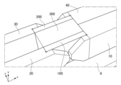
図1は、本発明の第1の実施形態による磁気センサ1の外観を示す略斜視図である。また、図2は磁気センサ1を別の角度から見た部分的な略斜視図であり、図3及び図4は磁気センサ1の略分解斜視図である。
FIG. 1 is a schematic perspective view showing the appearance of a
図1~図4に示すように、第1の実施形態による磁気センサ1は、基板8と、基板8に搭載されたセンサチップ100及び外部磁性体10,20とを備えている。基板8はxz面を主面とし、主面にセンサチップ100及び外部磁性体10,20が搭載されている。センサチップ100は、yz面を構成し互いに反対側に位置する側面101,102と、xz面を構成し互いに反対側に位置する側面103,104と、xy面を構成し互いに反対側に位置する素子形成面105及び裏面106とを有している。センサチップ100は、側面103が基板8の主面と向かい合うよう、基板8に立てて搭載されている。
As shown in FIGS. 1 to 4, the
外部磁性体10,20は、いずれもフェライトなどの高透磁率材料によって構成される。外部磁性体10は、x方向を長手方向とする棒状の本体部11と、本体部11のx方向における端部に設けられた突出部12からなる。同様に、外部磁性体20は、x方向を長手方向とする棒状の本体部21と、本体部21のx方向における端部に設けられた突出部22からなる。本体部11と突出部12は、一体的であっても構わないし、それぞれ別のブロックからなるものであっても構わない。本体部21と突出部22についても同様である。
Both the external
突出部12,22のz方向における厚みは、本体部11,21のz方向における厚みよりも薄い。これにより、突出部12にはxy面を構成する内面12aが形成され、本体部11のx方向における端部にはyz面を構成する内面11aが形成される。同様に、突出部22にはxy面を構成する内面22aが形成され、本体部21のx方向における端部にはyz面を構成する内面21aが形成される。
The thickness of the protruding
そして、図2及び図4に示すように、センサチップ100の側面101が外部磁性体10の内面11aで覆われ、センサチップ100の側面102が外部磁性体20の内面21aに覆われるよう、基板8上においてセンサチップ100と外部磁性体10,20が位置決めされる。つまり、センサチップ100と外部磁性体10のx方向における位置関係は、センサチップ100の側面101を外部磁性体10の内面11aに当接させることによって固定され、センサチップ100と外部磁性体20のx方向における位置関係は、センサチップ100の側面102を外部磁性体20の内面21aに当接させることによって固定される。これにより、突出部12と突出部22の間に形成される磁気ギャップG1のx方向における距離が固定される。また、センサチップ100と外部磁性体10,20をx方向に位置決めすると、センサチップ100の素子形成面105が外部磁性体10の内面12a及び外部磁性体20の内面22aで覆われる。
Then, as shown in FIGS. 2 and 4, the substrate is arranged so that the
さらに、外部磁性体10の内面11aと内面12aが突き当たる角部には、溝13が形成されている。同様に、外部磁性体20の内面12aと内面22aが突き当たる角部には、溝23が形成されている。これは、加工精度などに起因して上記角部が丸みを帯びると、丸みを帯びた角部とセンサチップ100が干渉し、センサチップ100を正しく位置決めできないからであり、溝13,23によって上記角部を除去することによってセンサチップ100を正しく位置決めすることが可能となる。
Further, a
また、センサチップ100は、側面103が基板8と向かい合うよう立てて搭載されることから、センサチップ100の厚みが薄い場合、強度が不足するおそれがある。このような場合には、図5に示すように、センサチップ100の裏面106に補助基板120を設けることによって強度を確保しても構わない。補助基板120は、接着剤などを用いて、センサチップ100及び基板8に固定することができる。補助基板120の材料としては、センサチップ100と同じ材料を用いても構わない。
Moreover, since the
図6は、センサチップ100の構造を説明するための略斜視図である。
FIG. 6 is a schematic perspective view for explaining the structure of the
図6に示すように、センサチップ100の素子形成面105上には感磁素子R1、磁性体層111,112、端子電極T11~T14が形成されている。磁性体層111,112は、パーマロイなどのNiFe系材料からなる薄膜であり、磁性体層111,112からなる磁気ギャップG2によって形成される磁路上に感磁素子R1が配置されている。
As shown in FIG. 6, on the
図7は、センサチップ100から磁性体層111,112を除去した状態を示す略斜視図である。
FIG. 7 is a schematic perspective view showing a state in which the
図7に示すように、感磁素子R1は、素子形成面105上においてy方向に延在し、その一端が配線L1を介して端子電極T11に接続され、他端が配線L2を介して端子電極T12に接続されている。感磁素子R1は、磁束の向きによって電気抵抗が変化する素子であれば特に限定されず、例えばMR素子などを用いることができる。感磁素子R1の感度軸方向である固定磁化方向はx方向である。端子電極T13,T14は、図示しない補償コイルに接続される。補償コイルは、感磁素子R1に印加される磁界を打ち消すことによって、いわゆるクローズドループ制御を行うために用いられる。そして、本実施形態においては、センサチップ100の側面103が基板8と向かい合うよう、センサチップ100を立てて搭載していることから、端子電極T11~T14と基板8の配線距離を短縮することができる。これにより、ハンダなどを用いて、基板8に設けられたランドパターンと端子電極T11~T14を直接接続することが可能となる。
As shown in FIG. 7, the magneto-sensitive element R1 extends in the y-direction on the
図8は、センサチップ100の主要部のxz断面図である。
FIG. 8 is an xz sectional view of the main part of the
図8に示すように、センサチップ100の素子形成面105には、感磁素子R1が形成されている。感磁素子R1は絶縁層107で覆われており、絶縁層107の表面に磁性体層111,112が形成されている。そして、平面視で(z方向から見て)、感磁素子R1は磁性体層111と磁性体層112の間に位置する。これにより、磁気ギャップG2を通過する磁界が感磁素子R1に印加される。つまり、感磁素子R1は、磁性体層111と磁性体層112によって形成される磁気ギャップG2の近傍であり、磁気ギャップG2を通過する検出対象磁界を検出可能な磁路上に配置される。このように、感磁素子R1を必ずしも2つの磁性体層111,112間に配置する必要はなく、磁性体層111,112からなる磁気ギャップG2を通過する磁界の少なくとも一部が感磁素子R1に印加されるような配置であれば足りる。磁気ギャップG2の幅と感磁素子R1の幅の関係については特に限定されない。図8に示す例では、磁気ギャップG2のx方向における幅G2xが感磁素子R1のx方向における幅Rxよりも狭く、これにより、z方向から見て磁性体層111,112と感磁素子R1が重なりOVを有している。磁気ギャップG2を通過する磁界のより多くを感磁素子R1に印加するためには、重なりOVにおける磁性体層111,112と感磁素子R1のz方向における距離ができるだけ近いことが望ましく、磁気ギャップG2のx方向における幅G2xよりも磁性体層111,112と感磁素子R1のz方向における距離が近いことがより望ましい。これにより、感磁素子R1が磁気ギャップG2を通過する磁界の主な磁路となる。
As shown in FIG. 8, the
図9は、磁気センサ1の主要部を拡大して示す略部分斜視図である。
FIG. 9 is a schematic partial perspective view showing an enlarged main part of the
図9に示すように、センサチップ100と外部磁性体10,20をx方向に位置決めすると、磁性体層111は外部磁性体10の内面12aと重なり、磁性体層112は外部磁性体20の内面22aと重なる。これにより、例えば外部磁性体10の本体部11によって集磁したx方向の磁束は、外部磁性体10の突出部12を介して磁性体層111に流れる。磁性体層111に流れた磁束は、磁気ギャップG2を介して磁性体層112に流れ、さらに、外部磁性体20の突出部22を介して本体部21に流れる。そして、外部磁性体10,20によって集磁したx方向の磁束が磁気ギャップG2を流れる際、感磁素子R1にx方向の磁束が印加されることから、例えば感磁素子R1の抵抗値の変化に基づいて磁束の向き及び量を検出することができる。
As shown in FIG. 9, when the
ここで、突出部12と突出部22によって形成される磁気ギャップG1のx方向における幅G1xは、磁性体層111と磁性体層112によって形成される磁気ギャップG2のx方向における幅G2xよりも十分に広いことが好ましい。これは、磁気ギャップG1の幅G1xが狭すぎると磁束が磁気ギャップG1間をバイパスし、感磁素子R1に印加される磁束が減少するからである。一例として、磁気ギャップG1の幅G1xは数百μm程度、磁気ギャップG2の幅G2xは数μm程度とすればよい。
Here, the width G1x in the x direction of the magnetic gap G1 formed by the
このように、本実施形態による磁気センサ1は、外部磁性体10,20によって集磁したx方向の磁束を曲げることなく、感度軸方向がx方向である感磁素子R1に印加することができることから、高い検出感度を得ることが可能となる。しかも、感磁素子R1が形成されたセンサチップ100と外部磁性体10,20がx方向に位置決めされることから、磁気ギャップG1の幅G1xにばらつきが生じにくく、これにより検出感度のばらつきを低減することができる。
As described above, the
また、外部磁性体10の内面12aや外部磁性体20の内面22aは、磁気ギャップG2に近づくにつれてy方向における幅が狭くなる形状を有していることから、感磁素子R1に印加される磁束密度をより高めることが可能となる。但し、外部磁性体10,20がこのような形状を有している点は必須でなく、内面12a,22aのy方向における幅が一定であっても構わない。これによれば、外部磁性体10,20の作製が容易となる。
In addition, since the
図10は、磁気ギャップG1の幅及び突出部12,22のz方向における厚みと感磁素子R1に印加される磁束密度との関係を示すグラフである。
FIG. 10 is a graph showing the relationship between the width of the magnetic gap G1, the thickness of the
図10に示すように、磁気ギャップG1が0.6mm以下の領域では磁気ギャップG1が狭いほど感磁素子R1に印加される磁束密度が高くなる。これは、磁気ギャップG1が狭いほど磁気抵抗が低くなるからである。一方、磁気ギャップG1が0.6mm未満になると、磁気ギャップG1が狭いほど感磁素子R1に印加される磁束密度が急速に低下する。これは、磁気ギャップG1が狭すぎると、外部磁性体10,20間において磁束がバイパスし、感磁素子R1に印加される磁束が減少するからである。また、突出部12,22のz方向における厚みについては、薄いほど感磁素子R1に印加される磁束密度が高くなる。これは、突出部12,22のz方向における厚みが薄いほど、外部磁性体10,20間における磁束のバイパスが生じにくくなるからである。
As shown in FIG. 10, in the region where the magnetic gap G1 is 0.6 mm or less, the narrower the magnetic gap G1, the higher the magnetic flux density applied to the magneto-sensitive element R1. This is because the narrower the magnetic gap G1, the lower the magnetic resistance. On the other hand, when the magnetic gap G1 is less than 0.6 mm, the narrower the magnetic gap G1, the more rapidly the magnetic flux density applied to the magneto-sensitive element R1 decreases. This is because if the magnetic gap G1 is too narrow, the magnetic flux bypasses between the external
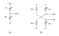
図11(a)に示すように、感磁素子R1と固定抵抗R10を電源間に直列に接続することにより、両者の接続点から検出信号V1を得ることができる。固定抵抗R10は、センサチップ100の素子形成面105に設けても構わないし、基板8に設けても構わない。固定抵抗R10をセンサチップ100の素子形成面105に設ける場合、感磁素子R1と同じ構成を有し、磁界によって抵抗値が変化しないダミー素子を固定抵抗R10として用いても構わない。また、図11(b)に示すように、感磁素子R1と固定抵抗R11~R13をブリッジ接続することによって検出信号V2,V3が得られるよう構成しても構わない。
As shown in FIG. 11(a), by connecting the magneto-sensitive element R1 and the fixed resistor R10 in series between the power supply, the detection signal V1 can be obtained from the connection point between the two. The fixed resistor R10 may be provided on the
図12は、本発明の第2の実施形態による磁気センサ2の外観を示す略斜視図である。また、図13及び図14は磁気センサ2の部分的な略分解斜視図である。
FIG. 12 is a schematic perspective view showing the appearance of the
図12~図14に示すように、第2の実施形態による磁気センサ2は、基板8に搭載されたセンサチップ200及び外部磁性体30,40をさらに備えている点において、第1の実施形態による磁気センサ1と相違している。その他の基本的な構成については、第1の実施形態による磁気センサ1と同一であることから、同一の要素には同一の符号を付し、重複する説明は省略する。
As shown in FIGS. 12 to 14, the
センサチップ200は、センサチップ100と同じ構造を有し、yz面を構成し互いに反対側に位置する側面201,202と、xz面を構成し互いに反対側に位置する側面203,204と、xy面を構成し互いに反対側に位置する素子形成面205及び裏面206とを有している。センサチップ200は、側面203が基板8の主面と向かい合うよう、基板8に搭載されている。
The
外部磁性体30,40は、いずれもフェライトなどの高透磁率材料によって構成され、それぞれ外部磁性体20,10と同じ構造を有している。外部磁性体30は、x方向を長手方向とする棒状の本体部31と、本体部31のx方向における端部に設けられた突出部32からなる。同様に、外部磁性体40は、x方向を長手方向とする棒状の本体部41と、本体部41のx方向における端部に設けられた突出部42からなる。そして、外部磁性体10,40はz方向に配列され、外部磁性体20,30はz方向に配列される。本実施形態においては、外部磁性体10,40の本体部11,41のz方向における厚みは、外部磁性体20,30の本体部21,31のz方向における厚みよりも厚い。外部磁性体10,40の本体部11,41が互い接しているのに対し、外部磁性体20,30の本体部21,31は互いにz方向に離間している。外部磁性体10,40については、単一のブロックからなるものであっても構わない。このような構成により、外部磁性体10,40の+x方向における先端部を検出ヘッドとし、x方向における磁束を集磁することができる。
Both the external
そして、図13及び図14に示すように、センサチップ200の側面201が外部磁性体30の内面31aで覆われ、センサチップ200の側面202が外部磁性体40の内面41aで覆われるよう、基板8上においてセンサチップ200と外部磁性体30,40が位置決めされる。つまり、センサチップ200と外部磁性体30のx方向における位置関係は、センサチップ200の側面201を外部磁性体30の内面31aに当接させることによって固定され、センサチップ200と外部磁性体40のx方向における位置関係は、センサチップ200の側面202を外部磁性体40の内面41aに当接させることによって固定される。これにより、突出部32と突出部42の間に形成される磁気ギャップのx方向における距離が固定される。また、センサチップ200と外部磁性体30,40をx方向に位置決めすると、センサチップ200の素子形成面205が外部磁性体30の内面32a及び外部磁性体40の内面42aで覆われる。
Then, as shown in FIGS. 13 and 14 , the substrate is arranged such that the
センサチップ200の素子形成面205上には感磁素子R2、磁性体層211,212が形成されている。磁性体層211,212は、パーマロイなどのNiFe系材料からなる薄膜であり、磁性体層211,212からなる磁気ギャップによって形成される磁路上に感磁素子R2が配置されている。そして、センサチップ200と外部磁性体30,40をx方向に位置決めすると、磁性体層211は外部磁性体30の内面32aと重なり、磁性体層212は外部磁性体40の内面42aと重なる。
A magneto-sensitive element R2 and
そして、センサチップ100とセンサチップ200は、裏面106,206同士が向かい合うよう配置されている。これにより、感磁素子R1と感磁素子R2の感度軸方向は、互いに180°異なることになる。例えば、感磁素子R1の感度軸方向が+x方向であれば、感磁素子R2の感度軸方向は-x方向となる。このため、図15(a)に示すように、感磁素子R1と感磁素子R2を電源間に直列に接続することにより、両者の接続点からより振幅の大きい検出信号V4を得ることができる。また、図15(b)に示すように、感磁素子R1,R2と固定抵抗R14,R15をブリッジ接続することによって差動信号V5,V6が得られるよう構成しても構わない。さらに、感磁素子R1,R2をそれぞれブリッジ接続することによってダブルフルブリッジを構成しても構わない。
The
また、図16に示すように、センサチップ100とセンサチップ200の間に、裏面106,206と接するスペーサー300を設けても構わない。これによれば、スペーサー300を介した熱伝導により、センサチップ100とセンサチップ200の温度差が小さくなることから、温度差に起因する測定誤差を低減することが可能となる。しかも、センサチップ100,200の裏面106,206がスペーサー300で覆われることから、全体の機械的強度も高められる。
Further, as shown in FIG. 16, a
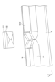
図17は、本発明の第3の実施形態による磁気センサ3の外観を示す略斜視図である。また、図18は磁気センサ3の部分的な略分解斜視図である。
FIG. 17 is a schematic perspective view showing the external appearance of the
図17及び図18に示すように、第3の実施形態による磁気センサ3は、センサチップ100の裏面106とセンサチップ200の裏面206が互いに接しているとともに、外部磁性体20,30の本体部21,31が接している点において、第2の実施形態による磁気センサ2と相違している。その他の基本的な構成については、第2の実施形態による磁気センサ2と同一であることから、同一の要素には同一の符号を付し、重複する説明は省略する。
As shown in FIGS. 17 and 18, in the
第3の実施形態による磁気センサ3のように、センサチップ100,200の裏面106,206を互いに接触させれば、センサチップ100とセンサチップ200の温度差がより小さくなることから、温度差に起因する測定誤差をより低減することが可能となる。本実施形態においても、外部磁性体10,40が単一のブロックからなるものであっても構わないし、外部磁性体20,30が単一のブロックからなるものであっても構わない。
If the
以上、本発明の好ましい実施形態について説明したが、本発明は、上記の実施形態に限定されることなく、本発明の主旨を逸脱しない範囲で種々の変更が可能であり、それらも本発明の範囲内に包含されるものであることはいうまでもない。 Although the preferred embodiments of the present invention have been described above, the present invention is not limited to the above-described embodiments, and various modifications can be made without departing from the gist of the present invention. Needless to say, it is included within the scope.
1~3 磁気センサ
8 基板
10,20,30,40 外部磁性体
11,21,31,41 本体部
12,22,32,42 突出部
11a,12a,21a,22a,31a,32a,41a,42a 内面
13,23 溝
100,200 センサチップ
101~104,201~204 側面
105,205 素子形成面
106,206 裏面
107 絶縁層
111,112,211,212 磁性体層
120 補助基板
300 スペーサー
G1,G2 磁気ギャップ
L1,L2 配線
R1,R2 感磁素子
R10~R15 固定抵抗
T11~T14 端子電極
1 to 3
Claims (9)
前記第1の方向を長手方向とする第1及び第2の外部磁性体と、を備え、
前記素子形成面上には、第1の磁気ギャップを介して前記第1の方向に配列された第1及び第2の磁性体層と、前記第1の磁気ギャップによって形成される磁路上に配置され、前記第1の方向を感磁方向とする第1の感磁素子とが形成され、
前記第1の外部磁性体は、前記第1の磁性体層と重なるよう前記素子形成面を覆う第1の内面と、前記第1の側面を覆う第2の内面を有し、
前記第2の外部磁性体は、前記第2の磁性体層と重なるよう前記素子形成面を覆う第3の内面と、前記第2の側面を覆う第4の内面を有することを特徴とする磁気センサ。 an element forming surface extending in a first direction and a second direction perpendicular to the first direction; and first and second side surfaces perpendicular to the first direction and parallel to each other a first sensor chip having
First and second external magnetic bodies having the first direction as a longitudinal direction,
On the element formation surface, first and second magnetic layers arranged in the first direction with a first magnetic gap interposed therebetween, and arranged on a magnetic path formed by the first magnetic gap a first magneto-sensitive element having the first direction as a magneto-sensitive direction;
The first external magnetic body has a first inner surface covering the element formation surface so as to overlap with the first magnetic layer and a second inner surface covering the first side surface,
The second external magnetic body has a third inner surface covering the element forming surface so as to overlap with the second magnetic layer, and a fourth inner surface covering the second side surface. sensor.
前記第2の外部磁性体は、前記第3の内面と前記第4の内面が突き当たる角部が除去された構造を有していることを特徴とする請求項1又は2に記載の磁気センサ。 The first external magnetic body has a structure in which corners where the first inner surface and the second inner surface meet are removed,
3. The magnetic sensor according to claim 1, wherein the second external magnetic body has a structure in which corners where the third inner surface and the fourth inner surface meet are removed.
前記第1のセンサチップは、前記第2の方向に対して垂直な第3の側面が前記基板と向かい合うよう搭載されていることを特徴とする請求項1乃至3のいずれか一項に記載の磁気センサ。 further comprising a substrate on which the first sensor chip, the first external magnetic body and the second external magnetic body are mounted;
4. The first sensor chip according to any one of claims 1 to 3, wherein said first sensor chip is mounted so that a third side surface perpendicular to said second direction faces said substrate. magnetic sensor.
前記第1の方向を長手方向とする第3及び第4の外部磁性体と、をさらに備え、
前記第2のセンサチップの前記素子形成面上には、第2の磁気ギャップを介して前記第1の方向に配列された第3及び第4の磁性体層と、前記第2の磁気ギャップによって形成される磁路上に配置され、前記第1の方向を感磁方向とする第2の感磁素子とが形成され、
前記第3の外部磁性体は、前記第3の磁性体層と重なるよう前記素子形成面を覆う第5の内面と、前記第4の側面を覆う第6の内面を有し、
前記第4の外部磁性体は、前記第4の磁性体層と重なるよう前記素子形成面を覆う第7の内面と、前記第5の側面を覆う第8の内面を有し、
前記第1の感磁素子と前記第2の感磁素子の感度軸方向は、互いに180°異なっていることを特徴とする請求項1乃至4のいずれか一項に記載の磁気センサ。 a second sensor chip having an element forming surface extending in the first and second directions, and fourth and fifth side surfaces perpendicular to the first direction and parallel to each other;
Further comprising third and fourth external magnetic bodies having the first direction as a longitudinal direction,
On the element forming surface of the second sensor chip, third and fourth magnetic layers arranged in the first direction with a second magnetic gap interposed therebetween, and the second magnetic gap a second magneto-sensitive element disposed on the formed magnetic path and having the first direction as a magneto-sensitive direction;
the third external magnetic body has a fifth inner surface covering the element forming surface so as to overlap with the third magnetic layer and a sixth inner surface covering the fourth side surface;
The fourth external magnetic body has a seventh inner surface covering the element formation surface so as to overlap with the fourth magnetic layer and an eighth inner surface covering the fifth side surface,
5. A magnetic sensor according to claim 1, wherein the sensitivity axis directions of said first magneto-sensitive element and said second magneto-sensitive element are different from each other by 180[deg.].
Priority Applications (2)
| Application Number | Priority Date | Filing Date | Title |
|---|---|---|---|
| JP2021125510A JP7638819B2 (en) | 2021-07-30 | 2021-07-30 | Magnetic Sensor |
| PCT/JP2022/024685 WO2023007989A1 (en) | 2021-07-30 | 2022-06-21 | Magnetic sensor |
Applications Claiming Priority (1)
| Application Number | Priority Date | Filing Date | Title |
|---|---|---|---|
| JP2021125510A JP7638819B2 (en) | 2021-07-30 | 2021-07-30 | Magnetic Sensor |
Publications (2)
| Publication Number | Publication Date |
|---|---|
| JP2023020249A true JP2023020249A (en) | 2023-02-09 |
| JP7638819B2 JP7638819B2 (en) | 2025-03-04 |
Family
ID=85086604
Family Applications (1)
| Application Number | Title | Priority Date | Filing Date |
|---|---|---|---|
| JP2021125510A Active JP7638819B2 (en) | 2021-07-30 | 2021-07-30 | Magnetic Sensor |
Country Status (2)
| Country | Link |
|---|---|
| JP (1) | JP7638819B2 (en) |
| WO (1) | WO2023007989A1 (en) |
Cited By (1)
| Publication number | Priority date | Publication date | Assignee | Title |
|---|---|---|---|---|
| CN119247219A (en) * | 2024-08-30 | 2025-01-03 | 北京智芯微电子科技有限公司 | Magnetic sensor chip sensitivity temperature drift test device and test method |
Citations (6)
| Publication number | Priority date | Publication date | Assignee | Title |
|---|---|---|---|---|
| US20100271018A1 (en) * | 2009-04-24 | 2010-10-28 | Seagate Technology Llc | Sensors for minute magnetic fields |
| JP2016164549A (en) * | 2015-02-26 | 2016-09-08 | エスアイアイ・セミコンダクタ株式会社 | Magnetic sensor and manufacturing method therefor |
| WO2018216651A1 (en) * | 2017-05-23 | 2018-11-29 | Tdk株式会社 | Magnetic sensor |
| JP2019215311A (en) * | 2018-06-07 | 2019-12-19 | Tdk株式会社 | Magnetic sensor |
| JP2020187084A (en) * | 2019-05-17 | 2020-11-19 | Tdk株式会社 | Magnetic sensor |
| JP2021105601A (en) * | 2019-12-27 | 2021-07-26 | Tdk株式会社 | Magnetic sensor |
-
2021
- 2021-07-30 JP JP2021125510A patent/JP7638819B2/en active Active
-
2022
- 2022-06-21 WO PCT/JP2022/024685 patent/WO2023007989A1/en not_active Ceased
Patent Citations (6)
| Publication number | Priority date | Publication date | Assignee | Title |
|---|---|---|---|---|
| US20100271018A1 (en) * | 2009-04-24 | 2010-10-28 | Seagate Technology Llc | Sensors for minute magnetic fields |
| JP2016164549A (en) * | 2015-02-26 | 2016-09-08 | エスアイアイ・セミコンダクタ株式会社 | Magnetic sensor and manufacturing method therefor |
| WO2018216651A1 (en) * | 2017-05-23 | 2018-11-29 | Tdk株式会社 | Magnetic sensor |
| JP2019215311A (en) * | 2018-06-07 | 2019-12-19 | Tdk株式会社 | Magnetic sensor |
| JP2020187084A (en) * | 2019-05-17 | 2020-11-19 | Tdk株式会社 | Magnetic sensor |
| JP2021105601A (en) * | 2019-12-27 | 2021-07-26 | Tdk株式会社 | Magnetic sensor |
Cited By (1)
| Publication number | Priority date | Publication date | Assignee | Title |
|---|---|---|---|---|
| CN119247219A (en) * | 2024-08-30 | 2025-01-03 | 北京智芯微电子科技有限公司 | Magnetic sensor chip sensitivity temperature drift test device and test method |
Also Published As
| Publication number | Publication date |
|---|---|
| WO2023007989A1 (en) | 2023-02-02 |
| JP7638819B2 (en) | 2025-03-04 |
Similar Documents
| Publication | Publication Date | Title |
|---|---|---|
| JP5012939B2 (en) | Current sensor | |
| JP6822127B2 (en) | Magnetic sensor | |
| CN107430155A (en) | current sensor | |
| JP2009002911A (en) | Current sensor and manufacturing method thereof | |
| CN110709720B (en) | Magnetic sensor | |
| JP2006125962A (en) | Current sensor | |
| CN120044455A (en) | Magnetic sensor | |
| CN111198341B (en) | Magnetic sensor and position detection device | |
| JP7070532B2 (en) | Magnetic sensor | |
| JP7095350B2 (en) | Magnetic sensor | |
| CN113474670A (en) | Magnetic sensor and method for manufacturing the same | |
| WO2019167598A1 (en) | Magnetic sensor | |
| JP2019144116A (en) | Magnetic sensor | |
| WO2023007989A1 (en) | Magnetic sensor | |
| WO2023145063A1 (en) | Magnetic sensor | |
| JP7628832B2 (en) | Magnetic Sensors | |
| JP2023060610A (en) | magnetic sensor | |
| JP2022143682A (en) | magnetic sensor | |
| JP7521981B2 (en) | Magnetic Sensors | |
| CN108780130B (en) | Magnetic sensor | |
| US12174270B2 (en) | Magnetic sensor | |
| WO2011111747A1 (en) | Current sensor provided with magnetic detection element | |
| JP2013047610A (en) | Magnetic balance type current sensor | |
| JP7832340B2 (en) | Magnetic sensor | |
| CN116075735B (en) | Magnetic sensor and method for manufacturing the same |
Legal Events
| Date | Code | Title | Description |
|---|---|---|---|
| A521 | Request for written amendment filed |
Free format text: JAPANESE INTERMEDIATE CODE: A523 Effective date: 20220602 |
|
| A521 | Request for written amendment filed |
Free format text: JAPANESE INTERMEDIATE CODE: A821 Effective date: 20220602 |
|
| A621 | Written request for application examination |
Free format text: JAPANESE INTERMEDIATE CODE: A621 Effective date: 20240516 |
|
| TRDD | Decision of grant or rejection written | ||
| A01 | Written decision to grant a patent or to grant a registration (utility model) |
Free format text: JAPANESE INTERMEDIATE CODE: A01 Effective date: 20250212 |
|
| A61 | First payment of annual fees (during grant procedure) |
Free format text: JAPANESE INTERMEDIATE CODE: A61 Effective date: 20250219 |
|
| R150 | Certificate of patent or registration of utility model |
Ref document number: 7638819 Country of ref document: JP Free format text: JAPANESE INTERMEDIATE CODE: R150 |