JP2009002911A - Current sensor and method of manufacturing therefor - Google Patents
Current sensor and method of manufacturing therefor Download PDFInfo
- Publication number
- JP2009002911A JP2009002911A JP2007166576A JP2007166576A JP2009002911A JP 2009002911 A JP2009002911 A JP 2009002911A JP 2007166576 A JP2007166576 A JP 2007166576A JP 2007166576 A JP2007166576 A JP 2007166576A JP 2009002911 A JP2009002911 A JP 2009002911A
- Authority
- JP
- Japan
- Prior art keywords
- magnetic field
- current sensor
- magnetoresistive
- elements
- layer
- Prior art date
- Legal status (The legal status is an assumption and is not a legal conclusion. Google has not performed a legal analysis and makes no representation as to the accuracy of the status listed.)
- Granted
Links
- 238000004519 manufacturing process Methods 0.000 title claims description 22
- 230000005291 magnetic effect Effects 0.000 claims abstract description 260
- 230000005415 magnetization Effects 0.000 claims abstract description 100
- 239000000758 substrate Substances 0.000 claims abstract description 96
- 238000001514 detection method Methods 0.000 claims abstract description 60
- 230000000694 effects Effects 0.000 claims description 76
- 230000006698 induction Effects 0.000 claims description 47
- 239000004020 conductor Substances 0.000 claims description 37
- 230000008859 change Effects 0.000 claims description 32
- 230000005294 ferromagnetic effect Effects 0.000 claims description 18
- 230000008878 coupling Effects 0.000 claims description 7
- 238000010168 coupling process Methods 0.000 claims description 7
- 238000005859 coupling reaction Methods 0.000 claims description 7
- 239000010409 thin film Substances 0.000 abstract description 52
- 125000006850 spacer group Chemical group 0.000 abstract description 5
- 238000010030 laminating Methods 0.000 abstract description 3
- 230000001939 inductive effect Effects 0.000 abstract 1
- 239000010410 layer Substances 0.000 description 162
- 239000010408 film Substances 0.000 description 39
- 238000000034 method Methods 0.000 description 16
- 238000004804 winding Methods 0.000 description 14
- 239000010949 copper Substances 0.000 description 7
- 230000008569 process Effects 0.000 description 7
- 230000007423 decrease Effects 0.000 description 6
- 238000005259 measurement Methods 0.000 description 6
- 230000035945 sensitivity Effects 0.000 description 6
- 239000013598 vector Substances 0.000 description 6
- RYGMFSIKBFXOCR-UHFFFAOYSA-N Copper Chemical compound [Cu] RYGMFSIKBFXOCR-UHFFFAOYSA-N 0.000 description 5
- 229910052802 copper Inorganic materials 0.000 description 5
- 238000010586 diagram Methods 0.000 description 5
- 229920006395 saturated elastomer Polymers 0.000 description 5
- 230000005290 antiferromagnetic effect Effects 0.000 description 4
- 238000009826 distribution Methods 0.000 description 4
- 230000004044 response Effects 0.000 description 4
- 229910018072 Al 2 O 3 Inorganic materials 0.000 description 3
- 229910001030 Iron–nickel alloy Inorganic materials 0.000 description 3
- XUIMIQQOPSSXEZ-UHFFFAOYSA-N Silicon Chemical compound [Si] XUIMIQQOPSSXEZ-UHFFFAOYSA-N 0.000 description 3
- 239000013078 crystal Substances 0.000 description 3
- 239000000696 magnetic material Substances 0.000 description 3
- 239000000463 material Substances 0.000 description 3
- 229910052710 silicon Inorganic materials 0.000 description 3
- 239000010703 silicon Substances 0.000 description 3
- 229910003321 CoFe Inorganic materials 0.000 description 2
- 229910000914 Mn alloy Inorganic materials 0.000 description 2
- 239000012790 adhesive layer Substances 0.000 description 2
- 239000010931 gold Substances 0.000 description 2
- 239000007769 metal material Substances 0.000 description 2
- 230000004048 modification Effects 0.000 description 2
- 238000012986 modification Methods 0.000 description 2
- TWNQGVIAIRXVLR-UHFFFAOYSA-N oxo(oxoalumanyloxy)alumane Chemical compound O=[Al]O[Al]=O TWNQGVIAIRXVLR-UHFFFAOYSA-N 0.000 description 2
- 238000007747 plating Methods 0.000 description 2
- 230000001681 protective effect Effects 0.000 description 2
- 230000004043 responsiveness Effects 0.000 description 2
- 229910001313 Cobalt-iron alloy Inorganic materials 0.000 description 1
- 240000006829 Ficus sundaica Species 0.000 description 1
- 230000002411 adverse Effects 0.000 description 1
- 238000000137 annealing Methods 0.000 description 1
- 239000002885 antiferromagnetic material Substances 0.000 description 1
- 229910017052 cobalt Inorganic materials 0.000 description 1
- 239000010941 cobalt Substances 0.000 description 1
- GUTLYIVDDKVIGB-UHFFFAOYSA-N cobalt atom Chemical compound [Co] GUTLYIVDDKVIGB-UHFFFAOYSA-N 0.000 description 1
- 238000005520 cutting process Methods 0.000 description 1
- 239000003302 ferromagnetic material Substances 0.000 description 1
- 230000004907 flux Effects 0.000 description 1
- PCHJSUWPFVWCPO-UHFFFAOYSA-N gold Chemical compound [Au] PCHJSUWPFVWCPO-UHFFFAOYSA-N 0.000 description 1
- 229910052737 gold Inorganic materials 0.000 description 1
- 229910052735 hafnium Inorganic materials 0.000 description 1
- VBJZVLUMGGDVMO-UHFFFAOYSA-N hafnium atom Chemical compound [Hf] VBJZVLUMGGDVMO-UHFFFAOYSA-N 0.000 description 1
- 230000006872 improvement Effects 0.000 description 1
- 238000009413 insulation Methods 0.000 description 1
- SHMWNGFNWYELHA-UHFFFAOYSA-N iridium manganese Chemical compound [Mn].[Ir] SHMWNGFNWYELHA-UHFFFAOYSA-N 0.000 description 1
- IGOJMROYPFZEOR-UHFFFAOYSA-N manganese platinum Chemical compound [Mn].[Pt] IGOJMROYPFZEOR-UHFFFAOYSA-N 0.000 description 1
- 238000000206 photolithography Methods 0.000 description 1
- 238000004544 sputter deposition Methods 0.000 description 1
- 229910052715 tantalum Inorganic materials 0.000 description 1
- GUVRBAGPIYLISA-UHFFFAOYSA-N tantalum atom Chemical compound [Ta] GUVRBAGPIYLISA-UHFFFAOYSA-N 0.000 description 1
Images


Classifications
-
- G—PHYSICS
- G01—MEASURING; TESTING
- G01R—MEASURING ELECTRIC VARIABLES; MEASURING MAGNETIC VARIABLES
- G01R33/00—Arrangements or instruments for measuring magnetic variables
- G01R33/02—Measuring direction or magnitude of magnetic fields or magnetic flux
- G01R33/06—Measuring direction or magnitude of magnetic fields or magnetic flux using galvano-magnetic devices
- G01R33/09—Magnetoresistive devices
- G01R33/093—Magnetoresistive devices using multilayer structures, e.g. giant magnetoresistance sensors
-
- B—PERFORMING OPERATIONS; TRANSPORTING
- B82—NANOTECHNOLOGY
- B82Y—SPECIFIC USES OR APPLICATIONS OF NANOSTRUCTURES; MEASUREMENT OR ANALYSIS OF NANOSTRUCTURES; MANUFACTURE OR TREATMENT OF NANOSTRUCTURES
- B82Y25/00—Nanomagnetism, e.g. magnetoimpedance, anisotropic magnetoresistance, giant magnetoresistance or tunneling magnetoresistance
-
- G—PHYSICS
- G01—MEASURING; TESTING
- G01R—MEASURING ELECTRIC VARIABLES; MEASURING MAGNETIC VARIABLES
- G01R15/00—Details of measuring arrangements of the types provided for in groups G01R17/00 - G01R29/00, G01R33/00 - G01R33/26 or G01R35/00
- G01R15/14—Adaptations providing voltage or current isolation, e.g. for high-voltage or high-current networks
- G01R15/20—Adaptations providing voltage or current isolation, e.g. for high-voltage or high-current networks using galvano-magnetic devices, e.g. Hall-effect devices, i.e. measuring a magnetic field via the interaction between a current and a magnetic field, e.g. magneto resistive or Hall effect devices
- G01R15/205—Adaptations providing voltage or current isolation, e.g. for high-voltage or high-current networks using galvano-magnetic devices, e.g. Hall-effect devices, i.e. measuring a magnetic field via the interaction between a current and a magnetic field, e.g. magneto resistive or Hall effect devices using magneto-resistance devices, e.g. field plates
-
- H—ELECTRICITY
- H01—ELECTRIC ELEMENTS
- H01F—MAGNETS; INDUCTANCES; TRANSFORMERS; SELECTION OF MATERIALS FOR THEIR MAGNETIC PROPERTIES
- H01F10/00—Thin magnetic films, e.g. of one-domain structure
- H01F10/32—Spin-exchange-coupled multilayers, e.g. nanostructured superlattices
- H01F10/324—Exchange coupling of magnetic film pairs via a very thin non-magnetic spacer, e.g. by exchange with conduction electrons of the spacer
- H01F10/3268—Exchange coupling of magnetic film pairs via a very thin non-magnetic spacer, e.g. by exchange with conduction electrons of the spacer the exchange coupling being asymmetric, e.g. by use of additional pinning, by using antiferromagnetic or ferromagnetic coupling interface, i.e. so-called spin-valve [SV] structure, e.g. NiFe/Cu/NiFe/FeMn
-
- H—ELECTRICITY
- H01—ELECTRIC ELEMENTS
- H01F—MAGNETS; INDUCTANCES; TRANSFORMERS; SELECTION OF MATERIALS FOR THEIR MAGNETIC PROPERTIES
- H01F17/00—Fixed inductances of the signal type
- H01F17/0006—Printed inductances
- H01F17/0033—Printed inductances with the coil helically wound around a magnetic core
Abstract
Description
本発明は、導体を流れる電流の変化を高感度に検出可能な電流センサおよびその製造方法に関する。 The present invention relates to a current sensor capable of detecting a change in current flowing through a conductor with high sensitivity and a method for manufacturing the current sensor.
一般に、制御機器の回路に流れる制御電流を正確に測定するにあたっては、その回路内に抵抗を直列接続し、この抵抗の電圧降下を測定する方法を用いる。しかし、この場合には、制御系とは異なる負荷が加わることとなり制御系に対して何らかの悪影響を与える可能性が生じてしまう。このため、制御電流によって発生する電流磁界の勾配を検出することによって間接的に測定する方法が用いられている。具体的には、U字状の湾曲導体に制御電流を供給し、その湾曲導体の周囲に生じる電流磁界の変化をホール素子によって検出するする方法である(例えば、特許文献1参照)。
しかし、上記のような電流センサでは、小型化が困難であることに加え、磁界変化に対する検出感度の直線性あるいは高周波応答性の面で不十分であるなどの問題点が指摘されるようになった。このため、ホール素子の替わりに巨大磁気抵抗効果(Giant Magneto-Resistive effect)を発現する巨大磁気抵抗効果素子(以下、GMR素子)を制御電流による電流磁界中に配置し、その勾配を検出するようにした電流センサが提案されている。このようなGMR素子を用いた電流センサであれば、検出感度や応答性が向上するうえ、温度変化に対しても安定した検出特性が得られる。 However, in the current sensor as described above, problems such as difficulty in miniaturization and inadequate detection sensitivity linearity or high frequency response to a magnetic field change have been pointed out. It was. Therefore, instead of the Hall element, a giant magnetoresistive effect element (hereinafter referred to as GMR element) that exhibits a giant magnetoresistive effect is arranged in the current magnetic field by the control current, and the gradient is detected. A current sensor has been proposed. A current sensor using such a GMR element can improve detection sensitivity and responsiveness, and obtain stable detection characteristics against temperature changes.
ところで、最近では、より微弱な磁束や電流の検出が可能であると共によりいっそうコンパクトな全体構成を有する磁気センサや電流センサが強く求められるようになっている。しかしながら、GMR素子を用いた磁気センサや電流センサであっても、寸法の小型化に伴い、外部からのノイズ(不要な磁界など)の影響を受けやすくなるので、検出感度や応答性の面での安定性向上が課題となっている。これまでにも、GMR素子の形状を細長い短冊状として形状異方性を高めるなど、いくつかの試みがなされているが、十分に安定した性能レベルに達しているとは言い難い状況である。 Recently, there has been a strong demand for magnetic sensors and current sensors that can detect weaker magnetic fluxes and currents and have a more compact overall configuration. However, even magnetic sensors and current sensors using GMR elements are more susceptible to external noise (unnecessary magnetic fields, etc.) as their dimensions are reduced, so that detection sensitivity and responsiveness are reduced. Improvement of stability is a challenge. Some attempts have been made so far, such as increasing the shape anisotropy by making the shape of the GMR element into a long and narrow strip, but it is difficult to say that the performance level is sufficiently stable.
本発明はかかる問題に鑑みてなされたもので、その第1の目的は、検出対象電流による誘導磁界をより高精度に検出可能な電流センサを提供することにある。さらに、本発明の第2の目的は、そのような電流センサを効率的に製造する方法を提供することにある。 The present invention has been made in view of such a problem, and a first object thereof is to provide a current sensor capable of detecting an induced magnetic field caused by a detection target current with higher accuracy. Furthermore, a second object of the present invention is to provide a method for efficiently manufacturing such a current sensor.
本発明の第1の電流センサは、検出対象電流の供給により誘導磁界を発生する導体の近傍に配置され、その検出対象電流を検出するものであって、一定方向に固着された磁化方向を有する固着層と、非磁性の中間層と、誘導磁界に応じて磁化方向が変化すると共に固着層の磁化方向と異なる方向の異方性磁界を発現する自由層とを含む積層構造をそれぞれ有する第1および第2の磁気抵抗効果素子を備えるようにしたものである。ここで、第1および第2の磁気抵抗効果素子における各積層構造が、その積層面に沿った同一階層に設けられ、第1の磁気抵抗効果素子の抵抗値と第2の磁気抵抗効果素子の抵抗値とが誘導磁界に応じて互いに逆方向に変化するようになっている。本発明における異方性磁界とは、結晶構造や形状などに起因する全ての異方性磁界を意味する。また、「逆方向」とは、抵抗値の増減の方向が逆であることを意味する。したがって、第1の磁気抵抗効果素子の抵抗値が増加したときには第2の磁気抵抗効果素子の抵抗値は減少し、第1の磁気抵抗効果素子の抵抗値が減少したときには第2の磁気抵抗効果素子の抵抗値は増加する、という関係にある。 The first current sensor of the present invention is arranged in the vicinity of a conductor that generates an induced magnetic field by supplying a detection target current, detects the detection target current, and has a magnetization direction fixed in a certain direction. Each of the stacked structures includes a pinned layer, a nonmagnetic intermediate layer, and a free layer that changes its magnetization direction in response to an induced magnetic field and develops an anisotropic magnetic field in a direction different from the magnetization direction of the pinned layer. And a second magnetoresistance effect element. Here, each laminated structure in the first and second magnetoresistive elements is provided in the same layer along the laminated surface, and the resistance value of the first magnetoresistive element and the second magnetoresistive element are The resistance value changes in the opposite direction according to the induced magnetic field. The anisotropic magnetic field in this invention means all the anisotropic magnetic fields resulting from a crystal structure, a shape, etc. The “reverse direction” means that the direction of increase / decrease in resistance value is opposite. Therefore, when the resistance value of the first magnetoresistive element increases, the resistance value of the second magnetoresistive element decreases, and when the resistance value of the first magnetoresistive element decreases, the second magnetoresistive effect. There is a relationship that the resistance value of the element increases.
本発明の第2の電流センサは、検出対象電流の供給により誘導磁界を発生する導体の近傍に配置され、検出対象電流を検出する電流センサであって、一定方向に固着された磁化方向を有する固着層と、非磁性の中間層と、誘導磁界に応じて磁化方向が変化すると共に固着層の磁化方向と異なる方向の異方性磁界を発現する自由層とを含む積層構造をそれぞれ有する第1から第4の磁気抵抗効果素子を備えるようにしたものである。ここで、第1から第4の磁気抵抗効果素子における各積層構造が、その積層面に沿った同一階層に設けられており、第1の磁気抵抗効果素子の抵抗値と第3の磁気抵抗効果素子の抵抗値とが、誘導磁界に応じて互いに同方向に変化し、第2および第4の磁気抵抗効果素子の抵抗値が、誘導磁界に応じて第1および第3の磁気抵抗効果素子の抵抗値と逆方向に変化するようになっている。 A second current sensor of the present invention is a current sensor that is disposed in the vicinity of a conductor that generates an induced magnetic field by supplying a detection target current and detects the detection target current, and has a magnetization direction fixed in a certain direction. Each of the stacked structures includes a pinned layer, a nonmagnetic intermediate layer, and a free layer that changes its magnetization direction in response to an induced magnetic field and develops an anisotropic magnetic field in a direction different from the magnetization direction of the pinned layer. To a fourth magnetoresistive effect element. Here, each laminated structure in the first to fourth magnetoresistive effect elements is provided in the same layer along the laminated surface, and the resistance value of the first magnetoresistive effect element and the third magnetoresistive effect are provided. The resistance value of the element changes in the same direction according to the induced magnetic field, and the resistance value of the second and fourth magnetoresistive effect elements changes according to the induced magnetic field. It changes in the direction opposite to the resistance value.
本発明の第1または第2の電流センサでは、第1および第2の磁気抵抗効果素子(または第1から第4の磁気抵抗効果素子)における各積層構造が同一階層に設けられている。具体的には、各積層構造の厚み方向において、各積層構造の一方の表面同士および他方の表面同士がそれぞれ完全に一致し、または、各積層構造の一部が互いに等しい高さ位置にある。すなわち、各積層構造は、厚み方向と直交する方向へ平行移動した際に(積層面と平行に移動した際に)少なくともその一部が重なり合う位置関係にある。このような構成により、第1および第2の磁気抵抗効果素子における各積層構造を、検出対象電流が供給される導体に対して全て等しい距離に配置することが比較的容易となる。したがって、それらの積層構造が互いに異なる階層に位置する場合と比べ、導体へ検出対象電流が供給された際に各積層構造に対して付与される誘導磁界の差分が小さくなる。 In the first or second current sensor of the present invention, the stacked structures of the first and second magnetoresistive elements (or the first to fourth magnetoresistive elements) are provided on the same level. Specifically, in the thickness direction of each laminated structure, one surface and the other surface of each laminated structure are completely coincided with each other, or a part of each laminated structure is at the same height position. That is, each laminated structure has a positional relationship in which at least a part thereof overlaps when translated in a direction orthogonal to the thickness direction (when moved in parallel with the laminated surface). With such a configuration, it is relatively easy to arrange the laminated structures of the first and second magnetoresistive elements at the same distance from the conductor to which the detection target current is supplied. Therefore, the difference between the induced magnetic fields applied to each stacked structure when the detection target current is supplied to the conductor is smaller than when the stacked structures are located in different layers.
本発明の第1の電流センサでは、第1および第2の磁気抵抗効果素子における各自由層が全て同一階層に位置することが望ましい。同様に、本発明の第2の電流センサでは、第1から第4の磁気抵抗効果素子における各自由層が全て同一階層に位置することが望ましい。 In the first current sensor of the present invention, it is desirable that all the free layers in the first and second magnetoresistive elements are located in the same layer. Similarly, in the second current sensor of the present invention, it is desirable that all the free layers in the first to fourth magnetoresistive effect elements are located in the same layer.
本発明の第1の電流センサでは、第1の磁気抵抗効果素子の積層構造と、第2の磁気抵抗効果素子の積層構造とが、それらの積層面と平行な中心軸を回転中心として互いに回転対称な関係にあることが望ましい。本発明における「回転対称な関係」とは、磁化の大きさや方向を含めて構造上の対称性を有する関係を意味する。詳細には、第1の磁気抵抗効果素子の積層構造が回転中心軸を中心として180°回転(製造誤差程度のずれを含む)したときに、第2の磁気抵抗効果素子の積層構造と等価な関係となることをいう。ここでいう等価な関係とは、そのままの状態で、あるいは、一方が平行移動すれば互いに重なり合う(一致する)構造を有する関係を意味する。このような構成とすれば、第1および第2の磁気抵抗効果素子において、自由層の異方性磁界の方向と固着層の磁化方向との相対角度が互いに等しくなる。すなわち、自由層の磁化方向と固着層の磁化方向との初期状態での相対角度が互いに等しくなる。なお、初期状態とは、第1および第2の磁気抵抗効果素子に対し、導体から生じる誘導磁界を含む外部磁界が何ら付与されていない状態を意味する。この初期状態は、例えば、自由層の磁化が飽和する磁界と同等以上の大きさを有するバイアス磁界(リフレッシュ磁界ともいう。)を、第1および第2の磁気抵抗効果素子の双方に対して回転中心軸に沿って印加することで得られる。 In the first current sensor of the present invention, the laminated structure of the first magnetoresistive effect element and the laminated structure of the second magnetoresistive effect element rotate with respect to each other about a central axis parallel to the laminated surface. It is desirable to have a symmetric relationship. The “rotationally symmetric relationship” in the present invention means a relationship having structural symmetry including the magnitude and direction of magnetization. Specifically, when the laminated structure of the first magnetoresistive element is rotated by 180 ° about the rotation center axis (including a deviation of a manufacturing error), it is equivalent to the laminated structure of the second magnetoresistive element. It means becoming a relationship. The equivalent relationship here means a relationship having a structure that is not changed or that overlaps (coincides) with each other when one moves in parallel. With such a configuration, in the first and second magnetoresistance effect elements, the relative angles between the direction of the anisotropic magnetic field of the free layer and the magnetization direction of the pinned layer are equal to each other. That is, the relative angles in the initial state between the magnetization direction of the free layer and the magnetization direction of the pinned layer are equal to each other. The initial state means a state in which no external magnetic field including an induced magnetic field generated from a conductor is applied to the first and second magnetoresistance effect elements. In this initial state, for example, a bias magnetic field (also referred to as a refresh magnetic field) having a magnitude equal to or greater than the magnetic field at which the magnetization of the free layer is saturated is rotated with respect to both the first and second magnetoresistive elements. It is obtained by applying along the central axis.
本発明の第2の電流センサでは、第1および第3の磁気抵抗効果素子の各積層構造は、互いに等価な関係にあり、第2および第4の磁気抵抗効果素子の各積層構造は、互いに等価な関係にあり、第1および第3の磁気抵抗効果素子の各積層構造と第2および第4の磁気抵抗効果素子の各積層構造とが、それらの積層面と平行な中心軸を回転中心として互いに回転対称な関係にあることが望ましい。ここでいう等価な関係とは、一方が平行移動することで互いに重なり合う(一致する)こととなる構造を有する関係をいう。構造とは、磁化の大きさや方向を含む概念である。このような構成とすれば、第1から第4の磁気抵抗効果素子の全てにおいて、自由層の異方性磁界の方向と固着層の磁化方向との相対角度が互いに等しくなる。すなわち、自由層の磁化方向と固着層の磁化方向との初期状態での相対角度が互いに等しくなる。 In the second current sensor of the present invention, the laminated structures of the first and third magnetoresistive elements are equivalent to each other, and the laminated structures of the second and fourth magnetoresistive elements are mutually connected. The respective laminated structures of the first and third magnetoresistive effect elements and the laminated structures of the second and fourth magnetoresistive effect elements have an equivalent relationship, and the center of rotation is parallel to the central axis parallel to the laminated surfaces. It is desirable that they have a rotationally symmetric relationship with each other. The equivalent relationship here refers to a relationship having a structure in which one of them overlaps (coincides) with each other by translation. The structure is a concept including the magnitude and direction of magnetization. With such a configuration, in all of the first to fourth magnetoresistive elements, the relative angles of the anisotropic magnetic field direction of the free layer and the magnetization direction of the pinned layer are equal to each other. That is, the relative angles in the initial state between the magnetization direction of the free layer and the magnetization direction of the pinned layer are equal to each other.
本発明の第1および第2の電流センサでは、バイアス磁界(リフレッシュ磁界)印加手段を設け、それが発生するバイアス磁界(リフレッシュ磁界)を一時的に付与することによって各磁気抵抗効果素子の自由層を飽和させるようにすれば、自由層の磁化方向が外部からの不要な磁界(外乱磁界)によって乱された場合であっても、自由層の磁化方向が一定方向に揃うこととなる。特に、各磁気抵抗効果素子における自由層の異方性磁界を一致させ、その方向(自由層の異方性磁界の方向)に沿ってバイアス磁界(リフレッシュ磁界)を発生させるようにバイアス磁界印加手段を配置すれば、自由層の異方性磁界の方向が安定化し、磁気抵抗効果素子の出力が高いレベルで安定化する。なお、外乱磁界の影響がほとんどなく、かつ、自由層の異方性磁界の方向が十分に安定である場合には、バイアス磁界を付与しなくともよい。 In the first and second current sensors of the present invention, a bias magnetic field (refresh magnetic field) applying means is provided, and a free magnetic layer of each magnetoresistive effect element is provided by temporarily applying a bias magnetic field (refresh magnetic field) generated by the bias magnetic field (refresh magnetic field). If the magnetization direction of the free layer is disturbed by an unnecessary magnetic field (disturbance magnetic field) from the outside, the magnetization direction of the free layer is aligned in a certain direction. In particular, the bias magnetic field applying means for matching the anisotropic magnetic field of the free layer in each magnetoresistive element and generating a bias magnetic field (refresh magnetic field) along the direction (the direction of the anisotropic magnetic field of the free layer) Is stabilized, the direction of the anisotropic magnetic field of the free layer is stabilized, and the output of the magnetoresistive effect element is stabilized at a high level. If there is almost no influence of the disturbance magnetic field and the direction of the anisotropic magnetic field of the free layer is sufficiently stable, the bias magnetic field need not be applied.
本発明の第1および第2の電流センサでは、第1および第2の磁気抵抗効果素子(または第1から第4の磁気抵抗効果素子)を保持する保持部材をさらに備え、この保持部材が、第1および第2の磁気抵抗効果素子における各積層構造の積層面と平行であり、かつ、外部に露出した基準平面を有するようにするとよい。そのような構成であれば、その基準平面が検出対象電流の流れる方向と平行をなすように本発明の第1の電流センサを導体の近傍に配置することで、第1および第2の磁気抵抗効果素子(または第1から第4の磁気抵抗効果素子)における各積層構造が導体に対して全て等しい距離に位置することとなる。 The first and second current sensors of the present invention further include a holding member that holds the first and second magnetoresistive elements (or the first to fourth magnetoresistive elements), and the holding member includes: It is preferable that the first and second magnetoresistive elements have a reference plane that is parallel to the stacked surface of each stacked structure and exposed to the outside. With such a configuration, the first and second magnetoresistive elements are arranged by arranging the first current sensor of the present invention in the vicinity of the conductor so that the reference plane is parallel to the direction in which the current to be detected flows. All the laminated structures in the effect element (or the first to fourth magnetoresistance effect elements) are located at the same distance from the conductor.
本発明の第1の電流センサでは、第1および第2の磁気抵抗効果素子のそれぞれに対し、互いに等しい値の定電流を供給する第1および第2の定電流源と、定電流によって第1および第2の磁気抵抗効果素子のそれぞれに生ずる電圧降下の差分を検出する差分検出器とを備えることで、電圧降下の差分に基づいて検出対象電流が検出される。その場合、電圧降下の差分に応じた補償電流が流れることにより、検出対象電流に基づいて第1および第2の磁気抵抗効果素子に印加される各誘導磁界とは逆方向の補償磁界を第1および第2の磁気抵抗効果素子の各々に付与するように構成された補償電流ラインをさらに備えるようにするとよい。第1の磁気抵抗効果素子と第2の磁気抵抗効果素子との特性上のばらつきや、回路中の接続抵抗のばらつき、あるいは温度分布に起因した誤差が低減されるからである。 In the first current sensor of the present invention, the first and second constant current sources that supply constant currents having the same value to the first and second magnetoresistive elements, respectively, and the first by the constant current. And a difference detector that detects a difference in voltage drop generated in each of the second magnetoresistive elements, so that a detection target current is detected based on the difference in voltage drop. In this case, a compensation current corresponding to the difference in voltage drop flows, so that a compensation magnetic field in a direction opposite to each induction magnetic field applied to the first and second magnetoresistive elements based on the current to be detected is first. And a compensation current line configured to be applied to each of the second magnetoresistance effect elements. This is because variations in characteristics between the first magnetoresistance effect element and the second magnetoresistance effect element, variations in connection resistance in the circuit, or errors due to temperature distribution are reduced.
本発明の第2の電流センサでは、第1および第2の磁気抵抗効果素子の一端同士が第1の接続点において接続され、第3および第4の磁気抵抗効果素子の一端同士が第2の接続点において接続され、第1の磁気抵抗効果素子の他端と第3の磁気抵抗効果素子の他端とが第3の接続点において接続され、第2の磁気抵抗効果素子の他端と第4の磁気抵抗効果素子の他端とが第4の接続点において接続されてなるブリッジ回路を備えるようにするとよい。第1の接続点と第2の接続点との間に電圧が印加されたときに生ずる第3の接続点と第4の接続点との間の電位差に基づいて検出対象電流が検出されるからである。さらに、その電位差に応じた補償電流が流れる補償電流ラインを設け、検出対象電流に基づいて第1から第4の磁気抵抗効果素子に印加される各誘導磁界とは逆方向の補償磁界を第1から第4の磁気抵抗効果素子の各々に付与するようにするとよい。第1から第4の磁気抵抗効果素子の相互間における特性上のばらつきや、回路中の接続抵抗のばらつき、あるいは温度分布に起因した誤差が低減されるからである。 In the second current sensor of the present invention, one ends of the first and second magnetoresistive elements are connected at the first connection point, and one ends of the third and fourth magnetoresistive elements are the second. The other end of the first magnetoresistive effect element and the other end of the third magnetoresistive effect element are connected at the third connection point, and the other end of the second magnetoresistive effect element is connected to the second end of the second magnetoresistive effect element. It is preferable to provide a bridge circuit in which the other end of the four magnetoresistive effect elements is connected at the fourth connection point. The detection target current is detected based on the potential difference between the third connection point and the fourth connection point that is generated when a voltage is applied between the first connection point and the second connection point. It is. Furthermore, a compensation current line through which a compensation current corresponding to the potential difference flows is provided, and a compensation magnetic field in a direction opposite to each induction magnetic field applied to the first to fourth magnetoresistive elements based on the detection target current is provided in the first. To the fourth magnetoresistive element. This is because variations in characteristics between the first to fourth magnetoresistance effect elements, variations in connection resistance in the circuit, or errors due to temperature distribution are reduced.
本発明の第1の電流センサの製造方法は、検出対象電流の供給により誘導磁界を発生する導体の近傍に配置され、検出対象電流を検出する電流センサを製造する方法であって、以下の(A1)から(A4)の各工程を含むようにしたものである。
(A1)一の基体上に、一定方向の異方性磁界を発現すると共に誘導磁界に応じて磁化方向が変化する第1の強磁性層と、非磁性の中間層と、第1の強磁性層よりも大きな保磁力を有する第2の強磁性層とを順に積層してなる積層構造をそれぞれ含む複数の磁気抵抗効果素子を一括して形成する工程。
(A2)複数の磁気抵抗効果素子の全てについて、異方性磁界の方向と異なる方向となるように第2の強磁性層の磁化方向を一括して設定する工程。
(A3)基体を磁気抵抗効果素子ごとに複数に分割することで、それぞれ一の磁気抵抗効果素子が設けられた第1および第2の素子基板を取り出す工程。
(A4)第1および第2の素子基板を、磁気抵抗効果素子における各積層構造がその積層面に沿った同一階層に位置し、かつ、誘導磁界に応じて第1の素子基板における磁気抵抗効果素子の抵抗値と第2の素子基板における磁気抵抗効果素子の抵抗値とが互いに逆方向の変化を示すように配置する工程。
A first current sensor manufacturing method of the present invention is a method of manufacturing a current sensor that is disposed in the vicinity of a conductor that generates an induced magnetic field by supplying a detection target current and detects the detection target current. Each step of A1) to (A4) is included.
(A1) On a single substrate, a first ferromagnetic layer that exhibits an anisotropic magnetic field in a certain direction and whose magnetization direction changes according to an induced magnetic field, a nonmagnetic intermediate layer, and a first ferromagnetic layer Forming a plurality of magnetoresistive elements each including a laminated structure in which a second ferromagnetic layer having a coercive force larger than that of the layers is sequentially laminated.
(A2) A step of collectively setting the magnetization direction of the second ferromagnetic layer so as to be different from the anisotropic magnetic field direction for all of the plurality of magnetoresistive elements.
(A3) A step of taking out the first and second element substrates each provided with one magnetoresistive effect element by dividing the base into a plurality of magnetoresistive effect elements.
(A4) The magnetoresistive effect of the first and second element substrates in the first element substrate is determined according to the induced magnetic field, and each laminated structure of the magnetoresistive effect element is located on the same level along the laminated surface. A step of arranging the resistance value of the element and the resistance value of the magnetoresistive effect element in the second element substrate so as to show changes in opposite directions.
本発明の第2の電流センサの製造方法は、検出対象電流の供給により誘導磁界を発生する導体の近傍に配置され、検出対象電流を検出する電流センサを製造する方法であって、以下の(B1)から(B4)の各工程を含むようにしたものである。
(B1)一の基体上に、一定方向の異方性磁界を発現すると共に誘導磁界に応じて磁化方向が変化する第1の強磁性層と、非磁性の中間層と、第1の強磁性層よりも大きな保磁力を有する第2の強磁性層とを順に積層してなる積層構造をそれぞれ含む複数の磁気抵抗効果素子を一括して形成する工程。
(B2)複数の磁気抵抗効果素子の全てについて、異方性磁界の方向と異なる方向となるように第2の強磁性層の磁化方向を一括して設定する工程。
(B3)基体を複数に分割することで、2つの磁気抵抗効果素子を各々含む第1および第2の素子モジュールを形成する工程。
(B4)第1および第2の素子モジュールを、第1から第4の磁気抵抗効果素子における各積層構造がその積層面に沿った同一階層に位置し、かつ、誘導磁界に応じて第1の素子モジュールにおける磁気抵抗効果素子の抵抗値と第2の素子モジュールにおける磁気抵抗効果素子の抵抗値とが互いに逆方向の変化を示すように配置する工程。
A second current sensor manufacturing method of the present invention is a method of manufacturing a current sensor that is disposed in the vicinity of a conductor that generates an induced magnetic field by supplying a detection target current and detects the detection target current. Each process of B1) to (B4) is included.
(B1) On a single substrate, a first ferromagnetic layer that exhibits an anisotropic magnetic field in a certain direction and whose magnetization direction changes in response to an induced magnetic field, a nonmagnetic intermediate layer, and a first ferromagnetic layer Forming a plurality of magnetoresistive elements each including a laminated structure in which a second ferromagnetic layer having a coercive force larger than that of the layers is sequentially laminated.
(B2) A step of collectively setting the magnetization direction of the second ferromagnetic layer so as to be different from the direction of the anisotropic magnetic field for all of the plurality of magnetoresistive elements.
(B3) A step of forming first and second element modules each including two magnetoresistive elements by dividing the substrate into a plurality of parts.
(B4) In the first and second element modules, the first to fourth magnetoresistive elements are arranged in the same hierarchy along the laminated surface, and the first and second element modules are arranged in accordance with the induced magnetic field. A step of arranging the resistance value of the magnetoresistive effect element in the element module and the resistance value of the magnetoresistive effect element in the second element module so as to show changes in opposite directions.
本発明の第1または第2の電流センサの製造方法では、第1および第2の素子基板(または第1および第2の素子モジュール)における各積層構造を同一の階層に配置するようにしたので、各積層構造を、検出対象電流が供給される導体に対して全て等しい距離に配置することが比較的容易な電流センサが得られる。このようにして得られた電流センサでは、それらを互いに異なる階層に配置された積層構造を有する電流センサと比べ、導体へ検出対象電流が供給された際に各積層構造に対して付与される誘導磁界の差分が小さくなる。 In the first or second current sensor manufacturing method of the present invention, the stacked structures of the first and second element substrates (or the first and second element modules) are arranged on the same level. Thus, it is possible to obtain a current sensor in which it is relatively easy to dispose each laminated structure at an equal distance from a conductor to which a detection target current is supplied. In the current sensors obtained in this way, the induction given to each laminated structure when the current to be detected is supplied to the conductor, compared to current sensors having a laminated structure arranged in different layers. The difference in magnetic field is reduced.
本発明の第1の電流センサの製造方法では、第1および第2の素子基板を、双方の第1の強磁性層が同一階層に位置するように配置することが望ましい。同様に、本発明の第2の電流センサの製造方法では、第1および第2の素子モジュールを、双方の第1の強磁性層が同一階層に位置するように配置することが望ましい。 In the first current sensor manufacturing method of the present invention, it is desirable to dispose the first and second element substrates so that both the first ferromagnetic layers are located in the same layer. Similarly, in the second current sensor manufacturing method of the present invention, it is desirable to dispose the first and second element modules so that both the first ferromagnetic layers are located in the same layer.
本発明の第1の電流センサの製造方法では、第1および第2の素子基板を、第1の素子基板における積層構造と第2の素子基板における積層構造とがそれらの積層面と平行な中心軸を回転中心として互いに回転対称な関係となるように配置することが望ましい。そうすることで、第1の素子基板における磁気抵抗効果素子と第2の素子基板における磁気抵抗効果素子との相互間において、固着層の磁化方向と自由層の異方性磁界の方向との相対角度の誤差が比較的小さくなる。すなわち、自由層の磁化方向と固着層の磁化方向との初期状態での相対角度が互いに等しくなる。 In the first current sensor manufacturing method of the present invention, the first and second element substrates are arranged such that the laminated structure of the first element substrate and the laminated structure of the second element substrate are parallel to their laminated surfaces. It is desirable to arrange them so as to have a rotationally symmetric relationship with respect to the axis of rotation. By doing so, between the magnetoresistive effect element in the first element substrate and the magnetoresistive effect element in the second element substrate, the magnetization direction of the pinned layer and the direction of the anisotropic magnetic field of the free layer are relative to each other. Angle error is relatively small. That is, the relative angles in the initial state between the magnetization direction of the free layer and the magnetization direction of the pinned layer are equal to each other.
本発明の第2の電流センサの製造方法では、第1および第2の素子モジュールを、第1の素子モジュールにおける積層構造と第2の素子モジュールにおける積層構造とがそれらの積層面と平行な中心軸を回転中心として互いに回転対称な関係となるように配置することが望ましい。そうすることで、4つの磁気抵抗効果素子の相互間において、固着層の磁化方向と自由層の異方性磁界の方向との相対角度の誤差が比較的小さくなる。すなわち、自由層の磁化方向と固着層の磁化方向との初期状態での相対角度が互いに等しくなる。 In the second current sensor manufacturing method of the present invention, the first and second element modules are arranged such that the laminated structure of the first element module and the laminated structure of the second element module are parallel to the laminated surface. It is desirable to arrange them so as to have a rotationally symmetric relationship with respect to the axis of rotation. By doing so, the error of the relative angle between the magnetization direction of the pinned layer and the direction of the anisotropic magnetic field of the free layer is relatively small between the four magnetoresistive elements. That is, the relative angles in the initial state between the magnetization direction of the free layer and the magnetization direction of the pinned layer are equal to each other.
本発明の第1または第2の電流センサによれば、第1および第2の磁気抵抗効果素子(または第1から第4の磁気抵抗効果素子)における各積層構造を同一階層に設けるようにしたので、検出対象電流の供給により誘導磁界を発生する導体の近傍に配置してその検出対象電流を検出するにあたり、各積層構造が互いに異なる階層に位置する場合と比べ、各積層構造に及ぶ誘導磁界の誤差を低減することができる。よって、検出対象電流が微弱であっても高精度な測定が可能となる。特に、第1および第2の磁気抵抗効果素子(または第1から第4の磁気抵抗効果素子)における各自由層が同一階層に位置するようにすれば、いっそう高精度な測定が可能となる。また、第2の電流センサにおいては、第1から第4の磁気抵抗効果素子を、それらの積層面に平行な中心軸から互いに等しい距離に配置することで、第1から第4の磁気抵抗効果素子に対してより均質な誘導磁界を付与することができ、いっそう高精度な測定が可能となる。 According to the first or second current sensor of the present invention, the stacked structures of the first and second magnetoresistive elements (or the first to fourth magnetoresistive elements) are provided in the same layer. Therefore, when detecting the detection target current by arranging it near the conductor that generates the induction magnetic field by supplying the detection target current, the induction magnetic field extending over each of the stacked structures is compared to the case where the respective stacked structures are located in different layers. Can be reduced. Therefore, even if the detection target current is weak, high-precision measurement is possible. In particular, if each free layer in the first and second magnetoresistive effect elements (or the first to fourth magnetoresistive effect elements) is positioned in the same layer, it is possible to perform measurement with higher accuracy. In the second current sensor, the first to fourth magnetoresistive elements are arranged at equal distances from the central axes parallel to the laminated surfaces of the first to fourth magnetoresistive elements. A more uniform induction magnetic field can be applied to the element, and measurement with higher accuracy is possible.
さらに、第1および第2の磁気抵抗効果素子の各積層構造を、それらの積層面と平行な中心軸を回転中心として互いに回転対称な関係とし、または、第1および第3の磁気抵抗効果素子の各積層構造を互いに等価な関係とすると共に第2および第4の磁気抵抗効果素子の各積層構造を互いに等価な関係とし、かつ、第2および第4の磁気抵抗効果素子の各積層構造を、第1および第3の磁気抵抗効果素子の各積層構造に対してそれらの積層面と平行な中心軸を回転中心とした回転対称な関係とすれば、初期状態における両者の抵抗の差に起因するオフセット出力を低減することができる。よって、検出対象磁界に基づく出力を、より高精度に検出することができる。 Further, the laminated structures of the first and second magnetoresistive elements are in a rotationally symmetric relationship with respect to the center axis parallel to the laminated surface, or the first and third magnetoresistive elements. And the laminated structures of the second and fourth magnetoresistive elements are equivalent to each other, and the laminated structures of the second and fourth magnetoresistive elements are If each of the laminated structures of the first and third magnetoresistive elements has a rotationally symmetric relationship with the central axis parallel to the laminated surface as the rotation center, the difference between the resistances in the initial state is caused. Offset output can be reduced. Therefore, the output based on the detection target magnetic field can be detected with higher accuracy.
さらに、第1および第2の磁気抵抗効果素子(または第1から第4の磁気抵抗効果素子)を保持する保持部材をさらに備え、この保持部材が、第1および第2の磁気抵抗効果素子(または第1から第4の磁気抵抗効果素子)における各積層構造の積層面と平行であり、かつ、外部に露出した基準平面を有するようにすれば、導体と本発明の第1および第2の電流センサとの相対位置をより正確かつ容易に決定することができ、検出対象電流の検出を簡便に行うことができる。 Further, a holding member that holds the first and second magnetoresistive effect elements (or the first to fourth magnetoresistive effect elements) is further provided, and the holding member includes the first and second magnetoresistive effect elements ( Alternatively, if the first to fourth magnetoresistive elements) have a reference plane that is parallel to the laminated surface of each laminated structure and exposed to the outside, the conductor and the first and second of the present invention The relative position with respect to the current sensor can be determined more accurately and easily, and the detection target current can be easily detected.
また、本発明の第1および第2の電流センサの製造方法によれば、上記のような高精度な検出能力を有する電流センサを効率よく製造することができる。 In addition, according to the first and second current sensor manufacturing methods of the present invention, it is possible to efficiently manufacture a current sensor having the above-described highly accurate detection capability.
本発明の第1および第2の磁気センサによれば、さらに、バイアス磁界印加手段を設け、全ての磁気抵抗効果素子に対してバイアス磁界を一時的に付与するようにすれば、自由層を飽和させ、その磁化方向を一旦揃えることができる(すなわち初期状態とすることができる)。したがって、全ての磁気抵抗効果素子にバイアス磁界を印加してから検出対象磁界を検出するようにすれば、極めて微小な検出対象電流であっても、よりいっそう高精度に、かつ安定して検出することができる。特に、第1および第2の磁気抵抗効果素子に含まれる双方の自由層における異方性磁界の方向、または、第1から第4の磁気抵抗効果素子に含まれる全ての自由層における異方性磁界の方向を中心軸と一致させるようにした場合には、上記のリフレッシュ磁界をその異方性磁界の方向に印加することで容易に初期状態を得ることができる。 According to the first and second magnetic sensors of the present invention, if the bias magnetic field applying means is further provided and the bias magnetic field is temporarily applied to all the magnetoresistive effect elements, the free layer is saturated. The magnetization directions can be once aligned (that is, the initial state can be obtained). Therefore, if a magnetic field to be detected is detected after a bias magnetic field is applied to all magnetoresistive elements, even a very small current to be detected can be detected with higher accuracy and stability. be able to. In particular, the direction of the anisotropic magnetic field in both free layers included in the first and second magnetoresistive elements, or the anisotropy in all free layers included in the first to fourth magnetoresistive elements. When the direction of the magnetic field is made to coincide with the central axis, the initial state can be easily obtained by applying the refresh magnetic field in the direction of the anisotropic magnetic field.
以下、本発明の実施の形態について、図面を参照して詳細に説明する。 Hereinafter, embodiments of the present invention will be described in detail with reference to the drawings.
[第1の実施の形態]
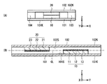
最初に、図1から図3を参照して、本発明における第1の実施の形態としての電流センサの全体構成について説明する。図1は、本実施の形態の電流センサの斜視構成を表す部分破断図であり、図2は、その分解斜視図である。なお、図2では、検出対象電流Imが供給される導体40についても併せて記載し、電流センサとの位置関係を表している。また、図3(A)は矢印IIIに沿って眺めた構成図であり、図3(B)は、第1および第2のモジュール10,20(後述)を含む断面図である。但し、図1および図3では導体40(後述)の図示を省略し、図2および図3ではコイル30(後述)の図示を省略している。
[First Embodiment]
First, the entire configuration of the current sensor as the first embodiment of the present invention will be described with reference to FIGS. 1 to 3. FIG. 1 is a partially cutaway view showing a perspective configuration of a current sensor according to the present embodiment, and FIG. 2 is an exploded perspective view thereof. In FIG. 2, the
この電流センサは第1および第2のモジュール10,20を備えており、例えばY軸に沿って延在する直線部分41を有する導体40(図2参照)の近傍に配置され、導体40に流れる制御信号等の検出対象電流Imの有無や大きさを検出するものである。第1および第2のモジュール10,20は、積層構造を有する磁気抵抗効果(MR;Magneto-Resistive effect)素子5A,5B(後出)をそれぞれ含んでおり、それらの積層面と平行な中心軸CLを回転中心として互いに回転対称な関係にある。すなわち、一方のMR素子(例えばMR素子5A)を中心軸CLを回転中心として180°回転させると、他方のMR素子(MR素子5B)と構造上、等価な関係にある。ここでいう等価な関係とは、そのままの状態で、あるいは、一方が平行移動すれば互いに重なり合う(一致する)構造を有する関係を意味する。なお、中心軸CLは、後述する異方性磁界Hk1,Hk2の方向と平行をなしているとよい。本実施の形態では、中心軸CLをY軸とし、MR素子5A,5Bにおける積層構造の積層面が延在する面内においてY軸と直交する軸をX軸とし、積層構造の積層方向に対応する、X軸およびY軸と直交する軸をZ軸とする。
The current sensor includes first and
導体40は、例えば銅(Cu)などの高導電性の金属材料を用いてめっき法などにより形成された薄膜である。導体40に検出対象電流Imが供給されると、直線部分41の周囲に誘導磁界Hmが発生するようになっている。導体40の端部40S,40Eは、コンタクト層(図示せず)などを介して外部の配線と接続されている。第1および第2のモジュール10,20は誘導磁界Hmを検出するものであり、直線部分41が延在する階層と異なる階層において直線部分41に沿って配置されている。すなわち、第1および第2のモジュール10,20は、積層方向に投影すると直線部分41と重なり合う領域に設けられている。
The
この電流センサでは、検出対象電流Imが端部40Sから端部40Eへ流れると、第1のモジュール10におけるMR素子5Aおよび第2のモジュール20におけるMR素子5Bに対して誘導磁界Hmが+X方向に付与され、検出対象電流Imが端部40Eから端部40Sへ流れると、MR素子5AおよびMR素子5Bに対して誘導磁界Hmが−X方向に付与されることとなる。
In this current sensor, when the detection target current Im flows from the
第1のモジュール10は保持部材としての集積基板101の面101Sに固定されている一方、第2のモジュール20は保持部材としての集積基板102の面102Sに固定されている。集積基板101および集積基板102は、スペーサ103,104を介して面101Sおよび面102Sが対向するように配置されている。集積基板101における面101Sとは反対側の面101K、および集積基板102における面102Sとは反対側の面102Kは、いずれも基準平面であり、導体40の直線部分41と平行に配置される。集積基板101,102およびスペーサ103,104は、例えば酸化アルミニウム(Al2 O3 )によって構成されている。集積基板101,102は図示しない配線パターンや差分検出器AMP(後出)を有するプリント回路基板であり、素子基板11,21と共に後出の図11に示す回路を構成している。
The
電流センサは、さらに、リフレッシュ磁界Hrefを発生させるコイル30を備えている。コイル30は、集積基板101,102の周囲を中心軸CLを中心として巻回している導線である。このコイル30は、電流が流れることにより、異方性磁界Hk1,Hk2の方向(ここでは+Y方向)にリフレッシュ磁界Hrefを発生させ、それをMR素子5A,5Bに印加するものである。リフレッシュ磁界Hrefは、後述する自由層53A,53Bの磁化が飽和する磁界と同等以上の強度を有している。
The current sensor further includes a coil 30 that generates a refresh magnetic field Href. The coil 30 is a conducting wire wound around the
第1のモジュール10は、集積基板101の側から素子基板11とMR素子層12と薄膜コイル層13とを順に積層したものである。集積基板101には、素子基板11が接着層(図示せず)を介して接着されている。同様に、第2のモジュール20は、集積基板102の側から素子基板21とMR素子層22と薄膜コイル層23とを順に積層したものである。集積基板102には、素子基板21が接着層(図示せず)を介して接着されている。
In the
ここで図4および図5を参照して、第1のモジュール10の構成について詳細に説明する。図4は、第1のモジュール10を拡大して表した分解斜視図であり、図5は、図4に示したV−V切断線に沿った矢視方向における断面図である。
Here, the configuration of the
MR素子層12は、例えば100μm程度の厚みをなすシリコンウェハなどの素子基板11上に形成された2つの素子パターン50A1,50A2を有するMR素子5Aを、酸化アルミニウム(Al2 O3 )などの絶縁層Z1で覆うようにしたものである。素子パターン50A1,50A2は、磁性層を含む複数の機能膜が積層されたスピンバルブ構造を有し、巨大磁気抵抗効果を発現するものである。素子パターン50A1,50A2は、素子基板11上においてY軸に沿って互いに平行をなすように延在すると共にY軸と直交するX軸に沿って互いに隣在し合うように配設され、連結部55Aおよび連結部56Aによって互いに並列接続されている。なお、素子パターン50A1,50A2についてのさらなる詳細な構造については後述する。
The
薄膜コイル層13は、MR素子層12の上に形成された薄膜コイル61Aを、Al2 O3などの絶縁層Z2で覆うようにしたものである。薄膜コイル61Aは、薄膜コイル層13の膜面内(XY平面内)において巻回するように構成された薄膜パターンであり、素子パターン50A1,50A2のそれぞれと対応してY軸に沿って延在する巻線体部分62A,63Aを含んでいる。薄膜コイル61Aは、例えば銅(Cu)などの高導電性の金属材料からなり、補償電流Id(後出)が供給されることで補償電流ラインC(後出)の一部として機能するものである。
The thin
薄膜コイル層13の上には電極膜71A〜74Aが設けられており、このうち、電極膜73Aがコンタクトホール(図示せず)を介して連結部55Aと接続され、電極膜74Aがコンタクトホール57A(図5参照)を介して連結部56Aと接続されている。素子パターン50A1,50A2は、スパッタリング法などを用いて例えば0.8μmの厚みを有するように形成される。薄膜コイル61Aにおける一方の端部64Aはコンタクトホール(図示せず)を介して電極膜71Aと接続されており、他方の端部65Aはコンタクトホール(図示せず)を介して電極膜72Aと接続されている。なお、−Y方向へ検出対象電流Imが流れる場合、第1のモジュール10では、補償電流Idが端部65Aから端部64Aへ向かって流れるようになっている。
第2のモジュール20は、第1のモジュール10とほぼ同様の構成を有している。すなわち、図6および図7に示したように、素子基板21、MR素子層22および薄膜コイル層23は、素子基板11、MR素子層12および薄膜コイル層13とそれぞれ対応した構成となっている。図6は、第2のモジュール20を拡大して表した分解斜視図であり、図7は、図6に示したVII−VII切断線に沿った矢視方向における断面図である。MR素子層22において、MR素子5Aに対応するMR素子5Bは、素子パターン50A1,50A2に対応する素子パターン50B1,50B2を有している。素子パターン50B1,50B2は、連結部55Bおよび連結部56Bによって並列接続されている。また、薄膜コイル層23において、薄膜コイル61Aに相当する薄膜コイル61Bは、素子パターン50B1,50B2のそれぞれと対応してY軸に沿って延在する巻線体部分62B,63Bを含んでおり、薄膜コイル61Aと同様に補償電流Idが供給されることで補償電流ラインCの一部として機能するものである。さらに、薄膜コイル層23の上には電極膜71B,72B,73B,74Bが設けられており、このうち、電極膜73Bがコンタクトホール(図示せず)を介して連結部55Bと接続され、電極膜74Bがコンタクトホール56B(図5参照)を介して連結部56Bと接続されている。薄膜コイル61Bにおける一方の端部64Bはコンタクトホール(図示せず)を介して電極膜71Bと接続されており、他方の端部65Bはコンタクトホール(図示せず)を介して電極膜72Bと接続されている。−Y方向へ検出対象電流Imが流れる場合、第2のモジュール20では、補償電流Idが端部64Bから端部65Bへ向かって流れるように接続される。
The
第2のモジュール20では、以下に説明するように、素子パターン50B1,50B2における磁化J51Aの向きが、第1のモジュール10の素子パターン50A1,50A2における磁化J51Bの向きと異なっている。
In the
図8(A)は、図4および図5に示した素子パターン50A1,50A2を拡大した分解斜視図であり、図9(A)は、図6および図7に示した素子パターン50B1,50B2を拡大した分解斜視図である。素子パターン50A1,50A2は、例えば素子基板11の側から、誘導磁界Hmをはじめとする外部磁界に応じて方向が変化する磁化J53Aを有する自由層53Aと、特定の磁化方向を発現しない非磁性の中間層52Aと、一定方向に固着された磁化J51Aを有する固着層51Aとが順に積層されたものである。同様に、素子パターン50B1,50B2は、例えば素子基板21の側から、誘導磁界Hmをはじめとする外部磁界に応じて方向が変化する磁化J53Bを有する自由層53Bと、特定の磁化方向を発現しない非磁性の中間層52Bと、一定方向に固着された磁化J51Bを有する固着層51Bとが順に積層されたものである。
8A is an exploded perspective view enlarging the element patterns 50A1 and 50A2 shown in FIGS. 4 and 5, and FIG. 9A shows the element patterns 50B1 and 50B2 shown in FIGS. It is the disassembled perspective view which expanded. The element patterns 50A1 and 50A2 include, for example, a free layer 53A having a magnetization J53A whose direction changes according to an external magnetic field such as an induction magnetic field Hm and a nonmagnetic non-magnetic material that does not express a specific magnetization direction from the
自由層53A,53Bは、いずれも+Y方向の異方性磁界Hk1,Hk2を発現している。ここでの異方性磁界Hk1,Hk2とは、自由層53A,53Bの結晶構造に起因する異方性磁界成分や、自由層53A,53Bの形状に起因する異方性磁界成分を含む全ての異方性磁界を意味するものである。本実施の形態では、異方性磁界Hk1,Hk2が中心軸CL(Y軸)と平行をなしている。固着層51A,51Bの磁化J51A,J51Bの方向は、図1にも示したように、中心軸CLと直交する直交軸PLからわずかに傾いている。詳細には、磁化J51Aの方向は、+X方向から+Y方向へ角度β1だけ傾いた方向であり、磁化J51Bの方向は、−X方向から+Y方向へ角度β2だけ傾いた方向である。角度β1および角度β2は、互いに等しいことが望ましい。磁化J51A,J51Bの方向と異方性磁界Hk1,Hk2の方向との相対角度は、いずれも0°より大きく90°未満である。
The free layers 53A and 53B both express the anisotropic magnetic fields Hk1 and Hk2 in the + Y direction. The anisotropic magnetic fields Hk1 and Hk2 here include all anisotropic magnetic field components resulting from the crystal structure of the free layers 53A and 53B and all anisotropic magnetic field components resulting from the shapes of the free layers 53A and 53B. It means an anisotropic magnetic field. In the present embodiment, the anisotropic magnetic fields Hk1 and Hk2 are parallel to the central axis CL (Y axis). As shown in FIG. 1, the directions of the magnetizations J51A and J51B of the fixed
図8(B),図9(B)に、固着層51A,51Bの詳細な構成を示す。固着層51A,51Bは、中間層52A,52Bの側から磁化固定膜54A,54Bと反強磁性膜55A,55Bと保護膜56A,56Bとが順に積層されたものである。磁化固定膜54A,54Bはコバルト(Co)やコバルト鉄合金(CoFe)などの強磁性材料からなり、この磁化固定膜54A,54Bの示す磁化方向が固着層51A,51B全体としての磁化J51A,J51Bの方向となる。一方、反強磁性膜55A,55Bは、白金マンガン合金(PtMn)やイリジウムマンガン合金(IrMn)などの反強磁性材料により構成されている。反強磁性膜55A,55Bは、ある一方向のスピン磁気モーメントと、それとは逆方向のスピン磁気モーメントとが完全に打ち消し合った状態にあり、磁化固定膜54A,54Bの磁化方向を固定するように作用している。また、保護膜56A,56Bは、タンタル(Ta)やハフニウム(Hf)などの化学的に安定な非磁性材料からなり、磁化固定膜54A,54Bや反強磁性膜55A,55Bなどを保護するものである。さらに、自由層53A,53Bは、ニッケル鉄合金(NiFe)などの軟磁性材料により構成されており、中間層52A,52Bは、例えば銅や金(Au)などの高導電性の非磁性材料により構成されている。
FIG. 8B and FIG. 9B show detailed structures of the fixing
既に述べたように、MR素子5Aを構成する素子パターン50A1,50A2と、MR素子5Bを構成する素子パターン50B1,50B2とは、中心軸CLを回転中心として互いに回転対称な関係にある。そのうえ、素子パターン50A1,50A2と、素子パターン50B1,50B2とは、その積層面に沿った仮想の共通平面を含む同一の階層に位置している(図3(B)参照)。ここでいう「同一の階層」とは、各素子パターン50A1,50A2,50B1,50B2の少なくとも一部が、厚み方向において互いに等しい高さ位置にあることを意味する。すなわち、各素子パターン50A1,50A2,50B1,50B2をXY平面内において平行移動すると、少なくともそれらの一部が互いに重なり合う位置関係にある。特に、素子パターン50A1,50A2における自由層53Aと、素子パターン50B1,50B2における自由層53Bとが、仮想の共通平面を含むように互いに等しい高さ位置に存在することが望ましい。
As already described, the element patterns 50A1 and 50A2 constituting the
ここで、図8(A),図9(A)は、誘導磁界Hmをはじめとする含む外部磁界が付与されていない無負荷状態を示している。この場合、MR素子5Aにおける磁化のベクトルとMR素子5Bにおける磁界のベクトルとは、中心軸CLを回転の中心として互いに回転対称な関係となっている。また、自由層53Aの磁化J53Aは、固着層51Aおよび自由層53Aの間に生ずる交換結合磁界Hin1と、自由層53Aの異方性磁界Hk1との合成磁界H1の方向を向いている(図10(A))。同様に、自由層53Bの磁化J53Bは、固着層51Bおよび自由層53Bの間に生ずる交換結合磁界Hin2と、自由層53Bの異方性磁界Hk2との合成磁界H2の方向を向いている(図10(B))。一方、固着層51A,51Bの磁化J51A,J51Bは、異方性磁界Hk1,Hk2と0°よりも大きく90°未満の相対角度をなす方向を向いており、例えば合成磁界H1,H2とそれぞれ角度α1,α2をなしている。角度α1,α2は、誘導磁界Hmの有無にかかわらず、いずれも90°であることが望ましい。そのような構成とすることで、MR素子5A,5Bが最大の出力を発現するからである。交換結合磁界Hin1,Hin2は、それぞれ磁化J51A,J51Bと正反対のベクトルを有している。素子パターン50A1,50A2における磁化J51A、異方性磁界Hk1および交換結合磁界Hin1は、それぞれ素子パターン50B1,50B2における磁化J51B、異方性磁界Hk2および交換結合磁界Hin2と等しいことが望ましい。なお、図10(A),図10(B)は、素子パターン50A1,50A2および素子パターン50B1,50B2における磁化の向きおよび大きさと、磁界の向きおよび大きさとを説明するための説明図である。
Here, FIGS. 8A and 9A show a no-load state in which an external magnetic field including the induction magnetic field Hm is not applied. In this case, the magnetization vector in the
素子パターン50A1,50A2に対し、例えば図10(A)に示した誘導磁界Hmが+X方向に印加されると、自由層53Aの磁化J53Aは合成磁界H1と誘導磁界Hmとの合成ベクトルV1の方向へ向きを変える。このとき、磁化J51Aと磁化J53Aとの角度は角度α1よりも小さくなるので、MR素子5Aの抵抗値R1は減少する。一方、素子パターン50B1,50B2に対しても図10(B)に示したように図10(A)と同方向(+X方向)の誘導磁界Hmが印加されるので、自由層53Bの磁化J53Bは合成磁界H2と誘導磁界Hmとの合成ベクトルV2の方向へ向きを変える。このとき、磁化J51Bと磁化J53Bとの角度は角度α2よりも大きくなるので、MR素子5Bの抵抗値R2は増大する。このように電流センサ1では、誘導磁界Hmの印加に伴い、MR素子5Aの抵抗値R1と、MR素子5Bの抵抗値R2とが互いに逆向きの変化を示すように構成されている。
For example, when the induced magnetic field Hm shown in FIG. 10A is applied to the element patterns 50A1 and 50A2 in the + X direction, the magnetization J53A of the free layer 53A is in the direction of the combined vector V1 of the combined magnetic field H1 and the induced magnetic field Hm. Change direction. At this time, since the angle between the magnetization J51A and the magnetization J53A is smaller than the angle α1, the resistance value R1 of the
次に、本実施の形態の電流センサの回路構成について説明する。図11は、電流センサの回路構成を表す概略図である。図11では、Y軸に沿って延在する直線部分41を含む導体40についても併せて示す。MR素子5A,5Bは、直線部分41に沿って配置されている。図11では、MR素子5A,5Bをそれぞれ抵抗体として表している。ここでは、検出対象電流Imが端部40Sから端部40Eへ向かって流れることにより、MR素子5A,5Bに対して+X方向の誘導磁界Hmが印加される様子を表している。
Next, a circuit configuration of the current sensor according to the present embodiment will be described. FIG. 11 is a schematic diagram illustrating a circuit configuration of the current sensor. FIG. 11 also shows the
第1のモジュール10は、MR素子5Aのほか、素子基板11上に形成された定電流源CG1(図1では図示せず)を有している。一方、第2のモジュール20は、MR素子5Bのほか、素子基板21上に形成された定電流源CG2(図1では図示せず)を有している。これらの定電流源CG1,CG2は、MR素子5A,5Bと共に図11のような回路を構成している。MR素子5AおよびMR素子5Bの一端同士(例えば電極膜73Aおよび電極膜73B)は第1の接続点P11において接続され、定電流源CG1および定電流源CG2の一端同士は第2の接続点P12において接続されている。第1の接続点P11は最終的に接地されており、第2の接続点P12には電源Vccが接続されている。さらに、MR素子5Aの他端(第1の接続点P11とは反対側となる電極膜74A)は、第3の接続点P13において定電流源CG1の他端(第2の接続点P12とは反対側となる端部)と接続されており、MR素子5Bの他端(第1の接続点P11とは反対側となる電極膜74A)は、第4の接続点P14において定電流源CG2の他端(第2の接続点P12とは反対側となる端部)と接続されている。ここで、定電流源CG1はMR素子5Aに対して定電流I1を供給し、定電流源CG2はMR素子5Bに対して定電流I2を供給するようになっている。
In addition to the
さらに、この電流センサは差分検出器AMPを有しており、その入力側には第3の接続点P13および第4の接続点P14がそれぞれ接続されている。差分検出器AMPの出力側には、直列接続された薄膜コイル61Aと薄膜コイル61Bとを含む1本の補償電流ラインCが接続されている。この差分検出器AMPは、第1の接続点P11と第2の接続点P12との間に電圧が印加されたときの第3の接続点P13と第4の接続点P14との間の電位差(MR素子5A,5Bのそれぞれに生ずる電圧降下の差分)を検出し、補償電流ラインCに補償電流Idを供給するものである。補償電流ラインCにおける差分検出器AMPと反対側の端部は、抵抗体RLを介して接地されている。抵抗体RLにおける差分検出器AMPの側には、補償電流検出手段Sが接続点T1において接続されている。ここでは、補償電流ラインCを補償電流Idが流れることにより、薄膜コイル61Aの巻線体部分62A,63Aおよび薄膜コイル61Bの巻線体部分62B,63Bにおいて誘導磁界Hmと逆方向の補償磁界Hdが発生するように構成されている。すなわち、補償磁界Hdが−X方向に発生し、誘導磁界Hmを打ち消す方向に作用するようになっている。
Further, this current sensor has a difference detector AMP, and a third connection point P13 and a fourth connection point P14 are connected to the input side thereof. One compensation current line C including a
この作用について、図11に加えて図12を参照して詳細に説明する。図12は、図5および図7に示した断面構成の要部を拡大したものであり、電流の流れる方向と、その電流によって生ずる磁界の方向との関係について模式的に表している。ここでは図示しない導体40に対して−Y方向へ(紙面手前から奥へ)向かうように検出対象電流Imが供給されると、MR素子5A,5Bに対しては+X方向(紙面左方向)の誘導磁界Hmが印加されることとなる。このとき、補償電流Idは、各素子パターン50A1,50A2に対応する巻線体部分62A,63Aの中をそれぞれ+Y方向へ(紙面奥から手前へ)向かうように流れると共に、各素子パターン50B1,50B2にそれぞれ対応する巻線体部分62B,63Bの中をそれぞれ−Y方向へ向かうように流れるように構成されている。したがって、右ねじの法則により、巻線体部分62A,63Aの周囲には紙面上、反時計回りの補償磁界Hdが生じ、一方の巻線体部分62B,63Bの周囲には紙面上、時計回りの補償磁界Hdが生じるので、結果として、各素子パターン50A1,50A2,50B1,50B2に対しては−X方向(紙面右方向)への補償磁界Hd(すなわち、誘導磁界Hmとは反対向きの補償磁界Hd)が付与されることとなる。
This operation will be described in detail with reference to FIG. 12 in addition to FIG. FIG. 12 is an enlarged view of a main part of the cross-sectional configuration shown in FIGS. 5 and 7, and schematically shows the relationship between the direction of current flow and the direction of the magnetic field generated by the current. Here, when the detection target current Im is supplied to the conductor 40 (not shown) in the −Y direction (from the front side to the back side), the
次に、この電流センサの製造方法について説明する。 Next, a method for manufacturing this current sensor will be described.
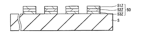
まず、シリコンウェハなどの基体Sの表面に複数のMR素子を一括して形成する。具体的には、まず、図13に示したように、NiFeなどの軟磁性材料からなる自由層53Zと、銅などの非磁性導電材料からなる中間層52Zと、自由層53Zよりも大きな保磁力を有する材料(例えばCoFe)からなる固着層51Zとを基体Sの上に順に積層して積層膜50Zを形成する。この際、全体に亘って一定方向の磁界を印加しながら自由層53Zを成膜することによりその異方性磁界Hkの方向を設定する。積層膜50Zを形成したのち、図14に示したように、その積層膜50Zをフォトリソグラフィ法などによってパターニングすることで、自由層53、中間層52および固着層51からなる所定の寸法形状をなす複数の素子パターン50をそれぞれ基体S上の所定位置に形成する。固着層51については異方性磁界Hkと異なる方向となるように磁化の固着化(規則化)を一括して行う(図示せず)。具体的には、例えば、異方性磁界Hkと異なる方向に(0°より大きく90°未満の相対角度をなすように)1.6kA/m以上160kA/m以下の強さを有する磁界を印加しつつ、250℃以上400℃以下の温度で4時間程度のアニール処理を施すことにより磁化の方向を一括して設定する。この規則化処理によって、外部磁界が零である初期状態での固着層51の磁化J51と自由層53の磁化J53との角度が決まる。そののち、図15に示したように、所定の数(ここでは2つ)の素子パターン50の両端を連結する連結部55,56をそれぞれ形成することにより、複数のMR素子5を得る。図15は、基体Sに形成されたMR素子5の平面構成を表す上面図である。こののち、複数のMR素子5の全体を絶縁層によって覆うことでMR素子層を形成したのち、各MR素子に対応する位置にめっき法などにより薄膜コイルを複数形成し、さらに全体を他の絶縁層によって覆うようにする。
First, a plurality of MR elements are collectively formed on the surface of a substrate S such as a silicon wafer. Specifically, first, as shown in FIG. 13, a
次いで、MR素子5ごとに基体Sを複数に分割する(切り分ける)ことで、素子基板11上にMR素子層12と薄膜コイル層13とが形成された第1のモジュール10(図4参照)と、素子基板21上にMR素子層22と薄膜コイル層23とが形成された第2のモジュール20(図6参照)とを取り出す。ところで、磁化J51と磁化J53との相対的な角度については、同一の基体上に形成されたMR素子同士であっても、若干のばらつきを有することとなる。しかしながら、その角度は、より近い領域に形成されたMR素子同士であれば比較的小さな誤差となる。よって、この電流センサを作製するにあたっては、可能な限り狭い領域内から選択されたMR素子を組み合わせることが望ましい。得られた第1および第2のモジュール10,20を、それぞれ集積基板101,102に貼り付けたのち、集積基板101,102上において定電流源CG1,CG2の形成や配線をおこなう。こののち、自由層53A,53Bの異方性磁界Hk1,Hk2の方向と平行な中心軸CLを回転中心として互いに回転対称な位置となるように、第1のモジュール10が固定された集積基板101と第2のモジュール20が固定された集積基板102とを、スペーサ103,104を介して貼り付ける。こうすることで、誘導磁界Hmに応じて抵抗値R1,R2が互いに逆方向の変化を示すようになる。また、集積基板101と集積基板102とを貼り付ける際には各素子パターンが同一の階層となるようにする。
Next, the first module 10 (see FIG. 4) in which the
最後に、一体化された集積基板101,102の周囲を巻回するようにコイル30を設ける。例えば、銅からなる極細線(φ30μm程度)を巻き付けることでコイル30を形成する。これにより、本実施の形態の電流センサが完成する。
Finally, the coil 30 is provided so as to wind around the integrated
このように構成された電流センサを使用し、誘導磁界Hmに基づいて検出対象電流Imを検出する方法について以下に説明する。 A method for detecting the detection target current Im based on the induced magnetic field Hm using the current sensor configured as described above will be described below.
以下、図11を参照して、検出対象電流Imによって形成される誘導磁界Hmを測定する方法について説明する。 Hereinafter, a method for measuring the induced magnetic field Hm formed by the detection target current Im will be described with reference to FIG.
誘導磁界Hmを検出する準備段階として、まず、コイル30にリフレッシュ電流を流すことにより、自由層53A,53Bの磁化が飽和する磁界と同等以上の大きさを有するリフレッシュ磁界Href(図10)を、MR素子5A,5Bの各々に対して異方性磁界Hk1,Hk2の方向に沿って一時的に印加する。こうすることで、自由層53A,53Bにおける磁化J53A,J53Bの方向を初期状態にリセットすることができる。すなわち、磁化J53A,J53Bの方向を同一方向(異方性磁界Hk1,Hk2の方向)に一旦揃えることができる。この結果、MR素子5A,5Bのヒステリシス現象に伴う検出誤差を回避することができる。さらに、異方性磁界Hk1,Hk2の方向に沿ってリフレッシュ磁界Hrefを一時的に印加することで自由層53A,53Bの結晶磁気異方性が安定化するので(その結果、異方性磁界Hk1,Hk2も安定化するので)、電流センサ1の出力が高いレベルで安定する。
As a preparatory stage for detecting the induction magnetic field Hm, first, a refresh magnetic field Href (FIG. 10) having a magnitude equal to or greater than the magnetic field at which the magnetizations of the free layers 53A and 53B are saturated by flowing a refresh current through the coil 30. A temporary application is applied to each of the
図11において、第1の接続点P11と第2の接続点P12との間に所定の電圧を印加した際の定電流源CG1,CG2からの定電流をそれぞれI1,I2とし、MR素子5A,5Bの抵抗値をそれぞれR1,R2とする。誘導磁界Hmが印加されていない場合、第3の接続点P13における電位V1は、
V1=I1×R1
であり、第4の接続点P14における電位V2は、
V2=I2×R2
となる。よって、第3の接続点P13と第4の接続点P14との間の電位差は、
V0=V1−V2
=I1×R1−I2×R2 …(1)
In FIG. 11, constant currents from the constant current sources CG1 and CG2 when a predetermined voltage is applied between the first connection point P11 and the second connection point P12 are I1 and I2, respectively, and
V1 = I1 × R1
And the potential V2 at the fourth connection point P14 is
V2 = I2 × R2
It becomes. Therefore, the potential difference between the third connection point P13 and the fourth connection point P14 is
V0 = V1-V2
= I1 * R1-I2 * R2 (1)
ここで、定電流I1と定電流I2とが互いに等しい(すなわちI1=I2=I0である)場合には、式(1)は、
V0=I0×(R1−R2) …(2)
となる。
Here, when the constant current I1 and the constant current I2 are equal to each other (that is, I1 = I2 = I0), the expression (1) is
V0 = I0 × (R1-R2) (2)
It becomes.
この回路では、誘導磁界Hmが印加されたときに、電位差V0を測定することにより抵抗変化量が得られる。例えば誘導磁界Hmが印加されたときに、抵抗値R1,R2がそれぞれ変化量ΔR1,ΔR2だけ増加したとすると、式(2)は、
V0=V1−V2
=I0×(R1−R2)
=I0×{(R1+ΔR1)−(R2+ΔR2)} …(3)
となる。
In this circuit, when the induction magnetic field Hm is applied, the resistance change amount is obtained by measuring the potential difference V0. For example, when the induction magnetic field Hm is applied, if the resistance values R1 and R2 increase by the change amounts ΔR1 and ΔR2, respectively, the equation (2) is
V0 = V1-V2
= I0 × (R1-R2)
= I0 × {(R1 + ΔR1) − (R2 + ΔR2)} (3)
It becomes.
本実施の形態では、MR素子5A,5Bにおける各素子パターン50A1,50A2,50B1,50B2が、導体40の直線部分41が延在する階層とは異なる同一の階層に位置しているので、素子パターン50A1,50A2,50B1,50B2のそれぞれと直線部分41との距離は互いにほぼ等しい関係にある。このため、各素子パターン50A1,50A2,50B1,50B2に対してほぼ等しい強度の誘導磁界Hmが付与される。したがって、MR素子5A,5Bは、より正確な変化量ΔR1,ΔR2を示すこととなる。
In the present embodiment, the element patterns 50A1, 50A2, 50B1, and 50B2 in the
すでに述べたように、MR素子5A,5Bは誘導磁界Hmによって各々の抵抗値R1,R2が互いに逆方向の変化を示すように配置されていることから、変化量ΔR1と変化量ΔR2とは互いの正負が逆の符号となる。したがって、式(3)において、誘導磁界Hmが印加される前の抵抗値R1および抵抗値R2は互いに打ち消し合う一方で、変化量ΔR1および変化量ΔR2はそのまま維持される。
As described above, since the
仮に、第1および第2のMR素子11A,11Bが全く同一の特性を有するとした場合、すなわち、
R1=R2=R
かつ
ΔR1=−ΔR2=ΔR
であると仮定した場合、式(3)は、
V0=I0×(R1+ΔR1−R2−ΔR2)
=I0×(R+ΔR−R+ΔR)
=I0×(2×ΔR) …(4)
となる。したがって、外部磁界と抵抗変化量との関係が既知であるMR素子5A,5Bを用いるようにすれば、誘導磁界Hmの大きさを測定することができる。式(4)で表される電位差V0は、合成ベクトルV1,V2と、磁化J51A,J51Bとのなす角度によって決まるものである。
If the first and second MR elements 11A and 11B have exactly the same characteristics, that is,
R1 = R2 = R
And ΔR1 = −ΔR2 = ΔR
Assuming that
V0 = I0 × (R1 + ΔR1-R2-ΔR2)
= I0 × (R + ΔR−R + ΔR)
= I0 × (2 × ΔR) (4)
It becomes. Therefore, the magnitude of the induced magnetic field Hm can be measured by using the
ところで、磁化J51Aと合成磁界H1との角度α1と、磁化J51Bと合成磁界H2との角度α2とが一致していなければ、検出対象磁界Hmを測定する前段階である初期状態においてオフセット出力が生じる(式(2)においてV0=0とならない)こととなる。検出対象磁界Hmが印加されていない無負荷状態であっても、MR素子5Aの抵抗値R1とMR素子5Bの抵抗値R2との差分が零とならないからである。
By the way, if the angle α1 between the magnetization J51A and the combined magnetic field H1 and the angle α2 between the magnetization J51B and the combined magnetic field H2 do not coincide with each other, an offset output is generated in an initial state that is a stage before measuring the detection target magnetic field Hm. (V0 = 0 is not satisfied in the expression (2)). This is because the difference between the resistance value R1 of the
本実施の形態では、MR素子5A,5Bは、異方性磁界Hk1の方向と異方性磁界Hk2の方向とが互いに一致しているうえ、異方性磁界Hk1,Hk2と平行な中心軸CLを回転中心として互いに回転対称な関係を有している。このため、角度α1および角度α2が実質的に同等である。さらに、MR素子5A,5Bは一括形成されたものであるので、実質的に同等の性能を有している。よって、オフセット出力は極めて小さなものとなる。
In the present embodiment, the
さらに、この電流センサでは、第3の接続点P13において検出される電位V1と第4の接続点P14において検出される電位V2とが差分検出器AMPに供給されて、その差分(電位差V0)が零となるような補償電流Idが出力される。差分検出器AMPからの補償電流Idは補償電流ラインCに供給され、MR素子5A,5Bの近傍を所定の方向へ流れることにより誘導磁界Hmとは逆方向の補償磁界Hdを発生させる。この補償磁界Hdは、回路中の接続抵抗のばらつきやMR素子5A,5Bの相互間における特性のばらつき、温度分布の偏り、あるいは外部からの妨害磁界などに起因する誤差分をキャンセルするように作用するので、結果として誘導磁界Hmのみに比例した大きさに近づくこととなる。したがって、補償電流検出手段Sにおいて、出力電圧Voutを測定し、既知の抵抗体RLとの関係から補償電流Idを算出することにより、誘導磁界Hmをより正確に求めることができ、ひいては検出対象電流Imの大きさを高精度に推定することができる。
Further, in this current sensor, the potential V1 detected at the third connection point P13 and the potential V2 detected at the fourth connection point P14 are supplied to the difference detector AMP, and the difference (potential difference V0) is obtained. A compensation current Id that is zero is output. The compensation current Id from the difference detector AMP is supplied to the compensation current line C and flows in the predetermined direction in the vicinity of the
以上説明したように、本実施の形態の電流センサによれば、MR素子5A,5Bにおける各素子パターン50A1,50A2,50B1,50B2を、導体40の直線部分41が延在する階層とは異なる同一の階層に配置するようにしたので、素子パターン50A1,50A2,50B1,50B2のそれぞれと直線部分41との距離を全てほぼ等しくすることができる。このため、各素子パターン50A1,50A2,50B1,50B2に対してほぼ等しい強度の誘導磁界Hmを付与することができるので、MR素子5A,5Bの抵抗値R1,R2は、より正確な変化を示すこととなり、誘導磁界Hm、ひいては検出対象電流Imを高精度に測定することができる。特に、誘導磁界Hmに応じて磁化J53A,J53Bの方向が変化する自由層53A,53Bが、直線部分41に対して互いに対応する高さ位置に存在するようにすれば、MR素子5A,5Bの抵抗値R1,R2の変化がより精密となり、よりいっそう高精度な測定が可能となる。
As described above, according to the current sensor of the present embodiment, each of the element patterns 50A1, 50A2, 50B1, and 50B2 in the
特に、MR素子5A,5Bをそれぞれ素子基板11,21に設け、基準平面としての面101K,102Kをそれぞれ有する集積基板101,102の面101S,102Sにそれら素子基板11,21を固定するようにしたので、面101K,102Kが直線部分41と平行をなすように電流センサを配置することで、素子パターン50A1,50A2,50B1,50B2のそれぞれと直線部分41との距離が等しくなるように簡便に設定することができる。
In particular, the
また、MR素子5A,5Bを、積層面と平行な中心軸CLを中心として互いに回転対称な関係を有するようにしたので、初期状態において、磁化J53Aの方向と磁化J51Aの方向との相対角度α1と、磁化J53Bの方向と磁化J51Bの方向との相対角度α2とが互いに等しくなる。そのうえ、誘導磁界Hmに応じて、MR素子5Aの抵抗値R1とMR素子5Bの抵抗値R2とが互いに逆方向の変化を示すこととなる。その結果、相対角度α1と相対角度α2との誤差に起因するオフセット出力を低減することができ、より高精度に誘導磁界Hmを測定することができる。
In addition, since the
さらに、コイル30を設けるようにしたので、自由層53A,53Bの磁化J53A,J53Bの方向が外部からの不要な磁界(外乱磁界)によって乱された場合であっても、MR素子5A,5Bに対して異方性磁界Hk1,Hk2の方向へリフレッシュ磁界Hrefを印加することができる。これにより、自由層53A,53Bを飽和させ、一旦、磁化J53A,J53Bを一定方向(合成磁界H1,H2の方向)へ揃えることができる。そのうえ、リフレッシュ磁界Hrefを印加することで、異方性磁界Hk1,Hk2の方向も安定化する。したがって、MR素子5A,5Bに対してリフレッシュ磁界Hrefを印加してから誘導磁界Hmを検出するようにすれば、微小な検出対象電流Imであっても、高精度に、かつ安定して測定することができる。
Furthermore, since the coil 30 is provided, even if the directions of the magnetizations J53A and J53B of the free layers 53A and 53B are disturbed by an unnecessary external magnetic field (disturbance magnetic field), the
また、本実施の形態では、同一の基体Sの上に一括形成した複数のMR素子5の全てについて、自由層53の磁化容易軸Hkと固着層51の磁化J51の方向とが互いに異なるように一括して規則化を行ったのち、その基体Sから切り出した第1および第2のモジュール10,20を、中心軸CLを回転中心として互いに回転対称な位置となるように固定するようにしたので、角度α1と角度α2との誤差や、MR素子5A,5Bにおける感度などの性能面での誤差を極めて低く抑えることができる。
In the present embodiment, the easy axis Hk of the free layer 53 and the direction of the magnetization J51 of the pinned layer 51 are different from each other for all of the plurality of
さらに、第3の接続点P13において検出される電位V1と第4の接続点P14において検出される電位V2との差分(MR素子5A,5Bのそれぞれに生ずる電圧降下の差分)V0に基づいた補償電流Idが供給される補償電流ラインCをさらに備え、薄膜コイル61A,61Bによって誘導磁界Hmとは逆方向の補償磁界HdをMR素子5A,5Bに対してそれぞれ付与するようにしたので、MR素子5A,5B同士の特性のばらつきや回路中の接続抵抗のばらつき、あるいは温度分布などに起因した出力電圧Voutの変化をキャンセルすることができ、誘導磁界Hmを、より高感度かつ高精度に検出することができる。
Further, compensation based on the difference V0 between the potential V1 detected at the third connection point P13 and the potential V2 detected at the fourth connection point P14 (difference in voltage drop generated in each of the
[第2の実施の形態]
次に、本発明における第2の実施の形態としての電流センサの構成について説明する。本実施の形態の電流センサは、第1および第2のモジュール10,20の構成が異なることを除き、他は第1の実施の形態の電流センサと同様である。したがって、主に第1の実施の形態の電流センサとの相違点について説明することとし、それ以外の点についての説明は適宜省略する。
[Second Embodiment]
Next, the configuration of a current sensor as a second embodiment of the present invention will be described. The current sensor of the present embodiment is the same as the current sensor of the first embodiment except that the configurations of the first and
図16および図17は、それぞれ、本実施の形態の電流センサにおける第1のモジュール10および第2のモジュール20の斜視構成を表す概略図である。
FIGS. 16 and 17 are schematic views illustrating perspective configurations of the
上記第1の実施の形態の電流センサは、2つのMR素子(MR素子5A,5B)と2つの定電流源(定電流源CG1,CG2)とによって構成されるものである。これに対し、本実施の形態の電流センサは、4つのMR素子(MR素子5A〜5D)によって構成されるものである。
The current sensor of the first embodiment includes two MR elements (
図16に示したように、本実施の形態の第1のモジュール10では、素子基板11の上に設けられたMR素子層12が、MR素子5Aと共にMR素子5Cを含むように構成されている。MR素子5Aは2つの素子パターン50A1,50A2を有し、MR素子5Cは2つの素子パターン50C1,50C2を有している。素子パターン50A1,50A2は、Y軸に沿って互いに平行をなすように延在すると共にX軸に沿って互いに隣在し合うように配設され、連結部55Aおよび連結部56Aによって互いに並列接続されている。同様に、素子パターン50C1,50C2は、Y軸に沿って互いに平行をなすように延在すると共にX軸に沿って互いに隣在し合うように配設され、連結部58Aおよび連結部59Aによって互いに並列接続されている。
As shown in FIG. 16, in the
また、薄膜コイル層13には、MR素子5Aに対応する薄膜コイル61Aと、MR素子5Cに対応する薄膜コイル61CとがそれぞれXY平面内において巻回するように設けられている。詳細には、薄膜コイル61Aは、素子パターン50A1,50A2のそれぞれと対応してY軸に沿って延在する巻線体部分62A,63Aを含んでおり、薄膜コイル61Cは、素子パターン50C1,50C2のそれぞれと対応してY軸に沿って延在する巻線体部分62C,63Cを含んでいる。薄膜コイル61A,61Cは、補償電流Idが供給されることで補償電流ラインCの一部として機能するものである。
The thin
薄膜コイル層13の上には電極膜71A〜78Aが設けられており、このうち、電極膜73A,74A,77A,78Aが、それぞれコンタクトホール(図示せず)を介して連結部55A,56A,58A,59Aと接続されている。また、薄膜コイル61Aにおける一方の端部64Aはコンタクトホール(図示せず)を介して電極膜71Aと接続されており、他方の端部65Aはコンタクトホール(図示せず)を介して電極膜72Aと接続されている。さらに、薄膜コイル61Cにおける端部64C,65Cは、それぞれコンタクトホール(図示せず)を介して電極膜75A,76Aと接続されている。なお、−Y方向へ検出対象電流Imが流れる場合、補償電流Idが、薄膜コイル61Aの内部を端部64Aから端部65Aへ向かって流れ、薄膜コイル61Cの内部を端部65Cから端部64Cへ向かって流れるようになっている。
一方、本実施の形態の第2のモジュール20では、図17に示したように、素子基板21の上に設けられたMR素子層22が、MR素子5Bと共にMR素子5Dを含むように構成されている。また、薄膜コイル層23には、MR素子5Bに対応する薄膜コイル61B共にMR素子5Dに対応する薄膜コイル61DがXY平面内において巻回するように設けられている。MR素子5Bは、素子パターン50B1,50B2に対応する素子パターン50B1,50B2を有しており、それらは連結部55Bおよび連結部56Bによって並列接続されている。一方、MR素子5Dは、素子パターン50D1,50D2に対応する素子パターン50D1,50D2を有しており、それらは連結部58Bおよび連結部59Bによって並列接続されている。また、薄膜コイル61Bは、素子パターン50B1,50B2のそれぞれと対応してY軸に沿って延在する巻線体部分62B,63Bを含んでおり、薄膜コイル61Dは、素子パターン50D1,50D2のそれぞれと対応してY軸に沿って延在する巻線体部分62D,63Dを含んでいる。薄膜コイル61B,61Dは、補償電流Idが供給されることで補償電流ラインCの一部として機能するものである。
On the other hand, in the
さらに、薄膜コイル層23の上には電極膜71B〜78Bが設けられており、このうち、電極膜73B,74B,77B,78Bが、それぞれコンタクトホール(図示せず)を介して連結部55B,56B,58B,59Bと接続されている。また、薄膜コイル61Bにおける一方の端部64Bはコンタクトホール(図示せず)を介して電極膜71Bと接続されており、他方の端部65Bはコンタクトホール(図示せず)を介して電極膜72Bと接続されている。さらに、薄膜コイル61Dにおける端部64D,65Dは、それぞれコンタクトホール(図示せず)を介して電極膜75D,76Dと接続されている。なお、−Y方向へ検出対象電流Imが流れる場合、補償電流Idが、薄膜コイル61Bの内部を端部64Bから端部65Bへ向かって流れ、薄膜コイル61Dの内部を端部65Dから端部64Dへ向かって流れるようになっている。
Furthermore,
本実施の形態のMR素子5A,5Cにおける素子パターン50A1,50A2,50C1,50C2は、上記第1の実施の形態におけるMR素子5Aの素子パターン50A1,50A2と全く同じ構成である。同様に、本実施の形態のMR素子5B,5Dにおける素子パターン50B1,50B2,50D1,50D2は、上記第1の実施の形態におけるMR素子5Bの素子パターン50B1,50B2と全く同じ構成である。すなわち、MR素子5AとMR素子5Cとは互いに等価な関係にあり、MR素子5BとMR素子5Dとは互いに等価な関係にある。したがって、MR素子5A,5Cは、MR素子5B,5Dに対して中心軸CLを中心とした回転対称な関係にある。このような構成により、導体40に検出対象電流Imが流れ、誘導磁界Hmが発生すると、MR素子5AおよびMR素子5Cは互いに同じ挙動を示し、MR素子5BおよびMR素子5Dは、いずれもMR素子5AおよびMR素子5Cと逆の挙動を示すこととなる。
The element patterns 50A1, 50A2, 50C1, and 50C2 in the
ここで、素子パターン50A1,50A2,50C1,50C2は、中心軸から互いに等しい距離に位置することが望ましい。これにより、それらの各素子パターンに対してより均質な誘導磁界Hmを付与することができ、いっそう高精度な測定が可能となるからである。 Here, it is desirable that the element patterns 50A1, 50A2, 50C1, and 50C2 are located at equal distances from the central axis. This is because a more uniform induction magnetic field Hm can be applied to each of these element patterns, and measurement with higher accuracy becomes possible.
この電流センサの製造方法は、上記第1の実施の形態とほぼ同様である。 The manufacturing method of this current sensor is almost the same as that of the first embodiment.
具体的には、まず、シリコンウェハなどの基体の表面に複数のMR素子を一括して形成したのち、MR素子5を2つずつ含むようにその基体を複数に分割する(切り分ける)ことで、図16に示した第1のモジュール10と、図17に示した第2のモジュール20とを取り出す。得られた第1および第2のモジュール10,20を、それぞれ集積基板101,102に貼り付けたのち、中心軸CLを回転中心として互いに回転対称な位置となるように、第1のモジュール10が固定された集積基板101と第2のモジュール20が固定された集積基板102とを、スペーサ103,104を介して貼り付ける。その際、MR素子5A〜5Dの各素子パターンが同一の階層となるようにする。
Specifically, first, a plurality of MR elements are collectively formed on the surface of a substrate such as a silicon wafer, and then the substrate is divided (divided) into a plurality of pieces so as to include two
最後に、一体化された集積基板101,102の周囲を巻回するようにコイル30(図1参照)を設けるなど、所定の工程を経ることで本実施の形態の電流センサが完成する。
Finally, the current sensor of the present embodiment is completed through a predetermined process such as providing the coil 30 (see FIG. 1) so as to wind around the integrated
また、本実施の形態の電流センサの回路構成は図18に示した通りである。ここでは、MR素子5AおよびMR素子5Bの一端同士が第1の接続点P11において接続され、MR素子5CおよびMR素子5Dの一端同士が第2の接続点P12において接続され、MR素子5Aの他端とMR素子5Dの他端とが第3の接続点P13において接続され、MR素子5Bの他端とMR素子5Cの他端とが第4の接続点P14において接続されることにより、ブリッジ回路が構成されている。
The circuit configuration of the current sensor according to the present embodiment is as shown in FIG. Here, one end of
この電流センサでは、誘導磁界Hmの変化に応じて、MR素子5C,5Dが、それぞれ、MR素子5A,5Bと全く同様の挙動を示す。図18において、第1の接続点P11と第2の接続点P12との間に所定の電圧を印加した際の定電流をI0とし、MR素子5A〜5Dの抵抗値をそれぞれR1〜R4とする。誘導磁界Hmが印加されていない場合、第2の接続点P12と第1の接続点P11との電位差Vは、
V=I1×R4+I1×R1=I2×R3+I2×R2
=I1×(R4+R1)=I2×(R3+R2) …(5)
と表すことができる。また、第3の接続点P13における電位V1および第4の接続点P14における電位V2は、それぞれ、
V1=V−V4
=V−I1×R4
V2=V−V3
=V−I2×R3
と表せる。よって、第3の接続点P13と第4の接続点P14との間の電位差V0は、
V0=V1−V2
=(V−I1×R4)−(V−I2×R3)
=I2×R3−I1×R4 …(6)
ここで、(5)式から
V0={R3/(R3+R2)}×V−{R4/(R4+R1)}×V
={R3/(R3+R2)−R4/(R4+R1)}×V …(7)
となる。このブリッジ回路では、誘導磁界Hmが印加されたときに、上記の式(7)で示された第3および第4の接続点P13,P14間の電圧V0を測定することにより、抵抗変化量が得られる。誘導磁界Hmが印加されたときに、抵抗値R1〜R4がそれぞれ変化量ΔR1〜ΔR1だけ増加したとすると、すなわち、抵抗値R1〜R4がそれぞれ、
R1→R1+ΔR1
R2→R2+ΔR2
R3→R3+ΔR3
R4→R4+ΔR4
のように変化したとすると、検出対象磁界Hmを印加したのちは、式(7)より、
V0={(R3+ΔR3)/(R3+ΔR3+R2+ΔR2)−(R4+ΔR4)/(R4+ΔR4+R1+ΔR1)}×V …(8)
となる。すでに述べたように、この電流センサでは、MR素子5A,5Cの抵抗値R1,R3とMR素子5B,5Dの抵抗値R2,R4とが逆方向に変化するので、変化量ΔR3と変化量ΔR2とが打ち消し合うと共に変化量ΔR4と変化量ΔR1とが打ち消し合うこととなる。このため、誘導磁界Hmの印加前後を比較した場合、式(8)の各項における分母の増加はほとんど無い。一方、各項の分子については、変化量ΔR3と変化量ΔR4とは必ず反対の符号を有するので、打ち消し合うことなく増減が現れることとなる。誘導磁界Hmが印加されることにより、MR素子5B,5Dでは、抵抗値は変化量ΔR2,ΔR4(ΔR2,ΔR4<0)の分だけそれぞれ変化する(実質的に低下する)一方で、MR素子5A,5Cでは、抵抗値は変化量ΔR1,ΔR3(ΔR1,ΔR3>0)の分だけそれぞれ変化する(実質的に増加する)からである。
In this current sensor, the
V = I1 * R4 + I1 * R1 = I2 * R3 + I2 * R2
= I1 * (R4 + R1) = I2 * (R3 + R2) (5)
It can be expressed as. The potential V1 at the third connection point P13 and the potential V2 at the fourth connection point P14 are respectively
V1 = V-V4
= V-I1 * R4
V2 = V-V3
= V-I2 * R3
It can be expressed. Therefore, the potential difference V0 between the third connection point P13 and the fourth connection point P14 is
V0 = V1-V2
= (V-I1 * R4)-(V-I2 * R3)
= I2 * R3-I1 * R4 (6)
Here, V0 = {R3 / (R3 + R2)} × V− {R4 / (R4 + R1)} × V from the equation (5).
= {R3 / (R3 + R2) -R4 / (R4 + R1)} * V (7)
It becomes. In this bridge circuit, when the induction magnetic field Hm is applied, the resistance change amount is obtained by measuring the voltage V0 between the third and fourth connection points P13 and P14 expressed by the above equation (7). can get. If the resistance values R1 to R4 are increased by the change amounts ΔR1 to ΔR1 when the induction magnetic field Hm is applied, that is, the resistance values R1 to R4 are respectively
R1 → R1 + ΔR1
R2 → R2 + ΔR2
R3 → R3 + ΔR3
R4 → R4 + ΔR4
After applying the detection target magnetic field Hm, the following equation (7) is obtained:
V0 = {(R3 + ΔR3) / (R3 + ΔR3 + R2 + ΔR2) − (R4 + ΔR4) / (R4 + ΔR4 + R1 + ΔR1)} × V (8)
It becomes. As described above, in this current sensor, the resistance values R1 and R3 of the
本実施の形態では、MR素子5A〜5Dにおける各素子パターン50A1,50A2,50B1,50B2,50C1,50C2,50D1,50D2の全てが、導体40の直線部分41が延在する階層とは異なる同一の階層に位置しているので、各素子パターン50A1,50A2,50B1,50B2,50C1,50C2,50D1,50D2に対してほぼ等しい強度の誘導磁界Hmが付与される。したがって、MR素子5A〜5Dは、より正確な変化量ΔR1,ΔR2,ΔR3,ΔR4を示すこととなる。
In the present embodiment, all of the element patterns 50A1, 50A2, 50B1, 50B2, 50C1, 50C2, 50D1, and 50D2 in the
特に、MR素子5A〜5Dは、一括して形成されたものであり、同一の特性を有するので、すなわち、
R=R1=R2=R3=R4
かつ
ΔR=ΔR1=−ΔR2=ΔR3=−ΔR4
であるので、式(8)は、
V0={(R+ΔR)/(2R)−(R−ΔR)/(2R)}×V
=(ΔR/R)×V
となる。
In particular, the
R = R1 = R2 = R3 = R4
And ΔR = ΔR1 = −ΔR2 = ΔR3 = −ΔR4
Therefore, equation (8) becomes
V0 = {(R + ΔR) / (2R) − (R−ΔR) / (2R)} × V
= (ΔR / R) × V
It becomes.
このように、外部磁界と抵抗変化量との関係が既知であるMR素子5A〜5Dを用いるようにすれば、誘導磁界Hmの大きさを測定することができ、その誘導磁界Hmを派生する検出対象電流Imの大きさを推定することができる。
As described above, if the
さらに、この電流センサでは、上記第1の実施の形態と同様、第3の接続点P13において検出される電位V1と第4の接続点P14において検出される電位V2とが差分検出器AMPに供給されて、その差分(電位差V0)が零となるような補償電流Idが出力される。差分検出器AMPからの補償電流Idは補償電流ラインCに供給され、MR素子5A〜5Dの近傍を所定の方向へ流れることにより誘導磁界Hmとは逆方向の補償磁界Hdを発生するようになっている。
Further, in this current sensor, as in the first embodiment, the potential V1 detected at the third connection point P13 and the potential V2 detected at the fourth connection point P14 are supplied to the difference detector AMP. Thus, a compensation current Id is output so that the difference (potential difference V0) becomes zero. The compensation current Id from the difference detector AMP is supplied to the compensation current line C and flows in the predetermined direction in the vicinity of the
以上説明したように、本実施の形態の電流センサによれば、MR素子5A〜5Dにおける各素子パターン50A1,50A2,50B1,50B2,50C1,50C2,50D1,50D2の全てを、導体40の直線部分41が延在する階層とは異なる同一の階層に配置するようにしたので、誘導磁界Hm、ひいては検出対象電流Imを高精度に測定することができる。特に、自由層が、直線部分41に対して互いに対応する高さ位置に存在するようにすれば、MR素子5A〜5Dの抵抗値R1〜R4の変化がより精密となり、よりいっそう高精度な測定が可能となる。
As described above, according to the current sensor of the present embodiment, all of the element patterns 50A1, 50A2, 50B1, 50B2, 50C1, 50C2, 50D1, and 50D2 in the
以上、いくつかの実施の形態および実施例を挙げて本発明を説明したが、本発明は上記の実施の形態等に限定されず、種々の変形が可能である。例えば上記第1の実施の形態では、異方性磁界Hk1,Hk2の方向が互いに一致するようにMR素子5A,5Bを配置するようにしたが、本発明はこれに限定されるものではない。例えば、図19に示したように、異方性磁界Hk1,Hk2が中心軸CLから外れていてもよい。但し、異方性磁界Hk1の方向や磁化J51Aの方向などが異方性磁界Hk2の方向や磁化J51Bの方向などと中心軸CLを中心として互いに回転対称な関係となっていることが望ましい。この場合、中心軸CLに沿ってリフレッシュ磁界Hrefを印加することで初期状態が得られ、オフセット出力電圧を実質的に零とすることができる。なお、中心軸CLは、異方性磁界Hk1,Hk2、磁化J51A,J51Bおよび交換結合磁界Hin1,Hin2の各ベクトルを全て含む面(通常は積層面)と平行な軸とする。
Although the present invention has been described with reference to some embodiments and examples, the present invention is not limited to the above-described embodiments and the like, and various modifications are possible. For example, in the first embodiment, the
また、上記実施の形態では、保持部材として平板状のプリント回路基板である集積基板101,102を例示して説明したが、これに限定されるものではない。例えば柔軟性を有するフレキシブル基板を保持部材として用いることもできる。また、上記実施の形態では、図1に示したように磁気抵抗効果素子が形成された素子基板を集積基板101,102の中央付近に配置するようにしたが、その配置に限定されるものではない。すなわち、図1では中心軸CLを集積基板101,102のX軸方向の中心位置としたが、中心軸CLがどちらかに偏っていてもよい。また、集積基板101,102には、磁気抵抗効果素子以外の他のデバイスが設けられていてもよい。さらに、磁気抵抗効果素子(MR素子5A〜5D)、補償電流ライン(薄膜コイル61A〜61D)、素子基板(素子基板11,21)および保持部材(集積基板101,102)の相互の寸法比についても各図に示したものに限定されない。
In the above-described embodiment, the
1,2…電流センサ、10…第1のモジュール、11,21…素子基板、12,22…磁気抵抗効果(MR)素子層、13,23…薄膜コイル層、20…第2のモジュール、30…コイル、40…導体、41…直線部分、5A,5B…磁気抵抗効果(MR)素子、50A1,50A2,50B1,50B2…素子パターン、101,102…集積基板、CG1,CG2…定電流源、CL…中心軸、PL…直交軸、β1,β2…角度。
DESCRIPTION OF
Claims (28)
一定方向に固着された磁化方向を有する固着層と、非磁性の中間層と、前記誘導磁界に応じて磁化方向が変化すると共に前記固着層の磁化方向と異なる方向の異方性磁界を発現する自由層とを含む積層構造をそれぞれ有する第1および第2の磁気抵抗効果素子を備え、
前記第1および第2の磁気抵抗効果素子における各積層構造が同一階層に設けられ、
前記第1の磁気抵抗効果素子の抵抗値と前記第2の磁気抵抗効果素子の抵抗値とが前記誘導磁界に応じて互いに逆方向に変化する
ことを特徴とする電流センサ。 A current sensor that is disposed in the vicinity of a conductor that generates an induced magnetic field by supplying a detection target current and detects the detection target current,
A pinned layer having a magnetization direction fixed in a certain direction, a non-magnetic intermediate layer, and an anisotropic magnetic field that changes in direction according to the induction magnetic field and has a direction different from the magnetization direction of the pinned layer. Comprising first and second magnetoresistive elements each having a laminated structure including a free layer,
Each laminated structure in the first and second magnetoresistance effect elements is provided in the same layer,
A current sensor, wherein a resistance value of the first magnetoresistive effect element and a resistance value of the second magnetoresistive effect element change in opposite directions according to the induction magnetic field.
ことを特徴とする請求項1に記載の電流センサ。 The laminated structure of the first magnetoresistive effect element and the laminated structure of the second magnetoresistive effect element are in a rotationally symmetric relationship with each other about a central axis parallel to the laminated surface. The current sensor according to claim 1.
ことを特徴とする請求項2に記載の電流センサ。 The current sensor according to claim 2, wherein the central axis coincides with the direction of the anisotropic magnetic field of the free layer in both the first and second magnetoresistance effect elements.
ことを特徴とする請求項1から請求項3のいずれか1項に記載の電流センサ。 4. The current sensor according to claim 1, wherein all the free layers in the first and second magnetoresistive elements are located in the same layer. 5.
前記保持部材は、前記第1および第2の磁気抵抗効果素子における各積層構造の積層面と平行であり、かつ、外部に露出した基準平面を有する
ことを特徴とする請求項1から請求項4のいずれか1項に記載の電流センサ。 A holding member for holding the first and second magnetoresistive elements;
The holding member has a reference plane that is parallel to the laminated surface of each laminated structure in the first and second magnetoresistive elements and exposed to the outside. The current sensor according to any one of the above.
ことを特徴とする請求項1から請求項4のいずれか1項に記載の電流センサ。 The current sensor according to any one of claims 1 to 4, wherein the first and second magnetoresistive elements are formed on different element substrates, respectively.
前記第2の磁気抵抗効果素子が形成された素子基板は、前記一対の対向面のうちの他方に設けられている
ことを特徴とする請求項6に記載の電流センサ。 The element substrate on which the first magnetoresistive effect element is formed is provided on one of a pair of facing surfaces of a pair of holding members disposed to face each other.
The current sensor according to claim 6, wherein the element substrate on which the second magnetoresistive element is formed is provided on the other of the pair of opposed surfaces.
ことを特徴とする請求項7に記載の電流センサ。 The pair of holding members have a reference plane that is parallel to the laminated surface of each laminated structure of the first and second magnetoresistive elements and exposed to the outside. Current sensor.
前記定電流によって前記第1および第2の磁気抵抗効果素子のそれぞれに生ずる電圧降下の差分を検出する差分検出器と
を備えた
ことを特徴とする請求項1から請求項8のいずれか1項に記載の電流センサ。 First and second constant current sources for supplying constant currents having the same value to each of the first and second magnetoresistive elements;
The differential detector which detects the difference of the voltage drop which arises in each of the said 1st and 2nd magnetoresistive effect element with the said constant current, These are provided. These are any one of Claims 1-8 characterized by the above-mentioned. The current sensor described in 1.
ことを特徴とする請求項9に記載の電流センサ。 When a compensation current corresponding to the difference in voltage drop flows, a compensation magnetic field in a direction opposite to each induction magnetic field applied to the first and second magnetoresistive elements based on the detection target current is generated. The current sensor according to claim 9, further comprising a compensation current line configured to be applied to each of the first and second magnetoresistive elements.
ことを特徴とする請求項1から請求項10のいずれか1項に記載の電流センサ。 11. A bias magnetic field applying means for applying a bias magnetic field along the direction of the anisotropic magnetic field to the first and second magnetoresistive elements is provided. The current sensor according to claim 1.
一定方向に固着された磁化方向を有する固着層と、非磁性の中間層と、前記誘導磁界に応じて磁化方向が変化すると共に前記固着層の磁化方向と異なる方向の異方性磁界を発現する自由層とを含む積層構造をそれぞれ有する第1から第4の磁気抵抗効果素子を備え、
前記第1から第4の磁気抵抗効果素子における各積層構造が同一階層に設けられ、
前記第1の磁気抵抗効果素子の抵抗値と前記第3の磁気抵抗効果素子の抵抗値とが、前記誘導磁界に応じて互いに同方向に変化し、
前記第2および第4の磁気抵抗効果素子の抵抗値が、前記誘導磁界に応じて前記第1および第3の磁気抵抗効果素子の抵抗値と逆方向に変化する
ことを特徴とする電流センサ。 A current sensor that is disposed in the vicinity of a conductor that generates an induced magnetic field by supplying a detection target current and detects the detection target current,
A pinned layer having a magnetization direction fixed in a certain direction, a non-magnetic intermediate layer, and an anisotropic magnetic field that changes in direction according to the induction magnetic field and has a direction different from the magnetization direction of the pinned layer. First to fourth magnetoresistive elements each having a laminated structure including a free layer,
Each laminated structure in the first to fourth magnetoresistance effect elements is provided in the same layer,
The resistance value of the first magnetoresistive effect element and the resistance value of the third magnetoresistive effect element change in the same direction according to the induction magnetic field,
A current sensor, wherein resistance values of the second and fourth magnetoresistance effect elements change in a direction opposite to the resistance values of the first and third magnetoresistance effect elements according to the induction magnetic field.
ことを特徴とする請求項12に記載の電流センサ。 The first to fourth magnetoresistive elements are located at an equal distance from a central axis parallel to the stacked surface of each stacked structure in the first to fourth magnetoresistive elements. 12. The current sensor according to 12.
前記第2および第4の磁気抵抗効果素子の各積層構造は、互いに等価な関係にあり、
前記第1および第3の磁気抵抗効果素子の各積層構造と、前記第2および第4の磁気抵抗効果素子の各積層構造とは、それらの積層面と平行な中心軸を回転中心として互いに回転対称な関係にある
ことを特徴とする請求項12または請求項13に記載の電流センサ。 The stacked structures of the first and third magnetoresistance effect elements are in an equivalent relationship with each other,
The stacked structures of the second and fourth magnetoresistive elements are in an equivalent relationship with each other,
The stacked structures of the first and third magnetoresistive elements and the stacked structures of the second and fourth magnetoresistive elements rotate with each other about a central axis parallel to the stacked surfaces. The current sensor according to claim 12 or 13, wherein the current sensor is in a symmetrical relationship.
ことを特徴とする請求項14に記載の電流センサ。 The current sensor according to claim 14, wherein the central axis coincides with the direction of the anisotropic magnetic field of the free layer in all of the first to fourth magnetoresistive elements.
ことを特徴とする請求項12から請求項15のいずれか1項に記載の電流センサ。 16. The current sensor according to claim 12, wherein all of the free layers in the first to fourth magnetoresistive elements are located in the same layer.
前記保持部材は、前記第1から第4の磁気抵抗効果素子における各積層構造の積層面と平行であり、かつ、外部に露出した基準平面を有する
ことを特徴とする請求項12から請求項16のいずれか1項に記載の電流センサ。 A holding member for holding the first to fourth magnetoresistive elements;
The holding member has a reference plane that is parallel to a laminated surface of each laminated structure of the first to fourth magnetoresistive elements and exposed to the outside. The current sensor according to any one of the above.
ことを特徴とする請求項12から請求項17のいずれか1項に記載の電流センサ。 The first and third magnetoresistive elements are formed on a first element substrate, and the second and fourth magnetoresistive elements are formed on a second element substrate different from the first element substrate. The current sensor according to any one of claims 12 to 17, wherein the current sensor is provided.
前記第2の素子基板は、前記一対の対向面のうちの他方に設けられている
ことを特徴とする請求項18に記載の電流センサ。 The first element substrate is provided on one of a pair of facing surfaces of a pair of holding members disposed to face each other.
The current sensor according to claim 18, wherein the second element substrate is provided on the other of the pair of opposed surfaces.
ことを特徴とする請求項19に記載の電流センサ。 The pair of holding members have a reference plane that is parallel to the laminated surface of each laminated structure of the first to fourth magnetoresistive elements and exposed to the outside. Current sensor.
前記第1の接続点と前記第2の接続点との間に電圧が印加されたときに生ずる前記第3の接続点と前記第4の接続点との間の電位差に応じた補償電流が流れることにより、前記検出対象電流に基づいて前記第1から第4の磁気抵抗効果素子に印加される各誘導磁界とは逆方向の補償磁界を前記第1から第4の磁気抵抗効果素子の各々に付与するように構成された補償電流ラインと
をさらに備えたことを特徴とする請求項12から請求項20のいずれか1項に記載の電流センサ。 One ends of the first and second magnetoresistance effect elements are connected at a first connection point, one ends of the third and fourth magnetoresistance effect elements are connected at a second connection point, and the first The other end of the first magnetoresistive element and the other end of the third magnetoresistive element are connected at a third connection point, and the other end of the second magnetoresistive element and the fourth magnetoresistive element A bridge circuit in which the other end of the effect element is connected at a fourth connection point;
A compensation current corresponding to a potential difference between the third connection point and the fourth connection point that occurs when a voltage is applied between the first connection point and the second connection point flows. Accordingly, a compensation magnetic field in a direction opposite to each induction magnetic field applied to the first to fourth magnetoresistive effect elements based on the detection target current is applied to each of the first to fourth magnetoresistive effect elements. 21. The current sensor according to claim 12, further comprising: a compensation current line configured to be applied.
ことを特徴とする請求項12から請求項21のいずれか1項に記載の電流センサ。 The bias magnetic field applying means for applying a bias magnetic field along the direction of the anisotropic magnetic field to the first to fourth magnetoresistance effect elements is provided. 21. The current sensor according to claim 1.
ことを特徴とする請求項11または請求項22に記載の電流センサ。 The current sensor according to claim 11 or 22, wherein the bias magnetic field applying unit includes a coil.
ことを特徴とする請求項1から請求項23のいずれか1項に記載の電流センサ。 The magnetization direction of the pinned layer is perpendicular to a direction of a combined magnetic field of an exchange coupling magnetic field generated between the pinned layer and the free layer and an anisotropic magnetic field of the free layer. The current sensor according to any one of claims 23.
一の基体上に、一定方向の異方性磁界を発現すると共に前記誘導磁界に応じて磁化方向が変化する第1の強磁性層と、非磁性の中間層と、前記第1の強磁性層よりも大きな保磁力を有する第2の強磁性層とを順に積層してなる積層構造をそれぞれ含む複数の磁気抵抗効果素子を一括して形成する工程と、
前記複数の磁気抵抗効果素子の全てについて、前記異方性磁界の方向と異なる方向となるように前記第2の強磁性層の磁化方向を一括して設定する工程と、
前記基体を前記磁気抵抗効果素子ごとに複数に分割することで、それぞれ一の前記磁気抵抗効果素子が設けられた第1および第2の素子基板を取り出す工程と、
前記第1および第2の素子基板を、前記磁気抵抗効果素子における各積層構造が同一階層に位置し、かつ、前記誘導磁界に応じて前記第1の素子基板における磁気抵抗効果素子の抵抗値と前記第2の素子基板における磁気抵抗効果素子の抵抗値とが互いに逆方向の変化を示すように配置する工程と
を含むことを特徴とする電流センサの製造方法。 A method of manufacturing a current sensor that is disposed in the vicinity of a conductor that generates an induced magnetic field by supplying a detection target current and detects the detection target current,
A first ferromagnetic layer that develops an anisotropic magnetic field in a certain direction and changes a magnetization direction according to the induced magnetic field, a nonmagnetic intermediate layer, and the first ferromagnetic layer on a single substrate. A step of collectively forming a plurality of magnetoresistive elements each including a laminated structure in which a second ferromagnetic layer having a larger coercive force is sequentially laminated;
A step of collectively setting the magnetization direction of the second ferromagnetic layer so as to be different from the direction of the anisotropic magnetic field for all of the plurality of magnetoresistive elements;
Dividing the base into a plurality of magnetoresistive elements, and taking out the first and second element substrates each provided with one magnetoresistive element;
The first and second element substrates are arranged such that each laminated structure in the magnetoresistive effect element is located in the same level, and the resistance value of the magnetoresistive effect element in the first element substrate according to the induction magnetic field And a step of arranging the resistance values of the magnetoresistive effect elements on the second element substrate so as to show changes in opposite directions to each other.
ことを特徴とする請求項25に記載の電流センサの製造方法。 The first and second element substrates are in a rotationally symmetric relationship between the laminated structure of the first element substrate and the laminated structure of the second element substrate with a central axis parallel to the laminated surface as a rotation center. The method of manufacturing a current sensor according to claim 25, wherein the current sensor is arranged so as to be
一の基体上に、一定方向の異方性磁界を発現すると共に前記誘導磁界に応じて磁化方向が変化する第1の強磁性層と、非磁性の中間層と、前記第1の強磁性層よりも大きな保磁力を有する第2の強磁性層とを順に積層してなる積層構造をそれぞれ含む複数の磁気抵抗効果素子を一括して形成する工程と、
前記複数の磁気抵抗効果素子の全てについて、前記異方性磁界の方向と異なる方向となるように前記第2の強磁性層の磁化方向を一括して設定する工程と、
前記基体を複数に分割することで、2つの前記磁気抵抗効果素子を各々含む前記第1および第2の素子モジュールを形成する工程と、
前記第1および第2の素子モジュールを、前記第1から第4の磁気抵抗効果素子における各積層構造が同一階層に位置し、かつ、前記誘導磁界に応じて前記第1の素子モジュールにおける磁気抵抗効果素子の抵抗値と前記第2の素子モジュールにおける磁気抵抗効果素子の抵抗値とが互いに逆方向の変化を示すように配置する工程と
を含むことを特徴とする電流センサの製造方法。 A method of manufacturing a current sensor that is disposed in the vicinity of a conductor that generates an induced magnetic field by supplying a detection target current and detects the detection target current,
A first ferromagnetic layer that develops an anisotropic magnetic field in a certain direction and changes a magnetization direction according to the induced magnetic field, a nonmagnetic intermediate layer, and the first ferromagnetic layer on a single substrate. A step of collectively forming a plurality of magnetoresistive elements each including a laminated structure in which a second ferromagnetic layer having a larger coercive force is sequentially laminated;
A step of collectively setting the magnetization direction of the second ferromagnetic layer so as to be different from the direction of the anisotropic magnetic field for all of the plurality of magnetoresistive elements;
Forming the first and second element modules each including two magnetoresistive elements by dividing the base into a plurality of parts;
In the first and second element modules, the laminated structures of the first to fourth magnetoresistive elements are positioned on the same level, and the magnetoresistive elements of the first element module are responsive to the induced magnetic field. And a step of disposing the resistance value of the effect element and the resistance value of the magnetoresistive effect element in the second element module so as to show changes in opposite directions to each other.
ことを特徴とする請求項27に記載の電流センサの製造方法。 The first and second element modules have a rotationally symmetric relationship between the laminated structure of the first element module and the laminated structure of the second element module with a central axis parallel to the laminated surface as a rotation center. The current sensor manufacturing method according to claim 27, wherein the current sensor is arranged so as to satisfy the following.
Priority Applications (2)
| Application Number | Priority Date | Filing Date | Title |
|---|---|---|---|
| JP2007166576A JP4877095B2 (en) | 2007-06-25 | 2007-06-25 | Current sensor and manufacturing method thereof |
| US12/213,352 US7646196B2 (en) | 2007-06-25 | 2008-06-18 | Current sensor and method of manufacturing current sensor |
Applications Claiming Priority (1)
| Application Number | Priority Date | Filing Date | Title |
|---|---|---|---|
| JP2007166576A JP4877095B2 (en) | 2007-06-25 | 2007-06-25 | Current sensor and manufacturing method thereof |
Publications (3)
| Publication Number | Publication Date |
|---|---|
| JP2009002911A true JP2009002911A (en) | 2009-01-08 |
| JP2009002911A5 JP2009002911A5 (en) | 2010-03-11 |
| JP4877095B2 JP4877095B2 (en) | 2012-02-15 |
Family
ID=40136230
Family Applications (1)
| Application Number | Title | Priority Date | Filing Date |
|---|---|---|---|
| JP2007166576A Active JP4877095B2 (en) | 2007-06-25 | 2007-06-25 | Current sensor and manufacturing method thereof |
Country Status (2)
| Country | Link |
|---|---|
| US (1) | US7646196B2 (en) |
| JP (1) | JP4877095B2 (en) |
Cited By (20)
| Publication number | Priority date | Publication date | Assignee | Title |
|---|---|---|---|---|
| JP2011196798A (en) * | 2010-03-18 | 2011-10-06 | Tdk Corp | Current sensor |
| KR20120040221A (en) * | 2009-07-27 | 2012-04-26 | 후지 덴키 가부시키가이샤 | Non-contact current sensor |
| JPWO2013129276A1 (en) * | 2012-03-02 | 2015-07-30 | Tdk株式会社 | Magnetic sensor element |
| CN105378500A (en) * | 2013-07-19 | 2016-03-02 | 阿莱戈微系统有限责任公司 | Methods and apparatus for magnetic sensor producing a changing magnetic field |
| US9302488B2 (en) | 2009-06-22 | 2016-04-05 | Brother Kogyo Kabushiki Kaisha | Liquid ejecting apparatus |
| JP2017216722A (en) * | 2017-07-24 | 2017-12-07 | Tdk株式会社 | Rectifier and transceiver |
| US10012518B2 (en) | 2016-06-08 | 2018-07-03 | Allegro Microsystems, Llc | Magnetic field sensor for sensing a proximity of an object |
| JP2019148475A (en) * | 2018-02-27 | 2019-09-05 | Tdk株式会社 | Magnetic sensor |
| US10495699B2 (en) | 2013-07-19 | 2019-12-03 | Allegro Microsystems, Llc | Methods and apparatus for magnetic sensor having an integrated coil or magnet to detect a non-ferromagnetic target |
| US10753769B2 (en) | 2014-10-31 | 2020-08-25 | Allegro Microsystems, Llc | Magnetic field sensor providing a movement detector |
| US10823586B2 (en) | 2018-12-26 | 2020-11-03 | Allegro Microsystems, Llc | Magnetic field sensor having unequally spaced magnetic field sensing elements |
| US10837943B2 (en) | 2017-05-26 | 2020-11-17 | Allegro Microsystems, Llc | Magnetic field sensor with error calculation |
| US10996289B2 (en) | 2017-05-26 | 2021-05-04 | Allegro Microsystems, Llc | Coil actuated position sensor with reflected magnetic field |
| US11237020B2 (en) | 2019-11-14 | 2022-02-01 | Allegro Microsystems, Llc | Magnetic field sensor having two rows of magnetic field sensing elements for measuring an angle of rotation of a magnet |
| US11262422B2 (en) | 2020-05-08 | 2022-03-01 | Allegro Microsystems, Llc | Stray-field-immune coil-activated position sensor |
| US11280637B2 (en) | 2019-11-14 | 2022-03-22 | Allegro Microsystems, Llc | High performance magnetic angle sensor |
| US11428755B2 (en) | 2017-05-26 | 2022-08-30 | Allegro Microsystems, Llc | Coil actuated sensor with sensitivity detection |
| US11493361B2 (en) | 2021-02-26 | 2022-11-08 | Allegro Microsystems, Llc | Stray field immune coil-activated sensor |
| US11578997B1 (en) | 2021-08-24 | 2023-02-14 | Allegro Microsystems, Llc | Angle sensor using eddy currents |
| US11680996B2 (en) | 2012-05-10 | 2023-06-20 | Allegro Microsystems, Llc | Methods and apparatus for magnetic sensor having integrated coil |
Families Citing this family (15)
| Publication number | Priority date | Publication date | Assignee | Title |
|---|---|---|---|---|
| JP4361077B2 (en) * | 2006-10-31 | 2009-11-11 | Tdk株式会社 | Magnetic sensor and manufacturing method thereof |
| FR2941534B1 (en) * | 2009-01-26 | 2011-12-23 | Commissariat Energie Atomique | MAGNETIC FIELD SENSOR HAS SUSPENDED STRAIN GAUGE |
| JP5250109B2 (en) * | 2009-06-12 | 2013-07-31 | アルプス・グリーンデバイス株式会社 | Magnetic balanced current sensor |
| WO2010143666A1 (en) * | 2009-06-12 | 2010-12-16 | アルプス・グリーンデバイス株式会社 | Magnetic balance current sensor |
| WO2011081197A1 (en) * | 2009-12-28 | 2011-07-07 | Tdk株式会社 | Magnetic field detecting apparatus and current sensor |
| US8975889B2 (en) * | 2011-01-24 | 2015-03-10 | Infineon Technologies Ag | Current difference sensors, systems and methods |
| FR2979790B1 (en) * | 2011-09-07 | 2013-10-11 | Commissariat Energie Atomique | CURRENT SENSOR |
| US9372242B2 (en) * | 2012-05-11 | 2016-06-21 | Memsic, Inc. | Magnetometer with angled set/reset coil |
| US9529060B2 (en) | 2014-01-09 | 2016-12-27 | Allegro Microsystems, Llc | Magnetoresistance element with improved response to magnetic fields |
| EP3300534B1 (en) | 2015-06-05 | 2020-11-11 | Allegro MicroSystems, LLC | Spin valve magnetoresistance element with improved response to magnetic fields |
| KR101891414B1 (en) * | 2016-12-23 | 2018-08-23 | 전자부품연구원 | Measurement Method and Apparatus for Simultaneous Correction of Sensor Disturbance and Offset |
| US11022661B2 (en) | 2017-05-19 | 2021-06-01 | Allegro Microsystems, Llc | Magnetoresistance element with increased operational range |
| US10620279B2 (en) | 2017-05-19 | 2020-04-14 | Allegro Microsystems, Llc | Magnetoresistance element with increased operational range |
| JP6597820B2 (en) * | 2018-03-12 | 2019-10-30 | Tdk株式会社 | Magnetic sensor and position detection device |
| US11719771B1 (en) | 2022-06-02 | 2023-08-08 | Allegro Microsystems, Llc | Magnetoresistive sensor having seed layer hysteresis suppression |
Citations (7)
| Publication number | Priority date | Publication date | Assignee | Title |
|---|---|---|---|---|
| JPH06294854A (en) * | 1993-01-13 | 1994-10-21 | Lust Electron Syst Gmbh | Sensor chip |
| JPH08226960A (en) * | 1994-11-04 | 1996-09-03 | Internatl Business Mach Corp <Ibm> | Magnetic field sensor and manufacture thereof |
| JP2003066127A (en) * | 2001-08-28 | 2003-03-05 | Alps Electric Co Ltd | Method for assembling magnetic sensor |
| JP2005236134A (en) * | 2004-02-20 | 2005-09-02 | Tdk Corp | Magnetic detecting element, its forming method, magnetic sensor and ammeter |
| JP2006105693A (en) * | 2004-10-01 | 2006-04-20 | Tdk Corp | Current sensor |
| JP2007101252A (en) * | 2005-09-30 | 2007-04-19 | Tdk Corp | Magnetic sensor, its manufacturing method, and current sensor |
| JP2008111801A (en) * | 2006-10-31 | 2008-05-15 | Tdk Corp | Magnetic sensor and its manufacturing method |
Family Cites Families (2)
| Publication number | Priority date | Publication date | Assignee | Title |
|---|---|---|---|---|
| CH670004A5 (en) | 1986-02-10 | 1989-04-28 | Landis & Gyr Ag | |
| US6064552A (en) * | 1997-03-18 | 2000-05-16 | Kabushiki Kaisha Toshiba | Magnetoresistive head having magnetic yoke and giant magnetoresistive element such that a first electrode is formed on the giant magnetoresistive element which in turn is formed on the magnetic yoke which acts as a second electrode |
-
2007
- 2007-06-25 JP JP2007166576A patent/JP4877095B2/en active Active
-
2008
- 2008-06-18 US US12/213,352 patent/US7646196B2/en active Active
Patent Citations (7)
| Publication number | Priority date | Publication date | Assignee | Title |
|---|---|---|---|---|
| JPH06294854A (en) * | 1993-01-13 | 1994-10-21 | Lust Electron Syst Gmbh | Sensor chip |
| JPH08226960A (en) * | 1994-11-04 | 1996-09-03 | Internatl Business Mach Corp <Ibm> | Magnetic field sensor and manufacture thereof |
| JP2003066127A (en) * | 2001-08-28 | 2003-03-05 | Alps Electric Co Ltd | Method for assembling magnetic sensor |
| JP2005236134A (en) * | 2004-02-20 | 2005-09-02 | Tdk Corp | Magnetic detecting element, its forming method, magnetic sensor and ammeter |
| JP2006105693A (en) * | 2004-10-01 | 2006-04-20 | Tdk Corp | Current sensor |
| JP2007101252A (en) * | 2005-09-30 | 2007-04-19 | Tdk Corp | Magnetic sensor, its manufacturing method, and current sensor |
| JP2008111801A (en) * | 2006-10-31 | 2008-05-15 | Tdk Corp | Magnetic sensor and its manufacturing method |
Cited By (29)
| Publication number | Priority date | Publication date | Assignee | Title |
|---|---|---|---|---|
| US9302488B2 (en) | 2009-06-22 | 2016-04-05 | Brother Kogyo Kabushiki Kaisha | Liquid ejecting apparatus |
| US9939466B2 (en) | 2009-07-27 | 2018-04-10 | Iii Holdings 3, Llc | Non-contact current sensor |
| KR20120040221A (en) * | 2009-07-27 | 2012-04-26 | 후지 덴키 가부시키가이샤 | Non-contact current sensor |
| KR101594383B1 (en) | 2009-07-27 | 2016-02-16 | 아이아이아이 홀딩스 3, 엘엘씨 | Non-contact current sensor |
| US8593134B2 (en) | 2010-03-18 | 2013-11-26 | Tdk Corporation | Current sensor |
| JP2011196798A (en) * | 2010-03-18 | 2011-10-06 | Tdk Corp | Current sensor |
| JPWO2013129276A1 (en) * | 2012-03-02 | 2015-07-30 | Tdk株式会社 | Magnetic sensor element |
| US11680996B2 (en) | 2012-05-10 | 2023-06-20 | Allegro Microsystems, Llc | Methods and apparatus for magnetic sensor having integrated coil |
| US10145908B2 (en) | 2013-07-19 | 2018-12-04 | Allegro Microsystems, Llc | Method and apparatus for magnetic sensor producing a changing magnetic field |
| CN105378500A (en) * | 2013-07-19 | 2016-03-02 | 阿莱戈微系统有限责任公司 | Methods and apparatus for magnetic sensor producing a changing magnetic field |
| US10495699B2 (en) | 2013-07-19 | 2019-12-03 | Allegro Microsystems, Llc | Methods and apparatus for magnetic sensor having an integrated coil or magnet to detect a non-ferromagnetic target |
| US10670672B2 (en) | 2013-07-19 | 2020-06-02 | Allegro Microsystems, Llc | Method and apparatus for magnetic sensor producing a changing magnetic field |
| US11313924B2 (en) | 2013-07-19 | 2022-04-26 | Allegro Microsystems, Llc | Method and apparatus for magnetic sensor producing a changing magnetic field |
| US11307054B2 (en) | 2014-10-31 | 2022-04-19 | Allegro Microsystems, Llc | Magnetic field sensor providing a movement detector |
| US10753769B2 (en) | 2014-10-31 | 2020-08-25 | Allegro Microsystems, Llc | Magnetic field sensor providing a movement detector |
| US10012518B2 (en) | 2016-06-08 | 2018-07-03 | Allegro Microsystems, Llc | Magnetic field sensor for sensing a proximity of an object |
| US11768256B2 (en) | 2017-05-26 | 2023-09-26 | Allegro Microsystems, Llc | Coil actuated sensor with sensitivity detection |
| US11428755B2 (en) | 2017-05-26 | 2022-08-30 | Allegro Microsystems, Llc | Coil actuated sensor with sensitivity detection |
| US10837943B2 (en) | 2017-05-26 | 2020-11-17 | Allegro Microsystems, Llc | Magnetic field sensor with error calculation |
| US10996289B2 (en) | 2017-05-26 | 2021-05-04 | Allegro Microsystems, Llc | Coil actuated position sensor with reflected magnetic field |
| JP2017216722A (en) * | 2017-07-24 | 2017-12-07 | Tdk株式会社 | Rectifier and transceiver |
| WO2019167598A1 (en) * | 2018-02-27 | 2019-09-06 | Tdk株式会社 | Magnetic sensor |
| JP2019148475A (en) * | 2018-02-27 | 2019-09-05 | Tdk株式会社 | Magnetic sensor |
| US10823586B2 (en) | 2018-12-26 | 2020-11-03 | Allegro Microsystems, Llc | Magnetic field sensor having unequally spaced magnetic field sensing elements |
| US11280637B2 (en) | 2019-11-14 | 2022-03-22 | Allegro Microsystems, Llc | High performance magnetic angle sensor |
| US11237020B2 (en) | 2019-11-14 | 2022-02-01 | Allegro Microsystems, Llc | Magnetic field sensor having two rows of magnetic field sensing elements for measuring an angle of rotation of a magnet |
| US11262422B2 (en) | 2020-05-08 | 2022-03-01 | Allegro Microsystems, Llc | Stray-field-immune coil-activated position sensor |
| US11493361B2 (en) | 2021-02-26 | 2022-11-08 | Allegro Microsystems, Llc | Stray field immune coil-activated sensor |
| US11578997B1 (en) | 2021-08-24 | 2023-02-14 | Allegro Microsystems, Llc | Angle sensor using eddy currents |
Also Published As
| Publication number | Publication date |
|---|---|
| US20080316655A1 (en) | 2008-12-25 |
| JP4877095B2 (en) | 2012-02-15 |
| US7646196B2 (en) | 2010-01-12 |
Similar Documents
| Publication | Publication Date | Title |
|---|---|---|
| JP4877095B2 (en) | Current sensor and manufacturing method thereof | |
| JP4361077B2 (en) | Magnetic sensor and manufacturing method thereof | |
| JP4930627B2 (en) | Magnetic sensor | |
| JP4105142B2 (en) | Current sensor | |
| JP6130775B2 (en) | Current sensor | |
| JP4105147B2 (en) | Current sensor | |
| JP5250108B2 (en) | Magnetic balanced current sensor | |
| JP5012939B2 (en) | Current sensor | |
| US7737678B2 (en) | Magnetic sensor and current sensor | |
| JP4360998B2 (en) | Current sensor | |
| JP5888402B2 (en) | Magnetic sensor element | |
| JP2011064653A (en) | Magnetic sensor and method of manufacturing the same | |
| JP2011047929A (en) | Magnetic sensor | |
| WO2011111536A1 (en) | Magnetic-balance current sensor | |
| JP7324331B2 (en) | Magnetic detector | |
| WO2011111537A1 (en) | Current sensor | |
| JP5447616B2 (en) | Manufacturing method of magnetic sensor | |
| JP2011027633A (en) | Magnetic sensor and manufacturing method thereof | |
| JP7232647B2 (en) | Magnetic detector | |
| JP2007298329A (en) | Angle sensor |
Legal Events
| Date | Code | Title | Description |
|---|---|---|---|
| A621 | Written request for application examination |
Free format text: JAPANESE INTERMEDIATE CODE: A621 Effective date: 20100118 |
|
| A521 | Request for written amendment filed |
Free format text: JAPANESE INTERMEDIATE CODE: A523 Effective date: 20100125 |
|
| A977 | Report on retrieval |
Free format text: JAPANESE INTERMEDIATE CODE: A971007 Effective date: 20110707 |
|
| A131 | Notification of reasons for refusal |
Free format text: JAPANESE INTERMEDIATE CODE: A131 Effective date: 20110712 |
|
| A521 | Request for written amendment filed |
Free format text: JAPANESE INTERMEDIATE CODE: A523 Effective date: 20110909 |
|
| TRDD | Decision of grant or rejection written | ||
| A01 | Written decision to grant a patent or to grant a registration (utility model) |
Free format text: JAPANESE INTERMEDIATE CODE: A01 Effective date: 20111101 |
|
| A01 | Written decision to grant a patent or to grant a registration (utility model) |
Free format text: JAPANESE INTERMEDIATE CODE: A01 |
|
| A61 | First payment of annual fees (during grant procedure) |
Free format text: JAPANESE INTERMEDIATE CODE: A61 Effective date: 20111114 |
|
| R150 | Certificate of patent or registration of utility model |
Ref document number: 4877095 Country of ref document: JP Free format text: JAPANESE INTERMEDIATE CODE: R150 Free format text: JAPANESE INTERMEDIATE CODE: R150 |
|
| FPAY | Renewal fee payment (event date is renewal date of database) |
Free format text: PAYMENT UNTIL: 20141209 Year of fee payment: 3 |