JP2022098977A - Semiconductor device - Google Patents
Semiconductor device Download PDFInfo
- Publication number
- JP2022098977A JP2022098977A JP2020212680A JP2020212680A JP2022098977A JP 2022098977 A JP2022098977 A JP 2022098977A JP 2020212680 A JP2020212680 A JP 2020212680A JP 2020212680 A JP2020212680 A JP 2020212680A JP 2022098977 A JP2022098977 A JP 2022098977A
- Authority
- JP
- Japan
- Prior art keywords
- terminal
- solder
- region
- electrode
- main surface
- Prior art date
- Legal status (The legal status is an assumption and is not a legal conclusion. Google has not performed a legal analysis and makes no representation as to the accuracy of the status listed.)
- Pending
Links
- 239000004065 semiconductor Substances 0.000 title claims abstract description 54
- 229910000679 solder Inorganic materials 0.000 claims abstract description 52
- 239000000758 substrate Substances 0.000 claims abstract description 35
- 229910052751 metal Inorganic materials 0.000 claims abstract description 9
- 239000002184 metal Substances 0.000 claims abstract description 9
- 238000009736 wetting Methods 0.000 claims abstract description 9
- 230000002265 prevention Effects 0.000 claims description 2
- 230000005684 electric field Effects 0.000 abstract description 10
- 239000010408 film Substances 0.000 description 80
- 230000001681 protective effect Effects 0.000 description 59
- 230000002093 peripheral effect Effects 0.000 description 31
- PXHVJJICTQNCMI-UHFFFAOYSA-N Nickel Chemical compound [Ni] PXHVJJICTQNCMI-UHFFFAOYSA-N 0.000 description 4
- 230000004048 modification Effects 0.000 description 4
- 238000012986 modification Methods 0.000 description 4
- RYGMFSIKBFXOCR-UHFFFAOYSA-N Copper Chemical compound [Cu] RYGMFSIKBFXOCR-UHFFFAOYSA-N 0.000 description 3
- 229910052802 copper Inorganic materials 0.000 description 3
- 239000010949 copper Substances 0.000 description 3
- 239000000463 material Substances 0.000 description 3
- 239000004642 Polyimide Substances 0.000 description 2
- 229910052759 nickel Inorganic materials 0.000 description 2
- 229920001721 polyimide Polymers 0.000 description 2
- 239000002344 surface layer Substances 0.000 description 2
- 239000010409 thin film Substances 0.000 description 2
- 229910052782 aluminium Inorganic materials 0.000 description 1
- XAGFODPZIPBFFR-UHFFFAOYSA-N aluminium Chemical compound [Al] XAGFODPZIPBFFR-UHFFFAOYSA-N 0.000 description 1
- 238000013459 approach Methods 0.000 description 1
- 239000000470 constituent Substances 0.000 description 1
- 230000000694 effects Effects 0.000 description 1
- 238000000034 method Methods 0.000 description 1
- 238000007747 plating Methods 0.000 description 1
- 229910052710 silicon Inorganic materials 0.000 description 1
- 239000010703 silicon Substances 0.000 description 1
- HBMJWWWQQXIZIP-UHFFFAOYSA-N silicon carbide Chemical compound [Si+]#[C-] HBMJWWWQQXIZIP-UHFFFAOYSA-N 0.000 description 1
- 229910010271 silicon carbide Inorganic materials 0.000 description 1
- 238000005476 soldering Methods 0.000 description 1
- 238000000427 thin-film deposition Methods 0.000 description 1
- 238000011179 visual inspection Methods 0.000 description 1
Images


Classifications
-
- H—ELECTRICITY
- H01—ELECTRIC ELEMENTS
- H01L—SEMICONDUCTOR DEVICES NOT COVERED BY CLASS H10
- H01L23/00—Details of semiconductor or other solid state devices
- H01L23/34—Arrangements for cooling, heating, ventilating or temperature compensation ; Temperature sensing arrangements
- H01L23/36—Selection of materials, or shaping, to facilitate cooling or heating, e.g. heatsinks
-
- H—ELECTRICITY
- H01—ELECTRIC ELEMENTS
- H01L—SEMICONDUCTOR DEVICES NOT COVERED BY CLASS H10
- H01L23/00—Details of semiconductor or other solid state devices
- H01L23/52—Arrangements for conducting electric current within the device in operation from one component to another, i.e. interconnections, e.g. wires, lead frames
- H01L23/522—Arrangements for conducting electric current within the device in operation from one component to another, i.e. interconnections, e.g. wires, lead frames including external interconnections consisting of a multilayer structure of conductive and insulating layers inseparably formed on the semiconductor body
- H01L23/5228—Resistive arrangements or effects of, or between, wiring layers
-
- H—ELECTRICITY
- H01—ELECTRIC ELEMENTS
- H01L—SEMICONDUCTOR DEVICES NOT COVERED BY CLASS H10
- H01L25/00—Assemblies consisting of a plurality of individual semiconductor or other solid state devices ; Multistep manufacturing processes thereof
- H01L25/03—Assemblies consisting of a plurality of individual semiconductor or other solid state devices ; Multistep manufacturing processes thereof all the devices being of a type provided for in the same subgroup of groups H01L27/00 - H01L33/00, or in a single subclass of H10K, H10N, e.g. assemblies of rectifier diodes
- H01L25/04—Assemblies consisting of a plurality of individual semiconductor or other solid state devices ; Multistep manufacturing processes thereof all the devices being of a type provided for in the same subgroup of groups H01L27/00 - H01L33/00, or in a single subclass of H10K, H10N, e.g. assemblies of rectifier diodes the devices not having separate containers
- H01L25/07—Assemblies consisting of a plurality of individual semiconductor or other solid state devices ; Multistep manufacturing processes thereof all the devices being of a type provided for in the same subgroup of groups H01L27/00 - H01L33/00, or in a single subclass of H10K, H10N, e.g. assemblies of rectifier diodes the devices not having separate containers the devices being of a type provided for in group H01L29/00
-
- H—ELECTRICITY
- H01—ELECTRIC ELEMENTS
- H01L—SEMICONDUCTOR DEVICES NOT COVERED BY CLASS H10
- H01L25/00—Assemblies consisting of a plurality of individual semiconductor or other solid state devices ; Multistep manufacturing processes thereof
- H01L25/18—Assemblies consisting of a plurality of individual semiconductor or other solid state devices ; Multistep manufacturing processes thereof the devices being of types provided for in two or more different subgroups of the same main group of groups H01L27/00 - H01L33/00, or in a single subclass of H10K, H10N
-
- H—ELECTRICITY
- H01—ELECTRIC ELEMENTS
- H01L—SEMICONDUCTOR DEVICES NOT COVERED BY CLASS H10
- H01L29/00—Semiconductor devices adapted for rectifying, amplifying, oscillating or switching, or capacitors or resistors with at least one potential-jump barrier or surface barrier, e.g. PN junction depletion layer or carrier concentration layer; Details of semiconductor bodies or of electrodes thereof ; Multistep manufacturing processes therefor
- H01L29/02—Semiconductor bodies ; Multistep manufacturing processes therefor
- H01L29/06—Semiconductor bodies ; Multistep manufacturing processes therefor characterised by their shape; characterised by the shapes, relative sizes, or dispositions of the semiconductor regions ; characterised by the concentration or distribution of impurities within semiconductor regions
-
- H—ELECTRICITY
- H01—ELECTRIC ELEMENTS
- H01L—SEMICONDUCTOR DEVICES NOT COVERED BY CLASS H10
- H01L29/00—Semiconductor devices adapted for rectifying, amplifying, oscillating or switching, or capacitors or resistors with at least one potential-jump barrier or surface barrier, e.g. PN junction depletion layer or carrier concentration layer; Details of semiconductor bodies or of electrodes thereof ; Multistep manufacturing processes therefor
- H01L29/66—Types of semiconductor device ; Multistep manufacturing processes therefor
- H01L29/66007—Multistep manufacturing processes
- H01L29/66075—Multistep manufacturing processes of devices having semiconductor bodies comprising group 14 or group 13/15 materials
- H01L29/66227—Multistep manufacturing processes of devices having semiconductor bodies comprising group 14 or group 13/15 materials the devices being controllable only by the electric current supplied or the electric potential applied, to an electrode which does not carry the current to be rectified, amplified or switched, e.g. three-terminal devices
- H01L29/66409—Unipolar field-effect transistors
- H01L29/66477—Unipolar field-effect transistors with an insulated gate, i.e. MISFET
-
- H—ELECTRICITY
- H01—ELECTRIC ELEMENTS
- H01L—SEMICONDUCTOR DEVICES NOT COVERED BY CLASS H10
- H01L29/00—Semiconductor devices adapted for rectifying, amplifying, oscillating or switching, or capacitors or resistors with at least one potential-jump barrier or surface barrier, e.g. PN junction depletion layer or carrier concentration layer; Details of semiconductor bodies or of electrodes thereof ; Multistep manufacturing processes therefor
- H01L29/66—Types of semiconductor device ; Multistep manufacturing processes therefor
- H01L29/68—Types of semiconductor device ; Multistep manufacturing processes therefor controllable by only the electric current supplied, or only the electric potential applied, to an electrode which does not carry the current to be rectified, amplified or switched
- H01L29/70—Bipolar devices
- H01L29/72—Transistor-type devices, i.e. able to continuously respond to applied control signals
- H01L29/739—Transistor-type devices, i.e. able to continuously respond to applied control signals controlled by field-effect, e.g. bipolar static induction transistors [BSIT]
- H01L29/7393—Insulated gate bipolar mode transistors, i.e. IGBT; IGT; COMFET
- H01L29/7395—Vertical transistors, e.g. vertical IGBT
-
- H—ELECTRICITY
- H01—ELECTRIC ELEMENTS
- H01L—SEMICONDUCTOR DEVICES NOT COVERED BY CLASS H10
- H01L29/00—Semiconductor devices adapted for rectifying, amplifying, oscillating or switching, or capacitors or resistors with at least one potential-jump barrier or surface barrier, e.g. PN junction depletion layer or carrier concentration layer; Details of semiconductor bodies or of electrodes thereof ; Multistep manufacturing processes therefor
- H01L29/66—Types of semiconductor device ; Multistep manufacturing processes therefor
- H01L29/68—Types of semiconductor device ; Multistep manufacturing processes therefor controllable by only the electric current supplied, or only the electric potential applied, to an electrode which does not carry the current to be rectified, amplified or switched
- H01L29/76—Unipolar devices, e.g. field effect transistors
- H01L29/772—Field effect transistors
- H01L29/78—Field effect transistors with field effect produced by an insulated gate
-
- H—ELECTRICITY
- H01—ELECTRIC ELEMENTS
- H01L—SEMICONDUCTOR DEVICES NOT COVERED BY CLASS H10
- H01L29/00—Semiconductor devices adapted for rectifying, amplifying, oscillating or switching, or capacitors or resistors with at least one potential-jump barrier or surface barrier, e.g. PN junction depletion layer or carrier concentration layer; Details of semiconductor bodies or of electrodes thereof ; Multistep manufacturing processes therefor
- H01L29/02—Semiconductor bodies ; Multistep manufacturing processes therefor
- H01L29/06—Semiconductor bodies ; Multistep manufacturing processes therefor characterised by their shape; characterised by the shapes, relative sizes, or dispositions of the semiconductor regions ; characterised by the concentration or distribution of impurities within semiconductor regions
- H01L29/0603—Semiconductor bodies ; Multistep manufacturing processes therefor characterised by their shape; characterised by the shapes, relative sizes, or dispositions of the semiconductor regions ; characterised by the concentration or distribution of impurities within semiconductor regions characterised by particular constructional design considerations, e.g. for preventing surface leakage, for controlling electric field concentration or for internal isolations regions
- H01L29/0607—Semiconductor bodies ; Multistep manufacturing processes therefor characterised by their shape; characterised by the shapes, relative sizes, or dispositions of the semiconductor regions ; characterised by the concentration or distribution of impurities within semiconductor regions characterised by particular constructional design considerations, e.g. for preventing surface leakage, for controlling electric field concentration or for internal isolations regions for preventing surface leakage or controlling electric field concentration
- H01L29/0611—Semiconductor bodies ; Multistep manufacturing processes therefor characterised by their shape; characterised by the shapes, relative sizes, or dispositions of the semiconductor regions ; characterised by the concentration or distribution of impurities within semiconductor regions characterised by particular constructional design considerations, e.g. for preventing surface leakage, for controlling electric field concentration or for internal isolations regions for preventing surface leakage or controlling electric field concentration for increasing or controlling the breakdown voltage of reverse biased devices
- H01L29/0615—Semiconductor bodies ; Multistep manufacturing processes therefor characterised by their shape; characterised by the shapes, relative sizes, or dispositions of the semiconductor regions ; characterised by the concentration or distribution of impurities within semiconductor regions characterised by particular constructional design considerations, e.g. for preventing surface leakage, for controlling electric field concentration or for internal isolations regions for preventing surface leakage or controlling electric field concentration for increasing or controlling the breakdown voltage of reverse biased devices by the doping profile or the shape or the arrangement of the PN junction, or with supplementary regions, e.g. junction termination extension [JTE]
- H01L29/0619—Semiconductor bodies ; Multistep manufacturing processes therefor characterised by their shape; characterised by the shapes, relative sizes, or dispositions of the semiconductor regions ; characterised by the concentration or distribution of impurities within semiconductor regions characterised by particular constructional design considerations, e.g. for preventing surface leakage, for controlling electric field concentration or for internal isolations regions for preventing surface leakage or controlling electric field concentration for increasing or controlling the breakdown voltage of reverse biased devices by the doping profile or the shape or the arrangement of the PN junction, or with supplementary regions, e.g. junction termination extension [JTE] with a supplementary region doped oppositely to or in rectifying contact with the semiconductor containing or contacting region, e.g. guard rings with PN or Schottky junction
-
- H—ELECTRICITY
- H01—ELECTRIC ELEMENTS
- H01L—SEMICONDUCTOR DEVICES NOT COVERED BY CLASS H10
- H01L29/00—Semiconductor devices adapted for rectifying, amplifying, oscillating or switching, or capacitors or resistors with at least one potential-jump barrier or surface barrier, e.g. PN junction depletion layer or carrier concentration layer; Details of semiconductor bodies or of electrodes thereof ; Multistep manufacturing processes therefor
- H01L29/40—Electrodes ; Multistep manufacturing processes therefor
- H01L29/41—Electrodes ; Multistep manufacturing processes therefor characterised by their shape, relative sizes or dispositions
- H01L29/417—Electrodes ; Multistep manufacturing processes therefor characterised by their shape, relative sizes or dispositions carrying the current to be rectified, amplified or switched
Abstract
Description
本明細書に記載の開示は、半導体基板を備える半導体装置に関するものである。 The disclosure described herein relates to a semiconductor device comprising a semiconductor substrate.
特許文献1には、一面に電極と保護膜の形成された半導体基板と、電極に設けられたはんだと、はんだに設けられたターミナルと、を備える半導体装置が記載されている。 Patent Document 1 describes a semiconductor device including a semiconductor substrate having an electrode and a protective film formed on one surface thereof, a solder provided on the electrode, and a terminal provided on the solder.
保護膜は、電極とはんだを囲むようにして半導体基板の一面に形成されている。半導体基板における保護膜の形成された部位にはガードリングなどの耐圧構造部が形成されている。 The protective film is formed on one surface of the semiconductor substrate so as to surround the electrodes and the solder. A pressure-resistant structure such as a guard ring is formed on the portion of the semiconductor substrate on which the protective film is formed.
ターミナルが耐圧構造部側にずれると、ターミナルと耐圧構造部の間の電界分布が変化する。耐圧構造部に電界集中が起こる虞がある。 When the terminal is displaced toward the withstand voltage structure, the electric field distribution between the terminal and the withstand voltage structure changes. There is a risk that electric field concentration will occur in the pressure-resistant structure.
そこで本開示の目的は、耐圧構造部に電界集中が起こることの抑制された半導体装置を提供することである。 Therefore, an object of the present disclosure is to provide a semiconductor device in which electric field concentration is suppressed in the withstand voltage structure portion.
本開示の一態様による半導体装置は、
主面(200a)と、主面の第1領域(281)に設けられた電極(210)と、主面の第1領域とは異なる第2領域(283)に設けられた耐圧構造部(230)と、主面の第1領域と第2領域の間の第3領域(282)に設けられた介在部(270)と、を備える半導体基板(200)と、
電極に設けられたはんだ(310)と、
はんだに設けられ、はんだに濡れない不濡れ部(420)を備える金属製のターミナル(400)と、を有し、
介在部は電極よりもはんだに濡れにくく、
介在部における主面に沿い、なおかつ、第1領域と第2領域が並ぶ、並び方向の長さが、不濡れ部の並び方向の長さよりも長くなっている。
The semiconductor device according to one aspect of the present disclosure is
The pressure resistant structure portion (230) provided in the main surface (200a), the electrodes (210) provided in the first region (281) of the main surface, and the second region (283) different from the first region of the main surface. ), And a semiconductor substrate (200) including an interposition portion (270) provided in a third region (282) between the first region and the second region of the main surface.
Solder (310) provided on the electrode and
It has a metal terminal (400), which is provided on the solder and has a non-wetting portion (420) that does not get wet with the solder.
Intervening parts are less likely to get wet with solder than electrodes
The length in the alignment direction along the main surface of the intervening portion and where the first region and the second region are aligned is longer than the length in the alignment direction of the non-wetting portion.
これによれば耐圧構造部に電界集中が起こることが抑制される。 As a result, it is possible to suppress the occurrence of electric field concentration in the withstand voltage structure portion.
なお、上記の括弧内の参照番号は、後述の実施形態に記載の構成との対応関係を示すものに過ぎず、技術的範囲を何ら制限するものではない。 It should be noted that the reference numbers in parentheses above merely indicate the correspondence with the configurations described in the embodiments described later, and do not limit the technical scope at all.
以下、図面を参照しながら本開示を実施するための複数の形態を説明する。各形態において先行する形態で説明した事項に対応する部分には同一の参照符号を付して重複する説明を省略する場合がある。各形態において構成の一部のみを説明している場合は、構成の他の部分については先行して説明した他の形態を適用することができる。 Hereinafter, a plurality of embodiments for carrying out the present disclosure will be described with reference to the drawings. In each form, the same reference numerals may be given to the parts corresponding to the matters described in the preceding forms, and duplicate explanations may be omitted. When only a part of the configuration is described in each form, other forms described above can be applied to the other parts of the configuration.
また、各実施形態で組み合わせが可能であることを明示している部分同士の組み合わせばかりではなく、特に組み合わせに支障が生じなければ、明示していなくても実施形態同士、実施形態と変形例、および、変形例同士を部分的に組み合せることも可能である。 In addition, not only the combination of the parts that clearly indicate that the combination is possible in each embodiment, but also the embodiments and the modified examples, even if the combination is not specified, if there is no particular problem in the combination. It is also possible to partially combine the modified examples.
(第1実施形態)
以下に、半導体装置100の機械的構成を説明する。それに当たって互いに直交の関係にある3方向をx方向、y方向、および、z方向とする。なお図面においては「方向」の記載を省略して示している。z方向は直交方向に相当する。
(First Embodiment)
The mechanical configuration of the
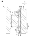
図1に示すように、半導体装置100は、半導体基板200、第1はんだ310、第2はんだ320、第3はんだ330、ターミナル400、第1ヒートシンク500、第2ヒートシンク600、および、不図示の複数の端子を有している。複数の端子とは例えば信号端子、第1主端子、および、第2主端子などである。
As shown in FIG. 1, the
半導体装置100は、三相インバータを構成する6つのアームのうちの1つを構成する所謂1in1パッケージとして知られている。半導体装置100は例えば車両のインバータ回路に組み入れられる。
The
半導体基板200は、シリコン、シリコンカーバイドなどの半導体部材に、絶縁ゲートバイポーラトランジスタ(IGBT)やMOSFETなどのパワートランジスタが形成されて成る。パワートランジスタは、z方向に電流が流れるように所謂縦型構造を成している。
The
半導体基板200は、z方向に厚さの薄い扁平形状を成している。半導体基板200はz方向に離間して並ぶ第1主面200aと第1主面200aの裏側の第2主面200bを有している。第1主面200aが主面に相当する。
The
半導体基板200は第1主面200aと第2主面200bの他に、エミッタ電極210、複数のパッド220、複数の耐圧構造部230、第1保護膜240、第2保護膜250、ダミー電極260、および、コレクタ電極290を有している。
In addition to the first
図1~図4に示すように、半導体基板200の第1主面200aに、エミッタ電極210、複数のパッド220、複数の耐圧構造部230、第1保護膜240、第2保護膜250、および、ダミー電極260が設けられている。半導体基板200の第2主面200bにコレクタ電極290が設けられている。なお、エミッタ電極210は電極に相当する。第1保護膜240は第1構造部に相当する。ダミー電極260は第2構造部に相当する。
As shown in FIGS. 1 to 4, on the first
複数のパッド220は、信号用の電極である。図2に示すように複数のパッド220は、半導体基板200のy方向の端側に設けられている。複数のパッド220は第2保護膜250から露出されている。
The plurality of
複数のパッド220それぞれは、例えば、ゲート電極用、ケルビンエミッタ用、電流センス用、温度センサのアノード電位用、同じく温度センサのカソード電位用などに用いられる。複数のパッド220は、不図示のボンディングワイヤを介して、不図示の複数の信号端子に電気的に接続されている。
Each of the plurality of
ターミナル400は略直方体形状を成すブロック体である。図1に示すように、ターミナル400はz方向に離間して並ぶ第1ターミナル面400aとその裏側の第2ターミナル面400bと第1ターミナル面400aと第2ターミナル面400bを連結する4つの連結ターミナル面400cを有する。
The
ターミナル400は第1はんだ310を介してエミッタ電極210と電気的および機械的に接続されている。ターミナル400は第2はんだ320を介して第2ヒートシンク600と電気的および機械的に接続されている。
The
ターミナル400は半導体基板200と第2ヒートシンク600との熱伝導、電気伝導経路の途中に位置している。そのためターミナル400は熱伝導性及び電気伝導性に優れる例えば銅などの金属部材を用いて形成されている。
The
第1ヒートシンク500は平板形状を成している。第1ヒートシンク500には、不図示の第1主端子が連なっている。第1主端子は半導体基板200のコレクタ電極290と電気的に接続されている。
The
第1ヒートシンク500は、半導体基板200に形成されたパワートランジスタの熱を、半導体基板200の外部に放熱する放熱機能と、コレクタ電極290と第1主端子とを電気的に中継する機能を果たしている。
The
第1ヒートシンク500は第3はんだ330を介して半導体基板200に電気的および機械的に接続されている。第1ヒートシンク500は、ターミナル400同様、熱伝導性および電気伝導性に優れる例えば銅などの金属部材を用いて形成されている。
The
なお、第1主端子は、リードフレームの一部として、第1ヒートシンク500と一体的に形成されていてもよいし、第1ヒートシンク500とは別部材として構成されてもよい。
The first main terminal may be integrally formed with the
第2ヒートシンク600も同様に平板形状を成している。第2ヒートシンク600には、不図示の第2主端子が連なっている。第2主端子は半導体基板200のエミッタ電極210と電気的に接続されている。
The
第2ヒートシンク600は、半導体基板200に形成されたパワートランジスタの熱を、半導体基板200の外部に放熱する放熱機能と、エミッタ電極210と第2主端子とを電気的に中継する機能を果たしている。
The
第2ヒートシンク600は、ターミナル400および第1ヒートシンク500同様、熱伝導性および電気伝導性に優れる例えば銅などの金属部材を用いて形成されている。
Like the terminal 400 and the
なお、第2主端子は、リードフレームの一部として、第2ヒートシンク600と一体的に形成されていてもよいし、第2ヒートシンク600とは別部材として構成されていてもよい。
The second main terminal may be integrally formed with the
<半導体基板>
図3および図4に基づき、半導体基板200の詳細構造について説明する。図示しないが半導体基板200の主面に沿う平面方向の中心から平面方向に所定距離広がるアクティブ領域280の第1主面200a側の表層に、パワートランジスタが設けられている。
<Semiconductor substrate>
The detailed structure of the
言い換えればパワートランジスタが第1主面200aのアクティブ領域280に対応する部位に設けられている。なお、説明を簡便とするために、以下、第1主面200aのアクティブ領域280に対応する部位を、単に第1主面200aのアクティブ領域280と示す。
In other words, the power transistor is provided at the portion corresponding to the
またアクティブ領域280はガードリングなどの耐圧構造部230が複数設けられた耐圧構造領域283にz方向周りの周方向で包囲されている。また耐圧構造領域283の第1主面200a側の表層に複数の耐圧構造部230が設けられている。
Further, the
すなわち複数の耐圧構造部230が第1主面200aの耐圧構造領域283に対応する部位に設けられている。なお、説明を簡便とするために、以下、第1主面200aの耐圧構造領域283に対応する部位を、単に第1主面200aの耐圧構造領域283と示す。
That is, a plurality of pressure-
複数の耐圧構造部230は耐圧構造領域283でx方向に並んでいる。なお、耐圧構造部230はパワートランジスタの耐圧を保持する機能を有していればガードリングでなくてもよい。耐圧構造領域283は第2領域に相当する。
The plurality of pressure-
なお、図面においてはアクティブ領域280と耐圧構造領域283との境界を破線で示している。
In the drawing, the boundary between the
またアクティブ領域280は第1アクティブ領域281と第1アクティブ領域281をz方向周りの周方向で包囲する第2アクティブ領域282から成る。図面においては第1アクティブ領域281と第2アクティブ領域282との境界を一点鎖線で示している。なお、第1アクティブ領域281は第1領域に相当する。第2アクティブ領域282は第3領域に相当する。
Further, the
第2アクティブ領域282は第1アクティブ領域281と耐圧構造領域283が第1主面200aに沿って並ぶ並び方向で第1アクティブ領域281と耐圧構造領域283の間に設けられている。
The second
なお、パワートランジスタは第1アクティブ領域281と第2アクティブ領域282の両方に設けられていなくても良い。パワートランジスタは少なくとも第1アクティブ領域281に設けられていればよい。
The power transistor may not be provided in both the first
以下、説明を簡便とするために、第1主面200aの第1アクティブ領域281に対応する部位を、単に第1主面200aの第1アクティブ領域281と示している。第1主面200aの第2アクティブ領域282に対応する部位を、単に第1主面200aの第2アクティブ領域282と示している。
Hereinafter, for the sake of simplicity, the portion corresponding to the first
<エミッタ電極>
エミッタ電極210は下地電極211と上地電極212を有している。下地電極211が、第1主面200aの第1アクティブ領域281に設けられている。下地電極211が第1アクティブ領域281に設けられたパワートランジスタと電気的に接続されている。
<Emitter electrode>
The
下地電極211は、アルミニウムを主成分とする材料を用いて形成されている。下地電極211の厚みは、たとえば5μmとなっている。
The
下地電極211の第1主面200aから離間した側の部位には、第1はんだ310との接合強度や濡れ性向上などを目的とした上地電極212が形成されている。上地電極212は、たとえばニッケルを主成分とする材料を用いて形成されている。上地電極212の厚みは、5μm~10μm程度となっている。なお、上地電極212として、多層構造を採用することもできる。なお、コレクタ電極290も同様の構造を成している。
A
<第1保護膜>
第1保護膜240はエミッタ電極210よりも第1はんだ310に濡れにくい部材から成る。例えば第1保護膜240はポリイミドやレジストなどである。図1~図4に示すように第1保護膜240はエミッタ電極210を囲む環状形状を成している。
<First protective film>
The first
より具体的に言えば、第1保護膜240がエミッタ電極210をz方向周りの周方向で囲む態様で、第1主面200aの第2アクティブ領域282に設けられている。第1保護膜240はエミッタ電極210と並び方向で隣接している。
More specifically, the first
<ダミー電極>
ダミー電極260はエミッタ電極210と同様の構成を成している。図1~図4に示すようにダミー電極260は第1保護膜240を囲む環状形状を成している。
<Dummy electrode>
The
より具体的に言えば、ダミー電極260が第1保護膜240をz方向周りの周方向で囲む環状形状を成している。ダミー電極260が第1保護膜240をz方向周りの周方向で囲む態様で、第1主面200aの第2アクティブ領域282に設けられている。ダミー電極260は第1保護膜240と並び方向で隣接している。
More specifically, the
また図3および図4に示すように、ダミー電極260はエミッタ電極210と電気的に分離されている。なお、図9に示すようにダミー電極260がエミッタ電極210と電気的に分離されていなくてもよい。その場合ダミー電極260はエミッタ電極210と同電位になっていてもよい。
Further, as shown in FIGS. 3 and 4, the
<第2保護膜>
第2保護膜250はエミッタ電極210よりも第1はんだ310に濡れにくい部材から成る。例えば第2保護膜250はそれぞれポリイミドやレジストなどである。図1~図4に示すように第2保護膜250はダミー電極260を囲む環状形状を成している。
<Second protective film>
The second
より具体的に言えば、第2保護膜250がダミー電極260をz方向周りの周方向で囲む態様で、第1主面200aの耐圧構造領域283に設けられている。第2保護膜250がダミー電極260と並び方向で隣接している。
More specifically, the second
上記したように耐圧構造領域283には複数の耐圧構造部230が設けられている。複数の耐圧構造部230が第2保護膜250によって被覆されている。
As described above, the pressure
<第1保護膜および第2保護膜とダミー電極>
上記したように、第1保護膜240がエミッタ電極210を囲む環状形状を成している。ダミー電極260が第1保護膜240を囲む環状形状を成している。第2保護膜250がダミー電極260を囲む環状形状を成している。ダミー電極260が周方向の全周で、並び方向において第1保護膜240と第2保護膜250の間に設けられている。
<1st protective film, 2nd protective film and dummy electrode>
As described above, the first
ダミー電極260は第1保護膜240および第2保護膜250と組成が異なっている。ダミー電極260は第1保護膜240と第2保護膜250の境界を示す役割を担っている。
The
<半導体基板の電位>
エミッタ電極210の電位がGNDレベルで、コレクタ電極290の電位が略1200Vであるとすると、半導体基板200の各部位における電位は、エミッタ電極210から遠ざかるほどにコレクタ電極290の電位に近付くようになっている。第2アクティブ領域282と耐圧構造領域283を併せた領域における各部位の電位は、エミッタ電極210から遠ざかるほどにコレクタ電極290の電位に近付くようになっている。
<Electric potential of semiconductor substrate>
Assuming that the potential of the
<半導体基板とターミナルとの位置関係>
これまでに説明したようにターミナル400は第1はんだ310を介してエミッタ電極210と電気的および機械的に接続されている。図1~図4に示すようにターミナル400はz方向でエミッタ電極210のすべてと重なっている。またターミナル400のすべてが、エミッタ電極210と第1保護膜240を併せた部位とz方向で重なっている。
<Positional relationship between semiconductor substrate and terminal>
As described above, the terminal 400 is electrically and mechanically connected to the
長さに換言すれば、ターミナル400のx方向の長さが、第1保護膜240におけるエミッタ電極210側で環状形状を成す内面240aのうちのx方向で並ぶ2つの間の距離よりも長くなっている。同様に、ターミナル400のy方向に沿う長さが、第1保護膜240におけるエミッタ電極210側で環状形状を成す内面240aのうちのy方向で並ぶ2つの間の距離よりも長くなっている。
In other words, the length of the terminal 400 in the x direction is longer than the distance between two of the
ターミナル400のx方向の長さが、第1保護膜240におけるダミー電極260側で環状形状を成す外面240bのうちのx方向で並ぶ2つの間の距離も短くなっている。同様にターミナル400のy方向の長さが、第1保護膜240におけるダミー電極260側で環状形状を成す外面240bのうちのy方向で並ぶ2つの間の距離よりも短くなっている。
The length of the terminal 400 in the x direction also shortens the distance between two of the
<第1保護膜とダミー電極を併せた部位とターミナルにおける第1はんだに不濡れの部位との長さ関係>
以下、説明を簡便とするために第1保護膜240とダミー電極260を併せた部位を介在部270とする。図3および図4に示すように第1保護膜240とダミー電極260とが並び方向で並んでいる。介在部270は周方向の全周で並び方向においてエミッタ電極210と第2保護膜250の間に設けられている。
<Length relationship between the part where the first protective film and the dummy electrode are combined and the part that is not wet with the first solder in the terminal>
Hereinafter, for the sake of simplicity, the portion where the first
介在部270とターミナル400における第1はんだ310に不濡れの部位との長さ関係を説明するに当たって、ターミナル400とエミッタ電極210との第1はんだ310を介した接続形態について説明する。
In explaining the length relationship between the intervening
上記したように、第1保護膜240がエミッタ電極210を周方向で囲むように第1主面200aに設けられている。
As described above, the first
そのために第1はんだ310が介在部270から遠ざかるようにして、ターミナル400とエミッタ電極210との間に設けられている。図3および図4に示すように、第1はんだ310が、ターミナル400とエミッタ電極210の間で略錘台形状を成している。
Therefore, the
以下、ターミナル400における第1はんだ310に濡れて半導体基板200に接続される部位をターミナル接続部410と示す。ターミナル400におけるターミナル接続部410の周方向まわりの第1はんだ310の不濡れで半導体基板200に非接続になっている部位をターミナル外周部420と示す。
Hereinafter, the portion of the terminal 400 that gets wet with the
ターミナル接続部410のエミッタ電極210側のターミナル接続面410aが第1はんだ310に濡れて半導体基板200に接続されている。ターミナル外周部420のエミッタ電極210側のターミナル外周面420aが第1はんだ310と不濡れで半導体基板200と非接続になっている。
The
なお、ターミナル接続面410aとターミナル外周面420aとが合わさって第1ターミナル面400aになっている。図面においてはターミナル接続部410とターミナル外周部420の境界を二点鎖線で示す。ターミナル外周部420は不濡れ部に相当する。
The
図3および図4に示すように、ターミナル外周部420のうちのx方向の一端側のx方向の長さが、介在部270のうちのx方向の一端側のx方向の幅よりも短くなっている。ターミナル外周部420のうちのx方向の他端側のx方向の長さが、介在部270のうちのx方向の他端側のx方向の幅よりも短くなっている。
As shown in FIGS. 3 and 4, the length in the x direction of the terminal outer
図示しないが、ターミナル外周部420のうちのy方向の一端側のy方向の長さが、介在部270のうちのy方向の一端側のy方向の幅よりも短くなっている。ターミナル外周部420のうちのy方向の他端側のy方向の長さが、介在部270のうちのy方向の他端側y方向の幅よりも短くなっている。
Although not shown, the length of the outer
ターミナル外周部420の四隅のx方向とy方向それぞれに沿う方向の長さが、介在部270の四隅のx方向とy方向それぞれに沿う方向の幅よりも短くなっている。
The lengths of the four corners of the terminal outer
このように介在部270の並び方向の長さが、ターミナル外周部420の並び方向の長さよりも必ず長くなるように設計されている。図4に示すように、ターミナル400が第1はんだ310上で滑って、耐圧構造領域283側に移動したとしても、介在部270の並び方向の長さが、ターミナル外周部420の並び方向の長さよりも必ず長くなるように設計されている。
As described above, the length of the intervening
ターミナル外周部420の並び方向の長さは、介在部270の並び方向の長さより短くなることが期待される長さに相当している。
The length of the terminal outer
(第2実施形態)
第2実施形態としてターミナル400が第1はんだ310と第2はんだ320にターミナル400より濡れにくい粗化膜340を有する形態を示す。図5に示すように粗化膜340が連結ターミナル面400cとターミナル外周面420aに設けられている。
(Second Embodiment)
As a second embodiment, the terminal 400 has a roughened
粗化膜340はターミナル外周面420aに意図的に設けられていても良いし、意図的でなくてもターミナル外周面420aに設けられていれば良い。例えば、連結ターミナル面400cに粗化膜340が設けられる過程で、ターミナル外周面420aに粗化膜340が設けられていても良い。なお粗化膜340は酸化膜である。粗化膜340は、はんだ防止膜に相当する。
The roughened
粗化膜340は金属を構成材料とする金属薄膜に凹凸形状が形成されて成されたものである。本実施形態の粗化膜340は、ニッケルを主成分としている。金属薄膜は例えばめっき、蒸着により形成されている。
The roughened
上記したように粗化膜340はターミナル400よりも第1はんだ310と第2はんだ320それぞれに濡れにくい部材から成っている。そのために第1はんだ310と第2はんだ320それぞれが連結ターミナル面400cに濡れ拡がりにくくなくなっている。さらに第1はんだ310がターミナル外周面420aに濡れ拡がりにくくなくなっている。
As described above, the roughened
第2実施形態においても、介在部270の並び方向の長さは、ターミナル外周部420の並び方向の長さよりも必ず長くなるように設計されている。
Also in the second embodiment, the length of the intervening
また、図6に示すようにターミナル外周面420aのすべてに粗化膜340が設けられていなくても良い。ターミナル外周面420aに粗化膜340の設けられる部位と粗化膜340の設けられない部位が含まれていても良い。
Further, as shown in FIG. 6, the roughened
また、図7に示すように粗化膜340が連結ターミナル面400cとターミナル外周面420aの両方に設けられていなくても良い。粗化膜340がターミナル外周面420aのみに設けられていても良い。
Further, as shown in FIG. 7, the roughened
(第3実施形態)
さらに、図8に示すように粗化膜340が連結ターミナル面400cとターミナル外周面420aの両方に設けられずに、粗化膜340が連結ターミナル面400cのみに設けられていても良い。
(Third Embodiment)
Further, as shown in FIG. 8, the roughened
第3実施形態においても、介在部270の並び方向の長さは、ターミナル外周部420の並び方向の長さよりも必ず長くなるように設計されている。
Also in the third embodiment, the length of the intervening
(第1変形例)
これまでに説明した第1実施形態~第3実施形態では、ダミー電極260がエミッタ電極210と電気的に分離された形態について説明した。しかしながら図9に示すようにエミッタ電極210の下地電極211とダミー電極260の下地電極211が一体的に連結されることで、ダミー電極260がエミッタ電極210と同電位になっていてもよい。下地電極211の一部が第1保護膜240と第2保護膜250それぞれに被覆されていても良い。
(First modification)
In the first to third embodiments described so far, a mode in which the
(第2変形例)
これまでに説明した第1実施形態~第3実施形態では、介在部270に第1保護膜240とダミー電極260の両方が含まれている形態について説明した。しかしながら図10に示すように介在部270にダミー電極260が含まれていなくても良い。介在部270に第1保護膜240のみが含まれていても良い。下地電極211の一部が第1保護膜240に被覆されていてもよい。第1保護膜240と第2保護膜250とが一体的に連結されていても良い。
(Second modification)
In the first to third embodiments described so far, a mode in which both the first
<作用効果>
これまでに説明したように、介在部270は周方向の全周で並び方向でエミッタ電極210と第2保護膜250の間に設けられている。介在部270の並び方向の長さがターミナル外周部420の並び方向の長さよりも必ず長くなるように設計されている。
<Action effect>
As described above, the intervening
そのために例えば図4に示すように、ターミナル400が第1はんだ310上で滑って、耐圧構造領域283側に移動したとしても、ターミナル400が耐圧構造領域283と必ず並び方向で離間するようになっている。
Therefore, for example, as shown in FIG. 4, even if the terminal 400 slips on the
ターミナル400が耐圧構造領域283側に近付くと、耐圧構造領域283とターミナル400の間の電界分布が変化する。ターミナル400が耐圧構造領域283の近傍まで移動すると、耐圧構造領域283に設けられる耐圧構造部230とターミナル400との間の電界分布が変化する。その際、耐圧構造部230に電界集中が起こりやすくなる。特にターミナル400が耐圧構造部230とz方向で対向すると、耐圧構造部230に電界集中が起こりやすくなる。
When the terminal 400 approaches the withstand
しかしながら第1実施形態~第3実施形態および変形例では上記したようにターミナル400が耐圧構造領域283と必ずx方向で離間するようになっている。ターミナル外周部420の耐圧構造領域283側の端部が第2アクティブ領域282とz方向で対向するようになっている。そのために耐圧構造部230に電界集中が起こることが抑制されやすくなっている。耐圧構造部230の電位の変動が抑制されやすくなっている。それに伴いパワートランジスタの耐圧の変動が抑制されやすくなっている。
However, in the first to third embodiments and the modified examples, the terminal 400 is always separated from the pressure
これまでに説明したようにターミナル外周面420aに粗化膜340が設けられている。上記したように介在部270の並び方向の長さは、ターミナル外周部420の並び方向の長さよりも長くなるように設計される。そのために介在部270の並び方向の長さが規定されやすくなっている。
As described above, the roughened
これまでに説明したようにターミナル400とエミッタ電極210とが第1はんだ310を介して接続されている。ターミナル400がz方向でエミッタ電極210のすべてと重なっている。そのために半導体基板200の熱がターミナル400に放熱されやすくなっている。
As described above, the terminal 400 and the
これまでに説明したようにダミー電極260が周方向の全周において並び方向で第1保護膜240と第2保護膜250の間に設けられている。そのためにターミナル400が第2保護膜250にz方向で対向してるか否かが外観で判別されやすくなっている。外観検査の効率が向上されやすくなっている。
As described above, the
200…半導体基板、200a…第1主面、210…エミッタ電極、230…耐圧構造部、240…第1保護膜、260…ダミー電極、270…介在部、281…第1アクティブ領域、282…第2アクティブ領域、283…耐圧構造領域、310…第1はんだ、340…粗化膜、400…ターミナル、420…ターミナル外周部 200 ... semiconductor substrate, 200a ... first main surface, 210 ... emitter electrode, 230 ... pressure resistant structure part, 240 ... first protective film, 260 ... dummy electrode, 270 ... intervening part, 281 ... first active region, 282 ... 2 active region, 283 ... pressure resistant structure region, 310 ... first solder, 340 ... roughened film, 400 ... terminal, 420 ... terminal outer periphery
Claims (5)
前記電極に設けられたはんだ(310)と、
前記はんだに設けられ、前記はんだに濡れない不濡れ部(420)を備える金属製のターミナル(400)と、を有し、
前記介在部は前記電極よりも前記はんだに濡れにくく、
前記介在部における前記主面に沿い、なおかつ、前記第1領域と前記第2領域が並ぶ、並び方向の長さが、前記不濡れ部の前記並び方向の長さよりも長くなっている半導体装置。
A pressure resistant structure provided in a main surface (200a), an electrode (210) provided in the first region (281) of the main surface, and a second region (283) different from the first region of the main surface. A semiconductor substrate (200) comprising a portion (230) and an intervening portion (270) provided in a third region (282) between the first region and the second region of the main surface.
With the solder (310) provided on the electrode,
It has a metal terminal (400) provided on the solder and provided with a non-wetting portion (420) that does not get wet with the solder.
The intervening portion is less likely to get wet with the solder than the electrode,
A semiconductor device in which the length of the alignment direction along the main surface of the intervening portion and the first region and the second region are aligned is longer than the length of the non-wetting portion in the alignment direction.
前記はんだ防止膜が前記不濡れ部の前記主面側の部位の少なくとも一部に設けられている請求項1に記載の半導体装置。
The terminal has a solder prevention film (340) that is less likely to get wet with the solder than the terminal.
The semiconductor device according to claim 1, wherein the anti-solder film is provided on at least a part of the non-wetting portion on the main surface side.
The semiconductor device according to claim 1 or 2, wherein all of the electrodes overlap with the terminal in an orthogonal direction orthogonal to the main surface.
The intervening portion is less likely to get wet with the solder than the electrode, and is adjacent to the electrode in the alignment direction and extends in the circumferential direction around the orthogonal direction orthogonal to the main surface to form an annular shape with the first structural portion (240). 1. The semiconductor device according to the section.
Priority Applications (4)
| Application Number | Priority Date | Filing Date | Title |
|---|---|---|---|
| JP2020212680A JP2022098977A (en) | 2020-12-22 | 2020-12-22 | Semiconductor device |
| CN202180086142.2A CN116636004A (en) | 2020-12-22 | 2021-11-25 | Semiconductor device with a semiconductor device having a plurality of semiconductor chips |
| PCT/JP2021/043194 WO2022137966A1 (en) | 2020-12-22 | 2021-11-25 | Semiconductor device |
| US18/331,749 US20230317599A1 (en) | 2020-12-22 | 2023-06-08 | Semiconductor device |
Applications Claiming Priority (1)
| Application Number | Priority Date | Filing Date | Title |
|---|---|---|---|
| JP2020212680A JP2022098977A (en) | 2020-12-22 | 2020-12-22 | Semiconductor device |
Publications (2)
| Publication Number | Publication Date |
|---|---|
| JP2022098977A true JP2022098977A (en) | 2022-07-04 |
| JP2022098977A5 JP2022098977A5 (en) | 2023-03-03 |
Family
ID=82157659
Family Applications (1)
| Application Number | Title | Priority Date | Filing Date |
|---|---|---|---|
| JP2020212680A Pending JP2022098977A (en) | 2020-12-22 | 2020-12-22 | Semiconductor device |
Country Status (4)
| Country | Link |
|---|---|
| US (1) | US20230317599A1 (en) |
| JP (1) | JP2022098977A (en) |
| CN (1) | CN116636004A (en) |
| WO (1) | WO2022137966A1 (en) |
Family Cites Families (4)
| Publication number | Priority date | Publication date | Assignee | Title |
|---|---|---|---|---|
| JP5266720B2 (en) * | 2007-10-30 | 2013-08-21 | 株式会社デンソー | Semiconductor device |
| JP2010165880A (en) * | 2009-01-16 | 2010-07-29 | Toyota Industries Corp | Semiconductor device |
| JP6638620B2 (en) * | 2016-11-01 | 2020-01-29 | 株式会社デンソー | Semiconductor device |
| DE112017006825T5 (en) * | 2017-01-13 | 2019-10-02 | Mitsubishi Electric Corporation | Semiconductor device and method for manufacturing the same |
-
2020
- 2020-12-22 JP JP2020212680A patent/JP2022098977A/en active Pending
-
2021
- 2021-11-25 CN CN202180086142.2A patent/CN116636004A/en active Pending
- 2021-11-25 WO PCT/JP2021/043194 patent/WO2022137966A1/en active Application Filing
-
2023
- 2023-06-08 US US18/331,749 patent/US20230317599A1/en active Pending
Also Published As
| Publication number | Publication date |
|---|---|
| US20230317599A1 (en) | 2023-10-05 |
| CN116636004A (en) | 2023-08-22 |
| WO2022137966A1 (en) | 2022-06-30 |
Similar Documents
| Publication | Publication Date | Title |
|---|---|---|
| JP4984485B2 (en) | Semiconductor device | |
| JP2007073743A (en) | Semiconductor device | |
| JP5168870B2 (en) | Semiconductor device | |
| JP4478049B2 (en) | Semiconductor device | |
| WO2021002132A1 (en) | Semiconductor module circuit structure | |
| JP2020047750A (en) | Semiconductor device | |
| JP6638620B2 (en) | Semiconductor device | |
| JP2017204570A (en) | Semiconductor device | |
| US10741550B2 (en) | Reverse-conducting insulated gate bipolar transistor | |
| WO2022137966A1 (en) | Semiconductor device | |
| JP7118205B1 (en) | Semiconductor device and semiconductor module using the same | |
| US10964630B2 (en) | Semiconductor device having a conductor plate and semiconductor elements | |
| JPWO2021029150A1 (en) | Semiconductor device | |
| JP2017054855A (en) | Semiconductor device, and semiconductor package | |
| JP2011060883A (en) | Insulated gate transistor | |
| US20220415843A1 (en) | Semiconductor device | |
| WO2022255053A1 (en) | Semiconductor device | |
| JP7294149B2 (en) | semiconductor equipment | |
| US11749731B2 (en) | Semiconductor device | |
| JP2018174280A (en) | Manufacturing method of lamination member | |
| WO2020250582A1 (en) | Semiconductor device | |
| US20200266130A1 (en) | Semiconductor device | |
| JP2017054873A (en) | Semiconductor device | |
| JP2023087383A (en) | Semiconductor device | |
| JP2024050081A (en) | Semiconductor Device |
Legal Events
| Date | Code | Title | Description |
|---|---|---|---|
| A521 | Request for written amendment filed |
Free format text: JAPANESE INTERMEDIATE CODE: A523 Effective date: 20230222 |
|
| A621 | Written request for application examination |
Free format text: JAPANESE INTERMEDIATE CODE: A621 Effective date: 20230608 |