JP2021523596A - Electromagnetic dielectric structure bonded to a substrate and method for manufacturing it - Google Patents
Electromagnetic dielectric structure bonded to a substrate and method for manufacturing it Download PDFInfo
- Publication number
- JP2021523596A JP2021523596A JP2020560906A JP2020560906A JP2021523596A JP 2021523596 A JP2021523596 A JP 2021523596A JP 2020560906 A JP2020560906 A JP 2020560906A JP 2020560906 A JP2020560906 A JP 2020560906A JP 2021523596 A JP2021523596 A JP 2021523596A
- Authority
- JP
- Japan
- Prior art keywords
- dielectric
- substrate
- dielectric structure
- layer
- conductive layer
- Prior art date
- Legal status (The legal status is an assumption and is not a legal conclusion. Google has not performed a legal analysis and makes no representation as to the accuracy of the status listed.)
- Withdrawn
Links
Images


Classifications
-
- H—ELECTRICITY
- H01—ELECTRIC ELEMENTS
- H01Q—ANTENNAS, i.e. RADIO AERIALS
- H01Q9/00—Electrically-short antennas having dimensions not more than twice the operating wavelength and consisting of conductive active radiating elements
- H01Q9/04—Resonant antennas
- H01Q9/0485—Dielectric resonator antennas
-
- H—ELECTRICITY
- H01—ELECTRIC ELEMENTS
- H01Q—ANTENNAS, i.e. RADIO AERIALS
- H01Q1/00—Details of, or arrangements associated with, antennas
- H01Q1/36—Structural form of radiating elements, e.g. cone, spiral, umbrella; Particular materials used therewith
- H01Q1/38—Structural form of radiating elements, e.g. cone, spiral, umbrella; Particular materials used therewith formed by a conductive layer on an insulating support
Abstract
一実施形態において、電磁装置は、誘電体層および第1導電層を含む基板と、前記基板の前記第1の面から外側に延在する第1誘電部分を形成する少なくとも1つの非気体誘電材料、平均誘電率を有する前記第1誘電部分、および任意選択のビア内に延在する任意選択の第2誘電部分を含む少なくとも1つの誘電構造体とを含む。前記少なくとも1つの誘電構造体は、逆行性表面を含む前記少なくとも1つの連結スロットによる前記第2誘電部分と前記基板との間の機械的連結、前記誘電構造体と前記基板との間に配置される粗面化表面を有する中間層、または前記誘電構造体と前記基板との間に配置される接着剤材料、のうちの少なくとも1つによって前記基板に接着される。前記装置を製造する方法は、前記誘電基板を形成するように前記基板上に誘電組成物を射出成形することを含み得る。 In one embodiment, the electromagnetic device is a substrate comprising a dielectric layer and a first conductive layer and at least one non-gas dielectric material forming a first dielectric portion extending outward from the first surface of the substrate. Includes said first dielectric moiety having an average permittivity, and at least one dielectric structure comprising an optional second dielectric moiety extending within an optional via. The at least one dielectric structure is mechanically connected between the second dielectric portion and the substrate by the at least one connecting slot including a retrograde surface, and is arranged between the dielectric structure and the substrate. It is adhered to the substrate by at least one of an intermediate layer having a roughened surface or an adhesive material arranged between the dielectric structure and the substrate. The method of manufacturing the apparatus may include injection molding the dielectric composition onto the substrate to form the dielectric substrate.
Description
本開示は、一般に、誘電構造体の取り付けアセンブリに関連し、とりわけ電磁装置に関連し、さらにとりわけ誘電共振器アンテナ(DRA)システム、誘電電子フィルタ、または誘電体装着アンテナに関連する。 The present disclosure generally relates to mounting assemblies of dielectric structures, particularly to electromagnetic devices, and more particularly to dielectric resonator antenna (DRA) systems, dielectric electron filters, or dielectric mounted antennas.
既存の誘電構造体およびそのアレイは、それらの意図する目的に好適でありうる。 Existing dielectric structures and arrays thereof may be suitable for their intended purpose.
しかし、誘電構造体の技術は、基板への誘電構造体の接着を改善するための改善された取り付け配置によって進歩するであろう。 However, dielectric structure technology will advance with improved mounting arrangements to improve the adhesion of the dielectric structure to the substrate.
一実施形態において、電磁装置は、誘電体層および第1導電層を含む基板と、前記基板の前記第1の面から外側に延在する第1誘電部分を形成する少なくとも1つの非気体誘電材料、平均誘電率を有する前記第1誘電部分、および任意選択のビア内に延在する任意選択の第2誘電部分を含む少なくとも1つの誘電構造体とを含む。前記少なくとも1つの誘電構造体は、逆行性表面を含む少なくとも1つの連結スロットによる前記第2誘電部分と前記基板との間の機械的連結、前記誘電構造体と前記基板との間に配置される粗面化表面を有する中間層、または、前記誘電構造体と前記基板との間に配置される接着剤材料のうちの少なくとも1つによって前記基板に接着される。 In one embodiment, the electromagnetic device is a substrate comprising a dielectric layer and a first conductive layer and at least one non-gas dielectric material forming a first dielectric portion extending outward from the first surface of the substrate. Includes said first dielectric moiety having an average permittivity, and at least one dielectric structure comprising an optional second dielectric moiety extending within an optional via. The at least one dielectric structure is mechanically connected between the second dielectric portion and the substrate by at least one connecting slot including a retrograde surface, and is arranged between the dielectric structure and the substrate. It is adhered to the substrate by an intermediate layer having a roughened surface or at least one of an adhesive material arranged between the dielectric structure and the substrate.
前記装置を製造する方法は、前記装置を形成するように前記基板上に誘電組成物を射出成形することを含み得る。
上述した特徴および他の特徴は以下の図面、詳細な説明、および特許請求の範囲によって例証される。
The method of manufacturing the device may include injection molding the dielectric composition onto the substrate to form the device.
The features mentioned above and other features are illustrated by the drawings below, detailed description, and claims.
添付の図面において、同様の要素には同様の番号が付された例示的で非限定的な図面を参照する。 In the accompanying drawings, similar elements refer to exemplary, non-limiting drawings with similar numbers.
以下の詳細な説明は、例示の目的で多くの細目を含むが、当業者のいずれも、以下の詳細に対する多くの変形および変更が請求項の範囲内であることを理解するであろう。したがって、以下の例示的実施形態は、特許請求の範囲の一般性を失うことなく、また、限定を課すことなく述べられる。 Although the detailed description below includes many details for illustrative purposes, none of those skilled in the art will appreciate that many modifications and modifications to the following details are within the scope of the claims. Therefore, the following exemplary embodiments are described without losing the generality of the claims and without imposing restrictions.
様々な図および添付の文章によって示され、かつ、説明されるように、一実施形態は、電磁装置を形成する誘電構造体の取り付けアセンブリを提供し、一実施形態において、例えば誘電共振器アンテナ、誘電電子フィルタ、誘電体装着アンテナとしての使用に好適である。 As shown and explained by the various figures and accompanying text, one embodiment provides a mounting assembly of the dielectric structure forming the electromagnetic device, and in one embodiment, for example, a dielectric resonator antenna. It is suitable for use as a dielectric electron filter and a dielectric mounted antenna.
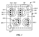
図1は、本明細書の以下に開示され、および、記載される一実施形態の1つ以上の特徴を有する電磁(EM)装置100の透過平面図を示す。一般に、EM装置100は、(以下に詳細が記載される)1つ以上の異なる方法で基板300に対して接着された少なくとも1つの誘電構造体200(参照符号200.1、200.2、200.3、200.4によって個々に参照される)を有する。一実施形態において、基板300は、基板300の第1の面304(図1の上面に示される)から反対の第2の面306(図1において示されていない下面、少なくとも図2Bを参照して最もよく理解される)に対して少なくとも部分的に延在する少なくとも1つのビア302を有する。一実施形態において、ビア302は、例えば図2A〜図2Cにおいて示されるz軸に沿って垂直であってよく、または、製造の変動によりわずかに垂直でなくてもよい。一実施形態において、誘電構造体200は、基板300の第1の面304から外側に延在する第1誘電部分204を形成する少なくとも1つの非気体誘電材料202を有し、第1誘電部分204は、平均誘電率を有する。基板300は、本明細書で誘電材料および導電性材料の積層物として示されている(本明細書の以下でさらに説明される)が、これは例示目的のためのみであること、また、他の形態の基板300では、限定されないが例えば、プリント基板(PCB)積層物、フレックスPCB、フレキシブルシート材料、ポリマー系シート材料、エレクトロニクスウェーハ材料、半導体ウェーハ、絶縁ウェーハ、または、金属シートが企図されることが理解されるであろう。一実施形態において、および、さらに詳細に以下の明細書で開示されるように、誘電構造体200は、誘電構造体200と少なくとも1つのビア302との間の界面において接着によって少なくとも部分的に基板300に対して接着され、少なくとも図1〜図9Bを参照して説明される。
FIG. 1 shows a transmission plan of an electromagnetic (EM)
一実施形態において、EM装置100は、誘電共振器アンテナ(DRA)であってもよく、誘電構造体200は、少なくともDRAの一部である。
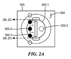
ここで図2A、2B、および2Cを参照すると、図2Aは、基板300上の誘電構造体200.1を示し、図2Bは、断面指示線2B−2Bを通る誘電構造体200.1の第1実施形態の側断面図を示し、および図2Cは、断面指示線2C−2Cを通る誘電構造体200.1の第2実施形態の側断面図を示す。少なくとも図1および図2Aに示されるように、誘電構造体200,200.1は、ビア302.1のうちの1つを部分的にのみ覆うように基板300の第1の面304に配置されるか、または、ビア302.2のうちの1つを完全に覆うように配置される。また、1つ以上の任意選択の二次ビア302.3(図1には、2つの二次ビア302.3のみが示され1つのみが挙げられているが、一実施形態は他の誘電構造体200と結合する他の二次ビア302.3を含んでもよい)は、例えば信号供給スロット324をはさんで誘電構造体200,200.1の反対側に配置されてもよい。二次ビア302.3は、ビア302.1,302.2と同じサイズまたは異なるサイズであってもよい。図2Bおよび図2Cの両方に示されるように、例示的なビア302は、基板300を完全に貫通して延在する。
In one embodiment, the
Here, referring to FIGS. 2A, 2B, and 2C, FIG. 2A shows the dielectric structure 200.1 on the
図2Bを参照して、非気体誘電材料202は、ビア302に部分的にのみ延在して欠肉したビアを形成する第2誘電部分206を形成するか、または、ビア302内に完全に延在して完全に充填されたビアを形成する第2誘電部分206,208を形成するか、または、ビア302内およびビア302を超えて完全に延在して過充填されたビアを形成する第2誘電部分206,208,210を形成し、第2誘電部分206,208,210は、第1誘電部分204と連続的であり、継ぎ目がない。一実施形態において、誘電構造体200は、誘電構造体200とビア302との間の界面102において接着によって基板300に対して部分的に接着されるだけでなく、第1誘電部分204と基板300の第1の面304との間の界面104において接着によって基板300に対してさらに接着される。過充填されたビア302の一実施形態において、基板300の第2の面306上のビア302の内径開口部308を超えて外側に延在する非気体誘電材料202の第3誘電部分212は、第3誘電部分212と基板300の第2の面306との間に肩つき連結部214を形成し、第3誘電部分212は第2誘電部分206,208,210と連続的であって継ぎ目がなく、誘電構造体200は、第3誘電部分212と基板300の第2の面306との間の界面214において接着によって基板300に対してさらに接着される。一実施形態において、基板300は、第1の面304上の第1導電層310、第2の面306上の第2導電層312、および第1導電層310と第2導電層312との間の誘電体層314を含み、ビア302は、第1導電層310と第2導電層312との間で電気的に接続された内壁316を有する。一実施形態において、図2Bに示されるように、誘電構造体200は、例えば、射出成形、圧縮成形、またはトランスファー成形などの成形プロセスによって加工されてもよい。代わりに、例えば、図2Bに示されるような誘電構造体200の一実施形態は熱積層プロセスによって加工されてもよい。
With reference to FIG. 2B, the non-gas
図2Cを参照すると、誘電構造体200は第1誘電部分204と基板300との間に配置された接着材料106を有し、ビア302は基板300を通って完全に延在し、接着材料は、(i)ビアの内部に部分的にのみ延在して、欠肉されたビアを形成して、破線108で表されるか、または(ii)ビア内に完全に延在して、完全に充填されたビアを形成して、破線110で表されるか、または(iii)ビア内に完全に延在し、かつ、超えて延在して過充填されたビアを形成して、破線112で表される。一実施形態において、接着材料106は平均誘電率を有し、接着材料106の誘電率と第1誘電部分204の誘電率とは、実質的に一致している。一実施形態において、誘電構造体200は、誘電構造体200とビア302との間の界面102において接着されることにより、基板300に対して部分的に接着されるだけでなく、第1誘電部分204と接着剤106との間の界面114および接着剤106と基板300の第1の面304との間の界面116において接着されることにより、基板300に対してさらに接着される。過充填されたビア302の一実施形態において、接着剤106の部分118は、接着剤106の部分118と基板300の第2の面306との間の肩つき連結部120を形成するように、基板300の第2の面306上のビア302の内径開口部308を超えて外側に延在する。図2Bに示される基板300と同様、図2Cに示される基板300は、また、第1の面304上の第1導電層310、第2の面306上の第2導電層312、および第1導電層310と第2導電層312との間の誘電体層314を含み、ビア302は、第1導電層310と第2導電層312との間で電気的に接続された内壁316を有する。一実施形態において、図2Cに示されるように、第1誘電部分204は、成形プロセスによって加工され、その後、接着剤106およびピックアンドプレースアセンブリプロセスによって基板300に接着されてもよい。
Referring to FIG. 2C, the
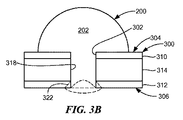
ここで、図3A、3B、および3Cを参照する。それぞれの図は以下の違いを除き、対応する図2A、2B、および2Cと同一である。一実施形態において、基板300は、第1の面304上の第1導電層310、第2の面306上の第2導電層312、および第1導電層310と第2導電層312との間の誘電体層314を有するが、ビア302は、第1導電層310と第2導電層312とを電気的に絶縁する非導電性内壁318を有する。図2A、図2B、および図2Cに示され、かつ、上に詳細に説明されたものと比較した図3A、図3B、および図3Cに示される構造の他の類似性を考慮して、当業者であれば、示された図を比較することによって同様の特徴を理解できるため、同様の特徴の繰り返しの説明は不要であると考えられる。
Here, reference is made to FIGS. 3A, 3B, and 3C. Each figure is identical to the corresponding figures 2A, 2B, and 2C, except for the following differences. In one embodiment, the
一実施形態において、および、図2B、2C、3B、および3Cに示されるように、ビア302の下部周囲の基板300の第2の面306は、面取り、端ぐり、または切り欠き322(図2B、2C、3B、および3Cに示されるが、明確にするために図3Bおよび3Cのみ列挙されている)を含んでもよく、それらは、非気体誘電材料202または接着材料106で充填されたとき、本明細書で上述した肩付き連結部214および120のものに加えて、別の形態の構造的取り付けを提供する。
In one embodiment, and as shown in FIGS. 2B, 2C, 3B, and 3C, the
ここで、図4Aおよび図4Bを参照すると、それぞれの図は以下の違いを除き、対応する図3Bおよび3Cと同一である。一実施形態において、ビア302は、第1導電層310および誘電体層314を完全に貫通して延在し、ビア302のブラインド端320を形成する第2導電層312で終結するブラインドビアである。ここで、図4Aに示される誘電構造体200を具体的に参照すると、非気体誘電材料202は、第1誘電部分204を形成するだけでなく、ブラインドビア302内に延在し、実質的に充填されたブラインドビア302を形成する第2誘電部分216もまた形成し、第2誘電部分216は、第1誘電部分204と連続的であって継ぎ目がない。ここで、図4Bに示される誘電構造体200を具体的に参照すると、接着材料106は、ブラインドビア302内に延在し、実質的に充填されたブラインドビア302を形成することが理解され得る。図3Bおよび図3Cに示され、かつ、上に詳細に説明されたものと比較した図4Aおよび図4Bに示される構造の他の類似性を考慮して、当業者であれば、示された図を比較することによって同様の特徴を理解できるため、同様の特徴の繰り返しの説明は不要であると考えられる。
Here, with reference to FIGS. 4A and 4B, the respective figures are identical to the corresponding FIGS. 3B and 3C, except for the following differences. In one embodiment, the via 302 is a blind via that extends completely through the first
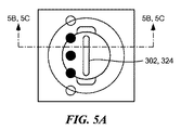
ここで、図5A、5B、および5Cを参照すると、それぞれの図は以下の違いを除き、対応する図3A、3B、および3Cと同様である。一実施形態において、および、図5Bを具体的に参照すると、基板300は、第1の面304上に導電層310、および、導電層310に隣接する誘電体層314を有する。図5A、5B,および5Cの実施形態において、例えば信号供給スロット324などの開いた領域は、導電層310を完全に貫通して延在し、ビア302のブラインド端320を形成する誘電体層314で終結するブラインドビアであるビア302のタイプを形成する。一実施形態において、この具体的なビア302,324は直線スロットまたは曲線スロットでもよく、代わりに例えば、正方形や円など両方の面内寸法(in−plane dimensions)が類似したものであってもよい。非気体誘電材料202は、第1誘電部分204を形成するだけでなく、ブラインドビア302に延在する第2誘電部分216をも形成して実質的に充填されたブラインドビア302を形成し、第2誘電部分216は、第1誘電部分204と連続的であり継ぎ目がない。別の実施形態において、および、図5Cを具体的に参照すると、誘電構造体200は、第1誘電部分204と基板300との間に配置された接着材料106を有する。基板300は、第1の面304上の導電層310、および、導電層310に隣接する誘電体層314を有する。ビア302は、導電層310を完全に貫通して延在するとともに、ビア302のブラインド端320を形成する誘電体層314で終結するブラインドビアである。接着材料106は、ブラインドビア302内に延在し、実質的に充填されたブラインドビア302を形成し、接着材料106の誘電率と第1誘電部分204の誘電率とは実質的に一致している。図3Bおよび3Cに示され、かつ、上に詳細に説明されたものと比較した図5Bおよび5Cに示される構造の他の類似性を考慮して、当業者であれば、示された図を比較することによって同様の特徴を理解できるため、同様の特徴の繰り返しの説明は不要であると考えられる。
Here, referring to FIGS. 5A, 5B, and 5C, each figure is similar to the corresponding figures 3A, 3B, and 3C, except for the following differences. In one embodiment and specifically with reference to FIG. 5B, the
ここで、図6A、6B、7A、および7Bを参照すると、これらの図および他の図に描かれている同様の要素には同じ番号が付されている。一実施形態において、および、図6Aを具体的に参照すると、EM装置100(例えば図1参照)は、第1の面304および反対の第2の面306を有する基板300と、基板300の第1の面304から外側に延在する誘電部分204を形成する少なくとも1つの非気体誘電材料202を有する誘電構造体200であって、誘電部分204が平均誘電率を有する誘電構造体200と、誘電部分204と基板300の第1の面304との間に配置された中間層122とを含み、誘電構造体200は、中間層122と基板300との間の界面124において接着されることによって、基板300に対して少なくとも部分的に接着される。さらにまた、誘電構造体200は、誘電部分204と中間層122との間の界面126において接着されることによって、基板300に対してさらに接着される。別の実施形態において、および図6Bを具体的に参照すると、誘電構造体200は、誘電部分204と中間層122との間に配置された接着材料106を有し、接着材料106の誘電率と誘電部分204の誘電率とは実質的に一致している。図6Aおよび6Bの両方に示されるように、中間層122は、誘電部分204と基板300の第1の面304との間の領域全体を覆い、それぞれ寸法128および寸法130で示されるように、誘電部分204の外縁を超えて延在しない場合もあれば、延在する場合もある。ここで具体的に図7Aおよび図7Bを参照する。中間層122は、誘電部分204と基板300の第1の面304との間の領域全体を覆い、寸法128で示されるように、誘電部分204の外縁を超えて延在しない。図6A、6B、7A、および7Bで示されるように、基板300は、第1の面304上に配置された導電層310、および、導電層310に隣接する誘電体層314を有し、導電層310は、中間層122と誘電体層314との間に配置される。一実施形態において、中間層122は、導電層310の平均表面粗さよりも大きい平均表面粗さを有する。一実施形態において、中間層122は、酸化物材料、酸化銅、黒色酸化物、窒化物材料、原子堆積材料の層、蒸着材料の層、または、前述の材料の任意の組み合わせで構成される。一実施形態において、最終中間層122は、中間層の形成中にマスキングされた堆積プロセスによって形成されてもよく、または、マスキングされた除去プロセスによる中間層材料の除去によって形成されてもよい。図7Aおよび7Bに示される実施形態に関して、エッチングプロセスは、寸法128によって示されるように、中間層122の終結を実質的に誘電構造体200の外縁において果たすために用いられてもよい。一実施形態において、エッチングプロセスは、酢酸エッチングプロセスでありうる。
Here, with reference to FIGS. 6A, 6B, 7A, and 7B, similar elements depicted in these and other figures are numbered the same. In one embodiment, and with reference to FIG. 6A specifically, the EM apparatus 100 (see, eg, FIG. 1) has a
ここで、以下の違いを除き、同様の要素には同じ番号が付され、図6A、6B、7A、および7Bの実施形態と同様の実施形態が示される図8Aおよび図8Bを参照する。一実施形態において、EM装置100(例えば図1を参照)は、導電層上または第1導電層310上に配置され、電気的に接続された金属化構造体400を含み、金属化構造体400は、複数の金属フェンスを形成し、複数の金属フェンスの各金属フェンス402は、誘電構造体200のうちの1つを取り囲むか、または実質的に取り囲む。一実施形態において、金属化構造体400は、誘電性の内側部分404および導電性の外側部分406を有する。図8Aおよび8Bにおいて破線132で示されるように、誘電構造体200と基板300との間の中間層122は、任意選択により、誘電構造体200から金属化構造体400に外側に延在してもよい。
Here, with reference to FIGS. 8A and 8B, similar elements are numbered the same except for the following differences and show similar embodiments to the embodiments of FIGS. 6A, 6B, 7A, and 7B. In one embodiment, the EM apparatus 100 (see, eg, FIG. 1) comprises a metallized
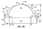
ここで、図9Aおよび9Bを参照する。図9AはEM装置100の透過平面図(例えば図1のEM装置100の誘電構造体200.3を参照)、図9Bは、図9Aの切断線9B−9Bを通る立面断面図である。一実施形態において、EM装置100は、第1の面304および反対の第2の面306を有する基板300と、基板300の第1の面304から外に延在する第1誘電部分204を形成する少なくとも1つの非気体誘電材料202を有する少なくとも1つの誘電構造体200とを含み、その誘電構造体200は、第1誘電部分204から横に延在する第2誘電部分(サイドウィング部分)218を形成する非気体誘電材料202をさらに含み、誘電構造体200は、第1誘電部分204と基板300との間の界面134において接着によって少なくとも部分的に基板300に接着され、前記EM装置100は、さらに第2誘電部分218と基板300との間の界面136を含む。一実施形態において、非気体誘電材料202は、第2誘電部分218と反対に第1誘電部分204から横に延在する第2誘電部分218と同様の第3誘電部分(サイドウイング部分)220をさらに形成し、誘電構造体200は、第3誘電部分220と基板300との間の界面138において基板300に対してさらに接着される。図9Aおよび9Bに示されるように、第2誘電部分218および第3誘電部分220は、第1誘電部分204から信号供給スロット324に沿って外側に横に延在し、誘電構造体200と基板300との間の追加の取り付け表面領域になるだけではなく、製造のばらつきにより、EM装置100の様々な部品または特徴に若干の不整合が生じる可能性がある非気体誘電材料202とともに,信号供給スロット324の適切なカバレッジを担保するためにも役立つ。一実施形態において、図9Bの平面図に認められるように、第1誘電部分204は、全体的な外形寸法Dを有し、第2誘電部分218および第3誘電部分220は、第1誘電部分204から距離dだけ横に延在し、dはDより小さい。一実施形態において、dはDの30%以下であるか、または、dはDの15%以下である。第2誘電部分218および第3誘電部分220は、図9Bにおいて、特定の平坦な頂部形状を有するように示されるが、これは例示目的のためだけであること、および、前記第2誘電部分218および前記第3誘電部分220は、本明細書に開示する目的のために、例えば破線222で表されるように基板300の第1の面304から誘電構造体200の頂点224への漸進的な遷移形状などの好適な任意の形状を有してもよいことが理解されるであろう。一実施形態において、第2誘電部分218および第3誘電部分220の高さhは、誘電構造体200の全体の高さHよりも低い。一実施形態において、hはHの30%以下であるか、またはhはHの15%以下である。
Here, reference is made to FIGS. 9A and 9B. 9A is a transmission plan view of the EM device 100 (see, for example, the dielectric structure 200.3 of the
図8Aおよび8Bに示される金属化構造体400は、例えば図6A、6B、7Aおよび7Bに示される誘電構造体200と同様のものなどの特定の誘電構造体200に関連して示されるが、同じ金属化構造体400が本明細書に開示される例えば図2B、2C、3B、3C、4A、4B、5B、5C、9Aおよび9Bに示されるものなどの任意の他の誘電構造体200に適用可能であると出願人は考えているので、そのような描写は例示目的のみであり、本開示の範囲を限定することを意図していないことが理解されるであろう。
The metallized
前述の実施形態のうちのいずれにおいても、本明細書に開示される目的に好適な当該技術分野で既知の任意の信号供給構造体が本明細書に開示される誘電構造体200を電磁的に励起するために実装されうることが理解されるであろう。そうとは言え、本明細書に開示される一実施形態は、図1に示されるように、第1導電層310と第2導電層312との間で電気的に接続された内壁316を有するビア302が基板統合導波路(SIW)140を形成する配置を含む。一実施形態において、二次ビア302.3は、SIW140の動作を妨害しないように非金属メッキでありうる。
In any of the aforementioned embodiments, any signal supply structure known in the art suitable for the purposes disclosed herein electromagnetically displaces the
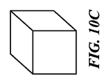
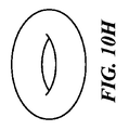
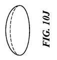
本明細書に開示される様々な誘電構造体200は、代表的なドーム形状または半球形状を有し、したがってz軸に対して円形の断面を有するが、これは例示目的のためのみであること、および本開示の範囲を損なうことなく、誘電構造体200の他の形状が使用されてもよいことが理解されるであろう。図10A〜図11Dを例えば参照して、開示された任意の誘電構造体200は、円筒形の三次元形状の図10A、多角形ボックスの図10B、10C、先細の多角形ボックスの図10D、10E、円錐の図10F、円錐台の図10G、トロイドの図10H、ドームの図10I(例えば半球)、細長のドームの図10J、または、本明細書に開示される目的のために好適な任意の他の三次元形状を有してもよく、したがって、円形状の図11A、長方形状の図11B、多角形状の図11C、リング状の図11D、楕円状の図11E、または本明細書に開示される目的にために好適な他の形状のz軸断面を有してもよい。
The various
加えて、図1は、特定の方法で配置された誘電構造体200.1,200.1,200.3,200.4のアレイとしてのEM装置100を示すが、これは例示のみの目的であること、および本開示の範囲を損なうことなく誘電構造体200の他の配置が使用されてもよいことが理解されるであろう。図12A〜図12Gを例えば参照して複数の誘電構造体200は、以下の配置のいずれかにしたがって隣接する誘電構造体200の間に中心―中心間距離でアレイに配置されてもよい。x−yグリッド構造において互いに等間隔に配置され、A=B(例えば図12Aを参照)。ダイアモンド形態において間隔をおいて配置され、ダイアモンド形態のダイアモンド形状は向かい合う内角α<90度および向かい合う内角β>90度を有する(例えば図12B参照)。均一な周期的パターンで互いに対して間隔をおいて配置される(例えば図12A、12B、12C、12D参照)。増加または減少する非周期的パターンで互いに対して間隔をおいて配置される(例えば図12E、12F、12Gを参照)。均一な周期的パターンで斜めのグリッド上に互いに対して間隔をおいて配置される(例えば図12Cを参照)。均一な周期的パターンで放射状グリッド上で互いに対して間隔をおいて配置される(例えば図12Dを参照)。増加または減少する非周期的パターンでx−yグリッド上で互いに対して間隔をおいて配置される(例えば図12Eを参照)。増加または減少する非周期的パターンで斜めのグリッド上に互いに対して間隔をおいて配置される(例えば、図12Fを参照)。増加または減少する非周期的パターンで放射状グリッド上で互いに対して間隔をおいて配置される(例えば、図12Gを参照)。均一な周期的パターンで非x−yグリッド上で互いに対して間隔をおいて配置される(例えば、図12B、12C、12Dを参照)。増加または減少する非周期的パターンで非x−yグリッド上で互いに対して間隔をおいて配置される(例えば、図12F、12Gを参照)。複数の誘電構造体200の様々な配置は、例えば図12A〜図12Gを介して示されるが、そのような示された配置は本明細書に開示される目的と一致して構成されうる多くの配置を論じ尽くしてはいないことが理解されるであろう。つまり、本明細書に開示される目的のために本明細書に開示される複数の誘電構造体200の任意の配置およびすべての配置は、本明細書に開示される開示の範囲内であると企図され、考えられる。
In addition, FIG. 1 shows the
プリント基板またはシリコンウェーハなどの回路基板上に構造を形成するためのインサート成形などの成形プロセスでは、成形材料と基板との間の接着が弱くなることが多い。しかしながら、そのような適用では、良好な電気的応答を得るためには、成形材料と下にある基板との間の強力な接着が重要である。例えば、基板300上に誘電構造体200を射出成形することは、数マイクロメートルの長さスケールに沿って層間剥離領域を生じることが多い。誘電構造体の誘電材料と導電層との間の接着、または誘電構造体の誘電材料と誘電体層の誘電材料との間の接着は、機械的手法または化学的手法のうちの一方または両方によって向上させられることが見出された。機械的手法は、ビアの逆行性表面を利用して誘電構造体と導電層および誘電体層のうちの少なくとも1つとを機械的に連結することを含む。化学的手法には、導電層の表面の酸化または接着剤層の追加が含まれる。接着性を高めるための別の手法は、誘電構造体と導電層との間の界面領域を増やすために導電層の表面を粗くすることを含む。
In a molding process such as insert molding for forming a structure on a circuit board such as a printed circuit board or a silicon wafer, the adhesion between the molding material and the substrate is often weakened. However, in such applications, strong adhesion between the molding material and the underlying substrate is important in order to obtain a good electrical response. For example, injection molding a
誘電構造体200は、誘電組成物を基板300上に例えばインサート成形などの射出成形によって、形成され得る。いくつかの実施形態においては、複数の誘電構造体は、例えば導電層310および誘電体層314を含む、基板300上に射出成形される。成形と、例えば3D印刷またはインクジェット印刷のうちの少なくとも1つなどの他の製造方法とを組み合わせて使用することもできる。
The
射出成形は、誘電構造体の基板への迅速かつ効率的な製造を可能にする。射出成形は、基板の表面に配置された金型に基板を配置すること、および誘電組成物を金型に射出成形することを含み得る。 Injection molding allows for the rapid and efficient production of dielectric structures on substrates. Injection molding can include placing the substrate in a mold located on the surface of the substrate and injection molding the dielectric composition into the mold.
成形は、熱可塑性ポリマーを含む誘電組成物を射出成形することを含み得る。誘電組成物は、初めに誘電性充填剤と任意選択のシランとを組み合わせて充填剤組成物を形成し、その後、充填剤組成物を熱可塑性ポリマーと混合することによって調製され得る。熱可塑性ポリマーの場合、ポリマーは、誘電性充填剤のうちの一方または両方との混合前、混合後、または混合中に溶融することができる。次に、誘電組成物を金型内で射出成形することができる。誘電組成物は、その後、金型内に射出成形され得る。 Molding may include injection molding a dielectric composition containing a thermoplastic polymer. The dielectric composition can be prepared by first combining a dielectric filler with an optional silane to form a filler composition and then mixing the filler composition with a thermoplastic polymer. In the case of thermoplastic polymers, the polymer can be melted before, after, or during mixing with one or both of the dielectric fillers. Next, the dielectric composition can be injection molded in the mold. The dielectric composition can then be injection molded into the mold.
溶融温度、射出温度、および金型温度は、ポリマーの溶融温度およびガラス転移温度に依存し得る。溶融温度、射出温度、および金型温度は、ポリマーの溶融温度およびガラス転移温度のうちの少なくとも1つより高いか、または等しい。溶融温度、射出温度、および金型温度のうちの少なくとも1つは、40℃〜220℃、または40℃〜160℃、または100℃〜220℃であり得る。射出圧力および保持圧力の一方または両方は65〜350キロパスカル(kPa)であり得る。 The melting temperature, injection temperature, and mold temperature can depend on the melting temperature of the polymer and the glass transition temperature. The melting temperature, injection temperature, and mold temperature are greater than or equal to at least one of the polymer melting temperature and glass transition temperature. At least one of the melting temperature, injection temperature, and mold temperature can be 40 ° C to 220 ° C, or 40 ° C to 160 ° C, or 100 ° C to 220 ° C. One or both of the injection pressure and the holding pressure can be 65-350 kilopascals (kPa).
超音波は、射出成形を促進するために使用され得る。例えば、超音波は、誘電組成物または基板に集中させることができる。生じた力は、充填剤の濡れ性の改善、誘電組成物の粘度の低減、圧縮密度の改善、または誘電組成物と基板との間の界面接着の改善または増加のうちの少なくとも1つをもたらし得る。 Ultrasound can be used to facilitate injection molding. For example, ultrasonic waves can be concentrated on a dielectric composition or substrate. The force generated results in at least one of improved wettability of the filler, reduced viscosity of the dielectric composition, improved compression density, or improved or increased interfacial adhesion between the dielectric composition and the substrate. obtain.
超音波の使用に代えて、射出成形を促進するために超音波の代わりに熱エネルギーが使用されてもよい。例えば、結合された基板は、誘電組成物をオーバーモールドし、または加熱する前に、および基板上に誘電構造体を接着する前に予熱されてもよい。 Instead of using ultrasonic waves, thermal energy may be used instead of ultrasonic waves to facilitate injection molding. For example, the bonded substrate may be preheated before overmolding or heating the dielectric composition and before adhering the dielectric structure onto the substrate.
金型を充填するために0.1〜10秒、または0.5〜5秒、または0.2〜1秒かかり得、その間、金型温度は下がり得る。金型は、1秒あたり0.25〜3立方インチ(in3/sec)の速度で充填され得る。射出後、誘電組成物は、10分以下または2分以下、または2〜30秒、または0.5〜10分、または0.5〜5分金型内にあり得る。成形後、低下した金型温度において装置を取り外すことができる。 It can take 0.1-10 seconds, or 0.5-5 seconds, or 0.2-1 seconds to fill the mold, during which the mold temperature can drop. The mold can be filled at a rate of 0.25 to 3 cubic inches (in 3 / sec) per second. After injection, the dielectric composition can be in the mold for 10 minutes or less, 2 minutes or less, or 2 to 30 seconds, or 0.5 to 10 minutes, or 0.5 to 5 minutes. After molding, the device can be removed at a reduced mold temperature.
様々な変数は、誘電組成物の良好な成形を確実にするために変更され得る。例えば、以下の変数のうちの少なくとも1つが変更され得る。射出速度、射出中のノズルの位置、ノズルのサイズ、誘電組成物の粘度、射出成形材料の(例えば、熱可塑性ポリマーまたは硬化性組成物中のオリゴマーの)分子量、充填剤組成物(例えば、マルチモーダル粒子サイズを使用する)、温度(例えば、成形前の誘電組成物の温度、成形中の射出温度、または金型の金型温度)、または圧力。 Various variables can be modified to ensure good molding of the dielectric composition. For example, at least one of the following variables can be modified. Injection rate, nozzle position during injection, nozzle size, dielectric composition viscosity, molecular weight of injection molding material (eg, oligomers in thermoplastic polymers or curable compositions), filler composition (eg mulch). Modal particle size (using modal particle size), temperature (eg, temperature of the dielectric composition before molding, injection temperature during molding, or mold temperature of the mold), or pressure.
導電層310は、逆行性表面を有する連結スロット510を含み得る。連結スロットの逆行性表面は、誘電構造体200と導電層310との間の機械的連結を生じ得る。逆行性表面のある連結スロット510の一例は、図13に示される。図13に示されるように、上部開口部502の断面領域は、連結スロット510の深さに沿った位置における断面領域よりも小さい断面領域を有し得る。上部開口部は、射出成形中にそれを通って誘電組成物が入る開口部として定義される。
The
連結スロット510の逆行性表面は、基板300の成形面504に対して90°未満、または10〜85°、または45〜80°の角度θに沿って線形であり得る。基板の成形面は、誘電組成物が射出成形される面を表す。図13は、線形逆行性表面の一実施形態を示す。逆行性表面は、例えば凸面または凹面のうちの少なくとも1つを有し、非線形であり得る。逆行性表面は、例えば粗面または逆行性表面の内外に延在する複数の突出部を含むように、ぎざぎざにされ得る。
The retrograde surface of the
逆行性表面は、様々な方法で形成され得る。例えば、逆行性表面は、例えば、マスキングにより、エッチャントに対して第1導電層310の領域をさらすことによって形成され得る。エッチングは、液体エッチャントを使用して行うことができる。エッチングは、気相のエッチャントを使用して、例えばプラズマエッチング、イオンビームエッチング、または反応性イオンエッチングのうちの少なくとも1つによって行うことができる。エッチャントは等方的に、すなわち横方向と縦方向の両方でエッチングすることができる。等方性エッチャント(例えば、塩素ガスまたは塩化水素)は、線形の逆行性表面または凹状の逆行性表面の形成をもたらし得る。
Retrograde surfaces can be formed in a variety of ways. For example, the retrograde surface can be formed by exposing the region of the first
前述の導電層のうちのいずれかは、例えば導電層310および導電層312は独立して、導電性金属を含み得る。導電性金属は、銅、アルミニウム、銀、または金のうちの少なくとも1つを含み得る。例えば、導電性金属は銅または銅合金を含み得る。
In any of the above-mentioned conductive layers, for example, the
インサート成形の前に、中間層122は、導電層310上に形成され得る。同様に、中間層は、ビア302の任意の露出したブラインド端320上に形成され得る。中間層122は、酸化物材料(例えば酸化銅または黒色酸化物のうちの少なくとも1つ)、窒化物材料、原子堆積材料の層、または蒸着材料の層のうちの少なくとも1つを含み得る。中間層122は原子堆積または蒸着のうちの少なくとも1つによって形成され得る。中間層122は、導電層をHNO3、H2SO4、AgNO3、H2O2、HOCl、KOCl、KMnO4、またはCH3COOHのうちの少なくとも1つを含む水溶性の酸化性溶液にさらすことによって形成され得る。酸化性溶液は、酸化性溶液の総体積を基準として、2〜95vol%、または5〜80vol%の酸化剤を含み得る。中間層は、導電層と比較して増加した粗さを有し得る。中間層は、0.5〜5マイクロメートル、または1〜5マイクロメートル、または1〜3マイクロメートルのピーク部から谷底部までの平均距離を有する粗さを含み得る。ピーク部から谷底部までの平均距離は、例えば、走査型電子顕微鏡法を使用して得られた少なくとも20マイクロメートル四方の領域を有する表面の部分の画像の画像分析を使用して決定され得る。ピーク部から谷底部までの平均距離を決定する他の方法には、光学式粗さ計および原子間力顕微鏡法が含まれる。
Prior to insert molding, the
インサート成形の前に、導電層の表面、例えば、成形面504は、初めの表面と比較して増加したピーク部から谷底部までの平均距離を有する粗面化表面を形成するように機械的または化学的プロセスによって粗くされ得る。ピーク部から谷底部までの平均距離は、導電層の厚さの5%以上、または10%以上、または20〜50%であり得る。この粗さの増加により、誘電構造体の接着性を向上させることが可能であり得る。
Prior to insert molding, the surface of the conductive layer, eg, the
インサート成形の前に、接着材料106は、基板の成形面上に、例えば、導電層310、中間層122、任意の露出した誘電体層314、またはビア302の任意の露出したブラインド端のうちの少なくとも1つの上に、堆積され得る。接着剤層は、所望の特性に基づいて選択することができ、例えば、2つの誘電体層または導電層を誘電体層に接着するための低融点または他の組成物を有する熱硬化性ポリマーであり得る。接着層は、ポリ(アリーレンエーテル)、ブタジエン、イソプレン、またはブタジエンおよびイソプレン単位を含むカルボキシ官能化ポリブタジエンポリマーまたはカルボキシ官能化ポリイソプレンポリマーおよび0〜50wt%以下の共硬化性モノマー単位を含むことができる。接着剤層の接着剤組成は、誘電組成物とは異なり得る。接着剤層は、1平方メートルあたり2〜15グラムの量で存在し得る。ポリ(アリーレンエーテル)は、カルボキシ官能化ポリ(アリーレンエーテル)を含み得る。ポリ(アリーレンエーテル)は、ポリ(アリーレンエーテル)と環状無水物との反応生成物、またはポリ(アリーレンエーテル)と無水マレイン酸との反応生成物であり得る。カルボキシ官能化ポリブタジエンポリマーまたはカルボキシ官能化ポリイソプレンポリマーは、カルボキシ官能化ブタジエン−スチレンコポリマーであり得る。カルボキシ官能化ポリブタジエンポリマーまたはカルボキシ官能化ポリイソプレンポリマーは、ポリブタジエンポリマーまたはポリイソプレンポリマーと環状無水物との反応生成物であり得る。カルボキシ官能化ポリブタジエンポリマーまたはカルボキシ官能化ポリイソプレンポリマーは、マレイン化ポリブタジエン−スチレンコポリマーまたはマレイン化ポリイソプレン−スチレンコポリマーであり得る。
Prior to insert molding, the
接着剤層は、その誘電率を調整するための誘電性充填剤(例えばセラミック粒子)を含むことができる。例えば、接着剤層の誘電率は、電磁装置(例えばDRA装置)の性能を改善またはさもなければ変更するように調整され得る。 The adhesive layer can contain a dielectric filler (eg, ceramic particles) for adjusting its dielectric constant. For example, the dielectric constant of the adhesive layer can be adjusted to improve or otherwise change the performance of the electromagnetic device (eg, DRA device).
それぞれの誘電体部分、例えば、誘電構造体200および誘電体層314は、各々独立して誘電材料を含み得る。前述の実施形態のうちのいずれかにおいて、多種多様な誘電材料が使用され得る。誘電構造体は、熱可塑性ポリマーを含み得る。誘電体層314は、熱可塑性ポリマーまたは熱硬化性ポリマーのうちの少なくとも1つを含み得る。誘電材料は、誘電性充填剤(本明細書で充填剤とも言及される)を含有する充填剤組成物を含み得る。各誘電材料は、独立して、誘電材料の総体積を基準として、30〜100体積パーセント(vol%)のポリマー、および0〜70vol%の充填剤組成物、または30〜99vol%のポリマーおよび1〜70vol%の充填剤組成物、または50〜95vol%のポリマーおよび5〜50vol%の充填剤組成物を含み得る。ポリマーおよび充填剤は、本明細書に開示される目的のために矛盾していない誘電率と、10ギガヘルツ(GHz)において0.01未満、または0.008以下である誘電正接とを有する誘電材料を提供するように選択され得る。誘電正接は、IPC−TM−650 X−バンドストリップライン法によって、またはスプリット共振器法によって測定され得る。
Each dielectric moiety, for example the
熱可塑性ポリマーは、オリゴマー、ポリマー、イオノマー、デンドリマー、コポリマー(例えば、グラフトコポリマー、ランダムコポリマー、ブロックコポリマー(例えば、スターブロックコポリマーおよびランダムコポリマー))、および前述のうちの少なくとも1つを含む組み合わせを含み得る。熱可塑性ポリマーは、半結晶性または非晶性であり得る。熱可塑性ポリマーは、23℃で500MHz〜100GHz、または500MHz〜10GHzの周波数で0.007以下、または0.006以下、または0.0001〜0.007の誘電損失(誘電正接とも言及される)を有し得る。 Thermoplastic polymers include oligomers, polymers, ionomers, dendrimers, copolymers (eg, graft copolymers, random copolymers, block copolymers (eg, starblock copolymers and random copolymers)), and combinations comprising at least one of the aforementioned. obtain. The thermoplastic polymer can be semi-crystalline or amorphous. Thermoplastic polymers have a dielectric loss of 0.007 or less, or 0.006 or less, or 0.0001 to 0.007 (also referred to as dielectric loss tangent) at frequencies of 500 MHz to 100 GHz at 23 ° C. or 500 MHz to 10 GHz. Can have.
熱可塑性ポリマーは、ポリカーボネート、ポリスチレン、ポリ(フェニレンエーテル)、ポリイミド(例えば、ポリエーテルイミド)、ポリブタジエン、ポリアクリロニトリル、ポリ(C1−12アルキル)メタクリレート(例えば、ポリメチルメタクリレート(PMMA))、ポリエステル(例えば、ポリ(エチレンテレフタレート)、ポリ(ブチレンテレフタレート)、ポリチオエステル)、ポリオレフィン(例えば、ポリプロピレン(PP)、高密度ポリエチレン(HDPE)、低密度ポリエチレン(LDPE)、直鎖状低密度ポリエチレン(LLDPE))、ポリアミド(例えば、ポリアミドイミド)、ポリアリレート、ポリスルホン(例えば、ポリアリールスルホン、ポリスルホンアミド)、ポリ(フェニレンサルファイド)、ポリ(フェニレンオキシド)、ポリエーテル(例えば、ポリ(エーテルケトン)(PEK)、ポリ(エーテルエーテルケトン)(PEEK)、ポリエーテルスルホン(PES))、ポリ(アクリル酸)、ポリアセタール、ポリベンゾオキサゾール(例えば、ポリベンゾチアゾール、ポリベンゾチアジノフェノチアジン(polybenzothiazinophenothiazine))、ポリオキサジアゾール、ポリピラジノキノキサリン(polypyrazinoquinoxaline)、ポリピロメリットイミド、ポリキノキサリン、ポリベンズイミダゾール、ポリオキシンドール、ポリオキソイソインドリン(例えば、ポリジオキソイソインドリン)、ポリトリアジン、ポリピリダジン、ポリピペラジン、ポリピリジン、ポリピペリジン、ポリトリアゾール、ポリピラゾール、ポリピロリジン、ポリカーボレーン(polycarborane)、ポリオキサビシクロノナン(polyoxabicyclononane)、ポリジベンゾフラン、ポリフタリド(polyphthalide)、ポリアセタール、ポリ無水物、ビニルポリマー(例えば、ポリ(ビニルエーテル)、ポリ(ビニルチオエーテル)、ポリ(ビニルアルコール)、ポリ(ビニルケトン)、ポリ(ハロゲン化ビニル)(例えば、ポリ(塩化ビニル))、ポリ(ビニルニトリル)、ポリ(ビニルエステル))、ポリスルホン酸塩、ポリスルフィド、ポリ尿素、ポリホスファゼン、ポリシラザン、ポリシロキサン、または前述のうちの少なくとも1つを含む組み合わせを含み得る。熱可塑性ポリマーは、ポリ(アリール)エーテルケトン(例えば、ポリ(エーテルケトン)、ポリ(エーテルエーテルケトン)、およびポリ(エーテルケトンケトン))、ポリスルホン(例えば、ポリ(エーテルスルホン))、ポリ(フェニレンサルファイド)、ポリ(エーテルイミド)、ポリ(アミドイミド)、または前述のうちの少なくとも1つを含む組み合わせを含み得る。熱可塑性ポリマーは、ポリオレフィンを含み得る。熱可塑性ポリマーは、前述のポリマーのうちの少なくとも1つを含む組み合わせを含み得る。 Thermoplastic polymers include polycarbonate, polystyrene, poly (phenylene ether), polyimide (eg, polyetherimide), polybutadiene, polyacrylonitrile, poly (C 1-12 alkyl) methacrylate (eg, polymethylmethacrylate (PMMA)), polyester. (For example, poly (ethylene terephthalate), poly (butylene terephthalate), polythioester), polyolefin (eg, polypropylene (PP), high density polyethylene (HDPE), low density polyethylene (LDPE), linear low density polyethylene (LLDPE). )), Polyamide (eg, polyamideimide), polyarylate, polysulfone (eg, polyarylsulfone, polysulfoneamide), poly (phenylene sulfide), poly (phenylene oxide), polyether (eg, poly (etherketone) (PEK). ), Poly (etheretherketone) (PEEK), polyethersulfone (PES)), poly (acrylic acid), polyacetal, polybenzoxazole (eg, polybenzothiazole, polybenzothiazinophenothiazine), polyoxa Diazole, polypyrazinoquinoxaline, polypyrromeridimide, polyquinoxaline, polybenzimidazole, polyoxindole, polyoxoisoindolin (eg, polydioxoisoindolin), polytriazine, polypyridazine, polypiperazin, polypyridine, Polypiperidin, polytriazole, polypyrazole, polypyrrolidin, polycarborane, polyoxavicyclonone, polydibenzofuran, polyphthalide, polyacetylide, polyacetal, polyanhydride, vinylpolymer (eg, polyvinyl ether). Poly (vinyl thioether), poly (vinyl alcohol), poly (vinyl ketone), poly (vinyl halide) (eg, poly (vinyl chloride)), poly (vinyl nitrile), poly (vinyl ester)), polysulfonate, It may include polysulfide, polyurea, polyphosphazene, polysilazane, polysiloxane, or a combination comprising at least one of the aforementioned. Thermoplastic polymers include poly (aryl) ether ketones (eg, poly (ether ketones), poly (ether ether ketones), and poly (ether ketone ketones)), polysulfones (eg, poly (ether sulfones)), poly (phenylenes). Sulfide), poly (etherimide), poly (amideimide), or combinations comprising at least one of the aforementioned may be included. The thermoplastic polymer may include polyolefins. The thermoplastic polymer may include a combination comprising at least one of the aforementioned polymers.
熱可塑性ポリマーは、ポリ(アリール)エーテルケトン、例えば、ポリ(エーテルケトン)、ポリ(エーテルエーテルケトン)、およびポリ(エーテルケトンケトン)を含み得る。例えば、熱可塑性ポリマーは、ポリ(エーテルエーテルケトン)を含み得る。ポリ(エーテルエーテルケトン)は、400℃において2.16キログラム(kg)の負荷で、ASTM D1238−13、手順Aに従って特定されたように、10分あたり40〜50グラム(g/10分)のメルトフローレート(MRF)を有し得る。 Thermoplastic polymers can include poly (aryl) etherketones, such as poly (etherketone), poly (etheretherketone), and poly (etherketoneketone). For example, the thermoplastic polymer may include poly (etheretherketone). Poly (etheretherketone) is 40-50 grams (g / 10 min) per 10 minutes, as identified according to ASTM D1238-13, Procedure A, at a load of 2.16 kg (kg) at 400 ° C. It may have a melt flow rate (MRF).
熱可塑性ポリマーは、ポリオレフィンを含み得る。ポリオレフィンは、低密度ポリエチレンを含み得る。ポリオレフィンは、環状オレフィンコポリマー(例えば、メタロセン触媒を使用したノルボルネンおよびエチレンの共重合生成物)、任意選択で直鎖状ポリオレフィンとの組み合わせを含み得る。環状オレフィンコポリマーは、ISO527−2/1A:2012に従って測定されたように、1分あたり5ミリメートル(mm/分)で40〜50メガパスカル(MPa)の降伏点引張強度、IEC 60250に従って特定されたように1〜10キロヘルツ(kHz)の周波数で2〜2.5の誘電率、およびISO75−1,−2:2004に従って特定されたように、0.46MPaにおいて125℃以上の例えば、135〜160℃の加熱撓み温度のうちの1つ以上を有し得る。 The thermoplastic polymer may include polyolefins. Polyolefins can include low density polyethylene. Polyolefins may include cyclic olefin copolymers (eg, metallocene-catalyzed copolymers of norbornene and ethylene), optionally in combination with linear polyolefins. Cyclic olefin copolymers were identified according to IEC 60250, a yield point tensile strength of 40-50 megapascals (MPa) at 5 millihertz (mm / min) per minute, as measured according to ISO 527-2 / 1A: 2012. Permittivity of 2 to 2.5 at frequencies of 1 to 10 kHz (kHz), and, for example, 135-160 above 125 ° C. at 0.46 MPa, as specified according to ISO75-1, -2: 2004. It can have one or more of the heating deflection temperatures of ° C.
誘電材料は、液晶ポリマーを含み得る。液晶ポリマー(「LCP」と略されることがある)は、様々な用途でよく知られているポリマー類である。液晶ポリマーは、熱可塑性樹脂を含むことが多いが、官能化によって、または熱硬化性樹脂、例えばエポキシと混合することによって、熱硬化性樹脂としても使用することもできる。液晶ポリマーは、高分子鎖の繰り返し単位の性質により、固定された分子形状(たとえば、直鎖状)を持っていると考えられている。繰り返し単位は、典型的には、堅い分子要素を含む。堅い分子要素(メソゲン)は、しばしば棒状または円盤状の形状であり、典型的には芳香族であり、しばしば複素環式である。堅い分子要素は、ポリマーの主鎖(骨格)および側鎖の一方または両方に存在し得る。堅い分子要素は、スペーサーと言及されることのある、より柔軟な分子要素によって隔てられ得る。 The dielectric material may include a liquid crystal polymer. Liquid crystal polymers (sometimes abbreviated as "LCP") are polymers that are well known for a variety of applications. The liquid crystal polymer often contains a thermoplastic resin, but can also be used as a thermosetting resin by functionalization or by mixing with a thermosetting resin such as an epoxy. Liquid polymer is considered to have a fixed molecular shape (eg, linear) due to the nature of the repeating unit of the polymer chain. Repeat units typically include rigid molecular elements. Rigid molecular elements (mesogens) are often rod-shaped or disc-shaped, typically aromatic, and often heterocyclic. Rigid molecular elements can be present in one or both of the main and side chains of the polymer. Rigid molecular elements can be separated by more flexible molecular elements, sometimes referred to as spacers.
市販の液晶ポリマーの例には、限定はされないが、VECTRA(商標)、Celaneseから市販、XYDAR(商標)、Solvayから市販、およびZENITE(商標)、Celaneseから市販、およびRTP Co.から入手可能なもの、例えば、RTP−3400シリーズ液晶ポリマーが含まれる。 Examples of commercially available liquid crystal polymers include, but are not limited to, VECTRA ™, Celanese to market, XYDAR ™, Solvay to market, and ZENITE ™, Celanese to market, and RTP Co., Ltd. Included are those available from, for example, RTP-3400 series liquid crystal polymers.
誘電材料は、1,2−ポリブタジエン(PBD)、ポリイソプレン、ポリブタジエン−ポリイソプレンコポリマー、ポリエーテルイミド(PEI)、ポリテトラフルオロエチレン(PTFE)などのフルオロポリマー、ポリイミド、ポリエーテルエーテルケトン(PEEK)、ポリアミドイミド、ポリエチレンテレフタレート(PET)、ポリエチレンナフタレート、ポリシクロヘキシレンテレフタレート、または、アリル化ポリフェニレンエーテルをベースとしたものなどのポリフェニレンエーテルのうちの少なくとも1つを含み得る。低極性ポリマーと高極性ポリマーの組み合わせもまた使用され得、非限定的な例として、エポキシおよびポリ(フェニレンエーテル)、エポキシおよびポリ(エーテルイミド)、シアン酸エステルおよびポリ(フェニレンエーテル)、または1,2−ポリブタジエンおよびポリエチレンが挙げられる。 The dielectric material is 1,2-polybutadiene (PBD), polyisoprene, polybutadiene-polyisoprene copolymer, polyetherimide (PEI), fluoropolymer such as polytetrafluoroethylene (PTFE), polyimide, polyetheretherketone (PEEK). , Polyimideimide, polyethylene terephthalate (PET), polyethylene naphthalate, polycyclohexylene terephthalate, or at least one of polyphenylene ethers such as those based on allylated polyphenylene ethers. Combinations of low polar and high polar polymers can also be used, with non-limiting examples being epoxy and poly (phenylene ether), epoxy and poly (etherimide), cyanate and poly (phenylene ether), or 1 , 2-Polybutadiene and polyethylene.
誘電体層314は、例えばポリフッ化ビニル(PVF)、ポリフッ化ビニリデン(PVDF)、フッ素化エチレン−プロピレン(FEP)、ポリテトラフルオロエチレン(PTFE)、またはポリエチレンテトラフルオロエチレン(PETFE)などのフルオロポリマーを含み得る。フルオロポリマーは、例えば、PTFEおよびポリクロロトリフルオロエチレン(PCTFE)などのフッ素化ホモポリマー、および、例えば、テトラフルオロエチレンまたはクロロトリフルオロエチレンと、ヘキサフルオロプロピレンまたはパーフルオロアルキルビニルエーテル、フッ化ビニリデン、フッ化ビニル、エチレン、または上記のうちの少なくとも1つを含む組み合わせなどのモノマーとのコポリマーなどのフッ素化コポリマーを含む。フルオロポリマーは、これらのフルオロポリマーのうちの少なくとも1つの異なる組み合わせを含むことができる。
The
誘電体層314は、熱硬化性ポリブタジエンおよび熱硬化性ポリイソプレンを含み得る。本明細書に使用されるとき、用語「熱硬化性ポリブタジエンまたは熱硬化性ポリイソプレン」は、ブタジエン、イソプレン、またはそれらの組み合わせから誘導される単位を含むホモポリマーおよびコポリマーを含む。他の共重合可能なモノマーから誘導される単位もまた、例えばグラフトの形態でポリマー中に存在し得る。例示的な共重合可能なモノマーには、限定はされないが、ビニル芳香族モノマー、例えば、スチレン、3−メチルスチレン、3,5−ジエチルスチレン、4−n−プロピルスチレン、アルファ−メチルスチレン、アルファ−メチルビニルトルエン、パラ−ヒドロキシスチレン、パラ−メトキシスチレン、アルファ−クロロスチレン、アルファ−ブロモスチレン、ジクロロスチレン、ジブロモスチレン、テトラ−クロロスチレンなどの置換および非置換モノビニル芳香族モノマーおよびジビニルベンゼン、ジビニルトルエンなどの置換および非置換ジビニル芳香族モノマーが含まれる。前述の共重合可能なモノマーのうちの少なくとも1つを含む組み合わせも、また使用され得る。例示的な熱硬化性ポリブタジエンまたは熱硬化性ポリイソプレンは、限定はされないが、ブタジエンホモポリマー、イソプレンホモポリマー、ブタジエン−スチレンなどのブタジエン−ビニル芳香族コポリマー、イソプレン−スチレンコポリマーなどのイソプレン−ビニル芳香族コポリマーなどを含む。
The
熱硬化性ポリブタジエンまたは熱硬化性ポリイソプレンはまた、変更され得る。例えば、ヒドロキシル末端、メタクリレート末端、カルボキシル末端などであり得る。ブタジエンポリマーまたはイソプレンポリマーのエポキシ修飾ポリマー、無水マレイン酸修飾ポリマー、またはウレタン修飾ポリマーなどの事後反応ポリマーが使用され得る。ポリマーはまた、例えば、ジビニルベンゼンなどのジビニル芳香族化合物(例えばジビニルベンゼンで架橋されたポリブタジエン−スチレンなど)によって架橋することができる。例示的な材料は、Nippon Soda Co.、東京、日本、およびCray Valley Hydrocarbon Specialty Chemicals、エクストン、PAなどの製造業者によって「ポリブタジエン」として大別される。組み合わせ、例えば、ポリブタジエンホモポリマーとポリ(ブタジエン−イソプレン)コポリマーとの組み合わせもまた使用され得る。シンジオタクチックポリブタジエンを含む組み合わせもまた使用され得る。 Thermosetting polybutadiene or thermosetting polyisoprene can also be modified. For example, it may be a hydroxyl terminal, a methacrylate terminal, a carboxyl terminal, or the like. Post-reaction polymers such as epoxy modified polymers of butadiene polymers or isoprene polymers, maleic anhydride modified polymers, or urethane modified polymers can be used. The polymer can also be crosslinked with, for example, a divinyl aromatic compound such as divinylbenzene (eg, polybutadiene-styrene crosslinked with divinylbenzene). An exemplary material is Nippon Soda Co., Ltd. , Tokyo, Japan, and manufacturers such as Cray Valley Hydrocarbon Specialty Chemicals, Exton, PA, etc., are broadly classified as "polybutadiene". Combinations, such as combinations of polybutadiene homopolymers and poly (butadiene-isoprene) copolymers, can also be used. Combinations containing syndiotactic polybutadiene can also be used.
熱硬化性ポリブタジエンまたは熱硬化性ポリイソプレンは、室温において液体または固体であり得る。液状ポリマーは、5,000g/mol以上の数平均分子量(Mn)を有することができる。本明細書に使用されるとき、数平均分子量は、ポリスチレン標準を基準とし得る。液状ポリマーは、5,000g/mol未満、または1,000〜3,000g/molのMnを有し得る。少なくとも90wt%の1,2付加を有する熱硬化性ポリブタジエンまたは熱硬化性ポリイソプレンは、架橋に利用可能な多数の懸垂ビニル基により、硬化時に高い架橋密度を示し得る。 The thermosetting polybutadiene or thermosetting polyisoprene can be liquid or solid at room temperature. The liquid polymer can have a number average molecular weight (Mn) of 5,000 g / mol or more. As used herein, the number average molecular weight can be relative to polystyrene standards. The liquid polymer can have less than 5,000 g / mol, or 1,000 to 3,000 g / mol of Mn. Thermosetting polybutadienes or thermosetting polyisoprenes with at least 90 wt% 1,2 additions can exhibit high cross-linking density upon curing due to the large number of suspended vinyl groups available for cross-linking.
ポリブタジエンまたはポリイソプレンは、総誘電材料に対して100wt%まで、または75wt%まで、より具体的には、誘電材料の総重量を基準にして10〜70wt%、または20〜60または70wt%の量で誘電材料中に存在し得る。 Polybutadiene or polyisoprene can be up to 100 wt% or 75 wt% of the total dielectric material, more specifically in an amount of 10 to 70 wt%, or 20-60 or 70 wt% based on the total weight of the dielectric material. Can be present in the dielectric material.
熱硬化性ポリブタジエンまたは熱硬化性ポリイソプレンと共硬化可能な他のポリマーは、特定の性質または処理の変更のために加えられ得る。例えば、経時的な誘電材料の誘電強度および機械的特性の安定性を改善するために、より低分子量のエチレン−プロピレンエラストマーを系(system)に使用することができる。本明細書に使用されるとき、エチレン−プロピレンエラストマーは、コポリマー、ターポリマー、または主にエチレンおよびプロピレンを含む他のポリマーである。エチレン−プロピレンエラストマーは、EPMコポリマー(すなわち、エチレンモノマーとプロピレンモノマーとのコポリマー)またはEPDMターポリマー(すなわち、エチレンモノマー、プロピレンモノマー、およびジエンモノマーのターポリマー)としてさらに分類され得る。特に、エチレン−プロピレン−ジエンターポリマーゴムは、架橋を容易にするための主鎖から外れて利用可能な不飽和部分を備えた飽和した主鎖を有する。ジエンがジシクロペンタジエンである液体エチレン−プロピレン−ジエンターポリマーゴムが使用され得る。 Other polymers that are co-curable with thermosetting polybutadiene or thermosetting polyisoprene can be added for specific property or treatment changes. For example, lower molecular weight ethylene-propylene elastomers can be used in the system to improve the dielectric strength of the dielectric material over time and the stability of its mechanical properties. As used herein, ethylene-propylene elastomers are copolymers, terpolymers, or other polymers, primarily containing ethylene and propylene. Ethylene-propylene elastomers can be further classified as EPM copolymers (ie, copolymers of ethylene monomers and propylene monomers) or EPDM terpolymers (ie, terpolymers of ethylene monomers, propylene monomers, and diene monomers). In particular, ethylene-propylene-dienter polymer rubber has a saturated backbone with unsaturated moieties available off the backbone to facilitate cross-linking. Liquid ethylene-propylene-dienter polymer rubber in which the diene is dicyclopentadiene can be used.
エチレン−プロピレンゴムの分子量は、10,000g/mol未満の粘度平均分子量(Mv)であり得る。エチレン−プロピレンゴムは、7,200g/molのMvを有するエチレン−プロピレンゴム、Lion Copolymer、バトン・ルージュ、LAからTRILENE(商標)CP80という商品名で入手可能;7,000g/molのMvを有する液体エチレン−プロピレン−ジシクロペンタジエンターポリマーゴム、Lion CopolymerからTRILENE(商標)65という商品名で入手可能;および7,500g/molのMvを有する液体エチレン−プロピレン−エチリデンノルボルネンターポリマー、Lion CopolymerからTRILENE(商標)67という名前で入手可能、を含み得る。 The molecular weight of ethylene-propylene rubber can be a viscosity average molecular weight (Mv) of less than 10,000 g / mol. Ethylene-propylene rubber is available from Ethylene-propylene rubber with an Mv of 7,200 g / mol, Lion Composer, Baton Rouge, LA under the trade name TRILENE ™ CP80; with an Mv of 7,000 g / mol. Liquid ethylene-propylene-dicyclopentadienter polymer rubber, available from Lion Copolymer under the trade name TRILENE ™ 65; and liquid ethylene-propylene-ethylidene norbornenter polymer with Mv of 7,500 g / mol, from Lion Copolymer. Included, available under the name TRILE ™ 67.
エチレン−プロピレンゴムは、経時的な誘電材料の特性、特に誘電強度および機械的特性の安定性を維持するのに有効な量で存在し得る。典型的には、そのような量は、誘電材料の総重量に対して20wt%まで、具体的には4〜20wt%、または6〜12wt%である。 Ethylene-propylene rubber may be present in an amount effective to maintain the stability of the properties of the dielectric material over time, especially the dielectric strength and mechanical properties. Typically, such amounts are up to 20 wt%, specifically 4-20 wt%, or 6-12 wt%, based on the total weight of the dielectric material.
別のタイプの共硬化性ポリマーは、不飽和ポリブタジエンまたは不飽和ポリイソプレンを含有するエラストマーである。この成分は、主に1,3−付加ブタジエンまたはイソプレンと、エチレン性不飽和モノマー(例えば、スチレンまたはアルファ−メチルスチレンなどのビニル芳香族化合物、メタクリル酸メチルまたはアクリルニトリルなどのアクリレートまたはメタクリレート)とのランダムコポリマーまたはブロックコポリマーであり得る。エラストマーは、ポリブタジエンまたはポリイソプレンブロックを有する直鎖状またはグラフトタイプのブロックコポリマーと、スチレンまたはアルファ−メチルスチレンなどのモノビニル芳香族モノマーから誘導され得る熱可塑性ブロックとを含む、固体の熱可塑性エラストマーであり得る。このタイプのブロックコポリマーには、スチレン−ブタジエン−スチレントリブロックコポリマー、例えば、Dexco Polymers、ヒューストン、TXからVECTOR 8508M(商標)という商品名で入手可能のもの、Enichem Elastomers America、ヒューストン、TXからSOL−T−6302(商標)という商品名で入手可能のもの、および、Dynasol ElastomersからCALPRENE(商標)401という商品名で入手可能のもの;スチレンおよびブタジエンを含有するスチレン−ブタジエンジブロックコポリマーおよび混合トリブロックコポリマーおよび混合ジブロックコポリマー、例えば、Kraton Polymers(ヒューストン、TX)からKRATON D1118という商品名で入手可能のものが含まれる。KRATON D1118は、33wt%のスチレンを含有するコポリマーを含有する混合ジブロック/トリブロックスチレンおよびブタジエンである。 Another type of co-curable polymer is an elastomer containing unsaturated polybutadiene or unsaturated polyisoprene. This component is mainly composed of 1,3-added butadiene or isoprene and ethylenically unsaturated monomers (eg, vinyl aromatic compounds such as styrene or alpha-methylstyrene, acrylates or methacrylates such as methyl methacrylate or acrylonitrile). Can be a random copolymer or a block copolymer of. Elastomers are solid thermoplastic elastomers, including linear or graft-type block copolymers with polybutadiene or polyisoprene blocks and thermoplastic blocks that can be derived from monovinyl aromatic monomers such as styrene or alpha-methylstyrene. could be. Block copolymers of this type include styrene-butadiene-styrene triblock copolymers, such as those available from Dexco Polymers, Houston, TX under the trade name VECTOR 8508M ™, Enichem Elastomers America, Houston, TX to SOL-. Available under the trade name T-6302 ™ and from Dynasol Elastomers under the trade name CALPLENE ™ 401; styrene-butadiene diblock copolymers and mixed triblocks containing styrene and butadiene. Includes copolymers and mixed diblock copolymers, such as those available from Kraton Polymers (Houston, TX) under the trade name KRATON D1118. KRATON D1118 is a mixed diblock / triblock styrene and butadiene containing a copolymer containing 33 wt% styrene.
任意選択のポリブタジエンまたはポリイソプレンを含有するエラストマーは、ポリブタジエンまたはポリイソプレンブロックが水素化され、それによってポリエチレンブロック(ポリブタジエンの場合)またはエチレン−プロピレン共重合体ブロック(ポリイソプレンの場合)を形成することを除いて、上記と同様の第2のブロックコポリマーをさらに含むことができる。上記のコポリマーとともに使用する場合、より靭性の高い材料を製造することができる。例示的なこのタイプの第2のブロックコポリマーは、KRATON GX1855(Kraton Polymersから市販されている)であって、高スチレン 1,2−ブタジエン−スチレンブロックコポリマーおよびスチレン−(エチレン−プロピレン)−スチレンブロックコポリマーの組み合わせであると考えられている。 Elastomers containing optional polybutadiene or polyisoprene are those in which the polybutadiene or polyisoprene block is hydrogenated to form a polyethylene block (in the case of polybutadiene) or an ethylene-propylene copolymer block (in the case of polyisoprene). A second block copolymer similar to the above can be further included, except for. When used in combination with the above copolymers, more tough materials can be produced. An exemplary second block copolymer of this type is Kraton GX1855 (commercially available from Kraton Polymers), a high styrene 1,2-butadiene-styrene block copolymer and a styrene- (ethylene-propylene) -styrene block. It is believed to be a combination of copolymers.
不飽和ポリブタジエンまたは不飽和ポリイソプレン含有エラストマー成分は、誘電材料の総重量に対して2〜60%、具体的には、5〜50wt%、または10〜40または50wt%の量で誘電材料中に存在し得る。 Unsaturated polybutadiene or unsaturated polyisoprene-containing elastomeric components are present in the dielectric material in an amount of 2-60%, specifically 5-50 wt%, or 10-40 or 50 wt% of the total weight of the dielectric material. Can exist.
特定の性質または処理の変更のために加えられ得るさらに他の共硬化性ポリマーには、限定ではないが、ポリエチレンおよびエチレンオキシドコポリマーなどのエチレンのホモポリマーまたはコポリマー、天然ゴム;ポリジシクロペンタジエンなどのノルボルネンポリマー;水素化スチレン−イソプレン−スチレンコポリマーおよびブタジエン−アクリロニトリルコポリマー;不飽和ポリエステル;および同類のものが含まれる。これらのコポリマーのレベルは、一般に、誘電材料の総ポリマーの50wt%未満である。 Yet other co-curable polymers that may be added due to specific properties or treatment changes include, but are not limited to, ethylene homopolymers or copolymers such as styrene and ethylene oxide copolymers, natural rubbers; norbornene such as polydicyclopentadiene. Polymers; hydrated styrene-isoprene-styrene copolymers and butadiene-acrylonitrile copolymers; unsaturated polyesters; and the like. The level of these copolymers is generally less than 50 wt% of the total polymer of the dielectric material.
フリーラジカル硬化性モノマーもまた、例えば、硬化後の系の架橋密度を増加させるためなど、特定の性質または処理の変更のために加えられ得る。架橋剤に好適な例示的なモノマーには、例えば、ジビニルベンゼン、トリアリルシアヌレート、ジアリルフタレート、または多官能性アクリレートモノマー(例えば、Sartomer USA、ニュータウンスクエア、PA、Arkemaグループ傘下事業から入手可能なSARTOMER(商標)ポリマー)などのジ、トリ、または高級エチレン性不飽和モノマーのうちの少なくとも1つを含み、これらは全て市販されている。使用されるとき、架橋剤は、誘電組成物の総重量を基準として、20wt%まで、または1〜15wt%の量で誘電組成物中に存在し得る。 Free radical curable monomers can also be added for changes in specific properties or treatments, for example to increase the crosslink density of the system after curing. Exemplary monomers suitable for cross-linking agents are, for example, divinylbenzene, triallyl cyanurate, diallyl phthalate, or polyfunctional acrylate monomers (eg, available from Sartomer USA, Newtown Square, PA, Arkema Group affiliates). Contains at least one of di, tri, or higher ethylenically unsaturated monomers such as SARTOMER ™ Polymers, all of which are commercially available. When used, the cross-linking agent may be present in the dielectric composition in an amount of up to 20 wt% or 1-15 wt% relative to the total weight of the dielectric composition.
硬化剤は、オレフィン反応性部位を有するポリエンの硬化反応を加速するように誘電組成物に加えられ得る。硬化剤は、有機過酸化物、例えば、ジクミルペルオキシド、過安息香酸t−ブチル、2,5−ジメチル−2,5−ジ(t−ブチルペルオキシ)ヘキサン、α,α−ジ−ビス(t−ブチルペルオキシ)ジイソプロピルベンゼン、2,5−ジメチル−2,5−ジ(t−ブチルペルオキシ)ヘキシン−3、または前述のうちの少なくとも1つを含む組み合わせを含み得る。炭素−炭素開始剤、例えば、2,3−ジメチル−2,3ジフェニルブタンを使用することができる。硬化剤または開始剤は、単独でまたは組み合わせで使用することができる。硬化剤の量は、誘電組成物中のポリマーの総重量を基準として、1.5〜10wt%であり得る。 The curing agent can be added to the dielectric composition to accelerate the curing reaction of polyenes with olefin-reactive moieties. The curing agent is an organic peroxide, for example, dicumyl peroxide, t-butyl perbenzoate, 2,5-dimethyl-2,5-di (t-butylperoxy) hexane, α, α-di-bis (t). It may include a combination comprising −butylperoxy) diisopropylbenzene, 2,5-dimethyl-2,5-di (t-butylperoxy) hexin-3, or at least one of the above. Carbon-carbon initiators such as 2,3-dimethyl-2,3 diphenylbutane can be used. The curing agent or initiator can be used alone or in combination. The amount of curing agent can be 1.5-10 wt% based on the total weight of the polymer in the dielectric composition.
いくつかの実施形態において、ポリブタジエンポリマーまたはポリイソプレンポリマーは、カルボキシ官能基化されている。官能基化は、分子内に(i)炭素−炭素二重結合または炭素−炭素三重結合、および(ii)カルボン酸、無水物、アミド、エステル、または酸ハロゲン化物を含むカルボキシ基のうちの少なくとも1つ、の両方を分子内に有する多官能性化合物を使用して達成され得る。特定のカルボキシ基は、カルボン酸またはエステルである。カルボン酸官能基を提供することができる多官能性化合物の例には、マレイン酸、無水マレイン酸、フマル酸、またはクエン酸のうちの少なくとも1つが含まれる。特に、無水マレイン酸が付加されたポリブタジエンは、熱硬化性組成物に使用され得る。好適なマレイン化ポリブタジエンポリマーは、例えば、RICON 130MA8、RICON 130MA13、RICON 130MA20、RICON 131MA5、RICON 131MA10、RICON 131MA17、RICON 131MA20、およびRICON 156MA17という商品名でCray Valleyから、市販されている。好適なマレイン化ポリブタジエン−スチレン−コポリマーは、例えば、RICON 184MA6という商品名でSartomerから、市販されている。RICON 184MA6は、スチレン含有量が17〜27wt%および9,900g/molのMnを有する無水マレイン酸を付加したブタジエン−スチレンコポリマーである。 In some embodiments, the polybutadiene polymer or polyisoprene polymer is carboxyfunctionalized. Functionalization is at least one of the carboxy groups containing (i) a carbon-carbon double bond or a carbon-carbon triple bond and (ii) a carboxylic acid, anhydride, amide, ester, or acid halide in the molecule. It can be achieved using polyfunctional compounds that have both one and two in the molecule. Specific carboxy groups are carboxylic acids or esters. Examples of polyfunctional compounds capable of providing a carboxylic acid functional group include at least one of maleic acid, maleic anhydride, fumaric acid, or citric acid. In particular, polybutadiene added with maleic anhydride can be used in thermosetting compositions. Suitable maleated polybutadiene polymers are commercially available, for example, from Cray Valley under the trade names RICON 130MA8, RICON 130MA13, RICON 130MA20, RICON 131MA5, RICON 131MA10, RICON 131MA17, RICON 131MA20, and RICON 156MA17. Suitable maleated polybutadiene-styrene-polymers are commercially available, for example, from Sartomer under the trade name RICON 184MA6. RICON 184MA6 is a butadiene-styrene copolymer added with maleic anhydride having a styrene content of 17-27 wt% and Mn of 9,900 g / mol.
誘電体層および誘電構造体のうちの少なくとも1つは、誘電率、誘電正接、または、熱膨張係数のうちの少なくとも1つを調整するように選択され得る充填剤組成物を含み得る。充填剤組成物は、例えば、二酸化チタン(ルチルおよびアナターゼ)、チタン酸バリウム、チタン酸ストロンチウム、シリカ(溶融非晶質シリカを含む)、コランダム、ウォラストナイト、Ba2Ti9O20、固体ガラス球、合成ガラスまたはセラミック中空球、石英、窒化ホウ素、窒化アルミニウム、炭化ケイ素、ベリリア、アルミナ、アルミナ三水和物、マグネシア、マイカ、タルク、ナノクレイ、または水酸化マグネシウムのうちの少なくとも1つなどの少なくとも1つの誘電性充填剤を含み得る。誘電性充填剤は、微粒子、繊維、またはウィスカのうちの少なくとも1つであり得る。 At least one of the dielectric layer and the dielectric structure may include a filler composition that may be selected to adjust at least one of the dielectric constant, the dielectric loss tangent, or the coefficient of thermal expansion. The filler composition includes, for example, titanium dioxide (rutyl and anatase), barium titanate, strontium titanate, silica (including fused amorphous silica), corundum, wollastonite, Ba 2 Ti 9 O 20 , solid glass. Spheres, synthetic glass or ceramic corundum, quartz, boron nitride, aluminum nitride, silicon carbide, beryllia, alumina, alumina trihydrate, magnesia, mica, talc, nanoclay, or at least one of magnesium hydroxide, etc. It may contain at least one dielectric filler. The dielectric filler can be at least one of fine particles, fibers, or whiskers.
充填剤組成物は、マルチモーダル粒子サイズ分布を有することができ、マルチモーダル粒子サイズ分布の第1モードのピークは、マルチモーダル粒子サイズ分布の第2モードのピークの少なくとも7倍である。マルチモーダル粒子サイズ分布は、例えば、バイモーダル、トリモーダル、またはクアドラモーダルであり得る。言い換えれば、充填剤組成物は、第1の平均粒子サイズを有する第1の複数の粒子と、第2の平均粒子サイズを有する第2の複数の粒子とを含むことができ、第1の平均粒子サイズは、第2の平均粒子サイズの7倍以上、または10倍以上、または7〜20倍である。本明細書で使用されるとき、粒子サイズという用語は、粒子と同じ体積を有する球の直径を表し、平均粒子サイズは、複数の粒子の粒子サイズの数平均を表す。第1の複数の粒子および第2の複数の粒子は、同じ誘電性充填剤を含むことができる。例えば、第1の複数の粒子および第2の複数の粒子は、二酸化チタンを含み得る。逆に、第1の複数の粒子および第2の複数の粒子は、異なる誘電性充填剤を含むことができる。例えば、第1の複数の粒子はシリカを含むことができ、第2の複数の粒子は二酸化チタンを含むことができる。 The packing material composition can have a multimodal particle size distribution, and the peak of the first mode of the multimodal particle size distribution is at least 7 times the peak of the second mode of the multimodal particle size distribution. The multimodal particle size distribution can be, for example, bimodal, trimodal, or quadmodal. In other words, the filler composition can include a first plurality of particles having a first average particle size and a second plurality of particles having a second average particle size, the first average. The particle size is 7 times or more, 10 times or more, or 7 to 20 times the second average particle size. As used herein, the term particle size refers to the diameter of a sphere having the same volume as a particle, and the average particle size represents the number average of the particle sizes of a plurality of particles. The first plurality of particles and the second plurality of particles can contain the same dielectric filler. For example, the first plurality of particles and the second plurality of particles may contain titanium dioxide. Conversely, the first plurality of particles and the second plurality of particles can contain different dielectric fillers. For example, the first plurality of particles can contain silica and the second plurality of particles can contain titanium dioxide.
第1の複数の粒子は、1〜10マイクロメートル、または2〜5マイクロメートルの平均粒子サイズを有し得る。第2の複数の粒子は、0.01〜1マイクロメートル、または0.1〜0.5マイクロメートルの平均粒子サイズを有し得る。誘電性充填剤は、1〜10マイクロメートルの平均粒子サイズを有する二酸化チタンを含む第1の複数の粒子および0.1〜1マイクロメートルの平均粒子サイズを有する第2の複数の粒子を含むことができる。 The first plurality of particles can have an average particle size of 1-10 micrometers, or 2-5 micrometers. The second plurality of particles can have an average particle size of 0.01 to 1 micrometer, or 0.1 to 0.5 micrometer. The dielectric filler comprises a first plurality of particles containing titanium dioxide having an average particle size of 1-10 micrometers and a second plurality of particles having an average particle size of 0.1 to 1 micrometer. Can be done.
誘電材料は、誘電材料の総体積を基準として、10〜90vol%、または20〜80vol%、または30〜80vol%、または40〜80vol%の誘電性充填剤を含むことができる。誘電材料は、25〜45vol%、または30〜40vol%の第1の複数の粒子および10〜25vol%、または10〜20vol%の第2の複数の粒子、両方とも誘電材料の総体積を基準とする、を含み得る。誘電性充填剤は、誘電性充填剤の総体積を基準として10〜90vol%、または50〜90vol%、または60〜80vol%の第1の複数の粒子を含み得る。誘電性充填剤は、誘電性充填剤の総体積を基準として10〜90vol%、または10〜50vol%、または20〜40vol%の第2の複数の粒子を含み得る。 The dielectric material can include 10 to 90 vol%, or 20 to 80 vol%, or 30 to 80 vol%, or 40 to 80 vol% dielectric filler based on the total volume of the dielectric material. The dielectric material is 25 to 45 vol%, or 30 to 40 vol% of the first plurality of particles and 10 to 25 vol%, or 10 to 20 vol% of the second plurality of particles, both based on the total volume of the dielectric material. May include. The dielectric filler may contain a first plurality of particles of 10-90 vol%, or 50-90 vol%, or 60-80 vol% relative to the total volume of the dielectric filler. The dielectric filler may contain a second plurality of particles of 10-90 vol%, or 10-50 vol%, or 20-40 vol% relative to the total volume of the dielectric filler.
誘電材料は、流動調整剤を含み得る。流動調整剤は、セラミック充填剤を含み得る。セラミック充填剤は、誘電性充填剤とは異なる場合に限り、本明細書に列挙されている誘電性充填剤のうちの1つ以上を含み得る。例えば、誘電性充填剤は二酸化チタンを含むことができ、セラミック充填剤は窒化ホウ素を含むことができる。流動調整剤は、フルオロポリマー(例えば、PFPE)、例えば、Chemours USA Fluoroproducts、ウィルミントン、DEから市販されているFLUOROGARD(商標)を含むことができる。流動調整剤は、多面体オリゴマーシルセスキオキサン(一般に「POSS」と言及され、本明細書では「シルセスキオキサン」ともまた言及される)を含むことができる。流動調整剤は、前述の流動調整剤の1つ以上を含む組み合わせを含むことができる。流動調整剤は、誘電材料の総体積に基づいて、5vol%以下、または0.5〜5vol%、または0.5〜2vol%の量で存在し得る。これらの低濃度では、誘電材料の誘電率は大きな影響を受けないであろう。 The dielectric material may include a flow conditioner. The flow conditioner may include a ceramic filler. The ceramic filler may include one or more of the dielectric fillers listed herein only if they differ from the dielectric filler. For example, the dielectric filler can contain titanium dioxide and the ceramic filler can contain boron nitride. The flow conditioner can include fluoropolymers (eg, PFPE), such as FLOOROGARD ™ commercially available from The Chemours USA Fluoroproducts, Wilmington, DE. The flow conditioner can include the polyhedral oligomer silsesquioxane (generally referred to as "POSS" and also referred to herein as "silsesquioxane"). The flow conditioner can include a combination containing one or more of the flow conditioners described above. The flow conditioner may be present in an amount of 5 vol% or less, or 0.5-5 vol%, or 0.5-2 vol%, based on the total volume of the dielectric material. At these low concentrations, the permittivity of the dielectric material will not be significantly affected.
流動調整剤は、シルセスキオキサンを含み得る。シルセスキオキサンは、表面に反応性官能基を有し得るシリカコアのあるナノサイズの無機材料である。シルセスキオキサンは、頂点にケイ素原子を含み、酸素原子を相互接続する立方体または立方体のような構造を有し得る。ケイ素原子のそれぞれは、懸垂R基に共有結合し得る。シルセスキオキサン、たとえば、オクタ(ジメチルシロキシ)シルセスキオキサン(R8Si8O12)は、8つの懸垂R基のあるコアの周りのケイ素原子と酸素原子とのケージ(cage)を含む。各R基は、独立して、水素、ヒドロキシ基、アルキル基、アリール基、またはアルケン基であり得、R基は、1〜12個の炭素原子および1つ以上のヘテロ原子(例えば、酸素、窒素、リン、ケイ素、ハロゲン、または前述のうちの少なくとも1つを含む組み合わせ)を含み得る。各R基は、独立して、例えば、アルコール、エポキシ基、エステル、アミン、ケトン、エーテル、ハロゲン化物、または前述のもののうちの少なくとも1つを含む組み合わせなどの反応基を含むことができる。各R基は、独立して、シラノール、アルコキシド、塩化物、または前述のうちの少なくとも1つを含む組み合わせを含み得る。シルセスキオキサンは、トリシラノールフェニルPOSS、ドデカフェニルPOSS、オクタイソブチルPOSS、オクタメチルPOSS、または前述のうちの少なくとも1つを含む組み合わせを含み得る。シルセスキオキサンはトリシラノールフェニルPOSSを含み得る。 The flow conditioner may include silsesquioxane. Silsesquioxane is a nano-sized inorganic material with a silica core that can have reactive functional groups on its surface. Silsesquioxane can have a cube-like or cube-like structure that contains silicon atoms at the vertices and interconnects oxygen atoms. Each of the silicon atoms can be covalently attached to a suspended R group. Silcesquioxane, for example octa (dimethylsiloxy) silsesquioxane (R 8 Si 8 O 12 ), contains a cage of silicon and oxygen atoms around a core with eight suspended R groups. .. Each R group can independently be a hydrogen, hydroxy group, alkyl group, aryl group, or alkene group, where the R group consists of 1 to 12 carbon atoms and one or more heteroatoms (eg, oxygen, It may contain nitrogen, phosphorus, silicon, halogen, or a combination comprising at least one of the aforementioned). Each R group can independently contain a reactive group, such as, for example, an alcohol, an epoxy group, an ester, an amine, a ketone, an ether, a halide, or a combination containing at least one of the aforementioned. Each R group can independently contain silanols, alkoxides, chlorides, or combinations containing at least one of the aforementioned. The silsesquioxane may comprise trisilanol phenyl POSS, dodeca phenyl POSS, octaisobutyl POSS, octamethyl POSS, or a combination comprising at least one of the aforementioned. Silsesquioxane may contain trisilanol phenyl POSS.
任意選択で、充填剤のうちの1つ以上は、ケイ素を含有するコーティング、例えば、有機官能性アルコキシシランカップリング剤で表面処理することができる。ジルコン酸塩またはチタン酸塩のカップリング剤を使用することができる。そのようなカップリング剤は、誘電材料中の充填剤の分散を改善することができ、完成したDRAの吸水率を低下させることができる。充填剤成分は、充填剤組成物の重量を基準としてミクロスフェアの5〜50vol%と、二次充填剤としての溶融非晶質シリカの70〜30vol%とを含み得る。 Optionally, one or more of the fillers can be surface treated with a silicon-containing coating, such as an organic functional alkoxysilane coupling agent. Coupling agents of zirconate or titanate can be used. Such a coupling agent can improve the dispersion of the filler in the dielectric material and can reduce the water absorption of the finished DRA. The filler component may include 5-50 vol% of microspheres and 70-30 vol% of molten amorphous silica as a secondary filler based on the weight of the filler composition.
各誘電材料は、独立して、任意選択で誘電材料を耐燃性にするのに役立つ1つ以上の難燃剤を含有することができる。これらの難燃剤は、ハロゲン化または非ハロゲン化され得る。難燃剤は、誘電材料の体積を基準として、誘電体層に0〜30vol%の量で存在させられる。 Each dielectric material can independently contain one or more flame retardants that, optionally, help make the dielectric material flame resistant. These flame retardants can be halogenated or dehalogenated. The flame retardant is present in the dielectric layer in an amount of 0 to 30 vol% based on the volume of the dielectric material.
一実施形態において、難燃剤は、無機物であり、粒子の形態で存在する。例示的な無機難燃剤は、例えば、1nm〜500nm、または1〜200nm、または5〜200nm、または10〜200nmの体積平均粒子径を有する金属水和物である。代わりに体積平均粒子径は500nm〜15マイクロメートル、例えば1〜5マイクロメートルである。金属水和物は、Mg、Ca、Al、Fe、Zn、Ba、Cu、Ni、または前述のうちの少なくとも1つを含む組み合わせなどの金属の水和物である。Mg、Al、またはCaの水和物が特に好ましく、例えば、水酸化アルミニウム、水酸化マグネシウム、水酸化カルシウム、水酸化鉄、水酸化亜鉛、水酸化銅または水酸化ニッケルのうちの少なくとも1つ、またはアルミン酸カルシウム、二水石膏、ホウ酸亜鉛、またはメタホウ酸バリウムの水和物などである。これらの水和物の複合物を使用することができ、例えば、Mg、および、Ca、Al、Fe、Zn、Ba、Cu、またはNiのうちの少なくとも1つを含有する水和物である。好ましい複合金属水和物は、式MgMx.(OH)yを有し、Mは、Ca、Al、Fe、Zn、Ba、Cu、またはNiであり、xは0.1〜10であり、yは2〜32である。難燃剤粒子は、分散および他の特性を改善するためにコーティングまたはその他の処理を施され得る。 In one embodiment, the flame retardant is inorganic and exists in the form of particles. An exemplary inorganic flame retardant is, for example, a metal hydrate having a volume average particle size of 1 nm to 500 nm, or 1 to 200 nm, or 5 to 200 nm, or 10 to 200 nm. Instead, the volume average particle size is 500 nm to 15 micrometers, for example 1 to 5 micrometers. The metal hydrate is a hydrate of a metal such as Mg, Ca, Al, Fe, Zn, Ba, Cu, Ni, or a combination containing at least one of the above. Hydrate of Mg, Al, or Ca is particularly preferred, for example, at least one of aluminum hydroxide, magnesium hydroxide, calcium hydroxide, iron hydroxide, zinc hydroxide, copper hydroxide or nickel hydroxide. Alternatively, it may be calcium aluminates, dihydrate gypsum, zinc borate, or hydrate of barium metaborate. A composite of these hydrates can be used, for example, a hydrate containing Mg and at least one of Ca, Al, Fe, Zn, Ba, Cu, or Ni. Preferred composite metal hydrates have the formula MgMx. It has (OH) y , M is Ca, Al, Fe, Zn, Ba, Cu, or Ni, x is 0.1 to 10, and y is 2-32. The flame retardant particles may be coated or otherwise treated to improve dispersion and other properties.
有機難燃剤は、無機難燃剤の代わりにまたは加えて使用され得る。有機難燃剤の例には、メラミンシアヌレート、微粒子サイズのポリリン酸メラミン、様々な他のリン含有化合物(芳香族ホスフィン酸塩、二リン酸塩、ホスホン酸塩、リン酸塩など)、特定のポリシルセスキオキサン、シロキサン、およびハロゲン化合物(ヘキサクロロエンドメチレンテトラヒドロフタル酸(HET酸)、テトラブロモフタル酸およびジブロモネオペンチルグリコールA難燃剤(臭素含有難燃剤など)など)が含まれる。臭素化難燃剤の例には、Saytex BT93W(エチレンビステトラブロモフタルイミド)、Saytex 120(テトラデカブロモジフェノキシベンゼン)、およびSaytex 102(デカブロモジフェニルオキシド)が含まれる。 Organic flame retardants can be used in place of or in addition to inorganic flame retardants. Examples of organic flame retardants include melamine cyanurate, fine particle size melamine polyphosphate, various other phosphorus-containing compounds (aromatic phosphinates, diphosphates, phosphonates, phosphates, etc.), specific Includes polysilsesquioxane, siloxane, and halogen compounds such as hexachloroendomethylene tetrahydrophthalic acid (HET acid), tetrabromophthalic acid and dibromoneopentyl glycol A flame retardants (such as bromine-containing flame retardants). Examples of brominated flame retardants include Saytex BT93W (ethylenebistetrabromophthalimide), Saytex 120 (tetradecabromodiphenoxybenzene), and Saytex 102 (decabromodiphenyl oxide).
難燃剤は、20phr(樹脂100部に対する重量部)〜60phr、または30〜45phrの量で存在し得る。難燃剤は、相乗剤と組み合わせて使用でき、例えば、ハロゲン化難燃剤は三酸化アンチモンなどの相乗剤と組み合わせて使用でき、リン含有難燃剤はメラミンなどの窒素含有化合物難燃剤と組み合わせて使用され得る。 The flame retardant may be present in an amount of 20 phr (parts by weight relative to 100 parts of resin) to 60 phr, or 30 to 45 phr. Flame retardants can be used in combination with synergists, for example, halogenated flame retardants can be used in combination with synergists such as antimony trioxide, phosphorus-containing flame retardants can be used in combination with nitrogen-containing compound flame retardants such as melamine. obtain.
前述の補足として、本明細書に開示される誘電構造体は、構造形成と同時に(例えば、熱可塑性射出成形)または構造形成後(例えば、熱/圧力または超音波エネルギー/圧力の印加)のいずれかの直接熱溶融接合によって基板に固定されてもよい。 As a supplement to the above, the dielectric structures disclosed herein are either at the same time as the structure is formed (eg, thermoplastic injection molding) or after the structure is formed (eg, heat / pressure or ultrasonic energy / pressure application). It may be fixed to the substrate by the direct thermal melt bonding.
界面接触領域における接着を最大化するために、上記の接着方法と組み合わせてプライマーまたは接着剤を使用することが有利でありうる。プライマーは、最小限の厚さ(オングストロームからサブマイクロメートル)で基板の表面特性を変える。プライマーの目的は、誘電構造体と基板との間のより良好な結合(共有結合)または適合性を可能にするように、基板表面の化学的性質を変化させることである。プライマーの厚さが最小限であるため、フローおよびギャップの充填能力もまた最小限である。接着剤は、本質的にプライマーと同じ機能を果たすが、フローおよびギャップの充填能力を可能にするために、より厚い層である。 It may be advantageous to use a primer or adhesive in combination with the above bonding methods to maximize adhesion in the interfacial contact area. Primers alter the surface properties of the substrate with minimal thickness (angstrom to submicrometer). The purpose of the primer is to alter the chemistry of the substrate surface to allow for better bonding (covalent) or compatibility between the dielectric structure and the substrate. Since the primer thickness is minimal, the flow and gap filling capacity is also minimal. The adhesive serves essentially the same function as the primer, but is a thicker layer to allow flow and gap filling capacity.
プライマーの最小限の厚さのため、誘電構造体の誘電特性を一致させる必要性は少ない。逆に、接着剤の厚みが大きいと、最終的な組立性能の低下を回避するために、誘電構造体の誘電特性を一致させることに、より注意する必要がある。 Due to the minimum thickness of the primer, there is little need to match the dielectric properties of the dielectric structure. On the contrary, when the thickness of the adhesive is large, it is necessary to pay more attention to matching the dielectric properties of the dielectric structures in order to avoid deterioration of the final assembly performance.
プライマーは、シラン、ジルコニウム酸塩およびチタン酸塩などの小さな反応性分子であり得、業界では、DynasylanとしてEvonik Industries AG、エッセン、ドイツから、またはKen−Reactとして、Kenrich Petrochemicals、バイヨンヌ、NJ、米国から入手可能であることが知られている。プライマーは、オリゴマーまたはポリマーのいずれかのより大きな分子であり得、プライマーの適用された厚さは、それらが適用された溶媒溶液の固形分によって決定される。オリゴマープライマーは、熱およびフリーラジカル開始剤の存在下で高分子量に鎖延長または架橋することができるビニル不飽和などの反応性官能基を含むことができる。好適なオリゴマーには、NorylとしてSABIC、セルカーク、NY、米国から入手可能なビニル末端ポリフェニレンエーテル、およびRiconとしてCray Valley/Total Petrochemicals、エクストン、PA、米国から入手可能なブタジエン−スチレンコポリマーが含まれる。ポリマープライマー鎖は、そのガラス転移温度を超える温度にさらされると柔らかくなり、表面の平滑性を改善することができ、空気の閉じ込めを最小限にすることになる。 Primers can be small reactive molecules such as silane, zirconate and titanate, in the industry from Evonik Industries AG, Essen, Germany as Dynasylan, or as Ken-React, Kenrich Petrochemicals, Bayonne, NJ, USA. It is known to be available from. Primers can be larger molecules of either oligomers or polymers, and the applied thickness of the primers is determined by the solid content of the solvent solution to which they are applied. Oligomer primers can include reactive functional groups such as vinyl unsaturateds that can be extended or crosslinked to high molecular weight in the presence of heat and free radical initiators. Suitable oligomers include SABIC, Selkirk, NY as Noyl, vinyl-terminated polyphenylene ethers available from the United States, and Cray Valley / Total Petrochemicals as Ricon, Exton, PA, butadiene-styrene copolymers available from the United States. Polymer primer chains soften when exposed to temperatures above their glass transition temperature, which can improve surface smoothness and minimize air entrapment.
接着剤は、上記のように調合されたオリゴマー、または、より好ましくは、可溶化高分子のより厚い適用であり得る。さらに、オリゴマーの架橋を最大化するように反応性オリゴマーおよび非反応性ポリマーの組み合わせを、フリーラジカル開始剤および任意選択で反応性助剤とともに使用することができる。高分子接着剤材料は、適合性を最大化するために、誘電構造体樹脂成分の極性と溶解度パラメーターとを一致するように選択されてもよい。代わりに、組立性能の低下が見られない場合は、酸塩基対(例:無水物−アミン)を使用してもよい。可溶性で柔らかく、流動し、接着する熱可塑性樹脂には、以下が含まれる。ポリエーテルイミドコポリマー、UltemとしてSabic、セルカーク、NY、米国から入手可能、ポリイミド、ポリイミドP84NTとしてEvonik Industries AG、エッセン、ドイツから入手可能、フッ化ポリイミド、CP1としてNeXolve、ハンツビル、AL、米国から入手可能。ガラス転移温度が260Cを超える材料は、さらに、はんだ処理が必要なアセンブリにより好適な場合がある。フローおよびギャップの充填に必要な太い接着ラインは、接着剤の誘電特性を誘電構造体により良好に一致させる必要がありうる。は、誘電構造体に好適な充填剤は、良好な一致を実現するために、接着剤に使用されてもよい。 The adhesive can be an oligomer formulated as described above, or more preferably a thicker application of a solubilized polymer. In addition, a combination of reactive oligomer and non-reactive polymer can be used with the free radical initiator and optionally the reactive aid so as to maximize the cross-linking of the oligomer. The polymeric adhesive material may be selected to match the polarity and solubility parameters of the dielectric structure resin components in order to maximize compatibility. Alternatively, acid-base pairs (eg, anhydride-amines) may be used if no degradation in assembly performance is observed. Thermoplastic resins that are soluble, soft, fluid and adhesive include: Polyetherimide Copolymer, Available from Sabic, Selkirk, NY, USA as Ultram, Polyimide, Available from Evonik Industries AG, Essen, Germany as Polyimide P84NT, Polyimide Fluoride, Available from NeXolve, Huntsville, AL, USA as CP1 .. Materials with glass transition temperatures above 260 C may also be more suitable for assemblies that require soldering. The thick bond lines required to fill the flow and gap may need to better match the dielectric properties of the adhesive to the dielectric structure. Suitable fillers for dielectric structures may be used in adhesives to achieve good matching.
プライマーは、その場で硬化するように基板の銅/銀/金に適用されてもよい。誘電構造体は、その後、下塗りされた基板上に直接射出成形されるか、または事前に形成された誘電構造体が基板に熱的に固定(例えば、IR、摩擦、または超音波プロセスを使用)されてもよい。溶融プラスチックの熱を使用して接着剤を活性化する直接射出成形の場合、接着剤は基材に塗布されてもよい。または、構造が接着前に形成されている場合、接着剤は、基板または予め形成された誘電構造体の底部のいずれかに塗布されてもよい。接着剤を活性化するために必要なエネルギーは、熱風、誘導、摩擦、または超音波のプロセスを通じて適用してもよい。均一で一定の圧力を加える手段は、活性化された(柔らかくした)接着剤を、基板と誘電構造体との間のギャップおよび他の割れ目(flaw)に押し込むために使用されてもよい。 The primer may be applied to the copper / silver / gold of the substrate so that it cures in-situ. The dielectric structure is then injection molded directly onto the primed substrate, or a preformed dielectric structure is thermally fixed to the substrate (eg, using IR, friction, or ultrasonic processes). May be done. In the case of direct injection molding, where the heat of the molten plastic is used to activate the adhesive, the adhesive may be applied to the substrate. Alternatively, if the structure is formed prior to bonding, the adhesive may be applied to either the substrate or the bottom of the preformed dielectric structure. The energy required to activate the adhesive may be applied through hot air, induction, friction, or ultrasonic processes. Means of applying uniform and constant pressure may be used to push the activated (softened) adhesive into the gaps and other flaws between the substrate and the dielectric structure.
以下の記載は、本開示の非限定的な態様である。
態様1:電磁装置は以下を含む。誘電体層と第1導電層とを含む基板、第1誘電部分を形成する少なくとも1つの非気体誘電材料、平均誘電率を有する第1誘電部分、および任意選択のビア内に延在する任意選択の第2誘電部分を含む少なくとも1つの誘電構造体。少なくとも1つの誘電構造体は、以下のうちの少なくとも1つによって基板に対して接着される。逆行性表面を含む少なくとも1つの連結スロットによる第2誘電部分と基板との間の機械的連結、誘電構造体と基板との間に配置される粗面化表面を有する中間層、または誘電構造体と基板との間に配置される接着剤材料。
The following description is a non-limiting aspect of the present disclosure.
Aspect 1: The electromagnetic device includes: A substrate containing a dielectric layer and a first conductive layer, at least one non-gas dielectric material forming the first dielectric portion, a first dielectric portion having an average permittivity, and an optional choice extending within an optional via. At least one dielectric structure comprising a second dielectric portion of. The at least one dielectric structure is adhered to the substrate by at least one of the following: Mechanical connection between the second dielectric portion and the substrate by at least one connecting slot including a retrograde surface, an intermediate layer with a roughened surface disposed between the dielectric structure and the substrate, or a dielectric structure. Adhesive material placed between the substrate and the substrate.
態様2:態様1の装置であって、基板の第1の面から反対側の第2の面に対して基板を少なくとも部分的に通って延在する少なくとも1つのビアをさらに含む。
態様3:機械的連結を含む、前述の態様のうちのいずれか1つ以上の装置。
Aspect 2: The apparatus of Aspect 1, further comprising at least one via extending at least partially through the substrate with respect to a second surface opposite the first surface of the substrate.
Aspect 3: A device of any one or more of the aforementioned embodiments, comprising mechanical coupling.
態様4:前述の態様のうちのいずれか1つ以上の装置であって、中間層が存在し、中間層は0.5〜5マイクロメートルのピーク部から谷底部までの平均距離によって規定される表面粗さを有する。 Aspect 4: One or more of the above aspects, in which an intermediate layer is present, the intermediate layer being defined by the average distance from the peak to the bottom of the valley at 0.5-5 micrometers. Has surface roughness.
態様5:態様4の装置であって、中間層は、第1導電層と同じまたは異なる材料である。
態様6:接着剤層を含む、前述の態様のうちのいずれか1つ以上の装置。
Aspect 5: In the apparatus of Aspect 4, the intermediate layer is made of the same or different material as the first conductive layer.
Aspect 6: An apparatus according to any one or more of the above-described aspects, which comprises an adhesive layer.
態様7:前述の態様のうちのいずれか1つ以上の装置であって、EM装置は、誘電共振器アンテナ(DRA)を含み、少なくとも1つの誘電構造体は、DRAの少なくとも部分である。 Aspect 7: A device of any one or more of the aforementioned aspects, wherein the EM device includes a dielectric resonator antenna (DRA), and at least one dielectric structure is at least a portion of the DRA.
態様8:誘電基板を形成するように、基板上に誘電組成物を射出成形することを含む、前述の態様のうちのいずれか1つ以上の装置を製造する方法。
態様9:誘電組成物は、熱可塑性ポリマーを含む、態様8の方法。
Aspect 8: A method of manufacturing any one or more of the above aspects, comprising injection molding a dielectric composition onto the substrate to form a dielectric substrate.
Aspect 9: The method of Aspect 8, wherein the dielectric composition comprises a thermoplastic polymer.
態様10:成形中の誘電組成物の射出温度は、熱可塑性ポリマーの溶融温度より高い;好ましくは射出温度が40℃〜220℃、または40℃〜160℃、または100℃〜220℃である、態様9の方法。 Aspect 10: The injection temperature of the dielectric composition during molding is higher than the melting temperature of the thermoplastic polymer; preferably the injection temperature is 40 ° C. to 220 ° C., or 40 ° C. to 160 ° C., or 100 ° C. to 220 ° C. The method of aspect 9.
態様11:射出成形中の射出圧力は、65〜350kPaである、態様8〜10のうちのいずれか1つ以上の方法。
態様12:射出成形後の金型温度は0〜250℃、または23〜200℃であり、かつ、任意選択的に0.5〜10分の間維持される、態様8〜11のうちのいずれか1つ以上の方法。
Aspect 11: A method according to any one or more of aspects 8 to 10, wherein the injection pressure during injection molding is 65 to 350 kPa.
Aspect 12: Any of aspects 8-11, wherein the mold temperature after injection molding is 0-250 ° C, or 23-200 ° C, and is optionally maintained for 0.5-10 minutes. Or one or more methods.
態様13:射出成形は、金型を誘電組成物で0.1〜10秒、または0.5〜5秒、または0.2〜1秒充填することを含む、態様8〜12のうちのいずれか1つ以上の方法。
態様14:誘電構造体と基板との間に視認できる(すなわち、特定の人間の監視者の肉眼に関して)層間剥離が存在しない、態様8〜13のうちのいずれか1つ以上の方法。
Aspect 13: Any of aspects 8-12, wherein the injection molding comprises filling the mold with a dielectric composition for 0.1 to 10 seconds, or 0.5 to 5 seconds, or 0.2 to 1 second. Or one or more methods.
Aspect 14: The method of any one or more of aspects 8-13, in which there is no visible delamination between the dielectric structure and the substrate (ie, with respect to the naked eye of a particular human observer).
態様15:基板をエッチングすることによって機械的連結を形成することをさらに含む、態様8〜14のうちのいずれか1つ以上の方法。
態様16:基板の導電層上に中間層を形成することをさらに含む態様8〜15のうちのいずれか1つ以上の方法であって、中間層を形成することは、任意選択的に、導電層を酸化剤に対してさらすことを含み、酸化剤は、好ましくはHNO3、H2SO4、AgNO3、H2O2、HOCl、KOCl、KMnO4、またはCH3COOHのうちの少なくとも1つを含む。
Aspects 15: A method of any one or more of aspects 8-14, further comprising forming a mechanical connection by etching a substrate.
Aspect 16: A method according to any one or more of aspects 8 to 15, further comprising forming an intermediate layer on the conductive layer of the substrate, wherein the intermediate layer is optionally conductive. Including exposing the layer to an oxidant, the oxidant is preferably at least one of HNO 3 , H 2 SO 4 , AgNO 3 , H 2 O 2 , HOCl, KOCl, KMnO 4 , or CH 3 COOH. Including one.
態様17:射出成形の前に、基板上に接着剤材料の堆積を形成することをさらに含む、態様8〜16のうちのいずれか1つ以上の方法。
態様18:態様8〜17のうちのいずれか1つ以上の方法であって、誘電組成物は、誘電性充填剤を含み、誘電性充填剤は、マルチモーダル粒子サイズを有する。
Aspect 17: A method of any one or more of aspects 8-16, further comprising forming a deposit of adhesive material on the substrate prior to injection molding.
Aspect 18: A method according to any one or more of aspects 8 to 17, wherein the dielectric composition comprises a dielectric filler, which has a multimodal particle size.
態様19:誘電性充填剤は、第1の平均粒子サイズを有する第1の複数の粒子と、第2の平均粒子サイズを有する第2の複数の粒子とを含み、第1の平均粒子サイズは、第2の平均粒子サイズの7倍以上、または10倍以上、または7〜20倍である、態様18の方法。 Aspect 19: The dielectric filler comprises a first plurality of particles having a first average particle size and a second plurality of particles having a second average particle size, wherein the first average particle size is , 7 times or more, or 10 times or more, or 7 to 20 times the second average particle size, the method of aspect 18.
態様20:誘電組成物は、流動調整剤、シラン、または難燃剤のうちの少なくとも1つを含む、態様8〜19のうちのいずれか1つ以上の方法。
態様21:射出成形中または後に誘電組成物または基板のうちの少なくとも1つの上に超音波を伝達することをさらに含む、態様8〜20のうちのいずれか1つ以上の方法。
Aspect 20: The method of any one or more of aspects 8-19, wherein the dielectric composition comprises at least one of a flow conditioner, a silane, or a flame retardant.
Aspect 21: The method of any one or more of aspects 8-20, further comprising transmitting ultrasonic waves over at least one of the dielectric compositions or substrates during or after injection molding.
態様22:射出成形中または後に誘電組成物または基板のうちの少なくとも1つの上に熱エネルギーを伝達することをさらに含む、態様8〜20のうちのいずれか1つ以上の方法。 Aspect 22: The method of any one or more of aspects 8-20, further comprising transferring thermal energy onto at least one of the dielectric compositions or substrates during or after injection molding.
前述のすべてから、まさに本明細書の開示によってそのような組み合わせは本明細書に本質的に開示されていて、任意のおよび全てのそのような組み合わせは添付の特許請求の範囲内に入り、さらにまた本明細書に開示された開示の範囲内であるので、そのような組み合わせが明示的に示されているかどうかに関わらず、本開示の本明細書に開示された一実施形態の要素と本明細書に開示された別の実施形態とを組み合わせることによって本開示の多くの変形が達成可能であることが理解されるであろう。 From all of the above, just by the disclosure of this specification, such combinations are essentially disclosed herein, and any and all such combinations fall within the scope of the appended claims, and further. Also, within the scope of the disclosure disclosed herein, the elements of an embodiment disclosed herein in the present disclosure and the present, regardless of whether such a combination is expressly indicated. It will be appreciated that many variations of the present disclosure are achievable in combination with other embodiments disclosed herein.
図面および記載において、例示的な実施形態が開示され、特定の用語および/または寸法が用いられた場合があるが、それらは、特に述べられなければ、一般的、例示的、および/または説明的な意味でのみ使用され、限定の目的ではなく、したがって特許請求の範囲はそれほど限定されない。層、フィルム、領域、基板、または他の記載された特徴などの要素が、別の要素の「上」にあると言及される場合、その他の要素上に直接的にあるか、または介在する要素もまた存在しうる。これに対して、一要素が別の要素の「直接上に」あることに言及する場合、介在する要素は存在しない。用語、第1、第2などの使用は、順序または重要性を全く意味するものではなく、むしろ、用語、第1、第2などは、ある要素を別の要素から区別するために使用される。用語「a」、「an」などは量の限定を意味するのではなく、むしろ言及される事項のうちの少なくとも1つの存在を意味する。そして、本明細書に提供される任意の背景情報は、出願人が本明細書に開示された開示に関連があると考える情報を明らかにするために提供されている。そのような背景情報のうちのいずれかが本明細書に開示された開示の一実施形態に対する先行技術を構成することを必ずしも意図される、または、解釈されることを容認するものではない。 In the drawings and descriptions, exemplary embodiments may be disclosed and certain terms and / or dimensions may be used, but they are general, exemplary, and / or descriptive unless otherwise stated. It is used only in a general sense and is not for limited purposes, and therefore the scope of claims is not so limited. When an element such as a layer, film, area, substrate, or other described feature is mentioned to be "above" another element, an element that is directly or intervenes on the other element. Can also exist. On the other hand, when referring to one element being "directly above" another element, there are no intervening elements. The use of terms, first, second, etc. does not mean any order or importance, but rather the terms, first, second, etc. are used to distinguish one element from another. .. The terms "a", "an", etc. do not mean a limited quantity, but rather the presence of at least one of the items mentioned. Any background information provided herein is provided to clarify information that the applicant deems relevant to the disclosure disclosed herein. It is not admitted that any of such background information is necessarily intended or interpreted to constitute prior art for one embodiment of the disclosure disclosed herein.
構成物、方法、および物品は、代わりに、本明細書に開示される任意の適切な材料、ステップ、または構成要素を含むことができ、からなることができ、または本質的にからなることができる。構成物、方法、および物品は、加えて、または代わりに、そうでなければ、構成物、方法、および物品の機能または目的の達成のために必要ではない任意の材料(または種類)、ステップ、または構成要素を欠くまたは実質的にないように作られ得る。 The components, methods, and articles can instead include, consist of, or consist essentially of any suitable material, step, or component disclosed herein. can. Components, methods, and articles, in addition or instead, of any material (or type), step, which is otherwise not necessary to achieve the function or purpose of the component, method, and article. Or it can be made to lack or substantially have no components.
用語「または」は、特に文脈が明らかに指示しなければ、「および/または」を意味する。「一実施形態」、「別の実施形態」、「いくつかの実施形態」、「一態様」などへの明細書中にわたっての言及は、実施形態に関連して記載される特定の要素(例えば、特徴、構造、ステップ、または特性)が本明細書に記載された少なくとも1つの実施形態に含まれ、他の実施形態に存在してもしなくてもよいことを意味する。加えて、記載された実施形態が様々な実施形態において任意の好適な方法で組み合わされてもよいことを理解されたい。 The term "or" means "and / or" unless the context explicitly indicates. References throughout the specification to "one embodiment," "another embodiment," "some embodiments," "one embodiment," etc., are specific elements described in relation to an embodiment (eg, an embodiment). , Features, structures, steps, or properties) are included in at least one embodiment described herein, meaning that they may or may not be present in the other embodiments. In addition, it should be understood that the described embodiments may be combined in any suitable manner in various embodiments.
本明細書に特に反対に明記されなければ、全ての試験基準は、本出願の出願日の時点で有効な最新の基準、または、優先権が主張されている場合、試験基準が記載される最先の優先出願の出願日である。 Unless otherwise stated herein, all test criteria are the most up-to-date criteria in effect as of the filing date of this application, or, where priorities are claimed, the test criteria are listed first. The filing date of the earlier priority application.
同じ構成要素または性質に向けられた全ての範囲の両端点は、両端点を含み、独立して組み合わせ可能であり、および、全ての中間点および範囲を含む。例えば、「25wt%まで、または5〜20wt%」の範囲は、例えば10〜23wt%などの「5〜25wt%」の両端点および範囲のすべての中間値を含む。本明細書に使用されるとき、用語、「含む」は、1つ以上の追加の特徴の可能な包含を排除しない。用語、「組み合わせ」は混和物、混合物、合金、反応生成物などを含む。また、前述のうちの少なくとも1つ、または、のうちの少なくとも1つ、を含む組み合わせは、そのリストが個々に各要素を含むとともに、リストの2つ以上の要素の組み合わせ、およびリストの少なくとも1つの要素と示されていない同様の要素との組み合わせを含むことを意味する。 The endpoints of all ranges directed to the same component or property include endpoints, can be combined independently, and include all midpoints and ranges. For example, the range "up to 25 wt%, or 5-20 wt%" includes all intermediate points and ranges of "5-25 wt%", for example 10-23 wt%. As used herein, the term "contains" does not preclude possible inclusion of one or more additional features. The term "combination" includes admixtures, mixtures, alloys, reaction products and the like. In addition, a combination containing at least one of the above, or at least one of the above, includes a combination of two or more elements of the list, and at least one of the list, as well as the list individually containing each element. Meaning to include a combination of one element and a similar element not shown.
すべての引用された特許文献、特許出願、および他の参考文献は参照によってそのすべてが本明細書に援用される。しかしながら、本出願内の用語が援用された参照文献内の用語と矛盾または相容れない場合は、本出願からの用語は、援用された参照文献からの相容れない単語に優先される。 All cited patent documents, patent applications, and other references are incorporated herein by reference in their entirety. However, if the terms in this application are inconsistent or incompatible with the terms in the referenced references, the terms from this application take precedence over the incompatible words from the referenced references.
Claims (21)
前記基板の前記第1の面から外側に延在する第1誘電部分を形成する少なくとも1つの非気体誘電材料、平均誘電率を有する前記第1誘電部分、および任意選択のビア内に延在する任意選択の第2誘電部分を含む少なくとも1つの誘電構造体と
を含む電磁(EM)装置であって、
前記少なくとも1つの誘電構造体は、
逆行性表面を含む前記少なくとも1つの連結スロットによる前記第2誘電部分と前記基板との間の機械的連結、
前記誘電構造体と前記基板との間に配置される粗面化表面を有する中間層、または、
前記誘電構造体と前記基板との間に配置される接着剤材料
のうちの少なくとも1つによって前記基板に対して接着される、
前記電磁(EM)装置。 A substrate containing a dielectric layer and a first conductive layer,
At least one non-gas dielectric material forming a first dielectric portion extending outward from the first surface of the substrate, said first dielectric portion having an average permittivity, and extending within an optional via. An electromagnetic (EM) device comprising at least one dielectric structure comprising an optional second dielectric moiety.
The at least one dielectric structure is
Mechanical connection between the second dielectric moiety and the substrate by the at least one connection slot including a retrograde surface.
An intermediate layer having a roughened surface arranged between the dielectric structure and the substrate, or
Adhesive to the substrate by at least one of the adhesive materials disposed between the dielectric structure and the substrate.
The electromagnetic (EM) device.
前記中間層を形成することは、任意選択的に、前記導電層を酸化剤に対してさらすことを含み、前記酸化剤は、好ましくはHNO3、H2SO4、AgNO3、H2O2、HOCl、KOCl、KMnO4、またはCH3COOHのうちの少なくとも1つを含む、請求項8〜15のうちのいずれか1つ以上に記載の方法。 Further comprising forming the intermediate layer on the conductive layer of the substrate.
Forming the intermediate layer optionally comprises exposing the conductive layer to an oxidant, which is preferably HNO 3 , H 2 SO 4 , AgNO 3 , H 2 O 2. , HOCl, KOCl, KMnO 4 , or CH 3 COOH, the method of any one or more of claims 8-15.
Applications Claiming Priority (7)
| Application Number | Priority Date | Filing Date | Title |
|---|---|---|---|
| US201862665072P | 2018-05-01 | 2018-05-01 | |
| US62/665,072 | 2018-05-01 | ||
| US201862671022P | 2018-05-14 | 2018-05-14 | |
| US62/671,022 | 2018-05-14 | ||
| US16/396,943 US11239563B2 (en) | 2018-05-01 | 2019-04-29 | Electromagnetic dielectric structure adhered to a substrate and methods of making the same |
| US16/396,943 | 2019-04-29 | ||
| PCT/US2019/029857 WO2019213048A1 (en) | 2018-05-01 | 2019-04-30 | Electromagnetic dielectric structure adhered to a substrate and methods of making the same |
Publications (2)
| Publication Number | Publication Date |
|---|---|
| JP2021523596A true JP2021523596A (en) | 2021-09-02 |
| JPWO2019213048A5 JPWO2019213048A5 (en) | 2022-04-27 |
Family
ID=68383754
Family Applications (1)
| Application Number | Title | Priority Date | Filing Date |
|---|---|---|---|
| JP2020560906A Withdrawn JP2021523596A (en) | 2018-05-01 | 2019-04-30 | Electromagnetic dielectric structure bonded to a substrate and method for manufacturing it |
Country Status (8)
| Country | Link |
|---|---|
| US (2) | US11239563B2 (en) |
| JP (1) | JP2021523596A (en) |
| KR (1) | KR20210003183A (en) |
| CN (1) | CN112055917A (en) |
| DE (1) | DE112019002263T5 (en) |
| GB (1) | GB2587724B (en) |
| TW (1) | TW202013666A (en) |
| WO (1) | WO2019213048A1 (en) |
Families Citing this family (13)
| Publication number | Priority date | Publication date | Assignee | Title |
|---|---|---|---|---|
| US11239563B2 (en) * | 2018-05-01 | 2022-02-01 | Rogers Corporation | Electromagnetic dielectric structure adhered to a substrate and methods of making the same |
| US11637365B2 (en) | 2019-08-21 | 2023-04-25 | Ticona Llc | Polymer composition for use in an antenna system |
| US11258184B2 (en) | 2019-08-21 | 2022-02-22 | Ticona Llc | Antenna system including a polymer composition having a low dissipation factor |
| US11555113B2 (en) | 2019-09-10 | 2023-01-17 | Ticona Llc | Liquid crystalline polymer composition |
| US11912817B2 (en) | 2019-09-10 | 2024-02-27 | Ticona Llc | Polymer composition for laser direct structuring |
| US11917753B2 (en) | 2019-09-23 | 2024-02-27 | Ticona Llc | Circuit board for use at 5G frequencies |
| US11646760B2 (en) | 2019-09-23 | 2023-05-09 | Ticona Llc | RF filter for use at 5G frequencies |
| US11721888B2 (en) * | 2019-11-11 | 2023-08-08 | Ticona Llc | Antenna cover including a polymer composition having a low dielectric constant and dissipation factor |
| EP4111834A1 (en) | 2020-02-26 | 2023-01-04 | Ticona LLC | Circuit structure |
| CN111864329A (en) * | 2020-08-03 | 2020-10-30 | 江西沃格光电股份有限公司 | Dielectric resonator, preparation method thereof, dielectric filter and communication equipment |
| CN112164900B (en) * | 2020-10-26 | 2021-09-28 | 北京邮电大学 | Plasma dielectric resonant antenna |
| US11728559B2 (en) | 2021-02-18 | 2023-08-15 | Ticona Llc | Polymer composition for use in an antenna system |
| CN116162361B (en) * | 2021-11-25 | 2024-04-09 | 广东中塑新材料有限公司 | Low dielectric LCP resin material and preparation method thereof |
Family Cites Families (28)
| Publication number | Priority date | Publication date | Assignee | Title |
|---|---|---|---|---|
| US6198450B1 (en) | 1995-06-20 | 2001-03-06 | Naoki Adachi | Dielectric resonator antenna for a mobile communication |
| US6075485A (en) * | 1998-11-03 | 2000-06-13 | Atlantic Aerospace Electronics Corp. | Reduced weight artificial dielectric antennas and method for providing the same |
| JP2001024420A (en) * | 1999-07-06 | 2001-01-26 | Mitsumi Electric Co Ltd | Antenna element |
| JP2003212649A (en) * | 2002-01-16 | 2003-07-30 | Murata Mfg Co Ltd | Dielectric porcelain for high-frequency region, dielectric resonator, dielectric filter, dielectric duplexer and transmitter device |
| GB0207052D0 (en) * | 2002-03-26 | 2002-05-08 | Antenova Ltd | Novel dielectric resonator antenna resonance modes |
| JP3843428B2 (en) * | 2002-10-31 | 2006-11-08 | ソニーケミカル&インフォメーションデバイス株式会社 | Chip-shaped antenna element, manufacturing method thereof, and printed circuit board mounted with antenna |
| JP2005064548A (en) * | 2003-08-08 | 2005-03-10 | Tdk Corp | Dielectric resonant antenna |
| JP4371141B2 (en) * | 2004-03-01 | 2009-11-25 | 株式会社村田製作所 | Insulator ceramic composition, insulating ceramic sintered body, and multilayer ceramic electronic component |
| US7071879B2 (en) * | 2004-06-01 | 2006-07-04 | Ems Technologies Canada, Ltd. | Dielectric-resonator array antenna system |
| JP4843611B2 (en) * | 2004-10-01 | 2011-12-21 | デ,ロシェモント,エル.,ピエール | Ceramic antenna module and manufacturing method thereof |
| US7876283B2 (en) * | 2005-12-15 | 2011-01-25 | Stmicroelectronics S.A. | Antenna having a dielectric structure for a simplified fabrication process |
| US20080129617A1 (en) * | 2006-12-04 | 2008-06-05 | Agc Automotive Americas R&D, Inc. | Wideband Dielectric Antenna |
| US8497804B2 (en) * | 2008-10-31 | 2013-07-30 | Medtronic, Inc. | High dielectric substrate antenna for implantable miniaturized wireless communications and method for forming the same |
| CN101593866B (en) * | 2009-06-30 | 2013-07-10 | 华南理工大学 | Dielectric resonance UHF RFID label antenna provided with T-shaped matching network |
| US20110163921A1 (en) * | 2010-01-06 | 2011-07-07 | Psion Teklogix Inc. | Uhf rfid internal antenna for handheld terminals |
| US8841777B2 (en) * | 2010-01-12 | 2014-09-23 | International Business Machines Corporation | Bonded structure employing metal semiconductor alloy bonding |
| US8354339B2 (en) * | 2010-07-20 | 2013-01-15 | International Business Machines Corporation | Methods to form self-aligned permanent on-chip interconnect structures |
| EP3295482B1 (en) * | 2015-05-13 | 2020-10-28 | Intel Corporation | Package with bi-layered dielectric structure |
| CN104993239A (en) * | 2015-07-16 | 2015-10-21 | 清华大学 | Triple-polarized dielectric resonant antenna with high isolation and low cross polarization |
| US10374315B2 (en) | 2015-10-28 | 2019-08-06 | Rogers Corporation | Broadband multiple layer dielectric resonator antenna and method of making the same |
| CN105924151A (en) * | 2016-04-20 | 2016-09-07 | 苏州艾福电子通讯股份有限公司 | Microwave dielectric ceramic powder, preparation method thereof, microwave dielectric ceramic and microwave component |
| US10062656B2 (en) * | 2016-08-15 | 2018-08-28 | Taiwan Semiconductor Manufacturing Co., Ltd. | Composite bond structure in stacked semiconductor structure |
| CN106356616A (en) * | 2016-09-19 | 2017-01-25 | 西南交通大学 | Dielectric resonator antenna applied in WLAN frequency band |
| GB2575946B (en) * | 2017-06-07 | 2022-12-14 | Rogers Corp | Dielectric resonator antenna system |
| US10892544B2 (en) * | 2018-01-15 | 2021-01-12 | Rogers Corporation | Dielectric resonator antenna having first and second dielectric portions |
| US10910722B2 (en) * | 2018-01-15 | 2021-02-02 | Rogers Corporation | Dielectric resonator antenna having first and second dielectric portions |
| US11239563B2 (en) * | 2018-05-01 | 2022-02-01 | Rogers Corporation | Electromagnetic dielectric structure adhered to a substrate and methods of making the same |
| US11552390B2 (en) * | 2018-09-11 | 2023-01-10 | Rogers Corporation | Dielectric resonator antenna system |
-
2019
- 2019-04-29 US US16/396,943 patent/US11239563B2/en active Active
- 2019-04-30 KR KR1020207033252A patent/KR20210003183A/en active Search and Examination
- 2019-04-30 JP JP2020560906A patent/JP2021523596A/en not_active Withdrawn
- 2019-04-30 TW TW108115067A patent/TW202013666A/en unknown
- 2019-04-30 WO PCT/US2019/029857 patent/WO2019213048A1/en active Application Filing
- 2019-04-30 CN CN201980029549.4A patent/CN112055917A/en not_active Withdrawn
- 2019-04-30 DE DE112019002263.6T patent/DE112019002263T5/en not_active Withdrawn
- 2019-04-30 GB GB2018311.7A patent/GB2587724B/en active Active
-
2021
- 2021-12-06 US US17/543,195 patent/US11545753B2/en active Active
Also Published As
| Publication number | Publication date |
|---|---|
| WO2019213048A1 (en) | 2019-11-07 |
| US20220158351A1 (en) | 2022-05-19 |
| US11545753B2 (en) | 2023-01-03 |
| DE112019002263T5 (en) | 2021-02-18 |
| CN112055917A (en) | 2020-12-08 |
| GB2587724A (en) | 2021-04-07 |
| GB202018311D0 (en) | 2021-01-06 |
| TW202013666A (en) | 2020-04-01 |
| US11239563B2 (en) | 2022-02-01 |
| US20190341696A1 (en) | 2019-11-07 |
| GB2587724B (en) | 2023-02-01 |
| KR20210003183A (en) | 2021-01-11 |
Similar Documents
| Publication | Publication Date | Title |
|---|---|---|
| JP2021523596A (en) | Electromagnetic dielectric structure bonded to a substrate and method for manufacturing it | |
| JP6417040B2 (en) | Magneto-dielectric substrate, circuit material, and assembly having them | |
| US20220271440A1 (en) | Connected dielectric resonator antenna array and method of making the same | |
| TWI685857B (en) | Magneto-dielectric substrate, circuit material, and assembly having the same | |
| US20160099498A1 (en) | Magneto-dielectric substrate, circuit material, and assembly having the same | |
| TWI779179B (en) | Melt processable thermoplastic composite, article comprising the same and method of forming said article | |
| US9985354B2 (en) | Array apparatus comprising a dielectric resonator array disposed on a ground layer and individually fed by corresponding signal lines, thereby providing a corresponding magnetic dipole vector | |
| US11108159B2 (en) | Dielectric resonator antenna system | |
| TW202025551A (en) | Electromagnetic device | |
| US11876295B2 (en) | Electromagnetic reflector for use in a dielectric resonator antenna system | |
| TW201628263A (en) | Magneto-dielectric substrate | |
| JP2022158886A (en) | Printed wiring board and semiconductor device |
Legal Events
| Date | Code | Title | Description |
|---|---|---|---|
| A521 | Request for written amendment filed |
Free format text: JAPANESE INTERMEDIATE CODE: A523 Effective date: 20220419 |
|
| A621 | Written request for application examination |
Free format text: JAPANESE INTERMEDIATE CODE: A621 Effective date: 20220419 |
|
| A761 | Written withdrawal of application |
Free format text: JAPANESE INTERMEDIATE CODE: A761 Effective date: 20230316 |