JP2021502259A - Low silver tin alternative solder alloy to standard SAC alloy for high reliability applications - Google Patents
Low silver tin alternative solder alloy to standard SAC alloy for high reliability applications Download PDFInfo
- Publication number
- JP2021502259A JP2021502259A JP2020544348A JP2020544348A JP2021502259A JP 2021502259 A JP2021502259 A JP 2021502259A JP 2020544348 A JP2020544348 A JP 2020544348A JP 2020544348 A JP2020544348 A JP 2020544348A JP 2021502259 A JP2021502259 A JP 2021502259A
- Authority
- JP
- Japan
- Prior art keywords
- alloy
- solder
- weight
- sac305
- copper
- Prior art date
- Legal status (The legal status is an assumption and is not a legal conclusion. Google has not performed a legal analysis and makes no representation as to the accuracy of the status listed.)
- Pending
Links
- 229910045601 alloy Inorganic materials 0.000 title claims abstract description 169
- 239000000956 alloy Substances 0.000 title claims abstract description 169
- 229910000679 solder Inorganic materials 0.000 title claims abstract description 80
- QCEUXSAXTBNJGO-UHFFFAOYSA-N [Ag].[Sn] Chemical compound [Ag].[Sn] QCEUXSAXTBNJGO-UHFFFAOYSA-N 0.000 title 1
- RYGMFSIKBFXOCR-UHFFFAOYSA-N Copper Chemical compound [Cu] RYGMFSIKBFXOCR-UHFFFAOYSA-N 0.000 claims abstract description 34
- 239000010949 copper Substances 0.000 claims abstract description 34
- 229910052802 copper Inorganic materials 0.000 claims abstract description 27
- 229910052709 silver Inorganic materials 0.000 claims abstract description 21
- 239000004332 silver Substances 0.000 claims abstract description 21
- PXHVJJICTQNCMI-UHFFFAOYSA-N Nickel Chemical compound [Ni] PXHVJJICTQNCMI-UHFFFAOYSA-N 0.000 claims abstract description 19
- 229910052718 tin Inorganic materials 0.000 claims abstract description 18
- 229910052797 bismuth Inorganic materials 0.000 claims abstract description 17
- JCXGWMGPZLAOME-UHFFFAOYSA-N bismuth atom Chemical compound [Bi] JCXGWMGPZLAOME-UHFFFAOYSA-N 0.000 claims abstract description 17
- ATJFFYVFTNAWJD-UHFFFAOYSA-N Tin Chemical compound [Sn] ATJFFYVFTNAWJD-UHFFFAOYSA-N 0.000 claims abstract description 15
- 229910052787 antimony Inorganic materials 0.000 claims abstract description 14
- WATWJIUSRGPENY-UHFFFAOYSA-N antimony atom Chemical compound [Sb] WATWJIUSRGPENY-UHFFFAOYSA-N 0.000 claims abstract description 14
- 229910017052 cobalt Inorganic materials 0.000 claims abstract description 13
- 239000010941 cobalt Substances 0.000 claims abstract description 13
- GUTLYIVDDKVIGB-UHFFFAOYSA-N cobalt atom Chemical compound [Co] GUTLYIVDDKVIGB-UHFFFAOYSA-N 0.000 claims abstract description 13
- 229910052759 nickel Inorganic materials 0.000 claims abstract description 9
- 239000012535 impurity Substances 0.000 claims description 4
- BQCADISMDOOEFD-UHFFFAOYSA-N Silver Chemical compound [Ag] BQCADISMDOOEFD-UHFFFAOYSA-N 0.000 abstract description 16
- 238000010586 diagram Methods 0.000 abstract 1
- 230000032683 aging Effects 0.000 description 19
- 239000000758 substrate Substances 0.000 description 19
- 229910000765 intermetallic Inorganic materials 0.000 description 18
- 238000002844 melting Methods 0.000 description 15
- 230000008018 melting Effects 0.000 description 15
- 239000000203 mixture Substances 0.000 description 13
- 238000004781 supercooling Methods 0.000 description 13
- 238000009736 wetting Methods 0.000 description 13
- 238000000034 method Methods 0.000 description 8
- PQIJHIWFHSVPMH-UHFFFAOYSA-N [Cu].[Ag].[Sn] Chemical compound [Cu].[Ag].[Sn] PQIJHIWFHSVPMH-UHFFFAOYSA-N 0.000 description 7
- 238000000113 differential scanning calorimetry Methods 0.000 description 7
- 230000008569 process Effects 0.000 description 7
- 238000012360 testing method Methods 0.000 description 7
- 229910000969 tin-silver-copper Inorganic materials 0.000 description 7
- 238000001878 scanning electron micrograph Methods 0.000 description 6
- 229910017482 Cu 6 Sn 5 Inorganic materials 0.000 description 5
- 230000015572 biosynthetic process Effects 0.000 description 5
- 230000000694 effects Effects 0.000 description 5
- 239000000463 material Substances 0.000 description 5
- 239000006104 solid solution Substances 0.000 description 5
- 230000035882 stress Effects 0.000 description 4
- 230000009467 reduction Effects 0.000 description 3
- 238000005476 soldering Methods 0.000 description 3
- 238000005728 strengthening Methods 0.000 description 3
- 229910017944 Ag—Cu Inorganic materials 0.000 description 2
- 230000000052 comparative effect Effects 0.000 description 2
- 238000001816 cooling Methods 0.000 description 2
- 238000001938 differential scanning calorimetry curve Methods 0.000 description 2
- 238000004100 electronic packaging Methods 0.000 description 2
- 230000004907 flux Effects 0.000 description 2
- 238000010438 heat treatment Methods 0.000 description 2
- 230000007246 mechanism Effects 0.000 description 2
- 238000001000 micrograph Methods 0.000 description 2
- 238000012986 modification Methods 0.000 description 2
- 230000004048 modification Effects 0.000 description 2
- 238000000879 optical micrograph Methods 0.000 description 2
- 239000002244 precipitate Substances 0.000 description 2
- 230000002787 reinforcement Effects 0.000 description 2
- 229910001174 tin-lead alloy Inorganic materials 0.000 description 2
- OAICVXFJPJFONN-UHFFFAOYSA-N Phosphorus Chemical compound [P] OAICVXFJPJFONN-UHFFFAOYSA-N 0.000 description 1
- 239000002253 acid Substances 0.000 description 1
- 230000004913 activation Effects 0.000 description 1
- 239000000654 additive Substances 0.000 description 1
- 230000002411 adverse Effects 0.000 description 1
- 230000003679 aging effect Effects 0.000 description 1
- 238000004458 analytical method Methods 0.000 description 1
- 239000004020 conductor Substances 0.000 description 1
- 239000013078 crystal Substances 0.000 description 1
- 210000001787 dendrite Anatomy 0.000 description 1
- 238000009792 diffusion process Methods 0.000 description 1
- 238000007922 dissolution test Methods 0.000 description 1
- 230000005496 eutectics Effects 0.000 description 1
- 238000002474 experimental method Methods 0.000 description 1
- 229910052732 germanium Inorganic materials 0.000 description 1
- GNPVGFCGXDBREM-UHFFFAOYSA-N germanium atom Chemical compound [Ge] GNPVGFCGXDBREM-UHFFFAOYSA-N 0.000 description 1
- 239000008187 granular material Substances 0.000 description 1
- 230000006872 improvement Effects 0.000 description 1
- 230000003993 interaction Effects 0.000 description 1
- 239000007791 liquid phase Substances 0.000 description 1
- 230000007774 longterm Effects 0.000 description 1
- 238000004519 manufacturing process Methods 0.000 description 1
- 239000011159 matrix material Substances 0.000 description 1
- 238000005259 measurement Methods 0.000 description 1
- 238000000386 microscopy Methods 0.000 description 1
- -1 nickel-substituted gold Chemical class 0.000 description 1
- 230000003647 oxidation Effects 0.000 description 1
- 238000007254 oxidation reaction Methods 0.000 description 1
- 229910052698 phosphorus Inorganic materials 0.000 description 1
- 239000011574 phosphorus Substances 0.000 description 1
- 239000000843 powder Substances 0.000 description 1
- 238000001556 precipitation Methods 0.000 description 1
- 238000004881 precipitation hardening Methods 0.000 description 1
- 238000011160 research Methods 0.000 description 1
- 239000007787 solid Substances 0.000 description 1
- 239000007790 solid phase Substances 0.000 description 1
- 239000000243 solution Substances 0.000 description 1
- 230000002269 spontaneous effect Effects 0.000 description 1
- 238000003892 spreading Methods 0.000 description 1
- 230000007480 spreading Effects 0.000 description 1
- 239000000126 substance Substances 0.000 description 1
- 230000002195 synergetic effect Effects 0.000 description 1
- 238000009864 tensile test Methods 0.000 description 1
- 230000000930 thermomechanical effect Effects 0.000 description 1
- 239000011135 tin Substances 0.000 description 1
- 231100000331 toxic Toxicity 0.000 description 1
- 230000002588 toxic effect Effects 0.000 description 1
Images


Classifications
-
- B—PERFORMING OPERATIONS; TRANSPORTING
- B23—MACHINE TOOLS; METAL-WORKING NOT OTHERWISE PROVIDED FOR
- B23K—SOLDERING OR UNSOLDERING; WELDING; CLADDING OR PLATING BY SOLDERING OR WELDING; CUTTING BY APPLYING HEAT LOCALLY, e.g. FLAME CUTTING; WORKING BY LASER BEAM
- B23K35/00—Rods, electrodes, materials, or media, for use in soldering, welding, or cutting
- B23K35/22—Rods, electrodes, materials, or media, for use in soldering, welding, or cutting characterised by the composition or nature of the material
- B23K35/24—Selection of soldering or welding materials proper
- B23K35/26—Selection of soldering or welding materials proper with the principal constituent melting at less than 400 degrees C
- B23K35/262—Sn as the principal constituent
-
- B—PERFORMING OPERATIONS; TRANSPORTING
- B23—MACHINE TOOLS; METAL-WORKING NOT OTHERWISE PROVIDED FOR
- B23K—SOLDERING OR UNSOLDERING; WELDING; CLADDING OR PLATING BY SOLDERING OR WELDING; CUTTING BY APPLYING HEAT LOCALLY, e.g. FLAME CUTTING; WORKING BY LASER BEAM
- B23K35/00—Rods, electrodes, materials, or media, for use in soldering, welding, or cutting
- B23K35/02—Rods, electrodes, materials, or media, for use in soldering, welding, or cutting characterised by mechanical features, e.g. shape
- B23K35/0222—Rods, electrodes, materials, or media, for use in soldering, welding, or cutting characterised by mechanical features, e.g. shape for use in soldering, brazing
- B23K35/0227—Rods, wires
-
- B—PERFORMING OPERATIONS; TRANSPORTING
- B23—MACHINE TOOLS; METAL-WORKING NOT OTHERWISE PROVIDED FOR
- B23K—SOLDERING OR UNSOLDERING; WELDING; CLADDING OR PLATING BY SOLDERING OR WELDING; CUTTING BY APPLYING HEAT LOCALLY, e.g. FLAME CUTTING; WORKING BY LASER BEAM
- B23K35/00—Rods, electrodes, materials, or media, for use in soldering, welding, or cutting
- B23K35/02—Rods, electrodes, materials, or media, for use in soldering, welding, or cutting characterised by mechanical features, e.g. shape
- B23K35/0222—Rods, electrodes, materials, or media, for use in soldering, welding, or cutting characterised by mechanical features, e.g. shape for use in soldering, brazing
- B23K35/0244—Powders, particles or spheres; Preforms made therefrom
- B23K35/025—Pastes, creams, slurries
-
- C—CHEMISTRY; METALLURGY
- C22—METALLURGY; FERROUS OR NON-FERROUS ALLOYS; TREATMENT OF ALLOYS OR NON-FERROUS METALS
- C22C—ALLOYS
- C22C13/00—Alloys based on tin
-
- C—CHEMISTRY; METALLURGY
- C22—METALLURGY; FERROUS OR NON-FERROUS ALLOYS; TREATMENT OF ALLOYS OR NON-FERROUS METALS
- C22C—ALLOYS
- C22C13/00—Alloys based on tin
- C22C13/02—Alloys based on tin with antimony or bismuth as the next major constituent
Abstract
鉛フリーのスズ系はんだ合金は、銀、銅、コバルト、及び任意追加的にビスマス及びアンチモンを含む。合金は、ニッケルを更に含んでもよい。銀は、はんだの2.0重量%〜2.8重量%の量で存在する。銅は、はんだの0.2重量%〜1.2重量%の量で存在する。ビスマスは、はんだの0.0重量%〜5.0重量%の量で存在してもよい。いくつかの実施形態では、ビスマスは、はんだの約1.5重量%〜3.2重量%の量で存在してもよい。コバルトは、はんだの0.001重量%〜0.2重量%の量で存在する。アンチモンは、はんだの約0.0重量%〜約0.09重量%の量で存在してもよい。はんだの残部はスズである。【選択図】図15Lead-free tin-based solder alloys include silver, copper, cobalt, and optionally additional bismuth and antimony. The alloy may further contain nickel. Silver is present in an amount of 2.0% to 2.8% by weight of the solder. Copper is present in an amount of 0.2% to 1.2% by weight of the solder. Bismuth may be present in an amount of 0.0% to 5.0% by weight of the solder. In some embodiments, the bismuth may be present in an amount of about 1.5% to 3.2% by weight of the solder. Cobalt is present in an amount of 0.001% to 0.2% by weight of the solder. Antimony may be present in an amount of about 0.0% to about 0.09% by weight of the solder. The rest of the solder is tin. [Selection diagram] FIG. 15
Description
(関連出願の相互参照)
本出願は、2017年11月9日に提出された「LOW−SILVER ALTERNATIVE TO STANDARD SAC ALLOYS FOR HIGH RELIABILITY APPLICATIONS」と題する米国仮特許出願第62/583,934号、及び2018年6月28日に提出された「LOW−SILVER ALTERNATIVE TO STANDARD SAC ALLOYS FOR HIGH RELIABILITY APPLICATIONS」と題する米国特許出願第16/022,337号の優先権を主張する。米国仮特許出願第62/583,934号及び米国特許出願第16/022,337号の全体は、参照により本明細書に組み入れられる。
(Cross-reference of related applications)
This application is filed on November 9, 2017, entitled "LOW-SILVER ALTERANTIVE TO STANDARD SAC ALLOYS FOR HIGH RELIABILITY APPLICATIONS", and US Provisional Patent Application No. 62 / 583,934, and June 28, 2018. Claims the priority of US Patent Application No. 16 / 022,337, entitled "LOW-SILVER ALTERANTIVE TO STANDARD SAC ALLOYS FOR HIGH RELIABILITY APPLICATIONS". The entire U.S. Provisional Patent Application No. 62 / 583,934 and U.S. Patent Application No. 16/022,337 are incorporated herein by reference in their entirety.
(発明の分野)
本開示は、概して、電子用途のための鉛フリーはんだ合金に関する。
(Field of invention)
The present disclosure generally relates to lead-free solder alloys for electronic applications.
はんだ合金は、様々な電子デバイスの製造及び組み立てに広く使用されている。従来、はんだ合金は、スズ−鉛系合金であった。スズ−鉛系合金は、好適な融点及びペースト状範囲、濡れ特性、延性、及び熱伝導率を含む、所望の材料特性を有するはんだを調製するために使用された。しかしながら、鉛は、広範囲の悪影響を引き起こし得る、毒性の高い環境に有害な物質である。結果として、研究は、所望の材料特性を有する鉛フリーはんだ合金を製造することに焦点を当ててきた。 Solder alloys are widely used in the manufacture and assembly of various electronic devices. Conventionally, the solder alloy has been a tin-lead alloy. Tin-lead alloys have been used to prepare solders with desired material properties, including suitable melting point and paste range, wettability, ductility, and thermal conductivity. However, lead is a highly toxic environmentally harmful substance that can cause a wide range of adverse effects. As a result, research has focused on producing lead-free solder alloys with the desired material properties.
本開示は、下部過冷却温度及び改善されたはんだ接合液滴/衝撃信頼性を提供する、低銀鉛フリーはんだ合金に関する。この合金は、96.5重量%のスズ、3.0%の銀、及び0.5重量%の銅(「SAC305」)を含む合金など、高温暴露時、特定の先行技術の合金に比べて熱サイクル性能を維持しながら、より低いプロセス温度と経年劣化の影響を低減する。 The present disclosure relates to low silver lead-free solder alloys that provide lower supercooled temperature and improved solder junction droplets / impact reliability. This alloy is compared to certain prior art alloys at high temperature exposure, such as alloys containing 96.5% by weight tin, 3.0% silver, and 0.5% by weight copper (“SAC305”). Reduces the effects of lower process temperatures and aging while maintaining thermal cycle performance.
本開示の一態様によれば、鉛フリー合金は、2.0〜2.8重量%の銀と、0.2〜1.2重量%の銅と、0.0〜5.0重量%のビスマスと、0.001〜0.2重量%のコバルトと、0.0〜0.1重量%のアンチモンと、残部のスズと、を任意の不可避不純物と共に含む。任意追加的に、合金は、0.01〜0.1重量%のニッケルを更に含んでもよい。 According to one aspect of the present disclosure, the lead-free alloy comprises 2.0-2.8% by weight of silver, 0.2-1.2% by weight of copper and 0.0-5.0% by weight. It contains bismuth, 0.001 to 0.2% by weight of cobalt, 0.0 to 0.1% by weight of antimony, and the balance of tin, along with any unavoidable impurities. Optionally, the alloy may further contain 0.01-0.1 wt% nickel.
本開示の別の態様によると、鉛フリー合金は、2.4〜2.6重量%の銀と、0.5〜0.8重量%の銅と、1.5〜3.2重量%のビスマスと、0.03〜0.05重量%のコバルトと、0.03〜0.07重量%のアンチモンと、残部のスズと、を不可避不純物と一緒に含む。任意追加的に、合金は、0.03〜0.07重量%のニッケルを更に含んでもよい。 According to another aspect of the present disclosure, the lead-free alloy is 2.4 to 2.6% by weight of silver, 0.5 to 0.8% by weight of copper, and 1.5 to 3.2% by weight of copper. It contains bismuth, 0.03 to 0.05% by weight of cobalt, 0.03 to 0.07% by weight of antimony, and the balance of tin, together with unavoidable impurities. Optionally, the alloy may further contain 0.03 to 0.07% by weight of nickel.
本開示の別の態様によると、鉛フリー合金は、2.5重量%の銀と、0.75重量%の銅と、3.0重量%のビスマスと、0.03重量%のコバルトと、0.05重量%のアンチモンと、残部のスズと、を不可避不純物と一緒に含む。任意追加的に、合金は、0.05重量%のニッケルを更に含んでもよい。 According to another aspect of the present disclosure, the lead-free alloy comprises 2.5% by weight of silver, 0.75% by weight of copper, 3.0% by weight of bismuth, 0.03% by weight of cobalt. Contains 0.05% by weight of antimony and the balance of tin, along with unavoidable impurities. Optionally, the alloy may further contain 0.05% by weight nickel.
前述の一般的な説明及び以下の詳細な説明は両方とも、様々な実施形態を記載し、本特許請求対象の性質及び特徴を理解するための概要又はフレームワークを提供することを意図していることを理解されたい。添付図面は、様々な実施形態の更なる理解を提供するために含まれ、本明細書に組み込まれ、本明細書の一部を構成する。図面は、本明細書に記載される様々な実施形態を示し、本説明と共に、本特許請求対象の原理及び動作を明白にする役割を果たす。 Both the general description above and the detailed description below are intended to describe various embodiments and provide an overview or framework for understanding the nature and characteristics of the claims. Please understand that. The accompanying drawings are included to provide a better understanding of the various embodiments, are incorporated herein by reference, and form part of this specification. The drawings show various embodiments described herein and, together with this description, serve to clarify the principles and operations of the claims.
特許又は出願ファイルは、カラーで製作された少なくとも1つの図面を含む。カラー図面(単数又は複数)を有する本特許又は特許出願公開のコピーは、要求があり、必要な手数料の納付があったときに特許庁から提供される。 The patent or application file contains at least one drawing made in color. A copy of this patent or publication of a patent application with color drawings (s) will be provided by the Patent Office upon request and payment of the required fees.
以下は、添付図面に示される実施例の説明である。図面は必ずしも縮尺どおりではなく、図面の特定の特徴及び特定の図は、明確又は簡潔にするために、誇張した縮尺で示されているか、又は概略的に示されている場合がある。 The following is a description of the embodiments shown in the accompanying drawings. Drawings are not necessarily to scale, and certain features and drawings of drawings may be shown at exaggerated scale or outlined for clarity or brevity.
前述の「発明の概要」、並びに以下の「発明を実施するための形態」は、図面と併せて読むと、より良く理解されるであろう。「特許請求の範囲」は、図面に示される配置及び手段に限定されないことを理解されたい。更に、図に示される外観は、装置の記載された機能を得るために採用され得る多くの装飾的外観のうちの1つである。 The above-mentioned "outline of the invention" and the following "forms for carrying out the invention" will be better understood when read together with the drawings. It should be understood that the "claims" are not limited to the arrangements and means shown in the drawings. Moreover, the appearance shown in the figure is one of many decorative appearances that can be employed to obtain the described function of the device.
以下の「発明を実施するための形態」には、本開示の実施形態の完全な理解を提供するために、具体的な詳細が記載される場合がある。しかしながら、開示された実施例が、これらの具体的な詳細の一部又は全てを伴わずに実施され得ることが当業者には明らかであろう。簡潔にするために、周知の特徴又はプロセスについては詳細に記載しない場合がある。加えて、共通又は類似の要素を識別するために、同様の又は同一の参照番号が使用される場合がある。 The "forms for carrying out the invention" below may include specific details in order to provide a complete understanding of the embodiments of the present disclosure. However, it will be apparent to those skilled in the art that the disclosed examples may be practiced without some or all of these specific details. For brevity, well-known features or processes may not be described in detail. In addition, similar or identical reference numbers may be used to identify common or similar elements.
様々な電子機器用途、特にポータブル電子デバイスに好適な新規な鉛フリーはんだ合金組成物が以下に記載される。これらのはんだ合金組成物は、様々な形態で使用され得る。例えば、はんだ合金組成物は、バー、ワイヤ、はんだ粉末、はんだペースト、又は別の所定のプリフォームの形態で使用され得る。これらのはんだ合金組成物は、スズ系、具体的にはスズ−銀−銅(「SAC」と呼ばれることもある)系である。 Novel lead-free solder alloy compositions suitable for various electronic device applications, especially portable electronic devices, are described below. These solder alloy compositions can be used in various forms. For example, the solder alloy composition can be used in the form of bars, wires, solder powders, solder pastes, or other predetermined preforms. These solder alloy compositions are tin-based, specifically tin-silver-copper (sometimes referred to as "SAC") based.
本開示は、(特定の先行技術の合金と比較して)低減された過冷却温度、低減されたプロセス温度、妥当な湿潤及び展延性能、改善された熱サイクル及び落下/衝撃の影響の信頼性、並びに高温曝露中の低減された経時劣化効果、を呈する低銀鉛フリーはんだ合金に関する。このようなはんだ合金は、携帯電話及びカメラなどのポータブル電子デバイスにおいて使用することができる。 The present disclosure provides confidence in reduced supercooling temperatures (compared to certain prior art alloys), reduced process temperatures, reasonable wetting and spreading performance, improved thermal cycles and drop / impact effects. For low silver lead-free solder alloys that exhibit properties, as well as a reduced aging effect during high temperature exposure. Such solder alloys can be used in portable electronic devices such as mobile phones and cameras.
スズ−銀−銅はんだの熱サイクル及び落下/衝撃信頼性は、はんだ内の銀含有量に依存する。高銀含有量(≧3%)は、より良好な熱サイクル信頼性を提供するが、比較的低い落下/衝撃性能を提供する傾向があり、一方、低銀含有量(≦2%)は、反対の、より悪い熱サイクル信頼性を示すが、比較的良好な落下/衝撃性能を示す傾向がある。その結果、良好な熱サイクル及び良好な落下/衝撃信頼性の両方を呈するスズ−銀−銅はんだ組成物を開発する必要がある。 The thermal cycle and drop / impact reliability of tin-silver-copper solder depends on the silver content in the solder. High silver content (≥3%) tends to provide better thermal cycle reliability, but relatively low drop / impact performance, while low silver content (≤2%) tends to provide relatively low drop / impact performance. On the contrary, it shows worse thermal cycle reliability, but tends to show relatively good drop / impact performance. As a result, there is a need to develop tin-silver-copper solder compositions that exhibit both good thermal cycles and good drop / impact reliability.
少量のコバルトをスズ−銀−銅はんだ(≦3重量%の銀を含有する)に添加することで、特定の先行技術の合金と比較して、過冷却温度を著しく低減し、大きなAg3Sn小板の形成を低減する(その形成は、そうでなければ、劣った機械的性能をもたらす可能性がある)。更に、ビスマス及び少量の銀を添加する相乗効果は、SAC305などの従来技術の合金と同等の熱サイクル性能を維持しながら、はんだの落下/衝撃信頼性を改善する。ビスマスの添加は、はんだの融解温度をSAC305の融解温度よりおよそ6〜10℃低減する。これにより、プロセス温度を制限することが可能になり、その結果、はんだが堆積されるプリント回路基板の潜在的な反り(変形)が低減される。実際、SAC305はんだを使用する場合の主要な懸念事項の1つは、より高いプロセス温度が、アセンブリ中に基板材料及び部品を損傷し得ることである。加えて、ハンダ接合の全体的な機械的強度が改善される。したがって、本明細書に開示される低銀鉛フリーはんだ組成物は、低減された過冷却温度、低減されたプロセス温度、及び改善された熱サイクル及び落下/衝撃信頼性を同時に呈する。 Adding a small amount of cobalt to the tin-silver-copper solder (containing ≤3% by weight silver) significantly reduces the supercooling temperature and large Ag 3 Sn compared to certain prior art alloys. Reduces plate formation (that formation can otherwise result in poor mechanical performance). In addition, the synergistic effect of adding bismuth and a small amount of silver improves solder drop / impact reliability while maintaining thermal cycle performance comparable to prior art alloys such as SAC305. The addition of bismuth reduces the melting temperature of the solder by approximately 6-10 ° C below the melting temperature of SAC305. This makes it possible to limit the process temperature, which reduces the potential warpage (deformation) of the printed circuit board on which the solder is deposited. In fact, one of the major concerns when using SAC305 solder is that higher process temperatures can damage substrate materials and components during assembly. In addition, the overall mechanical strength of the solder joint is improved. Therefore, the low silver lead-free solder compositions disclosed herein exhibit a reduced supercooling temperature, a reduced process temperature, and improved thermal cycles and drop / impact reliability at the same time.
表1及び2に示される組成物は、SAC305を含む特定の先行技術の合金よりも優れた望ましい特性を呈することが見出されている。 The compositions shown in Tables 1 and 2 have been found to exhibit superior and desirable properties over certain prior art alloys, including SAC305.
表1は、スズ、銀、銅、ビスマス、コバルト、及びアンチモンを含む本開示によるいくつかの組成物を提供する。任意追加的に、これらの組成物は、ニッケルを更に含んでもよい。 Table 1 provides several compositions according to the present disclosure comprising tin, silver, copper, bismuth, cobalt, and antimony. Optionally, these compositions may further comprise nickel.

表2は、特定の実施例として示される、本開示によるいくつかの組成物を提供する。 Table 2 provides some compositions according to the present disclosure, shown as specific examples.
スズ−銀−銅(Sn−Ag−Cu)系へのビスマス(Bi)、アンチモン(Sb)、コバルト(Co)及び/又はニッケル(Ni)の制御された添加を使用して、合金の結晶粒構造を精密化し、合金の機械的強度を高める。より具体的には、コバルトを合金に添加して、結晶粒構造を精密化し、過冷却温度を低減させることができる。スズ−銀−銅系への添加物として、ビスマス及びアンチモンは両方とも、スズに溶解し、合金に添加されて、固溶体強化を提供し、したがって合金の機械的特性及び任意の結果として生じるはんだ接合の熱サイクル信頼性を、特に過酷な環境で改善することができる。また、ビスマスは、合金の固相線温度を減少させ、その表面張力を低減させ、したがって、濡れ性を改善する。アンチモンは、合金の機械的強度を高める。少量(0〜0.09重量%)では、アンチモンを添加することは、合金の溶融特性に影響を及ぼさない。より多くの量では、アンチモンの添加は、合金の融解温度を高め得る。任意追加的に、ニッケルを添加して、合金の機械的特性を更に向上させてもよい。加えて、ゲルマニウム又はリンなどの元素を添加して、合金の耐酸化性を改善させてもよい。本出願において主張される特定の組成範囲で達成される上述の機構間の適切な相乗効果は、合金の機械的特性と、結果として生じる任意のはんだ接合部の耐熱サイクル性と、特にモバイル電子用途での落下/衝撃の影響の信頼性と、を最適化する。 Alloy granules using controlled addition of bismuth (Bi), antimony (Sb), cobalt (Co) and / or nickel (Ni) to the tin-silver-copper (Sn-Ag-Cu) system. Refine the structure and increase the mechanical strength of the alloy. More specifically, cobalt can be added to the alloy to refine the grain structure and reduce the supercooling temperature. As additives to the tin-silver-copper system, both bismuth and antimony dissolve in tin and are added to the alloy to provide solid solution reinforcement, thus the mechanical properties of the alloy and any resulting solder joint. Thermal cycle reliability can be improved, especially in harsh environments. Bismuth also reduces the solidus temperature of the alloy, reducing its surface tension and thus improving wettability. Antimony increases the mechanical strength of the alloy. In small amounts (0-0.09% by weight), the addition of antimony does not affect the melting properties of the alloy. In higher amounts, the addition of antimony can increase the melting temperature of the alloy. Optionally, nickel may be added to further improve the mechanical properties of the alloy. In addition, elements such as germanium or phosphorus may be added to improve the oxidation resistance of the alloy. Appropriate synergies between the above mechanisms achieved in the particular composition range claimed in this application are the mechanical properties of the alloy and the heat cycle resistance of any resulting solder joint, especially for mobile electronic applications. Optimize the reliability of the effects of drops / impacts on.
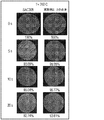
図1A及び1Bは、96.5重量%のスズ、3.0%の銀及び0.5重量%の銅を含む先行技術のSAC305合金の表面の領域の走査型電子顕微鏡(「SEM」)顕微鏡写真を示す。図2A及び図2Bは、表2に示す実施例2.3の組成物による合金の表面の領域のSEM顕微鏡写真を示す。図1A及び2Aは、鋳放しの合金を示し、一方、図1B及び図2Bは、125℃の温度で24時間の時効後の合金を示す。SEM顕微鏡写真から分かるように、高温での時効中のSAC305(図1A及び図1Bに示される)の結晶粒構造は粗大である。対照的に、実施例2.3の合金は、125℃での時効中に、そのより微細でより均一な結晶粒構造を維持する(図2Aと図2Bとの比較)。微細構造はAg3Sn及びCu6Sn5沈殿物を含有し、ビスマス及びアンチモンは各々、スズマトリックス中に溶解し、固溶体強化をもたらす。コバルトは微量合金元素として作用して、微細構造を精密化する。微細化されたAg3Sn及びCu6Sn5沈殿物及び固溶体の強化は、高温での時効中に微細構造を安定化させる。 Figures 1A and 1B are scanning electron microscope (“SEM”) microscopes in the surface region of a prior art SAC305 alloy containing 96.5% by weight tin, 3.0% silver and 0.5% by weight copper. The photograph is shown. 2A and 2B show SEM micrographs of the surface region of the alloy with the composition of Example 2.3 shown in Table 2. 1A and 2A show as-cast alloys, while FIGS. 1B and 2B show alloys after aging for 24 hours at a temperature of 125 ° C. As can be seen from the SEM micrograph, the grain structure of SAC305 (shown in FIGS. 1A and 1B) during aging at high temperature is coarse. In contrast, the alloy of Example 2.3 maintains its finer and more uniform grain structure during aging at 125 ° C. (comparison between FIGS. 2A and 2B). The microstructure contains Ag 3 Sn and Cu 6 Sn 5 precipitates, with bismuth and antimony each dissolving in the tin matrix, resulting in solid solution strengthening. Cobalt acts as a trace alloy element to refine the microstructure. Reinforcement of the micronized Ag 3 Sn and Cu 6 Sn 5 precipitates and solid solutions stabilizes the microstructure during aging at high temperatures.
図3〜図6に示されるように、はんだ合金の溶融特性を、示差走査熱量測定(「DSC」)によって決定した。はんだ合金のための過冷却(すなわち、加熱開始温度と冷却開始温度との間の温度差)を測定した。過冷却は、結晶の沈殿が自発性ではないが、活性化エネルギーを必要とするために生じる。図3は、96.5重量%のスズ、3.0%の銀及び0.5重量%の銅を含む先行技術のSAC305合金のDSC曲線を示す。図4、5、及び6は、それぞれ、表2に示す実施例2.2、2.3、及び2.5の組成物による合金のDSC曲線を示す。加えて、DSC分析からのデータを表3に示す。 As shown in FIGS. 3 to 6, the melting characteristics of the solder alloy were determined by differential scanning calorimetry (“DSC”). Supercooling for the solder alloy (ie, the temperature difference between the heating start temperature and the cooling start temperature) was measured. Supercooling occurs because the precipitation of crystals is not spontaneous, but requires activation energy. FIG. 3 shows the DSC curve of a prior art SAC305 alloy containing 96.5% by weight tin, 3.0% silver and 0.5% by weight copper. FIGS. 4, 5 and 6 show the DSC curves of the alloys according to the compositions of Examples 2.2, 2.3 and 2.5 shown in Table 2, respectively. In addition, the data from the DSC analysis are shown in Table 3.
スズ−銀−銅(Sn−Ag−Cu)はんだの高過冷却挙動は、溶融したスズはんだが固化するのが困難であることを示す。高過冷却は、液相から固相を核形成するのが困難であることに起因する。大きな過冷却は、スズデンドライト、共晶微細構造、主要な金属間化合物(Ag3Sn、Cu6Sn5)などの微細構造の特徴に影響を与え得、はんだの機械的特性に影響を与える。このような過冷却は、はんだ接合部の信頼性に深刻な影響を与える場合があり、接合部が異なる時間に凝固するという不都合な状況を引き起こす可能性がある。これは、凝固した接合部に応力集中をもたらし、機械的故障を引き起こす可能性がある。 The high supercooling behavior of tin-silver-copper (Sn-Ag-Cu) solder indicates that the molten tin solder is difficult to solidify. High supercooling is due to the difficulty of nucleating a solid phase from the liquid phase. Large supercooling can affect microstructural features such as tin dendrites, eutectic microstructures, major intermetallic compounds (Ag 3 Sn, Cu 6 Sn 5 ) and affect the mechanical properties of solders. Such supercooling can seriously affect the reliability of the solder joints and can cause the inconvenient situation that the joints solidify at different times. This causes stress concentration in the solidified joint and can cause mechanical failure.
図3を図4〜6と比較することによって、及び表3を再検討することによって分かるように、いくつかの例示的な合金は、先行技術のSAC305合金と比較して、過冷却の顕著な低減を呈する。例えば、先行技術のSAC305合金については、加熱開始(T1)は217℃であり、冷却開始(T2)は197℃であり、20℃の過冷却(ΔΤ)を提供している。実施例2.3の合金については、T1はおよそ212℃であり、T2はおよそ205.6℃であり、6℃を超える過冷却(ΔΤ)をも提供している。実施例2.5の合金の過冷却は、およそ5.5℃で更に低い。 As can be seen by comparing FIG. 3 with FIGS. 4-6 and by reviewing Table 3, some exemplary alloys are markedly supercooled compared to the prior art SAC305 alloys. Presents a reduction. For example, for the prior art SAC305 alloy, the heating start (T 1 ) is 217 ° C and the cooling start (T 2 ) is 197 ° C, providing a 20 ° C supercooling (ΔΤ). For the alloy of Example 2.3, T 1 is about 212 ° C and T 2 is about 205.6 ° C, which also provides supercooling (ΔΤ) above 6 ° C. The supercooling of the alloy of Example 2.5 is even lower at about 5.5 ° C.
図7A及び7Bは、先行技術のSAC305合金、実施例2.3の合金、及び実施例2.5の合金の間の濡れ時間(図7A)及び最大濡れ力(図7B)の比較を示す。濡れ実験を、IPC(Association Connecting Electronics Industries)標準のIPC−TM−650に従って行った。この標準は、合計濡れ時間及び最大濡れ力を決定することを伴う濡れ平衡試験を伴う。より短い濡れ時間は、より高い濡れ性に対応する。より短い濡れ時間及びより高い濡れ力は、より良好な濡れ性能を反映し、所与のはんだ付けプロセスの下での広がり及びフィレット形成と相関する。図7A及び7Bは、実施例2.3及び2.5の合金の濡れ特性が、先行技術のSAC305合金よりも良好である(又はそれに匹敵する最小値である)ことを示す。 7A and 7B show a comparison of the wetting time (FIG. 7A) and maximum wetting force (FIG. 7B) between the prior art SAC305 alloy, the alloy of Example 2.3, and the alloy of Example 2.5. Wetting experiments were performed according to IPC-TM-650, an IPC (Association Connecting Electronics) standard. This standard involves a wet equilibrium test that involves determining the total wetting time and maximum wetting force. Shorter wetting times correspond to higher wettability. Shorter wetting times and higher wetting forces reflect better wetting performance and correlate with spread and fillet formation under a given soldering process. 7A and 7B show that the wettability of the alloys of Examples 2.3 and 2.5 is better (or comparable to the minimum) than the prior art SAC305 alloy.
はんだの濡れ性能は、広がり率及び広がり性に関して表現され得る。広がり面積は、はんだ付けパッド基板上のはんだがどの程度であるかを示し、広がり率として示され得る。広がり試験を、IPC(IPC J−STD−004B、TM2.4.46)及びJIS Z 3197標準に従って行った。広がり率及び広がり性を、裸銅(Cu)、水溶性プリフラックス(OSP)コーティングされた銅、及び無電解ニッケル置換金(ENIG)めっき銅の3つの異なる基板について調査した。はんだ合金(円形プリフォーム)を、フラックスを使用して試験対象基板上に溶融させた。濡れ面積は、試験前及び試験後の光学顕微鏡を使用して測定した。広がり率は、リフロー/溶融後の濡れ面積をリフロー/溶融前の濡れ面積で割ることによって計算される。はんだ高さを測定して広がり性(又は広がり係数)を計算した。広がり性は、以下の式を使用して計算した、式中、SR=広がり性、D=はんだの直径(球形であると想定される)、H=広がったはんだの高さ、V=はんだの体積(g/cm3)(試験したはんだの質量及び密度から推定): Wetting performance of solder can be expressed in terms of spreadability and spreadability. The spread area indicates how much solder is on the soldering pad substrate and can be expressed as a spread ratio. Spread tests were performed according to IPC (IPC J-STD-004B, TM2.4.46) and JIS Z 3197 standards. Spreadability and spreadability were investigated for three different substrates: bare copper (Cu), water-soluble preflux (OSP) coated copper, and electroless nickel-substituted gold (ENIG) plated copper. A solder alloy (circular preform) was melted onto the substrate under test using flux. Wet area was measured using a light microscope before and after the test. The spread rate is calculated by dividing the wet area after reflow / melting by the wet area before reflow / melting. The spreadability (or spread coefficient) was calculated by measuring the solder height. Spreadability was calculated using the following formula: SR = spreadability, D = solder diameter (assumed to be spherical), H = spread solder height, V = solder Volume (g / cm 3 ) (estimated from the mass and density of the tested solder):
![]()
![]()
図8Aは、2つの異なる温度(260℃及び300℃)での裸銅基板上での先行技術のSAC合金と比較した、実施例2.3の合金の広がり率の比較を示す。図8Bは、2つの異なる温度(260℃及び300℃)での先行技術のSAC合金と比較した、実施例2.3の合金の広がり性の比較を示す。 FIG. 8A shows a comparison of alloy spread rates of Example 2.3 compared to prior art SAC alloys on bare copper substrates at two different temperatures (260 ° C and 300 ° C). FIG. 8B shows a comparison of the spreadability of the alloy of Example 2.3 compared to the prior art SAC alloys at two different temperatures (260 ° C and 300 ° C).
図9Aは、255℃での3つの異なる銅基板(OSP、裸銅、及びENIG)上での実施例2.3の合金の広がり率の比較を示す。図9Bは、255℃での3つの異なる銅基板(OSP、裸銅、及びENIG)上での実施例2,3の合金の広がり性の比較を示す。 FIG. 9A shows a comparison of the spread rates of the alloys of Example 2.3 on three different copper substrates (OSP, bare copper, and ENIG) at 255 ° C. FIG. 9B shows a comparison of the spreadability of the alloys of Examples 2 and 3 on three different copper substrates (OSP, bare copper, and ENIG) at 255 ° C.
図10A、10B、11A、及び11Bは、260℃(図10A及び11A)及び280℃(図10B及び図11B)での先行技術のSAC305合金と実施例2.3の合金(合金−B)との間の銅溶解速度の比較を示す。これらの図に見られるように、銅溶解速度は、先行技術のSAC305合金と比較して、実施例2.3の合金ではより遅くなる。銅溶解試験は、洗浄し、脱脂し、酸溶液中で洗浄し、すすぎ洗いし、乾燥させた純銅線を用いて行った。試験は、260℃及び280℃の2つの温度で実施した。銅ワイヤを、5秒、10秒、及び20秒間、溶融はんだに曝露した。銅ワイヤの断面を、面積測定及び分析の実行を含め、光学顕微鏡法により分析した。 10A, 10B, 11A, and 11B are the SAC305 alloy of the prior art at 260 ° C. (FIGS. 10A and 11A) and 280 ° C. (FIGS. 10B and 11B) and the alloy of Example 2.3 (alloy-B). A comparison of copper melting rates between the two is shown. As can be seen in these figures, the copper melting rate is slower in the alloy of Example 2.3 as compared to the prior art SAC305 alloy. The copper dissolution test was performed using pure copper wire washed, degreased, washed in acid solution, rinsed and dried. The test was carried out at two temperatures, 260 ° C and 280 ° C. The copper wire was exposed to molten solder for 5 seconds, 10 seconds, and 20 seconds. The cross section of the copper wire was analyzed by light microscopy, including area measurements and analysis.
図12Aは、先行技術のSAC305合金と比較した、実施例2.3の合金の硬度値を示す。棒グラフから分かるように、実施例2.3の合金の硬度は、先行技術のSAC305合金の硬度よりも高い。更に、実施例2.3の合金は、鋳放し、150℃で144時間の時効後、及び150℃で720時間の時効後の硬度試験の結果を示す図12Bに示すように、先行技術のSAC305合金とは対照的に、その硬度を保つ。 FIG. 12A shows the hardness values of the alloy of Example 2.3 compared to the prior art SAC305 alloy. As can be seen from the bar graph, the hardness of the alloy of Example 2.3 is higher than the hardness of the SAC305 alloy of the prior art. Further, the alloy of Example 2.3 was cast, and as shown in FIG. 12B showing the results of hardness tests after aging at 150 ° C. for 144 hours and after aging at 150 ° C. for 720 hours, the prior art SAC305 In contrast to alloys, it retains its hardness.
本開示による合金の熱膨張係数(CTE)も測定した。はんだとその下層の基板とのCTEの不一致は、繰り返し荷重中の疲労破壊をもたらし得る。CTEの不一致が増すと、剪断ひずみも大きくなり、構成要素の熱サイクル寿命を減少させる。CTEの不一致に起因して応力集中部位にひび割れが始まり、伝播する場合がある。はんだ接合部のひび割れは、はんだとその下層の基板とのCTEの差を低減することによって低減され得る。表4は、先行技術のSAC305合金と比較し、下層の例示的な基板のCTEを参照した、本開示による合金のCTEを示す。 The coefficient of thermal expansion (CTE) of the alloy according to the present disclosure was also measured. A CTE mismatch between the solder and the underlying substrate can result in fatigue fracture during repeated loading. As the CTE discrepancy increases, so does the shear strain, which reduces the thermal cycle life of the components. Cracks may begin and propagate in stress-concentrated areas due to CTE discrepancies. Cracks in the solder joint can be reduced by reducing the difference in CTE between the solder and the underlying substrate. Table 4 shows the CTEs of the alloys according to the present disclosure, with reference to the CTEs of the underlying exemplary substrates compared to the prior art SAC305 alloys.
先行技術のSAC305合金と比較した、本開示による例示的な合金(実施例2.3の合金)の引張応力−ひずみグラフを図13に示す。鋳造はんだを機械加工し、サイズ100mm×6mm×3mmの矩形片に切断した。試料を、150℃で最大720時間、等温時効した。引張試験を、10−2s−1のひずみ速度で室温で実施した。合金の極限引張強度及び降伏強度を表5に示す。実施例2.3の合金に示される引張強度の有意な改善は、ビスマスの添加及び固溶体強化の効果に起因し得る。実施例2.3の合金はまた、先行技術のSAC305合金よりも延性が高いことを示している。150℃での時効後の、実施例2.3の合金及び先行技術のSAC305合金の引張強度特性を図14に示す。実施例2.3の合金及び先行技術のSAC305合金の両方とも、高温での時効後の極限引張強度の低減を示しているが、この低減は、引張強度の約42%の低減を呈する先行技術のSAC305合金に関してかなり顕著である。 FIG. 13 shows a tensile stress-strain graph of an exemplary alloy (alloy of Example 2.3) according to the present disclosure compared to the prior art SAC305 alloy. The cast solder was machined and cut into rectangular pieces measuring 100 mm x 6 mm x 3 mm. Samples were isothermally aged at 150 ° C. for up to 720 hours. The tensile test was performed at room temperature strain rate of 10 -2 s -1. Table 5 shows the ultimate tensile strength and yield strength of the alloy. The significant improvement in tensile strength shown in the alloy of Example 2.3 may be due to the effects of the addition of bismuth and the strengthening of the solid solution. The alloy of Example 2.3 has also been shown to be more ductile than the prior art SAC305 alloy. The tensile strength characteristics of the alloy of Example 2.3 and the prior art SAC305 alloy after aging at 150 ° C. are shown in FIG. Both the alloy of Example 2.3 and the prior art SAC305 alloy show a reduction in ultimate tensile strength after aging at high temperatures, which prior art exhibits a reduction of approximately 42% in tensile strength. It is quite remarkable with respect to the SAC305 alloy of.
クリープ変形は、高い相同温度の関わりによる、超小型電子パッケージング内のはんだ接合部の重故障モードである。はんだは、パッケージ内のチップと他の層との異なる熱膨張係数(CTE)に起因する熱機械的応力を経験する。これらの応力は、長期間の使用で塑性変形を引き起こし得る。はんだ合金は、室温でもクリープ変形を受ける場合がある。実際の寿命用途では、電子モジュールは、−40℃〜+125℃の温度範囲で動作し得、これは、0.48〜0.87Tm(はんだの融解温度の割合)の範囲である。応力下のデバイスにとって、これは急速クリープ変形の範囲である。このように、鉛フリーはんだにおけるクリープ変形を完全に理解することは、電子パッケージング産業にとって重要な懸念事項である。鋳造はんだを機械加工し、サイズ120mm×6mm×3mmの矩形片に切断した。試料を、150℃で最大144時間、等温エージングした。クリープ試験を10MPaの応力レベルで室温にて実施した。図15に示すように、本開示による実施例2.3の合金は、先行技術のSAC305合金と比較して優れたクリープ抵抗を示す。実施例2.3の合金によって呈されるクリープ抵抗は、微細構造を微細化するための微細合金の添加、並びに固溶体及び沈殿硬化などの強化機構に起因し得る。 Creep deformation is a major failure mode of solder joints in ultra-small electronic packaging due to the involvement of high homologous temperatures. Solder experiences thermomechanical stresses due to the different coefficients of thermal expansion (CTE) between the chips in the package and the other layers. These stresses can cause plastic deformation with long-term use. Solder alloys may undergo creep deformation even at room temperature. In actual life applications, electronic modules can operate in the temperature range of −40 ° C. to + 125 ° C., which is in the range of 0.48 to 0.87 Tm (percentage of solder melting temperature). For stressed devices, this is a range of rapid creep deformation. Thus, a complete understanding of creep deformation in lead-free solder is an important concern for the electronic packaging industry. The cast solder was machined and cut into rectangular pieces measuring 120 mm x 6 mm x 3 mm. Samples were isothermally aged at 150 ° C. for up to 144 hours. The creep test was performed at room temperature with a stress level of 10 MPa. As shown in FIG. 15, the alloy of Example 2.3 according to the present disclosure exhibits superior creep resistance as compared to the prior art SAC305 alloy. The creep resistance exhibited by the alloy of Example 2.3 may be due to the addition of the fine alloy to refine the microstructure and the strengthening mechanism such as solid solution and precipitation hardening.
はんだ付け操作中に、固体基板からの材料が溶解し、はんだと混合され、金属間化合物(IMC)が形成されることを可能にする。薄く、連続的で、かつ均一なIMC層は、良好な結合のために重要である傾向がある。IMCなしでは、接合において冶金相互作用が生じないため、はんだ/導体接合部は弱くなる傾向がある。しかしながら、厚いIMC層は脆性であり得るため、境界面の厚いIMC層は、はんだ接合部の信頼性を低下させ得る。露出時間及び温度に応じて、はんだとOSP基板との間に形成されたIMC層を検査した。はんだ合金をOSP基板上で溶融させ、フラックスを使用してElectrovert OmniExcel 7 Zone Reflowオーブン内でリフローした。次いで、はんだ合金試料を最大1440時間、150℃の高温に曝露した。IMC層を異なる時効期間で評価した。 During the soldering operation, the material from the solid substrate can be melted and mixed with the solder to form an intermetallic compound (IMC). A thin, continuous, and uniform IMC layer tends to be important for good bonding. Without the IMC, the solder / conductor joints tend to be weak because no metallurgical interactions occur in the joints. However, since a thick IMC layer can be brittle, a thick IMC layer at the interface can reduce the reliability of the solder joint. The IMC layer formed between the solder and the OSP substrate was inspected according to the exposure time and temperature. The solder alloy was melted on an OSP substrate and reflowed in an Electrovert OmniExcel 7 Zone Reflow oven using flux. The solder alloy sample was then exposed to a high temperature of 150 ° C. for up to 1440 hours. The IMC layer was evaluated with different aging periods.
図16A及び図16Bは、150℃で最大1440時間の時効後の、実施例2.3の合金とSAC305合金とのIMC層成長の比較を示す。これらの図に見られるように、実施例2.3の合金及びSAC305合金の両方がIMC層成長を呈している。しかしながら、SAC305合金は、カーケンダルボイドの存在によって示されるように、脆性の兆候を示している(例えば、720時間の時効後)。両合金とも、はんだと銅基板との間の境界にCu6Sn5層及びCu3Sn層の形成を示している。図17は、時効時間の関数としての合計IMC厚さを示す。図17に示すように、SAC305合金のIMC層は、実施例2.3の合金よりもはるかに厚い。微細構造を微細化するための微細合金の添加は、拡散を制限し、それにより、合計IMC成長も制限し得る。実施例2.3の合金のIMC厚さが小さいと、実施例2.3の合金が高温での長寿命用途に好適になる可能性が高い。図18は、時効時間に応じた合計Cu3Sn厚さを示す。両合金とも、Cu6Sn5とCu基板との間の境界面に、Cu3Snの新しいIMC層が形成される。実施例2.3の合金では、微細合金の添加によって、Cu3Snの成長が抑制され、カーケンダルボイドの形成が制限され得る。 16A and 16B show a comparison of IMC layer growth between the alloy of Example 2.3 and the SAC305 alloy after aging at 150 ° C. for up to 1440 hours. As can be seen in these figures, both the alloy of Example 2.3 and the SAC305 alloy exhibit IMC layer growth. However, the SAC305 alloy shows signs of brittleness (eg, after 720 hours of aging), as indicated by the presence of Kirkendal voids. Both alloys show the formation of Cu 6 Sn 5 layers and Cu 3 Sn layers at the boundary between the solder and the copper substrate. FIG. 17 shows the total IMC thickness as a function of aging time. As shown in FIG. 17, the IMC layer of the SAC305 alloy is much thicker than the alloy of Example 2.3. The addition of microalloys to refine the microstructure can limit diffusion and thereby total IMC growth. If the IMC thickness of the alloy of Example 2.3 is small, it is likely that the alloy of Example 2.3 will be suitable for long life applications at high temperatures. FIG. 18 shows the total Cu 3 Sn thickness according to the aging time. In both alloys, a new IMC layer of Cu 3 Sn is formed on the interface between the Cu 6 Sn 5 and the Cu substrate. In the alloy of Example 2.3, the addition of the fine alloy can suppress the growth of Cu 3 Sn and limit the formation of Kirkendal voids.
本明細書に記載される要素のいくつかは、任意選択的なものとして明示的に識別されているが、他の要素はこのように識別されていない。そのように識別されない場合であっても、いくつかの実施形態では、これらの他の要素のいくつかは、必須のものとして解釈されることを意図するものではなく、当業者には任意のものとして理解されるであろう。 Some of the elements described herein have been explicitly identified as optional, while others have not. Even if not so identified, in some embodiments, some of these other elements are not intended to be construed as mandatory and are optional to those skilled in the art. Will be understood as.
本開示は、特定の実装形態を参照して記載されているが、本方法及び/又はシステムの範囲から逸脱することなく、様々な変更がなされてもよく、等価物が代用されてもよいことが当業者には理解されるであろう。加えて、その範囲から逸脱することなく、本開示の教示に特定の状況又は材料を適合させるために、多くの修正がなされてもよい。例えば、開示される実施例のシステム、ブロック、及び/又は他の構成要素は、組み合わされ、分割され、再配置され、かつ/ないしは他の方法で修正されてもよい。したがって、本開示は、開示される特定の実装形態に限定されない。代わりに、本開示は、文言上及び均等論上の両方において、添付の「特許請求の範囲」内の全ての実装形態を含む。 Although the present disclosure is described with reference to a particular implementation, various modifications may be made and equivalents may be substituted without departing from the scope of the method and / or system. Will be understood by those skilled in the art. In addition, many modifications may be made to adapt a particular situation or material to the teachings of the present disclosure without departing from that scope. For example, the disclosed embodiment systems, blocks, and / or other components may be combined, divided, rearranged, and / or modified in other ways. Therefore, the present disclosure is not limited to the specific implementations disclosed. Instead, the present disclosure includes all implementations within the appended claims, both literally and doctrine of equivalents.
Claims (11)
2.0〜2.8重量%の銀と、
0.2〜1.2重量%の銅と、
0.0〜5.0重量%のビスマスと、
0.001〜0.2重量%のコバルトと、
0.0〜0.09重量%のアンチモンと、
残部のスズと、を任意の不可避不純物と共に含む、鉛フリーはんだ合金。 It is a lead-free solder alloy
From 2.0 to 2.8% by weight of silver,
With 0.2-1.2 wt% copper,
With 0.0-5.0% by weight bismuth,
0.001-0.2 wt% cobalt and
0.0-0.09% by weight of antimony,
A lead-free solder alloy containing the balance of tin, along with any unavoidable impurities.
Applications Claiming Priority (5)
| Application Number | Priority Date | Filing Date | Title |
|---|---|---|---|
| US201762583934P | 2017-11-09 | 2017-11-09 | |
| US62/583,934 | 2017-11-09 | ||
| US16/022,337 | 2018-06-28 | ||
| US16/022,337 US11577343B2 (en) | 2017-11-09 | 2018-06-28 | Low-silver alternative to standard SAC alloys for high reliability applications |
| PCT/US2018/058463 WO2019094242A1 (en) | 2017-11-09 | 2018-10-31 | Low-silver tin based alternative solder alloy to standard sac alloys for high reliability applications |
Publications (2)
| Publication Number | Publication Date |
|---|---|
| JP2021502259A true JP2021502259A (en) | 2021-01-28 |
| JP2021502259A5 JP2021502259A5 (en) | 2021-12-09 |
Family
ID=66326662
Family Applications (1)
| Application Number | Title | Priority Date | Filing Date |
|---|---|---|---|
| JP2020544348A Pending JP2021502259A (en) | 2017-11-09 | 2018-10-31 | Low silver tin alternative solder alloy to standard SAC alloy for high reliability applications |
Country Status (8)
| Country | Link |
|---|---|
| US (1) | US11577343B2 (en) |
| EP (2) | EP4299238A3 (en) |
| JP (1) | JP2021502259A (en) |
| KR (1) | KR20200089273A (en) |
| CN (1) | CN111542624A (en) |
| SG (1) | SG11202004067UA (en) |
| TW (1) | TWI782134B (en) |
| WO (1) | WO2019094242A1 (en) |
Families Citing this family (2)
| Publication number | Priority date | Publication date | Assignee | Title |
|---|---|---|---|---|
| KR102187085B1 (en) * | 2019-01-24 | 2020-12-04 | 주식회사 경동엠텍 | lead-free solder composition for high-temperature and vibrational circumstance and manufacturing method thereof |
| TWI814081B (en) | 2019-09-02 | 2023-09-01 | 美商阿爾發金屬化工公司 | High temperature ultra-high reliability alloys, manufacturing method thereof, and applications thereof |
Citations (6)
| Publication number | Priority date | Publication date | Assignee | Title |
|---|---|---|---|---|
| JP2002246742A (en) * | 2000-12-11 | 2002-08-30 | Nec Toyama Ltd | Solder, surface treatment method of printed-wiring board using the same, and packaging method of electronic component using the surface treatment method |
| JP2004141910A (en) * | 2002-10-23 | 2004-05-20 | Senju Metal Ind Co Ltd | Lead-free solder alloy |
| WO2014002283A1 (en) * | 2012-06-30 | 2014-01-03 | 千住金属工業株式会社 | Lead-free solder ball |
| JP2014027122A (en) * | 2012-07-27 | 2014-02-06 | Nippon Steel Sumikin Materials Co Ltd | Lead-free solder bump bonding structure |
| JP2015020182A (en) * | 2013-07-17 | 2015-02-02 | ハリマ化成株式会社 | Solder composition, solder paste, and electronic circuit board |
| JP2017162960A (en) * | 2016-03-09 | 2017-09-14 | 株式会社タムラ製作所 | Bonding method of electronic component, and solder composition |
Family Cites Families (23)
| Publication number | Priority date | Publication date | Assignee | Title |
|---|---|---|---|---|
| US6176947B1 (en) | 1998-12-31 | 2001-01-23 | H-Technologies Group, Incorporated | Lead-free solders |
| SG98429A1 (en) * | 1999-10-12 | 2003-09-19 | Singapore Asahi Chemical & Solder Ind Pte Ltd | Lead-free solders |
| US8216395B2 (en) * | 2001-06-28 | 2012-07-10 | Senju Metal Industry Co., Ltd. | Lead-free solder alloy |
| GB2419137A (en) * | 2004-10-15 | 2006-04-19 | Alpha Fry Ltd | Solder alloy |
| EP1889684B1 (en) * | 2005-06-03 | 2016-03-30 | Senju Metal Industry Co., Ltd. | Lead-free solder alloy |
| CN100453244C (en) * | 2005-12-16 | 2009-01-21 | 浙江亚通焊材有限公司 | Lead les tin solder |
| JP5024380B2 (en) * | 2007-07-13 | 2012-09-12 | 千住金属工業株式会社 | Lead-free solder for in-vehicle mounting and in-vehicle electronic circuit |
| DE102009039355A1 (en) * | 2009-08-29 | 2011-03-24 | Umicore Ag & Co. Kg | solder alloy |
| JP5722302B2 (en) * | 2010-02-16 | 2015-05-20 | 株式会社タムラ製作所 | Lead-free solder alloy, solder paste using this, and mounted product |
| JP2011251310A (en) | 2010-06-02 | 2011-12-15 | Nippon Genma:Kk | Lead-free solder alloy |
| CN102666002B (en) * | 2010-08-18 | 2014-09-10 | 新日铁住金高新材料株式会社 | Solder ball for semiconductor mounting and electronic member |
| WO2012127642A1 (en) * | 2011-03-23 | 2012-09-27 | 千住金属工業株式会社 | Lead-free solder alloy |
| KR20160011242A (en) | 2012-10-09 | 2016-01-29 | 알파 메탈즈, 인코포레이티드 | Lead-free and antimony-free tin solder reliable at high temperatures |
| JP2015077601A (en) | 2013-04-02 | 2015-04-23 | 千住金属工業株式会社 | Lead-free solder alloy |
| US9559543B2 (en) * | 2013-07-19 | 2017-01-31 | Apple Inc. | Adaptive effective C-rate charging of batteries |
| CN105189027B (en) * | 2013-09-11 | 2018-06-29 | 千住金属工业株式会社 | Lead-free solder, Lead-free solder ball, the solder joints for having used the lead-free solder and the semiconductor circuit with the solder joints |
| JP2016019992A (en) | 2014-07-14 | 2016-02-04 | 株式会社日本スペリア社 | Aluminium soldering and solder joint |
| JP5723056B1 (en) * | 2014-12-15 | 2015-05-27 | ハリマ化成株式会社 | Solder alloy, solder paste and electronic circuit board |
| US20160279741A1 (en) | 2015-03-24 | 2016-09-29 | Tamura Corporation | Lead-free solder alloy, electronic circuit board, and electronic control device |
| WO2017018167A1 (en) * | 2015-07-24 | 2017-02-02 | ハリマ化成株式会社 | Solder alloy, solder paste, and electronic circuit board |
| US10195698B2 (en) | 2015-09-03 | 2019-02-05 | AIM Metals & Alloys Inc. | Lead-free high reliability solder alloys |
| BR112018068596A2 (en) * | 2016-03-22 | 2019-02-12 | Tamura Corporation | Lead-free solder alloy, flux composition, solder paste composition, electronic circuit board, and electronic controller |
| US20180102464A1 (en) * | 2016-10-06 | 2018-04-12 | Alpha Assembly Solutions Inc. | Advanced Solder Alloys For Electronic Interconnects |
-
2018
- 2018-06-28 US US16/022,337 patent/US11577343B2/en active Active
- 2018-10-31 EP EP23202671.6A patent/EP4299238A3/en active Pending
- 2018-10-31 KR KR1020207015369A patent/KR20200089273A/en active IP Right Grant
- 2018-10-31 SG SG11202004067UA patent/SG11202004067UA/en unknown
- 2018-10-31 JP JP2020544348A patent/JP2021502259A/en active Pending
- 2018-10-31 EP EP18804799.7A patent/EP3707285B1/en active Active
- 2018-10-31 WO PCT/US2018/058463 patent/WO2019094242A1/en unknown
- 2018-10-31 CN CN201880072408.6A patent/CN111542624A/en active Pending
- 2018-11-08 TW TW107139607A patent/TWI782134B/en active
Patent Citations (6)
| Publication number | Priority date | Publication date | Assignee | Title |
|---|---|---|---|---|
| JP2002246742A (en) * | 2000-12-11 | 2002-08-30 | Nec Toyama Ltd | Solder, surface treatment method of printed-wiring board using the same, and packaging method of electronic component using the surface treatment method |
| JP2004141910A (en) * | 2002-10-23 | 2004-05-20 | Senju Metal Ind Co Ltd | Lead-free solder alloy |
| WO2014002283A1 (en) * | 2012-06-30 | 2014-01-03 | 千住金属工業株式会社 | Lead-free solder ball |
| JP2014027122A (en) * | 2012-07-27 | 2014-02-06 | Nippon Steel Sumikin Materials Co Ltd | Lead-free solder bump bonding structure |
| JP2015020182A (en) * | 2013-07-17 | 2015-02-02 | ハリマ化成株式会社 | Solder composition, solder paste, and electronic circuit board |
| JP2017162960A (en) * | 2016-03-09 | 2017-09-14 | 株式会社タムラ製作所 | Bonding method of electronic component, and solder composition |
Also Published As
| Publication number | Publication date |
|---|---|
| EP4299238A2 (en) | 2024-01-03 |
| US11577343B2 (en) | 2023-02-14 |
| US20190134758A1 (en) | 2019-05-09 |
| EP4299238A3 (en) | 2024-03-27 |
| EP3707285B1 (en) | 2023-11-29 |
| KR20200089273A (en) | 2020-07-24 |
| CN111542624A (en) | 2020-08-14 |
| TWI782134B (en) | 2022-11-01 |
| WO2019094242A1 (en) | 2019-05-16 |
| SG11202004067UA (en) | 2020-05-28 |
| EP3707285A1 (en) | 2020-09-16 |
| TW201923103A (en) | 2019-06-16 |
Similar Documents
| Publication | Publication Date | Title |
|---|---|---|
| Ren et al. | Alloying influences on low melt temperature SnZn and SnBi solder alloys for electronic interconnections | |
| KR101339025B1 (en) | Solder alloy | |
| US20230340642A1 (en) | High reliability lead-free solder alloy for electronic applications in extreme environments | |
| JP2021502259A (en) | Low silver tin alternative solder alloy to standard SAC alloy for high reliability applications | |
| JP6887183B1 (en) | Solder alloys and molded solders | |
| JP7273049B2 (en) | Cost-effective lead-free solder alloy for electronic applications | |
| JP4425738B2 (en) | Lead-free solder alloy, lead-free solder alloy manufacturing method, mounting structure, mounting method, lead-free fuse alloy, lead-free fuse alloy manufacturing method, plate-shaped fuse, lead-free alloy and lead-free alloy manufacturing method | |
| JP5633812B2 (en) | Au-Sn alloy solder | |
| Islam | Processing and characterization of zinc-silver based high temperature solder alloys | |
| JP2006000925A (en) | Lead-free solder alloy and producing method thereof |
Legal Events
| Date | Code | Title | Description |
|---|---|---|---|
| RD03 | Notification of appointment of power of attorney |
Free format text: JAPANESE INTERMEDIATE CODE: A7423 Effective date: 20200630 |
|
| RD04 | Notification of resignation of power of attorney |
Free format text: JAPANESE INTERMEDIATE CODE: A7424 Effective date: 20201007 |
|
| A521 | Request for written amendment filed |
Free format text: JAPANESE INTERMEDIATE CODE: A523 Effective date: 20211027 |
|
| A621 | Written request for application examination |
Free format text: JAPANESE INTERMEDIATE CODE: A621 Effective date: 20211027 |
|
| A711 | Notification of change in applicant |
Free format text: JAPANESE INTERMEDIATE CODE: A711 Effective date: 20220204 |
|
| A977 | Report on retrieval |
Free format text: JAPANESE INTERMEDIATE CODE: A971007 Effective date: 20221025 |
|
| A131 | Notification of reasons for refusal |
Free format text: JAPANESE INTERMEDIATE CODE: A131 Effective date: 20221101 |
|
| A601 | Written request for extension of time |
Free format text: JAPANESE INTERMEDIATE CODE: A601 Effective date: 20230131 |
|
| A02 | Decision of refusal |
Free format text: JAPANESE INTERMEDIATE CODE: A02 Effective date: 20230530 |