JP2021190841A - Directional coupler - Google Patents
Directional coupler Download PDFInfo
- Publication number
- JP2021190841A JP2021190841A JP2020094470A JP2020094470A JP2021190841A JP 2021190841 A JP2021190841 A JP 2021190841A JP 2020094470 A JP2020094470 A JP 2020094470A JP 2020094470 A JP2020094470 A JP 2020094470A JP 2021190841 A JP2021190841 A JP 2021190841A
- Authority
- JP
- Japan
- Prior art keywords
- filter
- switch
- filters
- output terminal
- directional coupler
- Prior art date
- Legal status (The legal status is an assumption and is not a legal conclusion. Google has not performed a legal analysis and makes no representation as to the accuracy of the status listed.)
- Pending
Links
Images


Classifications
-
- H—ELECTRICITY
- H03—ELECTRONIC CIRCUITRY
- H03H—IMPEDANCE NETWORKS, e.g. RESONANT CIRCUITS; RESONATORS
- H03H7/00—Multiple-port networks comprising only passive electrical elements as network components
- H03H7/38—Impedance-matching networks
- H03H7/40—Automatic matching of load impedance to source impedance
-
- H—ELECTRICITY
- H01—ELECTRIC ELEMENTS
- H01P—WAVEGUIDES; RESONATORS, LINES, OR OTHER DEVICES OF THE WAVEGUIDE TYPE
- H01P5/00—Coupling devices of the waveguide type
- H01P5/12—Coupling devices having more than two ports
- H01P5/16—Conjugate devices, i.e. devices having at least one port decoupled from one other port
- H01P5/18—Conjugate devices, i.e. devices having at least one port decoupled from one other port consisting of two coupled guides, e.g. directional couplers
-
- H—ELECTRICITY
- H03—ELECTRONIC CIRCUITRY
- H03H—IMPEDANCE NETWORKS, e.g. RESONANT CIRCUITS; RESONATORS
- H03H7/00—Multiple-port networks comprising only passive electrical elements as network components
- H03H7/01—Frequency selective two-port networks
- H03H7/0123—Frequency selective two-port networks comprising distributed impedance elements together with lumped impedance elements
-
- H—ELECTRICITY
- H03—ELECTRONIC CIRCUITRY
- H03H—IMPEDANCE NETWORKS, e.g. RESONANT CIRCUITS; RESONATORS
- H03H7/00—Multiple-port networks comprising only passive electrical elements as network components
- H03H7/01—Frequency selective two-port networks
- H03H7/06—Frequency selective two-port networks including resistors
-
- H—ELECTRICITY
- H03—ELECTRONIC CIRCUITRY
- H03H—IMPEDANCE NETWORKS, e.g. RESONANT CIRCUITS; RESONATORS
- H03H7/00—Multiple-port networks comprising only passive electrical elements as network components
- H03H7/48—Networks for connecting several sources or loads, working on the same frequency or frequency band, to a common load or source
Abstract
Description
本発明は、方向性結合器に関する。 The present invention relates to a directional coupler.
例えば、特許文献1には、主線路と副線路とを備える方向性結合器が開示されている。方向性結合器の副線路とカップリングポートとの間には、複数のフィルタを含む可変フィルタ回路が接続されている。 For example, Patent Document 1 discloses a directional coupler including a main line and a sub line. A variable filter circuit including a plurality of filters is connected between the sub line of the directional coupler and the coupling port.
フィルタには、例えば、薄膜微細加工を用いた小型で高性能なフィルタを利用することができる。しかしながら、このようなフィルタは、静電気破壊されやすいという問題がある。フィルタが静電気破壊された場合には、フィルタの周波数特性が劣化し、所望の信号を取り出すことができない。 As the filter, for example, a small and high-performance filter using thin film microfabrication can be used. However, such a filter has a problem that it is easily destroyed by static electricity. When the filter is electrostatically destroyed, the frequency characteristics of the filter deteriorate and the desired signal cannot be extracted.
そこで、本発明は、フィルタの周波数特性の劣化を抑制することができる方向性結合器を提供することを目的とする。 Therefore, an object of the present invention is to provide a directional coupler capable of suppressing deterioration of the frequency characteristics of the filter.
本発明の一態様に係る方向性結合器は、主線路と、前記主線路と電磁気的に結合する副線路と、出力端子と、複数のフィルタと、前記複数のフィルタの各々を、前記副線路の一端と前記出力端子とに接続可能であるスイッチ回路と、前記複数のフィルタの各々の両端にそれぞれ直接接続され、対応するフィルタの一端と基準電位との接続及び開放を切替可能である複数のスイッチと、を備える。 In the directional coupler according to one aspect of the present invention, the main line, the sub line electromagnetically coupled to the main line, the output terminal, the plurality of filters, and each of the plurality of filters are connected to the sub line. A switch circuit that can be connected to one end of the filter and the output terminal, and a plurality of switches that are directly connected to both ends of each of the plurality of filters and can switch between the connection and the opening of one end of the corresponding filter and the reference potential. It is equipped with a switch.
また、本発明の別の一態様に係る方向性結合器は、主線路と、前記主線路と電磁気的に結合する副線路と、出力端子と、複数のフィルタと、前記複数のフィルタの各々を、前記副線路の一端と前記出力端子とに接続可能である第1スイッチ回路と、前記複数のフィルタの各々の両端にそれぞれ接続され、対応するフィルタの一端と基準電位との接続及び開放を切替可能である複数の第2スイッチ回路と、を備え、前記複数の第2スイッチ回路は、前記複数のフィルタの1つである対象フィルタを前記第1スイッチ回路が前記副線路の一端と前記出力端子とに接続する場合に、前記対象フィルタの一端と前記基準電位との接続を開放し、かつ、前記対象フィルタ以外のフィルタの一端と前記基準電位とを接続する。 Further, the directional coupler according to another aspect of the present invention includes a main line, a sub line electromagnetically coupled to the main line, an output terminal, a plurality of filters, and each of the plurality of filters. , The first switch circuit that can be connected to one end of the sub line and the output terminal, and the connection and opening of one end of the corresponding filter and the reference potential are switched by being connected to both ends of each of the plurality of filters. The plurality of second switch circuits include a plurality of possible second switch circuits, wherein the target filter, which is one of the plurality of filters, is provided by the first switch circuit at one end of the sub line and the output terminal. When connecting to, the connection between one end of the target filter and the reference potential is opened, and one end of a filter other than the target filter is connected to the reference potential.
本発明に係る方向性結合器によれば、フィルタの周波数特性の劣化を抑制することができる。 According to the directional coupler according to the present invention, deterioration of the frequency characteristics of the filter can be suppressed.
以下では、本発明の実施の形態に係る方向性結合器について、図面を用いて詳細に説明する。なお、以下に説明する実施の形態は、いずれも本発明の一具体例を示すものである。したがって、以下の実施の形態で示される数値、形状、材料、構成要素、構成要素の配置及び接続形態、ステップ、ステップの順序などは、一例であり、本発明を限定する趣旨ではない。よって、以下の実施の形態における構成要素のうち、独立請求項に記載されていない構成要素については、任意の構成要素として説明される。 Hereinafter, the directional coupler according to the embodiment of the present invention will be described in detail with reference to the drawings. In addition, all of the embodiments described below show a specific example of the present invention. Therefore, the numerical values, shapes, materials, components, arrangement and connection forms of components, steps, order of steps, etc. shown in the following embodiments are examples, and are not intended to limit the present invention. Therefore, among the components in the following embodiments, the components not described in the independent claims are described as arbitrary components.
また、各図は、模式図であり、必ずしも厳密に図示されたものではない。したがって、例えば、各図において縮尺などは必ずしも一致しない。また、各図において、実質的に同一の構成については同一の符号を付しており、重複する説明は省略又は簡略化する。 Further, each figure is a schematic view and is not necessarily exactly illustrated. Therefore, for example, the scales and the like do not always match in each figure. Further, in each figure, substantially the same configuration is designated by the same reference numeral, and duplicate description will be omitted or simplified.
また、本明細書において、一致及び等しいなどの要素間の関係性を示す用語、及び、数値範囲は、厳格な意味のみを表す表現ではなく、実質的に同等な範囲、例えば数%程度の差異をも含むことを意味する表現である。 Further, in the present specification, terms indicating relationships between elements such as agreement and equality, and numerical ranges are not expressions that express only strict meanings, but substantially equivalent ranges, for example, differences of about several percent. It is an expression that means to include.
また、本発明の回路構成の説明において、「直接接続される」とは、他の回路素子を介さずに接続端子及び/又は配線導体で直接接続されることを意味する。一方、「接続される」とは、接続端子及び/又は配線導体で直接接続される場合だけでなく、他の回路素子を介して電気的に接続される場合も含む。また、「AとBとの間に接続される」とは、AとBとの間でA及びBの両方に接続されることを意味する。 Further, in the description of the circuit configuration of the present invention, "directly connected" means that the circuit is directly connected by a connection terminal and / or a wiring conductor without using other circuit elements. On the other hand, the term "connected" includes not only the case of being directly connected by a connection terminal and / or a wiring conductor, but also the case of being electrically connected via another circuit element. Further, "connected between A and B" means that both A and B are connected between A and B.
(実施の形態1)
[1−1.構成]
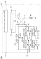
まず、実施の形態1に係る方向性結合器の構成について、図1を用いて説明する。図1は、本実施の形態に係る方向性結合器1の構成を示す図である。
(Embodiment 1)
[1-1. composition]
First, the configuration of the directional coupler according to the first embodiment will be described with reference to FIG. FIG. 1 is a diagram showing a configuration of a directional coupler 1 according to the present embodiment.
図1に示されるように、方向性結合器1は、主線路10と、副線路20と、複数のフィルタ30及び31と、結合出力端子40と、複数のフィルタ切替回路50及び51と、バイパススイッチ55と、複数のフィルタ保護スイッチ60a、60b、61a及び61bと、方向切替回路70と、終端回路80とを備える。主線路10と副線路20とは、互いに電磁気的に結合している。
As shown in FIG. 1, the directional coupler 1 includes a
本実施の形態では、方向性結合器1は、半導体IC(Integrated Circuit)と、当該半導体ICと接続された1以上の外部素子とを備える。主線路10と、副線路20と、複数のフィルタ切替回路50及び51と、複数のフィルタ保護スイッチ60a、60b、61a及び61bとは、半導体ICに形成されている。複数のフィルタ30及び31は、1以上の外部素子により形成されている。つまり、複数のフィルタ30及び31は、半導体ICの外部に設けられている。なお、半導体ICには、さらに、結合出力端子40、バイパススイッチ55、方向切替回路70及び終端回路80が形成されていてもよい。複数のフィルタ30及び31以外の全ての素子は、半導体ICに形成されていてもよい。例えば、半導体ICと、複数のフィルタ30及び31を含む1以上のチップとがモジュール基板(図示せず)に設けられている。
In the present embodiment, the directional coupler 1 includes a semiconductor IC (Integrated Circuit) and one or more external elements connected to the semiconductor IC. The
主線路10は、2つの入出力端子11及び12を有する。入出力端子11は、送信用の高周波信号を生成する送信回路、及び、アンテナ(図示せず)で受信された高周波信号を処理する受信回路の少なくとも一方に接続される。入出力端子12は、アンテナに接続される。なお、入出力端子12がアンテナに接続され、入出力端子11が送信回路又は受信回路に接続されてもよい。
The
副線路20は、一端21及び他端22を有する。一端21は、複数のフィルタ30及び31を介して結合出力端子40に接続されている。具体的には、一端21は、方向切替回路70と複数のフィルタ切替回路50及び51のいずれかとを介して、複数のフィルタ30及び31の各々に接続されている。他端22は、方向切替回路70を介して終端回路80に接続されている。一端21及び他端22は、方向切替回路70を介して、結合出力端子40及び終端回路80のいずれかに選択的に接続される。
The
複数のフィルタ30及び31はそれぞれ、副線路20の一端21と結合出力端子40との間に接続されている。複数のフィルタ30及び31は、各々がノードN1とノードN2とに接続され、互いに並列に接続されている。
Each of the plurality of
ノードN1及びN2はいずれも、複数のフィルタ30及び31のいずれかを通過する複数の経路への分岐点である。ノードN1は、複数のフィルタ30及び31に共通に接続された共通ノードであり、方向切替回路70を介して副線路20の一端21に接続されている。ノードN2は、複数のフィルタ30及び31に共通に接続された共通ノードであり、結合出力端子40に接続されている。
Each of the nodes N1 and N2 is a branch point to a plurality of paths passing through any of the plurality of
本実施の形態では、ノードN1とノードN2との間には、フィルタ数+1個の経路が存在する。具体的には、ノードN1とノードN2との間には、フィルタ30及び31のいずれか1つを通る2つの経路、及び、バイパススイッチ55を通るバイパス経路の3つの経路が存在する。なお、バイパススイッチ55が設けられていない場合、ノードN1とノードN2との間には、フィルタ数と同数の経路が存在する。
In the present embodiment, there are a number of filters + 1 route between the node N1 and the node N2. Specifically, between the node N1 and the node N2, there are two routes passing through any one of the
複数のフィルタ30及び31は、互いに通過帯域が異なっている。複数のフィルタ30及び31はそれぞれ、ローパスフィルタ、ハイパスフィルタ、バンドパスフィルタ及びバンドエリミネイションフィルタのいずれかである。複数のフィルタ30及び31はそれぞれ、キャパシタ及びインダクタを含むLCフィルタである。あるいは、複数のフィルタ30及び31の少なくとも一方は、SAW(Surface Acoustic Wave)フィルタ又はBAW(Bulk Acoustic Wave)フィルタなどの弾性波フィルタを含んでもよい。あるいは、複数のフィルタ30及び31の少なくとも1つは、集積型受動デバイス(IPD:Integrated Passive Device)に形成されたフィルタであってもよい。IPDに含まれるフィルタは、薄膜微細加工を用いて形成されるため、静電気破壊されやすい。なお、薄膜に限定されず、厚膜であっても微細加工された電極を有するフィルタも同様に、静電気破壊されやすい。
The plurality of
複数のフィルタ30及び31はそれぞれ、ノードN1から見たときのインピーダンスが正のリアクタンスを持っていてもよい。また、複数のフィルタ30及び31はそれぞれ、ノードN2から見たときのインピーダンスが正のリアクタンスを持っていてもよい。
The plurality of
結合出力端子40は、複数のフィルタ30及び31に接続されている。結合出力端子40は、主線路10から副線路20に電磁気的に結合された信号のうち、複数のフィルタ30及び31のいずれか、又は、バイパススイッチ55を通過した信号を出力するための結合出力端子である。
The combined
複数のフィルタ切替回路50及び51は、複数のフィルタ30及び31の各々を、副線路20の一端21と結合出力端子40とに接続可能である第1スイッチ回路を構成している。複数のフィルタ切替回路50及び51は、複数のフィルタ30及び31に一対一で対応して設けられている。具体的には、フィルタ切替回路50は、フィルタ30に対応しており、ノードN1とノードN2との間においてフィルタ30が配置された経路上に直列に配置されている。フィルタ切替回路51は、フィルタ31に対応しており、ノードN1とノードN2との間においてフィルタ31が配置された経路上に直列に配置されている。
The plurality of
フィルタ切替回路50は、スイッチ50a及び50bを含む。スイッチ50aは、ノードN1とフィルタ30の一端とに接続されている。スイッチ50bは、ノードN2とフィルタ30の他端とに接続されている。スイッチ50a及び50bはそれぞれ、オン状態とオフ状態とを切替可能である。スイッチ50a及び50bは、互いのオンオフ状態が同じになるように制御される。なお、フィルタ切替回路50は、スイッチ50a及び50bの一方のみを含んでもよい。
The
なお、オン状態は、スイッチの両端が導通している導通状態、又は、スイッチを通る経路が短絡している短絡状態である。オフ状態は、スイッチの両端が導通していない非導通状態、又は、スイッチを通る経路が開放されている開放状態と同義である。 The on state is a conduction state in which both ends of the switch are conducting, or a short-circuit state in which the path passing through the switch is short-circuited. The off state is synonymous with a non-conducting state in which both ends of the switch are not conducting, or an open state in which the path passing through the switch is open.
フィルタ切替回路51は、スイッチ51a及び51bを含む。スイッチ51aは、ノードN1とフィルタ31の一端とに接続されている。スイッチ51bは、ノードN2とフィルタ31の他端とに接続されている。スイッチ51a及び51bはそれぞれ、オン状態とオフ状態とを切替可能である。スイッチ51a及び51bは、互いのオンオフ状態が同じになるように制御される。なお、フィルタ切替回路51は、スイッチ51a及び51bの一方のみを含んでもよい。
The
バイパススイッチ55は、ノードN1とノードN2との間のバイパス経路の接続及び開放を切り替える。バイパス経路は、ノードN1とノードN2とを結ぶ複数の経路のうち、複数のフィルタ30及び31のいずれも配置されていない経路である。バイパススイッチ55がオン状態であることで、結合信号は、バイパス経路を通って結合出力端子40から出力される。バイパススイッチ55は、複数のフィルタ30及び31のいずれかが対象フィルタである場合には、オフ状態になる。
The
複数のフィルタ保護スイッチ60a、60b、61a及び61bはそれぞれ、第2スイッチ回路の一例であり、複数のフィルタ30及び31の各々の一端と基準電位とに接続されている。複数のフィルタ保護スイッチ60a、60b、61a及び61bはそれぞれ、対応するフィルタの一端と基準電位との接続及び開放を切替可能である。基準電位は、例えば0V(グランド)であるが、これに限らない。基準電位は、正又は負の一定の電位であってもよい。値の異なる複数の基準電位が設けられていてもよい。
The plurality of
フィルタ保護スイッチ60aは、フィルタ30のノードN1側の端部とグランドとの各々に直接接続されている。フィルタ保護スイッチ60aは、フィルタ30のノードN1側の端部とグランドとの接続及び開放を切り替える。
The
フィルタ保護スイッチ60bは、フィルタ30のノードN2側の端部とグランドとの各々に直接接続されている。フィルタ保護スイッチ60bは、フィルタ30のノードN2側の端部とグランドとの接続及び開放を切り替える。
The
フィルタ保護スイッチ61aは、フィルタ31のノードN1側の端部とグランドとの各々に直接接続されている。フィルタ保護スイッチ61aは、フィルタ31のノードN1側の端部とグランドとの接続及び開放を切り替える。
The
フィルタ保護スイッチ61bは、フィルタ31のノードN2側の端部とグランドとの各々に直接接続されている。フィルタ保護スイッチ61bは、フィルタ31のノードN2側の端部とグランドとの接続及び開放を切り替える。
The
スイッチ50a、50b、51a及び51b、バイパススイッチ55、並びに、フィルタ保護スイッチ60a、60b、61a及び61bはいずれも、MOSFET(Metal Oxide Semiconductor Field Effect Transistor)などのスイッチング素子である。MOSFETの代わりに、バイポーラトランジスタが用いられてもよい。なお、後述する他のスイッチも同様に、MOSFET又はバイポーラトランジスタなどのスイッチング素子である。
The
方向切替回路70は、副線路20と複数のフィルタ30及び31との間に接続されている。方向切替回路70は、副線路20と終端回路80との間にも接続されている。
The
具体的には、方向切替回路70は、4つの端子71〜74を有する。端子71は、副線路20の一端21に接続されている。端子72は、副線路20の他端22に接続されている。端子73は、ノードN1に接続されている。端子74は、終端回路80に接続されている。
Specifically, the
方向切替回路70は、副線路20の一端21をノードN1に接続し、かつ、副線路20の他端22を終端回路80に接続する第1接続状態と、副線路20の一端21を終端回路80に接続し、かつ、副線路20の他端22をノードN1に接続する第2接続状態と、を切り替える。第1接続状態は、図1の実線で示されるように、端子71と端子73とを接続(導通)させ、かつ、端子72と端子74とを接続(導通)させる状態である。第2接続状態は、図1の破線で示されるように、端子71と端子74とを接続(導通)させ、かつ、端子72と端子73とを接続(導通)させる状態である。方向切替回路70の端子間の導通及び非導通は、MOSFETなどのスイッチング素子を用いて切り替えられる。
The
方向切替回路70が接続状態を切り替えることにより、結合出力端子40に接続される副線路20の端部を一端21と他端22とで切り替えることができる。これにより、双方向検波が可能になる。例えば、主線路10を伝送される進行波の信号だけでなく、反射波の信号も検出することができる。
By switching the connection state of the
終端回路80は、副線路20の他端22に接続されている。終端回路80は、インピーダンスが変更可能な終端回路である。
The
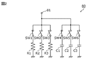
図2は、本実施の形態に係る方向性結合器1が備える終端回路80の一例を示す回路図である。図2に示されるように、終端回路80は、3つの抵抗R1〜R3と、3つのキャパシタC1〜C3と、6つのスイッチSW1〜SW6と、端子81とを含む。
FIG. 2 is a circuit diagram showing an example of a
端子81は、副線路20の他端22に接続される。本実施の形態では、端子81は、副線路20の他端22に方向切替回路70を介して接続されている。
The terminal 81 is connected to the
抵抗R1〜R3及びキャパシタC1〜C3はそれぞれ、6つのスイッチSW1〜SW6の1つと直列に接続されている。抵抗とスイッチとの直列回路、及び、キャパシタとスイッチとの直列回路が、端子81とグランドとの間に並列に接続されている。 The resistors R1 to R3 and the capacitors C1 to C3 are each connected in series with one of the six switches SW1 to SW6. A series circuit of the resistor and the switch and a series circuit of the capacitor and the switch are connected in parallel between the terminal 81 and the ground.
抵抗R1〜R3の各々の抵抗値は、互いに等しくてもよく、異なっていてもよい。キャパシタC1〜C3の各々の容量値は、互いに等しくてもよく、異なっていてもよい。また、3つの抵抗R1〜R3の1つにはスイッチが接続されていなくてもよい。3つのキャパシタC1〜C3の1つにはスイッチが接続されていなくてもよい。 The resistance values of the resistors R1 to R3 may be equal to or different from each other. The capacitance values of the capacitors C1 to C3 may be equal to or different from each other. Further, the switch may not be connected to one of the three resistors R1 to R3. A switch may not be connected to one of the three capacitors C1 to C3.
スイッチSW1〜SW6は、例えば、MOSFETなどのスイッチング素子である。スイッチSW1〜SW6は、オンオフ(導通/非導通)が切替可能である。これにより、終端回路80のインピーダンスを変更することができる。例えば、スイッチSW1〜SW6は、主線路10を伝送される高周波信号の基本周波数に基づいて調整される。具体的には、終端回路80のインピーダンスが、基本周波数の信号を終端回路80によって十分に吸収消費できるような値になるように、スイッチSW1〜SW6のオンオフが制御される。
The switches SW1 to SW6 are switching elements such as MOSFETs. The switches SW1 to SW6 can be switched on and off (conducting / non-conducting). Thereby, the impedance of the
なお、終端回路80は、1つ以上のインダクタを含んでもよい。また、終端回路80の回路構成は特に限定されない。終端回路80は、抵抗又はキャパシタを含んでいなくてもよい。
The
以上のように構成された方向性結合器1は、主線路10を伝送される高周波信号の検波に利用される。高周波信号は、例えば、Wi−Fi(登録商標)、LTE(Long Term Evolution)又は5G(5th Generation)などの通信規格に準拠した信号である。方向性結合器1は、例えば、マルチモード/マルチバンド対応の携帯電話のフロントエンド部に配置される。
The directional coupler 1 configured as described above is used for detecting a high frequency signal transmitted on the
主線路10を伝送される高周波信号の一部は、副線路20と、複数のフィルタ30及び31のいずれか又はバイパススイッチ55とを介して、結合出力端子40から出力される。結合出力端子40には、例えば、検波器(図示せず)が接続される。例えば、検波器は、入力される信号の信号電力などを検出し、検出結果を出力する。
A part of the high frequency signal transmitted on the
検出結果は、例えば、送信回路若しくは受信回路又はこれらの回路の制御回路に出力される。これにより、例えば、送信回路又は受信回路が備える増幅器の増幅率を検波結果に基づいて適切な値に変更するなどのように、送信又は受信に関わる処理を適切に制御することができる。検波精度を高めることで、各種制御の精度及び信頼性を高めることができる。 The detection result is output to, for example, a transmission circuit or a reception circuit, or a control circuit of these circuits. This makes it possible to appropriately control the processing related to transmission or reception, such as changing the amplification factor of the amplifier included in the transmission circuit or reception circuit to an appropriate value based on the detection result. By increasing the detection accuracy, the accuracy and reliability of various controls can be improved.
なお、方向性結合器1は、方向切替回路70及びバイパススイッチ55の少なくとも一方を備えていなくてもよい。また、終端回路80は、可変終端回路でなくてもよく、インピーダンスが固定の終端回路であってもよい。
The directional coupler 1 does not have to include at least one of the
また、ノードN1とノードN2との間に設けられるフィルタの個数は、3つ以上であってもよい。フィルタの個数に応じて、フィルタ切替回路及びフィルタ保護スイッチが設けられていればよい。 Further, the number of filters provided between the node N1 and the node N2 may be three or more. A filter changeover circuit and a filter protection switch may be provided according to the number of filters.
[1−2.動作(各スイッチのオンオフ状態)]
次に、本実施の形態に係る方向性結合器1の動作について説明する。以下では、主に各スイッチのオンオフ状態について説明する。各スイッチのオンオフ状態の切り替えは、図示されない制御回路によって制御される。
[1-2. Operation (on / off state of each switch)]
Next, the operation of the directional coupler 1 according to the present embodiment will be described. In the following, the on / off state of each switch will be mainly described. The switching of the on / off state of each switch is controlled by a control circuit (not shown).
方向性結合器1では、主線路10を伝送される高周波信号の一部が、主線路10と副線路20との電磁気的な結合によって、結合信号として副線路20に流れる。結合信号は、副線路20の一端21又は他端22から方向切替回路70を介して、ノードN1まで流れる。ノードN1に到達した結合信号は、複数のフィルタ30及び31から選択された1つのフィルタ又はバイパススイッチ55とノードN2とを通過し、結合出力端子40から出力される。
In the directional coupler 1, a part of the high frequency signal transmitted on the
このように、結合信号をノードN1からノードN2に流すために、フィルタ切替回路50及び51並びにバイパススイッチ55は、ノードN1とノードN2とを結ぶ経路が1つ以下になるように制御される。つまり、フィルタ切替回路50及び51並びにバイパススイッチ55は、ノードN1とノードN2との間に設けられた複数のフィルタ30及び31のうちの1つのみが選択されるように、又は、いずれも選択されないように制御される。
In this way, in order to send the coupling signal from the node N1 to the node N2, the
以下では、フィルタ切替回路50及び51によってノードN1とノードN2とに接続されたフィルタを「対象フィルタ」と記載する。対象フィルタ以外のフィルタを「非対象フィルタ」と記載する。対象フィルタは、結合信号が流れるフィルタである。
In the following, the filter connected to the node N1 and the node N2 by the
例えば、図1に示される例では、フィルタ切替回路50がオン状態であり、フィルタ30が対象フィルタになる。フィルタ31が非対象フィルタになるので、フィルタ切替回路51及びバイパススイッチ55はいずれもオフ状態である。
For example, in the example shown in FIG. 1, the
なお、バイパススイッチ55がオン状態である場合には、フィルタ切替回路50及び51はいずれもオフ状態になる。この場合、フィルタ30及び31のいずれも、非対象フィルタになる。なお、フィルタ切替回路50及び51並びにバイパススイッチ55の全てがオフ状態になってもよい。
When the
本実施の形態では、フィルタ切替回路50及び51のオンオフ状態と連動するように、複数のフィルタ保護スイッチ60a、60b、61a及び61bが制御される。具体的には、複数のフィルタ保護スイッチ60a、60b、61a及び61bは、対象フィルタの一端と基準電位との接続を開放し、かつ、非対象フィルタの一端と基準電位とを接続する。
In the present embodiment, a plurality of
図1に示される例では、対象フィルタであるフィルタ30の両端にそれぞれ接続されたフィルタ保護スイッチ60a及び60bは、オフ状態である。つまり、フィルタ保護スイッチ60a及び60bは、フィルタ30の両端とグランドとの接続を開放している。これにより、主線路10から副線路20に電磁気的に結合された結合信号を、ノードN1からフィルタ30を介してノードN2に通過させることができる。
In the example shown in FIG. 1, the
一方で、非対象フィルタであるフィルタ31の両端にそれぞれ接続されたフィルタ保護スイッチ61a及び61bは、オン状態である。つまり、フィルタ保護スイッチ61a及び61bは、フィルタ31の両端とグランドとを接続している。
On the other hand, the
このように、結合信号を流さない非対象フィルタであるフィルタ31の両端の電位を固定することで、フィルタ31の両端に大きな電位差が生じるのを抑制することができる。これにより、フィルタ31の静電気破壊を抑制することができる。
In this way, by fixing the potentials at both ends of the
なお、非対象フィルタの一端の電位のみを固定してもよい。例えば、フィルタ保護スイッチ61aのみがオン状態になり、フィルタ31のノードN1側の端部がグランドに接続されてもよい。あるいは、フィルタ保護スイッチ61bのみがオン状態になり、フィルタ31のノードN2側の端部がグランドに接続されてもよい。フィルタ31の両端の電位が不安定な場合に比べて、静電気破壊される可能性を低くすることができる。
It should be noted that only the potential at one end of the asymmetric filter may be fixed. For example, only the
このように、非対象フィルタの一端の電位のみを固定する場合には、フィルタの一端のみにフィルタ保護スイッチが設けられていればよい。したがって、フィルタ保護スイッチ60a及び60bの一方、並びに、フィルタ保護スイッチ61a及び61bの一方は設けられていなくてもよい。
In this way, when fixing only the potential at one end of the asymmetric filter, it is sufficient that the filter protection switch is provided only at one end of the filter. Therefore, one of the
[1−3.効果など]
以上のように、本実施の形態に係る方向性結合器1は、主線路10と、主線路10と電磁気的に結合する副線路20と、結合出力端子40と、複数のフィルタ30及び31と、複数のフィルタ30及び31の各々を、副線路20の一端21と結合出力端子40とに接続可能であるフィルタ切替回路50及び51と、複数のフィルタ30及び31の各々の一端に直接接続され、対応するフィルタの一端と基準電位との接続及び開放を切替可能である複数のフィルタ保護スイッチ60a、60b、61a及び61bと、を備える。
[1-3. Effect etc.]
As described above, the directional coupler 1 according to the present embodiment includes the
例えば、複数のフィルタ保護スイッチ60a、60b、61a及び61bは、複数のフィルタ30及び31の1つである対象フィルタをフィルタ切替回路50及び51が副線路20の一端21と結合出力端子40とに接続する場合に、対象フィルタの一端と基準電位との接続を開放し、かつ、対象フィルタ以外のフィルタの一端と基準電位とを接続する。
For example, the plurality of
これにより、非対象フィルタの一端の電位を基準電位に固定することができる。非対象フィルタの一端の電位が固定されることで、非対象フィルタが静電気破壊されるのを抑制することができ、フィルタの周波数特性の劣化を抑制することができる。 As a result, the potential at one end of the asymmetric filter can be fixed to the reference potential. By fixing the potential at one end of the asymmetric filter, it is possible to suppress electrostatic breakdown of the asymmetric filter, and it is possible to suppress deterioration of the frequency characteristics of the filter.
また、非対象フィルタの一端の電位が固定されるので、非対象フィルタが対象フィルタの通過特性に望ましくない影響を与える度合いを低減することができる。このため、結合出力端子40から取り出される信号の精度を高めることができる。
Further, since the potential at one end of the non-target filter is fixed, it is possible to reduce the degree to which the non-target filter adversely affects the passing characteristics of the target filter. Therefore, the accuracy of the signal extracted from the combined
また、例えば、複数のフィルタ30の両端にそれぞれ、フィルタ保護スイッチ60a、60b、61a及び61bが接続されている。
Further, for example,
これにより、非対象フィルタの両端の電位が固定されるので、非対象フィルタの保護性能を高めることができる。つまり、非対象フィルタが静電気破壊される可能性を十分に低くすることができるので、フィルタの周波数特性の劣化を更に抑制することができる。 As a result, the potentials at both ends of the asymmetric filter are fixed, so that the protection performance of the asymmetric filter can be improved. That is, since the possibility that the non-target filter is electrostatically destroyed can be sufficiently reduced, deterioration of the frequency characteristics of the filter can be further suppressed.
また、非対象フィルタが対象フィルタの通過特性に望ましくない影響を与える度合いを更に低減することができる。このため、結合出力端子40から取り出される信号の精度を更に高めることができる。
In addition, the degree to which the non-target filter adversely affects the passing characteristics of the target filter can be further reduced. Therefore, the accuracy of the signal extracted from the combined
また、例えば、副線路20の一端21と結合出力端子40とを結ぶ経路には、複数のフィルタ30及び31のいずれかを通過する複数の経路と、当該複数の経路への分岐点とが含まれる。複数のフィルタ30及び31の各々は、分岐点から見たときのインピーダンスが正のリアクタンスを持つ。
Further, for example, the path connecting one
これにより、開放されたフィルタ保護スイッチが持つオフ容量の負のリアクタンス成分を補償することができるので、フィルタの周波数特性が不要の劣化を起こすことを抑制することができる。この際、開放されたフィルタ保護スイッチのオフ容量が一定の損失分を持つが、当該損失分は、方向性結合器1の結合比に算入されるので問題にはならない。 As a result, it is possible to compensate for the negative reactance component of the off capacitance of the open filter protection switch, so that it is possible to suppress unnecessary deterioration of the frequency characteristics of the filter. At this time, the off capacitance of the opened filter protection switch has a certain loss amount, but this loss amount is included in the coupling ratio of the directional coupler 1, so that it does not matter.
また、例えば、本実施の形態に係る方向性結合器1は、さらに、副線路20の他端22に接続された終端回路80を備える。終端回路80は、可変終端回路である。
Further, for example, the directional coupler 1 according to the present embodiment further includes a
これにより、副線路20の他端22側で高周波信号を適切に終端回路80によって吸収消費することができる。例えば、進行波を結合出力端子40から取り出したい場合に、反射波を終端回路80によって吸収消費することができるので、取り出される信号の精度を高めることができる。
As a result, the high frequency signal can be appropriately absorbed and consumed by the
[1−4.変形例]
ここで、実施の形態1の変形例について、図3を用いて説明する。
[1-4. Modification example]
Here, a modified example of the first embodiment will be described with reference to FIG.
図3は、本変形例に係る方向性結合器1の別の動作状態を示す図である。なお、本変形例に係る方向性結合器の構成は実施の形態1と同じであるので、実施の形態1に係る方向性結合器1の構成を用いて本変形例の動作について説明する。 FIG. 3 is a diagram showing another operating state of the directional coupler 1 according to the present modification. Since the configuration of the directional coupler according to the present modification is the same as that of the first embodiment, the operation of the present modification will be described using the configuration of the directional coupler 1 according to the first embodiment.
上記実施の形態1では、非対象フィルタに接続されたフィルタ保護スイッチをオン状態にすることにより、非対象フィルタの一端又は両端を基準電位に接続する例を示した。これに対して、本変形例では、図3に示されるように、非対象フィルタであるフィルタ31に接続されたフィルタ保護スイッチ61a及び61bは、オフ状態である。つまり、非対象フィルタであるフィルタ31の一端又は両端は、基準電位に固定されない。
In the first embodiment, an example is shown in which one end or both ends of the asymmetric filter are connected to the reference potential by turning on the filter protection switch connected to the asymmetric filter. On the other hand, in this modification, as shown in FIG. 3, the
本変形例では、フィルタ保護スイッチ60a、60b、61a及び61bは、フィルタ切替回路50のオンオフ状態によらずに、常にオフ状態で維持される。具体的には、フィルタ保護スイッチ60a、60b、61a及び61bはそれぞれ、ツェナーダイオードとして機能させる。例えば、フィルタ保護スイッチ61aに大きな電圧がかかった場合には、フィルタ保護スイッチ61aがオン状態(ブレークダウン)になり、フィルタ保護スイッチ61aの両端間の電圧を一定に保つ。これにより、フィルタ保護スイッチ61aに接続されたフィルタ31の一端の電位を一定に保つことができる。フィルタ保護スイッチ61aが保持する電圧より大きい電圧がフィルタ31にかかることを抑制することができるので、フィルタ31を保護することができる。
In this modification, the
このように、本変形例に係る方向性結合器1では、複数のフィルタ保護スイッチ60a、60b、61a及び61bは、複数のフィルタ30及び31の各々の一端と基準電位との接続を開放する。
As described above, in the directional coupler 1 according to the present modification, the plurality of
これにより、実施の形態1の場合と同様に、フィルタの周波数特性の劣化を抑制することができる。 As a result, deterioration of the frequency characteristics of the filter can be suppressed as in the case of the first embodiment.
(実施の形態2)
続いて、実施の形態2について説明する。
(Embodiment 2)
Subsequently, the second embodiment will be described.
実施の形態2に係る方向性結合器では、フィルタ切替回路とフィルタ保護スイッチとの構成が実施の形態1とは主として異なる。以下では、実施の形態1との相違点を中心に説明を行い、共通点の説明を省略又は簡略化する。 In the directional coupler according to the second embodiment, the configuration of the filter changeover circuit and the filter protection switch is mainly different from that of the first embodiment. In the following, the differences from the first embodiment will be mainly described, and the common points will be omitted or simplified.
[2−1.構成]
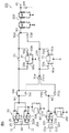
まず、実施の形態2に係る方向性結合器の構成について、図4を用いて説明する。図4は、本実施の形態に係る方向性結合器101の構成を示す図である。
[2-1. composition]
First, the configuration of the directional coupler according to the second embodiment will be described with reference to FIG. FIG. 4 is a diagram showing a configuration of a
図4に示されるように、方向性結合器101では、実施の形態1に係る方向性結合器1と比較して、フィルタ30及び31の各々とノードN1及びN2の各々との間に設けられたスイッチが、2つのシリーズスイッチと1つのシャントスイッチとを含むT型のスイッチ回路に置き換えられた点が異なっている。具体的には、方向性結合器101は、複数のフィルタ切替回路50及び51、複数のフィルタ保護スイッチ60a、60b、61a及び61b並びにバイパススイッチ55の代わりに、複数のフィルタ切替回路150及び151、複数のフィルタ保護回路160a、160b、161a及び161b並びにバイパススイッチ回路155を備える。本実施の形態においても、実施の形態1と同様に、例えば、複数のフィルタ30及び31以外の各素子は、方向性結合器101が備える半導体ICに形成されている。具体的には、複数のフィルタ切替回路150及び151、複数のフィルタ保護回路160a、160b、161a及び161b並びにバイパススイッチ回路155は、半導体ICに形成されている。
As shown in FIG. 4, the
複数のフィルタ切替回路150及び151は、複数のフィルタ30及び31の各々を、副線路20の一端21と結合出力端子40とに接続可能である第1スイッチ回路を構成している。フィルタ切替回路150は、フィルタ30に対応しており、フィルタ30とノードN1及びN2との接続及び開放を切り替える。フィルタ切替回路151は、フィルタ31に対応しており、フィルタ31とノードN1及びN2との接続及び開放を切り替える。
The plurality of
フィルタ切替回路150は、スイッチ150A、150B、150C及び150Dを含む。なお、フィルタ切替回路150は、スイッチ150A及び150Cのみを含んでもよく、スイッチ150B及び150Dのみを含んでもよい。
The
スイッチ150A及び150Bはそれぞれ、フィルタ30の一端に接続された第1スイッチの一例である。スイッチ150Aは、フィルタ30のノードN1側の端部に直接接続されている。スイッチ150Bは、フィルタ30のノードN2側の端部に直接接続されている。スイッチ150A及び150Bは、互いのオンオフ状態が同じになるように制御される。
The
スイッチ150C及び150Dはそれぞれ、第1スイッチと副線路20の一端21又は結合出力端子40との間に直列に接続された第2スイッチの一例である。スイッチ150Cは、スイッチ150AとノードN1との間に接続されている。スイッチ150Dは、スイッチ150BとノードN2との間に接続されている。スイッチ150C及び150Dは、互いのオンオフ状態が同じになるように制御される。
The
フィルタ切替回路151は、スイッチ151A、151B、151C及び151Dを含む。なお、フィルタ切替回路151は、スイッチ151A及び151Cのみを含んでもよく、スイッチ151B及び151Dのみを含んでもよい。
The
スイッチ151A及び151Bはそれぞれ、フィルタ31の一端に接続された第1スイッチの一例である。スイッチ151Aは、フィルタ31のノードN1側の端部に直接接続されている。スイッチ151Bは、フィルタ31のノードN2側の端部に直接接続されている。スイッチ151A及び151Bは、互いのオンオフ状態が同じになるように制御される。
The
スイッチ151C及び151Dはそれぞれ、第1スイッチと副線路20の一端21又は結合出力端子40との間に直列に接続された第2スイッチの一例である。スイッチ151Cは、スイッチ151AとノードN1との間に接続されている。スイッチ151Dは、スイッチ151BとノードN2との間に接続されている。スイッチ151C及び151Dは、互いのオンオフ状態が同じになるように制御される。
The
複数のフィルタ保護回路160a、160b、161a及び161bはそれぞれ、第2スイッチ回路の一例であり、複数のフィルタ30及び31の各々の一端と基準電位とに接続されている。複数のフィルタ保護回路160a、160b、161a及び161bはそれぞれ、対応するフィルタの一端と基準電位との接続及び開放を切替可能である。
The plurality of
フィルタ保護回路160aは、スイッチ150A及び160Aを含む。スイッチ150Aは、フィルタ保護回路160aとフィルタ切替回路150とで共用されている。スイッチ160Aは、スイッチ150A及び150Cの接続部分と基準電位との接続及び開放を切替可能な第3スイッチの一例である。具体的には、スイッチ160Aは、スイッチ150A及び150Cの接続部分とグランドとの各々に直接接続されている。フィルタ保護回路160aは、フィルタ30のノードN1側の端部とグランドとの接続及び開放を切り替える。
The
フィルタ保護回路160bは、スイッチ150B及び160Bを含む。スイッチ150Bは、フィルタ保護回路160bとフィルタ切替回路150とで共用されている。スイッチ160Bは、スイッチ150B及び150Dの接続部分と基準電位との接続及び開放を切替可能な第3スイッチの一例である。具体的には、スイッチ160Bは、スイッチ150B及び150Dの接続部分とグランドとの各々に直接接続されている。フィルタ保護回路160bは、フィルタ30のノードN2側の端部とグランドとの接続及び開放を切り替える。
The
フィルタ保護回路161aは、スイッチ151A及び161Aを含む。スイッチ151Aは、フィルタ保護回路161aとフィルタ切替回路151とで共用されている。スイッチ161Aは、スイッチ151A及び151Cの接続部分と基準電位との接続及び開放を切替可能な第3スイッチの一例である。具体的には、スイッチ161Aは、スイッチ151A及び151Cの接続部分とグランドとの各々に直接接続されている。フィルタ保護回路161aは、フィルタ31のノードN1側の端部とグランドとの接続及び開放を切り替える。
The
フィルタ保護回路161bは、スイッチ151B及び161Bを含む。スイッチ151Bは、フィルタ保護回路161bとフィルタ切替回路151とで共用されている。スイッチ161Bは、スイッチ151B及び151Dの接続部分と基準電位との接続及び開放を切替可能な第3スイッチの一例である。具体的には、スイッチ161Bは、スイッチ151B及び151Dの接続部分とグランドとの各々に直接接続されている。フィルタ保護回路161bは、フィルタ31のノードN2側の端部とグランドとの接続及び開放を切り替える。
The
バイパススイッチ回路155は、ノードN1とノードN2との間のバイパス経路の接続及び開放を切り替える。バイパススイッチ回路155は、スイッチ155a、155b及び155cを含む。スイッチ155a及び155bは、ノードN1とノードN2との間に互いに直列に接続されている。スイッチ155cは、スイッチ155aとスイッチ155bとの接続部分とグランドとの各々に直接接続されている。つまり、バイパススイッチ回路155は、T型のスイッチ回路である。
The
[2−2.動作(各スイッチのオンオフ状態)]
次に、本実施の形態に係る方向性結合器101の動作について説明する。以下では、主に各スイッチのオンオフ状態について説明する。各スイッチのオンオフ状態の切替は、図示されない制御回路によって制御される。
[2-2. Operation (on / off state of each switch)]
Next, the operation of the
方向性結合器101では、実施の形態1と同様に、結合信号をノードN1からノードN2に流すために、フィルタ切替回路150及び151並びにバイパススイッチ回路155は、ノードN1とノードN2とを結ぶ経路が1つ以下になるように制御される。図4では、フィルタ30がノードN1とノードN2とに接続された対象フィルタであり、フィルタ31が非対象フィルタである場合を説明する。
In the
図4に示されるように、フィルタ30をノードN1とノードN2とに接続するため、フィルタ切替回路150がオン状態になる。具体的には、スイッチ150A、150B、150C及び150Dの全てがオン状態になる。非対象フィルタであるフィルタ31に接続されたフィルタ切替回路151と、バイパススイッチ回路155とはいずれもオフ状態である。
As shown in FIG. 4, since the
本実施の形態では、フィルタ切替回路150及び151のオンオフ状態と連動するように、複数のフィルタ保護回路160a、160b、161a及び161bが制御される。具体的には、複数のフィルタ保護回路160a、160b、161a及び161bは、対象フィルタの一端と基準電位との接続を開放し、かつ、非対象フィルタの一端と基準電位とを接続する。
In the present embodiment, a plurality of
図4に示されるように、対象フィルタであるフィルタ30の両端にそれぞれ接続されたフィルタ保護回路160a及び160bは、オフ状態である。具体的には、T型のスイッチ回路のシャントスイッチに相当するスイッチ160A及び160Bのみが、オフ状態である。フィルタ保護回路160a及び160bのうち、フィルタ切替回路150と共用されるスイッチ150A及び150Bは、オン状態である。これにより、フィルタ保護回路160a及び160bは、フィルタ30の両端とグランドとの接続を開放している。したがって、主線路10から副線路20に電磁気的に結合された結合信号を、ノードN1からフィルタ30を介してノードN2に通過させることができる。
As shown in FIG. 4, the
一方で、非対象フィルタであるフィルタ31の両端にそれぞれ接続されたフィルタ保護回路161a及び161bは、オン状態である。具体的には、スイッチ151A、161A、151B及び161Bのいずれもが、オン状態である。これにより、フィルタ保護回路161a及び161bは、フィルタ31の両端とグランドとを接続している。
On the other hand, the
なお、フィルタ31をノードN1及びN2から切り離すため、フィルタ切替回路151に含まれるスイッチ151C及び151Dをオフ状態にする。これにより、フィルタ保護回路160a及び160bに含まれるスイッチ151A及び151Bがオン状態であっても、フィルタ31とノードN1及びN2の各々とを開放することができる。本実施の形態では、スイッチ150A、150B、151A及び151Bは、接続されたフィルタが対象フィルタか非対象フィルタかによらずに、常にオン状態で維持される。
In order to separate the
このように、結合信号を流さない非対象フィルタであるフィルタ31の両端の電位を固定することで、フィルタ31の両端に大きな電位差が生じるのを抑制することができる。これにより、フィルタ31の静電気破壊を抑制することができる。
In this way, by fixing the potentials at both ends of the
なお、本実施の形態においても、実施の形態1と同様に、非対象フィルタの一端の電位のみを固定してもよい。この場合、フィルタ保護回路160a及び160bの一方、並びに、フィルタ保護回路161a及び161bの一方は設けられていなくてもよい。
In the present embodiment as well, as in the first embodiment, only the potential at one end of the non-target filter may be fixed. In this case, one of the
[2−3.効果など]
以上のように、本実施の形態に係る方向性結合器101は、主線路10と、主線路10と電磁気的に結合する副線路20と、結合出力端子40と、複数のフィルタ30及び31と、複数のフィルタ30及び31の各々を、副線路20の一端21と結合出力端子40とに接続可能であるフィルタ切替回路150及び151と、複数のフィルタ30及び31の各々の一端に接続され、対応するフィルタの一端と基準電位との接続及び開放を切替可能である複数のフィルタ保護回路160a、160b、161a及び161bと、を備える。複数のフィルタ保護回路160a、160b、161a及び161bは、複数のフィルタ30及び31の1つである対象フィルタをフィルタ切替回路150及び151が副線路20の一端21と結合出力端子40とに接続する場合に、対象フィルタの一端と基準電位との接続を開放し、かつ、対象フィルタ以外のフィルタの一端と基準電位とを接続する。
[2-3. Effect etc.]
As described above, the
これにより、実施の形態1の場合と同様に、非対象フィルタの一端の電位が固定されることで、非対象フィルタが静電気破壊されるのを抑制することができ、フィルタの周波数特性の劣化を抑制することができる。また、非対象フィルタが対象フィルタの通過特性に望ましくない影響を与える度合いを低減することができるので、結合出力端子40から取り出される信号の精度を高めることができる。
As a result, as in the case of the first embodiment, the potential at one end of the asymmetric filter is fixed, so that the asymmetric filter can be suppressed from being electrostatically destroyed, and the frequency characteristics of the filter are deteriorated. It can be suppressed. Further, since the degree to which the non-target filter adversely affects the passing characteristics of the target filter can be reduced, the accuracy of the signal extracted from the coupled
また、例えば、フィルタ切替回路150及び151は、複数のフィルタ30及び31の各々の一端に接続された第1スイッチと、第1スイッチと副線路20の一端21又は結合出力端子40との間に直列に接続された第2スイッチと、を含む。複数のフィルタ保護回路160a、160b、161a及び161bはそれぞれ、第1スイッチと、第1スイッチ及び第2スイッチの接続部分と基準電位との接続及び開放を切替可能な第3スイッチと、を含む。対象フィルタをフィルタ切替回路150及び151が副線路20の一端21と結合出力端子40とに接続する場合に、対象フィルタ以外のフィルタの一端に接続されたフィルタ保護回路160a、160b、161a又は161bの第1スイッチ及び第3スイッチは、対象フィルタ以外のフィルタの一端と基準電位とを接続する。
Further, for example, the
これにより、フィルタの切替と非対象フィルタの保護とを両立させることができる。 As a result, it is possible to achieve both filter switching and protection of the asymmetric filter.
また、例えば、複数のフィルタ30及び31の両端にそれぞれ、フィルタ保護回路160a、160b、161a及び161bが接続されている。
Further, for example,
これにより、非対象フィルタが静電気破壊される可能性を十分に低くすることができるので、フィルタの周波数特性の劣化を更に抑制することができる。また、非対象フィルタが対象フィルタの通過特性に望ましくない影響を与える度合いを更に低減することができるので、結合出力端子40から取り出される信号の精度を更に高めることができる。
As a result, the possibility that the non-target filter is electrostatically destroyed can be sufficiently reduced, so that deterioration of the frequency characteristics of the filter can be further suppressed. Further, since the degree to which the non-target filter adversely affects the passing characteristics of the target filter can be further reduced, the accuracy of the signal extracted from the coupled
(実施の形態3)
続いて、実施の形態3について説明する。
(Embodiment 3)
Subsequently, the third embodiment will be described.
実施の形態3では、主線路及び副線路がそれぞれ複数である点が実施の形態1及び2と主として異なる。以下では、実施の形態1及び2との相違点を中心に説明を行い、共通点の説明を省略又は簡略化する。 The third embodiment is mainly different from the first and second embodiments in that the number of main lines and the number of sub lines are each. In the following, the differences from the first and second embodiments will be mainly described, and the common points will be omitted or simplified.
[3−1.構成]
まず、実施の形態3に係る方向性結合器201の構成について、図5を用いて説明する。図5は、本実施の形態に係る方向性結合器201の構成を示す図である。
[3-1. composition]
First, the configuration of the
図5に示されるように、方向性結合器201は、2つの主線路10及び210と、3つの副線路20、20A及び220と、2つのフィルタ30及び31と、結合出力端子40とを備える。さらに、方向性結合器201は、複数のスイッチ50a〜50d、51a〜51e、250c、251c及び251eと、フィルタ保護スイッチ60a、60b、61a及び61bと、バイパススイッチ55及び255と、方向切替回路70、70A及び270と、終端回路80及び280とを備える。さらに、方向性結合器201は、可変アッテネータ290と、端子保護スイッチ295とを備える。
As shown in FIG. 5, the
本実施の形態では、主線路10は、2つの副線路20及び20Aと電磁気的に結合している。このため、主線路10を伝送される高周波信号の一部は、副線路20及び20Aの各々に、結合信号として流れる。
In this embodiment, the
副線路20Aは、一端21A及び他端22Aを有する。一端21A及び他端22Aは、方向切替回路70Aを介して、結合出力端子40及び終端回路80のいずれかに選択的に接続される。副線路20Aは、例えば、線路の長さが副線路20とは異なっている。
The
主線路210は、2つの入出力端子211及び212を有する。入出力端子211は、送信回路及び受信回路の少なくとも一方に接続される。入出力端子212は、アンテナに接続される。なお、入出力端子212がアンテナに接続され、入出力端子211が送信回路又は受信回路に接続されてもよい。
The
主線路10が接続される送信回路又は受信回路と、主線路210が接続される送信回路又は受信回路は同じであってもよく、異なっていてもよい。同様に、主線路10が接続されるアンテナと主線路210が接続されるアンテナとは同じであってもよく、異なっていてもよい。
The transmission circuit or reception circuit to which the
主線路210は、副線路220と電磁気的に結合している。主線路210を伝送される高周波信号の一部は、副線路220に結合信号として流れる。
The
副線路220は、一端221及び他端222を有する。一端221及び他端222は、方向切替回路270を介して、結合出力端子40及び終端回路280のいずれかに選択的に接続される。
The
方向切替回路70A及び270は、実施の形態1に係る方向切替回路70と同じ構成を有する。方向切替回路70、70A及び270は、3つの副線路20、20A及び220のうちの1つの副線路の一端を結合出力端子40に接続し、かつ、他端を終端回路80又は280に接続するように構成されている。例えば、図5に示される例では、方向切替回路70によって、副線路20の一端21が結合出力端子40に接続され、他端22が終端回路80に接続されている。このとき、方向切替回路70A及び270はそれぞれ、副線路20A及び220の各々の両端を開放している。これにより、副線路20A又は220を流れる結合信号が結合出力端子40に混入するのを抑制することができる。なお、方向切替回路70、70A及び270の少なくとも1つは設けられていなくてもよい。3つの副線路20、20A及び220から1つの副線路を選択し、選択した副線路の一端を結合出力端子40に接続するスイッチが設けられていてもよい。
The
複数のスイッチ50a〜50d、51a〜51e、250c、251c及び251eと、バイパススイッチ55及び255とは、ノードN1とノードN2との間の複数の経路、及び、ノードN3とノードN2との間の複数の経路のうちの1つの経路を選択して接続するように構成されている。なお、ノードN1は、主線路10に対応しており、副線路20の一端21及び他端22、並びに、副線路20Aの一端21A及び他端22Aのうちの1つが方向切替回路70又は70Aによって接続される。ノードN3は、主線路210に対応しており、副線路220の一端221及び他端222の一方が方向切替回路270によって接続される。
The plurality of
スイッチ50cは、ノードN1とスイッチ50aとに接続されている。スイッチ50dは、スイッチ50bとノードN2とに接続されている。
The
スイッチ50cとスイッチ50dとの間には、バイパススイッチ55が接続されている。バイパススイッチ55の両端に、スイッチ50a、フィルタ30及びスイッチ50bの直列回路が接続されている。つまり、バイパススイッチ55は、フィルタ30を通過しない経路の接続及び開放を切替可能なスイッチである。
A
スイッチ51cは、ノードN1とスイッチ51aとの間にスイッチ51eを介して接続されている。スイッチ51dは、スイッチ51bとノードN2とに接続されている。スイッチ51eは、スイッチ51cとスイッチ51aとに接続されている。
The
スイッチ51eとスイッチ51dとの間には、バイパススイッチ255が接続されている。バイパススイッチ255の両端に、スイッチ51a、フィルタ31及びスイッチ51bの直列回路が接続されている。つまり、バイパススイッチ255は、フィルタ31を通過しない経路の接続及び開放を切替可能なスイッチである。なお、バイパススイッチ55及び255の少なくとも一方は、設けられていなくてもよい。
A
スイッチ250cは、ノードN3とスイッチ50aとに接続されている。スイッチ251cは、ノードN3とスイッチ51aとの間にスイッチ251eを介して接続されている。スイッチ251eは、スイッチ251cとスイッチ51aとに接続されている。
The
可変アッテネータ290は、結合出力端子40と副線路20、20A又は220の一端とを結ぶ経路上に配置されている。具体的には、可変アッテネータ290は、ノードN2と結合出力端子40とに接続されている。
The
可変アッテネータ290は、結合出力端子40から出力される信号の出力を変更する回路である。図5に示される例では、可変アッテネータ290は、6つの抵抗と6つのスイッチとを含んでいるが、回路構成例は特に限定されない。例えば、スイッチ51e及び251eなどは設けられていなくてもよい。
The
端子保護スイッチ295は、結合出力端子40と基準電位との接続及び開放を切替可能なスイッチである。具体的には、端子保護スイッチ295は、結合出力端子40とグランドとに直接接続されている。
The
端子保護スイッチ295は、常にオフ状態で維持される。つまり、端子保護スイッチ295は、結合出力端子40とグランドとの間を開放している。具体的には、端子保護スイッチ295は、ツェナーダイオードとして機能させる。例えば、結合出力端子40に大きな電圧がかかった場合には、端子保護スイッチ295がオン状態になり、端子保護スイッチ295の両端間の電圧を一定に保つ。これにより、端子保護スイッチ295に接続された結合出力端子40の電位を一定に保つことができる。端子保護スイッチ295が保持する電圧より大きい電圧が結合出力端子40にかかることを抑制することができるので、結合出力端子40を保護することができる。
The
図5に示される各スイッチの個数、配置及び接続関係は、一例に過ぎない。複数の副線路と複数のフィルタとの接続の組み合わせを変更可能に構成されていれば、スイッチの個数、配置及び接続関係は適宜変更可能である。 The number, arrangement, and connection relationship of each switch shown in FIG. 5 are only an example. If the combination of the connection between the plurality of sub-lines and the plurality of filters can be changed, the number, arrangement, and connection relationship of the switches can be changed as appropriate.
また、ノードN1又はN3と結合出力端子40との間には、整合回路が設けられていてもよい。整合回路は、1つ以上のキャパシタ及び1つ以上のインダクタを含む。
Further, a matching circuit may be provided between the node N1 or N3 and the
また、方向性結合器201は、3つ以上の主線路を備えてもよい。また、1つの主線路に3つ以上の副線路が電磁気的に結合されてもよい。
Further, the
[3−2.動作(各スイッチのオンオフ状態)]
次に、本実施の形態に係る方向性結合器201の動作について説明する。以下では、主に各スイッチのオンオフ状態について説明する。各スイッチのオンオフ状態の切り替えは、図示されない制御回路によって制御される。
[3-2. Operation (on / off state of each switch)]
Next, the operation of the
方向性結合器201では、主線路10を伝送される高周波信号の一部が、主線路10と副線路20又は20Aとの電磁気的な結合によって、結合信号として副線路20又は20Aに流れる。結合信号は、副線路20又は20Aの端部から方向切替回路70又は70Aを介して、ノードN1まで流れる。ノードN1に到達した結合信号は、複数のフィルタ30及び31から選択された1つのフィルタ又はバイパススイッチ55若しくは255とノードN2とを通過し、結合出力端子40から出力される。
In the
また、主線路210を伝送される高周波信号の一部が、主線路210と副線路220との電磁気的な結合によって、結合信号として副線路220に流れる。結合信号は、副線路220の端部から方向切替回路270を介して、ノードN3まで流れる。ノードN3に到達した結合信号は、複数のフィルタ30及び31から選択された1つのフィルタ又はバイパススイッチ55若しくは255とノードN2とを通過し、結合出力端子40から出力される。
Further, a part of the high frequency signal transmitted on the
本実施の形態では、スイッチ50c、51c及び51e、並びに、スイッチ250c、251c及び251eは、主線路の選択に利用される。具体的には、主線路10を選択する場合、すなわち、主線路10から副線路20又は20Aに結合された結合信号を結合出力端子40から取り出す場合には、スイッチ50cと、スイッチ51c及び51eの双方とのいずれかがオン状態になる。これにより、主線路10に基づく結合信号は、ノードN1から、フィルタ30及び31並びにバイパススイッチ55及び255のいずれかを通ってノードN2に到達し、可変アッテネータ290を介して結合出力端子40から出力される。
In this embodiment, the
主線路210を選択する場合、すなわち、主線路210から副線路220に結合された結合信号を結合出力端子40から取り出す場合には、スイッチ250cと、スイッチ251c及び251eの双方とのいずれかがオン状態になる。これにより、主線路210に基づく結合信号は、ノードN3から、フィルタ30及び31並びにバイパススイッチ55及び255のいずれかを通ってノードN2に到達し、可変アッテネータ290を介して結合出力端子40から出力される。
When the
本実施の形態では、ノードN1又はN3とノードN2との経路の接続に利用されるスイッチ以外のスイッチはオフ状態になる。例えば、図5に示される例では、フィルタ30が対象フィルタであり、ノードN1からフィルタ30を通りノードN2に至る経路が接続されている。このため、フィルタ30を通る経路上に配置されたスイッチ50c、50a、50b及び50dがオン状態である。当該経路以外に配置されたスイッチ51c〜51e、250c、251c及び251e、並びに、バイパススイッチ55及び255はいずれもオフ状態である。
In the present embodiment, the switches other than the switches used for connecting the route between the node N1 or N3 and the node N2 are turned off. For example, in the example shown in FIG. 5, the
また、本実施の形態において、フィルタ保護スイッチ60a、60b、61a及び61bは、実施の形態1と同様に、対象フィルタに接続されている場合にオフ状態になり、非対象フィルタに接続されている場合にオン状態になる。例えば、図5に示されるように、対象フィルタであるフィルタ30に接続されたフィルタ保護スイッチ60a及び60bはオフ状態である。また、非対象フィルタであるフィルタ31に接続されたフィルタ保護スイッチ61a及び61bはオン状態である。これにより、フィルタ31の両端の電位がグランドに固定されるので、フィルタ31の静電気破壊を抑制することができる。
Further, in the present embodiment, the
[3−3.効果など]
以上のように、本実施の形態に係る方向性結合器201は、結合出力端子40と副線路20の一端21とを結ぶ経路上に配置された可変アッテネータ290を備える。
[3-3. Effect etc.]
As described above, the
これにより、結合出力を調整することができる。このため、例えば、結合出力端子40に接続される検波器において精度良く検波可能な出力レベルの信号を、結合出力端子40から出力することができる。
This allows the combined output to be adjusted. Therefore, for example, a signal having an output level that can be detected accurately by the detector connected to the combined
また、例えば、方向性結合器201は、さらに、結合出力端子40と基準電位との接続及び開放を切替可能な端子保護スイッチ295を備える。
Further, for example, the
これにより、結合出力端子40から侵入する不要な高電圧からフィルタ30及び31、並びに、可変アッテネータ290などを保護することができる。
Thereby, the
また、例えば、方向性結合器201は、複数の副線路20、20A及び220を備える。方向性結合器201は、さらに、複数の副線路20、20A及び220の各々の一端と結合出力端子40とを結ぶ経路を切替可能なスイッチを備える。
Further, for example, the
これにより、複数の副線路が設けられていることで、より広い周波数範囲又はより多いスペクトラムの中から取り出したい信号を選択して取り出すことができる。 As a result, by providing a plurality of sub-lines, it is possible to select and extract a signal to be extracted from a wider frequency range or a larger spectrum.
また、例えば、方向性結合器201は、複数の主線路10及び210を備える。複数の副線路20、20A及び220はそれぞれ、複数の主線路10及び210のいずれか1つに電磁気的に結合する。
Further, for example, the
これにより、複数の主線路が設けられていることで、より広い周波数範囲又はより多いスペクトラムの中から取り出したい信号を選択して取り出すことができる。 As a result, since a plurality of main lines are provided, it is possible to select and extract a signal to be extracted from a wider frequency range or a larger spectrum.
(その他)
以上、本発明に係る方向性結合器について、上記の実施の形態に基づいて説明したが、本発明は、上記の実施の形態に限定されるものではない。
(others)
Although the directional coupler according to the present invention has been described above based on the above-described embodiment, the present invention is not limited to the above-described embodiment.
例えば、フィルタ30及び31の少なくとも一方は、チューニング可能であってもよい。つまり、フィルタ30及び31の少なくとも一方は、通過帯域などの周波数特性を変更可能であってもよい。チューニングには、例えばスイッチ又はバラクタが用いられるが、これに限定されない。
For example, at least one of the
その他、各実施の形態に対して当業者が思いつく各種変形を施して得られる形態や、本発明の趣旨を逸脱しない範囲で各実施の形態における構成要素及び機能を任意に組み合わせることで実現される形態も本発明に含まれる。 In addition, it can be realized by arbitrarily combining the components and functions in each embodiment within the range obtained by applying various modifications to each embodiment and the purpose of the present invention. Forms are also included in the present invention.
本発明は、方向性結合器を含む電子機器及び通信機器などに利用することができる。 The present invention can be used for electronic devices including directional couplers, communication devices, and the like.
1、101、201 方向性結合器
10、210 主線路
11、12、211、212 入出力端子
20、20A、220 副線路
21、21A、221 一端
22、22A、222 他端
30、31 フィルタ
40 結合出力端子
50、51、150、151 フィルタ切替回路
50a、50b、50c、50d、51a、51b、51c、51d、51e、150A、150B、150C、150D、151A、151B、151C、151D、155a、155b、155c、160A、160B、161A、161B、250c、251c、251e スイッチ
55、255 バイパススイッチ
60a、60b、61a、61b フィルタ保護スイッチ
70、70A、270 方向切替回路
71、72、73、74、81 端子
80、280 終端回路
155 バイパススイッチ回路
160a、160b、161a、161b フィルタ保護回路
290 可変アッテネータ
295 端子保護スイッチ
N1、N2、N3 ノード
1, 101, 201
Claims (13)
前記主線路と電磁気的に結合する副線路と、
出力端子と、
複数のフィルタと、
前記複数のフィルタの各々を、前記副線路の一端と前記出力端子とに接続可能であるスイッチ回路と、
前記複数のフィルタの各々の両端にそれぞれ直接接続され、対応するフィルタの一端と基準電位との接続及び開放を切替可能である複数のスイッチと、を備える、
方向性結合器。 Main line and
A sub line that is electromagnetically coupled to the main line,
With the output terminal
With multiple filters
A switch circuit capable of connecting each of the plurality of filters to one end of the sub line and the output terminal.
It comprises a plurality of switches that are directly connected to both ends of each of the plurality of filters and can switch between the connection and the opening of one end of the corresponding filter and the reference potential.
Directional coupler.
請求項1に記載の方向性結合器。 The plurality of switches connect one end of the target filter to the reference potential when the switch circuit connects the target filter, which is one of the plurality of filters, to one end of the sub line and the output terminal. And connect one end of a filter other than the target filter to the reference potential.
The directional coupler according to claim 1.
請求項1に記載の方向性結合器。 The plurality of switches open the connection between one end of each of the plurality of filters and the reference potential.
The directional coupler according to claim 1.
前記半導体ICと接続された1以上の外部素子と、をさらに備え、
前記主線路と、前記副線路と、前記スイッチ回路と、前記複数のスイッチとは、前記半導体ICに形成され、
前記複数のフィルタは、前記1以上の外部素子により形成されている、
請求項1〜3のいずれか1項に記載の方向性結合器。 Semiconductor IC and
Further comprising one or more external elements connected to the semiconductor IC.
The main line, the sub line, the switch circuit, and the plurality of switches are formed on the semiconductor IC.
The plurality of filters are formed by the one or more external elements.
The directional coupler according to any one of claims 1 to 3.
前記主線路と電磁気的に結合する副線路と、
出力端子と、
複数のフィルタと、
前記複数のフィルタの各々を、前記副線路の一端と前記出力端子とに接続可能である第1スイッチ回路と、
前記複数のフィルタの各々の両端にそれぞれ接続され、対応するフィルタの一端と基準電位との接続及び開放を切替可能である複数の第2スイッチ回路と、を備え、
前記複数の第2スイッチ回路は、前記複数のフィルタの1つである対象フィルタを前記第1スイッチ回路が前記副線路の一端と前記出力端子とに接続する場合に、前記対象フィルタの一端と前記基準電位との接続を開放し、かつ、前記対象フィルタ以外のフィルタの一端と前記基準電位とを接続する、
方向性結合器。 Main line and
A sub line that is electromagnetically coupled to the main line,
With the output terminal
With multiple filters
A first switch circuit capable of connecting each of the plurality of filters to one end of the sub line and the output terminal, and
A plurality of second switch circuits, which are connected to both ends of each of the plurality of filters and can switch the connection and opening between one end of the corresponding filter and the reference potential, are provided.
The plurality of second switch circuits include one end of the target filter and the target filter when the first switch circuit connects one end of the sub line and the output terminal to the target filter which is one of the plurality of filters. The connection with the reference potential is opened, and one end of a filter other than the target filter is connected to the reference potential.
Directional coupler.
前記複数のフィルタの各々の一端に接続された第1スイッチと、
前記第1スイッチと前記副線路の一端又は前記出力端子との間に直列に接続された第2スイッチと、を含み、
前記複数の第2スイッチ回路はそれぞれ、
前記第1スイッチと、
前記第1スイッチ及び前記第2スイッチの接続部分と前記基準電位との接続及び開放を切替可能な第3スイッチと、を含み、
前記対象フィルタを前記第1スイッチ回路が前記副線路の一端と前記出力端子とに接続する場合に、前記対象フィルタ以外のフィルタの一端に接続された前記第2スイッチ回路の前記第1スイッチ及び前記第3スイッチは、前記対象フィルタ以外のフィルタの一端と前記基準電位とを接続する、
請求項5に記載の方向性結合器。 The first switch circuit is
A first switch connected to one end of each of the plurality of filters,
A second switch connected in series between the first switch and one end of the sub line or the output terminal is included.
Each of the plurality of second switch circuits
With the first switch
A third switch capable of switching connection and opening between the first switch and the connection portion of the second switch and the reference potential is included.
When the first switch circuit connects the target filter to one end of the sub line and the output terminal, the first switch and the first switch of the second switch circuit connected to one end of a filter other than the target filter. The third switch connects one end of a filter other than the target filter to the reference potential.
The directional coupler according to claim 5.
前記半導体ICと接続された1以上の外部素子と、をさらに備え、
前記主線路と、前記副線路と、前記第1スイッチ回路と、前記複数の第2スイッチ回路とは、前記半導体ICに形成され、
前記複数のフィルタは、前記1以上の外部素子により形成されている、
請求項5又は6に記載の方向性結合器。 Semiconductor IC and
Further comprising one or more external elements connected to the semiconductor IC.
The main line, the sub line, the first switch circuit, and the plurality of second switch circuits are formed in the semiconductor IC.
The plurality of filters are formed by the one or more external elements.
The directional coupler according to claim 5 or 6.
前記複数のフィルタの各々は、前記分岐点から見たときのインピーダンスが正のリアクタンスを持つ
請求項1〜7のいずれか1項に記載の方向性結合器。 The path connecting one end of the sub line and the output terminal includes a plurality of paths passing through any of the plurality of filters and a branch point to the plurality of paths.
The directional coupler according to any one of claims 1 to 7, wherein each of the plurality of filters has a positive reactance in impedance when viewed from the branch point.
請求項1〜8のいずれか1項に記載の方向性結合器。 Further, a variable termination circuit connected to the other end of the sub line is provided.
The directional coupler according to any one of claims 1 to 8.
請求項1〜9のいずれか1項に記載の方向性結合器。 Further, a variable attenuator arranged on a path connecting the output terminal and one end of the sub line is provided.
The directional coupler according to any one of claims 1 to 9.
請求項1〜9のいずれか1項に記載の方向性結合器。 Further, it is provided with a switch capable of switching connection and opening between the output terminal and the reference potential.
The directional coupler according to any one of claims 1 to 9.
さらに、複数の前記副線路の各々の一端と前記出力端子とを結ぶ経路を切替可能なスイッチを備える、
請求項1〜11のいずれか1項に記載の方向性結合器。 With multiple sub-tracks
Further, a switch capable of switching a path connecting one end of each of the plurality of sub-lines and the output terminal is provided.
The directional coupler according to any one of claims 1 to 11.
複数の前記副線路は、複数の前記主線路のいずれか1つに電磁気的に結合する、
請求項12に記載の方向性結合器。 Equipped with multiple main lines
The plurality of sub-lines are electromagnetically coupled to any one of the plurality of main lines.
The directional coupler according to claim 12.
Priority Applications (3)
| Application Number | Priority Date | Filing Date | Title |
|---|---|---|---|
| JP2020094470A JP2021190841A (en) | 2020-05-29 | 2020-05-29 | Directional coupler |
| CN202110554996.0A CN113746445A (en) | 2020-05-29 | 2021-05-20 | Directional coupler |
| US17/331,080 US20210376441A1 (en) | 2020-05-29 | 2021-05-26 | Directional coupler |
Applications Claiming Priority (1)
| Application Number | Priority Date | Filing Date | Title |
|---|---|---|---|
| JP2020094470A JP2021190841A (en) | 2020-05-29 | 2020-05-29 | Directional coupler |
Publications (1)
| Publication Number | Publication Date |
|---|---|
| JP2021190841A true JP2021190841A (en) | 2021-12-13 |
Family
ID=78705630
Family Applications (1)
| Application Number | Title | Priority Date | Filing Date |
|---|---|---|---|
| JP2020094470A Pending JP2021190841A (en) | 2020-05-29 | 2020-05-29 | Directional coupler |
Country Status (3)
| Country | Link |
|---|---|
| US (1) | US20210376441A1 (en) |
| JP (1) | JP2021190841A (en) |
| CN (1) | CN113746445A (en) |
Family Cites Families (10)
| Publication number | Priority date | Publication date | Assignee | Title |
|---|---|---|---|---|
| FR3004007A1 (en) * | 2013-03-29 | 2014-10-03 | St Microelectronics Tours Sas | BROADBAND COUPLER |
| US10276911B2 (en) * | 2015-03-27 | 2019-04-30 | Sony Semiconductor Solutions Corporation | Signal processing circuit, signal processing module, and communication apparatus |
| CN105024767B (en) * | 2015-06-16 | 2017-10-31 | 京信通信系统(广州)有限公司 | The standing wave detecting device and method of multiplefrequency mixer |
| CN204795056U (en) * | 2015-06-16 | 2015-11-18 | 京信通信系统(广州)有限公司 | Standing wave detection device of multiplefrequency mixer |
| CN108292793B (en) * | 2015-09-10 | 2021-03-09 | 天工方案公司 | Electromagnetic coupler for multi-frequency power detection |
| TW201713032A (en) * | 2015-09-17 | 2017-04-01 | 力智電子股份有限公司 | Preamplifier |
| WO2017136631A1 (en) * | 2016-02-05 | 2017-08-10 | Skyworks Solutions, Inc. | Electromagnetic couplers with multi-band filtering |
| CN107861429A (en) * | 2017-11-16 | 2018-03-30 | 成都爆米花信息技术有限公司 | A kind of data acquisition and switching system based on multisensor |
| WO2019189232A1 (en) * | 2018-03-28 | 2019-10-03 | 株式会社村田製作所 | Directional coupler |
| JP6881406B2 (en) * | 2018-08-31 | 2021-06-02 | 株式会社村田製作所 | Directional coupler |
-
2020
- 2020-05-29 JP JP2020094470A patent/JP2021190841A/en active Pending
-
2021
- 2021-05-20 CN CN202110554996.0A patent/CN113746445A/en active Pending
- 2021-05-26 US US17/331,080 patent/US20210376441A1/en active Pending
Also Published As
| Publication number | Publication date |
|---|---|
| US20210376441A1 (en) | 2021-12-02 |
| CN113746445A (en) | 2021-12-03 |
Similar Documents
| Publication | Publication Date | Title |
|---|---|---|
| KR102492079B1 (en) | RF switch with bypass topology | |
| US5778306A (en) | Low loss high frequency transmitting/receiving switching module | |
| JP2002290104A (en) | High-frequency switching circuit and communication terminal equipment using the same | |
| US11967977B2 (en) | Switch circuit, radio frequency front-end circuit, and communication device | |
| US9520628B2 (en) | Transistor switches with single-polarity control voltage | |
| US20100225378A1 (en) | Radio frequency switching circuit and semiconductor device | |
| JP2019068194A (en) | Front end module and communication apparatus | |
| KR101345975B1 (en) | Rf switches | |
| US10141927B2 (en) | Optimized RF switching device architecture for impedance control applications | |
| JP2010521830A (en) | RF switch and device comprising RF switch | |
| US11322817B2 (en) | Directional coupler and directional coupler module | |
| EP1440511B1 (en) | Compact 180 degree phase shifter | |
| JP2021190841A (en) | Directional coupler | |
| CN113054913B (en) | high frequency circuit | |
| US20220085794A1 (en) | Configurable micro-acoustic rf filter | |
| WO2022019178A1 (en) | Directional coupler | |
| US10200031B2 (en) | Electronically switchable diplexer | |
| JP2015119319A (en) | High frequency circuit | |
| WO2021241050A1 (en) | Directional coupler | |
| JP2012095257A (en) | Variable attenuator and variable attenuation device | |
| TWI790052B (en) | Radio frequency switch | |
| EP3160046B1 (en) | Matching network circuit, and associated apparatus with shared matching network circuit | |
| US6518822B1 (en) | High-frequency switch | |
| JP2008271408A (en) | Phase shift circuit | |
| KR20180037876A (en) | Antenna switch circuit with improved harmonic suppression characteristic |