WO2022019178A1 - Directional coupler - Google Patents
Directional coupler Download PDFInfo
- Publication number
- WO2022019178A1 WO2022019178A1 PCT/JP2021/026286 JP2021026286W WO2022019178A1 WO 2022019178 A1 WO2022019178 A1 WO 2022019178A1 JP 2021026286 W JP2021026286 W JP 2021026286W WO 2022019178 A1 WO2022019178 A1 WO 2022019178A1
- Authority
- WO
- WIPO (PCT)
- Prior art keywords
- filter
- signal
- directional coupler
- frequency
- pass
- Prior art date
Links
- 230000008878 coupling Effects 0.000 description 31
- 238000010168 coupling process Methods 0.000 description 31
- 238000005859 coupling reaction Methods 0.000 description 31
- 230000008030 elimination Effects 0.000 description 31
- 238000003379 elimination reaction Methods 0.000 description 31
- 238000010586 diagram Methods 0.000 description 27
- 238000001514 detection method Methods 0.000 description 22
- 238000003780 insertion Methods 0.000 description 11
- 230000037431 insertion Effects 0.000 description 11
- 239000003990 capacitor Substances 0.000 description 9
- 230000000295 complement effect Effects 0.000 description 8
- 230000005540 biological transmission Effects 0.000 description 6
- 230000000052 comparative effect Effects 0.000 description 5
- 230000000694 effects Effects 0.000 description 4
- 230000004048 modification Effects 0.000 description 4
- 238000012986 modification Methods 0.000 description 4
- 238000010897 surface acoustic wave method Methods 0.000 description 3
- 238000004891 communication Methods 0.000 description 2
- 239000004020 conductor Substances 0.000 description 2
- 230000014509 gene expression Effects 0.000 description 2
- 230000003321 amplification Effects 0.000 description 1
- 230000002457 bidirectional effect Effects 0.000 description 1
- 230000008859 change Effects 0.000 description 1
- 230000005669 field effect Effects 0.000 description 1
- 230000007774 longterm Effects 0.000 description 1
- 239000000463 material Substances 0.000 description 1
- 229910044991 metal oxide Inorganic materials 0.000 description 1
- 150000004706 metal oxides Chemical class 0.000 description 1
- 238000000034 method Methods 0.000 description 1
- 238000003199 nucleic acid amplification method Methods 0.000 description 1
- 230000008569 process Effects 0.000 description 1
- 230000005855 radiation Effects 0.000 description 1
- 239000004065 semiconductor Substances 0.000 description 1
Images


Classifications
-
- H—ELECTRICITY
- H01—ELECTRIC ELEMENTS
- H01P—WAVEGUIDES; RESONATORS, LINES, OR OTHER DEVICES OF THE WAVEGUIDE TYPE
- H01P5/00—Coupling devices of the waveguide type
- H01P5/12—Coupling devices having more than two ports
- H01P5/16—Conjugate devices, i.e. devices having at least one port decoupled from one other port
- H01P5/18—Conjugate devices, i.e. devices having at least one port decoupled from one other port consisting of two coupled guides, e.g. directional couplers
-
- H—ELECTRICITY
- H01—ELECTRIC ELEMENTS
- H01P—WAVEGUIDES; RESONATORS, LINES, OR OTHER DEVICES OF THE WAVEGUIDE TYPE
- H01P1/00—Auxiliary devices
- H01P1/16—Auxiliary devices for mode selection, e.g. mode suppression or mode promotion; for mode conversion
- H01P1/162—Auxiliary devices for mode selection, e.g. mode suppression or mode promotion; for mode conversion absorbing spurious or unwanted modes of propagation
-
- H—ELECTRICITY
- H01—ELECTRIC ELEMENTS
- H01P—WAVEGUIDES; RESONATORS, LINES, OR OTHER DEVICES OF THE WAVEGUIDE TYPE
- H01P1/00—Auxiliary devices
- H01P1/20—Frequency-selective devices, e.g. filters
- H01P1/213—Frequency-selective devices, e.g. filters combining or separating two or more different frequencies
-
- H—ELECTRICITY
- H03—ELECTRONIC CIRCUITRY
- H03H—IMPEDANCE NETWORKS, e.g. RESONANT CIRCUITS; RESONATORS
- H03H7/00—Multiple-port networks comprising only passive electrical elements as network components
- H03H7/01—Frequency selective two-port networks
- H03H7/0153—Electrical filters; Controlling thereof
- H03H7/0161—Bandpass filters
Definitions
- the present invention relates to a directional coupler.
- Patent Document 1 discloses a directional coupler including a main line and a sub line.
- a variable filter circuit including a plurality of filters is connected between the sub line of the directional coupler and the coupling port.
- the desired signal can be extracted from the coupling port with a certain degree of accuracy by using a filter that allows only the desired signal to pass through.
- the detector when a detector is connected to the coupling port, the detector generates distortion components such as harmonics of the input desired signal.
- the strain component returns to the filter through the coupling port and is reflected by the filter.
- the distortion component reflected by the filter is input to the detector again, and the detection accuracy is deteriorated.
- an object of the present invention is to provide a directional coupler capable of improving the detection accuracy of the connected detector when the detector is connected.
- the directional coupler includes a main line, a sub line electromagnetically coupled to the main line, an output terminal connected to one end of the sub line, and one end and an output terminal of the sub line.
- a first filter connected in between and a second filter having a pass band higher than the pass band of the first filter are provided, one end of the second filter is connected to an output terminal, and the other end of the second filter is connected. , Terminated.
- the detection accuracy of the connected detector can be improved.
- FIG. 1 is a diagram showing a configuration of a directional coupler according to the first embodiment.
- FIG. 2 is a diagram showing a configuration example of a plurality of filters included in the directional coupler according to the first embodiment.
- FIG. 3 is a diagram showing the insertion loss characteristics of each filter shown in FIG.
- FIG. 4 is a diagram showing another configuration example of a plurality of filters included in the directional coupler according to the first embodiment.
- FIG. 5 is a diagram showing the insertion loss characteristics of each filter shown in FIG.
- FIG. 6 is a diagram for explaining a signal flowing in the directional coupler according to the comparative example.
- FIG. 7 is a diagram for explaining a signal flowing in the directional coupler according to the first embodiment.
- FIG. 8 is a diagram showing the configuration of the directional coupler according to the second embodiment.
- FIG. 9 is a circuit diagram showing an example of a variable termination circuit included in the directional coupler according to the second embodiment.
- FIG. 10 is a diagram for explaining a signal flowing in the directional coupler according to the second embodiment.
- FIG. 11 is a diagram showing a configuration of a directional coupler according to the third embodiment.
- FIG. 12 is a diagram for explaining a signal flowing in the directional coupler according to the third embodiment.
- FIG. 13 is a diagram showing a modified example of the configuration of a plurality of filters included in the directional coupler according to each embodiment.
- each figure is a schematic diagram and is not necessarily exactly illustrated. Therefore, for example, the scales and the like do not always match in each figure. Further, in each figure, substantially the same configuration is designated by the same reference numeral, and duplicate description will be omitted or simplified.
- directly connected means that the circuit is directly connected by a connection terminal and / or a wiring conductor without using other circuit elements.
- the term “connected” includes not only the case of being directly connected by a connection terminal and a wiring conductor, but also the case of being electrically connected via another circuit element.
- “connected between A and B” means that both A and B are connected between A and B.
- FIG. 1 is a diagram showing a configuration of a directional coupler 1 according to the present embodiment.
- the directional coupler 1 includes a main line 10, a sub line 20, a filter 30, a filter 40, a coupling output terminal 50, and termination circuits 60 and 70.
- the directional coupler 1 is provided so that the detector 2 can detect a high frequency signal transmitted through the main line 10.
- the main line 10 has two input / output terminals 11 and 12.
- the input / output terminal 11 is connected to at least one of a transmission circuit that generates a high frequency signal for transmission and a reception circuit that processes the high frequency signal received by the antenna.
- the input / output terminal 12 is connected to the antenna.
- the input / output terminal 11 may be connected to the antenna, and the input / output terminal 12 may be connected to the transmission circuit or the reception circuit.
- the sub line 20 is electromagnetically coupled to the main line 10.
- the auxiliary line 20 has one end 21 and the other end 22.
- One end 21 is connected to the combined output terminal 50 via a filter 30.
- the other end 22 is connected to the terminal circuit 70.
- the filter 30 is an example of the first filter, and is connected between one end 21 of the sub line 20 and the coupling output terminal 50.
- the node N1 which is one end of the filter 30 is connected to one end 21 of the sub line 20.
- the node N3, which is the other end of the filter 30, is connected to the combined output terminal 50.
- the filter 30 has a predetermined pass band and is configured to allow a desired signal to pass through. Specifically, the filter 30 passes a signal having a target frequency detected by the detector 2.
- the filter 40 is an example of the second filter, and is connected between the coupling output terminal 50 and the ground.
- the node N3, which is one end of the filter 40, is connected to the combined output terminal 50.
- the node N2, which is the other end of the filter 40, is terminated. Specifically, the node N2 of the filter 40 is connected to the ground via the terminal circuit 60.
- the filter 40 has a pass band higher than the pass band of the filter 30. Specifically, the filter 40 passes a signal in the harmonic band of the target frequency detected by the detector 2.
- the pass band of the filter 40 may include a pass band higher than the pass band of the filter 30.
- the filter 40 may be a bandpass filter or a highpass filter having a passband higher than the passband of the filter 30, or a band elimination filter that blocks only the passband of the filter 30. You may.
- the filters 30 and 40 may constitute a diplexer.
- the node N3 is a common terminal of the diplexer, and the nodes N1 and N2 are demultiplexing input / output terminals, respectively.
- the frequency bands that can pass through each demultiplexing input / output terminal are, for example, complementary to each other. Specific configurations of the filters 30 and 40 and examples of frequency characteristics will be described later.
- the combined output terminal 50 is an example of an "output terminal" and is connected to one end 21 of the sub line 20. Specifically, the coupling output terminal 50 is connected to one end 21 of the sub line 20 via the filter 30. Further, the coupling output terminal 50 is connected to the ground via the filter 40 and the termination circuit 60. The detector 2 is connected to the coupled output terminal 50.
- the termination circuit 60 is connected to the node N2 of the filter 40.
- the impedance of the termination circuit 60 is adjusted to a predetermined value so that the signal passing through the filter 40 can be absorbed and consumed.
- the impedance of the terminal circuit 60 is adjusted to an appropriate value so as to absorb and consume the distortion signal 92 (see FIG. 7) generated by the detector 2.
- the terminal circuit 70 is connected to the other end 22 of the sub line 20.
- the impedance of the termination circuit 70 is adjusted to a predetermined value so that the signal of the fundamental frequency f0 reflected from the input / output terminal 12 to the input / output terminal 11 can be absorbed and consumed among the high frequency signals transmitted through the main line 10. ing.
- the termination circuit 70 is, for example, a 50 ⁇ resistor.
- the directional coupler 1 configured as described above is used for detecting a high frequency signal transmitted on the main line 10.
- the high frequency signal is a signal compliant with a communication standard such as Wi-Fi (registered trademark), LTE (Long Term Evolution) or 5G (5th Generation).
- the directional coupler 1 is arranged, for example, in the front end portion of a multimode / multiband compatible mobile phone.
- a part of the high frequency signal transmitted on the main line 10 is input to the detector 2 via the sub line 20, the filter 30, and the coupling output terminal 50.
- the detector 2 detects the signal power of the input signal and outputs the detection result from the detection result output terminal 3.
- the detection result output terminal 3 is connected to, for example, a transmission circuit or a reception circuit or a control circuit of these circuits. Thereby, for example, the amplification factor of the amplifier provided in the transmission circuit or the reception circuit can be controlled. By improving the detection accuracy, the accuracy and reliability of various controls can be improved.
- FIG. 2 is a diagram showing a configuration example of a plurality of filters included in the directional coupler 1 according to the present embodiment.
- the low-pass filter 30L shown in FIG. 2 is an example of the filter 30 shown in FIG.
- the high-pass filter 40H is an example of the filter 40 shown in FIG.
- the low-pass filter 30L and the high-pass filter 40H constitute, for example, a diplexer.
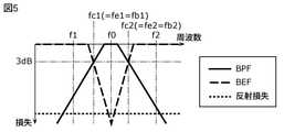
- FIG. 3 is a diagram showing the insertion loss characteristics of each filter shown in FIG.
- the horizontal axis represents frequency and the vertical axis represents insertion loss.
- the thick solid line in FIG. 3 represents the frequency characteristic of the insertion loss of the low-pass filter 30L.
- the thick dashed line represents the frequency characteristic of the insertion loss of the high-pass filter 40H.
- the thick dotted line represents the frequency characteristics of the reflection loss of the low-pass filter 30L and the high-pass filter 40H as seen from the node N3.
- the low-pass filter 30L passes a signal having a frequency fl or less and blocks a signal having a frequency fl or higher.
- the frequency fl is the corner frequency of the low-pass filter 30L.
- the low-pass filter 30L has a range of frequency fl or less as a pass band.
- the corner frequency is also called the cutoff frequency or cutoff frequency.
- the corner frequency corresponds to the frequency at which the insertion loss becomes about 3 dB in the frequency characteristic of the low-pass filter 30L.
- the corner frequency is also synonymous with the high-pass filter, band-pass filter, and band elimination filter described later.
- the high-pass filter 40H passes signals above the frequency fh and blocks signals below the frequency fh.
- the frequency fh is the corner frequency of the high-pass filter 40H.
- the high-pass filter 40H has a range of frequency fh or higher as a pass band.
- the low-pass filter 30L and the high-pass filter 40H have their respective pass bands complementary to each other.
- the corner frequency fl of the low-pass filter 30L is equal to the corner frequency fh of the high-pass filter 40H.
- "equal" not only means an exact match, but also includes a case where there is an error of about 10% or less. That is, the corner frequency fl of the low-pass filter 30L and the corner frequency fh of the high-pass filter 40H do not have to completely match, and can be regarded as substantially equal. The same applies to the case of the bandpass filter and the band elimination filter described later.
- the corner frequencies of the two filters are equal, the reflection loss when looking at the two filters from the node N3 is suppressed to be sufficiently small in the entire frequency band. Therefore, the signal input from the node N3 to the two filters passes through one of the two filters without being reflected by either of the two filters. That is, of the signals input from the combined output terminal 50 to the two filters via the node N3, the signal reflected by the two filters and returned from the combined output terminal 50 to the detector 2 is sufficiently suppressed.
- the fundamental frequency f0 is the frequency of the fundamental wave of the high frequency signal transmitted on the main line 10. That is, the fundamental frequency f0 is the frequency (that is, the target frequency) of the signal to be detected by the detector 2.
- the 2nd harmonic frequency 2f0 and the 3rd harmonic frequency 3f0 are frequencies of unnecessary signals that should not be input to the detector 2.
- the fundamental frequency f0 is included in the pass band (fl or less) of the low-pass filter 30L.
- the frequencies 2f0 and 3f0 are included in the pass band (fh or more) of the high-pass filter 40H.
- the desired signal (fundamental wave) having the fundamental frequency f0 passes through the low-pass filter 30L and is input to the detector 2 via the node N3 and the coupling output terminal 50.
- the detection accuracy of the detector 2 can be improved.
- the two filters 30 and 40 included in the directional coupler 1 are not limited to the example shown in FIG.
- the filters 30 and 40 may be a bandpass filter and a band elimination filter.
- FIG. 4 is a diagram showing another configuration example of a plurality of filters included in the directional coupler 1 according to the present embodiment.
- the bandpass filter 30B shown in FIG. 4 is an example of the filter 30 shown in FIG.
- the band elimination filter 40E is an example of the filter 40 shown in FIG.
- the bandpass filter 30B and the band elimination filter 40E constitute, for example, a diplexer.
- FIG. 5 is a diagram showing the insertion loss characteristics of each filter shown in FIG. In FIG. 4, the horizontal axis represents frequency and the vertical axis represents insertion loss.
- the thick solid line in FIG. 4 represents the frequency characteristic of the insertion loss of the bandpass filter 30B.
- the thick dashed line represents the frequency characteristic of the insertion loss of the band elimination filter 40E.
- the thick dotted line represents the frequency characteristic of the reflection loss of the bandpass filter 30B and the band elimination filter 40E as seen from the node N3.
- the bandpass filter 30B passes signals having a frequency of fb1 or more and fb2 or less, and blocks signals having a frequency of less than fb1 and signals having a frequency of more than fb2.
- the frequency fb1 is a corner frequency on the low frequency side of the bandpass filter 30B.
- the frequency fb2 is a corner frequency on the high frequency side of the bandpass filter 30B.
- the bandpass filter 30B has a range of fb1 or more and fb2 or less as a pass band.
- the band elimination filter 40E passes a signal having a frequency fe1 or less and a signal having a frequency fe2 or more, and blocks a signal larger than the frequency fe1 and less than the frequency fe2.
- the frequency fe1 is a corner frequency on the low frequency side of the band elimination filter 40E.
- the frequency fe2 is a corner frequency on the high frequency side of the band elimination filter 40E.
- the band elimination filter 40E has a range of frequency fe1 or less and a range of frequency fe2 or more as pass bands, respectively.
- One of the pass bands of the band elimination filter 40E (range of fe2 or more) is higher than the pass band of the bandpass filter 30B.
- the bandpass filter 30B and the band elimination filter 40E have their respective pass bands complementary to each other.
- the corner frequency fb1 of the bandpass filter 30B is equal to the corner frequency fe1 of the band elimination filter 40E.
- the corner frequency fb2 of the bandpass filter 30B is equal to the corner frequency fe2 of the band elimination filter 40E.
- the reflection loss when the two filters are viewed from the node N3 is suppressed to be sufficiently small in the entire frequency band. Therefore, of the signals input from the combined output terminal 50 to the two filters via the node N3, the signal reflected by the two filters and returned from the combined output terminal 50 to the detector 2 is sufficiently suppressed.
- the desired signal having the fundamental frequency f0 passes through the bandpass filter 30B and is input to the detector 2 via the node N3 and the coupled output terminal 50. Since unnecessary signals other than the fundamental wave do not substantially pass through the bandpass filter 30B, the detection accuracy of the detector 2 can be improved.
- the low-pass filter 30L, the high-pass filter 40H, the bandpass filter 30B, and the band elimination filter 40E are LC filters including at least one of a capacitor and an inductor, respectively.
- at least one of the low-pass filter 30L, the high-pass filter 40H, the band-pass filter 30B and the band elimination filter 40E may include a surface acoustic wave filter such as a SAW (Surface Acoustic Wave) filter or a BAW (Bulk Acoustic Wave) filter. ..
- at least one of the low-pass filter 30L, the high-pass filter 40H, the bandpass filter 30B, and the band elimination filter 40E may be a filter formed in an integrated passive device (IPD: Integrated Passive Device).
- IPD integrated Passive Device
- FIG. 6 is a diagram for explaining a signal flowing in the directional coupler 1x according to the comparative example.
- FIG. 7 is a diagram for explaining a signal flowing in the directional coupler 1 according to the present embodiment.
- the directional coupler 1x according to the comparative example is different from the directional coupler 1 according to the present embodiment in that it does not include the filter 40 and the termination circuit 60.
- a high frequency signal is transmitted from the input / output terminal 11 to the input / output terminal 12 on the main line 10.
- a part of the high frequency signal transmitted on the main line 10 flows through the sub line 20 as a coupled signal by electromagnetic coupling between the main line 10 and the sub line 20.
- the coupled signal includes a fundamental wave signal 90 having a fundamental frequency f0 of a high frequency signal and an unnecessary wave signal 91 other than the fundamental wave signal 90.
- the unwanted wave signal 91 is, for example, a distorted signal generated in a transmission circuit or the like.
- both the fundamental wave signal 90 and the unnecessary wave signal 91 are input to the filter 30 from one end 21 of the sub line 20 via the node N1. Since the filter 30 passes the fundamental wave signal 90, the fundamental wave signal 90 that has passed through the filter 30 is input to the detector 2. As a result, the detector 2 detects the fundamental wave signal 90.
- the unwanted wave signal 91 cannot pass through the filter 30 and is reflected by the filter 30. If the filter 30 is not provided and the unnecessary wave signal 91 is input to the detector 2, an error occurs in the power of the detected signal and the detection accuracy is lowered. On the other hand, in the directional couplers 1x and 1, since the unnecessary wave signal 91 is not input to the detector 2 by the filter 30, the detection accuracy in the detector 2 can be improved.
- the distortion signal 92 is generated.
- the distorted signal 92 corresponds to the harmonics of the fundamental wave signal 90. That is, the main frequency of the distorted signal 92 is a frequency twice or three times the fundamental frequency.
- the distortion signal 92 generated by the detector 2 returns to the filter 30 via the coupling output terminal 50. Since the distorted signal 92 is not included in the pass band of the filter 30, it is reflected by the filter 30 and returns to the detector 2 via the coupled output terminal 50. The distortion signal 92 returned to the detector 2 deteriorates the detection accuracy of the detector 2.
- the accuracy of the detector 2 cannot be improved due to the influence of the distortion signal 92.
- a filter 40 is connected to the coupling output terminal 50.
- the filter 40 is configured to pass the distorted signal 92 without passing the fundamental wave signal 90. Therefore, the distortion signal 92 input from the coupling output terminal 50 to the node N3 passes through the filter 40.
- the node N2 which is the other end of the filter 40, is terminated by the termination circuit 60. Specifically, since the impedance of the termination circuit 60 is adjusted so that the distortion signal 92 can be appropriately absorbed and consumed, the distortion signal 92 that has passed through the filter 40 is absorbed and consumed by the termination circuit 60.
- the directional coupler 1 As described above, in the directional coupler 1 according to the present embodiment, it is possible to suppress the distortion signal 92 from returning to the detector 2. Therefore, according to the directional coupler 1, the detection accuracy of the detector 2 can be improved.
- the directional coupler 1 has a main line 10, a sub line 20 that is electromagnetically coupled to the main line 10, and a coupling output terminal connected to one end 21 of the sub line 20.
- the 50 is provided with a filter 30 connected between one end 21 of the sub-line 20 and the coupling output terminal 50, and a filter 40 having a pass band higher than the pass band of the filter 30.
- One end of the filter 40 is connected to the coupling output terminal 50, and the other end of the filter 40 is terminated.
- the detector 2 when the detector 2 is connected to the coupled output terminal 50, the detector 2 can be made to input the fundamental wave signal 90 of the target frequency, and the unnecessary wave signal 91 is input. It can be suppressed by the filter 30. Further, since the distortion signal 92 generated by the detector 2 passes through the filter 40 and is absorbed and consumed, it is suppressed that the distortion signal 92 returns to the detector 2. As described above, the unnecessary wave signal 91 and the distorted signal 92 are less likely to be input to the detector 2, so that the detection accuracy can be improved.
- the distortion signal 92 since the distortion signal 92 does not pass through the filter 30, it is suppressed from being mixed into the main line 10 via the sub line 20. If the distortion signal 92 is mixed in the main line 10, there is a risk of causing unnecessary radiation from the antenna and obstacles to the transmitter operation such as the generation of intermodulation distortion. According to the directional coupler 1 according to the present embodiment, since the distortion signal 92 is suppressed from being mixed into the main line 10, it is possible to suppress the occurrence of obstacles to the transmitter operation.
- a circuit including a switch that causes a distortion signal to be generated and a plurality of filters are connected to the other end side of the sub line.
- the main difference is that it is done.
- the differences from the first embodiment will be mainly described, and the common points will be omitted or simplified.
- FIG. 8 is a diagram showing a configuration of a directional coupler 101 according to the present embodiment.
- the directional coupler 101 includes a variable terminating circuit 170 instead of the terminating circuit 70 as compared with the directional coupler 1 according to the first embodiment. Further, the directional coupler 101 includes a filter 130, a filter 140, a termination circuit 160, and a switch circuit 180.
- the filter 130 is an example of a third filter, and is connected between the other end 22 of the sub line 20 and the variable termination circuit 170.
- the node N4 which is one end of the filter 130, is connected to the other end 22 of the sub line 20.
- the node N6, which is the other end of the filter 130, is connected to the variable termination circuit 170. In this embodiment, the node N6 is connected to the variable termination circuit 170 via the switch circuit 180.
- the filter 130 has a predetermined pass band and is configured to allow a desired signal to pass through. Specifically, the filter 130 passes a signal having a target frequency detected by the detector 2.
- the filter 130 is a filter having the same pass band as the filter 30, but is not limited to this.
- the filter 130 may be a band-pass filter 30B.
- the filter 130 may be a lowpass filter 30L.
- the modifications applicable to the filter 30 are also applicable to the filter 130.
- the filter 140 is an example of the fourth filter, and is connected between the variable termination circuit 170 and the ground.
- the node N6, which is one end of the filter 140, is connected to the variable termination circuit 170.
- the node N5, which is the other end of the filter 140, is terminated. Specifically, the node N5 of the filter 140 is connected to the ground via the terminal circuit 160.
- the filter 140 has a pass band higher than the pass band of the filter 130. Specifically, the filter 140 passes a signal in the harmonic band of the target frequency detected by the detector 2.
- the pass band of the filter 140 may include a pass band higher than the pass band of the filter 130.
- the filter 140 may be a band pass filter or a high pass filter having a pass band higher than the pass band of the filter 130, or may be a band elimination filter that blocks only the pass band of the filter 130.
- the filter 140 is a filter having the same pass band as the filter 40, but is not limited to this.
- the filter 140 may be a band elimination filter 40E.
- the filter 140 may be a high-pass filter 40H.
- the modifications applicable to the filter 40 are also applicable to the filter 140.
- the termination circuit 160 is connected to the node N5 of the filter 140.
- the impedance of the termination circuit 160 is adjusted to a predetermined value so that the signal passing through the filter 140 can be absorbed and consumed. Specifically, the impedance of the termination circuit 160 is adjusted to an appropriate value so as to absorb and consume the distortion signals 94 and 95 (see FIG. 10) generated by the switch circuit 180 or the variable termination circuit 170.
- the variable termination circuit 170 is an example of a termination circuit connected to the other end 22 of the sub line 20.
- the variable termination circuit 170 is a termination circuit whose impedance can be changed.
- FIG. 9 is a circuit diagram showing an example of a variable termination circuit 170 included in the directional coupler 101 according to the present embodiment.
- the variable termination circuit 170 includes three resistors R1 to R3, three capacitors C1 to C3, six switches SW1 to SW6, and a terminal 171.
- the terminal 171 is connected to the other end 22 of the sub line 20.
- the terminal 171 is connected to the other end 22 of the sub line 20 via the filter 130 and the switch circuit 180.
- the resistors R1 to R3 and the capacitors C1 to C3 are connected in series with one of the six switches SW1 to SW6, respectively.
- a series circuit of the resistor and the switch and a series circuit of the capacitor and the switch are connected in parallel between the terminal 171 and the ground.
- the resistance values of the resistors R1 to R3 may be equal to or different from each other.
- the capacitance values of the capacitors C1 to C3 may be equal to or different from each other.
- the switch may not be connected to one of the three resistors R1 to R3.
- a switch may not be connected to one of the three capacitors C1 to C3.
- the switches SW1 to SW6 are switching elements such as MOSFETs (Metal Oxide Semiconductor Field Effect Transistor) and the like.
- the switches SW1 to SW6 can be switched on / off (conducting / non-conducting). This makes it possible to change the impedance of the variable termination circuit 170.
- the switches SW1 to SW6 are adjusted based on the fundamental frequency f0 of the high frequency signal transmitted on the main line 10.
- the on / off of the switches SW1 to SW6 is controlled so that the impedance of the variable termination circuit 170 becomes a value such that the signal of the fundamental frequency f0 can be sufficiently absorbed and consumed by the variable termination circuit 170.
- the variable termination circuit 170 may include one or more inductors. Further, the circuit configuration of the variable termination circuit 170 is not particularly limited. The variable termination circuit 170 may not include a resistor or a capacitor.
- the switch circuit 180 includes an example of a first switch circuit connected between the filter 30 and the coupling output terminal 50. Further, the switch circuit 180 includes an example of a second switch circuit connected between the filter 130 and the variable termination circuit 170.
- the switch circuit 180 has four terminals 181 to 184.
- Terminal 181 is connected to node N3.
- the terminal 182 is connected to the combined output terminal 50.
- Terminal 183 is connected to node N6.
- Terminal 184 is connected to the variable termination circuit 170.
- the node N3 which is the end of each of the filters 30 and 40, is connected to one of the coupled output terminal 50 and the variable termination circuit 170 via the switch circuit 180. Further, the node N6, which is the end of each of the filters 130 and 140, is connected to the other of the coupled output terminal 50 and the variable termination circuit 170 via the switch circuit 180.
- the switch circuit 180 one end 21 of the sub line 20 is connected to the coupling output terminal 50 via the filter 30, and the other end 22 of the sub line 20 is a variable termination circuit via the filter 130.
- the second connection state to connect to 170 is switched.
- the first connection state is a state in which the terminal 181 and the terminal 182 are connected (conducting), and the terminal 183 and the terminal 184 are connected (conducting).
- the second connection state is a state in which the terminal 181 and the terminal 184 are connected (conducting), and the terminal 183 and the terminal 182 are connected (conducting). Conduction and non-conduction between the terminals of the switch circuit 180 are switched by using a switching element such as a MOSFET.
- the end of the sub line 20 connected to the coupling output terminal 50 can be switched between one end 21 and the other end 22.
- This enables bidirectional detection in the detector 2. That is, the detector 2 can detect not only the fundamental wave signal 90 of the traveling wave but also the fundamental wave signal of the reflected wave.
- FIG. 10 is a diagram for explaining a signal flowing in the directional coupler 101 according to the present embodiment.
- the fundamental wave signal 90, the unnecessary wave signal 91, and the distorted wave signal 92 are the same as those in the first embodiment. Therefore, the directional coupler 101 according to the present embodiment can improve the detection accuracy as in the first embodiment.
- the reflected wave is taken out as a reflected wave coupling signal to the sub-line 20 by electromagnetic coupling between the main line 10 and the sub-line 20 in the same manner as the traveling wave.
- the reflected wave coupling signal includes a reflected wave fundamental wave signal 90r having a fundamental frequency f0.
- the reflected wave fundamental wave signal 90r is input to the filter 130 from the other end 22 of the sub line 20 via the node N4. Since the filter 130 passes the reflected wave fundamental wave signal 90r, the reflected wave fundamental wave signal 90r reaches the variable termination circuit 170 from the node N6 via the switch circuit 180. Since the impedance of the variable termination circuit 170 is adjusted so that the reflected wave fundamental wave signal 90r can be absorbed and consumed, the reflected wave fundamental wave signal 90r is absorbed and consumed by the variable termination circuit 170. Therefore, since the reflected wave fundamental wave signal 90r is suppressed from returning to the sub line 20 and reaching the coupled output terminal 50, it is possible to suppress a decrease in the detection accuracy of the detector 2. Further, since the reflected wave fundamental wave signal 90r is suppressed from returning to the main line 10 via the sub line 20, it is possible to suppress the occurrence of obstacles to the transmitter operation.
- variable termination circuit 170 and the switch circuit 180 include a switching element for switching between conduction and non-conduction of wiring.
- a constant distortion signal is generated.
- the switch circuit 180 generates distortion signals 93 and 94
- the variable termination circuit 170 generates distortion signals 95.
- the distorted signals 93 to 95 are, for example, signals having a frequency higher than the fundamental frequency f0.
- the distortion signal 93 is generated in the switch circuit 180 and flows toward the node N3. Since the distorted signal 93 is a signal having a frequency different from the fundamental frequency f0, it does not pass through the filter 30. Therefore, since the distortion signal 93 is suppressed from being mixed into the main line 10 via the sub line 20, it is possible to suppress the occurrence of a failure in the transmitter operation.
- the pass band of the filter 30 and the pass band of the filter 40 are in a complementary relationship, the distortion signal 93 that does not pass through the filter 30 passes through the filter 40 and is absorbed and consumed by the termination circuit 60. That is, since the distortion signal 93 is not reflected by the filters 30 and 40, it is suppressed from being input to the detector 2 via the switch circuit 180 and the coupling output terminal 50. Therefore, it is possible to suppress a decrease in detection accuracy.
- the distortion signal 94 is generated in the switch circuit 180 and flows toward the node N6. Since the distorted signal 94 is a signal having a frequency different from the fundamental frequency f0, it does not pass through the filter 130. Therefore, since the distortion signal 94 is suppressed from being mixed into the main line 10 via the sub line 20, it is possible to suppress the occurrence of a failure in the transmitter operation.
- the distortion signal 94 that does not pass through the filter 130 passes through the filter 140 and is absorbed and consumed by the termination circuit 160. That is, since the distortion signal 94 is not reflected by the filters 130 and 140, it can be prevented from affecting other circuits.
- the distortion signal 95 is generated in the variable termination circuit 170 and flows toward the node N6 via the switch circuit 180. Like the distortion signal 94, the distortion signal 95 passes through the filter 140 without passing through the filter 130, and is absorbed and consumed by the termination circuit 160. Therefore, it is possible to suppress the occurrence of a failure in the transmitter operation.
- the distortion signal 95 flows toward the node N3 depending on the connection state of the switch circuit 180.
- the distorted signal 95 like the distorted signal 93, passes through the filter 40 and is absorbed and consumed without passing through the filter 30. Therefore, in this case as well, it is possible to suppress the occurrence of a failure in the transmitter operation.
- the directional coupler 101 is connected between the terminal circuit connected to the other end 22 of the sub line 20 and the other end 22 of the sub line 20 and the terminal circuit. It comprises a filter 130 and a filter 140 having a pass band higher than the pass band of the filter 130. One end of the filter 140 is connected to the termination circuit and the other end of the filter 140 is terminated.
- the distortion signal generated on the other end 22 side of the sub line 20 does not pass through the filter 130, so that it is suppressed from being mixed into the main line 10 via the sub line 20. Therefore, it is possible to suppress the occurrence of a failure in the transmitter operation.
- the terminal circuit connected to the other end 22 is a variable terminal circuit 170 having a variable impedance.
- the distortion signal 95 generated in the variable termination circuit 170 passes through the filter 140 without passing through the filter 130, and is absorbed and consumed. Since the distortion signal 95 is suppressed from being mixed into the main line 10 via the sub line 20, it is possible to suppress the occurrence of a failure in the transmitter operation.
- the directional coupler 101 further includes a first switch circuit connected between the filter 30 and the coupling output terminal 50.
- One end of the filter 40 is connected to the coupling output terminal 50 via the first switch circuit.
- the distortion signal 93 generated in the switch circuit 180 passes through the filter 40 and is absorbed and consumed without passing through the filter 30. Since the distortion signal 93 is suppressed from being mixed into the main line 10 via the sub line 20, it is possible to suppress the occurrence of a failure in the transmitter operation. Further, since the distortion signal 93 is not reflected by the filters 30 and 40, it is suppressed from being input to the detector 2. Therefore, it is possible to suppress a decrease in the detection accuracy of the detector 2.
- the directional coupler 101 further includes a second switch circuit connected between the filter 130 and the termination circuit. One end of the filter 140 is connected to the termination circuit via the second switch circuit.
- the distortion signal 94 generated in the switch circuit 180 passes through the filter 140 and is absorbed and consumed without passing through the filter 130. Since the distortion signal 94 is suppressed from being mixed into the main line 10 via the sub line 20, it is possible to suppress the occurrence of a failure in the transmitter operation.
- the directional coupler 101 does not have to include the switch circuit 180. Further, the directional coupler 101 may include a terminal circuit 70 having a fixed impedance instead of the variable terminal circuit 170.
- the directional coupler according to the third embodiment is different from the second embodiment in that each of both ends of the sub line is provided with a filter whose other end is terminated.
- the differences from the second embodiment will be mainly described, and the common points will be omitted or simplified.
- FIG. 11 is a diagram showing a configuration of a directional coupler 201 according to the present embodiment.
- the directional coupler 201 further comprises filters 240 and 241 and termination circuits 260 and 261 as compared to the directional coupler 101 according to the second embodiment.
- the filter 240 is an example of the sixth filter, and is connected between one end 21 of the sub line 20 and the ground. One end of the filter 240 is connected to a path connecting one end 21 of the sub line 20 and the filter 30. The other end of the filter 240 is terminated. Specifically, the other end of the filter 240 is connected to the ground via the termination circuit 260.
- the filter 240 has a pass band different from the pass band of the filter 30. Specifically, the filter 240 passes a signal in the harmonic band of the target frequency detected by the detector 2.
- the pass band of the filter 240 and the pass band of the filter 30 are in a complementary relationship.
- the filter 240 is a filter having the same pass band as the filter 40, but is not limited to this.
- the filter 240 may be a band elimination filter 40E.
- the filter 240 may be a high-pass filter 40H.
- the filter 241 is an example of the fifth filter, and is connected between the other end 22 of the sub line 20 and the ground. One end of the filter 241 is connected to a path connecting the other end 22 of the sub line 20 and the filter 130. The other end of the filter 241 is terminated. Specifically, the other end of the filter 241 is connected to the ground via the termination circuit 261.
- the filter 241 has a pass band different from the pass band of the filter 130. Specifically, the filter 241 passes a signal in the harmonic band of the target frequency detected by the detector 2.
- the pass band of the filter 241 and the pass band of the filter 130 are in a complementary relationship.
- the filter 241 is a filter having the same pass band as the filter 140, but is not limited to this.
- the filter 241 may be a band elimination filter 40E.
- the filter 241 may be a high-pass filter 40H.
- the termination circuit 260 is connected to the other end of the filter 240.
- the impedance of the termination circuit 260 is adjusted to a predetermined value so that the signal passing through the filter 240 can be absorbed and consumed.
- the impedance of the terminal circuit 260 is adjusted to an appropriate value so as to absorb and consume the unnecessary wave signal 91 (see FIG. 12) flowing through the sub line 20 by electromagnetic coupling with the main line 10. ing.
- the termination circuit 261 is connected to the other end of the filter 241.
- the impedance of the termination circuit 261 is adjusted to a predetermined value so that the signal passing through the filter 241 can be absorbed and consumed.
- the impedance of the terminal circuit 261 is set to an appropriate value so as to absorb and consume the reflected wave unnecessary wave signal 91r (see FIG. 12) flowing through the sub line 20 by electromagnetic coupling with the main line 10. It has been adjusted.
- FIG. 12 is a diagram for explaining a signal flowing in the directional coupler 201 according to the present embodiment.
- the fundamental wave signal 90, the reflected wave fundamental wave signal 90r, and the distorted waves 92 to 95 are the same as those in the second embodiment. Therefore, the directional coupler 201 according to the present embodiment can improve the detection accuracy and suppress the occurrence of obstacles to the transmitter operation, as in the second embodiment.
- a filter 240 for passing a signal having a frequency different from the fundamental frequency f0 is connected to one end 21 of the sub line 20. Therefore, the unnecessary wave signal 91 passes through the filter 240 and is absorbed and consumed by the terminal circuit 260.
- a filter 241 for passing a signal having a frequency different from the fundamental frequency f0 is connected to the other end 22 of the sub line 20. Therefore, the reflected wave unnecessary wave signal 91r passes through the filter 241 and is absorbed and consumed by the terminal circuit 261.
- both the unnecessary wave signal 91 and the reflected wave unnecessary wave signal 91r are difficult to return to the sub line 20, so that they are suppressed from being mixed into the main line 10 via the sub line 20. Therefore, it is possible to suppress the occurrence of a failure in the transmitter operation.
- the directional coupler 201 includes a filter 241 having a pass band different from the pass band of the filter 130.
- One end of the filter 241 is connected to a path connecting the other end 22 of the sub line 20 and the filter 130, and the other end of the filter 241 is terminated.
- the directional coupler 201 further includes a filter 240 having a pass band different from the pass band of the filter 30.
- One end of the filter 240 is connected to a path connecting one end 21 of the sub line 20 and the filter 30, and the other end of the filter 240 is terminated.
- the directional coupler 201 may include only one of the filters 240 and 241.
- FIG. 13 is a diagram showing a modified example of the configuration of a plurality of filters included in the directional coupler 1, 101 or 201.
- FIG. 13 discloses an example in which each of the low-pass filter 30L, the band-pass filter 40B, and the high-pass filter 40H is connected to the node N3 (that is, the coupling output terminal 50).
- the bandpass filter 40B and the highpass filter 40H are examples of the second filter, respectively.
- the node N21, which is the other end of the bandpass filter 40B, is terminated. Specifically, the node N21 of the bandpass filter 40B is connected to the ground via the terminal circuit 60. Further, the node N22, which is the other end of the high-pass filter 40H, is also terminated. Specifically, the node N22 of the high-pass filter 40H is connected to the ground via the terminal circuit 61.
- the low-pass filter 30L, the band-pass filter 40B, and the high-pass filter 40H constitute, for example, a triplexer.
- the pass band of the low-pass filter 30L, the pass band of the band-pass filter 40B, and the pass band of the high-pass filter 40H have a complementary relationship with each other. That is, these three filters are configured so that the signal flowing from the node N3 toward the filter passes through one of the three filters and not the other two in the entire frequency band. There is.
- the impedances of the terminal circuits 60 and 61 are different from each other.
- the impedance of the terminal circuit 60 is adjusted so that a signal having a frequency of 2f0, which is a second harmonic of the fundamental frequency f0, can be appropriately absorbed and consumed.
- the impedance of the terminal circuit 61 is adjusted so that a signal having a frequency of 3f0, which is a third harmonic of the fundamental frequency f0, or a signal having a frequency higher than that can be appropriately absorbed and consumed.
- the impedance of the termination circuit 60 is adjusted so that the distortion signal 92 generated by the detector 2 can be appropriately absorbed and consumed, and the impedance of the termination circuit 61 appropriately matches the distortion signal 93 generated by the switch circuit 180. It may be adjusted so that it can be absorbed and consumed. Even when the frequencies of the distorted signals 92 and 93 are different, each of them can be appropriately absorbed and consumed.
- the directional coupler 1, 101 or 201 may include a plurality of filters 40.
- the filter configuration shown in FIG. 13 may be applied to the configurations of the filters 130 and 140 connected to the variable termination circuit 170 or the switch circuit 180. That is, the directional coupler 1, 101 or 201 may include a plurality of filters 140.
- the nodes N1 and N3 shown in FIG. 13 correspond to the nodes N4 and N6, respectively.
- the low-pass filter 30L is an example of the filter 130
- the band-pass filter 40B and the high-pass filter 40H are examples of the filter 140, respectively.
- the distortion signal generated on the other end 22 side of the sub line 20 is suppressed from returning to the main line 10, so that it is possible to suppress the occurrence of a failure in the transmitter operation.
- the combination of the three filters is not limited to the example shown in FIG.
- it may be three filters selected from a low-pass filter, a high-pass filter, a band-pass filter, and a band elimination filter.
- the three filters may include filters of the same type. Further, three or more terminated filters (second filter or fourth filter) may be provided.
- the directional coupler 1, 101 or 201 does not have to include the termination circuit 60.
- the filter 40 can be brought into a state equivalent to the termination of the other end of the filter 40.
- the directional coupler 101 or 201 may not include termination circuits 160, 260 or 261.
- the termination circuit 61 shown in FIG. 13 may not be provided.
- At least one of the low-pass filter 30L, the high-pass filter 40H, the band-pass filter 30B, and the band elimination filter 40E may be tuneable. That is, at least one of the low-pass filter 30L, the high-pass filter 40H, the band-pass filter 30B, and the band elimination filter 40E may have a changeable pass band.
- a switch or a varicap is used for tuning.
- the filter 30 may be composed only of an inductor connected in series between the node N1 and the node N3.
- the filter 40 may be composed of only a capacitor connected in series between the node N2 and the node N3.
- the filter 130 may consist only of an inductor connected in series between the node N4 and the node N6.
- the filter 140 may be composed of only a capacitor connected in series between the node N5 and the node N6.
- the directional coupler 1, 101 or 201 may include a detector 2.
- the directional coupler 1, 101 or 201 may include a plurality of main lines 10 or a plurality of sub lines 20.
- the plurality of sub-lines 20 may be electromagnetically coupled to one main line 10.
- the plurality of sub-lines 20 may be electromagnetically coupled to each of the plurality of main lines 10 on a one-to-one basis or a plurality of one-to-one basis.
- the directional coupler 1, 101 or 201 may include a line changeover switch for selecting a plurality of sub lines 20.
- the present invention can be widely used in electronic devices including directional couplers and communication devices.
Abstract
A directional coupler (1) is provided with a main line (10), a sub-line (20) electromagnetically coupled with the main line (10), a coupled output terminal (50) connected to one end (21) of the sub-line (20), a filter (30) connected between one end (21) of the sub-line (20) and the coupled output terminal (50), and a filter (40) having a passband higher than a passband of the filter (30). One end of the filter (40) is connected to the coupled output terminal. The other end of the filter (40) is terminated.
Description
本発明は、方向性結合器に関する。
The present invention relates to a directional coupler.
例えば、特許文献1には、主線路と副線路とを備える方向性結合器が開示されている。方向性結合器の副線路とカップリングポートとの間には、複数のフィルタを含む可変フィルタ回路が接続されている。
For example, Patent Document 1 discloses a directional coupler including a main line and a sub line. A variable filter circuit including a plurality of filters is connected between the sub line of the directional coupler and the coupling port.
上記従来の方向性結合器では、所望の信号のみを通過させるフィルタを利用することにより、カップリングポートから所望の信号をある程度は精度良く取り出すことができる。しかしながら、カップリングポートに検波器が接続された場合、検波器では、入力された所望の信号の高調波などの歪成分が発生する。歪成分は、カップリングポートを介してフィルタに戻り、フィルタによって反射される。フィルタによって反射された歪成分は、再び検波器に入力されて、検波精度を悪化させる。
In the above-mentioned conventional directional coupler, the desired signal can be extracted from the coupling port with a certain degree of accuracy by using a filter that allows only the desired signal to pass through. However, when a detector is connected to the coupling port, the detector generates distortion components such as harmonics of the input desired signal. The strain component returns to the filter through the coupling port and is reflected by the filter. The distortion component reflected by the filter is input to the detector again, and the detection accuracy is deteriorated.
そこで、本発明は、検波器が接続された場合に、接続された検波器の検波精度を向上させることができる方向性結合器を提供することを目的とする。
Therefore, an object of the present invention is to provide a directional coupler capable of improving the detection accuracy of the connected detector when the detector is connected.
本発明の一態様に係る方向性結合器は、主線路と、主線路と電磁気的に結合する副線路と、副線路の一端に接続された出力端子と、副線路の一端と出力端子との間に接続された第1フィルタと、第1フィルタの通過帯域より高い通過帯域を有する第2フィルタと、を備え、第2フィルタの一端は、出力端子に接続され、第2フィルタの他端は、終端されている。
The directional coupler according to one aspect of the present invention includes a main line, a sub line electromagnetically coupled to the main line, an output terminal connected to one end of the sub line, and one end and an output terminal of the sub line. A first filter connected in between and a second filter having a pass band higher than the pass band of the first filter are provided, one end of the second filter is connected to an output terminal, and the other end of the second filter is connected. , Terminated.
本発明に係る方向性結合器によれば、検波器が接続された場合に、接続された検波器の検波精度を向上させることができる。
According to the directional coupler according to the present invention, when a detector is connected, the detection accuracy of the connected detector can be improved.
以下では、本発明の実施の形態に係る方向性結合器について、図面を用いて詳細に説明する。なお、以下に説明する実施の形態は、いずれも本発明の一具体例を示すものである。したがって、以下の実施の形態で示される数値、形状、材料、構成要素、構成要素の配置、接続形態、ステップ及びステップの順序などは、一例であり、本発明を限定する趣旨ではない。よって、以下の実施の形態における構成要素のうち、独立請求項に記載されていない構成要素については、任意の構成要素として説明される。
Hereinafter, the directional coupler according to the embodiment of the present invention will be described in detail with reference to the drawings. In addition, all of the embodiments described below show a specific example of the present invention. Therefore, the numerical values, shapes, materials, components, arrangement of components, connection modes, steps, order of steps, etc. shown in the following embodiments are examples, and are not intended to limit the present invention. Therefore, among the components in the following embodiments, the components not described in the independent claims are described as arbitrary components.
また、各図は、模式図であり、必ずしも厳密に図示されたものではない。したがって、例えば、各図において縮尺などは必ずしも一致しない。また、各図において、実質的に同一の構成については同一の符号を付しており、重複する説明は省略又は簡略化する。
Also, each figure is a schematic diagram and is not necessarily exactly illustrated. Therefore, for example, the scales and the like do not always match in each figure. Further, in each figure, substantially the same configuration is designated by the same reference numeral, and duplicate description will be omitted or simplified.
また、本明細書において、一致及び等しいなどの要素間の関係性を示す用語、並びに、数値範囲は、厳格な意味のみを表す表現ではなく、実質的に同等な範囲、例えば数%程度の差異をも含むことを意味する表現である。
Further, in the present specification, terms indicating relationships between elements such as match and equality, and numerical ranges are not expressions that express only strict meanings, but substantially equivalent ranges, for example, differences of about several percent. It is an expression that means to include.
また、本発明の回路構成の説明において、「直接接続される」とは、他の回路素子を介さずに接続端子及び/又は配線導体で直接接続されることを意味する。一方、「接続される」とは、接続端子及び配線導体で直接接続される場合だけでなく、他の回路素子を介して電気的に接続される場合も含む。また、「AとBとの間に接続される」とは、AとBとの間でA及びBの両方に接続されることを意味する。
Further, in the description of the circuit configuration of the present invention, "directly connected" means that the circuit is directly connected by a connection terminal and / or a wiring conductor without using other circuit elements. On the other hand, the term "connected" includes not only the case of being directly connected by a connection terminal and a wiring conductor, but also the case of being electrically connected via another circuit element. Further, "connected between A and B" means that both A and B are connected between A and B.
(実施の形態1)
[1-1.構成]
まず、実施の形態1に係る方向性結合器の構成について、図1を用いて説明する。図1は、本実施の形態に係る方向性結合器1の構成を示す図である。 (Embodiment 1)
[1-1. composition]
First, the configuration of the directional coupler according to the first embodiment will be described with reference to FIG. FIG. 1 is a diagram showing a configuration of adirectional coupler 1 according to the present embodiment.
[1-1.構成]
まず、実施の形態1に係る方向性結合器の構成について、図1を用いて説明する。図1は、本実施の形態に係る方向性結合器1の構成を示す図である。 (Embodiment 1)
[1-1. composition]
First, the configuration of the directional coupler according to the first embodiment will be described with reference to FIG. FIG. 1 is a diagram showing a configuration of a
図1に示されるように、方向性結合器1は、主線路10と、副線路20と、フィルタ30と、フィルタ40と、結合出力端子50と、終端回路60及び70と、を備える。方向性結合器1は、主線路10を伝送される高周波信号を検波器2で検出させるために設けられている。
As shown in FIG. 1, the directional coupler 1 includes a main line 10, a sub line 20, a filter 30, a filter 40, a coupling output terminal 50, and termination circuits 60 and 70. The directional coupler 1 is provided so that the detector 2 can detect a high frequency signal transmitted through the main line 10.
主線路10は、2つの入出力端子11及び12を有する。入出力端子11は、送信用の高周波信号を生成する送信回路、及び、アンテナで受信された高周波信号を処理する受信回路の少なくとも一方に接続される。入出力端子12は、アンテナに接続される。なお、入出力端子11がアンテナに接続され、入出力端子12が送信回路又は受信回路に接続されてもよい。
The main line 10 has two input / output terminals 11 and 12. The input / output terminal 11 is connected to at least one of a transmission circuit that generates a high frequency signal for transmission and a reception circuit that processes the high frequency signal received by the antenna. The input / output terminal 12 is connected to the antenna. The input / output terminal 11 may be connected to the antenna, and the input / output terminal 12 may be connected to the transmission circuit or the reception circuit.
副線路20は、主線路10と電磁気的に結合している。副線路20は、一端21及び他端22を有する。一端21は、フィルタ30を介して結合出力端子50に接続されている。他端22は、終端回路70に接続されている。
The sub line 20 is electromagnetically coupled to the main line 10. The auxiliary line 20 has one end 21 and the other end 22. One end 21 is connected to the combined output terminal 50 via a filter 30. The other end 22 is connected to the terminal circuit 70.
フィルタ30は、第1フィルタの一例であり、副線路20の一端21と結合出力端子50との間に接続されている。フィルタ30の一端であるノードN1は、副線路20の一端21に接続されている。フィルタ30の他端であるノードN3は、結合出力端子50に接続されている。
The filter 30 is an example of the first filter, and is connected between one end 21 of the sub line 20 and the coupling output terminal 50. The node N1 which is one end of the filter 30 is connected to one end 21 of the sub line 20. The node N3, which is the other end of the filter 30, is connected to the combined output terminal 50.
フィルタ30は、所定の通過帯域を有し、所望の信号が通過可能に構成されている。具体的には、フィルタ30は、検波器2で検出する目的周波数の信号を通過させる。
The filter 30 has a predetermined pass band and is configured to allow a desired signal to pass through. Specifically, the filter 30 passes a signal having a target frequency detected by the detector 2.
フィルタ40は、第2フィルタの一例であり、結合出力端子50とグランドとの間に接続されている。フィルタ40の一端であるノードN3は、結合出力端子50に接続されている。フィルタ40の他端であるノードN2は、終端されている。具体的には、フィルタ40のノードN2は、終端回路60を介してグランドに接続されている。
The filter 40 is an example of the second filter, and is connected between the coupling output terminal 50 and the ground. The node N3, which is one end of the filter 40, is connected to the combined output terminal 50. The node N2, which is the other end of the filter 40, is terminated. Specifically, the node N2 of the filter 40 is connected to the ground via the terminal circuit 60.
フィルタ40は、フィルタ30の通過帯域より高い通過帯域を有する。具体的には、フィルタ40は、検波器2で検出する目的周波数の高調波帯の信号を通過させる。なお、フィルタ40の通過帯域には、フィルタ30の通過帯域より高い通過帯域が含まれていればよい。フィルタ40は、後述するように、フィルタ30の通過帯域より高い通過帯域を有するバンドパスフィルタまたはハイパスフィルタであってもよいし、フィルタ30の通過帯域のみを遮断するようなバンドエリミネイションフィルタであってもよい。
The filter 40 has a pass band higher than the pass band of the filter 30. Specifically, the filter 40 passes a signal in the harmonic band of the target frequency detected by the detector 2. The pass band of the filter 40 may include a pass band higher than the pass band of the filter 30. As will be described later, the filter 40 may be a bandpass filter or a highpass filter having a passband higher than the passband of the filter 30, or a band elimination filter that blocks only the passband of the filter 30. You may.
フィルタ30及び40は、ダイプレクサを構成していてもよい。この場合、ノードN3がダイプレクサの共通端子であり、ノードN1及びN2がそれぞれ、分波入出力端子である。ダイプレクサでは、各分波入出力端子を通過できる周波数帯域は、例えば、互いに相補関係にある。フィルタ30及び40の具体的な構成及び周波数特性の例については、後で説明する。
The filters 30 and 40 may constitute a diplexer. In this case, the node N3 is a common terminal of the diplexer, and the nodes N1 and N2 are demultiplexing input / output terminals, respectively. In the diplexer, the frequency bands that can pass through each demultiplexing input / output terminal are, for example, complementary to each other. Specific configurations of the filters 30 and 40 and examples of frequency characteristics will be described later.
結合出力端子50は、「出力端子」の一例であり、副線路20の一端21に接続されている。具体的には、結合出力端子50は、フィルタ30を介して副線路20の一端21に接続されている。また、結合出力端子50には、フィルタ40及び終端回路60を介してグランドに接続されている。結合出力端子50には、検波器2が接続される。
The combined output terminal 50 is an example of an "output terminal" and is connected to one end 21 of the sub line 20. Specifically, the coupling output terminal 50 is connected to one end 21 of the sub line 20 via the filter 30. Further, the coupling output terminal 50 is connected to the ground via the filter 40 and the termination circuit 60. The detector 2 is connected to the coupled output terminal 50.
終端回路60は、フィルタ40のノードN2に接続されている。終端回路60のインピーダンスは、フィルタ40を通過する信号を吸収消費できるように、所定の値に調整されている。具体的には、終端回路60のインピーダンスは、検波器2で発生する歪信号92(図7を参照)を吸収消費するように、適切な値に調整されている。
The termination circuit 60 is connected to the node N2 of the filter 40. The impedance of the termination circuit 60 is adjusted to a predetermined value so that the signal passing through the filter 40 can be absorbed and consumed. Specifically, the impedance of the terminal circuit 60 is adjusted to an appropriate value so as to absorb and consume the distortion signal 92 (see FIG. 7) generated by the detector 2.
終端回路70は、副線路20の他端22に接続されている。終端回路70のインピーダンスは、主線路10を伝送される高周波信号のうち、入出力端子12から入出力端子11へと反射した基本周波数f0の信号を吸収消費できるように、所定の値に調整されている。終端回路70は、例えば50Ω抵抗器である。
The terminal circuit 70 is connected to the other end 22 of the sub line 20. The impedance of the termination circuit 70 is adjusted to a predetermined value so that the signal of the fundamental frequency f0 reflected from the input / output terminal 12 to the input / output terminal 11 can be absorbed and consumed among the high frequency signals transmitted through the main line 10. ing. The termination circuit 70 is, for example, a 50Ω resistor.
以上のように構成された方向性結合器1は、主線路10を伝送される高周波信号の検波に利用される。高周波信号は、例えば、Wi-Fi(登録商標)、LTE(Long Term Evolution)又は5G(5th Generation)などの通信規格に準拠した信号である。方向性結合器1は、例えば、マルチモード/マルチバンド対応の携帯電話のフロントエンド部に配置される。
The directional coupler 1 configured as described above is used for detecting a high frequency signal transmitted on the main line 10. The high frequency signal is a signal compliant with a communication standard such as Wi-Fi (registered trademark), LTE (Long Term Evolution) or 5G (5th Generation). The directional coupler 1 is arranged, for example, in the front end portion of a multimode / multiband compatible mobile phone.
主線路10を伝送される高周波信号の一部は、副線路20、フィルタ30及び結合出力端子50を介して検波器2に入力される。検波器2は、入力される信号の信号電力などを検出し、検出結果を検波結果出力端子3から出力する。
A part of the high frequency signal transmitted on the main line 10 is input to the detector 2 via the sub line 20, the filter 30, and the coupling output terminal 50. The detector 2 detects the signal power of the input signal and outputs the detection result from the detection result output terminal 3.
検波結果出力端子3は、例えば、送信回路若しくは受信回路又はこれらの回路の制御回路に接続される。これにより、例えば、送信回路又は受信回路が備える増幅器の増幅率を制御することができる。検波精度を向上させることで、各種制御の精度及び信頼性を向上させることができる。
The detection result output terminal 3 is connected to, for example, a transmission circuit or a reception circuit or a control circuit of these circuits. Thereby, for example, the amplification factor of the amplifier provided in the transmission circuit or the reception circuit can be controlled. By improving the detection accuracy, the accuracy and reliability of various controls can be improved.
[1-2.フィルタの構成及び周波数特性]
次に、フィルタ30及び40の具体的な構成及び周波数特性の例について、図2及び図3を用いて説明する。 [1-2. Filter configuration and frequency characteristics]
Next, specific configurations of the filters 30 and 40 and examples of frequency characteristics will be described with reference to FIGS. 2 and 3.
次に、フィルタ30及び40の具体的な構成及び周波数特性の例について、図2及び図3を用いて説明する。 [1-2. Filter configuration and frequency characteristics]
Next, specific configurations of the
図2は、本実施の形態に係る方向性結合器1が備える複数のフィルタの構成例を示す図である。図2に示されるローパスフィルタ30Lは、図1に示されるフィルタ30の一例である。ハイパスフィルタ40Hは、図1に示されるフィルタ40の一例である。ローパスフィルタ30L及びハイパスフィルタ40Hは、例えば、ダイプレクサを構成している。
FIG. 2 is a diagram showing a configuration example of a plurality of filters included in the directional coupler 1 according to the present embodiment. The low-pass filter 30L shown in FIG. 2 is an example of the filter 30 shown in FIG. The high-pass filter 40H is an example of the filter 40 shown in FIG. The low-pass filter 30L and the high-pass filter 40H constitute, for example, a diplexer.
図3は、図2に示される各フィルタの挿入損失特性を示す図である。図3において、横軸は周波数を表し、縦軸は挿入損失を表している。図3の太実線は、ローパスフィルタ30Lの挿入損失の周波数特性を表している。太破線は、ハイパスフィルタ40Hの挿入損失の周波数特性を表している。太点線は、ノードN3から見たローパスフィルタ30L及びハイパスフィルタ40Hの反射損失の周波数特性を表している。
FIG. 3 is a diagram showing the insertion loss characteristics of each filter shown in FIG. In FIG. 3, the horizontal axis represents frequency and the vertical axis represents insertion loss. The thick solid line in FIG. 3 represents the frequency characteristic of the insertion loss of the low-pass filter 30L. The thick dashed line represents the frequency characteristic of the insertion loss of the high-pass filter 40H. The thick dotted line represents the frequency characteristics of the reflection loss of the low-pass filter 30L and the high-pass filter 40H as seen from the node N3.
図3に示されるように、ローパスフィルタ30Lは、周波数fl以下の信号を通過させ、周波数flより大きい信号を遮断する。周波数flは、ローパスフィルタ30Lのコーナー周波数である。ローパスフィルタ30Lは、周波数fl以下の範囲を通過帯域として有する。
As shown in FIG. 3, the low-pass filter 30L passes a signal having a frequency fl or less and blocks a signal having a frequency fl or higher. The frequency fl is the corner frequency of the low-pass filter 30L. The low-pass filter 30L has a range of frequency fl or less as a pass band.
コーナー周波数は、遮断周波数又はカットオフ周波数とも呼ばれる。コーナー周波数は、ローパスフィルタ30Lの周波数特性において、挿入損失が約3dBになるときの周波数に対応する。なお、コーナー周波数は、後述するハイパスフィルタ、バンドパスフィルタ及びバンドエリミネイションフィルタにおいても同義である。
The corner frequency is also called the cutoff frequency or cutoff frequency. The corner frequency corresponds to the frequency at which the insertion loss becomes about 3 dB in the frequency characteristic of the low-pass filter 30L. The corner frequency is also synonymous with the high-pass filter, band-pass filter, and band elimination filter described later.
ハイパスフィルタ40Hは、周波数fh以上の信号を通過させ、周波数fh未満の信号を遮断する。周波数fhは、ハイパスフィルタ40Hのコーナー周波数である。ハイパスフィルタ40Hは、周波数fh以上の範囲を通過帯域として有する。
The high-pass filter 40H passes signals above the frequency fh and blocks signals below the frequency fh. The frequency fh is the corner frequency of the high-pass filter 40H. The high-pass filter 40H has a range of frequency fh or higher as a pass band.
本実施の形態では、ローパスフィルタ30Lとハイパスフィルタ40Hとは、各々の通過帯域が互いに相補関係にある。具体的には、ローパスフィルタ30Lのコーナー周波数flは、ハイパスフィルタ40Hのコーナー周波数fhに等しい。ここで、「等しい」とは、完全な一致を意味するだけでなく、約10%以内の誤差がある場合も含んでいる。すなわち、ローパスフィルタ30Lのコーナー周波数flと、ハイパスフィルタ40Hのコーナー周波数fhとは、完全に一致していなくてもよく、実質的に等しいとみなせることができればよい。後述するバンドパスフィルタ及びバンドエリミネイションフィルタの場合についても同様である。
In the present embodiment, the low-pass filter 30L and the high-pass filter 40H have their respective pass bands complementary to each other. Specifically, the corner frequency fl of the low-pass filter 30L is equal to the corner frequency fh of the high-pass filter 40H. Here, "equal" not only means an exact match, but also includes a case where there is an error of about 10% or less. That is, the corner frequency fl of the low-pass filter 30L and the corner frequency fh of the high-pass filter 40H do not have to completely match, and can be regarded as substantially equal. The same applies to the case of the bandpass filter and the band elimination filter described later.
2つのフィルタのコーナー周波数が等しいので、ノードN3から2つのフィルタを見たときの反射損失は、全周波数帯域において十分に小さく抑制されている。このため、ノードN3から2つのフィルタに入力される信号は、2つのフィルタのいずれかで反射されることなく、2つのフィルタのいずれかを通過する。つまり、結合出力端子50からノードN3を介して2つのフィルタに入力する信号のうち、2つのフィルタによって反射されて再び結合出力端子50から検波器2に戻る信号が十分に抑制される。
Since the corner frequencies of the two filters are equal, the reflection loss when looking at the two filters from the node N3 is suppressed to be sufficiently small in the entire frequency band. Therefore, the signal input from the node N3 to the two filters passes through one of the two filters without being reflected by either of the two filters. That is, of the signals input from the combined output terminal 50 to the two filters via the node N3, the signal reflected by the two filters and returned from the combined output terminal 50 to the detector 2 is sufficiently suppressed.
図3に示されるように、2つのフィルタのコーナー周波数fc(=fl=fh)は、基本周波数f0より大きく、2倍高調波の周波数2f0より小さい。基本周波数f0は、主線路10を伝送される高周波信号の基本波の周波数である。つまり、基本周波数f0は、検波器2によって検波されるべき信号の周波数(すなわち、目的周波数)である。一方で、2倍高調波の周波数2f0及び3倍高調波の周波数3f0は、検波器2には入力されるべきではない不要な信号の周波数である。基本周波数f0は、ローパスフィルタ30Lの通過帯域(fl以下)に含まれている。周波数2f0及び3f0は、ハイパスフィルタ40Hの通過帯域(fh以上)に含まれている。
As shown in FIG. 3, the corner frequency fc (= fl = fh) of the two filters is larger than the fundamental frequency f0 and smaller than the frequency 2f0 of the second harmonic. The fundamental frequency f0 is the frequency of the fundamental wave of the high frequency signal transmitted on the main line 10. That is, the fundamental frequency f0 is the frequency (that is, the target frequency) of the signal to be detected by the detector 2. On the other hand, the 2nd harmonic frequency 2f0 and the 3rd harmonic frequency 3f0 are frequencies of unnecessary signals that should not be input to the detector 2. The fundamental frequency f0 is included in the pass band (fl or less) of the low-pass filter 30L. The frequencies 2f0 and 3f0 are included in the pass band (fh or more) of the high-pass filter 40H.
これにより、ノードN1から入力される高周波信号のうち、基本周波数f0の所望な信号(基本波)は、ローパスフィルタ30Lを通過し、ノードN3及び結合出力端子50を介して検波器2に入力される。基本波以外の不要な信号は、ローパスフィルタ30Lを実質的に通過しないので、検波器2の検波精度を向上させることができる。
As a result, among the high frequency signals input from the node N1, the desired signal (fundamental wave) having the fundamental frequency f0 passes through the low-pass filter 30L and is input to the detector 2 via the node N3 and the coupling output terminal 50. To. Since unnecessary signals other than the fundamental wave do not substantially pass through the low-pass filter 30L, the detection accuracy of the detector 2 can be improved.
なお、方向性結合器1が備える2つのフィルタ30及び40は、図2に示される例に限定されない。例えば、フィルタ30及び40は、バンドパスフィルタとバンドエリミネイションフィルタとであってもよい。
The two filters 30 and 40 included in the directional coupler 1 are not limited to the example shown in FIG. For example, the filters 30 and 40 may be a bandpass filter and a band elimination filter.
図4は、本実施の形態に係る方向性結合器1が備える複数のフィルタの別の構成例を示す図である。図4に示されるバンドパスフィルタ30Bは、図1に示されるフィルタ30の一例である。バンドエリミネイションフィルタ40Eは、図1に示されるフィルタ40の一例である。バンドパスフィルタ30B及びバンドエリミネイションフィルタ40Eは、例えば、ダイプレクサを構成している。
FIG. 4 is a diagram showing another configuration example of a plurality of filters included in the directional coupler 1 according to the present embodiment. The bandpass filter 30B shown in FIG. 4 is an example of the filter 30 shown in FIG. The band elimination filter 40E is an example of the filter 40 shown in FIG. The bandpass filter 30B and the band elimination filter 40E constitute, for example, a diplexer.
図5は、図4に示される各フィルタの挿入損失特性を示す図である。図4において、横軸は周波数を表し、縦軸は挿入損失を表している。図4の太実線は、バンドパスフィルタ30Bの挿入損失の周波数特性を表している。太破線は、バンドエリミネイションフィルタ40Eの挿入損失の周波数特性を表している。太点線は、ノードN3から見たバンドパスフィルタ30B及びバンドエリミネイションフィルタ40Eの反射損失の周波数特性を表している。
FIG. 5 is a diagram showing the insertion loss characteristics of each filter shown in FIG. In FIG. 4, the horizontal axis represents frequency and the vertical axis represents insertion loss. The thick solid line in FIG. 4 represents the frequency characteristic of the insertion loss of the bandpass filter 30B. The thick dashed line represents the frequency characteristic of the insertion loss of the band elimination filter 40E. The thick dotted line represents the frequency characteristic of the reflection loss of the bandpass filter 30B and the band elimination filter 40E as seen from the node N3.
図5に示されるように、バンドパスフィルタ30Bは、周波数fb1以上fb2以下の信号を通過させ、周波数fb1未満の信号と周波数fb2より大きい信号とを遮断する。周波数fb1は、バンドパスフィルタ30Bの低周波側のコーナー周波数である。周波数fb2は、バンドパスフィルタ30Bの高周波側のコーナー周波数である。バンドパスフィルタ30Bは、fb1以上fb2以下の範囲を通過帯域として有する。
As shown in FIG. 5, the bandpass filter 30B passes signals having a frequency of fb1 or more and fb2 or less, and blocks signals having a frequency of less than fb1 and signals having a frequency of more than fb2. The frequency fb1 is a corner frequency on the low frequency side of the bandpass filter 30B. The frequency fb2 is a corner frequency on the high frequency side of the bandpass filter 30B. The bandpass filter 30B has a range of fb1 or more and fb2 or less as a pass band.
バンドエリミネイションフィルタ40Eは、周波数fe1以下の信号と周波数fe2以上の信号とを通過させ、周波数fe1より大きく周波数fe2未満の信号を遮断する。周波数fe1は、バンドエリミネイションフィルタ40Eの低周波側のコーナー周波数である。周波数fe2は、バンドエリミネイションフィルタ40Eの高周波側のコーナー周波数である。バンドエリミネイションフィルタ40Eは、周波数fe1以下の範囲と、周波数fe2以上の範囲とをそれぞれ通過帯域として有する。バンドエリミネイションフィルタ40Eの通過帯域の1つ(fe2以上の範囲)は、バンドパスフィルタ30Bの通過帯域より高い。
The band elimination filter 40E passes a signal having a frequency fe1 or less and a signal having a frequency fe2 or more, and blocks a signal larger than the frequency fe1 and less than the frequency fe2. The frequency fe1 is a corner frequency on the low frequency side of the band elimination filter 40E. The frequency fe2 is a corner frequency on the high frequency side of the band elimination filter 40E. The band elimination filter 40E has a range of frequency fe1 or less and a range of frequency fe2 or more as pass bands, respectively. One of the pass bands of the band elimination filter 40E (range of fe2 or more) is higher than the pass band of the bandpass filter 30B.
本実施の形態では、バンドパスフィルタ30Bとバンドエリミネイションフィルタ40Eとは、各々の通過帯域が互いに相補関係にある。具体的には、バンドパスフィルタ30Bのコーナー周波数fb1は、バンドエリミネイションフィルタ40Eのコーナー周波数fe1に等しい。また、バンドパスフィルタ30Bのコーナー周波数fb2は、バンドエリミネイションフィルタ40Eのコーナー周波数fe2に等しい。
In the present embodiment, the bandpass filter 30B and the band elimination filter 40E have their respective pass bands complementary to each other. Specifically, the corner frequency fb1 of the bandpass filter 30B is equal to the corner frequency fe1 of the band elimination filter 40E. Further, the corner frequency fb2 of the bandpass filter 30B is equal to the corner frequency fe2 of the band elimination filter 40E.
2つのフィルタの低周波側及び高周波側のコーナー周波数がいずれも等しいので、ノードN3から2つのフィルタを見たときの反射損失は、全周波数帯域において十分に小さく抑制されている。このため、結合出力端子50からノードN3を介して2つのフィルタに入力する信号のうち、2つのフィルタによって反射されて再び結合出力端子50から検波器2に戻る信号が十分に抑制される。
Since the corner frequencies on the low frequency side and the high frequency side of the two filters are the same, the reflection loss when the two filters are viewed from the node N3 is suppressed to be sufficiently small in the entire frequency band. Therefore, of the signals input from the combined output terminal 50 to the two filters via the node N3, the signal reflected by the two filters and returned from the combined output terminal 50 to the detector 2 is sufficiently suppressed.
図5に示されるように、2つのフィルタの低周波側のコーナー周波数fc1(=fb1=fe1)は、基本周波数f0より小さい。また、2つのフィルタの高周波側のコーナー周波数fc2(=fb2=fe2)は、基本周波数f0より大きい。つまり、基本周波数f0は、バンドパスフィルタ30Bの通過帯域(fb1以上fb2以下)に含まれている。また、不要な信号の周波数f1及びf2は、バンドエリミネイションフィルタ40Eの通過帯域(fe1以下又はfe2以上)に含まれている。
As shown in FIG. 5, the corner frequency fc1 (= fb1 = fe1) on the low frequency side of the two filters is smaller than the fundamental frequency f0. Further, the corner frequency fc2 (= fb2 = fe2) on the high frequency side of the two filters is larger than the fundamental frequency f0. That is, the fundamental frequency f0 is included in the pass band (fb1 or more and fb2 or less) of the bandpass filter 30B. Further, the frequencies f1 and f2 of unnecessary signals are included in the pass band (fe1 or less or fe2 or more) of the band elimination filter 40E.
これにより、ノードN1から入力される高周波信号のうち、基本周波数f0の所望な信号は、バンドパスフィルタ30Bを通過し、ノードN3及び結合出力端子50を介して検波器2に入力される。基本波以外の不要な信号は、バンドパスフィルタ30Bを実質的に通過しないので、検波器2の検波精度を向上させることができる。
As a result, among the high frequency signals input from the node N1, the desired signal having the fundamental frequency f0 passes through the bandpass filter 30B and is input to the detector 2 via the node N3 and the coupled output terminal 50. Since unnecessary signals other than the fundamental wave do not substantially pass through the bandpass filter 30B, the detection accuracy of the detector 2 can be improved.
なお、ローパスフィルタ30L、ハイパスフィルタ40H、バンドパスフィルタ30B及びバンドエリミネイションフィルタ40Eはそれぞれ、キャパシタ及びインダクタの少なくとも一方を含むLCフィルタである。あるいは、ローパスフィルタ30L、ハイパスフィルタ40H、バンドパスフィルタ30B及びバンドエリミネイションフィルタ40Eの少なくとも1つは、SAW(Surface Acoustic Wave)フィルタ又はBAW(Bulk Acoustic Wave)フィルタなどの弾性波フィルタを含んでもよい。あるいは、ローパスフィルタ30L、ハイパスフィルタ40H、バンドパスフィルタ30B及びバンドエリミネイションフィルタ40Eの少なくとも1つは、集積型受動デバイス(IPD:Integrated Passive Device)に形成されたフィルタであってもよい。
The low-pass filter 30L, the high-pass filter 40H, the bandpass filter 30B, and the band elimination filter 40E are LC filters including at least one of a capacitor and an inductor, respectively. Alternatively, at least one of the low-pass filter 30L, the high-pass filter 40H, the band-pass filter 30B and the band elimination filter 40E may include a surface acoustic wave filter such as a SAW (Surface Acoustic Wave) filter or a BAW (Bulk Acoustic Wave) filter. .. Alternatively, at least one of the low-pass filter 30L, the high-pass filter 40H, the bandpass filter 30B, and the band elimination filter 40E may be a filter formed in an integrated passive device (IPD: Integrated Passive Device).
[1-3.方向性結合器内の信号の流れ]
次に、本実施の形態に係る方向性結合器1内の信号の流れについて説明する。以下では、図6に示される比較例に係る方向性結合器1xと比較することで、本実施の形態に係る方向性結合器1の有利な効果も合わせて説明する。 [1-3. Signal flow in the directional coupler]
Next, the flow of signals in thedirectional coupler 1 according to the present embodiment will be described. Hereinafter, the advantageous effects of the directional coupler 1 according to the present embodiment will also be described by comparing with the directional coupler 1x according to the comparative example shown in FIG.
次に、本実施の形態に係る方向性結合器1内の信号の流れについて説明する。以下では、図6に示される比較例に係る方向性結合器1xと比較することで、本実施の形態に係る方向性結合器1の有利な効果も合わせて説明する。 [1-3. Signal flow in the directional coupler]
Next, the flow of signals in the
図6は、比較例に係る方向性結合器1x内を流れる信号を説明するための図である。図7は、本実施の形態に係る方向性結合器1内を流れる信号を説明するための図である。図6に示されるように、比較例に係る方向性結合器1xは、本実施の形態に係る方向性結合器1と比較して、フィルタ40及び終端回路60を備えない点が相違する。
FIG. 6 is a diagram for explaining a signal flowing in the directional coupler 1x according to the comparative example. FIG. 7 is a diagram for explaining a signal flowing in the directional coupler 1 according to the present embodiment. As shown in FIG. 6, the directional coupler 1x according to the comparative example is different from the directional coupler 1 according to the present embodiment in that it does not include the filter 40 and the termination circuit 60.
以下では、主線路10を入出力端子11から入出力端子12に向けて高周波信号が伝送される場合を想定する。図6及び図7に示されるように、主線路10を伝送される高周波信号の一部は、主線路10と副線路20との電磁気的な結合によって、結合信号として副線路20を流れる。結合信号には、高周波信号の基本周波数f0の基本波信号90と、基本波信号90以外の不要波信号91とが含まれる。不要波信号91は、例えば、送信回路などで発生した歪信号である。
In the following, it is assumed that a high frequency signal is transmitted from the input / output terminal 11 to the input / output terminal 12 on the main line 10. As shown in FIGS. 6 and 7, a part of the high frequency signal transmitted on the main line 10 flows through the sub line 20 as a coupled signal by electromagnetic coupling between the main line 10 and the sub line 20. The coupled signal includes a fundamental wave signal 90 having a fundamental frequency f0 of a high frequency signal and an unnecessary wave signal 91 other than the fundamental wave signal 90. The unwanted wave signal 91 is, for example, a distorted signal generated in a transmission circuit or the like.
図6に示される方向性結合器1xでは、基本波信号90及び不要波信号91はいずれも、副線路20の一端21からノードN1を介してフィルタ30に入力される。フィルタ30は、基本波信号90を通過させるので、検波器2にはフィルタ30を通過した基本波信号90が入力される。これにより、検波器2では、基本波信号90の検波が行われる。
In the directional coupler 1x shown in FIG. 6, both the fundamental wave signal 90 and the unnecessary wave signal 91 are input to the filter 30 from one end 21 of the sub line 20 via the node N1. Since the filter 30 passes the fundamental wave signal 90, the fundamental wave signal 90 that has passed through the filter 30 is input to the detector 2. As a result, the detector 2 detects the fundamental wave signal 90.
一方で、不要波信号91は、フィルタ30を通過できずに、フィルタ30によって反射される。仮に、フィルタ30が設けられておらず、不要波信号91が検波器2に入力された場合、検波される信号の電力に誤差を発生させ、検波精度を低下させてしまう。これに対して、方向性結合器1x及び1では、フィルタ30によって不要波信号91が検波器2には入力されないので、検波器2での検波精度を高めることができる。
On the other hand, the unwanted wave signal 91 cannot pass through the filter 30 and is reflected by the filter 30. If the filter 30 is not provided and the unnecessary wave signal 91 is input to the detector 2, an error occurs in the power of the detected signal and the detection accuracy is lowered. On the other hand, in the directional couplers 1x and 1, since the unnecessary wave signal 91 is not input to the detector 2 by the filter 30, the detection accuracy in the detector 2 can be improved.
しかしながら、検波器2では、歪信号92が発生する。歪信号92は、基本波信号90の高調波に相当する。つまり、歪信号92の主な周波数は、基本周波数の2倍又は3倍の周波数である。検波器2で発生した歪信号92は、結合出力端子50を介してフィルタ30に戻る。歪信号92は、フィルタ30の通過帯域に含まれないので、フィルタ30によって反射されて、結合出力端子50を介して検波器2に戻る。検波器2に戻った歪信号92は、検波器2の検波精度を悪化させる。
However, in the detector 2, the distortion signal 92 is generated. The distorted signal 92 corresponds to the harmonics of the fundamental wave signal 90. That is, the main frequency of the distorted signal 92 is a frequency twice or three times the fundamental frequency. The distortion signal 92 generated by the detector 2 returns to the filter 30 via the coupling output terminal 50. Since the distorted signal 92 is not included in the pass band of the filter 30, it is reflected by the filter 30 and returns to the detector 2 via the coupled output terminal 50. The distortion signal 92 returned to the detector 2 deteriorates the detection accuracy of the detector 2.
このように、比較例に係る方向性結合器1xでは、歪信号92の影響によって、検波器2の精度を向上させることができない。
As described above, in the directional coupler 1x according to the comparative example, the accuracy of the detector 2 cannot be improved due to the influence of the distortion signal 92.
これに対して、本実施の形態に係る方向性結合器1では、図7に示されるように、結合出力端子50には、フィルタ40が接続されている。フィルタ40は、基本波信号90を通過させずに、歪信号92を通過させるように構成されている。したがって、結合出力端子50からノードN3に入力した歪信号92は、フィルタ40を通過する。
On the other hand, in the directional coupler 1 according to the present embodiment, as shown in FIG. 7, a filter 40 is connected to the coupling output terminal 50. The filter 40 is configured to pass the distorted signal 92 without passing the fundamental wave signal 90. Therefore, the distortion signal 92 input from the coupling output terminal 50 to the node N3 passes through the filter 40.
フィルタ40の他端であるノードN2は、終端回路60によって終端されている。具体的には、終端回路60のインピーダンスは、歪信号92を適切に吸収消費できるように調整されているので、フィルタ40を通過した歪信号92は、終端回路60によって吸収消費される。
The node N2, which is the other end of the filter 40, is terminated by the termination circuit 60. Specifically, since the impedance of the termination circuit 60 is adjusted so that the distortion signal 92 can be appropriately absorbed and consumed, the distortion signal 92 that has passed through the filter 40 is absorbed and consumed by the termination circuit 60.
このように、本実施の形態に係る方向性結合器1では、歪信号92が検波器2に戻るのを抑制することができる。したがって、方向性結合器1によれば、検波器2の検波精度を向上させることができる。
As described above, in the directional coupler 1 according to the present embodiment, it is possible to suppress the distortion signal 92 from returning to the detector 2. Therefore, according to the directional coupler 1, the detection accuracy of the detector 2 can be improved.
[1-4.効果など]
以上のように、本実施の形態に係る方向性結合器1は、主線路10と、主線路10と電磁気的に結合する副線路20と、副線路20の一端21に接続された結合出力端子50と、副線路20の一端21と結合出力端子50との間に接続されたフィルタ30と、フィルタ30の通過帯域より高い通過帯域を有するフィルタ40と、を備える。フィルタ40の一端は、結合出力端子50に接続され、フィルタ40の他端は、終端されている。 [1-4. Effect etc.]
As described above, thedirectional coupler 1 according to the present embodiment has a main line 10, a sub line 20 that is electromagnetically coupled to the main line 10, and a coupling output terminal connected to one end 21 of the sub line 20. The 50 is provided with a filter 30 connected between one end 21 of the sub-line 20 and the coupling output terminal 50, and a filter 40 having a pass band higher than the pass band of the filter 30. One end of the filter 40 is connected to the coupling output terminal 50, and the other end of the filter 40 is terminated.
以上のように、本実施の形態に係る方向性結合器1は、主線路10と、主線路10と電磁気的に結合する副線路20と、副線路20の一端21に接続された結合出力端子50と、副線路20の一端21と結合出力端子50との間に接続されたフィルタ30と、フィルタ30の通過帯域より高い通過帯域を有するフィルタ40と、を備える。フィルタ40の一端は、結合出力端子50に接続され、フィルタ40の他端は、終端されている。 [1-4. Effect etc.]
As described above, the
これにより、検波器2が結合出力端子50に接続された場合に、検波器2には、目的周波数の基本波信号90を入力させることができ、かつ、不要波信号91が入力されるのをフィルタ30によって抑制することができる。また、検波器2で発生する歪信号92は、フィルタ40を通過して吸収消費されるので、歪信号92が検波器2に戻ることが抑制される。このように、不要波信号91及び歪信号92が検波器2に入力されにくくなるので、検波精度を向上させることができる。
As a result, when the detector 2 is connected to the coupled output terminal 50, the detector 2 can be made to input the fundamental wave signal 90 of the target frequency, and the unnecessary wave signal 91 is input. It can be suppressed by the filter 30. Further, since the distortion signal 92 generated by the detector 2 passes through the filter 40 and is absorbed and consumed, it is suppressed that the distortion signal 92 returns to the detector 2. As described above, the unnecessary wave signal 91 and the distorted signal 92 are less likely to be input to the detector 2, so that the detection accuracy can be improved.
また、歪信号92はフィルタ30を通過しないので、副線路20を経由して主線路10に混入することが抑制される。仮に、歪信号92が主線路10に混入した場合、アンテナからの不要な輻射、及び、相互変調歪の発生などの送信機動作への障害を発生させる恐れがある。本実施の形態に係る方向性結合器1によれば、歪信号92の主線路10への混入が抑制されるので、送信機動作への障害の発生を抑制することができる。
Further, since the distortion signal 92 does not pass through the filter 30, it is suppressed from being mixed into the main line 10 via the sub line 20. If the distortion signal 92 is mixed in the main line 10, there is a risk of causing unnecessary radiation from the antenna and obstacles to the transmitter operation such as the generation of intermodulation distortion. According to the directional coupler 1 according to the present embodiment, since the distortion signal 92 is suppressed from being mixed into the main line 10, it is possible to suppress the occurrence of obstacles to the transmitter operation.
(実施の形態2)
続いて、実施の形態2について説明する。 (Embodiment 2)
Subsequently, the second embodiment will be described.
続いて、実施の形態2について説明する。 (Embodiment 2)
Subsequently, the second embodiment will be described.
実施の形態2に係る方向性結合器は、実施の形態1と比較して、副線路の他端側に、歪信号を発生させる要因となるスイッチを含む回路と、複数のフィルタと、が接続されている点が主として異なる。以下では、実施の形態1との相違点を中心に説明し、共通点の説明を省略又は簡略化する。
In the directional coupler according to the second embodiment, as compared with the first embodiment, a circuit including a switch that causes a distortion signal to be generated and a plurality of filters are connected to the other end side of the sub line. The main difference is that it is done. In the following, the differences from the first embodiment will be mainly described, and the common points will be omitted or simplified.
[2-1.構成]
まず、実施の形態2に係る方向性結合器の構成について、図8を用いて説明する。図8は、本実施の形態に係る方向性結合器101の構成を示す図である。 [2-1. composition]
First, the configuration of the directional coupler according to the second embodiment will be described with reference to FIG. FIG. 8 is a diagram showing a configuration of adirectional coupler 101 according to the present embodiment.
まず、実施の形態2に係る方向性結合器の構成について、図8を用いて説明する。図8は、本実施の形態に係る方向性結合器101の構成を示す図である。 [2-1. composition]
First, the configuration of the directional coupler according to the second embodiment will be described with reference to FIG. FIG. 8 is a diagram showing a configuration of a
図8に示されるように、方向性結合器101は、実施の形態1に係る方向性結合器1と比較して、終端回路70の代わりに可変終端回路170を備える。また、方向性結合器101は、フィルタ130と、フィルタ140と、終端回路160と、スイッチ回路180と、を備える。
As shown in FIG. 8, the directional coupler 101 includes a variable terminating circuit 170 instead of the terminating circuit 70 as compared with the directional coupler 1 according to the first embodiment. Further, the directional coupler 101 includes a filter 130, a filter 140, a termination circuit 160, and a switch circuit 180.
フィルタ130は、第3フィルタの一例であり、副線路20の他端22と可変終端回路170との間に接続されている。フィルタ130の一端であるノードN4は、副線路20の他端22に接続されている。フィルタ130の他端であるノードN6は、可変終端回路170に接続されている。本実施の形態では、ノードN6は、スイッチ回路180を介して可変終端回路170に接続されている。
The filter 130 is an example of a third filter, and is connected between the other end 22 of the sub line 20 and the variable termination circuit 170. The node N4, which is one end of the filter 130, is connected to the other end 22 of the sub line 20. The node N6, which is the other end of the filter 130, is connected to the variable termination circuit 170. In this embodiment, the node N6 is connected to the variable termination circuit 170 via the switch circuit 180.
フィルタ130は、所定の通過帯域を有し、所望の信号が通過可能に構成されている。具体的には、フィルタ130は、検波器2で検出する目的周波数の信号を通過させる。
The filter 130 has a predetermined pass band and is configured to allow a desired signal to pass through. Specifically, the filter 130 passes a signal having a target frequency detected by the detector 2.
フィルタ130は、フィルタ30と同じ通過帯域を有するフィルタであるが、これに限らない。例えば、フィルタ30がローパスフィルタ30Lである場合に、フィルタ130は、バンドパスフィルタ30Bであってもよい。あるいは、フィルタ30がバンドパスフィルタ30Bである場合に、フィルタ130は、ローパスフィルタ30Lであってもよい。また、フィルタ30に適用な可能な改変は、フィルタ130にも適用可能である。
The filter 130 is a filter having the same pass band as the filter 30, but is not limited to this. For example, when the filter 30 is a low-pass filter 30L, the filter 130 may be a band-pass filter 30B. Alternatively, when the filter 30 is a bandpass filter 30B, the filter 130 may be a lowpass filter 30L. Further, the modifications applicable to the filter 30 are also applicable to the filter 130.
フィルタ140は、第4フィルタの一例であり、可変終端回路170とグランドとの間に接続されている。フィルタ140の一端であるノードN6は、可変終端回路170に接続されている。フィルタ140の他端であるノードN5は、終端されている。具体的には、フィルタ140のノードN5は、終端回路160を介してグランドに接続されている。
The filter 140 is an example of the fourth filter, and is connected between the variable termination circuit 170 and the ground. The node N6, which is one end of the filter 140, is connected to the variable termination circuit 170. The node N5, which is the other end of the filter 140, is terminated. Specifically, the node N5 of the filter 140 is connected to the ground via the terminal circuit 160.
フィルタ140は、フィルタ130の通過帯域より高い通過帯域を有する。具体的には、フィルタ140は、検波器2で検出する目的周波数の高調波帯の信号を通過させる。なお、フィルタ140の通過帯域には、フィルタ130の通過帯域より高い通過帯域が含まれていればよい。フィルタ140は、フィルタ130の通過帯域より高い通過帯域を有するバンドパスフィルタまたはハイパスフィルタであってもよいし、フィルタ130の通過帯域のみを遮断するようなバンドエリミネイションフィルタであってもよい。
The filter 140 has a pass band higher than the pass band of the filter 130. Specifically, the filter 140 passes a signal in the harmonic band of the target frequency detected by the detector 2. The pass band of the filter 140 may include a pass band higher than the pass band of the filter 130. The filter 140 may be a band pass filter or a high pass filter having a pass band higher than the pass band of the filter 130, or may be a band elimination filter that blocks only the pass band of the filter 130.
フィルタ140は、フィルタ40と同じ通過帯域を有するフィルタであるが、これに限らない。例えば、フィルタ40がハイパスフィルタ40Hである場合に、フィルタ140は、バンドエリミネイションフィルタ40Eであってもよい。あるいは、フィルタ40がバンドエリミネイションフィルタ40Eである場合に、フィルタ140は、ハイパスフィルタ40Hであってもよい。また、フィルタ40に適用な可能な改変は、フィルタ140にも適用可能である。
The filter 140 is a filter having the same pass band as the filter 40, but is not limited to this. For example, when the filter 40 is a high-pass filter 40H, the filter 140 may be a band elimination filter 40E. Alternatively, when the filter 40 is a band elimination filter 40E, the filter 140 may be a high-pass filter 40H. Further, the modifications applicable to the filter 40 are also applicable to the filter 140.
終端回路160は、フィルタ140のノードN5に接続されている。終端回路160のインピーダンスは、フィルタ140を通過する信号を吸収消費できるように、所定の値に調整されている。具体的には、終端回路160のインピーダンスは、スイッチ回路180又は可変終端回路170で発生する歪信号94及び95(図10を参照)を吸収消費するように、適切な値に調整されている。
The termination circuit 160 is connected to the node N5 of the filter 140. The impedance of the termination circuit 160 is adjusted to a predetermined value so that the signal passing through the filter 140 can be absorbed and consumed. Specifically, the impedance of the termination circuit 160 is adjusted to an appropriate value so as to absorb and consume the distortion signals 94 and 95 (see FIG. 10) generated by the switch circuit 180 or the variable termination circuit 170.
可変終端回路170は、副線路20の他端22に接続された終端回路の一例である。可変終端回路170は、インピーダンスが変更可能な終端回路である。
The variable termination circuit 170 is an example of a termination circuit connected to the other end 22 of the sub line 20. The variable termination circuit 170 is a termination circuit whose impedance can be changed.
図9は、本実施の形態に係る方向性結合器101が備える可変終端回路170の一例を示す回路図である。図9に示されるように、可変終端回路170は、3つの抵抗R1~R3と、3つのキャパシタC1~C3と、6つのスイッチSW1~SW6と、端子171とを、含む。
FIG. 9 is a circuit diagram showing an example of a variable termination circuit 170 included in the directional coupler 101 according to the present embodiment. As shown in FIG. 9, the variable termination circuit 170 includes three resistors R1 to R3, three capacitors C1 to C3, six switches SW1 to SW6, and a terminal 171.
端子171は、副線路20の他端22に接続される。本実施の形態では、端子171は、副線路20の他端22にフィルタ130及びスイッチ回路180を介して接続されている。
The terminal 171 is connected to the other end 22 of the sub line 20. In the present embodiment, the terminal 171 is connected to the other end 22 of the sub line 20 via the filter 130 and the switch circuit 180.
抵抗R1~R3及びキャパシタC1~C3はそれぞれ、6つのスイッチSW1~SW6の1つと直列に接続されている。抵抗とスイッチとの直列回路、及び、キャパシタとスイッチとの直列回路が、端子171とグランドとの間に並列に接続されている。
The resistors R1 to R3 and the capacitors C1 to C3 are connected in series with one of the six switches SW1 to SW6, respectively. A series circuit of the resistor and the switch and a series circuit of the capacitor and the switch are connected in parallel between the terminal 171 and the ground.
抵抗R1~R3の各々の抵抗値は、互いに等しくてもよく、異なっていてもよい。キャパシタC1~C3の各々の容量値は、互いに等しくてもよく、異なっていてもよい。また、3つの抵抗R1~R3の1つにはスイッチが接続されていなくてもよい。3つのキャパシタC1~C3の1つにはスイッチが接続されていなくてもよい。
The resistance values of the resistors R1 to R3 may be equal to or different from each other. The capacitance values of the capacitors C1 to C3 may be equal to or different from each other. Further, the switch may not be connected to one of the three resistors R1 to R3. A switch may not be connected to one of the three capacitors C1 to C3.
スイッチSW1~SW6は、例えば、MOSFET(Metal Oxide Semiconductor Field Effect Transistor)などのスイッチング素子である。スイッチSW1~SW6は、オンオフ(導通/非導通)が切り替え可能である。これにより、可変終端回路170のインピーダンスを変更することができる。例えば、スイッチSW1~SW6は、主線路10を伝送される高周波信号の基本周波数f0に基づいて調整される。具体的には、可変終端回路170のインピーダンスが、基本周波数f0の信号を可変終端回路170によって十分に吸収消費できるような値になるように、スイッチSW1~SW6のオンオフが制御される。
The switches SW1 to SW6 are switching elements such as MOSFETs (Metal Oxide Semiconductor Field Effect Transistor) and the like. The switches SW1 to SW6 can be switched on / off (conducting / non-conducting). This makes it possible to change the impedance of the variable termination circuit 170. For example, the switches SW1 to SW6 are adjusted based on the fundamental frequency f0 of the high frequency signal transmitted on the main line 10. Specifically, the on / off of the switches SW1 to SW6 is controlled so that the impedance of the variable termination circuit 170 becomes a value such that the signal of the fundamental frequency f0 can be sufficiently absorbed and consumed by the variable termination circuit 170.
なお、可変終端回路170は、1つ以上のインダクタを含んでもよい。また、可変終端回路170の回路構成は特に限定されない。可変終端回路170は、抵抗又はキャパシタを含んでいなくてもよい。
The variable termination circuit 170 may include one or more inductors. Further, the circuit configuration of the variable termination circuit 170 is not particularly limited. The variable termination circuit 170 may not include a resistor or a capacitor.
スイッチ回路180は、フィルタ30と結合出力端子50との間に接続された第1スイッチ回路の一例を含む。また、スイッチ回路180は、フィルタ130と可変終端回路170との間に接続された第2スイッチ回路の一例を含む。
The switch circuit 180 includes an example of a first switch circuit connected between the filter 30 and the coupling output terminal 50. Further, the switch circuit 180 includes an example of a second switch circuit connected between the filter 130 and the variable termination circuit 170.
図8に示されるように、スイッチ回路180は、4つの端子181~184を有する。端子181は、ノードN3に接続されている。端子182は、結合出力端子50に接続されている。端子183は、ノードN6に接続されている。端子184は、可変終端回路170に接続されている。
As shown in FIG. 8, the switch circuit 180 has four terminals 181 to 184. Terminal 181 is connected to node N3. The terminal 182 is connected to the combined output terminal 50. Terminal 183 is connected to node N6. Terminal 184 is connected to the variable termination circuit 170.
本実施の形態では、フィルタ30及び40の各々の端部であるノードN3は、スイッチ回路180を介して、結合出力端子50及び可変終端回路170の一方に接続される。また、フィルタ130及び140の各々の端部であるノードN6は、スイッチ回路180を介して、結合出力端子50及び可変終端回路170の他方に接続される。
In the present embodiment, the node N3, which is the end of each of the filters 30 and 40, is connected to one of the coupled output terminal 50 and the variable termination circuit 170 via the switch circuit 180. Further, the node N6, which is the end of each of the filters 130 and 140, is connected to the other of the coupled output terminal 50 and the variable termination circuit 170 via the switch circuit 180.
具体的には、スイッチ回路180は、副線路20の一端21を、フィルタ30を介して結合出力端子50に接続し、かつ、副線路20の他端22を、フィルタ130を介して可変終端回路170に接続する第1接続状態と、副線路20の他端22を、フィルタ130を介して結合出力端子50に接続し、かつ、副線路20の一端21を、フィルタ30を介して可変終端回路170に接続する第2接続状態と、を切り替える。第1接続状態は、図8の実線で示されるように、端子181と端子182とを接続(導通)させ、かつ、端子183と端子184とを接続(導通)させる状態である。第2接続状態は、図8の破線で示されるように、端子181と端子184とを接続(導通)させ、かつ、端子183と端子182とを接続(導通)させる状態である。スイッチ回路180の端子間の導通及び非導通は、MOSFETなどのスイッチング素子を用いて切り替えられる。
Specifically, in the switch circuit 180, one end 21 of the sub line 20 is connected to the coupling output terminal 50 via the filter 30, and the other end 22 of the sub line 20 is a variable termination circuit via the filter 130. The first connection state connected to 170, the other end 22 of the sub line 20 is connected to the coupling output terminal 50 via the filter 130, and one end 21 of the sub line 20 is connected to the variable termination circuit via the filter 30. The second connection state to connect to 170 is switched. As shown by the solid line in FIG. 8, the first connection state is a state in which the terminal 181 and the terminal 182 are connected (conducting), and the terminal 183 and the terminal 184 are connected (conducting). As shown by the broken line in FIG. 8, the second connection state is a state in which the terminal 181 and the terminal 184 are connected (conducting), and the terminal 183 and the terminal 182 are connected (conducting). Conduction and non-conduction between the terminals of the switch circuit 180 are switched by using a switching element such as a MOSFET.
スイッチ回路180が接続状態を切り替えることにより、結合出力端子50に接続される副線路20の端部を、一端21と他端22とで切り替えることができる。これにより、検波器2において双方向検波が可能になる。つまり、検波器2は、進行波の基本波信号90だけでなく、反射波の基本波信号も検出することができる。
By switching the connection state of the switch circuit 180, the end of the sub line 20 connected to the coupling output terminal 50 can be switched between one end 21 and the other end 22. This enables bidirectional detection in the detector 2. That is, the detector 2 can detect not only the fundamental wave signal 90 of the traveling wave but also the fundamental wave signal of the reflected wave.
[2-2.方向性結合器内の信号の流れ]
次に、本実施の形態に係る方向性結合器101内の信号の流れについて、図10を用いて説明する。図10は、本実施の形態に係る方向性結合器101内を流れる信号を説明するための図である。 [2-2. Signal flow in the directional coupler]
Next, the flow of signals in thedirectional coupler 101 according to the present embodiment will be described with reference to FIG. FIG. 10 is a diagram for explaining a signal flowing in the directional coupler 101 according to the present embodiment.
次に、本実施の形態に係る方向性結合器101内の信号の流れについて、図10を用いて説明する。図10は、本実施の形態に係る方向性結合器101内を流れる信号を説明するための図である。 [2-2. Signal flow in the directional coupler]
Next, the flow of signals in the
基本波信号90、不要波信号91及び歪信号92については、実施の形態1と同様である。したがって、本実施の形態に係る方向性結合器101は、実施の形態1と同様に、検波精度を向上させることができる。
The fundamental wave signal 90, the unnecessary wave signal 91, and the distorted wave signal 92 are the same as those in the first embodiment. Therefore, the directional coupler 101 according to the present embodiment can improve the detection accuracy as in the first embodiment.
主線路10には、入出力端子11から入出力端子12に向かう進行波だけでなく、入出力端子12から入出力端子11に向かう反射波も伝送される。図10に示されるように、反射波は、進行波と同様に、主線路10と副線路20との電磁気的な結合によって、副線路20に反射波結合信号として取り出される。反射波結合信号には、基本周波数f0の反射波基本波信号90rが含まれる。
Not only the traveling wave from the input / output terminal 11 to the input / output terminal 12 but also the reflected wave from the input / output terminal 12 to the input / output terminal 11 is transmitted to the main line 10. As shown in FIG. 10, the reflected wave is taken out as a reflected wave coupling signal to the sub-line 20 by electromagnetic coupling between the main line 10 and the sub-line 20 in the same manner as the traveling wave. The reflected wave coupling signal includes a reflected wave fundamental wave signal 90r having a fundamental frequency f0.
反射波基本波信号90rは、副線路20の他端22からノードN4を介してフィルタ130に入力される。フィルタ130は、反射波基本波信号90rを通過させるので、反射波基本波信号90rは、ノードN6からスイッチ回路180を介して可変終端回路170に到達する。可変終端回路170のインピーダンスは、反射波基本波信号90rを吸収消費できるように調整されているので、反射波基本波信号90rは、可変終端回路170で吸収消費される。このため、反射波基本波信号90rは、副線路20に戻って結合出力端子50に到達するのが抑制されるので、検波器2の検波精度の低下を抑制することができる。また、反射波基本波信号90rが副線路20を経由して主線路10に戻るのが抑制されるので、送信機動作への障害の発生を抑制することができる。
The reflected wave fundamental wave signal 90r is input to the filter 130 from the other end 22 of the sub line 20 via the node N4. Since the filter 130 passes the reflected wave fundamental wave signal 90r, the reflected wave fundamental wave signal 90r reaches the variable termination circuit 170 from the node N6 via the switch circuit 180. Since the impedance of the variable termination circuit 170 is adjusted so that the reflected wave fundamental wave signal 90r can be absorbed and consumed, the reflected wave fundamental wave signal 90r is absorbed and consumed by the variable termination circuit 170. Therefore, since the reflected wave fundamental wave signal 90r is suppressed from returning to the sub line 20 and reaching the coupled output terminal 50, it is possible to suppress a decrease in the detection accuracy of the detector 2. Further, since the reflected wave fundamental wave signal 90r is suppressed from returning to the main line 10 via the sub line 20, it is possible to suppress the occurrence of obstacles to the transmitter operation.
また、上述したように、可変終端回路170及びスイッチ回路180は、配線の導通及び非導通を切り替えるスイッチング素子を含んでいる。スイッチング素子の切り替え時には、一定の歪信号が発生する。例えば、図10に示されるように、スイッチ回路180は、歪信号93及び94を発生させ、可変終端回路170は、歪信号95を発生させる。歪信号93~95は、例えば、基本周波数f0よりも高い周波数の信号である。
Further, as described above, the variable termination circuit 170 and the switch circuit 180 include a switching element for switching between conduction and non-conduction of wiring. When switching the switching element, a constant distortion signal is generated. For example, as shown in FIG. 10, the switch circuit 180 generates distortion signals 93 and 94, and the variable termination circuit 170 generates distortion signals 95. The distorted signals 93 to 95 are, for example, signals having a frequency higher than the fundamental frequency f0.
歪信号93は、スイッチ回路180で発生し、ノードN3に向かって流れる。歪信号93は、基本周波数f0とは異なる周波数の信号であるので、フィルタ30を通過しない。このため、歪信号93は、副線路20を経由して主線路10に混入することが抑制されるので、送信機動作への障害の発生を抑制することができる。
The distortion signal 93 is generated in the switch circuit 180 and flows toward the node N3. Since the distorted signal 93 is a signal having a frequency different from the fundamental frequency f0, it does not pass through the filter 30. Therefore, since the distortion signal 93 is suppressed from being mixed into the main line 10 via the sub line 20, it is possible to suppress the occurrence of a failure in the transmitter operation.
また、フィルタ30の通過帯域とフィルタ40の通過帯域とが相補関係にあるので、フィルタ30を通過しない歪信号93は、フィルタ40を通過し、終端回路60によって吸収消費される。つまり、歪信号93は、フィルタ30及び40で反射されないので、スイッチ回路180及び結合出力端子50を介して検波器2には入力されるのが抑制される。したがって、検波精度の低下を抑制することができる。
Further, since the pass band of the filter 30 and the pass band of the filter 40 are in a complementary relationship, the distortion signal 93 that does not pass through the filter 30 passes through the filter 40 and is absorbed and consumed by the termination circuit 60. That is, since the distortion signal 93 is not reflected by the filters 30 and 40, it is suppressed from being input to the detector 2 via the switch circuit 180 and the coupling output terminal 50. Therefore, it is possible to suppress a decrease in detection accuracy.
歪信号94は、スイッチ回路180で発生し、ノードN6に向かって流れる。歪信号94は、基本周波数f0とは異なる周波数の信号であるので、フィルタ130を通過しない。このため、歪信号94は、副線路20を経由して主線路10に混入することが抑制されるので、送信機動作への障害の発生を抑制することができる。
The distortion signal 94 is generated in the switch circuit 180 and flows toward the node N6. Since the distorted signal 94 is a signal having a frequency different from the fundamental frequency f0, it does not pass through the filter 130. Therefore, since the distortion signal 94 is suppressed from being mixed into the main line 10 via the sub line 20, it is possible to suppress the occurrence of a failure in the transmitter operation.
また、フィルタ130の通過帯域とフィルタ140の通過帯域とが相補関係にあるので、フィルタ130を通過しない歪信号94は、フィルタ140を通過し、終端回路160によって吸収消費される。つまり、歪信号94は、フィルタ130及び140で反射されないので、他の回路に影響を与えないようにすることができる。
Further, since the pass band of the filter 130 and the pass band of the filter 140 are in a complementary relationship, the distortion signal 94 that does not pass through the filter 130 passes through the filter 140 and is absorbed and consumed by the termination circuit 160. That is, since the distortion signal 94 is not reflected by the filters 130 and 140, it can be prevented from affecting other circuits.
歪信号95は、可変終端回路170で発生し、スイッチ回路180を介してノードN6に向かって流れる。歪信号95は、歪信号94と同様に、フィルタ130を通過せずに、フィルタ140を通過して終端回路160によって吸収消費される。したがって、送信機動作への障害の発生を抑制することができる。
The distortion signal 95 is generated in the variable termination circuit 170 and flows toward the node N6 via the switch circuit 180. Like the distortion signal 94, the distortion signal 95 passes through the filter 140 without passing through the filter 130, and is absorbed and consumed by the termination circuit 160. Therefore, it is possible to suppress the occurrence of a failure in the transmitter operation.
なお、歪信号95は、スイッチ回路180の接続状態によっては、ノードN3に向かって流れる。この場合、歪信号95は、歪信号93と同様に、フィルタ30を通過せずに、フィルタ40を通過して吸収消費される。したがって、この場合も、送信機動作への障害の発生を抑制することができる。
The distortion signal 95 flows toward the node N3 depending on the connection state of the switch circuit 180. In this case, the distorted signal 95, like the distorted signal 93, passes through the filter 40 and is absorbed and consumed without passing through the filter 30. Therefore, in this case as well, it is possible to suppress the occurrence of a failure in the transmitter operation.
[2-3.効果など]
以上のように、本実施の形態に係る方向性結合器101は、副線路20の他端22に接続された終端回路と、副線路20の他端22と終端回路との間に接続されたフィルタ130と、フィルタ130の通過帯域より高い通過帯域を有するフィルタ140と、を備える。フィルタ140の一端は、終端回路に接続され、フィルタ140の他端は、終端されている。 [2-3. Effect etc.]
As described above, thedirectional coupler 101 according to the present embodiment is connected between the terminal circuit connected to the other end 22 of the sub line 20 and the other end 22 of the sub line 20 and the terminal circuit. It comprises a filter 130 and a filter 140 having a pass band higher than the pass band of the filter 130. One end of the filter 140 is connected to the termination circuit and the other end of the filter 140 is terminated.
以上のように、本実施の形態に係る方向性結合器101は、副線路20の他端22に接続された終端回路と、副線路20の他端22と終端回路との間に接続されたフィルタ130と、フィルタ130の通過帯域より高い通過帯域を有するフィルタ140と、を備える。フィルタ140の一端は、終端回路に接続され、フィルタ140の他端は、終端されている。 [2-3. Effect etc.]
As described above, the
これにより、副線路20の他端22側で発生する歪信号が、フィルタ130を通過しないので、副線路20を経由して主線路10に混入することが抑制される。したがって、送信機動作への障害の発生を抑制することができる。
As a result, the distortion signal generated on the other end 22 side of the sub line 20 does not pass through the filter 130, so that it is suppressed from being mixed into the main line 10 via the sub line 20. Therefore, it is possible to suppress the occurrence of a failure in the transmitter operation.
また、例えば、他端22に接続された終端回路は、インピーダンスが可変の可変終端回路170である。
Further, for example, the terminal circuit connected to the other end 22 is a variable terminal circuit 170 having a variable impedance.
これにより、可変終端回路170で発生する歪信号95が、フィルタ130を通過せずに、フィルタ140を通過して吸収消費される。歪信号95が副線路20を経由して主線路10に混入することが抑制されるので、送信機動作への障害の発生を抑制することができる。
As a result, the distortion signal 95 generated in the variable termination circuit 170 passes through the filter 140 without passing through the filter 130, and is absorbed and consumed. Since the distortion signal 95 is suppressed from being mixed into the main line 10 via the sub line 20, it is possible to suppress the occurrence of a failure in the transmitter operation.
また、例えば、方向性結合器101は、さらに、フィルタ30と結合出力端子50との間に接続された第1スイッチ回路を備える。フィルタ40の一端は、第1スイッチ回路を介して結合出力端子50に接続される。
Further, for example, the directional coupler 101 further includes a first switch circuit connected between the filter 30 and the coupling output terminal 50. One end of the filter 40 is connected to the coupling output terminal 50 via the first switch circuit.
これにより、スイッチ回路180で発生する歪信号93が、フィルタ30を通過せずに、フィルタ40を通過して吸収消費される。歪信号93が副線路20を経由して主線路10に混入することが抑制されるので、送信機動作への障害の発生を抑制することができる。また、歪信号93は、フィルタ30及び40に反射されないので、検波器2へ入力されるのが抑制される。したがって、検波器2での検波精度の低下を抑制することができる。
As a result, the distortion signal 93 generated in the switch circuit 180 passes through the filter 40 and is absorbed and consumed without passing through the filter 30. Since the distortion signal 93 is suppressed from being mixed into the main line 10 via the sub line 20, it is possible to suppress the occurrence of a failure in the transmitter operation. Further, since the distortion signal 93 is not reflected by the filters 30 and 40, it is suppressed from being input to the detector 2. Therefore, it is possible to suppress a decrease in the detection accuracy of the detector 2.
また、例えば、方向性結合器101は、さらに、フィルタ130と終端回路との間に接続された第2スイッチ回路を備える。フィルタ140の一端は、第2スイッチ回路を介して終端回路に接続される。
Further, for example, the directional coupler 101 further includes a second switch circuit connected between the filter 130 and the termination circuit. One end of the filter 140 is connected to the termination circuit via the second switch circuit.
これにより、スイッチ回路180で発生する歪信号94が、フィルタ130を通過せずに、フィルタ140を通過して吸収消費される。歪信号94が副線路20を経由して主線路10に混入することが抑制されるので、送信機動作への障害の発生を抑制することができる。
As a result, the distortion signal 94 generated in the switch circuit 180 passes through the filter 140 and is absorbed and consumed without passing through the filter 130. Since the distortion signal 94 is suppressed from being mixed into the main line 10 via the sub line 20, it is possible to suppress the occurrence of a failure in the transmitter operation.
なお、本実施の形態において、方向性結合器101は、スイッチ回路180を備えなくてもよい。また、方向性結合器101は、可変終端回路170の代わりに、インピーダンスが固定の終端回路70を備えてもよい。
In the present embodiment, the directional coupler 101 does not have to include the switch circuit 180. Further, the directional coupler 101 may include a terminal circuit 70 having a fixed impedance instead of the variable terminal circuit 170.
(実施の形態3)
続いて、実施の形態3について説明する。 (Embodiment 3)
Subsequently, the third embodiment will be described.
続いて、実施の形態3について説明する。 (Embodiment 3)
Subsequently, the third embodiment will be described.
実施の形態3に係る方向性結合器は、実施の形態2と比較して、副線路の両端にそれぞれ、他端が終端されたフィルタを備える点が相違する。以下では、実施の形態2との相違点を中心に説明し、共通点の説明を省略又は簡略化する。
The directional coupler according to the third embodiment is different from the second embodiment in that each of both ends of the sub line is provided with a filter whose other end is terminated. In the following, the differences from the second embodiment will be mainly described, and the common points will be omitted or simplified.
[3-1.構成]
まず、実施の形態3に係る方向性結合器の構成について、図11を用いて説明する。図11は、本実施の形態に係る方向性結合器201の構成を示す図である。 [3-1. composition]
First, the configuration of the directional coupler according to the third embodiment will be described with reference to FIG. FIG. 11 is a diagram showing a configuration of adirectional coupler 201 according to the present embodiment.
まず、実施の形態3に係る方向性結合器の構成について、図11を用いて説明する。図11は、本実施の形態に係る方向性結合器201の構成を示す図である。 [3-1. composition]
First, the configuration of the directional coupler according to the third embodiment will be described with reference to FIG. FIG. 11 is a diagram showing a configuration of a
図11に示されるように、方向性結合器201は、実施の形態2に係る方向性結合器101と比較して、フィルタ240及び241と、終端回路260及び261と、をさらに備える。
As shown in FIG. 11, the directional coupler 201 further comprises filters 240 and 241 and termination circuits 260 and 261 as compared to the directional coupler 101 according to the second embodiment.
フィルタ240は、第6フィルタの一例であり、副線路20の一端21とグランドとの間に接続されている。フィルタ240の一端は、副線路20の一端21とフィルタ30とを結ぶ経路に接続されている。フィルタ240の他端は、終端されている。具体的には、フィルタ240の他端は、終端回路260を介してグランドに接続されている。
The filter 240 is an example of the sixth filter, and is connected between one end 21 of the sub line 20 and the ground. One end of the filter 240 is connected to a path connecting one end 21 of the sub line 20 and the filter 30. The other end of the filter 240 is terminated. Specifically, the other end of the filter 240 is connected to the ground via the termination circuit 260.
フィルタ240は、フィルタ30の通過帯域とは異なる通過帯域を有する。具体的には、フィルタ240は、検波器2で検出する目的周波数の高調波帯の信号を通過させる。
The filter 240 has a pass band different from the pass band of the filter 30. Specifically, the filter 240 passes a signal in the harmonic band of the target frequency detected by the detector 2.
フィルタ240の通過帯域とフィルタ30の通過帯域とは、相補関係にある。例えば、フィルタ240は、フィルタ40と同じ通過帯域を有するフィルタであるが、これに限らない。例えば、フィルタ40がハイパスフィルタ40Hである場合に、フィルタ240は、バンドエリミネイションフィルタ40Eであってもよい。また、フィルタ40がバンドエリミネイションフィルタ40Eである場合に、フィルタ240は、ハイパスフィルタ40Hであってもよい。
The pass band of the filter 240 and the pass band of the filter 30 are in a complementary relationship. For example, the filter 240 is a filter having the same pass band as the filter 40, but is not limited to this. For example, when the filter 40 is a high-pass filter 40H, the filter 240 may be a band elimination filter 40E. Further, when the filter 40 is a band elimination filter 40E, the filter 240 may be a high-pass filter 40H.
フィルタ241は、第5フィルタの一例であり、副線路20の他端22とグランドとの間に接続されている。フィルタ241の一端は、副線路20の他端22とフィルタ130とを結ぶ経路に接続されている。フィルタ241の他端は、終端されている。具体的には、フィルタ241の他端は、終端回路261を介してグランドに接続されている。
The filter 241 is an example of the fifth filter, and is connected between the other end 22 of the sub line 20 and the ground. One end of the filter 241 is connected to a path connecting the other end 22 of the sub line 20 and the filter 130. The other end of the filter 241 is terminated. Specifically, the other end of the filter 241 is connected to the ground via the termination circuit 261.
フィルタ241は、フィルタ130の通過帯域とは異なる通過帯域を有する。具体的には、フィルタ241は、検波器2で検出する目的周波数の高調波帯の信号を通過させる。
The filter 241 has a pass band different from the pass band of the filter 130. Specifically, the filter 241 passes a signal in the harmonic band of the target frequency detected by the detector 2.
フィルタ241の通過帯域とフィルタ130の通過帯域とは、相補関係にある。例えば、フィルタ241は、フィルタ140と同じ通過帯域を有するフィルタであるが、これに限らない。例えば、フィルタ140がハイパスフィルタ40Hである場合に、フィルタ241は、バンドエリミネイションフィルタ40Eであってもよい。また、フィルタ140がバンドエリミネイションフィルタ40Eである場合に、フィルタ241は、ハイパスフィルタ40Hであってもよい。
The pass band of the filter 241 and the pass band of the filter 130 are in a complementary relationship. For example, the filter 241 is a filter having the same pass band as the filter 140, but is not limited to this. For example, when the filter 140 is a high-pass filter 40H, the filter 241 may be a band elimination filter 40E. Further, when the filter 140 is a band elimination filter 40E, the filter 241 may be a high-pass filter 40H.
終端回路260は、フィルタ240の他端に接続されている。終端回路260のインピーダンスは、フィルタ240を通過する信号を吸収消費できるように、所定の値に調整されている。具体的には、終端回路260のインピーダンスは、主線路10との電磁気的な結合によって副線路20を流れる不要波信号91(図12を参照)を吸収消費するように、適切な値に調整されている。
The termination circuit 260 is connected to the other end of the filter 240. The impedance of the termination circuit 260 is adjusted to a predetermined value so that the signal passing through the filter 240 can be absorbed and consumed. Specifically, the impedance of the terminal circuit 260 is adjusted to an appropriate value so as to absorb and consume the unnecessary wave signal 91 (see FIG. 12) flowing through the sub line 20 by electromagnetic coupling with the main line 10. ing.
終端回路261は、フィルタ241の他端に接続されている。終端回路261のインピーダンスは、フィルタ241を通過する信号を吸収消費できるように、所定の値に調整されている。具体的には、終端回路261のインピーダンスは、主線路10との電磁気的な結合によって副線路20を流れる反射波不要波信号91r(図12を参照)を吸収消費するように、適切な値に調整されている。
The termination circuit 261 is connected to the other end of the filter 241. The impedance of the termination circuit 261 is adjusted to a predetermined value so that the signal passing through the filter 241 can be absorbed and consumed. Specifically, the impedance of the terminal circuit 261 is set to an appropriate value so as to absorb and consume the reflected wave unnecessary wave signal 91r (see FIG. 12) flowing through the sub line 20 by electromagnetic coupling with the main line 10. It has been adjusted.
[3-2.方向性結合器内の信号の流れ]
次に、本実施の形態に係る方向性結合器201内の信号の流れについて、図12を用いて説明する。図12は、本実施の形態に係る方向性結合器201内を流れる信号を説明するための図である。 [3-2. Signal flow in the directional coupler]
Next, the flow of signals in thedirectional coupler 201 according to the present embodiment will be described with reference to FIG. FIG. 12 is a diagram for explaining a signal flowing in the directional coupler 201 according to the present embodiment.
次に、本実施の形態に係る方向性結合器201内の信号の流れについて、図12を用いて説明する。図12は、本実施の形態に係る方向性結合器201内を流れる信号を説明するための図である。 [3-2. Signal flow in the directional coupler]
Next, the flow of signals in the
基本波信号90、反射波基本波信号90r及び歪信号92~95については、実施の形態2と同様である。したがって、本実施の形態に係る方向性結合器201は、実施の形態2と同様に、検波精度を向上させることができ、また、送信機動作への障害の発生を抑制することができる。
The fundamental wave signal 90, the reflected wave fundamental wave signal 90r, and the distorted waves 92 to 95 are the same as those in the second embodiment. Therefore, the directional coupler 201 according to the present embodiment can improve the detection accuracy and suppress the occurrence of obstacles to the transmitter operation, as in the second embodiment.
本実施の形態では、副線路20の一端21に、基本周波数f0とは異なる周波数の信号を通過させるフィルタ240が接続されている。このため、不要波信号91は、フィルタ240を通過し、終端回路260によって吸収消費される。
In the present embodiment, a filter 240 for passing a signal having a frequency different from the fundamental frequency f0 is connected to one end 21 of the sub line 20. Therefore, the unnecessary wave signal 91 passes through the filter 240 and is absorbed and consumed by the terminal circuit 260.
また、副線路20の他端22には、基本周波数f0とは異なる周波数の信号を通過させるフィルタ241が接続されている。このため、反射波不要波信号91rは、フィルタ241を通過し、終端回路261によって吸収消費される。
Further, a filter 241 for passing a signal having a frequency different from the fundamental frequency f0 is connected to the other end 22 of the sub line 20. Therefore, the reflected wave unnecessary wave signal 91r passes through the filter 241 and is absorbed and consumed by the terminal circuit 261.
このため、不要波信号91及び反射波不要波信号91rのいずれも、副線路20に戻りにくくなるので、副線路20を経由して主線路10に混入するのが抑制される。したがって、送信機動作への障害の発生を抑制することができる。
Therefore, both the unnecessary wave signal 91 and the reflected wave unnecessary wave signal 91r are difficult to return to the sub line 20, so that they are suppressed from being mixed into the main line 10 via the sub line 20. Therefore, it is possible to suppress the occurrence of a failure in the transmitter operation.
[3-3.効果など]
以上のように、本実施の形態に係る方向性結合器201は、フィルタ130の通過帯域とは異なる通過帯域を有するフィルタ241を備える。フィルタ241の一端は、副線路20の他端22とフィルタ130とを結ぶ経路に接続され、フィルタ241の他端は、終端されている。 [3-3. Effect etc.]
As described above, thedirectional coupler 201 according to the present embodiment includes a filter 241 having a pass band different from the pass band of the filter 130. One end of the filter 241 is connected to a path connecting the other end 22 of the sub line 20 and the filter 130, and the other end of the filter 241 is terminated.
以上のように、本実施の形態に係る方向性結合器201は、フィルタ130の通過帯域とは異なる通過帯域を有するフィルタ241を備える。フィルタ241の一端は、副線路20の他端22とフィルタ130とを結ぶ経路に接続され、フィルタ241の他端は、終端されている。 [3-3. Effect etc.]
As described above, the
これにより、副線路20を流れる反射波不要波信号91rが主線路10に混入するのを抑制することができるので、送信機動作への障害の発生を抑制することができる。
As a result, it is possible to suppress the reflected wave unnecessary wave signal 91r flowing through the sub line 20 from being mixed in the main line 10, so that it is possible to suppress the occurrence of obstacles to the transmitter operation.
また、例えば、方向性結合器201は、さらに、フィルタ30の通過帯域とは異なる通過帯域を有するフィルタ240を備える。フィルタ240の一端は、副線路20の一端21とフィルタ30とを結ぶ経路に接続され、フィルタ240の他端は、終端されている。
Further, for example, the directional coupler 201 further includes a filter 240 having a pass band different from the pass band of the filter 30. One end of the filter 240 is connected to a path connecting one end 21 of the sub line 20 and the filter 30, and the other end of the filter 240 is terminated.
これにより、副線路20を流れる不要波信号91が主線路10に混入するのを抑制することができるので、送信機動作への障害の発生を抑制することができる。
As a result, it is possible to suppress the unwanted wave signal 91 flowing through the sub line 20 from being mixed in the main line 10, so that it is possible to suppress the occurrence of a failure in the transmitter operation.
なお、本実施の形態において、方向性結合器201は、フィルタ240及び241のうち一方のみを備えていてもよい。
In the present embodiment, the directional coupler 201 may include only one of the filters 240 and 241.
(変形例)
続いて、上述した各実施の形態に係る方向性結合器1、101又は201が備えるフィルタの構成の変形例について説明する。以下では、結合出力端子50に接続されたフィルタ30及び40の構成の変形例について、図13を用いて説明する。 (Modification example)
Subsequently, a modified example of the configuration of the filter provided in the directional coupler 1, 101 or 201 according to each of the above-described embodiments will be described. Hereinafter, a modified example of the configuration of the filters 30 and 40 connected to the coupled output terminal 50 will be described with reference to FIG.
続いて、上述した各実施の形態に係る方向性結合器1、101又は201が備えるフィルタの構成の変形例について説明する。以下では、結合出力端子50に接続されたフィルタ30及び40の構成の変形例について、図13を用いて説明する。 (Modification example)
Subsequently, a modified example of the configuration of the filter provided in the
図13は、方向性結合器1、101又は201が備える複数のフィルタの構成の変形例を示す図である。図13には、ローパスフィルタ30Lと、バンドパスフィルタ40Bと、ハイパスフィルタ40Hとの各々がノードN3(すなわち、結合出力端子50)に接続されている例が開示されている。
FIG. 13 is a diagram showing a modified example of the configuration of a plurality of filters included in the directional coupler 1, 101 or 201. FIG. 13 discloses an example in which each of the low-pass filter 30L, the band-pass filter 40B, and the high-pass filter 40H is connected to the node N3 (that is, the coupling output terminal 50).
バンドパスフィルタ40Bとハイパスフィルタ40Hとはそれぞれ、第2フィルタの一例である。バンドパスフィルタ40Bの他端であるノードN21は、終端されている。具体的には、バンドパスフィルタ40BのノードN21は、終端回路60を介してグランドに接続されている。また、ハイパスフィルタ40Hの他端であるノードN22も、終端されている。具体的には、ハイパスフィルタ40HのノードN22は、終端回路61を介してグランドに接続されている。
The bandpass filter 40B and the highpass filter 40H are examples of the second filter, respectively. The node N21, which is the other end of the bandpass filter 40B, is terminated. Specifically, the node N21 of the bandpass filter 40B is connected to the ground via the terminal circuit 60. Further, the node N22, which is the other end of the high-pass filter 40H, is also terminated. Specifically, the node N22 of the high-pass filter 40H is connected to the ground via the terminal circuit 61.
ローパスフィルタ30Lと、バンドパスフィルタ40Bと、ハイパスフィルタ40Hとは、例えばトリプレクサを構成している。例えば、ローパスフィルタ30Lの通過帯域と、バンドパスフィルタ40Bの通過帯域と、ハイパスフィルタ40Hの通過帯域とは、互いに相補関係を有する。つまり、これらの3つのフィルタは、全周波数帯域において、ノードN3からフィルタに向かって流れる信号が3つのフィルタのうちのいずれか1つを通過し、他の2つを通過しないように構成されている。
The low-pass filter 30L, the band-pass filter 40B, and the high-pass filter 40H constitute, for example, a triplexer. For example, the pass band of the low-pass filter 30L, the pass band of the band-pass filter 40B, and the pass band of the high-pass filter 40H have a complementary relationship with each other. That is, these three filters are configured so that the signal flowing from the node N3 toward the filter passes through one of the three filters and not the other two in the entire frequency band. There is.
終端回路60及び61は、インピーダンスが互いに異なっている。例えば、終端回路60のインピーダンスは、基本周波数f0の2倍高調波の周波数2f0の信号を適切に吸収消費できるように調整されている。また、終端回路61のインピーダンスは、基本周波数f0の3倍高調波の周波数3f0の信号又はこれ以上の周波数の信号を適切に吸収消費できるように調整されている。あるいは、終端回路60のインピーダンスは、検波器2で発生する歪信号92を適切に吸収消費できるように調整されており、終端回路61のインピーダンスは、スイッチ回路180で発生する歪信号93を適切に吸収消費できるように調整されていてもよい。歪信号92及び93の周波数が異なる場合であっても、各々を適切に吸収消費させることができる。
The impedances of the terminal circuits 60 and 61 are different from each other. For example, the impedance of the terminal circuit 60 is adjusted so that a signal having a frequency of 2f0, which is a second harmonic of the fundamental frequency f0, can be appropriately absorbed and consumed. Further, the impedance of the terminal circuit 61 is adjusted so that a signal having a frequency of 3f0, which is a third harmonic of the fundamental frequency f0, or a signal having a frequency higher than that can be appropriately absorbed and consumed. Alternatively, the impedance of the termination circuit 60 is adjusted so that the distortion signal 92 generated by the detector 2 can be appropriately absorbed and consumed, and the impedance of the termination circuit 61 appropriately matches the distortion signal 93 generated by the switch circuit 180. It may be adjusted so that it can be absorbed and consumed. Even when the frequencies of the distorted signals 92 and 93 are different, each of them can be appropriately absorbed and consumed.
このように、方向性結合器1、101又は201は、複数のフィルタ40を備えてもよい。
As described above, the directional coupler 1, 101 or 201 may include a plurality of filters 40.
これにより、互いに異なる周波数の信号を、異なるフィルタを通過させて吸収消費させることができる。したがって、副線路20の一端21側で発生する歪信号が検波器2又は主線路10へ戻ることが抑制されるので、検波精度を向上させることができ、また、送信機動作への障害の発生を抑制することができる。
This makes it possible to absorb and consume signals of different frequencies by passing through different filters. Therefore, since the distortion signal generated on the one end 21 side of the sub line 20 is suppressed from returning to the detector 2 or the main line 10, the detection accuracy can be improved and the transmitter operation is disturbed. Can be suppressed.
なお、可変終端回路170又はスイッチ回路180に接続されたフィルタ130及び140の構成に対して、図13に示されるフィルタ構成が適用されてもよい。つまり、方向性結合器1、101又は201は、複数のフィルタ140を備えてもよい。
Note that the filter configuration shown in FIG. 13 may be applied to the configurations of the filters 130 and 140 connected to the variable termination circuit 170 or the switch circuit 180. That is, the directional coupler 1, 101 or 201 may include a plurality of filters 140.
具体的には、図13に示されるノードN1及びN3はそれぞれ、ノードN4及びN6に対応する。ローパスフィルタ30Lがフィルタ130の一例になり、バンドパスフィルタ40B及びハイパスフィルタ40Hはそれぞれ、フィルタ140の一例になる。
Specifically, the nodes N1 and N3 shown in FIG. 13 correspond to the nodes N4 and N6, respectively. The low-pass filter 30L is an example of the filter 130, and the band-pass filter 40B and the high-pass filter 40H are examples of the filter 140, respectively.
これにより、副線路20の他端22側で発生する歪信号が主線路10へ戻ることが抑制されるので、送信機動作への障害の発生を抑制することができる。
As a result, the distortion signal generated on the other end 22 side of the sub line 20 is suppressed from returning to the main line 10, so that it is possible to suppress the occurrence of a failure in the transmitter operation.
なお、3つのフィルタの組み合わせは、図13に示される例に限定されない。例えば、ローパスフィルタ、ハイパスフィルタ、バンドパスフィルタ及びバンドエリミネイションフィルタから選択された3つのフィルタであってもよい。3つのフィルタには、同種のフィルタが含まれてもよい。また、終端されたフィルタ(第2フィルタ又は第4フィルタ)が、3つ以上設けられていてもよい。
The combination of the three filters is not limited to the example shown in FIG. For example, it may be three filters selected from a low-pass filter, a high-pass filter, a band-pass filter, and a band elimination filter. The three filters may include filters of the same type. Further, three or more terminated filters (second filter or fourth filter) may be provided.
(その他)
以上、本発明に係る方向性結合器について、上記の実施の形態などに基づいて説明したが、本発明は、上記の実施の形態に限定されるものではない。 (others)
Although the directional coupler according to the present invention has been described above based on the above-described embodiment and the like, the present invention is not limited to the above-described embodiment.
以上、本発明に係る方向性結合器について、上記の実施の形態などに基づいて説明したが、本発明は、上記の実施の形態に限定されるものではない。 (others)
Although the directional coupler according to the present invention has been described above based on the above-described embodiment and the like, the present invention is not limited to the above-described embodiment.
例えば、方向性結合器1、101又は201は、終端回路60を備えなくてもよい。フィルタ40は、出力インピーダンスを十分に低くすることにより、終端回路60が設けられていなくても、フィルタ40の他端が終端されているのと等価な状態にすることができる。同様に、方向性結合器101又は201は、終端回路160、260又は261を備えなくてもよい。図13に示される終端回路61も同様に、設けられていなくてもよい。
For example, the directional coupler 1, 101 or 201 does not have to include the termination circuit 60. By sufficiently lowering the output impedance of the filter 40, even if the termination circuit 60 is not provided, the filter 40 can be brought into a state equivalent to the termination of the other end of the filter 40. Similarly, the directional coupler 101 or 201 may not include termination circuits 160, 260 or 261. Similarly, the termination circuit 61 shown in FIG. 13 may not be provided.
また、例えば、ローパスフィルタ30L、ハイパスフィルタ40H、バンドパスフィルタ30B及びバンドエリミネイションフィルタ40Eの少なくとも1つは、チューニング可能であってもよい。つまり、ローパスフィルタ30L、ハイパスフィルタ40H、バンドパスフィルタ30B及びバンドエリミネイションフィルタ40Eの少なくとも1つは、通過帯域を変更可能であってもよい。チューニングには、例えばスイッチ又はバラクタが用いられる。
Further, for example, at least one of the low-pass filter 30L, the high-pass filter 40H, the band-pass filter 30B, and the band elimination filter 40E may be tuneable. That is, at least one of the low-pass filter 30L, the high-pass filter 40H, the band-pass filter 30B, and the band elimination filter 40E may have a changeable pass band. For tuning, for example, a switch or a varicap is used.
また、例えば、フィルタ30は、ノードN1とノードN3との間に直列に接続されたインダクタのみで構成されていてもよい。また、フィルタ40は、ノードN2とノードN3との間に直列に接続されたキャパシタのみで構成されていてもよい。同様に、フィルタ130は、ノードN4とノードN6との間に直列に接続されたインダクタのみで構成されていてもよい。また、フィルタ140は、ノードN5とノードN6との間に直列に接続されたキャパシタのみで構成されていてもよい。
Further, for example, the filter 30 may be composed only of an inductor connected in series between the node N1 and the node N3. Further, the filter 40 may be composed of only a capacitor connected in series between the node N2 and the node N3. Similarly, the filter 130 may consist only of an inductor connected in series between the node N4 and the node N6. Further, the filter 140 may be composed of only a capacitor connected in series between the node N5 and the node N6.
また、例えば、方向性結合器1、101又は201は、検波器2を備えてもよい。
Further, for example, the directional coupler 1, 101 or 201 may include a detector 2.
また、例えば、方向性結合器1、101又は201は、複数の主線路10又は複数の副線路20を備えてもよい。例えば、複数の副線路20は、1つの主線路10に対して電磁気的に結合していてもよい。あるいは、複数の副線路20は、複数の主線路10の各々に対して、一対一又は複数対一で電磁気的に結合していてもよい。この場合、方向性結合器1、101又は201は、複数の副線路20を選択する線路切替スイッチを備えてもよい。
Further, for example, the directional coupler 1, 101 or 201 may include a plurality of main lines 10 or a plurality of sub lines 20. For example, the plurality of sub-lines 20 may be electromagnetically coupled to one main line 10. Alternatively, the plurality of sub-lines 20 may be electromagnetically coupled to each of the plurality of main lines 10 on a one-to-one basis or a plurality of one-to-one basis. In this case, the directional coupler 1, 101 or 201 may include a line changeover switch for selecting a plurality of sub lines 20.
その他、各実施の形態に対して当業者が思いつく各種変形を施して得られる形態や、本発明の趣旨を逸脱しない範囲で各実施の形態における構成要素及び機能を任意に組み合わせることで実現される形態も本発明に含まれる。
In addition, it can be realized by arbitrarily combining the components and functions in each embodiment within the range obtained by applying various modifications to each embodiment and the purpose of the present invention. Forms are also included in the present invention.
本発明は、方向性結合器を含む電子機器及び通信機器などに広く利用することができる。
The present invention can be widely used in electronic devices including directional couplers and communication devices.
1、101、201 方向性結合器
2 検波器
3 検波結果出力端子
10 主線路
11、12 入出力端子
20 副線路
21 一端
22 他端
30、40、130、140、240、241 フィルタ
30L ローパスフィルタ
30B、40B バンドパスフィルタ
40E バンドエリミネイションフィルタ
40H ハイパスフィルタ
50 結合出力端子
60、61、70、160、260、261 終端回路
90 基本波信号
90r 反射波基本波信号
91 不要波信号
91r 反射波不要波信号
92、93、94、95 歪信号
170 可変終端回路
171、181、182、183、184 端子
180 スイッチ回路
C1、C2、C3 キャパシタ
N1、N2、N3、N4、N5、N6、N21、N22 ノード
R1、R2、R3 抵抗
SW1、SW2、SW3、SW4、SW5、SW6 スイッチ 1, 101, 201Directional coupler 2 Detector 3 Detection result output terminal 10 Main line 11, 12 Input / output terminal 20 Sub line 21 One end 22 One end 22 The other end 30, 40, 130, 140, 240, 241 Filter 30L Low- pass filter 30B , 40B band pass filter 40E band elimination filter 40H high pass filter 50 coupled output terminal 60, 61, 70, 160, 260, 261 Termination circuit 90 fundamental wave signal 90r reflected wave fundamental wave signal 91 unwanted wave signal 91r reflected wave unwanted wave signal 92, 93, 94, 95 Distorted signal 170 Variable termination circuit 171 R2, R3 resistance SW1, SW2, SW3, SW4, SW5, SW6 switch
2 検波器
3 検波結果出力端子
10 主線路
11、12 入出力端子
20 副線路
21 一端
22 他端
30、40、130、140、240、241 フィルタ
30L ローパスフィルタ
30B、40B バンドパスフィルタ
40E バンドエリミネイションフィルタ
40H ハイパスフィルタ
50 結合出力端子
60、61、70、160、260、261 終端回路
90 基本波信号
90r 反射波基本波信号
91 不要波信号
91r 反射波不要波信号
92、93、94、95 歪信号
170 可変終端回路
171、181、182、183、184 端子
180 スイッチ回路
C1、C2、C3 キャパシタ
N1、N2、N3、N4、N5、N6、N21、N22 ノード
R1、R2、R3 抵抗
SW1、SW2、SW3、SW4、SW5、SW6 スイッチ 1, 101, 201
Claims (9)
- 主線路と、
前記主線路と電磁気的に結合する副線路と、
前記副線路の一端に接続された出力端子と、
前記副線路の前記一端と前記出力端子との間に接続された第1フィルタと、
前記第1フィルタの通過帯域より高い通過帯域を有する第2フィルタと、を備え、
前記第2フィルタの一端は、前記出力端子に接続され、
前記第2フィルタの他端は、終端されている、
方向性結合器。 Main line and
A sub line that is electromagnetically coupled to the main line,
The output terminal connected to one end of the sub line and
A first filter connected between the one end of the sub line and the output terminal,
A second filter having a pass band higher than that of the first filter is provided.
One end of the second filter is connected to the output terminal.
The other end of the second filter is terminated.
Directional coupler. - さらに、
前記副線路の他端に接続された終端回路と、
前記副線路の前記他端と前記終端回路との間に接続された第3フィルタと、
前記第3フィルタの通過帯域より高い通過帯域を有する第4フィルタと、を備え、
前記第4フィルタの一端は、前記終端回路に接続され、
前記第4フィルタの他端は、終端されている、
請求項1に記載の方向性結合器。 Moreover,
The terminal circuit connected to the other end of the sub line and
A third filter connected between the other end of the sub line and the terminal circuit,
A fourth filter having a pass band higher than that of the third filter is provided.
One end of the fourth filter is connected to the termination circuit.
The other end of the fourth filter is terminated.
The directional coupler according to claim 1. - 前記終端回路は、インピーダンスが可変の終端回路である、
請求項2に記載の方向性結合器。 The termination circuit is a termination circuit having a variable impedance.
The directional coupler according to claim 2. - さらに、前記第1フィルタと前記出力端子との間に接続された第1スイッチ回路を備え、
前記第2フィルタの前記一端は、前記第1スイッチ回路を介して前記出力端子に接続される、
請求項2又は3に記載の方向性結合器。 Further, a first switch circuit connected between the first filter and the output terminal is provided.
One end of the second filter is connected to the output terminal via the first switch circuit.
The directional coupler according to claim 2 or 3. - さらに、前記第3フィルタと前記終端回路との間に接続された第2スイッチ回路を備え、
前記第4フィルタの前記一端は、前記第2スイッチ回路を介して前記終端回路に接続される、
請求項2~4のいずれか1項に記載の方向性結合器。 Further, a second switch circuit connected between the third filter and the terminal circuit is provided.
One end of the fourth filter is connected to the termination circuit via the second switch circuit.
The directional coupler according to any one of claims 2 to 4. - 前記第4フィルタを複数備える、
請求項2~5のいずれか1項に記載の方向性結合器。 A plurality of the fourth filters are provided.
The directional coupler according to any one of claims 2 to 5. - さらに、前記第3フィルタの通過帯域とは異なる通過帯域を有する第5フィルタを備え、
前記第5フィルタの一端は、前記副線路の前記他端と前記第3フィルタとを結ぶ経路に接続され、
前記第5フィルタの他端は、終端されている、
請求項2~6のいずれか1項に記載の方向性結合器。 Further, a fifth filter having a pass band different from the pass band of the third filter is provided.
One end of the fifth filter is connected to a path connecting the other end of the sub line and the third filter.
The other end of the fifth filter is terminated.
The directional coupler according to any one of claims 2 to 6. - 前記第2フィルタを複数備える、
請求項1~7のいずれか1項に記載の方向性結合器。 A plurality of the second filters are provided.
The directional coupler according to any one of claims 1 to 7. - さらに、前記第1フィルタの通過帯域とは異なる通過帯域を有する第6フィルタを備え、
前記第6フィルタの一端は、前記副線路の前記一端と前記第1フィルタとを結ぶ経路に接続され、
前記第6フィルタの他端は、終端されている、
請求項1~8のいずれか1項に記載の方向性結合器。 Further, a sixth filter having a pass band different from the pass band of the first filter is provided.
One end of the sixth filter is connected to a path connecting the one end of the sub line and the first filter.
The other end of the sixth filter is terminated.
The directional coupler according to any one of claims 1 to 8.
Priority Applications (1)
| Application Number | Priority Date | Filing Date | Title |
|---|---|---|---|
| US18/153,407 US20230178870A1 (en) | 2020-07-21 | 2023-01-12 | Directional coupler |
Applications Claiming Priority (2)
| Application Number | Priority Date | Filing Date | Title |
|---|---|---|---|
| JP2020124712 | 2020-07-21 | ||
| JP2020-124712 | 2020-07-21 |
Related Child Applications (1)
| Application Number | Title | Priority Date | Filing Date |
|---|---|---|---|
| US18/153,407 Continuation US20230178870A1 (en) | 2020-07-21 | 2023-01-12 | Directional coupler |
Publications (1)
| Publication Number | Publication Date |
|---|---|
| WO2022019178A1 true WO2022019178A1 (en) | 2022-01-27 |
Family
ID=79728761
Family Applications (1)
| Application Number | Title | Priority Date | Filing Date |
|---|---|---|---|
| PCT/JP2021/026286 WO2022019178A1 (en) | 2020-07-21 | 2021-07-13 | Directional coupler |
Country Status (2)
| Country | Link |
|---|---|
| US (1) | US20230178870A1 (en) |
| WO (1) | WO2022019178A1 (en) |
Citations (4)
| Publication number | Priority date | Publication date | Assignee | Title |
|---|---|---|---|---|
| US20170230066A1 (en) * | 2016-02-05 | 2017-08-10 | Skyworks Solutions, Inc. | Electromagnetic couplers with multi-band filtering |
| JP2018037780A (en) * | 2016-08-30 | 2018-03-08 | 株式会社村田製作所 | Bidirectional coupler |
| JP2019062309A (en) * | 2017-09-25 | 2019-04-18 | 株式会社村田製作所 | Directional coupler and communication unit |
| WO2019189232A1 (en) * | 2018-03-28 | 2019-10-03 | 株式会社村田製作所 | Directional coupler |
-
2021
- 2021-07-13 WO PCT/JP2021/026286 patent/WO2022019178A1/en active Application Filing
-
2023
- 2023-01-12 US US18/153,407 patent/US20230178870A1/en active Pending
Patent Citations (4)
| Publication number | Priority date | Publication date | Assignee | Title |
|---|---|---|---|---|
| US20170230066A1 (en) * | 2016-02-05 | 2017-08-10 | Skyworks Solutions, Inc. | Electromagnetic couplers with multi-band filtering |
| JP2018037780A (en) * | 2016-08-30 | 2018-03-08 | 株式会社村田製作所 | Bidirectional coupler |
| JP2019062309A (en) * | 2017-09-25 | 2019-04-18 | 株式会社村田製作所 | Directional coupler and communication unit |
| WO2019189232A1 (en) * | 2018-03-28 | 2019-10-03 | 株式会社村田製作所 | Directional coupler |
Also Published As
| Publication number | Publication date |
|---|---|
| US20230178870A1 (en) | 2023-06-08 |
Similar Documents
| Publication | Publication Date | Title |
|---|---|---|
| US7339445B2 (en) | BAW duplexer without phase shifter | |
| JP5794365B2 (en) | Cable and communication equipment | |
| US9106204B2 (en) | Four LC element balun | |
| US11894621B2 (en) | Radio-frequency apparatus with multi-band balun with improved performance and associated methods | |
| US8773216B2 (en) | Selectivity of a dual coupler | |
| US11101839B2 (en) | High frequency filter, multiplexer, high frequency front-end circuit, and communication device | |
| WO2020054284A1 (en) | Multiplexer, high frequency front end circuit using same, and communication device | |
| US6952142B2 (en) | Frequency-selective balun transformer | |
| WO2018012275A1 (en) | Multiplexer, high-frequency front end circuit, and communication terminal | |
| KR20190015128A (en) | Composite filter apparatus, high-frequency front end circuit, and communication apparatus | |
| US20210409042A1 (en) | Multiplexer, front end module, and communication device | |
| US9419582B2 (en) | Filter device and duplexer | |
| US20170126197A1 (en) | Broadband matching circuit for capacitive device | |
| US10944382B2 (en) | Switch module | |
| US11329630B2 (en) | Switch module | |
| WO2018123913A1 (en) | High-frequency module, transmission and reception module, and communication device | |
| WO2022019178A1 (en) | Directional coupler | |
| WO2017016580A1 (en) | A radio frequency duplexer | |
| WO2021241050A1 (en) | Directional coupler | |
| WO2018061974A1 (en) | High-frequency front-end circuit | |
| CN113904082A (en) | Dual microstrip line coupler, power amplifier and related device and chip | |
| US20220085794A1 (en) | Configurable micro-acoustic rf filter | |
| JP2012039444A (en) | Isolator and communication equipment | |
| JP2021106334A (en) | High-frequency circuit | |
| US20210376441A1 (en) | Directional coupler |
Legal Events
| Date | Code | Title | Description |
|---|---|---|---|
| 121 | Ep: the epo has been informed by wipo that ep was designated in this application |
Ref document number: 21845471 Country of ref document: EP Kind code of ref document: A1 |
|
| NENP | Non-entry into the national phase |
Ref country code: DE |
|
| 122 | Ep: pct application non-entry in european phase |
Ref document number: 21845471 Country of ref document: EP Kind code of ref document: A1 |
|
| NENP | Non-entry into the national phase |
Ref country code: JP |