JP2021144211A - Method for measuring photomasks - Google Patents
Method for measuring photomasks Download PDFInfo
- Publication number
- JP2021144211A JP2021144211A JP2021024113A JP2021024113A JP2021144211A JP 2021144211 A JP2021144211 A JP 2021144211A JP 2021024113 A JP2021024113 A JP 2021024113A JP 2021024113 A JP2021024113 A JP 2021024113A JP 2021144211 A JP2021144211 A JP 2021144211A
- Authority
- JP
- Japan
- Prior art keywords
- mask
- spatial image
- alignment
- image
- interest
- Prior art date
- Legal status (The legal status is an assumption and is not a legal conclusion. Google has not performed a legal analysis and makes no representation as to the accuracy of the status listed.)
- Pending
Links
Images


Classifications
-
- G—PHYSICS
- G03—PHOTOGRAPHY; CINEMATOGRAPHY; ANALOGOUS TECHNIQUES USING WAVES OTHER THAN OPTICAL WAVES; ELECTROGRAPHY; HOLOGRAPHY
- G03F—PHOTOMECHANICAL PRODUCTION OF TEXTURED OR PATTERNED SURFACES, e.g. FOR PRINTING, FOR PROCESSING OF SEMICONDUCTOR DEVICES; MATERIALS THEREFOR; ORIGINALS THEREFOR; APPARATUS SPECIALLY ADAPTED THEREFOR
- G03F1/00—Originals for photomechanical production of textured or patterned surfaces, e.g., masks, photo-masks, reticles; Mask blanks or pellicles therefor; Containers specially adapted therefor; Preparation thereof
- G03F1/68—Preparation processes not covered by groups G03F1/20 - G03F1/50
- G03F1/72—Repair or correction of mask defects
-
- G—PHYSICS
- G01—MEASURING; TESTING
- G01M—TESTING STATIC OR DYNAMIC BALANCE OF MACHINES OR STRUCTURES; TESTING OF STRUCTURES OR APPARATUS, NOT OTHERWISE PROVIDED FOR
- G01M11/00—Testing of optical apparatus; Testing structures by optical methods not otherwise provided for
-
- G—PHYSICS
- G01—MEASURING; TESTING
- G01B—MEASURING LENGTH, THICKNESS OR SIMILAR LINEAR DIMENSIONS; MEASURING ANGLES; MEASURING AREAS; MEASURING IRREGULARITIES OF SURFACES OR CONTOURS
- G01B11/00—Measuring arrangements characterised by the use of optical techniques
- G01B11/24—Measuring arrangements characterised by the use of optical techniques for measuring contours or curvatures
-
- G—PHYSICS
- G03—PHOTOGRAPHY; CINEMATOGRAPHY; ANALOGOUS TECHNIQUES USING WAVES OTHER THAN OPTICAL WAVES; ELECTROGRAPHY; HOLOGRAPHY
- G03F—PHOTOMECHANICAL PRODUCTION OF TEXTURED OR PATTERNED SURFACES, e.g. FOR PRINTING, FOR PROCESSING OF SEMICONDUCTOR DEVICES; MATERIALS THEREFOR; ORIGINALS THEREFOR; APPARATUS SPECIALLY ADAPTED THEREFOR
- G03F1/00—Originals for photomechanical production of textured or patterned surfaces, e.g., masks, photo-masks, reticles; Mask blanks or pellicles therefor; Containers specially adapted therefor; Preparation thereof
- G03F1/38—Masks having auxiliary features, e.g. special coatings or marks for alignment or testing; Preparation thereof
- G03F1/42—Alignment or registration features, e.g. alignment marks on the mask substrates
-
- G—PHYSICS
- G03—PHOTOGRAPHY; CINEMATOGRAPHY; ANALOGOUS TECHNIQUES USING WAVES OTHER THAN OPTICAL WAVES; ELECTROGRAPHY; HOLOGRAPHY
- G03F—PHOTOMECHANICAL PRODUCTION OF TEXTURED OR PATTERNED SURFACES, e.g. FOR PRINTING, FOR PROCESSING OF SEMICONDUCTOR DEVICES; MATERIALS THEREFOR; ORIGINALS THEREFOR; APPARATUS SPECIALLY ADAPTED THEREFOR
- G03F1/00—Originals for photomechanical production of textured or patterned surfaces, e.g., masks, photo-masks, reticles; Mask blanks or pellicles therefor; Containers specially adapted therefor; Preparation thereof
- G03F1/68—Preparation processes not covered by groups G03F1/20 - G03F1/50
- G03F1/82—Auxiliary processes, e.g. cleaning or inspecting
- G03F1/84—Inspecting
-
- G—PHYSICS
- G03—PHOTOGRAPHY; CINEMATOGRAPHY; ANALOGOUS TECHNIQUES USING WAVES OTHER THAN OPTICAL WAVES; ELECTROGRAPHY; HOLOGRAPHY
- G03F—PHOTOMECHANICAL PRODUCTION OF TEXTURED OR PATTERNED SURFACES, e.g. FOR PRINTING, FOR PROCESSING OF SEMICONDUCTOR DEVICES; MATERIALS THEREFOR; ORIGINALS THEREFOR; APPARATUS SPECIALLY ADAPTED THEREFOR
- G03F7/00—Photomechanical, e.g. photolithographic, production of textured or patterned surfaces, e.g. printing surfaces; Materials therefor, e.g. comprising photoresists; Apparatus specially adapted therefor
- G03F7/70—Microphotolithographic exposure; Apparatus therefor
- G03F7/70483—Information management; Active and passive control; Testing; Wafer monitoring, e.g. pattern monitoring
- G03F7/70491—Information management, e.g. software; Active and passive control, e.g. details of controlling exposure processes or exposure tool monitoring processes
- G03F7/70516—Calibration of components of the microlithographic apparatus, e.g. light sources, addressable masks or detectors
-
- G—PHYSICS
- G03—PHOTOGRAPHY; CINEMATOGRAPHY; ANALOGOUS TECHNIQUES USING WAVES OTHER THAN OPTICAL WAVES; ELECTROGRAPHY; HOLOGRAPHY
- G03F—PHOTOMECHANICAL PRODUCTION OF TEXTURED OR PATTERNED SURFACES, e.g. FOR PRINTING, FOR PROCESSING OF SEMICONDUCTOR DEVICES; MATERIALS THEREFOR; ORIGINALS THEREFOR; APPARATUS SPECIALLY ADAPTED THEREFOR
- G03F9/00—Registration or positioning of originals, masks, frames, photographic sheets or textured or patterned surfaces, e.g. automatically
- G03F9/70—Registration or positioning of originals, masks, frames, photographic sheets or textured or patterned surfaces, e.g. automatically for microlithography
- G03F9/7073—Alignment marks and their environment
Abstract
Description
本出願は、参照によりその内容の全体が本明細書に組み込まれている、2020年2月18日に出願した独国特許出願第102020104167.5号明細書の優先権を主張するものである。 This application claims the priority of German Patent Application No. 102020104167.5, filed on February 18, 2020, the entire contents of which are incorporated herein by reference.
本発明は、半導体リソグラフィ用のフォトマスクを測定するための、詳細には、いわゆる位置合わせ誤差を確認するための方法に関する。この関連において、位置合わせ(registration)とは、フォトマスク上の位置マーカ、いわゆるアラインメントマーカに対する、マスク上の(また後にウェハ上の)構造体(structures)の位置を意味すると理解されるべきである。投影露光装置において、マスク上のアラインメントマーカは、特に、装置の結像光学ユニットに対するマスク位置(従ってウェハ上の結像の位置)を設定するのにも役立つ。 The present invention relates to a method for measuring a photomask for semiconductor lithography, specifically for confirming a so-called alignment error. In this context, registration should be understood to mean the position of structures on the mask (and later on the wafer) with respect to the position marker on the photomask, the so-called alignment marker. .. In a projection exposure apparatus, the alignment marker on the mask is also particularly useful for setting the mask position (and thus the imaging position on the wafer) with respect to the imaging optical unit of the apparatus.
従って、位置合わせ誤差は、それぞれの関連するアラインメントマーカとの関係における、従ってマスク座標系との関係における、意図される位置に対するマスク上の構造体の実際の位置の偏移である。このような誤差は、特に、ウェハ上に複雑な構造体を形成する目的でいわゆる二重露光が実行される場合、すなわち、ウェハ上の1つの層が2つの異なるフォトマスクを用いて連続して露光される場合には、合計となり、従ってこの場合に正しい位置合わせ、または少なくとも位置合わせ誤差を正確に知ることが特に重要である。 Therefore, the alignment error is the deviation of the actual position of the structure on the mask with respect to the intended position in relation to each associated alignment marker and thus in relation to the mask coordinate system. Such errors are especially noticeable when so-called double exposure is performed for the purpose of forming complex structures on the wafer, i.e. one layer on the wafer is continuous with two different photomasks. When exposed, it is a sum, so it is especially important to know the correct alignment, or at least the alignment error, in this case.
種々のシステム、例えば座標測定機が、フォトマスクの位置合わせの決定のために現在利用可能である。このようなシステムは、サブナノメートル範囲までの優れた空間分解能を提供する。位置合わせを決定するために、通常、露光されることになるいくつかの構造体、いわゆるフィーチャ、あるいは構造体の端部の、記録された空間像(aerial images)が使用される。しかし、特定のシステムは、投影露光装置におけるその後の条件から、著しく外れた照明および光学ユニットを用いる。これは、相対位置に関して、およびそれの形に関しての両方で、座標測定機における位置合わせの決定のための輪郭から著しく外れた、実際のウェハ上に作成された輪郭に繋がる。結果として、マスク面上で測定された位置合わせと、ウェハ上に生成された実際の位置合わせとの間の相関は、まだ最適ではない。 Various systems, such as coordinate measuring machines, are currently available for determining photomask alignment. Such a system provides excellent spatial resolution up to the sub-nanometer range. Recorded aerial images of some of the structures that will be exposed, so-called features, or edges of the structures, are typically used to determine alignment. However, certain systems use illumination and optical units that deviate significantly from subsequent conditions in the projection exposure system. This leads to contours created on the actual wafer, both in terms of relative position and in terms of their shape, which are significantly deviated from the contours for alignment determination in the coordinate measuring machine. As a result, the correlation between the alignment measured on the mask surface and the actual alignment generated on the wafer is not yet optimal.
ウェハ上に生成される光強度のより現実的な表示は、マスクの空間像を作り出すためのシステムによって可能である。前述のシステムは、それらが実際の投影露光装置の照明および結像条件を比較的良好に模倣することにおいて優れており、従って、ウェハ上に生成された像の、特にまた現実に近い輪郭および端部の予測を容易にする。しかし、これらのシステムは、位置合わせの高度に精密な測定のための選択項目を提供しない。さらに、記録された像における歪みの補正は制限され、歪みの結果としての誤差は、従来の位置合わせ誤差と同様であり、結像面における位置合わせ誤差と区別され得ない。 A more realistic representation of the light intensity produced on the wafer is possible with a system for creating a spatial image of the mask. The systems described above are excellent in that they mimic the illumination and imaging conditions of a real projection exposure system relatively well, and thus the contours and edges of the image produced on the wafer, especially close to reality. Makes it easier to predict the part. However, these systems do not provide a choice for highly precise measurements of alignment. Further, the correction of distortion in the recorded image is limited, and the error resulting from the distortion is similar to the conventional alignment error and is indistinguishable from the alignment error on the image plane.
本発明の目的は、この目的を達するためにウェハの露光を必要とせずに、半導体リソグラフィプロセスにおいて、ウェハ面上の位置合わせ誤差のより正確な予測を可能にする方法を規定することである。 It is an object of the present invention to define a method that allows a more accurate prediction of alignment error on a wafer surface in a semiconductor lithography process without the need for wafer exposure to achieve this object.
この目的は、独立請求項1の特徴を有する方法によって達成される。従属請求項は、本発明の有利な発展形態および変形形態に関する。
This object is achieved by a method having the characteristics of
半導体リソグラフィ用のフォトマスクを測定する本発明による方法は、
フォトマスクの少なくとも1つの領域の空間像を記録するステップと、
少なくとも1つの関心領域(region of interest)(ROI)、すなわち、関心のある構造体を含んだ空間像内の領域を、定義するステップと、
少なくとも1つの関心領域内の構造体端部、すなわち、関心のある構造体の境界を、確認するステップと、
フォトマスクによって作り出されることになる所望の構造体を提供するステップと、
確認された構造体端部を所望の構造体に適合させるステップであって、これらの構造体は「リソターゲット(litho-target)」とも呼ばれ得る、ステップと、
別個の位置合わせ測定の結果を用いて、適合された構造体端部を変位させるステップと
を含む。
The method according to the invention for measuring a photomask for semiconductor lithography is
The step of recording a spatial image of at least one area of the photomask,
A step that defines at least one region of interest (ROI), that is, a region in a spatial image that contains a structure of interest.
A step of confirming the edge of a structure within at least one region of interest, that is, the boundary of the structure of interest.
With the steps to provide the desired structure that will be created by the photomask,
Steps that adapt the identified structural ends to the desired structure, and these structures can also be referred to as "litho-targets".
Includes steps to displace the fitted structural edges using the results of separate alignment measurements.
光学的効果およびマスク設計基準の理由で、前述のリソターゲットは、それらの輪郭に関して、空間像上の対応する構造体の輪郭からわずかに外れる。測定される構造体の小さな位置決め誤差は、この偏移の理由で生じる。従って、空間像からの確認された構造体は、前述の小さな誤差は別として、それらの正しい位置にある。 Due to optical effects and mask design criteria, the aforementioned litho targets deviate slightly from the contours of the corresponding structures on the spatial image with respect to their contours. The small positioning error of the structure to be measured arises because of this deviation. Therefore, the confirmed structures from the spatial image are in their correct position, apart from the small errors mentioned above.
結果として、予想される誤差、特にマスクの位置合わせ誤差についてのより精密な情報項目を含んだデータ記録または情報項目が、この方法で得られる。従って、結果は、特に、概して正しい位置合わせ情報を有する、マスクの現実的な空間像を含むことができる。 As a result, a data record or information item containing more precise information items about the expected error, especially the mask alignment error, is obtained in this way. Thus, the results can include, in particular, a realistic spatial image of the mask, which generally has the correct alignment information.
アラインメントおよび適合プロセスの品質を改善するために、空間像を作り出した後に、空間像を作り出すために用いられたシステムの像誤差、収差、および結像収差の計算の補正(computational correction)が実施され得る。 To improve the quality of the alignment and alignment process, after creating the spatial image, a computational correction of the image error, aberration, and imaging aberration of the system used to create the spatial image is performed. obtain.
本発明の1つの変形形態において、測定結果の改善は、確認された構造体端部を適合させるステップにおいて、マスク設計に基づいてシミュレートされた空間像を用いることによって達成され得る。 In one variant of the invention, improved measurement results can be achieved by using a simulated spatial image based on the mask design in the step of fitting the identified structural ends.
シミュレートされた空間像に対して、それらを用いてシミュレートされた構造体は、たとえ現実的な空間像からわずかな偏移があるとしても、それらの正しい位置にあると想定することが可能である。しかし、光学的効果および設計基準は、すでにシミュレーションにおいて考慮されているので、偏移は小さい。さらに、輝度レベルの全体的プロファイルに基づくアラインメントは、輪郭に基づくアラインメントより精密である。これら2つの理由により、空間像測定から、構造体の改善されたアラインメントが存在する。 For simulated spatial images, the structures simulated using them can be assumed to be in their correct position, even if there is a slight deviation from the realistic spatial image. Is. However, the deviation is small because the optical effects and design criteria have already been taken into account in the simulation. Moreover, the alignment based on the overall profile of the brightness level is more precise than the alignment based on the contour. For these two reasons, there is an improved alignment of the structure from spatial image measurements.
ここで、シミュレートされた空間像は、位置合わせ測定システムのために、および/またはマスク検査システムのために生成され得る。言い換えれば、シミュレートされた空間像は、それぞれのシミュレーションの基礎となる、位置合わせ測定システムおよび/またはマスク検査システムの結像特性によって生成される。 Here, the simulated spatial image can be generated for an alignment measurement system and / or for a mask inspection system. In other words, the simulated spatial image is generated by the imaging characteristics of the alignment measurement system and / or the mask inspection system on which each simulation is based.
補正方策(correction strategies)は、測定された誤差を補正するためのさらなるステップでの結果に基づいて策定され得る。ここで、ウェハ内の像に対する測定された誤差、またはマスク自体における誤差のいずれかの影響を補正することが可能である。 Correction strategies can be developed based on the results of further steps to correct the measured error. Here, it is possible to correct for the effects of either the measured error on the image in the wafer or the error on the mask itself.
第1の変形形態において、確認された誤差は、スキャナ固有の補正選択項目によって補正され得る。この目的を達するために、例えば、構造体の確認されたオフセットは、適切なスキャナパラメータの動的適合のもとで、スキャナ内のウェハを露光するときの歪みを原位置で補正するための方策を後に作成する、スキャナソフトウェアに対する入力パラメータとして役立つ。 In the first variant, the identified error can be corrected by a scanner-specific correction selection. To this end, for example, the confirmed offset of the structure is a measure to in-situ correct the distortion when exposing the wafer in the scanner under the dynamic matching of the appropriate scanner parameters. Serves as an input parameter to the scanner software, which will be created later.
他の場合において、物理的マスク歪みに対する装置、例えばCarl Zeiss SMT GmbHからのRegCまたはForTuneシステムが使用され得る。このような装置は、諸点においてマスクを物理的に伸張することができる。前述の結果が入力されたとき、装置専用ソフトウェアは適切なマスク処理を策定することができる。 In other cases, devices for physical mask distortion, such as the RegC or ForTune system from Carl Zeiss SMT GmbH, may be used. Such a device can physically stretch the mask at various points. When the above results are input, the device-specific software can formulate an appropriate masking process.
理想的には、最良の可能な補正結果を得るために、スキャナおよびマスク歪み装置からの選択項目は組み合わせて考慮される。 Ideally, the choices from the scanner and mask strainer are considered in combination for the best possible correction results.
さらに、マスク上のあらゆるオフセットは、製造されることになる半導体構造体の機能性に対して、等しく重要ではない。重要な点における小さなオフセットは、重要でない点におけるより大きなオフセットと比べて、より重要として評価されるべきである。従って、何としても、その点の重要さの尺度を有する一定の点において確認されたオフセットを重み付けすることが有利となり得る。結果として、補正方策の作成はさらに、より重要でない点と比べて重要な点をより考慮に入れることによって、最適化され得る。 Moreover, every offset on the mask is not equally important to the functionality of the semiconductor structure that will be manufactured. Small offsets at important points should be evaluated as more important than larger offsets at non-important points. Therefore, at any rate, it can be advantageous to weight the offsets identified at certain points that have a measure of their importance. As a result, the creation of corrective measures can be further optimized by taking into account more important points than less important ones.
上述の実施形態は、マスクおよびウェハ露光がチップ面を生成する場合に関する。これは単一露光法または単一パターニングと呼ばれる。 The above embodiment relates to the case where mask and wafer exposure produce a chip surface. This is called a single exposure method or a single patterning.
しかしながら、チップ面が2つ以上の、すなわちいわゆる二重もしくは多重露光法、または二重もしくは多重パターニングが用いられる、露光を用いて作り出されることは希ではない。通例、プロセスにおいても2つ以上のマスクが用いられる。これらのマスクのそれぞれは、それら自体の歪みによって、チップ面の全体的像に寄与する。 However, it is not uncommon for chip surfaces to be produced using exposure with two or more, i.e., so-called double or multiple exposure methods, or double or multiple patterning. Usually, two or more masks are also used in the process. Each of these masks contributes to the overall image of the chip surface by its own distortion.
この場合において、絶対歪みだけでなく、歪み差もその後の半導体構造体に影響を及ぼす。歪みまたは誤差は、述べられる方法による各マスクに対して個々に生成されるので、歪み差は同様に、個々の歪みの簡単な数学的減算によって計算されることができ、補正方策は、スキャナおよび/またはマスクに基づいて、この点において後で最適化され得る。ここで、できる限り最良に各マスクを補正するのではなく、各マスクは、できるだけ小さな、後の半導体構造体上の組み合わされた全体的歪みを生成する、補正を受ける。 In this case, not only the absolute strain but also the strain difference affects the subsequent semiconductor structure. Since the distortion or error is generated individually for each mask by the method described, the distortion difference can also be calculated by a simple mathematical subtraction of the individual distortions, and the correction measures are scanners and / Or based on the mask, it can be optimized later in this regard. Here, rather than correcting each mask as best as possible, each mask undergoes a correction that produces the combined overall distortion on the later semiconductor structure as small as possible.
本発明の例示的実施形態は、図面を参照して以下でより詳しく述べられる。 An exemplary embodiment of the invention is described in more detail below with reference to the drawings.
図1は、マスク検査システムを用いて実際のマスクを記録した結果を示す。マスクの空間像は、実質的にスキャナにおいても生じ得るが、スキャナと等価な条件のもとでマスク検査システムによって記録されたものが示される。マスク検査システムは、照明側においてできる限り最良にスキャナを再現することによって、スキャナと等価な条件を作成する。例として、これは、照明パターン、いわゆる設定、およびスキャナで用いられるものと同じ波長またはよく似た波長を有する光源を用いた偏光パターンの、柔軟な設定を含む。露光されることになるウェハのフォトレジスト内にも投影され得る、輝度分布が識別可能である。 FIG. 1 shows the results of recording an actual mask using a mask inspection system. The spatial image of the mask can occur substantially in the scanner as well, but is shown as recorded by the mask inspection system under conditions equivalent to the scanner. The mask inspection system creates conditions equivalent to the scanner by reproducing the scanner as best as possible on the illumination side. As an example, this includes flexible setting of illumination patterns, so-called settings, and polarization patterns using light sources with the same or similar wavelengths as those used in scanners. The brightness distribution that can be projected into the photoresist of the wafer to be exposed is identifiable.
図2は、マスク検査システムに対して追跡されることができ、像補正の目的で、図1に示される像から差し引かれる、歪みを概略的に示す。これらの歪みはマスク検査システムのみに関するので、それらはスキャナにおけるその後のマスクの使用、従ってチップ製造には無関係である。従って歪みを、マスク自体によって引き起こされる歪みと、マスク検査システムによる歪みとに分離することが有益である。 FIG. 2 schematically shows distortion that can be tracked against a mask inspection system and is subtracted from the image shown in FIG. 1 for image correction purposes. Since these distortions relate only to the mask inspection system, they are irrelevant to the subsequent use of masks in the scanner, and thus to chip manufacturing. Therefore, it is useful to separate the distortion into the distortion caused by the mask itself and the distortion caused by the mask inspection system.
図3は、歪みが補正された像の、異なる部分領域、いわゆる「関心領域」1への細分割を示し、これはこの説明図において破線を用いて描かれる。これらの関心領域1(以下では「ROI」と示される)は、自己完結型のフィーチャ、または関心のあるフィーチャグループ、すなわち、ウェハ上に生成され従ってマスク上に作成されることになるいくつかの構造体2または構造体グループを含むことによって実質的に定義される。
FIG. 3 shows a subdivision of the distorted image into different subregions, the so-called "regions of interest" 1, which are drawn with dashed lines in this explanatory diagram. These regions of interest 1 (hereinafter referred to as "ROIs") are self-contained features, or groups of interest, that is, some that will be generated on the wafer and thus created on the mask. It is substantially defined by including
図4は、個々のROI1に対する、第1の輪郭抽出の結果を示す。ここで、輪郭は、一定の輝度値、初期に定義されるいわゆる閾値によって抽出され、閾値は実際のウェハ上の端部の作成に対する尺度を表す。使用されるフォトレジストのタイプなど、リソグラフィプロセスのプロセス固有のパラメータも、閾値に対して影響を有することは自明である。像処理から、多数の端部検出方法が知られている(例えば、キャニー法、ソーベル法、傾斜をベースとする方法、およびさらに多くのもの)。このグループからの別の方法も、閾値の代わりに用いられ得る。さらに、輪郭はまた、適切な空間像を用いて訓練されるデータ記録から、人工知能を用いて導き出され得る。個々のROI内の実線で示される構造体端部3、すなわち、抽出された輪郭を画定する端部3が結果として得られる。
FIG. 4 shows the result of the first contour extraction for each ROI1. Here, the contour is extracted by a constant brightness value, an initially defined so-called threshold, which represents a measure of the actual edge creation on the wafer. It is self-evident that process-specific parameters of the lithography process, such as the type of photoresist used, also have an effect on the threshold. From image processing, a number of edge detection methods are known (eg, canny method, sobel method, slope-based method, and many more). Another method from this group can also be used instead of the threshold. In addition, contours can also be derived using artificial intelligence from data recordings trained with appropriate spatial images. The result is a
図5は、空間像に対するマスク設計の任意選択のマッチングの結果を示す。 FIG. 5 shows the result of arbitrary selection matching of the mask design with respect to the spatial image.
図6は、ウェハ面内の所望の構造体、すなわち、真っ直ぐな経路によって実質的に画定された構造体として、リソターゲット4を示す。マスク検査システムにおいて測定された端部3は、次にこれらの構造体4にフィッティングされる。具体的には、閾値と、xおよびy位置が、フィットパラメータとして問題になる。リソターゲット4との関係で、ウェハ面内において実際に測定された輪郭の可能な限り最良の重ね合わせは、フィッティングプロセスから得られる。述べられる厳密な適合は、マスク検査システムの使用によって可能になっており、なぜなら後者はすでに述べられたように、かなりの程度までスキャナの特性を再現するからである。従って、ウェハ面内の相対位置(xおよびy位置)と、端部位置に対して影響を有する閾値とは、特定の最適化基準が満たされるまで、フィッティングプロセスにおいて変化される。xおよびy位置はフィッティングプロセスのパラメータと考えられるので、構造体端部の変位はもはや、結果から十分な正確さを有して推定され得ない。特に、図6に基づいて述べられるプロセスは、任意のROIに対して実行され得る。これは初めて、すべての光学的結像効果、およびそれらのマスク上の位置を含む、スキャナにおいて生成される実際の輪郭の組み合わせを容易にする。
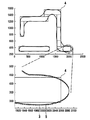
FIG. 6 shows the
図7は、別個の位置合わせ測定の結果が、この時点までに得られた結果に対して適用される、さらなるステップを示す。図において、特に図の下部に示される詳細な拡大において示されるのは、リソターゲット4であり、これはその真っ直ぐな境界と、空間像測定からフィッティングされた輪郭3(破線を用いて示される)と、別個に測定された位置合わせ誤差によってオフセットされた輪郭5とによって識別可能である。ここで、位置合わせ誤差は、特に、座標測定機を用いて確認されることができ、当然、位置合わせ誤差を確認するための他のプロセスも想定できる。得られる像は、その大きな情報の内容によって際立つ。第1にそれは、ウェハ上で期待されるようになる輪郭の現実的な表示(マスク検査システムの空間像から得られる)を含むが、第2に、それは各関心領域に対して期待されるようになる位置合わせ誤差も含む。特にウェハの同じ層上の構造体が、2つの異なるマスクによる二重露光を用いて生成されるためのものである場合、異なるが存在するマスクの位置合わせ誤差は、リソターゲットから外れたフィーチャの実際の輪郭と組み合わされて合計となり、結果として生じ得る欠陥を有して生成された構造体に繋がる。予見できる問題が、マスク測定に基づいた本発明による適時なやり方において特定され得る結果として、知られているシステムによって効果的で適切なマスク補正に取り組むことが可能である。
FIG. 7 shows a further step in which the results of the separate alignment measurements are applied to the results obtained so far. In the figure, especially in the detailed enlargement shown at the bottom of the figure, is the
しかし、上述の手法は、マスク検査システムによって記録された空間像と、位置合わせ測定システムによって記録された空間像とが、互いに異ならない、または互いにわずかしか異ならないことを仮定している。しかし、前述のシステムは、とりわけ照明および開口数の観点から著しく異なるので、この仮定はあまり正しくない。従って、位置合わせ測定システムによって確認された位置合わせ誤差は、マスク検査システムによって生成された空間像に対して、完全に移転可能ではない可能性がある。 However, the method described above assumes that the spatial image recorded by the mask inspection system and the spatial image recorded by the alignment measurement system are not or slightly different from each other. However, this assumption is not very correct, as the systems described above differ significantly, especially in terms of lighting and numerical aperture. Therefore, the alignment error confirmed by the alignment measurement system may not be completely transferable to the spatial image generated by the mask inspection system.
この問題を抑制するために、すでに知られている方法ステップに加えて、マスク設計から、シミュレーション、特にキルヒホッフまたは厳密なシミュレーションを用いて、位置合わせ像と、マスク検査システム像とが生成される。位置合わせ像のシミュレーションは位置合わせに対する値を供給し、特に、それは例えば歪みなどの知られている結像収差を考慮に入れる。このシミュレーションは通常、位置合わせを確認するためのいずれの場合にも実行される。2つのシミュレートされた像を互いに比較することから、位置合わせ測定システムと、マスク検査システムとの間の位置合わせ測定の差分誤差を導き出すことが可能であり、これはマスクのさらなる測定および認定の間に考慮に入れられ得る。 To suppress this problem, in addition to the already known method steps, the mask design produces an alignment image and a mask inspection system image using simulations, especially Kirchhoff's or rigorous simulations. The simulation of the alignment image provides a value for alignment, in particular it takes into account known imaging aberrations such as distortion. This simulation is typically performed in any case to confirm alignment. By comparing the two simulated images with each other, it is possible to derive the differential error of the alignment measurement between the alignment measurement system and the mask inspection system, which is the further measurement and certification of the mask. Can be taken into account in the meantime.
具体的には、x/y適合は、シミュレートされた空間像に基づいて初期に実行される(および、もはやリソターゲットに基づかない)。 Specifically, the x / y match is initially performed based on the simulated spatial image (and is no longer based on the litho target).
次いで、第2のステップにおいて、ならびにxおよびy値のいかなるさらなる適合なしに、閾値は、リソターゲットからそれぞれ考慮される構造体のCD値が、できるだけ最良の程度まで得られるように適合される。 Then, in the second step, and without any further adaptation of the x and y values, the thresholds are adjusted so that the CD value of each considered structure from the litho target is obtained to the best possible extent.
結果として、とりわけ、リソターゲットに関する確認された構造体のオフセットの表示が得られ、なぜならマスク設計のシミュレーションは、OPCの誤差を識別可能にするからである(すなわち、リソターゲットから始めてマスク設計がそれに基づいて定義されたソフトウェアの)。 The result is, among other things, a display of the confirmed structure offsets for the litho target, because the simulation of the mask design makes the OPC error identifiable (ie, starting with the litho target, the mask design makes it). Of software defined based on.
1 関心領域(ROI)
2 構造体
3 構造体端部
4 リソターゲット
5 位置合わせ測定からのオフセット輪郭
1 Area of interest (ROI)
2
Claims (7)
フォトマスクの少なくとも1つの領域の空間像を記録するステップと、
少なくとも1つの関心領域(1)を定義するステップと、
少なくとも1つの関心領域(1)内の構造体端部(3)を確認するステップと、
前記フォトマスクによって作り出されることになる所望の構造体(4)を提供するステップと、
前記確認された構造体端部(3)を前記所望の構造体(4)に適合させるステップと、
別個の位置合わせ測定の結果を用いて、前記適合された構造体端部を変位させるステップと
を含む方法。 A method for measuring photomasks for semiconductor lithography.
The step of recording a spatial image of at least one area of the photomask,
Steps to define at least one area of interest (1),
The step of confirming the structure end (3) in at least one region of interest (1), and
The step of providing the desired structure (4) that will be produced by the photomask, and
The step of adapting the confirmed structure end (3) to the desired structure (4),
A method comprising the step of displacing the fitted end of a structure using the results of separate alignment measurements.
請求項1に記載の方法。 After the step of recording the spatial image, there is a correction for the calculation of the image aberration of the system used to record the spatial image.
The method according to claim 1.
請求項1又は2に記載の方法。 In the step of fitting the identified structural end (3), a spatial image simulated based on the mask design is used.
The method according to claim 1 or 2.
請求項3に記載の方法。 The simulated spatial image is generated for an alignment measurement system and / or for a mask inspection system.
The method according to claim 3.
請求項1〜4のいずれか1項に記載の方法。 The identified information items are used to create a correction measure for the mask or for the scanner exposure process.
The method according to any one of claims 1 to 4.
請求項5に記載の方法。 One correction measure for the mask is a targeted physical stretch of the mask.
The method according to claim 5.
請求項5又は6に記載の方法。 A matching correction measure is created for at least two masks.
The method according to claim 5 or 6.
Priority Applications (1)
| Application Number | Priority Date | Filing Date | Title |
|---|---|---|---|
| JP2023097154A JP2023129405A (en) | 2020-02-18 | 2023-06-13 | Method for measuring photomasks |
Applications Claiming Priority (2)
| Application Number | Priority Date | Filing Date | Title |
|---|---|---|---|
| DE102020104167.5 | 2020-02-18 | ||
| DE102020104167.5A DE102020104167B4 (en) | 2020-02-18 | 2020-02-18 | Process for measuring photomasks |
Related Child Applications (1)
| Application Number | Title | Priority Date | Filing Date |
|---|---|---|---|
| JP2023097154A Division JP2023129405A (en) | 2020-02-18 | 2023-06-13 | Method for measuring photomasks |
Publications (1)
| Publication Number | Publication Date |
|---|---|
| JP2021144211A true JP2021144211A (en) | 2021-09-24 |
Family
ID=77060607
Family Applications (2)
| Application Number | Title | Priority Date | Filing Date |
|---|---|---|---|
| JP2021024113A Pending JP2021144211A (en) | 2020-02-18 | 2021-02-18 | Method for measuring photomasks |
| JP2023097154A Pending JP2023129405A (en) | 2020-02-18 | 2023-06-13 | Method for measuring photomasks |
Family Applications After (1)
| Application Number | Title | Priority Date | Filing Date |
|---|---|---|---|
| JP2023097154A Pending JP2023129405A (en) | 2020-02-18 | 2023-06-13 | Method for measuring photomasks |
Country Status (6)
| Country | Link |
|---|---|
| US (1) | US11899358B2 (en) |
| JP (2) | JP2021144211A (en) |
| KR (1) | KR102638175B1 (en) |
| CN (1) | CN113340564A (en) |
| DE (1) | DE102020104167B4 (en) |
| TW (1) | TWI788783B (en) |
Citations (7)
| Publication number | Priority date | Publication date | Assignee | Title |
|---|---|---|---|---|
| JP2009200499A (en) * | 2008-02-22 | 2009-09-03 | Interuniv Micro Electronica Centrum Vzw | Split and design guideline for double patterning |
| JP2009294308A (en) * | 2008-06-03 | 2009-12-17 | Nec Electronics Corp | Pattern verifying method, pattern verifying device, program and method of manufacturing semiconductor device |
| JP2010038944A (en) * | 2008-07-31 | 2010-02-18 | Toshiba Corp | Method of manufacturing photomask, and method of manufacturing semiconductor device using the photomask |
| JP2010199462A (en) * | 2009-02-27 | 2010-09-09 | Hitachi High-Technologies Corp | Pattern measuring device |
| JP2014082516A (en) * | 2009-12-29 | 2014-05-08 | Hitachi Ltd | Measuring method and device for pattern position and overlay |
| JP2015527740A (en) * | 2012-08-01 | 2015-09-17 | ケーエルエー−テンカー コーポレイション | Wafer inspection and / or prediction of one or more characteristics of devices formed on the wafer |
| JP2017058397A (en) * | 2015-09-14 | 2017-03-23 | 大日本印刷株式会社 | Method and system of evaluating transcription properties of photomask, and method of manufacturing photomask |
Family Cites Families (16)
| Publication number | Priority date | Publication date | Assignee | Title |
|---|---|---|---|---|
| US5504793A (en) * | 1995-02-17 | 1996-04-02 | Loral Federal Systems Company | Magnification correction for 1-X proximity X-Ray lithography |
| JP2005251983A (en) * | 2004-03-04 | 2005-09-15 | Renesas Technology Corp | Method and apparatus for charged particle beam mask inspection |
| KR100982135B1 (en) * | 2005-09-09 | 2010-09-14 | 에이에스엠엘 네델란즈 비.브이. | System and method for mask verification using an individual mask error model |
| KR100924335B1 (en) * | 2007-03-27 | 2009-11-02 | 주식회사 하이닉스반도체 | Method for correcting optical proximity using multi-dose simulation |
| KR100881194B1 (en) * | 2007-05-16 | 2009-02-05 | 삼성전자주식회사 | Method of inspecting mask using aerial image inspection equipment |
| KR100914297B1 (en) * | 2007-12-28 | 2009-08-27 | 주식회사 하이닉스반도체 | Method of OPC by using wafer pattern measure data |
| DE102008015631A1 (en) | 2008-03-20 | 2009-09-24 | Carl Zeiss Sms Gmbh | Method and device for measuring masks for photolithography |
| DE102009038558A1 (en) * | 2009-08-24 | 2011-03-10 | Carl Zeiss Sms Gmbh | Method for emulating a photolithographic process and mask inspection microscope for performing the method |
| WO2012013638A1 (en) | 2010-07-26 | 2012-02-02 | Carl Zeiss Sms Ltd. | Lithographic targets for uniformity control |
| TWI518446B (en) | 2011-12-19 | 2016-01-21 | 聯華電子股份有限公司 | Method for correcting layout pattern and method for manufacturing photomask |
| EP3037878B1 (en) | 2014-12-23 | 2020-09-09 | Aselta Nanographics | Method of applying vertex based corrections to a semiconductor design |
| US10176966B1 (en) | 2017-04-13 | 2019-01-08 | Fractilia, Llc | Edge detection system |
| CN107121893B (en) * | 2017-06-12 | 2018-05-25 | 中国科学院上海光学精密机械研究所 | Photoetching projection objective lens thermal aberration on-line prediction method |
| DE102017115365B4 (en) * | 2017-07-10 | 2020-10-15 | Carl Zeiss Smt Gmbh | Semiconductor lithography mask inspection device and process |
| DE102018111972A1 (en) | 2018-05-18 | 2019-05-29 | Carl Zeiss Smt Gmbh | Method for determining registration errors on a photomask for semiconductor lithography |
| DE102018210315B4 (en) * | 2018-06-25 | 2021-03-18 | Carl Zeiss Smt Gmbh | Method for detecting a structure of a lithography mask and device for carrying out the method |
-
2020
- 2020-02-18 DE DE102020104167.5A patent/DE102020104167B4/en active Active
-
2021
- 2021-02-17 US US17/177,411 patent/US11899358B2/en active Active
- 2021-02-18 JP JP2021024113A patent/JP2021144211A/en active Pending
- 2021-02-18 CN CN202110190657.9A patent/CN113340564A/en active Pending
- 2021-02-18 TW TW110105486A patent/TWI788783B/en active
- 2021-02-18 KR KR1020210021797A patent/KR102638175B1/en active IP Right Grant
-
2023
- 2023-06-13 JP JP2023097154A patent/JP2023129405A/en active Pending
Patent Citations (7)
| Publication number | Priority date | Publication date | Assignee | Title |
|---|---|---|---|---|
| JP2009200499A (en) * | 2008-02-22 | 2009-09-03 | Interuniv Micro Electronica Centrum Vzw | Split and design guideline for double patterning |
| JP2009294308A (en) * | 2008-06-03 | 2009-12-17 | Nec Electronics Corp | Pattern verifying method, pattern verifying device, program and method of manufacturing semiconductor device |
| JP2010038944A (en) * | 2008-07-31 | 2010-02-18 | Toshiba Corp | Method of manufacturing photomask, and method of manufacturing semiconductor device using the photomask |
| JP2010199462A (en) * | 2009-02-27 | 2010-09-09 | Hitachi High-Technologies Corp | Pattern measuring device |
| JP2014082516A (en) * | 2009-12-29 | 2014-05-08 | Hitachi Ltd | Measuring method and device for pattern position and overlay |
| JP2015527740A (en) * | 2012-08-01 | 2015-09-17 | ケーエルエー−テンカー コーポレイション | Wafer inspection and / or prediction of one or more characteristics of devices formed on the wafer |
| JP2017058397A (en) * | 2015-09-14 | 2017-03-23 | 大日本印刷株式会社 | Method and system of evaluating transcription properties of photomask, and method of manufacturing photomask |
Also Published As
| Publication number | Publication date |
|---|---|
| US20210255541A1 (en) | 2021-08-19 |
| KR20210105838A (en) | 2021-08-27 |
| DE102020104167A1 (en) | 2021-08-19 |
| DE102020104167B4 (en) | 2023-01-26 |
| CN113340564A (en) | 2021-09-03 |
| US11899358B2 (en) | 2024-02-13 |
| JP2023129405A (en) | 2023-09-14 |
| KR102638175B1 (en) | 2024-02-19 |
| TW202136901A (en) | 2021-10-01 |
| TWI788783B (en) | 2023-01-01 |
Similar Documents
| Publication | Publication Date | Title |
|---|---|---|
| KR101991762B1 (en) | Method of measuring a property of a target structure, inspection apparatus, lithographic system and device manufacturing method | |
| US8913120B2 (en) | Method for emulation of a photolithographic process and mask inspection microscope for performing the method | |
| JP4911541B2 (en) | Method for in-situ measurement of aberrations in an optical imaging system of a lithography tool | |
| US10712672B2 (en) | Method of predicting patterning defects caused by overlay error | |
| KR20070062427A (en) | Method and apparatus for evaluating photomask, and method for manufacturing semiconductor device | |
| TW201732450A (en) | Improvements in gauge pattern selection | |
| KR102451533B1 (en) | Verification method of mask for microlithography | |
| CN112561873B (en) | CDSEM image virtual measurement method based on machine learning | |
| US9785058B2 (en) | Method for ascertaining distortion properties of an optical system in a measurement system for microlithography | |
| CN101320219B (en) | Field measurement method for optical aberration of imaging optical system | |
| KR102326191B1 (en) | Device manufacturing process | |
| JP2008242112A (en) | Mask pattern evaluation device and manufacturing method of photomask | |
| US20190384164A1 (en) | Method of determining pellicle degradation compensation corrections, and associated lithographic apparatus and computer program | |
| US20190391500A1 (en) | Method of measuring variation, inspection system, computer program, and computer system | |
| JP7339826B2 (en) | Mark positioning method, lithographic method, article manufacturing method, program and lithographic apparatus | |
| JP2021144211A (en) | Method for measuring photomasks | |
| JP6440498B2 (en) | Lithographic system, lithographic method, and article manufacturing method | |
| JP2019204058A5 (en) | ||
| JP2022176170A (en) | Method for Determining Registration Error | |
| JP7390104B2 (en) | Microlithographic masks, methods for determining image edge positions of structures of such masks, and systems for implementing such methods | |
| KR102663061B1 (en) | Microlithographic mask, method for determining edge positions of the images of the structures of such a mask and system for carrying out such a method | |
| JP2004356553A (en) | Superposition inspection method and superposition inspection device | |
| KR20230075369A (en) | Mask inspection for semiconductor specimen fabrication |
Legal Events
| Date | Code | Title | Description |
|---|---|---|---|
| A621 | Written request for application examination |
Free format text: JAPANESE INTERMEDIATE CODE: A621 Effective date: 20210617 |
|
| A131 | Notification of reasons for refusal |
Free format text: JAPANESE INTERMEDIATE CODE: A131 Effective date: 20220609 |
|
| A601 | Written request for extension of time |
Free format text: JAPANESE INTERMEDIATE CODE: A601 Effective date: 20220909 |
|
| A521 | Request for written amendment filed |
Free format text: JAPANESE INTERMEDIATE CODE: A523 Effective date: 20221108 |
|
| A02 | Decision of refusal |
Free format text: JAPANESE INTERMEDIATE CODE: A02 Effective date: 20230213 |