JP2021136816A - Charge/discharge control device and electronic apparatus - Google Patents
Charge/discharge control device and electronic apparatus Download PDFInfo
- Publication number
- JP2021136816A JP2021136816A JP2020033142A JP2020033142A JP2021136816A JP 2021136816 A JP2021136816 A JP 2021136816A JP 2020033142 A JP2020033142 A JP 2020033142A JP 2020033142 A JP2020033142 A JP 2020033142A JP 2021136816 A JP2021136816 A JP 2021136816A
- Authority
- JP
- Japan
- Prior art keywords
- circuit
- power
- power supply
- charge
- voltage
- Prior art date
- Legal status (The legal status is an assumption and is not a legal conclusion. Google has not performed a legal analysis and makes no representation as to the accuracy of the status listed.)
- Pending
Links
Images


Classifications
-
- H—ELECTRICITY
- H02—GENERATION; CONVERSION OR DISTRIBUTION OF ELECTRIC POWER
- H02J—ELECTRIC POWER NETWORKS; CIRCUIT ARRANGEMENTS OR SYSTEMS FOR SUPPLYING OR DISTRIBUTING ELECTRIC POWER; SYSTEMS FOR STORING ELECTRIC ENERGY
- H02J7/00—Circuit arrangements for charging or discharging batteries or for supplying loads from batteries
- H02J7/865—Battery or charger load switching, e.g. concurrent charging and load supply
-
- H—ELECTRICITY
- H02—GENERATION; CONVERSION OR DISTRIBUTION OF ELECTRIC POWER
- H02J—ELECTRIC POWER NETWORKS; CIRCUIT ARRANGEMENTS OR SYSTEMS FOR SUPPLYING OR DISTRIBUTING ELECTRIC POWER; SYSTEMS FOR STORING ELECTRIC ENERGY
- H02J7/00—Circuit arrangements for charging or discharging batteries or for supplying loads from batteries
- H02J7/90—Regulation of charging or discharging current or voltage
- H02J7/933—Regulation of charging or discharging current or voltage the cycle being controlled or terminated in response to electric parameters
-
- H—ELECTRICITY
- H02—GENERATION; CONVERSION OR DISTRIBUTION OF ELECTRIC POWER
- H02J—ELECTRIC POWER NETWORKS; CIRCUIT ARRANGEMENTS OR SYSTEMS FOR SUPPLYING OR DISTRIBUTING ELECTRIC POWER; SYSTEMS FOR STORING ELECTRIC ENERGY
- H02J7/00—Circuit arrangements for charging or discharging batteries or for supplying loads from batteries
- H02J7/855—Circuit arrangements for charging or discharging batteries or for supplying loads from batteries with circuits adapted for supplying loads from the battery
-
- H—ELECTRICITY
- H02—GENERATION; CONVERSION OR DISTRIBUTION OF ELECTRIC POWER
- H02J—ELECTRIC POWER NETWORKS; CIRCUIT ARRANGEMENTS OR SYSTEMS FOR SUPPLYING OR DISTRIBUTING ELECTRIC POWER; SYSTEMS FOR STORING ELECTRIC ENERGY
- H02J7/00—Circuit arrangements for charging or discharging batteries or for supplying loads from batteries
- H02J7/90—Regulation of charging or discharging current or voltage
-
- H—ELECTRICITY
- H04—ELECTRIC COMMUNICATION TECHNIQUE
- H04R—LOUDSPEAKERS, MICROPHONES, GRAMOPHONE PICK-UPS OR LIKE ACOUSTIC ELECTROMECHANICAL TRANSDUCERS; ELECTRIC HEARING AIDS; PUBLIC ADDRESS SYSTEMS
- H04R1/00—Details of transducers, loudspeakers or microphones
- H04R1/10—Earpieces; Attachments therefor ; Earphones; Monophonic headphones
- H04R1/1025—Accumulators specially adapted for earpieces; Arrangements specially adapted for charging thereof
-
- H—ELECTRICITY
- H04—ELECTRIC COMMUNICATION TECHNIQUE
- H04R—LOUDSPEAKERS, MICROPHONES, GRAMOPHONE PICK-UPS OR LIKE ACOUSTIC ELECTROMECHANICAL TRANSDUCERS; ELECTRIC HEARING AIDS; PUBLIC ADDRESS SYSTEMS
- H04R25/00—Electric hearing aids
- H04R25/30—Monitoring or testing of hearing aids, e.g. functioning, settings, battery power
- H04R25/305—Self-monitoring or self-testing
-
- H—ELECTRICITY
- H02—GENERATION; CONVERSION OR DISTRIBUTION OF ELECTRIC POWER
- H02J—ELECTRIC POWER NETWORKS; CIRCUIT ARRANGEMENTS OR SYSTEMS FOR SUPPLYING OR DISTRIBUTING ELECTRIC POWER; SYSTEMS FOR STORING ELECTRIC ENERGY
- H02J2207/00—Details of circuit arrangements for charging or discharging batteries or supplying loads from batteries
- H02J2207/20—Charging or discharging characterised by the power electronics converter
-
- H—ELECTRICITY
- H04—ELECTRIC COMMUNICATION TECHNIQUE
- H04R—LOUDSPEAKERS, MICROPHONES, GRAMOPHONE PICK-UPS OR LIKE ACOUSTIC ELECTROMECHANICAL TRANSDUCERS; ELECTRIC HEARING AIDS; PUBLIC ADDRESS SYSTEMS
- H04R1/00—Details of transducers, loudspeakers or microphones
- H04R1/10—Earpieces; Attachments therefor ; Earphones; Monophonic headphones
- H04R1/1016—Earpieces of the intra-aural type
-
- H—ELECTRICITY
- H04—ELECTRIC COMMUNICATION TECHNIQUE
- H04R—LOUDSPEAKERS, MICROPHONES, GRAMOPHONE PICK-UPS OR LIKE ACOUSTIC ELECTROMECHANICAL TRANSDUCERS; ELECTRIC HEARING AIDS; PUBLIC ADDRESS SYSTEMS
- H04R2225/00—Details of deaf aids covered by H04R25/00, not provided for in any of its subgroups
- H04R2225/31—Aspects of the use of accumulators in hearing aids, e.g. rechargeable batteries or fuel cells
-
- Y—GENERAL TAGGING OF NEW TECHNOLOGICAL DEVELOPMENTS; GENERAL TAGGING OF CROSS-SECTIONAL TECHNOLOGIES SPANNING OVER SEVERAL SECTIONS OF THE IPC; TECHNICAL SUBJECTS COVERED BY FORMER USPC CROSS-REFERENCE ART COLLECTIONS [XRACs] AND DIGESTS
- Y02—TECHNOLOGIES OR APPLICATIONS FOR MITIGATION OR ADAPTATION AGAINST CLIMATE CHANGE
- Y02E—REDUCTION OF GREENHOUSE GAS [GHG] EMISSIONS, RELATED TO ENERGY GENERATION, TRANSMISSION OR DISTRIBUTION
- Y02E60/00—Enabling technologies; Technologies with a potential or indirect contribution to GHG emissions mitigation
- Y02E60/10—Energy storage using batteries
Landscapes
- Engineering & Computer Science (AREA)
- Power Engineering (AREA)
- Physics & Mathematics (AREA)
- Acoustics & Sound (AREA)
- Signal Processing (AREA)
- Health & Medical Sciences (AREA)
- General Health & Medical Sciences (AREA)
- Otolaryngology (AREA)
- Neurosurgery (AREA)
- Charge And Discharge Circuits For Batteries Or The Like (AREA)
- Power Sources (AREA)
- Secondary Cells (AREA)
Abstract
Description
本発明は、充放電制御装置および電子機器に関するものである。 The present invention relates to a charge / discharge control device and an electronic device.
特許文献1には、USB電源を利用するUSBファン装置であって、ファンを駆動するモータと、モータを駆動するファン駆動回路と、USB電源に非接続のときにモータに電力を供給する充電池と、ファン駆動回路への電力の出力制御を行うマイコンと、USB電源からの電流を充電池へ出力制御する充電系制御回路と、電源切替回路と、を備える。 Patent Document 1 describes a USB fan device that uses a USB power supply, that is, a motor that drives the fan, a fan drive circuit that drives the motor, and a rechargeable battery that supplies power to the motor when not connected to the USB power supply. It also includes a microcomputer that controls the output of electric power to the fan drive circuit, a charging system control circuit that controls the output of the current from the USB power supply to the rechargeable battery, and a power supply switching circuit.
このうち、電源切替回路は、USB電源と充電池から供給される電流を択一的に切り替えてマイコンまたは充電系制御回路へ振り分けて出力する。 Of these, the power supply switching circuit selectively switches the current supplied from the USB power supply and the rechargeable battery, distributes the current to the microcomputer or the charging system control circuit, and outputs the current.
このようなUSBファン装置では、電源として、USB電源または充電池のどちらを使用するか、選ぶことができるので、利便性が高い。 In such a USB fan device, it is highly convenient because it is possible to select whether to use a USB power source or a rechargeable battery as the power source.
特許文献1に記載のUSBファン装置では、充電池が過放電状態にある場合、USB電源を接続したとしても、電源切替回路が動作せず、電源の切り替えが行われないおそれがある。この場合、マイコンや充電系制御回路に通電させることができず、USBファン装置が起動しない。 In the USB fan device described in Patent Document 1, when the rechargeable battery is in an over-discharged state, the power supply switching circuit may not operate and the power supply may not be switched even if the USB power supply is connected. In this case, the microcomputer and the charging system control circuit cannot be energized, and the USB fan device does not start.
本発明の適用例に係る充放電制御装置は、
受電電力に基づいて、給電対象に電力を供給する第1の電源回路と、
受電電力に基づいて、充電対象を充電する充電回路と、
前記充電対象から出力された放電電力に基づいて、前記給電対象に電力を供給する第2の電源回路と、
前記第1の電源回路および前記第2の電源回路の動作を制御する制御部と、
を備え、
前記充電対象の電圧が所定値未満である場合に、前記制御部は、前記第1の電源回路により、前記給電対象に電力を供給させることを特徴とする。
The charge / discharge control device according to the application example of the present invention is
A first power supply circuit that supplies power to the power supply target based on the received power,
A charging circuit that charges the charging target based on the received power,
A second power supply circuit that supplies power to the power supply target based on the discharge power output from the charging target, and
A control unit that controls the operation of the first power supply circuit and the second power supply circuit,
With
When the voltage of the charging target is less than a predetermined value, the control unit is characterized in that the power supply target is supplied with electric power by the first power supply circuit.
本発明の適用例に係る電子機器は、
本発明の適用例に係る充放電制御装置を備えることを特徴とする。
The electronic device according to the application example of the present invention is
It is characterized by including a charge / discharge control device according to an application example of the present invention.
以下、本発明の充放電制御装置および電子機器の好適な実施形態を添付図面に基づいて詳細に説明する。
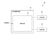
1.電子機器
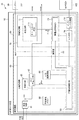
図1は、実施形態に係る電子機器の構成を示すブロック図である。図2は、図1に示す電子機器の詳細な構成を示すブロック図である。
Hereinafter, preferred embodiments of the charge / discharge control device and the electronic device of the present invention will be described in detail with reference to the accompanying drawings.
1. 1. Electronic device FIG. 1 is a block diagram showing a configuration of an electronic device according to an embodiment. FIG. 2 is a block diagram showing a detailed configuration of the electronic device shown in FIG.
図1に示す電子機器30は、制御回路50を含む充放電制御装置10と、給電対象99と、充電対象92と、を備える。
The
給電対象99は、制御回路50が給電を行う対象となるデバイスであり、例えば図2に示す処理回路100である。
The
充電対象92は、制御回路50が充電を行う対象となるデバイスであり、例えば図2に示すバッテリー90である。
The
制御回路50は、受電電力に基づいて充電対象92の定電流充電または定電圧充電等を行うとともに、受電電力または充電対象92からの放電電力に基づいて給電対象99に電力を供給する。
The
制御回路50は、有線である電源線を介した有接点の電力伝送により電力を受電する構成を有していてもよいし、無接点の電力伝送により電力を受電する構成を有していてもよい。
The
処理回路100は、制御回路50の動作を制御する。具体的には、処理回路100は、制御回路50を制御するための各種の制御処理を実行する。処理回路100は、例えば、制御回路50に対してコマンドを発行したり、制御回路50に対して各種の情報を設定することで、制御回路50の動作を制御したりする。このような処理回路100は、例えば、DSP(Digital Signal Processor)、CPU(Central Processing Unit)、ASIC、マイクロコントローラー等のプロセッサーにより実現される。また、処理回路100は、音声処理や画像処理等の各種デジタル信号処理を実行するものであってもよい。
The
バッテリー90は、例えば充電可能な二次電池である。この二次電池としては、例えば、リチウムイオン二次電池、リチウムイオンポリマー二次電池のようなリチウム二次電池、ニッケル−水素二次電池、ニッケル−カドミウム二次電池のようなニッケル二次電池等が挙げられる。
The
2.第1実施形態に係る充放電制御装置
2.1.充放電制御装置の構成
図2に示す充放電制御装置10が含む制御回路50は、充電系回路60と、放電系回路70と、を備える。
2. Charge / discharge control device according to the first embodiment 2.1. Configuration of Charge / Discharge Control Device The
このうち、充電系回路60は、受電回路61と、充電回路65と、リニアレギュレーター62と、充電系制御回路63と、A/D変換回路66と、不揮発性メモリー68と、を備える。また、放電系回路70は、給電回路71と、放電系制御回路73と、インターフェース回路74と、レジスター76と、を備える。以下、充電系回路60および放電系回路70の各部について詳述する。
Of these, the
図2に示す充電系回路60は、バッテリー90の充電を行うとともに、必要に応じて、処理回路100に給電を行う回路である。具体的には、充電系回路60は、受電電力に基づいて動作し、バッテリー90の充電を行う。また、それとともに、充電系回路60は、処理回路100に所定の電圧で電力を供給する。
The
充電系回路60は、例えば、バッテリー90を定電流充電するための制御、バッテリー90を定電圧充電するための制御等を行う。具体的には、充電系回路60は、まず、バッテリー90の定電流充電を行い、その後、バッテリー90の充電電圧が所定電圧に達した場合、定電流充電から定電圧充電に切り替える。
The
定電流充電は、電流が一定となる定電流の充電電流でバッテリー90を充電するものであり、定電圧充電は、電圧が一定となる定電圧の充電電圧でバッテリー90を充電するものである。定電流充電を行うことで、充電対象の充電電圧を短時間で上昇させることができる。定電圧充電を行うことで、充電電流は徐々に減少するため、充電電流の急激な変動を抑制し、充電の電流値や電圧値の安定化等が図られる。なお、定電流充電における充電電流は、完全に一定である必要はなく、略一定であればよく、定電圧充電における充電電圧も、完全に一定である必要はなく、略一定であればよい。
Constant current charging charges the
受電回路61は、例えば交流の外部電圧を直流の整流電圧VCCに変換して出力する。
充電回路65は、整流電圧VCCを受電し、この整流電圧VCCに基づいて動作するとともに、バッテリー90の充電を行う機能を有する。具体的には、充電回路65は、整流電圧VCCに基づいて定電流充電または定電圧充電でバッテリー90を充電する。
The power receiving
The
リニアレギュレーター62は、整流電圧VCCを受電し、この整流電圧VCCに基づいて動作するとともに、処理回路100に電力を供給する機能を有する。具体的には、リニアレギュレーター62は、整流電圧VCCを降圧し、所定の出力電圧VOUT1を生成して、処理回路100に供給する。リニアレギュレーター62は、例えば、LDO(Low Dropout)レギュレーター等のアナログレギュレーターにより実現される。
The
充電系制御回路63は、充電回路65の動作を制御し、バッテリー90の充電を行わせるとともに、リニアレギュレーター62の動作を制御し、処理回路100へ電力を供給させる。また、充電系制御回路63は、インターフェース回路74およびレジスター76の動作も制御する。例えば、充電系制御回路63は、インターフェース回路74のインターフェース処理を制御したり、レジスター76への情報の書き込みや読み出しを制御したりする。具体的には、充電系制御回路63は、レジスター76からの情報を読み出して、充電回路65の動作を制御する。
The charging
A/D変換回路66は、例えば、バッテリー90のバッテリー電圧VBATをA/D変換し、その変換値を充電系制御回路63等に出力する。
The A /
不揮発性メモリー68は、例えばデータの電気的な消去が可能なEEPROM(Electrically Erasable Programmable Read-Only Memory)や、FAMOS(Floating gate Avalanche injection MOS)等を用いたOTP(One Time Programmable)のメモリー等により実現される。なお、図2では、不揮発性メモリー68が制御回路50に設けられているが、制御回路50の外部に設けられていてもよい。
The
図2に示す放電系回路70は、バッテリー90の放電動作を行って、放電電力を処理回路100に供給する回路である。具体的には、放電系回路70は、バッテリー90のバッテリー電圧VBATに基づいて動作し、出力電圧VOUT2を、処理回路100に供給する。これにより、処理回路100は、出力電圧VOUT2に基づいて動作する。
The
給電回路71は、バッテリー電圧VBATに基づく出力電圧VOUT2を、処理回路100に供給する。図2に示す給電回路71は、チャージポンプ回路711を含む。チャージポンプ回路711は、バッテリー電圧VBATを降圧するチャージポンプ動作を行い、出力電圧VOUT2を生成する。そして、生成した出力電圧VOUT2を処理回路100に供給する。
The
チャージポンプ回路711は、例えばDC−DCコンバーター、具体的にはスイッチングレギュレーターにより実現される。なお、チャージポンプ回路711に代えて、リニアレギュレーター、例えばアナログレギュレーターを用いるようにしてもよい。
The
放電系制御回路73は、給電回路71の動作を制御し、バッテリー電圧VBATに基づく出力電圧VOUT2の生成、出力を行わせる。また、放電系制御回路73は、インターフェース回路74およびレジスター76の動作も制御する。例えば、放電系制御回路73は、インターフェース回路74のインターフェース処理を制御したり、レジスター76への情報の書き込みや読み出しを制御したりする。
The discharge
なお、前述した充電系制御回路63および放電系制御回路73により、制御部80が構成されている。つまり、制御部80は、受電回路61からの電力で動作し、充電回路65やリニアレギュレーター62の動作を制御する回路(充電系制御回路63等)と、バッテリー90からの電力で動作し、チャージポンプ回路711を含む給電回路71の動作を制御する回路(放電系制御回路73等)と、を含む。
The
インターフェース回路74は、処理回路100とのインターフェース処理を行う回路である。インターフェース回路74は、例えば、処理回路100が発行したコマンドを受け付けたり、処理回路100が設定した情報を受け付けたりするインターフェース処理を行う。インターフェース回路74は、例えば、SPI(Serial Peripheral Interface)、I2C(Inter-Integrated Circuit)等のシリアルインターフェース回路により実現される。また、インターフェース回路74は、例えば、差動信号を用いたシリアルインターフェース回路、パラレルインタフェース回路等であってもよい。
The
レジスター76には、インターフェース回路74を介して処理回路100により各種の情報が書き込まれる。また、レジスター76に書き込まれた各種の情報は、インターフェース回路74を介して処理回路100により読み出される。
Various information is written to the
レジスター76は、例えば、フリップフロップ回路、RAM(Random Access Memory)のようなメモリー等により実現される。
The
各種の情報としては、例えば、処理回路100からのコマンド、電流設定の情報等が挙げられる。
Examples of various types of information include commands from the
インターフェース回路74およびレジスター76は、それぞれ、バッテリー90から出力されたバッテリー電圧VBAT、または、リニアレギュレーター62から出力された出力電圧VOUT1、のいずれかに基づいて動作する。したがって、インターフェース回路74およびレジスター76は、整流電圧VCCを受電している状態、または、整流電圧VCCを受電していなくてもバッテリー90が放電可能な状態、のいずれかであれば、動作することができる。これにより、これらの状態であれば、処理回路100は、インターフェース回路74を介してレジスター76に情報を書き込んだり、記憶させておいた情報を読み出したりすることができる。また、レジスター76は、記憶した情報を保持し、例えば充電系制御回路63による情報の読み出しを可能にする。
The
制御回路50では、処理回路100からの電流設定を受け付ける。例えば、処理回路100が、定電流充電の電流設定のためのコマンドを発行したり、定電流充電の電流設定のための情報を設定したりしたときに、これらのコマンドや情報の設定を受け付ける。そして、制御回路50は、処理回路100による電流設定に基づいて、定電流充電を行う。具体的には、制御回路50は、電流モードに対応する電流値を充電電流として、バッテリー90を充電する定電流充電を行う。また、電流設定が、電流値である場合、制御回路50は、設定された電流値を充電電流として、バッテリー90を充電する定電流充電を行う。
The
また、不揮発性メモリー68は、電流モードに対応する電流値を記憶する。例えば、電流設定として、第1電流値で定電流充電を行う第1電流モードと、第1電流値とは異なる第2電流値で定電流充電を行う第2電流モードと、がある場合、不揮発性メモリー68は、第1電流値および第2電流値を記憶する。そして、処理回路100により、第1電流モードを設定するコマンドが発行された場合、充電系制御回路63は、レジスター76に記憶されている電流設定を読み出し、それに基づいて、不揮発性メモリー68に記憶されている第1電流値を読み出す。これにより、充電系制御回路63は、第1電流値で定電流充電を行うように充電回路65の動作を制御する。また、処理回路100により、第2電流モードを設定するコマンドが発行された場合、充電系制御回路63は、レジスター76に記憶されている電流設定を読み出し、それに基づいて、不揮発性メモリー68に記憶されている第2電流値を読み出す。これにより、充電系制御回路63は、第2電流値で定電流充電を行うように充電回路65の動作を制御する。
Further, the
このようにして、電流値が異なる複数の電流モードを使い分けながらバッテリー90を充電することにより、バッテリー90の周囲の環境やバッテリー90のスペック、種類等に応じて、充電時間を短縮したり、バッテリー90の劣化を抑制したりすることができる。その結果、バッテリー90の状態に応じた最適な充電が可能になる。
In this way, by charging the
なお、充電系制御回路63は、定電流充電の充電電流を自律的に制御してもよい。つまり、充電系制御回路63は、バッテリー電圧VBATのA/D変換値に基づいて自律的に充電回路65の動作を制御するように構成されていてもよい。
The charging
以上のような制御回路50では、充電系制御回路63の動作により、処理回路100への電力の供給元を、リニアレギュレーター62とチャージポンプ回路711との間で切り替える。具体的には、充電回路65が整流電圧VCCを受電しているとき、充電系制御回路63は、バッテリー電圧VBATに応じて、処理回路100への電力の供給元を、出力電圧VOUT1を出力するリニアレギュレーター62と、出力電圧VOUT2を出力するチャージポンプ回路711と、の間で切り替える。つまり、充電回路65が整流電圧VCCを受電しているときには、バッテリー電圧VBATの電圧値に応じて、整流電圧VCCを降圧した出力電圧VOUT1を処理回路100に供給することができるように、制御回路50が構成されている。
In the
これにより、制御回路50は、バッテリー90が過放電状態にあるときでも、処理回路100への電力の供給が可能になる。その結果、バッテリー90の充電状態によらず、処理回路100による各種処理を実行させることができる。
As a result, the
なお、制御回路50は、充電回路65が整流電圧VCCを受電したときには、バッテリー90の状態にかかわらず、リニアレギュレーター62から出力された出力電圧VOUT1を、処理回路100に供給するように動作してもよい。この場合、スイッチングレギュレーターに比べてノイズを発生させにくいというリニアレギュレーター62の利点を活かし、出力電圧VOUT1に混入するノイズを抑制し、ノイズに起因した処理回路100の誤動作を抑制することができる。
When the charging
以上のような充放電制御装置10としては、例えば、ASIC(Application Specific Integrated Circuit)のような半導体のICチップが挙げられる。ICチップは、例えばパッケージに実装される回路装置である。また、処理回路100を実現する回路装置は、充放電制御装置10のICチップとは別のICチップとされるが、制御回路50を実現する充放電制御装置10と、処理回路100を実現する回路装置とが、1つのICチップであってもよいし、1つのパッケージに実装されていてもよい。また、充放電制御装置10も、複数の回路装置が配線基板等を介して接続されてなる構造を有していてもよい。例えば、制御回路50が備える要素のうち、不揮発性メモリー68およびレジスター76等は、充電回路65や給電回路71を含むICチップの外部に設けられていてもよい。
Examples of the charge /
2.2.充放電制御装置の動作例
図3は、充放電制御装置10の動作例を説明するフローチャートである。
2.2. Operation Example of Charge / Discharge Control Device FIG. 3 is a flowchart illustrating an operation example of the charge /
制御回路50では、充電回路65が整流電圧VCCを受電しているとき、つまり、充放電制御装置10が外部電圧(受電電力)を受電しているとき、ステップS1として、まず、開放状態のバッテリー90のバッテリー電圧VBATを測定する。具体的には、A/D変換回路66がバッテリー電圧VBATのA/D変換(アナログ/デジタル変換)を行う。
In the
図2に示す制御部80の充電系制御回路63は、ステップS2として、バッテリー電圧VBATのA/D変換値と、所定のしきい値電圧VBFと、の比較を行う。そして、バッテリー電圧VBATがしきい値電圧VBFよりも低い場合には、充電系制御回路63は、バッテリー90が過放電状態にあると判断する。一方、バッテリー電圧VBATがしきい値電圧VBF以上である場合には、充電系制御回路63は、バッテリー90が十分に充電され、放電可能な状態にあると判断する。
In step S2, the charging
所定のしきい値電圧VBFは、例えば、不揮発性メモリー68に記憶させておくことができる。また、しきい値電圧VBFは、例えば、バッテリー90が安定して放電可能な状態にあるときのバッテリー電圧VBATの下限値である。
The predetermined threshold voltage VBF can be stored in, for example, the
そして、充電系制御回路63は、バッテリー電圧VBATがしきい値電圧VBF未満、つまり、バッテリー90が過放電状態にあると判断した場合、ステップS3として、リニアレギュレーター62の動作を制御する制御信号ENorをアクティブにする。これにより、リニアレギュレーター62は、出力電圧VOUT1を処理回路100に供給する。出力電圧VOUT1は、整流電圧VCCが降圧された電圧である。
Then, when the charging
また、この場合、図2に示す制御部80の放電系制御回路73は、チャージポンプ回路711の動作を制御する制御信号ENchを非アクティブにする。これにより、チャージポンプ回路711は、バッテリー電圧VBAT/3(出力電圧VOUT2)を出力しない。
ステップS3の終了後、ステップS1に戻る。
Further, in this case, the discharge
After the end of step S3, the process returns to step S1.
ステップS1では、再び、開放状態のバッテリー90のバッテリー電圧VBATを測定する。そして、ステップS2では、再び、バッテリー電圧VBATとしきい値電圧VBFとの比較を行う。このとき、バッテリー90の充電が十分に進んでいた場合には、バッテリー電圧VBATがしきい値電圧VBF以上となる。
In step S1, the battery voltage VBAT of the
この場合、放電系制御回路73は、バッテリー90が放電可能な状態にあると判断し、ステップS4として、チャージポンプ回路711の動作を制御する制御信号ENchをアクティブにする。これにより、給電回路71は、バッテリー電圧VBAT/3を出力電圧VOUT2として処理回路100に供給する。バッテリー電圧VBAT/3は、チャージポンプ回路711のチャージポンプ動作により、バッテリー電圧VBATが約3分の1に降圧された電圧である。なお、この降圧比は、特に限定されない。
In this case, the discharge
また、この場合、充電系制御回路63は、リニアレギュレーター62の動作を制御する制御信号ENorを非アクティブにする。これにより、リニアレギュレーター62は、出力電圧VOUT1を出力しない。
Further, in this case, the charging
以上のような動作例によれば、バッテリー90が過放電状態にあるときでも、処理回路100への電力の供給が可能になる。その結果、バッテリー90の充電状態によらず、処理回路100による各種処理を実行させることができる。
According to the above operation example, it is possible to supply electric power to the
なお、上記動作例は、一例であり、バッテリー90が放電可能な状態に至っても、制御回路50は、引き続き、リニアレギュレーター62の出力電圧VOUT1を処理回路100に供給するように動作してもよい。
The above operation example is an example, and even when the
以上のように、本実施形態に係る充放電制御装置10は、受電電力に基づいて、処理回路100(給電対象99)に電力を供給するリニアレギュレーター62(第1の電源回路)と、受電電力に基づいて、バッテリー90(充電対象92)を充電する充電回路65と、バッテリー90から出力された放電電力であるバッテリー電圧VBATに基づいて、処理回路100に電力を供給するチャージポンプ回路711(第2の電源回路)と、リニアレギュレーター62およびチャージポンプ回路711の動作を制御する制御部80と、を備える。そして、バッテリー90のバッテリー電圧VBATが所定のしきい値電圧VBF(所定値)未満である場合に、制御部80は、リニアレギュレーター62により、処理回路100に電力を供給させる。
As described above, the charge /
このような構成によれば、充放電制御装置10は、整流電圧VCCの受電時、バッテリー90の状態によらず、処理回路100に電力を供給することができる。このため、例えば、バッテリー90が過放電状態にあるときでも、処理回路100への電力の供給が可能になり、処理回路100による各種処理を実行させることができる。
According to such a configuration, the charge /
また、バッテリー90(充電対象92)のバッテリー電圧VBATがしきい値電圧VBF(所定値)以上である場合に、制御部80は、チャージポンプ回路711(第2の電源回路)により、処理回路100(給電対象99)に電力を供給させることが好ましい。
Further, when the battery voltage VBAT of the battery 90 (charge target 92) is equal to or higher than the threshold voltage VBF (predetermined value), the
チャージポンプ回路711は、例えば、スイッチングレギュレーターのようなDC−DCコンバーターで構成されるため、リニアレギュレーター62に比べて、消費電力が小さい。このため、バッテリー90が放電可能な状態になった時点で、チャージポンプ回路711から給電させることにより、電子機器30の低消費電力化を図ることができる。
Since the
また、前述したように、チャージポンプ回路711(第2の電源回路)は、リニアレギュレーター62(第1の電源回路)よりも電力変換効率が高い回路であるのが好ましい。これにより、整流電圧VCCを受電しているときでも、チャージポンプ回路711から給電させることにより、電子機器30の低消費電力化を図ることができる。
Further, as described above, the charge pump circuit 711 (second power supply circuit) is preferably a circuit having higher power conversion efficiency than the linear regulator 62 (first power supply circuit). As a result, even when the rectified voltage VCS is being received, the power consumption of the
また、前述したように、バッテリー90(充電対象92)のバッテリー電圧VBATが、所定のしきい値電圧VBF(所定値)未満からしきい値電圧VBF(所定値)以上に変化した場合に、制御部80は、処理回路100(給電対象99)への電力の供給元を、リニアレギュレーター62からチャージポンプ回路711に切り替える。
Further, as described above, control is performed when the battery voltage VBAT of the battery 90 (charge target 92) changes from less than the predetermined threshold voltage VBF (predetermined value) to more than the threshold voltage VBF (predetermined value). The
このような動作によれば、外部電圧を受電しているとき、バッテリー90の充電が進んで放電可能な状態になった時点で、チャージポンプ回路711からの給電に切り替えることができる。これにより、低消費電力のチャージポンプ回路711から優先的に給電させることができるので、充放電制御装置10における消費電力を削減し、電子機器30の低消費電力化を図ることができる。その結果、例えば、外部電圧の電源として、放電量が有限の電池(外部バッテリー)等を利用している場合、その電池の放電量を抑えることができる。
According to such an operation, when the
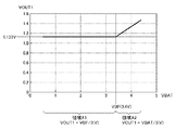
ここで、図4は、図2に示すリニアレギュレーター62から出力される出力電圧VOUT1とバッテリー電圧VBATとの関係の一例を示す図である。図4は、バッテリー電圧VBATがしきい値電圧VBF以上であっても、引き続き、リニアレギュレーター62から出力電圧VOUT1を出力した場合を図示したものである。また、図4では、一例として、しきい値電圧VBFを3.4Vに設定している。
Here, FIG. 4 is a diagram showing an example of the relationship between the output voltage VOUT1 output from the
バッテリー90(充電対象92)のバッテリー電圧VBATがしきい値電圧VBF(所定値)未満である場合、すなわち、図4の領域A1では、リニアレギュレーター62(第1の電源回路)は、出力電圧VOUT1として定電圧で電力を出力する。図4では、横軸に示すバッテリー電圧VBATが3.4V未満である領域A1において、縦軸に示す出力電圧VOUT1が1.133Vで一定に維持されている。 When the battery voltage VBAT of the battery 90 (charge target 92) is less than the threshold voltage VBF (predetermined value), that is, in the region A1 of FIG. 4, the linear regulator 62 (first power supply circuit) has an output voltage VOUT1. Outputs power at a constant voltage. In FIG. 4, in the region A1 where the battery voltage VBAT shown on the horizontal axis is less than 3.4 V, the output voltage VOUT1 shown on the vertical axis is kept constant at 1.133 V.
一方、バッテリー90のバッテリー電圧VBATがしきい値電圧VBF以上である場合、すなわち、図4の領域A2では、リニアレギュレーター62は、バッテリー電圧VBATを所定の降圧比で降圧した電圧で電力を出力する。図4の例では、横軸に示すバッテリー電圧VBATが3.4V以上である領域A2において、縦軸に示す出力電圧VOUT1は、バッテリー電圧VBATに連動してほぼ単調に増加している。この領域A2では、リニアレギュレーター62は、バッテリー電圧VBATに応じた出力電圧VOUT1を生成している。このため、領域A2では、充電の進行に伴ってバッテリー電圧VBATが上昇すると、それに応じて出力電圧VOUT1も上昇することになる。
On the other hand, when the battery voltage VBAT of the
ここで、しきい値電圧VBFの前後では、供給元の切り替えに伴う電圧値の変動が起こりやすい。具体的には、充電系制御回路63の動作例として、領域A1では、リニアレギュレーター62からの出力電圧VOUT1を処理回路100に供給し、領域A2では、チャージポンプ回路711からの出力電圧VOUT2を処理回路100に供給する場合がある。この場合、領域A1では、定電圧である出力電圧VOUT1を、チャージポンプ回路711における降圧比に応じた電圧値に設定するのが好ましい。具体的には、チャージポンプ回路711における降圧比が3分の1である場合、出力電圧VOUT1も、しきい値電圧VBFの3分の1に設定するのが好ましい。このような電圧値に設定されることで、供給元の切り替えを行っても、電圧値が不連続になるのを避けることができ、電圧値の変動を最小限に抑えることができる。これにより、処理回路100の動作が不安定になるのを抑制することができる。
Here, before and after the threshold voltage VBF, the voltage value tends to fluctuate due to the switching of the supply source. Specifically, as an operation example of the charge
図4の例では、リニアレギュレーター62からの出力電圧VOUT1が1.133Vに維持されているが、この電圧値は、3.4/3=1.133という計算式に基づいて算出している。なお、この場合、出力電圧VOUT1は、しきい値電圧VBFの3分の1を中心に、±5%以内程度に設定されるのが好ましく、±3%以内程度に設定されるのがより好ましい。
In the example of FIG. 4, the output voltage VOUT1 from the
また、整流電圧VCCが任意のタイミングで遮断される場合も、上記と同様、遮断の前後で供給元の切り替えが生じることがある。この場合も、上記と同様、領域A1における出力電圧VOUT1を最適化することにより、処理回路100に供給される電圧値の変動を最小限に抑えることができる。
Further, when the rectified voltage VCS is cut off at an arbitrary timing, the supply source may be switched before and after the cutoff, as described above. In this case as well, by optimizing the output voltage VOUT1 in the region A1, the fluctuation of the voltage value supplied to the
3.充放電制御装置の変形例
次に、変形例に係る充放電制御装置10について説明する。
図5は、変形例に係る充放電制御装置の構成を示すブロック図である。
3. 3. Modification Example of Charge / Discharge Control Device Next, the charge /
FIG. 5 is a block diagram showing a configuration of a charge / discharge control device according to a modified example.
以下、変形例に係る充放電制御装置について説明するが、以下の説明では、実施形態に係る充放電制御装置との相違点を中心に説明し、同様の事項についてはその説明を省略する。なお、図5において、図2と同様の構成については、同一の符号を付している。 Hereinafter, the charge / discharge control device according to the modified example will be described, but in the following description, the differences from the charge / discharge control device according to the embodiment will be mainly described, and the description of the same items will be omitted. In FIG. 5, the same reference numerals are given to the same configurations as those in FIG.
図5に示す充放電制御装置10Aは、図2に示すリニアレギュレーター62に代えて、スイッチングレギュレーター62Aを用いていること以外、図2に示す充放電制御装置10と同様である。すなわち、図5に示す充放電制御装置10は、第1の電源回路としてスイッチングレギュレーター62Aを備えている。
The charge /
スイッチングレギュレーター62Aは、例えば、DC−DCコンバーターにより実現される。スイッチングレギュレーター62Aは、リニアレギュレーター62に比べて、消費電力が小さい。このため、電子機器30の低消費電力化を図ることができる。これにより、例えば、整流電圧VCCの電源として、放電量が有限の電池(外部バッテリー)等を利用している場合、その電池の放電量を減らすことができ、より長期間の使用が可能になる。
以上のような変形例においても、前記実施形態と同様の効果が得られる。
The
Even in the above-mentioned modified examples, the same effect as that of the above-described embodiment can be obtained.
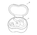
4.電子機器の具体例
図6は、図2に示す電子機器の一例であるイヤホンを示す斜視図である。
4. Specific Example of Electronic Device FIG. 6 is a perspective view showing an earphone which is an example of the electronic device shown in FIG.
図6に示すイヤホン510は、例えば補聴器のイヤホンであってもよいし、オーディオ視聴用のイヤホンであってもよい。図6には図示しないものの、このイヤホン510(電子機器)は、図2に示す充放電制御装置10、バッテリー90および処理回路100を備えている。
The
図6に示すイヤホン510は、充電用のケース600に収納可能である。イヤホン510は、図示しない電源ケーブル等を介してケース600に接続され、電源ケーブルを介して受電するように構成されていてもよいし、無接点の電力伝送により受電するように構成されていてもよい。なお、ケース600は、外部から受電する機能を有していてもよいし、バッテリー90とは別の一次電池または二次電池を有していてもよい。後者の場合、ケース600が有する電池(外部バッテリー)が、前述した整流電圧VCCの電源となる。
The
前述したように、充放電制御装置10は、整流電圧VCCの受電時、バッテリー90の状態によらず、処理回路100に電力を供給することができる。このため、例えば、バッテリー90が過放電状態にあるときでも、イヤホン510を充電用のケース600に収納すれば、処理回路100への電力の供給が可能になり、処理回路100による各種処理を実行させることができる。
As described above, the charge /
これにより、バッテリー90の状態によらず、イヤホン510を充電しながら、イヤホン510を使用することも可能になり、利便性を高めることができる。
As a result, the
また、例えば、イヤホン510が外部機器への通信機能を有している場合、バッテリー90の状態によらず、外部機器との通信を確立する通信処理を処理回路100に実行させることができる。その結果、例えばスマートフォン等の外部機器に充電ステータス等の情報を通知するといった通知処理を、処理回路100に実行させることも可能になり、イヤホン510の利便性を高めることができる。
Further, for example, when the
なお、図2に示す電子機器30としては、例えば図6に示すイヤホン510のようなヒヤラブル機器またはウェアラブル機器の他、ヘッドマウントディスプレイ、スマートフォンや携帯電話機のような携帯型通信端末、腕時計、生体情報測定装置、シェーバー、電動歯ブラシ、リストコンピューター、ハンディターミナル、自動車の車載機器等の種々の機器が挙げられる。
The
以上、本発明の充放電制御装置および電子機器を図示の実施形態に基づいて説明したが、本発明はこれに限定されるものではない。例えば、本発明の充放電制御装置および電子機器は、前記実施形態の各部の構成を、同様の機能を有する任意の構成に置換したものであってもよく、前記実施形態に任意の構成物が付加されたものであってもよい。 Although the charge / discharge control device and the electronic device of the present invention have been described above based on the illustrated embodiment, the present invention is not limited thereto. For example, the charge / discharge control device and the electronic device of the present invention may replace the configuration of each part of the embodiment with an arbitrary configuration having the same function, and any configuration may be used in the embodiment. It may be an added one.
10…充放電制御装置、10A…充放電制御装置、30…電子機器、50…制御回路、60…充電系回路、62…リニアレギュレーター、62A…スイッチングレギュレーター、63…充電系制御回路、65…充電回路、66…A/D変換回路、68…不揮発性メモリー、70…放電系回路、71…給電回路、73…放電系制御回路、74…インターフェース回路、76…レジスター、80…制御部、90…バッテリー、92…充電対象、99…給電対象、100…処理回路、510…イヤホン、600…ケース、711…チャージポンプ回路、A1…領域、A2…領域、ENch…制御信号、ENor…制御信号、S1…ステップ、S2…ステップ、S3…ステップ、S4…ステップ、VBAT…バッテリー電圧、VBF…しきい値電圧、VCC…整流電圧、VOUT1…出力電圧、VOUT2…出力電圧 10 ... Charge / discharge control device, 10A ... Charge / discharge control device, 30 ... Electronic equipment, 50 ... Control circuit, 60 ... Charging system circuit, 62 ... Linear regulator, 62A ... Switching regulator, 63 ... Charging system control circuit, 65 ... Charging Circuit, 66 ... A / D conversion circuit, 68 ... Non-volatile memory, 70 ... Discharge system circuit, 71 ... Power supply circuit, 73 ... Discharge system control circuit, 74 ... Interface circuit, 76 ... Register, 80 ... Control unit, 90 ... Battery, 92 ... Charging target, 99 ... Power supply target, 100 ... Processing circuit, 510 ... Earphone, 600 ... Case, 711 ... Charge pump circuit, A1 ... Area, A2 ... Area, ENch ... Control signal, ENor ... Control signal, S1 ... step, S2 ... step, S3 ... step, S4 ... step, VBAT ... battery voltage, VBF ... threshold voltage, VCS ... rectified voltage, VOUT1 ... output voltage, VOUT2 ... output voltage
Claims (7)
受電電力に基づいて、充電対象を充電する充電回路と、
前記充電対象から出力された放電電力に基づいて、前記給電対象に電力を供給する第2の電源回路と、
前記第1の電源回路および前記第2の電源回路の動作を制御する制御部と、
を備え、
前記充電対象の電圧が所定値未満である場合に、前記制御部は、前記第1の電源回路により、前記給電対象に電力を供給させることを特徴とする充放電制御装置。 A first power supply circuit that supplies power to the power supply target based on the received power,
A charging circuit that charges the charging target based on the received power,
A second power supply circuit that supplies power to the power supply target based on the discharge power output from the charging target, and
A control unit that controls the operation of the first power supply circuit and the second power supply circuit,
With
A charge / discharge control device, characterized in that, when the voltage of the charging target is less than a predetermined value, the control unit supplies electric power to the power feeding target by the first power supply circuit.
前記充電対象の電圧が前記所定値以上である場合に、前記第1の電源回路は、前記充電対象の電圧を所定の降圧比で降圧した電圧を前記電力として出力する請求項1ないし5のいずれか1項に記載の充放電制御装置。 When the voltage to be charged is less than the predetermined value, the first power supply circuit outputs the power at a constant voltage.
Any of claims 1 to 5, wherein when the voltage to be charged is equal to or higher than the predetermined value, the first power supply circuit outputs a voltage obtained by stepping down the voltage to be charged by a predetermined step-down ratio as the electric power. The charge / discharge control device according to item 1.
Priority Applications (3)
| Application Number | Priority Date | Filing Date | Title |
|---|---|---|---|
| JP2020033142A JP2021136816A (en) | 2020-02-28 | 2020-02-28 | Charge/discharge control device and electronic apparatus |
| US17/185,165 US11750011B2 (en) | 2020-02-28 | 2021-02-25 | Charge and discharge control apparatus and electronic device |
| CN202110215610.3A CN113328481B (en) | 2020-02-28 | 2021-02-26 | Charge and discharge control device and electronic equipment |
Applications Claiming Priority (1)
| Application Number | Priority Date | Filing Date | Title |
|---|---|---|---|
| JP2020033142A JP2021136816A (en) | 2020-02-28 | 2020-02-28 | Charge/discharge control device and electronic apparatus |
Publications (1)
| Publication Number | Publication Date |
|---|---|
| JP2021136816A true JP2021136816A (en) | 2021-09-13 |
Family
ID=77414431
Family Applications (1)
| Application Number | Title | Priority Date | Filing Date |
|---|---|---|---|
| JP2020033142A Pending JP2021136816A (en) | 2020-02-28 | 2020-02-28 | Charge/discharge control device and electronic apparatus |
Country Status (3)
| Country | Link |
|---|---|
| US (1) | US11750011B2 (en) |
| JP (1) | JP2021136816A (en) |
| CN (1) | CN113328481B (en) |
Families Citing this family (1)
| Publication number | Priority date | Publication date | Assignee | Title |
|---|---|---|---|---|
| CN114336900B (en) * | 2022-03-08 | 2022-07-22 | 深圳市思远半导体有限公司 | Earphone recognition and charging circuit and method for wireless earphone charging bin |
Family Cites Families (17)
| Publication number | Priority date | Publication date | Assignee | Title |
|---|---|---|---|---|
| JPH06153420A (en) | 1992-11-12 | 1994-05-31 | Sony Corp | Cordless electronic equipment and its charger |
| JPH06253471A (en) | 1993-02-26 | 1994-09-09 | Sanyo Electric Co Ltd | Electrical apparatus with floating charging power-supply |
| JP4137496B2 (en) * | 2002-04-15 | 2008-08-20 | 富士通株式会社 | Remaining amount prediction method |
| US7615965B2 (en) * | 2004-05-14 | 2009-11-10 | O2Micro International Limited | Power management system |
| JP5050415B2 (en) * | 2006-06-15 | 2012-10-17 | ミツミ電機株式会社 | Secondary battery charge / discharge circuit and battery pack |
| JP4769227B2 (en) | 2007-05-30 | 2011-09-07 | 京セラ株式会社 | Charging circuit and portable electronic device |
| JP4943296B2 (en) * | 2007-10-30 | 2012-05-30 | ソニー株式会社 | Battery pack, secondary battery charging method, and charging device |
| JP5348697B2 (en) | 2010-10-22 | 2013-11-20 | Necアクセステクニカ株式会社 | Power path switching method and power path switching circuit |
| JP5615254B2 (en) * | 2011-12-09 | 2014-10-29 | 三菱重工業株式会社 | Charge / discharge control device, charge control method, discharge control method, and program |
| JP2016194841A (en) | 2015-04-01 | 2016-11-17 | リズム時計工業株式会社 | Usb fan device with charge function |
| JP6668799B2 (en) * | 2016-02-12 | 2020-03-18 | セイコーエプソン株式会社 | Electronics |
| JP6845068B2 (en) * | 2017-03-31 | 2021-03-17 | 古河電気工業株式会社 | Power storage system |
| JP6950608B2 (en) * | 2018-03-29 | 2021-10-13 | セイコーエプソン株式会社 | Control device, power receiving device and electronic device |
| TWI697169B (en) * | 2018-06-14 | 2020-06-21 | 美律實業股份有限公司 | Electronic device |
| CN110739732B (en) * | 2018-07-20 | 2022-01-25 | 炬芯科技股份有限公司 | Portable electronic equipment, chip, charging system and charging method thereof |
| US11148546B2 (en) * | 2018-08-07 | 2021-10-19 | Toyota Jidosha Kabushiki Kaisha | Power supply control device |
| US11467463B2 (en) * | 2019-01-29 | 2022-10-11 | Halio, Inc. | Overcharge-aware driver for electrochromic devices |
-
2020
- 2020-02-28 JP JP2020033142A patent/JP2021136816A/en active Pending
-
2021
- 2021-02-25 US US17/185,165 patent/US11750011B2/en active Active
- 2021-02-26 CN CN202110215610.3A patent/CN113328481B/en active Active
Also Published As
| Publication number | Publication date |
|---|---|
| CN113328481B (en) | 2024-06-21 |
| US20210273472A1 (en) | 2021-09-02 |
| US11750011B2 (en) | 2023-09-05 |
| CN113328481A (en) | 2021-08-31 |
Similar Documents
| Publication | Publication Date | Title |
|---|---|---|
| US9362742B2 (en) | Semiconductor integrated circuit and operating method thereof | |
| US7868582B2 (en) | Portable devices having multiple power interfaces | |
| US9231435B2 (en) | Methods and apparatuses for operating devices with solar power | |
| US9276404B2 (en) | Semiconductor integrated circuit and operating method thereof | |
| JP4197189B2 (en) | Circuit for power supply and method of operation | |
| US8482260B2 (en) | Power management system having charging control unit and power switching control unit | |
| JP5912513B2 (en) | Charging circuit and electronic device using the same | |
| US20050242772A1 (en) | Electronic device | |
| JP6053280B2 (en) | Charging circuit and electronic device using the same | |
| JP6362448B2 (en) | Power supply selection circuit, signal processing circuit using the same, and electronic equipment | |
| CN118747028B (en) | Power supply selection circuit, chip and electronic equipment | |
| JP2019175755A (en) | Circuit device, control device, power-receiving device, and electronic equipment | |
| TWI505593B (en) | Configurable power supply system and power supply configuration method | |
| US11750011B2 (en) | Charge and discharge control apparatus and electronic device | |
| US11476696B2 (en) | Charge and discharge control apparatus and electronic device | |
| KR100630964B1 (en) | Adapters and electronics using them | |
| KR102491650B1 (en) | Electronic device for a voltage controlling operating method thereof | |
| JP2005295683A (en) | Portable terminal apparatus | |
| JP7328010B2 (en) | A power receiving device and its control circuit, a method of negotiation between the power feeding device and the power receiving device | |
| EP3674844B1 (en) | Circuit and method of operation for an adaptive charge rate power supply | |
| EP1696571A1 (en) | Battery-operated equipment | |
| KR20130062888A (en) | Power management system suitable for use with multi-series-cell batteries | |
| CN223108315U (en) | A portable computer | |
| CN115459374B (en) | Wireless earphone and circuit thereof, charging box and circuit thereof, and wireless earphone assembly | |
| JP2023541143A (en) | Battery management device and battery pack including it |
Legal Events
| Date | Code | Title | Description |
|---|---|---|---|
| RD07 | Notification of extinguishment of power of attorney |
Free format text: JAPANESE INTERMEDIATE CODE: A7427 Effective date: 20200827 |
|
| RD04 | Notification of resignation of power of attorney |
Free format text: JAPANESE INTERMEDIATE CODE: A7424 Effective date: 20210922 |
|
| RD03 | Notification of appointment of power of attorney |
Free format text: JAPANESE INTERMEDIATE CODE: A7423 Effective date: 20211104 |