JP2021069089A - Power amplifier module and power amplifying method - Google Patents
Power amplifier module and power amplifying method Download PDFInfo
- Publication number
- JP2021069089A JP2021069089A JP2019195308A JP2019195308A JP2021069089A JP 2021069089 A JP2021069089 A JP 2021069089A JP 2019195308 A JP2019195308 A JP 2019195308A JP 2019195308 A JP2019195308 A JP 2019195308A JP 2021069089 A JP2021069089 A JP 2021069089A
- Authority
- JP
- Japan
- Prior art keywords
- bias
- transistor
- circuit
- power
- operation mode
- Prior art date
- Legal status (The legal status is an assumption and is not a legal conclusion. Google has not performed a legal analysis and makes no representation as to the accuracy of the status listed.)
- Pending
Links
Images


Classifications
-
- H—ELECTRICITY
- H03—ELECTRONIC CIRCUITRY
- H03F—AMPLIFIERS
- H03F3/00—Amplifiers with only discharge tubes or only semiconductor devices as amplifying elements
- H03F3/20—Power amplifiers, e.g. Class B amplifiers, Class C amplifiers
-
- H—ELECTRICITY
- H03—ELECTRONIC CIRCUITRY
- H03F—AMPLIFIERS
- H03F1/00—Details of amplifiers with only discharge tubes, only semiconductor devices or only unspecified devices as amplifying elements
- H03F1/02—Modifications of amplifiers to raise the efficiency, e.g. gliding Class A stages, use of an auxiliary oscillation
- H03F1/0205—Modifications of amplifiers to raise the efficiency, e.g. gliding Class A stages, use of an auxiliary oscillation in transistor amplifiers
- H03F1/0211—Modifications of amplifiers to raise the efficiency, e.g. gliding Class A stages, use of an auxiliary oscillation in transistor amplifiers with control of the supply voltage or current
- H03F1/0216—Continuous control
- H03F1/0222—Continuous control by using a signal derived from the input signal
-
- H—ELECTRICITY
- H03—ELECTRONIC CIRCUITRY
- H03F—AMPLIFIERS
- H03F1/00—Details of amplifiers with only discharge tubes, only semiconductor devices or only unspecified devices as amplifying elements
- H03F1/02—Modifications of amplifiers to raise the efficiency, e.g. gliding Class A stages, use of an auxiliary oscillation
- H03F1/0205—Modifications of amplifiers to raise the efficiency, e.g. gliding Class A stages, use of an auxiliary oscillation in transistor amplifiers
- H03F1/0261—Modifications of amplifiers to raise the efficiency, e.g. gliding Class A stages, use of an auxiliary oscillation in transistor amplifiers with control of the polarisation voltage or current, e.g. gliding Class A
- H03F1/0266—Modifications of amplifiers to raise the efficiency, e.g. gliding Class A stages, use of an auxiliary oscillation in transistor amplifiers with control of the polarisation voltage or current, e.g. gliding Class A by using a signal derived from the input signal
-
- H—ELECTRICITY
- H03—ELECTRONIC CIRCUITRY
- H03F—AMPLIFIERS
- H03F1/00—Details of amplifiers with only discharge tubes, only semiconductor devices or only unspecified devices as amplifying elements
- H03F1/30—Modifications of amplifiers to reduce influence of variations of temperature or supply voltage or other physical parameters
- H03F1/302—Modifications of amplifiers to reduce influence of variations of temperature or supply voltage or other physical parameters in bipolar transistor amplifiers
-
- H—ELECTRICITY
- H03—ELECTRONIC CIRCUITRY
- H03F—AMPLIFIERS
- H03F3/00—Amplifiers with only discharge tubes or only semiconductor devices as amplifying elements
- H03F3/189—High frequency amplifiers, e.g. radio frequency amplifiers
- H03F3/19—High frequency amplifiers, e.g. radio frequency amplifiers with semiconductor devices only
- H03F3/195—High frequency amplifiers, e.g. radio frequency amplifiers with semiconductor devices only in integrated circuits
-
- H—ELECTRICITY
- H03—ELECTRONIC CIRCUITRY
- H03F—AMPLIFIERS
- H03F3/00—Amplifiers with only discharge tubes or only semiconductor devices as amplifying elements
- H03F3/20—Power amplifiers, e.g. Class B amplifiers, Class C amplifiers
- H03F3/21—Power amplifiers, e.g. Class B amplifiers, Class C amplifiers with semiconductor devices only
- H03F3/211—Power amplifiers, e.g. Class B amplifiers, Class C amplifiers with semiconductor devices only using a combination of several amplifiers
-
- H—ELECTRICITY
- H03—ELECTRONIC CIRCUITRY
- H03F—AMPLIFIERS
- H03F3/00—Amplifiers with only discharge tubes or only semiconductor devices as amplifying elements
- H03F3/20—Power amplifiers, e.g. Class B amplifiers, Class C amplifiers
- H03F3/24—Power amplifiers, e.g. Class B amplifiers, Class C amplifiers of transmitter output stages
- H03F3/245—Power amplifiers, e.g. Class B amplifiers, Class C amplifiers of transmitter output stages with semiconductor devices only
-
- H—ELECTRICITY
- H03—ELECTRONIC CIRCUITRY
- H03F—AMPLIFIERS
- H03F3/00—Amplifiers with only discharge tubes or only semiconductor devices as amplifying elements
- H03F3/30—Single-ended push-pull [SEPP] amplifiers; Phase-splitters therefor
- H03F3/3001—Single-ended push-pull [SEPP] amplifiers; Phase-splitters therefor with field-effect transistors
- H03F3/3022—CMOS common source output SEPP amplifiers
- H03F3/3028—CMOS common source output SEPP amplifiers with symmetrical driving of the end stage
- H03F3/303—CMOS common source output SEPP amplifiers with symmetrical driving of the end stage using opamps as driving stages
-
- H—ELECTRICITY
- H03—ELECTRONIC CIRCUITRY
- H03F—AMPLIFIERS
- H03F2200/00—Indexing scheme relating to amplifiers
- H03F2200/411—Indexing scheme relating to amplifiers the output amplifying stage of an amplifier comprising two power stages
-
- H—ELECTRICITY
- H03—ELECTRONIC CIRCUITRY
- H03F—AMPLIFIERS
- H03F2200/00—Indexing scheme relating to amplifiers
- H03F2200/451—Indexing scheme relating to amplifiers the amplifier being a radio frequency amplifier
-
- H—ELECTRICITY
- H03—ELECTRONIC CIRCUITRY
- H03F—AMPLIFIERS
- H03F2200/00—Indexing scheme relating to amplifiers
- H03F2200/504—Indexing scheme relating to amplifiers the supply voltage or current being continuously controlled by a controlling signal, e.g. the controlling signal of a transistor implemented as variable resistor in a supply path for, an IC-block showed amplifier
-
- H—ELECTRICITY
- H03—ELECTRONIC CIRCUITRY
- H03F—AMPLIFIERS
- H03F2200/00—Indexing scheme relating to amplifiers
- H03F2200/516—Some amplifier stages of an amplifier use supply voltages of different value
-
- Y—GENERAL TAGGING OF NEW TECHNOLOGICAL DEVELOPMENTS; GENERAL TAGGING OF CROSS-SECTIONAL TECHNOLOGIES SPANNING OVER SEVERAL SECTIONS OF THE IPC; TECHNICAL SUBJECTS COVERED BY FORMER USPC CROSS-REFERENCE ART COLLECTIONS [XRACs] AND DIGESTS
- Y02—TECHNOLOGIES OR APPLICATIONS FOR MITIGATION OR ADAPTATION AGAINST CLIMATE CHANGE
- Y02D—CLIMATE CHANGE MITIGATION TECHNOLOGIES IN INFORMATION AND COMMUNICATION TECHNOLOGIES [ICT], I.E. INFORMATION AND COMMUNICATION TECHNOLOGIES AIMING AT THE REDUCTION OF THEIR OWN ENERGY USE
- Y02D30/00—Reducing energy consumption in communication networks
- Y02D30/70—Reducing energy consumption in communication networks in wireless communication networks
Abstract
Description
本発明は、電力増幅モジュール及び電力増幅方法に関する。 The present invention relates to a power amplification module and a power amplification method.
携帯端末等の移動体通信機においては、基地局へ送信する信号の電力を増幅するために電力増幅モジュールが用いられる。携帯端末等においては、通信可能時間を長くするために消費電力を低減することが求められる。消費電力の低減を図るために、携帯端末等の電力増幅モジュールに、エンベロープトラッキング方式(ET方式)が採用される場合がある。また、低電力動作時には、入力振幅と出力振幅との関係(AM−AM)の線形性を向上させるために、平均電力トラッキング方式(APT方式)が採用される場合がある。このように、1つの増幅回路が、ET方式で動作するモードと、APT方式で動作するモードとを備える場合がある。 In mobile communication devices such as mobile terminals, a power amplification module is used to amplify the power of a signal transmitted to a base station. In mobile terminals and the like, it is required to reduce power consumption in order to prolong the communicable time. In order to reduce power consumption, an envelope tracking method (ET method) may be adopted for a power amplification module of a mobile terminal or the like. Further, during low power operation, an average power tracking method (APT method) may be adopted in order to improve the linearity of the relationship between the input amplitude and the output amplitude (AM-AM). In this way, one amplifier circuit may include a mode that operates in the ET system and a mode that operates in the APT system.
下記の特許文献1に、ET方式で動作するモードとAPT方式で動作するモードとを備えた電力増幅モジュールが開示されている。この電力増幅モジュールのバイアス回路は、バイアス用の電源からベースバラスト抵抗を介して増幅トランジスタのベースにバイアス電流を供給する。バイアス回路は、電力増幅モジュールの動作モードに応じて、ベースバラスト抵抗の抵抗値を異ならせる機能を持つ。
APT方式で動作する電力増幅モジュールが、動作モードとして低出力モードと高出力モードとを備える場合がある。例えば、出力信号レベルに応じて動作モードが低出力モードと高出力モードとの間で切り替えられる。低出力モードと高出力モードとでは、バイアス回路のベースバラスト抵抗の抵抗値が異なる。 A power amplification module operating in the APT system may have a low output mode and a high output mode as operation modes. For example, the operation mode can be switched between the low output mode and the high output mode according to the output signal level. The resistance value of the base ballast resistor of the bias circuit differs between the low output mode and the high output mode.
上述のように、2つの動作モードを切り替えて動作する機能を備えた従来の電力増幅モジュールにおいては、動作モードに応じてバイアス回路のベースバラスト抵抗の抵抗値が切り替えられる。 As described above, in the conventional power amplification module having a function of switching between the two operation modes, the resistance value of the base ballast resistor of the bias circuit is switched according to the operation mode.
2つの動作モードの各々において電力増幅モジュールの特性に対する要求が厳しくなると、バイアス回路のベースバラスト抵抗の抵抗値を切り替えるのみでは、要求に十分応えることが困難である。本発明の目的は、少なくとも2つの動作モードで動作する機能を持つ電力増幅モジュールの2つの動作モードの各々における特性を十分引き出すことを可能にする電力増幅モジュールを提供することである。本発明の他の目的は、この電力増幅モジュールを用いた電力増幅方法を提供することである。 When the requirements for the characteristics of the power amplification module become strict in each of the two operation modes, it is difficult to sufficiently meet the requirements simply by switching the resistance value of the base ballast resistor of the bias circuit. An object of the present invention is to provide a power amplification module capable of sufficiently drawing out the characteristics in each of the two operation modes of a power amplification module having a function of operating in at least two operation modes. Another object of the present invention is to provide a power amplification method using this power amplification module.
本発明の一観点によると、
入力信号を増幅して出力し、特性が異なる少なくとも2つの動作モードで動作する増幅トランジスタと、
第1バイアス供給トランジスタを含み、前記第1バイアス供給トランジスタの出力電流を、前記増幅トランジスタにバイアス電流として供給する第1バイアス回路と、
第2バイアス供給トランジスタを含み、前記第2バイアス供給トランジスタの出力電流の一部を、前記増幅トランジスタにバイアス電流として供給する第2バイアス回路と、
前記増幅トランジスタの動作モードに応じて、前記第1バイアス回路及び前記第2バイアス回路の少なくとも一方を選択して動作させるバイアス制御信号が入力されるバイアス制御端子と
を有し、
前記第2バイアス回路は、前記第2バイアス供給トランジスタの出力電流の一部を前記第2バイアス回路に戻す電流路を含む電力増幅モジュールが提供される。
According to one aspect of the invention
An amplification transistor that amplifies and outputs the input signal and operates in at least two operating modes with different characteristics.
A first bias circuit that includes a first bias supply transistor and supplies the output current of the first bias supply transistor to the amplification transistor as a bias current.
A second bias circuit including a second bias supply transistor and supplying a part of the output current of the second bias supply transistor to the amplification transistor as a bias current.
It has a bias control terminal to which a bias control signal for selecting and operating at least one of the first bias circuit and the second bias circuit is input according to the operation mode of the amplification transistor.
The second bias circuit is provided with a power amplification module including a current path that returns a part of the output current of the second bias supply transistor to the second bias circuit.
本発明の他の観点によると、
入力信号を増幅して出力する増幅トランジスタと、
第1バイアス供給トランジスタを含み、前記第1バイアス供給トランジスタの出力電流をバイアス電流として前記増幅トランジスタに供給する第1バイアス回路と、
第2バイアス供給トランジスタを含み、前記第2バイアス供給トランジスタの出力電流の一部をバイアス電流として前記増幅トランジスタに供給する第2バイアス回路と
を有し、
前記第2バイアス回路は、前記第2バイアス供給トランジスタの出力電流の一部を前記第2バイアス回路に戻す電流路を含む電力増幅モジュールを動作させて電力増幅を行う方法であって、
前記増幅トランジスタをエンベロープトラッキング方式で動作させるときに、前記第1バイアス回路から前記増幅トランジスタにバイアス電流を供給し、
前記増幅トランジスタを平均電力トラッキング方式で動作させるときに、前記第2バイアス回路から前記増幅トランジスタにバイアス電流を供給する電力増幅方法が提供される。
According to another aspect of the invention
An amplification transistor that amplifies and outputs an input signal,
A first bias circuit including a first bias supply transistor and supplying the output current of the first bias supply transistor as a bias current to the amplification transistor.
It includes a second bias supply transistor, and has a second bias circuit that supplies a part of the output current of the second bias supply transistor as a bias current to the amplification transistor.
The second bias circuit is a method of performing power amplification by operating a power amplification module including a current path that returns a part of the output current of the second bias supply transistor to the second bias circuit.
When the amplification transistor is operated by the envelope tracking method, a bias current is supplied to the amplification transistor from the first bias circuit.
A power amplification method for supplying a bias current to the amplification transistor from the second bias circuit when the amplification transistor is operated by the average power tracking method is provided.
本発明のさらに他の観点によると、
入力信号を増幅して出力する増幅トランジスタと、
第1バイアス供給トランジスタを含み、前記第1バイアス供給トランジスタの出力電流をバイアス電流として前記増幅トランジスタに供給する第1バイアス回路と、
第2バイアス供給トランジスタを含み、前記第2バイアス供給トランジスタの出力電流の一部をバイアス電流として前記増幅トランジスタに供給する第2バイアス回路と
を有し、
前記第2バイアス回路は、前記第2バイアス供給トランジスタの出力電流の一部を前記第2バイアス回路に戻す電流路を含む電力増幅モジュールを動作させて電力増幅を行う方法であって、
前記増幅トランジスタから出力される信号レベルに応じて、前記第1バイアス回路から前記増幅トランジスタにバイアス電流を供給する状態と、前記第1バイアス回路及び前記第2バイアス回路の両方から前記増幅トランジスタにバイアス電流を供給する状態とを切り替える電力増幅方法が提供される。
According to yet another aspect of the invention.
An amplification transistor that amplifies and outputs an input signal,
A first bias circuit including a first bias supply transistor and supplying the output current of the first bias supply transistor as a bias current to the amplification transistor.
It includes a second bias supply transistor, and has a second bias circuit that supplies a part of the output current of the second bias supply transistor as a bias current to the amplification transistor.
The second bias circuit is a method of performing power amplification by operating a power amplification module including a current path that returns a part of the output current of the second bias supply transistor to the second bias circuit.
Depending on the signal level output from the amplification transistor, the bias current is supplied from the first bias circuit to the amplification transistor, and both the first bias circuit and the second bias circuit bias the amplification transistor. A power amplification method for switching between a current supply state and a current supply state is provided.
第2バイアス供給トランジスタの出力電流の一部が、電流路を通って第2バイアス回路に戻されるため、戻される電流によって帰還制御を行うことができる。増幅トランジスタの動作モードに応じて、第1バイアス回路と、帰還制御を行うことが可能な第2バイアス回路との少なくとも一方を選択して動作させることにより、各動作モードの特性をより好適化することが可能になる。 Since a part of the output current of the second bias supply transistor is returned to the second bias circuit through the current path, feedback control can be performed by the returned current. By selecting and operating at least one of the first bias circuit and the second bias circuit capable of performing feedback control according to the operation mode of the amplification transistor, the characteristics of each operation mode are further optimized. Will be possible.
[第1実施例]
図1から図4までの図面を参照して、第1実施例による電力増幅モジュールについて説明する。
[First Example]
The power amplification module according to the first embodiment will be described with reference to the drawings of FIGS. 1 to 4.
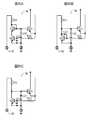
図1は、第1実施例による電力増幅モジュールに用いられる増幅回路素子45の等価回路図である。増幅回路素子45は、パワー段増幅回路10、ドライバ段増幅回路11、パワー段用の第1バイアス回路20と第2バイアス回路30、ドライバ段用のドライバ段バイアス回路40を含む。増幅回路素子45は、さらに、入力側インピーダンス整合回路12、段間インピーダンス整合回路13、複数の外部端子81、82、83、84、85、86、87、及び接地用の複数の外部端子を含む。複数の外部端子81、82、83、84、85、86、87、及び接地用の複数の外部端子には、例えばCuピラーバンプが用いられる。これらの複数の構成要素は、例えば1枚の半導体チップ上に形成される。図1において、接地用の外部端子には参照符号を付していない。
FIG. 1 is an equivalent circuit diagram of an
外部端子85から高周波入力信号RFinが入力される。高周波入力信号RFinは、入力側インピーダンス整合回路12を介してドライバ段増幅回路11に入力される。ドライバ段増幅回路11で増幅された信号が段間インピーダンス整合回路13を介してパワー段増幅回路10に入力される。パワー段増幅回路10で増幅された信号Poutが外部端子87から出力される。
The high frequency input signal RFin is input from the
パワー段増幅回路10は、増幅トランジスタQ1、DCカットキャパシタC1及びベースバラスト抵抗R1を含む。増幅トランジスタQ1は、相互に並列に接続された複数のトランジスタセルで構成される。DCカットキャパシタC1及びベースバラスト抵抗R1は、トランジスタセルごとに設けられている。増幅トランジスタQ1のエミッタが接地されている。増幅トランジスタQ1のコレクタが外部端子87に接続されている。複数のトランジスタセルの各々は、例えばヘテロ接合バイポーラトランジスタ(HBT)で構成される。
The power
DCカットキャパシタC1は、増幅トランジスタQ1のベースに接続されており、ドライバ段増幅回路11で増幅された高周波信号が、DCカットキャパシタC1を介して増幅トランジスタQ1のベースに入力される。ベースバイアス電流が、第1バイアス回路20及び第2バイアス回路30からベースバラスト抵抗R1を介して増幅トランジスタQ1のベースに供給される。外部端子87から増幅トランジスタQ1のコレクタに電源電圧が供給される。
The DC cut capacitor C1 is connected to the base of the amplification transistor Q1, and the high frequency signal amplified by the driver
ドライバ段増幅回路11は、増幅トランジスタQ2、DCカットキャパシタC2及びベースバラスト抵抗R2を含み、パワー段増幅回路10と同様の構成を有する。外部端子86から増幅トランジスタQ2のコレクタに電源電圧Vcc2が供給される。
The driver
第1バイアス回路20及び第2バイアス回路30は、ベースバラスト抵抗R1を介して増幅トランジスタQ1のベースにバイアス電流を供給する。ドライバ段バイアス回路40は、ベースバラスト抵抗R2を介して増幅トランジスタQ2のベースにバイアス電流を供給する。
The
次に、第1バイアス回路20の回路構成について説明する。第1バイアス回路20は、第1バイアス供給トランジスタQ11、トランジスタQ12、Q13を含む。第1バイアス供給トランジスタQ11、トランジスタQ12、Q13は、一例として、ヘテロ接合バイポーラトランジスタである。
Next, the circuit configuration of the
第1バイアス供給トランジスタQ11のコレクタが外部端子84に接続されている。外部端子84に、バイアス電源電圧Vbatが印加されることにより、第1バイアス供給トランジスタQ11のコレクタにバイアス電源電圧Vbatが印加される。第1バイアス供給トランジスタQ11のエミッタが、出力抵抗R12を介してベースバラスト抵抗R1に接続されている。なお、出力抵抗R12は省略してもよい。第1バイアス供給トランジスタQ11は、エミッタフォロワ回路を構成しており、全エミッタ電流がバイアス電流として増幅トランジスタQ1に供給される。本明細書において第1バイアス回路20のように全エミッタ電流がバイアス電流として増幅トランジスタQ1に供給される回路を「エミッタフォロワ型バイアス回路」という。
The collector of the first bias supply transistor Q11 is connected to the
トランジスタQ12、Q13の各々において、ベースとコレクタとが短絡されている。ベースとコレクタとが短絡された接続形態はダイオード接続と呼ばれ、トランジスタQ12、Q13はダイオードとして動作する。 In each of the transistors Q12 and Q13, the base and the collector are short-circuited. The connection form in which the base and collector are short-circuited is called a diode connection, and the transistors Q12 and Q13 operate as diodes.
外部端子81とグランドとの間に、抵抗R11、トランジスタQ12、Q13が、この順番に直列に挿入されている。トランジスタQ12、Q13からなるダイオードに、順方向の電圧が印加される。外部端子81は可変電流源に接続される。この可変電流源は、例えばパワー段増幅回路10の出力電力に応じた電流量のバイアス制御信号IB1を生成して出力する。トランジスタQ12、Q13がダイオードとして動作するため、トランジスタQ12のコレクタ及びベースに所定レベルの電圧(例えば2.6V程度)が発生する。
A resistor R11, transistors Q12, and Q13 are inserted in series between the
第1バイアス供給トランジスタQ11のベースとトランジスタQ12のベースとが相互に接続されている。また、第1バイアス供給トランジスタQ11のベース及びトランジスタQ12のベースは、バイパスキャパシタC11を介して接地される。 The base of the first bias supply transistor Q11 and the base of the transistor Q12 are connected to each other. Further, the base of the first bias supply transistor Q11 and the base of the transistor Q12 are grounded via the bypass capacitor C11.
次に、第1バイアス回路20の動作について説明する。
外部端子81に接続された可変電流源からバイアス制御信号IB1を供給すると、トランジスタQ12、Q13の直列回路に発生する電圧降下に相当する電圧が、第1バイアス供給トランジスタQ11のベースに印加される。第1バイアス供給トランジスタQ11のベースに印加される電圧に応じて、第1バイアス供給トランジスタQ11にエミッタ電流(出力電流)が流れる。このエミッタ電流が、出力抵抗R12及びベースバラスト抵抗R1を介して、増幅トランジスタQ1のベースに、バイアス電流として供給される。
Next, the operation of the
When the bias control signal IB1 is supplied from the variable current source connected to the
外部端子81にバイアス制御信号IB1が供給されない状態では、第1バイアス供給トランジスタQ11はオフになる。このため、第1バイアス回路20からは、増幅トランジスタQ1のベースにバイアス電流が供給されない。
When the bias control signal IB1 is not supplied to the
次に、第2バイアス回路30の回路構成について説明する。第2バイアス回路30は、第2バイアス供給トランジスタQ21、トランジスタQ22、Q23を含む。第2バイアス供給トランジスタQ21、トランジスタQ22、Q23は、一例として、ヘテロ接合バイポーラトランジスタである。
Next, the circuit configuration of the
第2バイアス供給トランジスタQ21のコレクタが外部端子84に接続されており、第2バイアス供給トランジスタQ21のコレクタに、バイアス電源電圧Vbatが印加される。第2バイアス供給トランジスタQ21のエミッタが、ベースバラスト抵抗R1に接続されるとともに、抵抗R22を介してトランジスタQ23のベースに接続されている。抵抗R22は、第2バイアス供給トランジスタQ21のエミッタ電流の一部を第2バイアス回路30に戻す電流路として機能する。本明細書において、第2バイアス回路30のように、第2バイアス供給トランジスタQ21のエミッタ電流の一部を第2バイアス回路30に戻す電流路を備えた回路を「フィードバック型バイアス回路」という。
The collector of the second bias supply transistor Q21 is connected to the
トランジスタQ22がダイオード接続されており、ダイオードとして動作する。トランジスタQ23のベースとコレクタとが、キャパシタC22により接続されている。外部端子82とグランドとの間に、抵抗R21、トランジスタQ22、Q23が、この順番に直列に挿入されている。トランジスタQ22、Q23のいずれも、エミッタが接地側になる向きに接続されている。
The transistor Q22 is connected to a diode and operates as a diode. The base and collector of the transistor Q23 are connected by a capacitor C22. A resistor R21, transistors Q22, and Q23 are inserted in series between the
外部端子82は可変電流源に接続されており、外部端子82から抵抗R21に、一定の電流であるバイアス制御信号IB2が供給される。第2バイアス供給トランジスタQ21のベースとトランジスタQ22のベースとが相互に接続されている。また、第2バイアス供給トランジスタQ21のベース及びトランジスタQ22のベースは、バイパスキャパシタC21を介して接地されている。
The
次に、第2バイアス回路30の動作について説明する。
外部端子82に接続された可変電流源からバイアス制御信号IB2を供給すると、トランジスタQ22、Q23の直列回路に発生する電圧降下に相当する電圧が、第2バイアス供給トランジスタQ21のベースに印加される。第2バイアス供給トランジスタQ21のベースに印加される電圧に応じて、第2バイアス供給トランジスタQ21にエミッタ電流(出力電流)が流れる。このエミッタ電流の一部が、ベースバラスト抵抗R1を介して、増幅トランジスタQ1のベースに、バイアス電流として供給される。
Next, the operation of the
When the bias control signal IB2 is supplied from the variable current source connected to the
増幅トランジスタQ1の出力電力が増大すると、第2バイアス供給トランジスタQ21のエミッタから増幅トランジスタQ1のベースに供給されるバイアス電流が増加し、第2バイアス供給トランジスタQ21のエミッタ電圧が上昇する。このとき、抵抗R22を経由してトランジスタQ23のベース電圧も上昇する。これにより、トランジスタQ23を流れる電流が増加し、トランジスタQ22のコレクタ電圧が低下する。これに伴い、第2バイアス供給トランジスタQ21のベース電圧が低下し、第2バイアス供給トランジスタQ21を流れる電流が減少する。 When the output power of the amplification transistor Q1 increases, the bias current supplied from the emitter of the second bias supply transistor Q21 to the base of the amplification transistor Q1 increases, and the emitter voltage of the second bias supply transistor Q21 rises. At this time, the base voltage of the transistor Q23 also rises via the resistor R22. As a result, the current flowing through the transistor Q23 increases, and the collector voltage of the transistor Q22 decreases. Along with this, the base voltage of the second bias supply transistor Q21 decreases, and the current flowing through the second bias supply transistor Q21 decreases.
このように、第2バイアス回路30は、増幅トランジスタQ1の出力電力が増大して第2バイアス供給トランジスタQ21のエミッタ電流が増加すると、抵抗R22を介して、第2バイアス供給トランジスタQ21のエミッタ電流を低減させる負帰還制御が行われる。このため、第2バイアス供給トランジスタQ21のエミッタ電流が安定する。
As described above, when the output power of the amplification transistor Q1 increases and the emitter current of the second bias supply transistor Q21 increases, the
外部端子82にバイアス制御信号IB2が供給されない状態では、第2バイアス供給トランジスタQ21はオフになる。このため、第2バイアス回路30からは、増幅トランジスタQ1のベースにバイアス電流が供給されない。
When the bias control signal IB2 is not supplied to the
キャパシタC22は、パワー段増幅回路10から流入する高周波信号を、トランジスタQ23を介して交流的に接地する。これにより、トランジスタQ23のベース電流が高周波信号の影響を受けにくくなる。
The capacitor C22 ACly grounds the high-frequency signal flowing from the power
次に、ドライバ段バイアス回路40の回路構成について説明する。ドライバ段バイアス回路40は、バイアス供給トランジスタQ31、抵抗R31、トランジスタQ32、Q33、バイパスキャパシタC31を含む。基本的な回路構成は、第1バイアス回路20の回路構成と同一である。
Next, the circuit configuration of the driver
外部端子83に接続された可変電流源から抵抗R31に、バイアス制御信号IB3が供給される。バイアス供給トランジスタQ31のエミッタ電流が、ドライバ段増幅回路11の増幅トランジスタQ2のベースに、バイアス電流として供給される。
The bias control signal IB3 is supplied to the resistor R31 from the variable current source connected to the
図2は、第1実施例による電力増幅モジュール50のブロック図である。第1実施例による電力増幅モジュール50は、増幅回路素子45(図1)、出力側インピーダンス整合回路60、インダクタL1、L2を含む。図2において、増幅回路素子45の一部の構成要素の記載を省略している。増幅回路素子45、出力側インピーダンス整合回路60、インダクタL1、L2等は、共通のモジュール基板に実装される。電力増幅モジュール50は、モジュール基板に設けられたバイアス制御端子51、52、53、ドライバ段電源端子54、パワー段電源端子55、信号入力端子56、及び信号出力端子57を備えている。
FIG. 2 is a block diagram of the
増幅回路素子45の外部端子85が信号入力端子56に接続されている。信号入力端子56から増幅回路素子45に高周波入力信号RFinが入力される。増幅回路素子45の外部端子83にバイアス制御端子53が接続されている。バイアス制御端子53から増幅回路素子45のドライバ段バイアス回路40にバイアス制御信号IB3が供給される。増幅回路素子45の外部端子86がインダクタL2を介してドライバ段電源端子54に接続されている。ドライバ段増幅回路11の増幅トランジスタQ2のコレクタに、インダクタL2を介して電源電圧Vcc2が供給される。
The
増幅回路素子45の外部端子81、82、83が、それぞれバイアス制御端子51、52、53に接続されている。バイアス制御端子51、52、53は、外部のバイアス制御回路70に接続されている。バイアス制御回路70は、動作モード通知端子71を備えている。バイアス制御回路70は、動作モード通知端子71に与えられる動作モード通知信号MODEに基づいて、バイアス制御端子51、52の少なくとも一方を選択する。バイアス制御回路70は、バイアス制御端子51を選択すると、第1バイアス回路20にバイアス制御信号IB1を供給し、バイアス制御端子52を選択すると、第2バイアス回路30にバイアス制御信号IB2を供給する。さらに、バイアス制御回路70は、バイアス制御端子53及び外部端子83を介してドライバ段バイアス回路40にバイアス制御信号IB3を供給する。
The
増幅回路素子45の外部端子87が、インダクタL1を介してパワー段電源端子55に接続されている。パワー段増幅回路10の増幅トランジスタQ1のコレクタに、インダクタL1を介して電源電圧Vregが供給される。外部端子87は、さらに、出力側インピーダンス整合回路60を介して信号出力端子57に接続されている。パワー段増幅回路10で増幅された高周波信号が、高周波出力信号RFoutとして信号出力端子57から出力される。
The
図3は、第1実施例による電力増幅モジュール50を用いた送信モジュールのブロック図である。この送信モジュールは、ベースバンド部90、高周波部91、電力増幅モジュール50、フロントエンド部92、アンテナ93、バイアス制御回路70、及び電源回路94を備えている。
FIG. 3 is a block diagram of a transmission module using the
ベースバンド部90は、音声やデータ等の入力信号を所定の変調方式に基づいて変調し、変調信号を出力する。例えば、ベースバンド部90は入力信号を直交変調し、変調信号としてIQ信号(I信号とQ信号)を出力する。さらに、ベースバンド部90は、電力増幅モジュール50の動作モードを指令する動作モード通知信号MODEを、バイアス制御回路70及び電源回路94に出力する。
The
例えば、動作モード通知信号MODEによって、電力増幅モジュール50のパワー段増幅回路10(図1、図2)をエンベロープトラッキング方式(ET方式)で動作させる第1動作モード、及び平均電力トラッキング方式(APT方式)で動作させる第2動作モードのいずれか一方が通知される。ベースバンド部90は、例えば、電力増幅モジュール50のパワー段増幅回路10(図1、図2)の出力レベルが所定レベル以上になる場合は、ET方式の第1動作モードを通知し、電力増幅モジュール50の出力レベルが所定レベル未満になる場合は、APT方式の第2動作モードを通知する。
For example, the first operation mode in which the power stage amplifier circuit 10 (FIGS. 1 and 2) of the
高周波部91は、ベースバンド部90から入力されたIQ信号から、無線送信を行うための高周波入力信号RFinを生成し、電力増幅モジュール50に出力する。電力増幅モジュール50は、動作モードに応じて高周波入力信号RFinを増幅し、高周波出力信号RFoutをフロントエンド部92に出力する。ET方式の第1動作モードで動作する場合には、パワー段増幅回路10(図1、図2)は、エミッタフォロワ型の第1バイアス回路20からバイアス電流の供給を受け、APT方式の第2動作モードで動作する場合には、フィードバック型の第2バイアス回路30からバイアス電流の供給を受ける。
The
電源回路94は、動作モード通知信号MODEに応じて、ET方式用の第1電源電圧及びAPT方式用の第2電源電圧の一方を、電源電圧Vregとして電力増幅モジュール50に供給する。電源回路94には、電源電圧Vcc1が供給される。
The
電源電圧Vregを制御するための電圧制御信号CTR1、CTR2が、ベースバンド部90から電源回路94に供給される。電力増幅モジュール50をET方式の第1動作モードで動作させる場合には、ベースバンド部90は、変調信号の振幅レベルを検出し、変調信号の振幅レベルの変化に応じた電圧制御信号CTR1を電源回路94に出力する。電力増幅モジュール50をAPT方式の第2動作モードで動作させる場合には、ベースバンド部90は、変調信号の平均パワーを検出し、変調信号の平均パワーに応じた電圧制御信号CTR2を電源回路94に出力する。
The voltage control signals CTR1 and CTR2 for controlling the power supply voltage Vreg are supplied from the
電源回路94は、動作モード通知信号MODEでET方式の第1動作モードが通知された場合には、電圧制御信号CTR1に基づいて、変調信号の振幅レベルの変化に追随させて電源電圧Vregを変化させる。動作モード通知信号MODEでAPT方式の第2動作モードが通知された場合には、電源回路94は、電圧制御信号CTR2に基づいて、変調信号の平均パワーに応じて電源電圧Vregを変化させる。
When the first operation mode of the ET method is notified by the operation mode notification signal MODE, the
バイアス制御回路70は、動作モード通知信号MODEによってET方式の第1動作モードが通知されている場合には、第1バイアス回路20(図1、図2)にバイアス制御信号IB1を供給し、第2バイアス回路30(図1、図2)には、バイアス制御信号IB2を供給しない。動作モード通知信号MODEによってAPT方式の第2動作モードが通知されている場合には、第2バイアス回路30(図1、図2)にバイアス制御信号IB2を供給し、第1バイアス回路20(図1、図2)には、バイアス制御信号IB1を供給しない。
When the first operation mode of the ET method is notified by the operation mode notification signal MODE, the
フロントエンド部92は、入力された高周波出力信号RFoutに対するフィルタ処理を行う。フロントエンド部92から出力された高周波信号は、アンテナ93から送信される。また、フロントエンド部92は、アンテナ93で受信された高周波受信信号と、送信する高周波信号との送受信の切り替えを行う。
The
次に、図4A及び図4Bを参照して、第1実施例の優れた効果についいて説明する。
図4Aは、パワー段増幅回路10(図1、図2)のゲインと出力電力との関係の一例を示すグラフである。横軸は出力電力を単位「dBm」で表し、縦軸はゲインを単位「dB」で表す。図4Bは、パワー段増幅回路10(図1、図2)の変調精度(EVM)と出力電力との関係の一例を示すグラフである。横軸は出力電力を単位「dBm」で表し、縦軸はEVMを単位「%」で表す。図4A及び図4Bのグラフにおいて、実線は、ET方式の第1動作モードで動作する場合の特性を示し、破線は、APT方式の第2動作モードで動作する場合の特性を示す。
Next, the excellent effect of the first embodiment will be described with reference to FIGS. 4A and 4B.
FIG. 4A is a graph showing an example of the relationship between the gain and the output power of the power stage amplifier circuit 10 (FIGS. 1 and 2). The horizontal axis represents the output power in the unit "dBm", and the vertical axis represents the gain in the unit "dB". FIG. 4B is a graph showing an example of the relationship between the modulation accuracy (EVM) of the power stage amplifier circuit 10 (FIGS. 1 and 2) and the output power. The horizontal axis represents the output power in the unit "dBm", and the vertical axis represents the EVM in the unit "%". In the graphs of FIGS. 4A and 4B, the solid line shows the characteristics when operating in the first operation mode of the ET method, and the broken line shows the characteristics when operating in the second operation mode of the APT method.
パワー段増幅回路10(図1、図2)がET方式の第1動作モードで動作するときに、出力電力が高い領域でゲインがエクスパンションするように、第1バイアス回路20(図1、図2)によるバイアス電流が設定されている。ゲインがエクスパンションされた領域において、ゲインがピークポイントPPでピーク値を示す。ピークポイントPPにおけるゲインから所定量、例えば2dBだけゲインが低下した点をコンプレッションポイントCPとして、増幅回路の基本設計を行うとよい。このように、エミッタフォロワ型の第1バイアス回路20(図1、図2)を用いてゲインをエクスパンションさせることにより、ピークポイントPPのゲインを決定しやすくなり、その結果、コンプレッションポイントCPが安定するという優れた効果が得られる。 When the power stage amplifier circuit 10 (FIGS. 1 and 2) operates in the first operation mode of the ET method, the first bias circuit 20 (FIGS. 1 and 2) expands the gain in the region where the output power is high. ) Is set. In the region where the gain is expanded, the gain shows a peak value at the peak point PP. The basic design of the amplifier circuit may be performed with the point where the gain is reduced by a predetermined amount, for example, 2 dB from the gain at the peak point PP as the compression point CP. By expanding the gain using the emitter follower type first bias circuit 20 (FIGS. 1 and 2) in this way, it becomes easy to determine the gain of the peak point PP, and as a result, the compression point CP becomes stable. An excellent effect can be obtained.
ゲインをエクスパンションさせると、入力信号の振幅と出力信号の振幅との関係(AM−AM)の線形性が低下する。その結果、図4Bに示すように、出力電力の高い領域でEVMが劣化する。パワー段増幅回路10をET方式の第1動作モードで動作させる場合には、デジタルプレディストーション(DPD)を行うことにより、AM−AMの線形性の低下を補償するとよい。DPDを行うことによって、ベースバンド部90(図3)から電力増幅モジュール50の信号出力端子57(図2)までの増幅回路全体としてのAM−AMの線形性の低下を抑制することができる。
When the gain is expanded, the linearity of the relationship (AM-AM) between the amplitude of the input signal and the amplitude of the output signal decreases. As a result, as shown in FIG. 4B, the EVM deteriorates in the region where the output power is high. When the power
パワー段増幅回路10をAPT方式の第2動作モードで動作させるときに、エミッタフォロワ型のバイアス回路を用いてゲインをエクスパンションさせると、AM−AMの線形性が低下し、その結果EVMが劣化してしまう。一般的に、増幅回路をAPT方式で動作させる場合にはDPDを行わないため、ゲインをエクスパンションさせたときのEVMの劣化が顕著に現れてしまう。
When the power
第1実施例では、パワー段増幅回路10をAPT方式の第2動作モードで動作させるときに、フィードバック型の第2バイアス回路30(図1、図2)を用いる。出力電力が増大した時にセルフバイアスによって増加した第2バイアス供給トランジスタQ21のエミッタ電流が、第2バイアス回路30の負帰還制御によって抑制される。これにより、図4Aに示したように、ゲインのエクスパンションが生じにくくなる。その結果、図4Bに示したように、EVMの劣化を抑制することができる。EVMの劣化が抑制されるため、第5世代移動通信システムで要求される厳しいEVMを満足する電力増幅モジュールを実現することが可能になる。
In the first embodiment, when the power
次に、図5を参照して第1実施例の変形例について説明する。第1実施例による電力増幅モジュール50で用いたET用の第1バイアス回路20は、図1に示した回路構成に限定されない。以下に説明する変形例では、第1バイアス回路20の回路構成が、第1実施例による電力増幅モジュール50の第1バイアス回路20の回路構成と異なる。第1バイアス供給トランジスタQ11から出力されるエミッタ電流のすべてがパワー段増幅回路10にバイアス電流として供給され、ゲインをエクスパンションさせるように設計されたバイアス回路を、第1バイアス回路20として用いることができる。
Next, a modified example of the first embodiment will be described with reference to FIG. The
図5は、第1実施例の変形例による電力増幅モジュール50に用いられるエミッタフォロワ型の第1バイアス回路20の等価回路図である。本変形例では、第1実施例による電力増幅モジュール50の第1バイアス回路20(図1)に用いられているトランジスタQ12、Q13に代えて、ダイオードD12、D13が用いられている。本変形例では、直列に接続された2つのダイオードD12、D13によって発生する電圧降下に相当する電圧が、第1バイアス供給トランジスタQ11のベースに印加される。
FIG. 5 is an equivalent circuit diagram of the emitter follower type
本変形例においても、バイアス制御信号IB1により、第1バイアス供給トランジスタQ11のベースに所定レベルのベース電圧を供給することができる。 Also in this modification, a predetermined level of base voltage can be supplied to the base of the first bias supply transistor Q11 by the bias control signal IB1.
次に、図6Aから図7Cまでの図面を参照して、第1実施例の他の変形例について説明する。第1実施例による電力増幅モジュール50で用いたAPT用の第2バイアス回路30は、図1に示した回路構成に限定されない。以下に説明する変形例では、第2バイアス回路30の回路構成が、第1実施例による電力増幅モジュール50の第2バイアス回路30の回路構成と異なる。第2バイアス供給トランジスタQ21から出力されるエミッタ電流の一部を第2バイアス回路30に戻す電流路を備え、第2バイアス供給トランジスタQ21のエミッタ電流に対して負帰還制御が行われるバイアス回路を、第2バイアス回路30として用いることができる。また、第2バイアス回路30として、ゲインをエクスパンションさせないように設計されたバイアス回路を用いることが好ましい。
Next, other modifications of the first embodiment will be described with reference to the drawings from FIGS. 6A to 7C. The
図6Aから図7Bまでの図面は、第1実施例の変形例による電力増幅モジュール50に用いられるフィードバック型の第2バイアス回路30の等価回路図である。以下、第1実施例による電力増幅モジュール50の第2バイアス回路30との相違点について説明する。
The drawings from FIGS. 6A to 7B are equivalent circuit diagrams of the feedback type
図6Aに示した変形例では、キャパシタC22を、トランジスタQ23のベースとグランドとの間に挿入している。この構成では、パワー段増幅回路10から流入する高周波信号が、トランジスタQ23を介することなく交流的に接地される。
In the modified example shown in FIG. 6A, the capacitor C22 is inserted between the base and the ground of the transistor Q23. In this configuration, the high frequency signal flowing from the power
図6Bに示した変形例では、トランジスタQ22(図1)を除去し、トランジスタQ23のコレクタを抵抗R21に直接接続している。トランジスタQ23のコレクタが、第2バイアス供給トランジスタQ21のベースに接続されている。この構成では、トランジスタQ23による電圧降下に相当する電圧が第2バイアス供給トランジスタQ21のベースに印加される。 In the modified example shown in FIG. 6B, the transistor Q22 (FIG. 1) is removed, and the collector of the transistor Q23 is directly connected to the resistor R21. The collector of the transistor Q23 is connected to the base of the second bias supply transistor Q21. In this configuration, a voltage corresponding to the voltage drop due to the transistor Q23 is applied to the base of the second bias supply transistor Q21.
図6Cに示した変形例では、図6Aに示した変形例と同様に、キャパシタC22がトランジスタQ23のベースとグランドとの間に挿入されている。さらに、図6Bに示した変形例と同様に、トランジスタQ22(図1)が除去されている。 In the modified example shown in FIG. 6C, the capacitor C22 is inserted between the base and the ground of the transistor Q23, as in the modified example shown in FIG. 6A. Further, the transistor Q22 (FIG. 1) is removed as in the modified example shown in FIG. 6B.
図7Aに示した変形例では、第2バイアス供給トランジスタQ21のエミッタが抵抗R22及びトランジスタQ24を介して接地されている。トランジスタQ23はダイオード接続されており、トランジスタQ24のベースが、トランジスタQ23のベースに接続されている。トランジスタQ23とトランジスタQ24とが、カレントミラーを構成している。 In the modified example shown in FIG. 7A, the emitter of the second bias supply transistor Q21 is grounded via the resistor R22 and the transistor Q24. The transistor Q23 is diode-connected, and the base of the transistor Q24 is connected to the base of the transistor Q23. The transistor Q23 and the transistor Q24 form a current mirror.
本変形例においても、第1実施例による電力増幅モジュール50に用いられている第2バイアス回路30(図1)と同様に、出力電力が増大した時のセルフバイアスによるバイアス電流の増加が、第2バイアス回路30の負帰還制御によって抑制される。その結果、ゲインのエクスパンションが生じにくくなるという優れた効果が得られる。
Also in this modified example, as in the case of the second bias circuit 30 (FIG. 1) used in the
図7Bに示した変形例では、図7Aに示した変形例の第2バイアス回路30の抵抗R22の挿入箇所が変更されている。本変形例では、トランジスタQ24のベースとトランジスタQ23のベースとの間に挿入されている。本変形例においても、図7Aに示した変形例と同様に、出力電力が増加したときのゲインのエクスパンションが生じにくいという優れた効果が得られる。
In the modified example shown in FIG. 7B, the insertion position of the resistor R22 of the
図7Cに示した変形例では、第2バイアス供給トランジスタQ21のエミッタが、ダイオード接続されたトランジスタQ24を介して接地されている。トランジスタQ24のベースとトランジスタQ23のベースとが接続されており、トランジスタQ24とトランジスタQ23とがカレントミラーを構成している。 In the modified example shown in FIG. 7C, the emitter of the second bias supply transistor Q21 is grounded via the diode-connected transistor Q24. The base of the transistor Q24 and the base of the transistor Q23 are connected, and the transistor Q24 and the transistor Q23 form a current mirror.
本変形例においても、図7Aに示した変形例と同様に、出力電力が増加したときのゲインのエクスパンションが生じにくいという優れた効果が得られる。 Also in this modified example, as in the modified example shown in FIG. 7A, an excellent effect that gain expansion when the output power is increased is unlikely to occur can be obtained.
次に、第1実施例のさらに他の変形例について説明する。
第1実施例では、第1バイアス回路20(図1)及び第2バイアス回路30(図1)に、ヘテロ接合バイポーラトランジスタを用いたが、ホモ接合バイポーラトランジスタ、接合型電界効果トランジスタ、MIS型電界効果トランジスタ、MES型電界効果トランジスタ等を用いてもよい。
Next, another modification of the first embodiment will be described.
In the first embodiment, a heterojunction bipolar transistor was used for the first bias circuit 20 (FIG. 1) and the second bias circuit 30 (FIG. 1), but a homojunction bipolar transistor, a junction field effect transistor, and a MIS type field effect transistor were used. An effect transistor, a MES type field effect transistor, or the like may be used.
また、第1実施例では、第1バイアス回路20の外部端子81(図1)、及び第2バイアス回路30の外部端子82(図1)を、それぞれ可変電流源に接続したが、可変電圧源に接続してもよい。
Further, in the first embodiment, the external terminal 81 (FIG. 1) of the
また、第1実施例では、電力増幅モジュール50のパワー段増幅回路10を、2つの動作モードで動作可能にしているが、3つ以上の動作モードで動作可能にしてもよい。また、2つの動作モードとして、ET方式の第1動作モードとAPT方式の第2動作モードを採用しているが、ゲインと出力レベルとの関係が異なる少なくとも2つの動作モードを採用してもよい。例えば、1つの動作モードとして固定電圧方式、可変電圧方式等の動作モード等を採用してもよい。
Further, in the first embodiment, the power
[第2実施例]
次に、図8を参照して第2実施例による電力増幅モジュール50について説明する。以下第1実施例による電力増幅モジュール50(図1、図2)と共通の構成については説明を省略する。
[Second Example]
Next, the
図8は、第2実施例による電力増幅モジュール50のブロック図である。第1実施例(図2)では、電力増幅モジュール50のバイアス制御端子51、52、53にバイアス制御回路70が接続されている。これに対して第2実施例では、バイアス制御回路70が、増幅回路素子45が実装されたモジュール基板と同一の基板に実装されており、電力増幅モジュール50に含まれている。この場合には、増幅回路素子45の外部端子81、82、83を、バイアス制御端子と考えればよい。動作モード通知端子71が、電力増幅モジュール50の外部端子に含まれる。
FIG. 8 is a block diagram of the
次に、第2実施例の優れた効果について説明する。
第2実施例においても、第1実施例と同様の効果が得られる。すなわち、パワー段増幅回路10(図1)をET方式の第1動作モードで動作させる場合、ピークポイントPP(図4A)のゲインを決定しやすくなり、その結果、コンプレッションポイントCP(図4A)が安定するという優れた効果が得られる。また、パワー段増幅回路10(図1)をAPT方式の第2動作モードで動作させるときに、EVMの劣化を抑制することができる。
Next, the excellent effect of the second embodiment will be described.
In the second embodiment, the same effect as in the first embodiment can be obtained. That is, when the power stage amplifier circuit 10 (FIG. 1) is operated in the first operation mode of the ET method, it becomes easy to determine the gain of the peak point PP (FIG. 4A), and as a result, the compression point CP (FIG. 4A) becomes. An excellent effect of stability can be obtained. Further, when the power stage amplifier circuit 10 (FIG. 1) is operated in the second operation mode of the APT method, deterioration of the EVM can be suppressed.
[第3実施例]
次に、図9、図10A、及び図10Bを参照して第3実施例による電力増幅モジュールについて説明する。以下、第1実施例による電力増幅モジュール(図1、図2、図3)と共通の構成については説明を省略する。
[Third Example]
Next, the power amplification module according to the third embodiment will be described with reference to FIGS. 9, 10A, and 10B. Hereinafter, the description of the configuration common to the power amplification module (FIGS. 1, 2, and 3) according to the first embodiment will be omitted.
第1実施例では、パワー段増幅回路10(図1、図2)の2つの動作モードが、ET方式の第1動作モードとAPT方式の第2動作モードを含んでいる。これに対して第3実施例では、パワー段増幅回路10(図1、図2)の第1動作モードは、高周波出力信号の電力が低い時の動作モード(以下、低電力動作モードという。)であり、第2動作モードは、高周波出力信号の電力が相対的に高い時の動作モード(以下、高電力動作モードという。)である。低電力動作モードと高電力動作モードとでは、パワー段増幅回路10のゲインと出力レベルとの関係が異なる。高電力動作モードにおけるゲインと出力レベルとの関係は、低電力動作モードにおけるゲインと出力レベルとの関係と比べて、より高い出力レベルまで高いゲインを維持している。
In the first embodiment, the two operation modes of the power stage amplifier circuit 10 (FIGS. 1 and 2) include the first operation mode of the ET system and the second operation mode of the APT system. On the other hand, in the third embodiment, the first operation mode of the power stage amplifier circuit 10 (FIGS. 1 and 2) is an operation mode when the power of the high frequency output signal is low (hereinafter, referred to as a low power operation mode). The second operation mode is an operation mode when the power of the high frequency output signal is relatively high (hereinafter, referred to as a high power operation mode). The relationship between the gain and the output level of the power
図9は、第3実施例による電力増幅モジュール50を用いた送信モジュールのブロック図である。第1実施例では、電源回路94(図3)から電力増幅モジュール50のパワー段増幅回路10(図1)に電源電圧Vregが供給される。電源電圧Vregは、パワー段増幅回路10(図1)の動作モードに応じて、ET方式用の第1電源電圧とAPT方式用の第2電源電圧との間で切り替えられる。これに対して第3実施例では、電力増幅モジュール50のパワー段増幅回路10(図1)に、APT方式用の電源電圧Vcc1が供給される。すなわち、電力増幅モジュール50のパワー段増幅回路10は、APT方式で動作する。
FIG. 9 is a block diagram of a transmission module using the
ベースバンド部90は、高周波出力信号RFoutの信号レベル(電力の大きさ)に応じて、動作モード通知信号MODEをバイアス制御回路70に出力する。例えば、ベースバンド部90は、高周波出力信号RFoutが所定のレベル以上になる場合は、動作モードとして高電力動作モードをバイアス制御回路70に通知し、高周波出力信号RFoutが所定のレベル未満になる場合は、動作モードとして低電力動作モードをバイアス制御回路70に通知する。
The
バイアス制御回路70は、動作モード通知信号MODEによって通知された動作モードに応じて、電力増幅モジュール50にバイアス制御信号IB1、IB2の少なくとも一方を供給する。本実施例では、動作モードとして低電力動作モードが通知されたとき、バイアス制御回路70はバイアス制御信号IB1を供給し、バイアス制御信号IB2は供給しない。このため、第1バイアス回路20(図1)が動作し、第2バイアス回路30(図1)は動作しない。動作モードとして高電力動作モードが通知されたとき、バイアス制御回路70はバイアス制御信号IB1及びIB2の両方を供給する。このため、第1バイアス回路20(図1)及び第2バイアス回路30(図1)の両方が動作する。
The
次に、図10A及び図10Bを参照して第3実施例の優れた効果について説明する。
図10Aは、第3実施例による電力増幅モジュール50における第1バイアス回路20(図1)と第2バイアス回路30(図1)との動作状態を示すタイミングチャートである。図10Aは、低電力動作モードLPMから高電力動作モードHPMに切り替わり、その後、低電力動作モードLPMに切り替わる例を示している。
Next, the excellent effect of the third embodiment will be described with reference to FIGS. 10A and 10B.
FIG. 10A is a timing chart showing the operating states of the first bias circuit 20 (FIG. 1) and the second bias circuit 30 (FIG. 1) in the
第1バイアス回路20は、動作モードによらず常時動作している。第2バイアス回路30は、高電力動作モードHPMの期間のみ動作する。バイアス制御信号IB2の供給開始から第2バイアス回路30の動作開始まで遅延時間Tdが発生する。この期間は、第1バイアス回路20のみから、パワー段増幅回路10にバイアス電流が供給される。
The
図10Bは、比較例による電力増幅モジュールにおける第1バイアス回路20と第2バイアス回路30との動作状態を示すタイミングチャートである。比較例では、バイアス制御回路70(図9)は、低電力動作モードLPMのときに第1バイアス回路20のみにバイアス制御信号IB1を供給し、高電力動作モードHPMのときに第2バイアス回路30のみにバイアス制御信号IB2を供給する。
FIG. 10B is a timing chart showing the operating states of the
動作モードが低電力動作モードLPMから高電力動作モードHPMに切り替わるとき、第1バイアス回路20の動作はほぼ瞬時に停止するが、第2バイアス回路30の動作開始までには遅延時間Tdが発生する。このため、第1バイアス回路20及び第2バイアス回路30のいずれも動作していない時間帯が発生してしまう。同様に、動作モードが高電力動作モードHPMから低電力動作モードLPMに切り替わるときにも、第1バイアス回路20及び第2バイアス回路30のいずれも動作していない時間帯が発生してしまう。
When the operation mode is switched from the low power operation mode LPM to the high power operation mode HPM, the operation of the
第1バイアス回路20及び第2バイアス回路30のいずれも動作していない期間は、電力増幅モジュール50が増幅を行わないため、高周波出力信号RFoutが出力されない。すなわち、送信信号の瞬断が発生する
During the period when neither the
これに対して第3実施例では、第1バイアス回路20が常時動作しているため、送信信号の瞬断を防止することができる。
On the other hand, in the third embodiment, since the
特に低温動作時に、フィードバック型の第2バイアス回路30を使用していると、高周波入力信号RFinの波形が立ち上がってパワー段増幅回路10(図1)が増幅を開始した時のフィードバック制御が不安定になり、EVMが劣化しやすい。第3実施例では、低電力動作モードのときにエミッタフォロワ型の第1バイアス回路20を動作させているため、高周波入力信号RFinの波形の立ち上がり時におけるEVMの劣化を抑制することができる。また、低電力動作モード時には、セルフバイアスの影響がほとんどないため、ゲインのエクスパンションが発生せず、AM−AMの高い線形性を維持することができる。
Especially when the feedback type
動作モードが高電力動作モードのときは、第1バイアス回路20に加えてフィードバック型の第2バイアス回路30も動作しているため、高周波出力信号RFoutの電力が増大した時のゲインのエクスパンションを抑制し、AM−AMの高い線形性を維持することができる。
When the operation mode is the high power operation mode, the feedback type
第1実施例では、第1バイアス回路20(図1)の出力抵抗R12を省略することが可能である。これに対して、第3実施例のように第1バイアス回路20と第2バイアス回路30とを同時に動作させる期間が存在する場合には、第1バイアス供給トランジスタQ11とベースバラスト抵抗R1との間に出力抵抗R12を挿入することが好ましい。
In the first embodiment, the output resistor R12 of the first bias circuit 20 (FIG. 1) can be omitted. On the other hand, when there is a period in which the
次に、第3実施例の変形例について説明する。
第3実施例では、動作モードにかかわらずエミッタフォロワ型の第1バイアス回路20を常時動作させているが、動作モードの切り替え時に瞬断が発生しないという条件の下で、高電力動作モード時に第1バイアス回路20の動作を停止させてもよい。例えば、低電力動作モードから高電力動作モードへの切り替え時点から、遅延時間Td(図10A、図10B)よりも長い時間が経過した時点に、第1バイアス回路20の動作を停止させてもよい。
Next, a modified example of the third embodiment will be described.
In the third embodiment, the emitter follower type
上述の各実施例は例示であり、異なる実施例で示した構成の部分的な置換または組み合わせが可能であることは言うまでもない。複数の実施例の同様の構成による同様の作用効果については実施例ごとには逐次言及しない。さらに、本発明は上述の実施例に制限されるものではない。例えば、種々の変更、改良、組み合わせ等が可能なことは当業者に自明であろう。 It goes without saying that each of the above embodiments is exemplary and the configurations shown in different examples can be partially replaced or combined. Similar effects and effects due to the same configuration of a plurality of examples will not be mentioned sequentially for each example. Furthermore, the present invention is not limited to the above-mentioned examples. For example, it will be obvious to those skilled in the art that various changes, improvements, combinations, etc. are possible.
10 パワー段増幅回路
11 ドライバ段増幅回路
12 入力側インピーダンス整合回路
13 段間インピーダンス整合回路
20 第1バイアス回路
30 第2バイアス回路
40 ドライバ段バイアス回路
45 増幅回路素子
50 電力増幅モジュール
51、52、53 バイアス制御端子
54 ドライバ段電源端子
55 パワー段電源端子
56 信号入力端子
57 信号出力端子
60 出力側インピーダンス整合回路
70 バイアス制御回路
71 動作モード通知端子
81、82、83、84、85、86、87 外部端子
90 ベースバンド部
91 高周波部
92 フロントエンド部
93 アンテナ
94 電源回路
C1、C2 DCカットキャパシタ
C11、C21、C31 バイパスキャパシタ
C22 キャパシタ
D12、D13 ダイオード
L1、L2 インダクタ
Q1、Q2 増幅トランジスタ
Q11 第1バイアス供給トランジスタ
Q21 第2バイアス供給トランジスタ
Q31 バイアス供給トランジスタ
Q12、Q13、Q22、Q23、Q24、Q32、Q33 トランジスタ
R1、R2 ベースバラスト抵抗
R12 出力抵抗
R11、R21、R22、R31 抵抗
10 Power
Claims (9)
第1バイアス供給トランジスタを含み、前記第1バイアス供給トランジスタの出力電流を、前記増幅トランジスタにバイアス電流として供給する第1バイアス回路と、
第2バイアス供給トランジスタを含み、前記第2バイアス供給トランジスタの出力電流の一部を、前記増幅トランジスタにバイアス電流として供給する第2バイアス回路と、
前記増幅トランジスタの動作モードに応じて、前記第1バイアス回路及び前記第2バイアス回路の少なくとも一方を選択して動作させるバイアス制御信号が入力されるバイアス制御端子と
を有し、
前記第2バイアス回路は、前記第2バイアス供給トランジスタの出力電流の一部を前記第2バイアス回路に戻す電流路を含む電力増幅モジュール。 An amplification transistor that amplifies and outputs the input signal and operates in at least two operating modes with different characteristics.
A first bias circuit that includes a first bias supply transistor and supplies the output current of the first bias supply transistor to the amplification transistor as a bias current.
A second bias circuit including a second bias supply transistor and supplying a part of the output current of the second bias supply transistor to the amplification transistor as a bias current.
It has a bias control terminal to which a bias control signal for selecting and operating at least one of the first bias circuit and the second bias circuit is input according to the operation mode of the amplification transistor.
The second bias circuit is a power amplification module including a current path that returns a part of the output current of the second bias supply transistor to the second bias circuit.
さらに、
前記増幅トランジスタの動作モードが通知される動作モード通知端子と、
前記動作モード通知端子に前記第1動作モードが通知されると、前記第1バイアス回路を動作状態にし、前記動作モード通知端子に前記第2動作モードが通知されると、前記第2バイアス回路を動作状態にするバイアス制御回路と
を有する請求項1乃至3のいずれか1項に記載の電力増幅モジュール。 When the amplification transistor operates in the first operation mode, which is one of the at least two operation modes, the first power supply voltage is supplied to the amplification transistor and operates in a second operation mode different from the first operation mode. At that time, a second power supply voltage different from the first power supply voltage is supplied to the amplification transistor.
further,
An operation mode notification terminal for notifying the operation mode of the amplification transistor, and
When the first operation mode is notified to the operation mode notification terminal, the first bias circuit is put into an operating state, and when the second operation mode is notified to the operation mode notification terminal, the second bias circuit is turned on. The power amplification module according to any one of claims 1 to 3, further comprising a bias control circuit for operating.
前記増幅トランジスタの動作モードが通知される動作モード通知端子と、
前記動作モード通知端子に、前記少なくとも2つの動作モードの1つである第1動作モードが通知されると、前記第1バイアス回路を動作状態にし、前記動作モード通知端子に前記第1動作モードとは異なる第2動作モードが通知されると、前記第1バイアス回路及び前記第2バイアス回路の両方を動作状態にするバイアス制御回路と
を有する請求項1乃至3のいずれか1項に記載の電力増幅モジュール。 further,
An operation mode notification terminal for notifying the operation mode of the amplification transistor, and
When the first operation mode, which is one of the at least two operation modes, is notified to the operation mode notification terminal, the first bias circuit is put into an operation state, and the operation mode notification terminal is connected to the first operation mode. The power according to any one of claims 1 to 3, further comprising a bias control circuit that puts both the first bias circuit and the second bias circuit into an operating state when a different second operation mode is notified. Amplification module.
第1バイアス供給トランジスタを含み、前記第1バイアス供給トランジスタの出力電流をバイアス電流として前記増幅トランジスタに供給する第1バイアス回路と、
第2バイアス供給トランジスタを含み、前記第2バイアス供給トランジスタの出力電流の一部をバイアス電流として前記増幅トランジスタに供給する第2バイアス回路と
を有し、
前記第2バイアス回路は、前記第2バイアス供給トランジスタの出力電流の一部を前記第2バイアス回路に戻す電流路を含む電力増幅モジュールを動作させて電力増幅を行う方法であって、
前記増幅トランジスタをエンベロープトラッキング方式で動作させるときに、前記第1バイアス回路から前記増幅トランジスタにバイアス電流を供給し、
前記増幅トランジスタを平均電力トラッキング方式で動作させるときに、前記第2バイアス回路から前記増幅トランジスタにバイアス電流を供給する電力増幅方法。 An amplification transistor that amplifies and outputs an input signal,
A first bias circuit including a first bias supply transistor and supplying the output current of the first bias supply transistor as a bias current to the amplification transistor.
It includes a second bias supply transistor, and has a second bias circuit that supplies a part of the output current of the second bias supply transistor as a bias current to the amplification transistor.
The second bias circuit is a method of performing power amplification by operating a power amplification module including a current path that returns a part of the output current of the second bias supply transistor to the second bias circuit.
When the amplification transistor is operated by the envelope tracking method, a bias current is supplied to the amplification transistor from the first bias circuit.
A power amplification method in which a bias current is supplied from the second bias circuit to the amplification transistor when the amplification transistor is operated by the average power tracking method.
第1バイアス供給トランジスタを含み、前記第1バイアス供給トランジスタの出力電流をバイアス電流として前記増幅トランジスタに供給する第1バイアス回路と、
第2バイアス供給トランジスタを含み、前記第2バイアス供給トランジスタの出力電流の一部をバイアス電流として前記増幅トランジスタに供給する第2バイアス回路と
を有し、
前記第2バイアス回路は、前記第2バイアス供給トランジスタの出力電流の一部を前記第2バイアス回路に戻す電流路を含む電力増幅モジュールを動作させて電力増幅を行う方法であって、
前記増幅トランジスタから出力される信号レベルに応じて、前記第1バイアス回路から前記増幅トランジスタにバイアス電流を供給する状態と、前記第1バイアス回路及び前記第2バイアス回路の両方から前記増幅トランジスタにバイアス電流を供給する状態とを切り替える電力増幅方法。
An amplification transistor that amplifies and outputs an input signal,
A first bias circuit including a first bias supply transistor and supplying the output current of the first bias supply transistor as a bias current to the amplification transistor.
It includes a second bias supply transistor, and has a second bias circuit that supplies a part of the output current of the second bias supply transistor as a bias current to the amplification transistor.
The second bias circuit is a method of performing power amplification by operating a power amplification module including a current path that returns a part of the output current of the second bias supply transistor to the second bias circuit.
Depending on the signal level output from the amplification transistor, the bias current is supplied from the first bias circuit to the amplification transistor, and both the first bias circuit and the second bias circuit bias the amplification transistor. A power amplification method that switches between the state of supplying current and the state of supplying current.
Priority Applications (4)
| Application Number | Priority Date | Filing Date | Title |
|---|---|---|---|
| JP2019195308A JP2021069089A (en) | 2019-10-28 | 2019-10-28 | Power amplifier module and power amplifying method |
| KR1020200128614A KR102513128B1 (en) | 2019-10-28 | 2020-10-06 | Power amplifier module and power amplification method |
| CN202011093613.6A CN112737528B (en) | 2019-10-28 | 2020-10-13 | Power amplification module and power amplification method |
| US17/081,168 US11431305B2 (en) | 2019-10-28 | 2020-10-27 | Power amplifier module and power amplification method |
Applications Claiming Priority (1)
| Application Number | Priority Date | Filing Date | Title |
|---|---|---|---|
| JP2019195308A JP2021069089A (en) | 2019-10-28 | 2019-10-28 | Power amplifier module and power amplifying method |
Publications (1)
| Publication Number | Publication Date |
|---|---|
| JP2021069089A true JP2021069089A (en) | 2021-04-30 |
Family
ID=75587002
Family Applications (1)
| Application Number | Title | Priority Date | Filing Date |
|---|---|---|---|
| JP2019195308A Pending JP2021069089A (en) | 2019-10-28 | 2019-10-28 | Power amplifier module and power amplifying method |
Country Status (3)
| Country | Link |
|---|---|
| US (1) | US11431305B2 (en) |
| JP (1) | JP2021069089A (en) |
| KR (1) | KR102513128B1 (en) |
Cited By (2)
| Publication number | Priority date | Publication date | Assignee | Title |
|---|---|---|---|---|
| WO2023282206A1 (en) * | 2021-07-07 | 2023-01-12 | 株式会社村田製作所 | Power amplification circuit and communication apparatus |
| WO2023136165A1 (en) * | 2022-01-11 | 2023-07-20 | 株式会社村田製作所 | Tracker module |
Families Citing this family (3)
| Publication number | Priority date | Publication date | Assignee | Title |
|---|---|---|---|---|
| JP2020027992A (en) * | 2018-08-10 | 2020-02-20 | 株式会社村田製作所 | Power amplifier circuit |
| JP2022017951A (en) * | 2020-07-14 | 2022-01-26 | 株式会社村田製作所 | Power amplification circuit |
| US11777542B2 (en) | 2020-11-18 | 2023-10-03 | Mediatek Inc. | Method for tuning envelope tracking system and associated processing module |
Family Cites Families (13)
| Publication number | Priority date | Publication date | Assignee | Title |
|---|---|---|---|---|
| WO2002045253A1 (en) * | 2000-12-01 | 2002-06-06 | Mitsubishi Denki Kabushiki Kaisha | High-frequency amplifier |
| US6750721B2 (en) | 2002-04-30 | 2004-06-15 | Freescale Semiconductor, Inc. | HBT linearizer and power booster |
| JP4519659B2 (en) | 2005-01-06 | 2010-08-04 | ルネサスエレクトロニクス株式会社 | Bias circuit |
| US7365604B2 (en) * | 2005-12-16 | 2008-04-29 | Mediatek Inc. | RF amplifier with a bias boosting scheme |
| JP2009212870A (en) * | 2008-03-05 | 2009-09-17 | Renesas Technology Corp | Rf power amplifier |
| US9634619B2 (en) | 2014-05-28 | 2017-04-25 | Skyworks Solutions, Inc. | Power amplifier bias circuit having parallel emitter follower |
| CN204156827U (en) | 2014-11-07 | 2015-02-11 | 北京爱洁隆技术有限公司 | A kind of wideband power amplifer chip for radar system and amplifier |
| JP2016192590A (en) | 2015-03-30 | 2016-11-10 | 株式会社村田製作所 | Power amplification module |
| JP2017112555A (en) | 2015-12-18 | 2017-06-22 | サムソン エレクトロ−メカニックス カンパニーリミテッド. | Power amplification device and radio communication device |
| JP2018033028A (en) * | 2016-08-25 | 2018-03-01 | 株式会社村田製作所 | Power amplifier circuit |
| US10158327B2 (en) * | 2016-10-28 | 2018-12-18 | Qualcomm Incorporated | Low impedance adaptive bias scheme for power amplifier |
| JP2018142833A (en) * | 2017-02-27 | 2018-09-13 | 株式会社村田製作所 | Power amplifier circuit |
| US10666200B2 (en) * | 2017-04-04 | 2020-05-26 | Skyworks Solutions, Inc. | Apparatus and methods for bias switching of power amplifiers |
-
2019
- 2019-10-28 JP JP2019195308A patent/JP2021069089A/en active Pending
-
2020
- 2020-10-06 KR KR1020200128614A patent/KR102513128B1/en active IP Right Grant
- 2020-10-27 US US17/081,168 patent/US11431305B2/en active Active
Cited By (2)
| Publication number | Priority date | Publication date | Assignee | Title |
|---|---|---|---|---|
| WO2023282206A1 (en) * | 2021-07-07 | 2023-01-12 | 株式会社村田製作所 | Power amplification circuit and communication apparatus |
| WO2023136165A1 (en) * | 2022-01-11 | 2023-07-20 | 株式会社村田製作所 | Tracker module |
Also Published As
| Publication number | Publication date |
|---|---|
| KR20210050447A (en) | 2021-05-07 |
| CN112737528A (en) | 2021-04-30 |
| KR102513128B1 (en) | 2023-03-23 |
| US20210126600A1 (en) | 2021-04-29 |
| US11431305B2 (en) | 2022-08-30 |
Similar Documents
| Publication | Publication Date | Title |
|---|---|---|
| KR102513128B1 (en) | Power amplifier module and power amplification method | |
| US10491168B2 (en) | Power amplification circuit | |
| US6121841A (en) | Transistor power amplifier for portable terminals for mobile communications | |
| JP6680235B2 (en) | Power amplifier circuit and high frequency module | |
| JP2010124433A (en) | High-frequency power amplifier | |
| US6492869B1 (en) | Linear amplifier and radio communication apparatus using the same | |
| US11469713B2 (en) | Power amplifier module | |
| JP2020072468A (en) | Power amplifier module | |
| US20170237400A1 (en) | Power amplifier | |
| JP2000505972A (en) | Linear high frequency amplifier with high input impedance and high power efficiency | |
| US20060114062A1 (en) | Self adaptable bias circuit for enabling dynamic control of quiescent current in a linear power amplifier | |
| CN110034737B (en) | Power amplifying circuit | |
| JP2021114751A (en) | Power amplifier circuit | |
| CN113472304A (en) | Power amplifying circuit | |
| CN110518883B (en) | Power amplifying circuit | |
| US10566934B2 (en) | Power amplifier circuit | |
| US10680558B2 (en) | Power amplifier circuit | |
| CN112737528B (en) | Power amplification module and power amplification method | |
| CN210780685U (en) | Power amplifying module | |
| US10879847B2 (en) | Transmission unit | |
| JP2021106376A (en) | Power amplifier circuit | |
| CN109617531B (en) | Power amplifying circuit | |
| CN114830528A (en) | Power amplification circuit, high-frequency circuit, and communication device | |
| JP2002271146A (en) | High-frequency power amplifier and high-frequency power output method | |
| CN114915271A (en) | Power amplifying circuit |
Legal Events
| Date | Code | Title | Description |
|---|---|---|---|
| A521 | Request for written amendment filed |
Free format text: JAPANESE INTERMEDIATE CODE: A523 Effective date: 20201014 |