JP2020507176A - Interruption processing method and apparatus for low-speed peripheral devices - Google Patents
Interruption processing method and apparatus for low-speed peripheral devices Download PDFInfo
- Publication number
- JP2020507176A JP2020507176A JP2019562234A JP2019562234A JP2020507176A JP 2020507176 A JP2020507176 A JP 2020507176A JP 2019562234 A JP2019562234 A JP 2019562234A JP 2019562234 A JP2019562234 A JP 2019562234A JP 2020507176 A JP2020507176 A JP 2020507176A
- Authority
- JP
- Japan
- Prior art keywords
- interrupt
- circuit
- signal
- output
- clock
- Prior art date
- Legal status (The legal status is an assumption and is not a legal conclusion. Google has not performed a legal analysis and makes no representation as to the accuracy of the status listed.)
- Pending
Links
Images


Classifications
-
- G—PHYSICS
- G06—COMPUTING; CALCULATING OR COUNTING
- G06F—ELECTRIC DIGITAL DATA PROCESSING
- G06F1/00—Details not covered by groups G06F3/00 - G06F13/00 and G06F21/00
- G06F1/04—Generating or distributing clock signals or signals derived directly therefrom
- G06F1/12—Synchronisation of different clock signals provided by a plurality of clock generators
-
- G—PHYSICS
- G06—COMPUTING; CALCULATING OR COUNTING
- G06F—ELECTRIC DIGITAL DATA PROCESSING
- G06F13/00—Interconnection of, or transfer of information or other signals between, memories, input/output devices or central processing units
- G06F13/14—Handling requests for interconnection or transfer
- G06F13/20—Handling requests for interconnection or transfer for access to input/output bus
- G06F13/24—Handling requests for interconnection or transfer for access to input/output bus using interrupt
Abstract
記載される例は、中断処理回路要素(100)と、第2のクロック信号(SCLK)に従って動作される低速クロックドメイン回路(102)によって第1のクロック信号(FCLK)に従って動作される高速クロックドメイン回路(101)の中断を処理する方法を含み、中断生成器回路(110)が、第2のクロック信号(SCLK)に同期される中断入力信号(INT_IN)を生成し、中断クリア回路(114、116)が、第2のクロック信号(SCLK)に対して非同期に第1の回路(101)からの確認信号(ACK)に応答して中断生成器回路(110)を選択的にリセットする。The described example illustrates a high speed clock domain operated according to a first clock signal (FCLK) by an interrupt processing circuit element (100) and a low speed clock domain circuit (102) operated according to a second clock signal (SCLK). An interrupt generator circuit (110) generates an interrupt input signal (INT_IN) synchronized with a second clock signal (SCLK) and includes a method for processing an interrupt of the circuit (101). 116) selectively resets the interrupt generator circuit (110) in response to the acknowledgment signal (ACK) from the first circuit (101) asynchronously with respect to the second clock signal (SCLK).
Description
電子回路及びシステムは、しばしば、様々なクロック速度で動作する複数の回路セグメント又はクロックドメインを含む。例えば、プロセッサ回路は、大抵、高クロック速度で動作し、ずっと低いクロック速度で動作する一つ又は複数の周辺機器回路と相互作用する。低速クロックドメイン回路は、高速クロックドメイン回路によるサービスのための中断(interrupt)サービス要求を生成することが多い。低速クロックドメイン回路からの中断をサービス及びクリアすることは、多くの高速クロックサイクルを要し得、高速クロックドメイン回路が他の中断をサービスすることができないことにつながる可能性がある。一例では、非常に遅い周波数(例えば、10〜100kHz)で動作する周辺機器回路からの中断が、1〜100MHz又はそれ以上の高クロックの周波数で動作するCPUによってサービスされる。高速クロックドメインプロセッサ回路又はCPUによって実行されるアプリケーションソフトウェアが、カウンタ値が所定の値に達することによってトリガされた中断に応答して、低クロック速度パルス幅変調(PWM)制御回路のレジスタに新しいカウンタ値を更新又は書き込む必要がある場合がある。以前の中断処理手法及び回路は、サービスしているCPUからのクリア要求を低速クロック信号に同期させ、及び/又は、中断要求をクリアするためにハンドシェークアプローチを用いる。この結果、周辺機器回路がクリア要求を受信し、中断要求信号を除去するまでに、二つ又はそれ以上の遅いクロックサイクルの遅延となる。この中断クリア遅延は、特に高速及び低速クロック速度の大きな差に対して著しい。10KHzの機能クロックで動作する周辺機器の場合、遅延は少なくとも200マイクロ秒であり、これは100MHzで動作するCPUにとって著しい。この時間の間、高速クロックドメインCPUは、同じサービスルーティングへの再エントリを回避するために待機しなければならない。また、初期の中断がクリアされる前に周辺機器回路内に別の中断事象が生じた場合、同じ周辺機器からの新しい中断事象が失われることになる。また、従来の中断処理回路及び手法は、ある程度のレイテンシを伴う中断要求を生成する。例えば、低速クロックドメイン中断生成条件は、立ち上がり低速クロックエッジに基づき得、中断要求信号は立ち上がり低速クロックエッジに従って生成されるか、又はその逆であり、低速クロック信号への同期化が、中断事象をサービスする際に更なる遅延をもたらす。 Electronic circuits and systems often include multiple circuit segments or clock domains that operate at various clock speeds. For example, processor circuits often operate at high clock speeds and interact with one or more peripheral circuits that operate at much lower clock speeds. The slow clock domain circuit often generates an interrupt service request for service by the fast clock domain circuit. Servicing and clearing an interrupt from a slow clock domain circuit can take many fast clock cycles, which can lead to the fast clock domain circuit being unable to service other interrupts. In one example, interruptions from peripheral circuitry operating at very slow frequencies (e.g., 10-100 kHz) are serviced by a CPU operating at a high clock frequency of 1-100 MHz or more. The application software executed by the high-speed clock domain processor circuit or the CPU registers a new counter in a register of the low-clock speed pulse width modulation (PWM) control circuit in response to the interruption triggered by the counter value reaching a predetermined value. The value may need to be updated or written. Previous suspend handling techniques and circuits have synchronized the clear request from the serving CPU to the slow clock signal and / or use a handshake approach to clear the suspend request. This results in a delay of two or more slow clock cycles before the peripheral circuit receives the clear request and removes the interrupt request signal. This interrupt clear delay is significant, especially for large differences between fast and slow clock speeds. For peripherals operating at a 10 KHz functional clock, the delay is at least 200 microseconds, which is significant for a CPU operating at 100 MHz. During this time, the fast clock domain CPU must wait to avoid re-entry to the same service routing. Also, if another interruption event occurs in the peripheral circuit before the initial interruption is cleared, a new interruption event from the same peripheral will be lost. Also, conventional interrupt processing circuits and techniques generate interrupt requests with some latency. For example, the slow clock domain interrupt generation condition may be based on a rising slow clock edge, and the interrupt request signal is generated according to the rising slow clock edge, or vice versa, and synchronization to the slow clock signal causes an interrupt event to occur. Introduces additional delay in service.
記載される例は、低速クロックドメイン第2の回路による高速クロックドメイン第1の回路の中断を処理するための中断処理回路要素及び方法を含み、第1の回路は第1のクロック信号に従って動作し、第2の回路は第1のクロック信号より低速の第2のクロック信号に従って動作する。説明される中断処理回路が、中断入力信号を生成する中断生成器回路と、第2のクロック信号に対して非同期に第1の回路からの確認信号に応答して中断生成器回路をリセットする中断クリア回路とを含む。 The described example includes an interrupt handling circuit element and method for handling an interrupt of a high speed clock domain first circuit by a low speed clock domain second circuit, wherein the first circuit operates according to a first clock signal. , The second circuit operates according to a second clock signal slower than the first clock signal. The interrupt processing circuit described generates an interrupt generator circuit for generating an interrupt input signal and an interrupt for resetting the interrupt generator circuit in response to a confirmation signal from the first circuit asynchronously with respect to the second clock signal. And a clear circuit.
特定の例において、中断生成器回路は、中断要求信号を受信するための第1の入力と、中断クリア信号を受信するための第2の入力と、第1の回路を選択的に中断するために中断要求信号に同期される中断入力信号を提供するための出力とを含む。一例における中断クリア回路は、第1の回路からの確認信号に応答して中断生成器回路をリセットするための中断クリア信号を提供するために、第1のクロック信号に同期される出力を含む。 In a particular example, the interrupt generator circuit has a first input for receiving an interrupt request signal, a second input for receiving an interrupt clear signal, and for selectively interrupting the first circuit. And an output for providing an interrupt input signal synchronized with the interrupt request signal. The interrupt clear circuit in one example includes an output that is synchronized with the first clock signal to provide an interrupt clear signal for resetting the interrupt generator circuit in response to a confirmation signal from the first circuit.
より低速の第2のクロック信号に従って動作される第2の回路によって第1のクロック信号に従って動作される第1の回路の中断を管理する方法を説明する。この方法は、第2のクロック信号に同期される中断入力信号を生成すること、中断入力信号に応答して第1の回路に中断出力信号を提供すること、第1の回路からの確認信号に応答して第2のクロック信号に対して非同期に中断入力及び出力信号をクリアすることを含む。 A method for managing an interruption of a first circuit operated according to a first clock signal by a second circuit operated according to a lower second clock signal is described. The method includes generating an interrupt input signal that is synchronized with a second clock signal, providing an interrupt output signal to a first circuit in response to the interrupt input signal, responding to an acknowledgment signal from the first circuit. Responsively clearing the interrupt input and output signals asynchronously to the second clock signal.
図面において、全体を通して同様の参照番号は同様の要素を示し、種々の特徴は必ずしも一定の縮尺で描いてはいない。本説明において、「結合する」という用語は、間接的又は直接的な電気的又は機械的接続又はそれらの組み合わせを含む。例えば、第1のデバイスが第2のデバイスに結合するか、又は第2のデバイスと結合される場合、その接続は、直接電気的接続を介し得、又は一つ又は複数の介在デバイス及び接続を介した間接的電気的接続を介し得る。 In the drawings, like reference numerals refer to like elements throughout, and various features are not necessarily drawn to scale. In this description, the term "couple" includes indirect or direct electrical or mechanical connections or combinations thereof. For example, if a first device couples to a second device or is coupled to a second device, the connection may be through a direct electrical connection or may include one or more intervening devices and connections. Via an indirect electrical connection.
記載される例は、集積回路と、より遅い第2のクロック信号に従って動作される第2の回路によって第1のクロック信号に従って動作される第1の回路の中断を管理するための中断処理回路要素及びプロセスとを含む。記載された手法は、第1及び第2のクロックドメイン又は回路が、互いに非同期又は同期であり得る異なるクロック速度に従って動作される、種々の異なる応用例において用いられ得る。また、本記載される例は、単一の集積回路の第1及び第2のクロックドメイン回路に関連して、又は個別のIC上の高速及び低速クロックドメイン回路又はその組み合わせに対して用いられ得る中断処理回路要素及び方法を提供する。 The described example illustrates an integrated circuit and interrupt handling circuitry for managing an interrupt of a first circuit operated according to a first clock signal by a second circuit operated according to a second clock signal that is slower. And processes. The techniques described may be used in a variety of different applications where the first and second clock domains or circuits are operated according to different clock rates, which may be asynchronous or synchronous with each other. Also, the examples described herein may be used in connection with first and second clock domain circuits on a single integrated circuit, or for high and low speed clock domain circuits on separate ICs or a combination thereof. Interrupt processing circuitry and methods are provided.
図1は、中断処理回路100と、第1の回路101(図ではF‐D CKTと記される「高速ドメイン回路」)と、第2の回路102(図1ではS‐D CKTと記される「低速ドメイン回路」)とを含むシステムを示す。第1及び第2の回路101及び102は、それぞれ、異なった第1及び第2のクロック信号のFCLK及びSCLKに従って動作する。回路101及び102は個別の集積回路(IC)において形成することもでき、又は、単一の集積回路上の複数の回路ともし得る。回路101、102は、対応するクロック信号FCLK、SCLKに従ったオペレーションを介する2つの個別のクロックドメインの一部である。クロック信号FCLK及びSCLKはすべての実施例の厳密な要件ではないが、クロック位相及び/又はクロック周波数に関して互いに独立して動作し得る。第1のクロック信号FCLKは、回路ノード103上の第1の回路101のクロックソース(図示せず)によって提供され、クロック信号SCLKは、ノード105上の第2の回路102のクロックソース(図示せず)によって提供される。第2のクロック信号SCLKは、この例において第1のクロック信号FCLKよりも遅い。
FIG. 1 shows an
中断処理回路100は、中断生成器回路110と、同期化回路120と、第1の回路101によってサービスされる第2の回路102に関連する中断事象のシグナリング及びクリアを管理する中断クリア回路114、116とを含む。この例において、中断生成器回路110は、入力104及び105並びに出力118を含み、第1のクロック信号のFCLKに対して同期して第1の回路101を選択的に中断する。中断クリア回路114、116は、フリップフロップ116と、ANDゲート114と、第1の回路101からの確認信号ACKに応答して中断生成器回路110をリセットする中断クリア信号CLEARを選択的に提供するために第1のクロック信号FCLKに同期される出力115とを含む。また、中断クリア回路114、116は、第2のクロック信号のSCLKに対して非同期に中断生成器回路110をクリア又はリセットする。このようにして、中断処理回路100は、従来の中断クリア回路に関連する同期化遅延を軽減又は回避し、中断生成器回路110による第2の回路102からの更なる中断への応答を容易にする。
The
オペレーションにおいて、第2の回路102は、中断生成器回路110への入力としてノード104上に中断要求信号IRを提供する。第2の回路102はまた、中断生成器回路をリセットするためリセット信号NRESET_SCLKを提供する出力ノード108を含む。中断生成器回路110は、同期化回路120への入力としてノード118において中断入力信号入力INT_INを提供する。同期化回路120は、第1の回路101に接続されるノード128において中断出力信号IN_OUTを提供する。次に、第1の回路101は、中断をサービスし、中断クリア回路114、116への入力として提供される、回路ノード130上の確認信号ACKを生成する。中断クリア回路114、116は、中断入力信号INT_INをクリアするため、ノード115において中断クリア信号CLEARを生成する。
In operation, the
従来の高速/低速クロックドメイン中断処理回路及び手法は、典型的に、中断要求シグナリングにレイテンシ又は遅延を導入し、低速クロックドメインクリア信号同期化に起因する著しい遅延を受け、これは、中断のサービス及びクリアにおける遅延、及び潜在的に中断事象が失われるか又はミスされることにつながる恐れがある。 Conventional fast / slow clock domain interruption processing circuits and techniques typically introduce latency or delay into the interruption request signaling and suffer significant delays due to the slow clock domain clear signal synchronization, which is the And delays in clearing, and potentially interrupt events may be lost or missed.
第1の問題に対処するため、本開示は、著しいレイテンシなしに中断を生成し得る解決策を提供する。この例では、中断生成器回路110は、このケースではデータ又は「D」フリップフロップである中断フラグ又は中断生成器フリップフロップ112を含み、これは、フリップフロップ106から受信した回路ノード111上の同期された中断要求信号SET_FLAGに従って中断入力信号INT_INを生成する。フリップフロップ106は、ノード104からの中断要求信号IRをデータ入力として受信し、低速クロックノード105に接続されるクロック入力を含む。オペレーションにおいて、第2の回路102は、アクティブハイ状態の中断要求信号IRを活性化し、フリップフロップ106は、低速クロック信号SCLKの次の立ち上がりエッジで、ハイ状態のノード111上の信号SET_FLAGを生成する。中断生成器フリップフロップ112のデータ(D)入力は、論理ハイ信号(図1における「1」)に接続され、フリップフロップ112のクロック入力は、同期された中断要求信号SET_FLAGをノード111から受信するように接続される。ANDゲート114は、フリップフロップ112のクリア入力CLRZにCLEAR信号を提供して、第1の回路101からの確認信号ACKに応答して中断生成器回路110を選択的にリセットする。
To address the first problem, the present disclosure provides a solution that can generate an interruption without significant latency. In this example, the interrupt
中断生成器出力118は、ローの第1の状態の中断クリア信号CLEARを受信する第2の中断生成器入力115に応答して、ローの第1の状態の中断入力信号INT_INを提供する。出力118は、中断クリア信号CLEARがハイの第2の状態にあるとき、ローハイ遷移及び同期された中断要求信号SET_FLAGに応答して、ハイの第2の状態の中断入力信号INT_INを提供する。CLEAR信号がハイであるとき、フリップフロップ112は、中断要求信号IRがハイ状態でアサートされたとき、低速クロック信号SCLKの立ち上がりエッジ時又はその直後に、アクティブハイ状態の中断入力信号INT_INを生成する。このようにして、中断要求信号SET_FLAGは、準安定性の問題を回避又は緩和するために、フリップフロップ106によって第2のクロック信号のSCLKに同期される。中断生成回路要素110は、図5に関連して以下に説明するようにハーフサイクル又はフルサイクル同期化遅延を被ることが多い、その他の中断生成回路要素と比較して著しい利点を提供する。回路110は、有利にも、第2の回路102から受信した中断要求信号IRの立ち上がりエッジに対してタイムリーに中断入力信号INT_INをアサートする。
The interrupt
中断クリア回路114、116は、第1の回路101からの確認信号ACKに応答して、中断クリア信号CLEARを低レベルの第1の状態で提供して、中断生成器回路110をリセットして、中断入力信号INT_INを低レベルの第1の状態に設定する。この例において、フリップフロップ116はDフリップフロップであり、データ入力「D」は、確認信号ACKを受信するためにノード130に接続され、クロック入力が、第1のクロック信号FCLKを受信するためにノード103に接続される。フリップフロップ116の出力「Q」は、図1に示すように、ノード113上にクリアフラグ信号CLR_FLAGを提供するように接続される。ANDゲート114は、反転入力を介してCLR_FLAG信号を受信し、ノード108を介して第2の回路102からリセット信号NRESET_SCLKを受信する。ANDゲート114へのこの第2の入力は、第2の回路102がANDゲート114をリセットすることを可能にする。他のあり得る実装において、ANDゲート114を省くことができ、CLR_FLAG信号が中断生成器フリップフロップ112のCLRZ入力に直接的に提供され得る。オペレーションにおいて、クリア回路要素114、116は、第2のクロック信号SCLKに関連する遅延を同期させることなくハイに向かうACK信号に応答してフリップフロップ112を迅速にクリアし、中断入力信号INT_IN及び中断出力信号INT_OUTを低速クロック信号SCLKに対して非同期的にローにする。このようにして、第1の回路101が保留中の中断をサービスすると、保留中の中断信号INT_OUTは迅速にクリアされ、したがって、第1の回路101は、第2の回路102からの更なる後続の中断を受信し、適切にサービスし得る。
The interrupt
この例において、中断処理回路100は同期化回路120も含む。オペレーションにおいて、回路120は、中断生成器回路110によって生成されたINT_IN信号に関する準安定性の問題を回避するために、高速の第1のクロック信号FCLKに対して中断入力信号INT_INを迅速に同期させる。同期化回路120は、中断入力信号INT_INを受信するために中断生成器出力118に結合される入力と、中断出力信号INT_OUTを第1の回路101に提供するために第1のクロック信号FCLKに同期される出力128とを含む。この例において回路120は、中断生成器出力118に接続されるデータ入力Dを有する第1のフリップフロップ122と、第1のクロック信号FCLKを受信するように接続されるクロック入力とを含む。第1の同期フリップフロップ122の出力124(Q)は、ノード103において第1のクロック信号FCLKに接続されるクロック入力も有する第2の同期フリップフロップ126のデータ入力Dに接続される。第2の同期フリップフロップ126の出力Qは、第1の回路101に接続されて、第1のクロック信号FCLKに同期される中断出力信号INT_OUTを提供する。同期化フリップフロップ122及び126は、各々、第1の回路101によって回路ノード132上に提供されるリセット信号NRESET_FCLKを受け取るように接続されるアクティブローのクリア入力CLRZを含む。
In this example, the
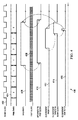
図2は、高速及び低速クロック速度の任意の比のための図1の中断処理回路100における動作信号を図示する信号図200を示す。この例において、第2のクロック信号SCLKの2つの例示的なサイクルがカーブ(curve)202として示され、FCLKカーブ204が、任意の数の高速クロック信号遷移を有し得、第1及び第2のクロック信号FCLK及びSCLKは、クロック速度及び位相関係に関して互いに対して完全に非同期とし得る。図2において分かるように、中断生成器回路110のフリップフロップ106は、第2のクロック信号SCLK(カーブ202)の立ち上がりエッジで第2の回路102からの中断要求信号IRの立ち上がりエッジに応答して、SET_FLAG信号(カーブ206)アクティブハイをアサートする。中断生成器回路110は、中断入力信号INT_INを生成し、同期化回路120はこの信号を同期化し、第2のクロック信号SCLKに対して非同期に2つのFCLKサイクル内で中断出力信号INT_OUT(カーブ210)において立ち上がりエッジを生成する。高速ドメインの第1の回路101が、関連する中断サービスルーチンを完了すると、第1の回路101はノード130において確認信号ACKをアサートし、これにより、中断クリアフリップフロップ116にアクティブハイデータ入力が提供される。第1のクロック信号FCLKの次の立ち上がりエッジで、フリップフロップ116は、クリアフラグ信号CLR_FLAG(アクティブハイ、図2のカーブ208)をアサートする。この信号遷移は、信号生成器フリップフロップ112をクリアし、中断入力信号INTをローに向かわせる。同期化回路120は、この立ち下がりエッジ遷移を2つの高速クロックサイクル内に同期化して、中断出力信号INT_OUTの立ち下がりエッジを引き起こす。このようにして、中断処理回路要素100は、確認信号ACKの2つのFCLKサイクル内に第1のクロック101に提供される中断信号INT_OUTを効果的にクリアする。
FIG. 2 shows a signal diagram 200 illustrating operating signals in the interrupt
図3は、高速及び低速クロック速度の1つの例示的な比(例えば、約8)について、図1の回路における動作信号を示す。この例において、低速ドメイン(第2の)回路102は、高速ドメインCPU又はプロセッサ第1回路101によるPWMタイマー周辺機器サービスである。この例において、高速ドメインCPUは、電力コンバータ信号(図示せず)のパルス幅を制御するため閉ループ制御応用例において、PWM制御周辺機器第2回路102にカウンタ値を提供する。周辺機器第2回路102は、カウント値をデクリメントし、カウント値が所定の値(例えば、本実装において「1」)に達すると、中断要求信号IRを発行する。図3におけるカーブ302は低速クロック信号SCLKを図示し、カーブ304は、PWMタイマー/カウンタデータ値を概略的に図示し、このケースでは、初期的に値3、2、1、0とデクリメントし、その後、高速クロックドメインCPUによって別の値2に再プログラムされる。その後、周辺機器パルス幅変調タイマー第2回路102は、この値2から1にデクリメントし、その後、再び0にデクリメントする。この例において、カーブ306は、フリップフロップ106からのSET_FLAG信号出力を図示し、カーブ308が、高速ドメインクロック信号FCLKを図示し、カーブ310が、同期化回路120からの中断出力信号INT_OUTを図示し、カーブ312が、フリップフロップ116からのCLEAR_FLAG信号を示す。この例において第2の回路102は、カウンタ値が「1」に達することに応答して中断要求信号をアサートする。図3において分かるように、中断出力信号INT_OUTは、SET_FLAG信号の立ち上がりエッジの2つの高速クロックサイクル内で立ち上がりエッジ遷移を受ける。中断出力信号に応答して、第1の回路101は、中断サービスルーチン又はプロセスを開始する。第1の回路101が中断サービスを完了すると、第1の回路101は確認信号ACKをアサートし、フリップフロップ116は、カーブ312として示されるCLEAR_FLAG信号において立ち上がりエッジを生成する。CLEAR_FLAG信号遷移は、中断生成器フリップフロップ112をクリアし、同期化回路120は、2つの高速クロックサイクル内で中断出力信号INT_OUT(カーブ310)において、結果として生じる立ち下がりエッジを生じさせる。
FIG. 3 shows the operating signals in the circuit of FIG. 1 for one exemplary ratio of high and low clock speeds (eg, about 8). In this example, the slow domain (second)
図2及び図3の例は、第2の回路102に関連する(例えば、2つの高速クロックサイクルにおける)中断事象の出現の第1の回路101の迅速な通知に関する中断処理回路100の有利なオペレーションを図示する。また、回路100は、第1の回路101による確認信号ACKのアサートに応答して、(例えば、2つの高速クロックサイクル内で)中断信号の高速非同期クリアを提供する。上述した中断処理回路要素101のこれらの迅速な応答利点は、図2及び図3に示すような著しい利点を提供する。また、これらの利点は、速いクロック速度と遅いクロック速度との間の比が増大される場合により顕著である。したがって、記載された回路及び手法の利点は、比較的遅いクロック速度の第2の回路102と相互作用する、高速CPU又は他の高速クロックドメイン回路要素に関連して特定の有用性を見出す。
The example of FIGS. 2 and 3 illustrates the advantageous operation of the interrupt
図4は、ミスした中断事象を備える、ハンドシェーキング確認中断処理手法を示す信号図400を提供する。図4におけるカーブ402は、例示的な低速クロック信号(図4においてLOW CLOCKと記される)を図示し、カーブ404が、PWMタイマー周辺機器におけるカウンタ又はタイマー値(PWM DATA)の別の例を図示し、カーブ406が、PWMタイマー周辺機器から高速クロックドメインプロセッサ回路への中断信号(INTERRUPT)を図示し、カーブ408が、例示的な高速クロック信号(FAST CLOCK)を示す。図4のカーブ410は、高速クロック信号に同期される中断信号を示し、カーブ412が、高速クロックドメイン回路からの例示的な中断クリア事象を示す。更なるカーブ414が、低速クロック信号に同期される中断クリア事象信号を図示し、カーブ416が、周辺機器回路から高速クロックドメイン回路への中断クリア事象確認ハンドシェーキング信号を図示する。図4の信号は、高速及び低速クロックドメイン回路要素間の従来のハンドシェーキング/確認ベースの中断処理の不利な結果を図示する。カーブ404及び406に見られるように、例えば、遅いドメイン回路102は、カウンタ値が「1」に達することに応答して中断信号IRを生成し、後続の高速ドメイン回路中断サービスルーチンは、遅いドメインPWMカウンタ値を「2」に再プログラムする。しかしながら、(カーブ412、414、及び416に示される)低速の第2のクロック信号への中断クリア事象の同期化は、中断シグナリング(カーブ414の立ち下がりエッジ)を実際に終了させるために信号(カーブ406の立ち下がりエッジ)を提供する際に著しい同期化遅延をもたらす。暫定遅延において、この例では、PWMカウンタ値は再度1に遷移しているが、高速クロックドメイン回路は、この第2の中断事象に応答して適切にサービスすることができない。図1〜図3に関連して上述したように、上述の中断処理回路要素100は、中断要求シグナリングの迅速な非同期クリアを有利に提供し、それによって、図4に図示された欠点を回避又は緩和するために高速クロックドメイン回路101による適切な中断サービス処理を助ける。
FIG. 4 provides a signal diagram 400 illustrating a handshaking confirmation suspend processing technique with a missed suspend event.
図5は、高速中断要求信号生成に関する中断処理回路要素100の利点を図示する信号図500を提供する。図5は、低速クロック信号SCLKを図示するカーブ502と、PWMのタイマー周辺機器カウンタ値を図示するカーブ504と、異なるレイテンシの生成された中断信号を図示するカーブ506、508、510とを含む。特に、カーブ506は、低速クロック信号サイクルの半分に対応するハーフサイクルレイテンシを有する中断信号(例えば、高速クロックドメインサービス回路に提供されるINTHL)を図示し、カーブ508は、フルの低速クロックサイクルレイテンシを有する中断信号のINTFLを図示する。対照的に、カーブ510は、上述した図1(INT_OUT)において中断生成器110及び同期化器120によって提供される高速中断生成を示す。前述のように、以前の解決策は同期化回路要素(図示せず)を用いて、ハーフサイクル遅延(たとえば、カーブ506)又はフル低速クロックサイクル遅延(カーブ508)を導入する、低速クロック回路要素における中断事象に関連するシグナリングを同期させる。対照的に、上述の回路100は、低速クロックドメイン同期化器を用いず、中断要求信号SET_FLAGを、非同期ロジックが完全に含まれるように信号INT_OUTとして高速クロックドメインに同期された後、中断要求ラインとして搬送する。この点に関し、ノード111上のSET_FLAG信号は、中断入力信号INT_INを生成するフリップフロップ112へのクロックとして用いられ、回路要素110、120は、低速クロックドメインにおいていかなる不利益もなしに中断出力信号INT_OUTを生成する。
FIG. 5 provides a signal diagram 500 illustrating the benefits of the interrupt handling
図6は、第1のクロック信号より遅い第2のクロック信号に従って動作される第2の回路(例えば、回路102)によって第1のクロック信号に従って動作される第1の回路(例えば、上述の回路101)の中断を管理する方法600を示す。方法600は、上述の回路100など、又は他の回路要素(図示せず)における、任意の好適な中断処理回路要素を用いて実装され得る。602において、第2のクロック信号に同期される中断信号が生成される。一例において、上述の低速クロックドメイン回路102は、フリップフロップ106を介してSCLK信号に同期されるSET_FLAG信号を中断生成器フリップフロップ112に提供する。これは、遅いクロックドメインレイテンシを伴わずに、602において中断入力信号INT_INを生成する(例えば、上述の図5のカーブ506及び508に示される遅延を回避する)。
FIG. 6 illustrates a first circuit (eg, the circuit described above) operated according to a first clock signal by a second circuit (eg, circuit 102) operated according to a second clock signal that is slower than the first clock signal. 101 shows a
604及び606において、中断出力信号が、中断入力信号に応答して第1の回路101に提供される。上述した例では、図6における604において、中断生成器フリップフロップ112が中断入力信号INT_INを同期化回路120に提供し、同期化回路120は、高速クロック信号FCLKに同期して、606において中断出力信号INT_OUTを第1の回路101に提供する。608において、第1の回路は、高速クロック信号FCLKに同期される確認信号(例えば、上述のACK)を提供する。方法600は、610において中断入力及び出力信号をクリアすることを更に含む。いくつかの例において、INT_IN及びINT_OUT信号は、確認信号ACKに応答して、クリア回路要素114、116によって第2のクロック信号SCLKに対して非同期にクリアされる。回路100において、中断入力及び出力信号INT_IN及びINT_OUTは、クリアフリップフロップ116が確認信号ACKを受信した後、第1のクロック信号FCLKの2サイクル内に迅速にクリアされる。
At 604 and 606, an interrupt output signal is provided to the
記載される例は、高速クロックドメインにおいて生成されるクリア事象信号の低速クロックドメイン同期化を用いる他の解決策に比して著しい応答時間利点を提供する。図4に示すように、そのような代替解決策は、高速クロックドメイン回路要素に提供される中断信号を実際にクリアする前に、同期化のために2つの追加の低速クロックサイクルを消費する。これに対し、記載された回路要素100及び方法600は、低速クロック信号SCLKに非同期的に低速クロックドメインにおいて生成された中断をクリアすることによって、そのような追加の中断クリアレイテンシ又は遅延を回避する。例えば、回路100において、高速クロックドメイン回路101からのクリア事象信号ACKを非同期的に用いて、中断入力信号INT_INを生成する同じフリップフロップ112をクリアして、低速クロックドメインにおける何の不利益もなく、中断出力信号INT_OUTを確実にクリアする。中断生成のため、説明された回路及び方法は、同期化回路120を用いて高速クロック信号FCLKに対して同期して中断出力信号INT_OUTを搬送して、クリアなシグナリングを保証し、如何なる非同期経路(例えば、準安定性)も回避する。この同期化は実際には、特に第1のクロック速度が低速クロック速度より著しく高い場合に、小さな遅延である。また、記載された回路100は、高速クロックドメインに完全に同期されるように最終的な中断ラインを依然として維持しながら、高速非同期クリア経路を実装する。
The described example offers significant response time advantages over other solutions using slow clock domain synchronization of the clear event signal generated in the fast clock domain. As shown in FIG. 4, such an alternative solution consumes two additional slow clock cycles for synchronization before actually clearing the suspend signal provided to the fast clock domain circuitry. In contrast, the described
本発明の特許請求の範囲内で、説明した例示の実施例に改変が成され得、他の実施例が可能である。 Modifications may be made to the exemplary embodiments described within the scope of the claims of the present invention, and other embodiments are possible.
Claims (20)
中断処理回路であって、中断要求信号を受信するための第1の中断生成器入力と、中断クリア信号を受信するための第2の中断生成器入力と、前記第1の回路を選択的に中断するために前記中断要求信号に同期される中断入力信号を提供するための中断生成器出力とを含む、前記中断生成器回路、及び
前記第1の回路からの確認信号に応答して前記中断生成器回路をリセットするため前記中断クリア信号を選択的に提供するために前記第1のクロック信号に同期される出力を含む中断クリア回路、
を含む、中断処理回路。 An interruption processing circuit that manages interruption of the first circuit operated according to the first clock signal by a second circuit operated according to a second clock signal that is slower than the first clock signal,
An interrupt processing circuit, wherein a first interrupt generator input for receiving an interrupt request signal, a second interrupt generator input for receiving an interrupt clear signal, and selectively interrupting the first circuit. An interrupt generator output for providing an interrupt input signal synchronized with the interrupt request signal to interrupt, the interrupt generator circuit; and the interrupt in response to a confirmation signal from the first circuit. An interrupt clear circuit including an output synchronized with the first clock signal to selectively provide the interrupt clear signal for resetting a generator circuit;
And an interruption processing circuit.
前記中断要求信号が、前記第2の回路によって中断が要求されていないことを示す第1の状態と、前記第2の回路によって中断が要求されていることを示す異なる第2の状態とを有し、
前記中断クリア信号が、第1の状態と、異なる第2の状態とを有し、
前記中断生成器出力が、第1の状態の前記中断クリア信号を受信する前記第2の中断生成器入力に応答して前記第1の状態の前記中断入力信号を提供するように、及び、前記中断クリア信号が第2の状態にあるとき前記第1の状態から前記第2の状態に遷移する前記中断要求信号に応答して異なる第2の状態の中断入力信号を提供するように構成され、
前記中断クリア回路が、前記第1の回路からの前記確認信号に応答して前記中断入力信号を前記第1の状態に設定するために前記中断生成器回路をリセットするために、前記第1の状態の前記中断クリア信号を選択的に提供するように構成される、
中断処理回路。 The interruption processing circuit according to claim 1, wherein
The interruption request signal has a first state indicating that interruption is not requested by the second circuit and a different second state indicating that interruption is requested by the second circuit. And
The interrupt clear signal has a first state and a different second state;
The interrupt generator output provides the interrupt input signal in the first state in response to the second interrupt generator input receiving the interrupt clear signal in a first state; and Configured to provide a different second state interrupt input signal in response to the interrupt request signal transitioning from the first state to the second state when the interrupt clear signal is in the second state;
The first interrupt circuit for resetting the interrupt generator circuit to set the interrupt input signal to the first state in response to the confirmation signal from the first circuit; Configured to selectively provide the interrupt clear signal of a state;
Interrupt processing circuit.
前記同期化回路が、前記中断入力信号を受信するために前記中断生成器出力に結合される入力と、前記第1の回路に中断出力信号を提供するために前記第1のクロック信号に同期される出力とを含む、
中断処理回路。 The interruption processing circuit according to claim 2, further comprising a synchronization circuit,
The synchronization circuit is synchronized with an input coupled to the interrupt generator output to receive the interrupt input signal, and with the first clock signal to provide an interrupt output signal to the first circuit. Output including
Interrupt processing circuit.
前記中断生成器出力に接続されるデータ入力と、前記第1のクロック信号を受信するために前記第1の回路に接続されるクロック入力と、出力とを含む第1のフリップフロップ、及び
第2のフリップフロップであって、前記第1のフリップフロップの前記出力に接続されるデータ入力と、前記第1のクロック信号を受信するため前記第1の回路に接続されるクロック入力と、前記第1の回路に同期される前記中断出力信号を提供するため前記第1の回路に接続される出力とを含む、前記第2のフリップフロップ、
を含む、中断処理回路。 The interruption processing circuit according to claim 3, wherein the synchronization circuit comprises:
A first flip-flop including a data input connected to the interrupt generator output, a clock input connected to the first circuit for receiving the first clock signal, and an output; A flip-flop comprising: a data input connected to the output of the first flip-flop; a clock input connected to the first circuit for receiving the first clock signal; An output connected to the first circuit to provide the interrupted output signal synchronized to the circuit of the second flip-flop.
And an interruption processing circuit.
前記中断生成器回路が第3のフリップフロップを含み、前記第3のフリップフロップが、基準電圧に接続されるデータ入力と、前記中断要求信号を受信するために接続されるクロック入力と、前記中断クリア信号を受信するため前記中断クリア回路の前記出力に接続されるクリア入力と、前記中断入力信号を前記第1のフリップフロップの前記データ入力に提供するため前記中断生成器出力に接続される出力とを含む、
中断処理回路。 The interruption processing circuit according to claim 4, wherein
The interrupt generator circuit includes a third flip-flop, wherein the third flip-flop has a data input connected to a reference voltage; a clock input connected to receive the interrupt request signal; A clear input connected to the output of the interrupt clear circuit for receiving a clear signal; and an output connected to the interrupt generator output for providing the interrupt input signal to the data input of the first flip-flop. Including
Interrupt processing circuit.
前記中断生成器回路がフリップフロップを含み、前記フリップフロップが、基準電圧に接続されるデータ入力と、前記中断要求信号を受信するために接続されるクロック入力と、前記中断クリア信号を受信するため前記中断クリア回路の前記出力に接続されるクリア入力と、前記中断入力信号を前記同期化回路の前記入力に提供するため前記中断生成器出力に接続される出力とを含む、
中断処理回路。 The interruption processing circuit according to claim 3, wherein
The interrupt generator circuit includes a flip-flop, the flip-flop receiving a data input connected to a reference voltage, a clock input connected to receive the interrupt request signal, and receiving the interrupt clear signal. A clear input connected to the output of the interrupt clear circuit, and an output connected to the interrupt generator output to provide the interrupt input signal to the input of the synchronization circuit.
Interrupt processing circuit.
前記中断生成器回路がフリップフロップを含み、前記フリップフロップが、基準電圧に接続されるデータ入力と、前記中断要求信号を受信するために接続されるクロック入力と、前記中断クリア信号を受信するために前記中断クリア回路の前記出力に接続されるクリア入力と、前記中断入力信号を提供するため前記中断生成器出力に接続される出力とを含む、
中断処理回路。 The interruption processing circuit according to claim 2,
The interrupt generator circuit includes a flip-flop, the flip-flop receiving a data input connected to a reference voltage, a clock input connected to receive the interrupt request signal, and receiving the interrupt clear signal. A clear input connected to the output of the interrupt clear circuit, and an output connected to the interrupt generator output to provide the interrupt input signal.
Interrupt processing circuit.
第2のフリップフロップを更に含み、前記第2のフリップフロップが、前記中断要求信号を受信するために前記第2の回路に接続されるデータ入力と、前記第2のクロック信号を受信するために接続されるクロック入力と、前記第2のクロック信号に同期される同期された中断要求信号を提供するための出力とを含む、
中断処理回路。 The interruption processing circuit according to claim 7, wherein
And a second flip-flop for receiving the second clock signal and a data input connected to the second circuit for receiving the interrupt request signal. A clock input connected thereto, and an output for providing a synchronized interrupt request signal synchronized to the second clock signal.
Interrupt processing circuit.
前記第1のクロック信号に対して同期して前記第1の回路を選択的に中断するための中断生成器回路、及び
前記第2のクロック信号に対して非同期に前記第1の回路からの確認信号に応答して前記生成器回路を選択的にリセットするための出力を含む中断クリア回路、
を含む、中断処理回路。 An interruption processing circuit that manages interruption of the first circuit operated according to the first clock signal by a second circuit operated according to a second clock signal that is slower than the first clock signal, wherein the interruption is performed. The processing circuit is
An interrupt generator circuit for selectively interrupting the first circuit in synchronization with the first clock signal; and confirmation from the first circuit asynchronously with respect to the second clock signal. An interrupt clear circuit including an output for selectively resetting the generator circuit in response to a signal.
And an interruption processing circuit.
前記中断生成器回路の出力に接続されるデータ入力と、前記第1のクロック信号を受信するために前記第1の回路に接続されるクロック入力と、出力とを含む第1のフリップフロップ、及び
前記第1のフリップフロップの前記出力に接続されるデータ入力と、前記第1のクロック信号を受信するために前記第1の回路に接続されるクロック入力と、前記第1のクロック信号に同期される前記中断出力信号を提供するために前記第1の回路に接続される出力とを含む第2のフリップフロップ、
を含む、中断処理回路。 The interruption processing circuit according to claim 11, wherein the synchronization circuit comprises:
A first flip-flop including a data input connected to an output of the interrupt generator circuit, a clock input connected to the first circuit for receiving the first clock signal, and an output; A data input connected to the output of the first flip-flop; a clock input connected to the first circuit for receiving the first clock signal; and a clock input connected to the first circuit. An output connected to the first circuit to provide the interrupted output signal.
And an interruption processing circuit.
前記第3のフリップフロップが、基準電圧に接続されるデータ入力と、中断要求信号を受信するために前記第1の回路に接続されるクロック入力と、前記中断クリア回路から中断クリア信号を受信するために接続されるクリア入力と、前記中断生成器回路をリセットするための中断入力信号を選択的に提供するための出力とを含む、
中断処理信号。 13. The interruption processing circuit according to claim 12, wherein the interruption generator circuit includes a third flip-flop.
The third flip-flop receives a data input connected to a reference voltage, a clock input connected to the first circuit for receiving an interrupt request signal, and an interrupt clear signal from the interrupt clear circuit. And an output for selectively providing an interrupt input signal for resetting the interrupt generator circuit.
Interrupt processing signal.
前記フリップフロップが、前記第2の回路から中断要求信号を受信するためのデータ入力と、前記第2のクロック信号を受信するために接続されるクロック入力と、前記第1の回路を選択的に中断するため、前記第2のクロック信号に同期される同期された中断要求信号を前記中断生成器回路に提供するための出力とを含む、
中断処理生成器回路。 The interrupt processing circuit according to claim 10, further comprising a flip-flop,
The flip-flop selectively connects a data input for receiving an interrupt request signal from the second circuit, a clock input connected to receive the second clock signal, and the first circuit. An output for providing a synchronized interrupt request signal to the interrupt generator circuit for interrupting, the interrupt request signal being synchronized with the second clock signal.
Interrupt processing generator circuit.
前記第2のクロック信号に同期される中断入力信号を生成すること、
前記中断入力信号に応答して前記第1の回路に中断出力信号を提供すること、及び
前記第1の回路からの確認信号に応答して前記第2のクロック信号に対して非同期に前記中断入力及び出力信号をクリアすること、
を含む、方法。 A method for managing interruption of a first circuit operated according to a first clock signal by a second circuit operated according to a second clock signal that is slower than the first clock signal, the method comprising:
Generating an interrupt input signal that is synchronized with the second clock signal;
Providing an interrupt output signal to the first circuit in response to the interrupt input signal; and providing the interrupt input asynchronously with respect to the second clock signal in response to an acknowledgment signal from the first circuit. And clearing the output signal,
Including, methods.
前記第2の回路から中断要求信号を受信すること、
前記中断要求信号に応答して前記中断入力信号を生成すること、及び
前記第2のクロック信号に対して非同期に前記中断入力信号に応答して前記第1の回路に前記中断出力信号を提供すること、
を更に含む、方法。 17. The method according to claim 16, wherein
Receiving an interrupt request signal from the second circuit;
Generating the interrupt input signal in response to the interrupt request signal; and providing the interrupt output signal to the first circuit in response to the interrupt input signal asynchronously with respect to the second clock signal. thing,
The method further comprising:
Applications Claiming Priority (3)
| Application Number | Priority Date | Filing Date | Title |
|---|---|---|---|
| US15/420,267 | 2017-01-31 | ||
| US15/420,267 US10788853B2 (en) | 2017-01-31 | 2017-01-31 | Interrupt handling method and apparatus for slow peripherals |
| PCT/US2018/016206 WO2018144583A1 (en) | 2017-01-31 | 2018-01-31 | Interrupt handling method and apparatus for slow peripherals |
Publications (2)
| Publication Number | Publication Date |
|---|---|
| JP2020507176A true JP2020507176A (en) | 2020-03-05 |
| JP2020507176A5 JP2020507176A5 (en) | 2021-03-11 |
Family
ID=62979832
Family Applications (1)
| Application Number | Title | Priority Date | Filing Date |
|---|---|---|---|
| JP2019562234A Pending JP2020507176A (en) | 2017-01-31 | 2018-01-31 | Interruption processing method and apparatus for low-speed peripheral devices |
Country Status (5)
| Country | Link |
|---|---|
| US (2) | US10788853B2 (en) |
| EP (1) | EP3577557A4 (en) |
| JP (1) | JP2020507176A (en) |
| CN (1) | CN110249309A (en) |
| WO (1) | WO2018144583A1 (en) |
Families Citing this family (3)
| Publication number | Priority date | Publication date | Assignee | Title |
|---|---|---|---|---|
| FR3109227B1 (en) | 2020-04-14 | 2022-05-06 | St Microelectronics Alps Sas | Interrupt controller and method for managing such a controller |
| CN113885654A (en) * | 2020-07-03 | 2022-01-04 | 富泰华工业(深圳)有限公司 | Cross-clock-domain signal transmission method, circuit and electronic device |
| US11200184B1 (en) * | 2020-12-22 | 2021-12-14 | Industrial Technology Research Institute | Interrupt control device and interrupt control method between clock domains |
Citations (3)
| Publication number | Priority date | Publication date | Assignee | Title |
|---|---|---|---|---|
| JP2001184298A (en) * | 1999-12-27 | 2001-07-06 | Toshiba Corp | Circuit and method for reporting asynchronous interruption |
| JP2002149419A (en) * | 2000-11-03 | 2002-05-24 | Arm Ltd | Logic unit for clarifying interruption and integrated circuit |
| JP2009282780A (en) * | 2008-05-22 | 2009-12-03 | Atmel Germany Gmbh | Formation device of receipt signal |
Family Cites Families (14)
| Publication number | Priority date | Publication date | Assignee | Title |
|---|---|---|---|---|
| KR920003152A (en) | 1990-07-31 | 1992-02-29 | 이헌조 | Multi Interrupt Processing Circuit |
| US5900753A (en) * | 1997-03-28 | 1999-05-04 | Logicvision, Inc. | Asynchronous interface |
| US6507609B1 (en) | 1999-01-20 | 2003-01-14 | Advanced Micro Devices, Inc. | Mechanism for capturing and reporting interrupt events of different clock domains |
| JP2002041452A (en) | 2000-07-27 | 2002-02-08 | Hitachi Ltd | Microprocessor, semiconductor module and data processing system |
| US6823413B2 (en) | 2001-06-08 | 2004-11-23 | Oki Electronic Industry Co., Ltd. | Interrupt signal processing apparatus |
| ATE510373T1 (en) * | 2003-06-25 | 2011-06-15 | Nxp Bv | LOSSLESS TRANSFER OF EVENTS ACROSS CLOCK DOMAIN |
| US20060064529A1 (en) | 2004-09-23 | 2006-03-23 | International Business Machines Corporation | Method and system for controlling peripheral adapter interrupt frequency by transferring processor load information to the peripheral adapter |
| DE102007023442B3 (en) * | 2007-05-19 | 2008-10-09 | Atmel Germany Gmbh | Device and method for generating an acknowledgment signal |
| US7934113B2 (en) | 2007-05-21 | 2011-04-26 | Texas Instruments Incorporated | Self-clearing asynchronous interrupt edge detect latching register |
| WO2011114438A1 (en) * | 2010-03-16 | 2011-09-22 | 三菱電機株式会社 | Speed detection device |
| CN103631649B (en) * | 2012-08-24 | 2018-08-28 | 深圳市中兴微电子技术有限公司 | Interruption processing method, device and interrupt control unit |
| US10014041B1 (en) * | 2016-12-23 | 2018-07-03 | Texas Instruments Incorporated | Integrated circuits, methods and interface circuitry to synchronize data transfer between high and low speed clock domains |
| CN113885654A (en) * | 2020-07-03 | 2022-01-04 | 富泰华工业(深圳)有限公司 | Cross-clock-domain signal transmission method, circuit and electronic device |
| US11200184B1 (en) * | 2020-12-22 | 2021-12-14 | Industrial Technology Research Institute | Interrupt control device and interrupt control method between clock domains |
-
2017
- 2017-01-31 US US15/420,267 patent/US10788853B2/en active Active
-
2018
- 2018-01-31 CN CN201880009131.2A patent/CN110249309A/en active Pending
- 2018-01-31 WO PCT/US2018/016206 patent/WO2018144583A1/en unknown
- 2018-01-31 JP JP2019562234A patent/JP2020507176A/en active Pending
- 2018-01-31 EP EP18747681.7A patent/EP3577557A4/en not_active Withdrawn
-
2020
- 2020-08-18 US US16/995,852 patent/US20200379505A1/en active Pending
Patent Citations (3)
| Publication number | Priority date | Publication date | Assignee | Title |
|---|---|---|---|---|
| JP2001184298A (en) * | 1999-12-27 | 2001-07-06 | Toshiba Corp | Circuit and method for reporting asynchronous interruption |
| JP2002149419A (en) * | 2000-11-03 | 2002-05-24 | Arm Ltd | Logic unit for clarifying interruption and integrated circuit |
| JP2009282780A (en) * | 2008-05-22 | 2009-12-03 | Atmel Germany Gmbh | Formation device of receipt signal |
Also Published As
| Publication number | Publication date |
|---|---|
| EP3577557A1 (en) | 2019-12-11 |
| US20200379505A1 (en) | 2020-12-03 |
| US20180217630A1 (en) | 2018-08-02 |
| US10788853B2 (en) | 2020-09-29 |
| EP3577557A4 (en) | 2020-06-03 |
| WO2018144583A1 (en) | 2018-08-09 |
| CN110249309A (en) | 2019-09-17 |
Similar Documents
| Publication | Publication Date | Title |
|---|---|---|
| US20200379505A1 (en) | Interrupt handling method and apparatus for slow peripherals | |
| US10014041B1 (en) | Integrated circuits, methods and interface circuitry to synchronize data transfer between high and low speed clock domains | |
| US8977882B2 (en) | System for data transfer between asynchronous clock domains | |
| US8570069B2 (en) | Clock gating cell circuit | |
| TWI488437B (en) | Integrated circuit device, synchronisation module, electronic device and method therefor | |
| TWI727075B (en) | Semiconductor device | |
| US8132036B2 (en) | Reducing latency in data transfer between asynchronous clock domains | |
| GB2513529A (en) | System and method of low latency data tranfer between clock domains operated in various synchronization modes | |
| US7500132B1 (en) | Method of asynchronously transmitting data between clock domains | |
| JP2001077797A (en) | Interface device | |
| US20100315134A1 (en) | Systems and methods for multi-lane communication busses | |
| TWI757033B (en) | Interrupt control device and interrupt control method between clock domains | |
| CN108694146B (en) | Asynchronous/synchronous interface circuit | |
| US8176352B2 (en) | Clock domain data transfer device and methods thereof | |
| US7123674B2 (en) | Reducing latency and power in asynchronous data transfers | |
| WO2022037638A1 (en) | Integrated circuit reset method and integrated circuit | |
| JP2002149419A (en) | Logic unit for clarifying interruption and integrated circuit | |
| JP3604637B2 (en) | Asynchronous transfer device and asynchronous transfer method | |
| US20110018585A1 (en) | Methods, systems and arrangements for edge detection | |
| US10429881B2 (en) | Semiconductor device for stopping an oscillating clock signal from being provided to an IP block, a semiconductor system having the semiconductor device, and a method of operating the semiconductor device | |
| EP3739463B1 (en) | Circuit for asynchronous data transfer | |
| JP2006201856A (en) | Semiconductor integrated circuit | |
| JP5315882B2 (en) | Semiconductor device and communication method | |
| KR102568225B1 (en) | Semiconductor device, semiconductor system and method for operating semiconductor device | |
| JP5413367B2 (en) | Semiconductor device and communication method |
Legal Events
| Date | Code | Title | Description |
|---|---|---|---|
| A521 | Request for written amendment filed |
Free format text: JAPANESE INTERMEDIATE CODE: A821 Effective date: 20190731 |
|
| A521 | Request for written amendment filed |
Free format text: JAPANESE INTERMEDIATE CODE: A523 Effective date: 20210127 |
|
| A621 | Written request for application examination |
Free format text: JAPANESE INTERMEDIATE CODE: A621 Effective date: 20210127 |
|
| A711 | Notification of change in applicant |
Free format text: JAPANESE INTERMEDIATE CODE: A711 Effective date: 20210218 |
|
| A521 | Request for written amendment filed |
Free format text: JAPANESE INTERMEDIATE CODE: A523 Effective date: 20210323 |
|
| A521 | Request for written amendment filed |
Free format text: JAPANESE INTERMEDIATE CODE: A523 Effective date: 20210602 |
|
| A977 | Report on retrieval |
Free format text: JAPANESE INTERMEDIATE CODE: A971007 Effective date: 20210813 |
|
| A131 | Notification of reasons for refusal |
Free format text: JAPANESE INTERMEDIATE CODE: A131 Effective date: 20210825 |
|
| A601 | Written request for extension of time |
Free format text: JAPANESE INTERMEDIATE CODE: A601 Effective date: 20211124 |
|
| A601 | Written request for extension of time |
Free format text: JAPANESE INTERMEDIATE CODE: A601 Effective date: 20220120 |
|
| A02 | Decision of refusal |
Free format text: JAPANESE INTERMEDIATE CODE: A02 Effective date: 20220427 |