JP2020184870A - High frequency generator and how it works - Google Patents
High frequency generator and how it works Download PDFInfo
- Publication number
- JP2020184870A JP2020184870A JP2019110832A JP2019110832A JP2020184870A JP 2020184870 A JP2020184870 A JP 2020184870A JP 2019110832 A JP2019110832 A JP 2019110832A JP 2019110832 A JP2019110832 A JP 2019110832A JP 2020184870 A JP2020184870 A JP 2020184870A
- Authority
- JP
- Japan
- Prior art keywords
- frequency
- ignition
- voltage
- load
- signal
- Prior art date
- Legal status (The legal status is an assumption and is not a legal conclusion. Google has not performed a legal analysis and makes no representation as to the accuracy of the status listed.)
- Granted
Links
Images
Classifications
-
- H—ELECTRICITY
- H01—ELECTRIC ELEMENTS
- H01J—ELECTRIC DISCHARGE TUBES OR DISCHARGE LAMPS
- H01J37/00—Discharge tubes with provision for introducing objects or material to be exposed to the discharge, e.g. for the purpose of examination or processing thereof
- H01J37/32—Gas-filled discharge tubes
- H01J37/32009—Arrangements for generation of plasma specially adapted for examination or treatment of objects, e.g. plasma sources
- H01J37/32082—Radio frequency generated discharge
- H01J37/32137—Radio frequency generated discharge controlling of the discharge by modulation of energy
- H01J37/32146—Amplitude modulation, includes pulsing
-
- H—ELECTRICITY
- H02—GENERATION; CONVERSION OR DISTRIBUTION OF ELECTRIC POWER
- H02M—APPARATUS FOR CONVERSION BETWEEN AC AND AC, BETWEEN AC AND DC, OR BETWEEN DC AND DC, AND FOR USE WITH MAINS OR SIMILAR POWER SUPPLY SYSTEMS; CONVERSION OF DC OR AC INPUT POWER INTO SURGE OUTPUT POWER; CONTROL OR REGULATION THEREOF
- H02M3/00—Conversion of DC power input into DC power output
- H02M3/22—Conversion of DC power input into DC power output with intermediate conversion into AC
- H02M3/24—Conversion of DC power input into DC power output with intermediate conversion into AC by static converters
- H02M3/28—Conversion of DC power input into DC power output with intermediate conversion into AC by static converters using discharge tubes with control electrode or semiconductor devices with control electrode to produce the intermediate AC
- H02M3/325—Conversion of DC power input into DC power output with intermediate conversion into AC by static converters using discharge tubes with control electrode or semiconductor devices with control electrode to produce the intermediate AC using devices of a triode or a transistor type requiring continuous application of a control signal
- H02M3/335—Conversion of DC power input into DC power output with intermediate conversion into AC by static converters using discharge tubes with control electrode or semiconductor devices with control electrode to produce the intermediate AC using devices of a triode or a transistor type requiring continuous application of a control signal using semiconductor devices only
-
- H—ELECTRICITY
- H01—ELECTRIC ELEMENTS
- H01J—ELECTRIC DISCHARGE TUBES OR DISCHARGE LAMPS
- H01J37/00—Discharge tubes with provision for introducing objects or material to be exposed to the discharge, e.g. for the purpose of examination or processing thereof
- H01J37/32—Gas-filled discharge tubes
- H01J37/32009—Arrangements for generation of plasma specially adapted for examination or treatment of objects, e.g. plasma sources
- H01J37/32082—Radio frequency generated discharge
- H01J37/32174—Circuits specially adapted for controlling the RF discharge
-
- H—ELECTRICITY
- H02—GENERATION; CONVERSION OR DISTRIBUTION OF ELECTRIC POWER
- H02M—APPARATUS FOR CONVERSION BETWEEN AC AND AC, BETWEEN AC AND DC, OR BETWEEN DC AND DC, AND FOR USE WITH MAINS OR SIMILAR POWER SUPPLY SYSTEMS; CONVERSION OF DC OR AC INPUT POWER INTO SURGE OUTPUT POWER; CONTROL OR REGULATION THEREOF
- H02M1/00—Details of apparatus for conversion
- H02M1/0064—Magnetic structures combining different functions, e.g. storage, filtering or transformation
-
- H—ELECTRICITY
- H02—GENERATION; CONVERSION OR DISTRIBUTION OF ELECTRIC POWER
- H02M—APPARATUS FOR CONVERSION BETWEEN AC AND AC, BETWEEN AC AND DC, OR BETWEEN DC AND DC, AND FOR USE WITH MAINS OR SIMILAR POWER SUPPLY SYSTEMS; CONVERSION OF DC OR AC INPUT POWER INTO SURGE OUTPUT POWER; CONTROL OR REGULATION THEREOF
- H02M1/00—Details of apparatus for conversion
- H02M1/08—Circuits specially adapted for the generation of control voltages for semiconductor devices incorporated in static converters
-
- H—ELECTRICITY
- H02—GENERATION; CONVERSION OR DISTRIBUTION OF ELECTRIC POWER
- H02M—APPARATUS FOR CONVERSION BETWEEN AC AND AC, BETWEEN AC AND DC, OR BETWEEN DC AND DC, AND FOR USE WITH MAINS OR SIMILAR POWER SUPPLY SYSTEMS; CONVERSION OF DC OR AC INPUT POWER INTO SURGE OUTPUT POWER; CONTROL OR REGULATION THEREOF
- H02M1/00—Details of apparatus for conversion
- H02M1/32—Means for protecting converters other than automatic disconnection
-
- H—ELECTRICITY
- H02—GENERATION; CONVERSION OR DISTRIBUTION OF ELECTRIC POWER
- H02M—APPARATUS FOR CONVERSION BETWEEN AC AND AC, BETWEEN AC AND DC, OR BETWEEN DC AND DC, AND FOR USE WITH MAINS OR SIMILAR POWER SUPPLY SYSTEMS; CONVERSION OF DC OR AC INPUT POWER INTO SURGE OUTPUT POWER; CONTROL OR REGULATION THEREOF
- H02M7/00—Conversion of AC power input into DC power output; Conversion of DC power input into AC power output
- H02M7/42—Conversion of DC power input into AC power output without possibility of reversal
- H02M7/44—Conversion of DC power input into AC power output without possibility of reversal by static converters
- H02M7/48—Conversion of DC power input into AC power output without possibility of reversal by static converters using discharge tubes with control electrode or semiconductor devices with control electrode
- H02M7/53—Conversion of DC power input into AC power output without possibility of reversal by static converters using discharge tubes with control electrode or semiconductor devices with control electrode using devices of a triode or transistor type requiring continuous application of a control signal
- H02M7/537—Conversion of DC power input into AC power output without possibility of reversal by static converters using discharge tubes with control electrode or semiconductor devices with control electrode using devices of a triode or transistor type requiring continuous application of a control signal using semiconductor devices only, e.g. single switched pulse inverters
- H02M7/539—Conversion of DC power input into AC power output without possibility of reversal by static converters using discharge tubes with control electrode or semiconductor devices with control electrode using devices of a triode or transistor type requiring continuous application of a control signal using semiconductor devices only, e.g. single switched pulse inverters with automatic control of output wave form or frequency
- H02M7/5395—Conversion of DC power input into AC power output without possibility of reversal by static converters using discharge tubes with control electrode or semiconductor devices with control electrode using devices of a triode or transistor type requiring continuous application of a control signal using semiconductor devices only, e.g. single switched pulse inverters with automatic control of output wave form or frequency by pulse-width modulation
-
- H—ELECTRICITY
- H02—GENERATION; CONVERSION OR DISTRIBUTION OF ELECTRIC POWER
- H02M—APPARATUS FOR CONVERSION BETWEEN AC AND AC, BETWEEN AC AND DC, OR BETWEEN DC AND DC, AND FOR USE WITH MAINS OR SIMILAR POWER SUPPLY SYSTEMS; CONVERSION OF DC OR AC INPUT POWER INTO SURGE OUTPUT POWER; CONTROL OR REGULATION THEREOF
- H02M1/00—Details of apparatus for conversion
- H02M1/0067—Converter structures employing plural converter units, other than for parallel operation of the units on a single load
- H02M1/007—Plural converter units in cascade
-
- H—ELECTRICITY
- H02—GENERATION; CONVERSION OR DISTRIBUTION OF ELECTRIC POWER
- H02M—APPARATUS FOR CONVERSION BETWEEN AC AND AC, BETWEEN AC AND DC, OR BETWEEN DC AND DC, AND FOR USE WITH MAINS OR SIMILAR POWER SUPPLY SYSTEMS; CONVERSION OF DC OR AC INPUT POWER INTO SURGE OUTPUT POWER; CONTROL OR REGULATION THEREOF
- H02M1/00—Details of apparatus for conversion
- H02M1/44—Circuits or arrangements for compensating for electromagnetic interference in converters or inverters
-
- H—ELECTRICITY
- H02—GENERATION; CONVERSION OR DISTRIBUTION OF ELECTRIC POWER
- H02M—APPARATUS FOR CONVERSION BETWEEN AC AND AC, BETWEEN AC AND DC, OR BETWEEN DC AND DC, AND FOR USE WITH MAINS OR SIMILAR POWER SUPPLY SYSTEMS; CONVERSION OF DC OR AC INPUT POWER INTO SURGE OUTPUT POWER; CONTROL OR REGULATION THEREOF
- H02M7/00—Conversion of AC power input into DC power output; Conversion of DC power input into AC power output
- H02M7/42—Conversion of DC power input into AC power output without possibility of reversal
- H02M7/44—Conversion of DC power input into AC power output without possibility of reversal by static converters
- H02M7/48—Conversion of DC power input into AC power output without possibility of reversal by static converters using discharge tubes with control electrode or semiconductor devices with control electrode
- H02M7/4815—Resonant converters
-
- Y—GENERAL TAGGING OF NEW TECHNOLOGICAL DEVELOPMENTS; GENERAL TAGGING OF CROSS-SECTIONAL TECHNOLOGIES SPANNING OVER SEVERAL SECTIONS OF THE IPC; TECHNICAL SUBJECTS COVERED BY FORMER USPC CROSS-REFERENCE ART COLLECTIONS [XRACs] AND DIGESTS
- Y02—TECHNOLOGIES OR APPLICATIONS FOR MITIGATION OR ADAPTATION AGAINST CLIMATE CHANGE
- Y02B—CLIMATE CHANGE MITIGATION TECHNOLOGIES RELATED TO BUILDINGS, e.g. HOUSING, HOUSE APPLIANCES OR RELATED END-USER APPLICATIONS
- Y02B70/00—Technologies for an efficient end-user side electric power management and consumption
- Y02B70/10—Technologies improving the efficiency by using switched-mode power supplies [SMPS], i.e. efficient power electronics conversion e.g. power factor correction or reduction of losses in power supplies or efficient standby modes
Landscapes
- Engineering & Computer Science (AREA)
- Power Engineering (AREA)
- Physics & Mathematics (AREA)
- Plasma & Fusion (AREA)
- Chemical & Material Sciences (AREA)
- Analytical Chemistry (AREA)
- Inverter Devices (AREA)
Abstract
【課題】出力電流の過渡現象を防止できる高周波ジェネレータおよびその動作方法を提供する。【解決手段】本発明の高周波ジェネレータは、交互に動作する第1及び第2スイッチング素子を含み、DC/DCコンバータから出力される直流電圧を交流電圧に変換するインバータと、そこから出力される高周波信号から共振周波数を有するサイン波形の共振信号を出力するLCフィルタと、そこから出力されるパルス波形の高周波電力信号を2次側に誘導するトランスフォーマと、イグニッションモード終了時のスイッチング周波数をイグニッションモード離脱周波数にセットし、モード選択信号を出力するイグニッションモジュールと、そこから出力されるイグニッションモード離脱周波数を運転モード時のスイッチング周波数の初期値に適用する運転モジュールと、スイッチング周波数を用いて、PWM制御信号を生成する信号制御部とを含む。【選択図】図2PROBLEM TO BE SOLVED: To provide a high frequency generator capable of preventing a transient phenomenon of an output current and an operation method thereof. A high frequency generator of the present invention includes first and second switching elements that operate alternately, an inverter that converts a DC voltage output from a DC / DC converter into an AC voltage, and a high frequency output from the inverter. An LC filter that outputs a sine waveform resonance signal having a resonance frequency from the signal, a transformer that guides the high frequency power signal of the pulse waveform output from the signal to the secondary side, and an ignition mode exit from the switching frequency at the end of the ignition mode. A PWM control signal using an ignition module that sets the frequency and outputs a mode selection signal, an operation module that applies the ignition mode departure frequency output from the ignition mode to the initial value of the switching frequency in the operation mode, and the switching frequency. Includes a signal control unit that generates. [Selection diagram] Fig. 2
Description
本発明は、高周波ジェネレータおよびその動作方法に関する。 The present invention relates to a high frequency generator and a method of operating the same.
一般的に、高周波ジェネレータは、負荷(例:プラズマチャンバ)にプラズマを発生させるための動作を、イグニッションモードと定常状態モードとに区分して別個に進行する。これによって、イグニッションモードから定常状態モードに遷移する時点で、イグニッションモード終了時点での動作周波数と、定常状態モード開始時点での動作周波数とが異なり、過渡的に高周波ジェネレータの出力周波数が不安定になる。 In general, the high frequency generator divides the operation for generating plasma in a load (eg, plasma chamber) into an ignition mode and a steady state mode and proceeds separately. As a result, the operating frequency at the end of the ignition mode and the operating frequency at the start of the steady state mode are different at the time of transition from the ignition mode to the steady state mode, and the output frequency of the high frequency generator becomes unstable transiently. Become.
ところで、この過渡状態における出力周波数の不安定は、負荷での歩留まりに莫大な影響をもたらす。 By the way, the instability of the output frequency in this transient state has a huge influence on the yield under load.
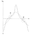
そして、図1に示されるように、高周波ジェネレータの出力電圧波形にリンギング現象(波形が一部区間で歪む現象、A1、A2)が発生すると、負荷であるプラズマチャンバの上部電極でスパークが発生する可能性が高まる。プラズマチャンバの上部電極に発生するスパークがチャンバ内のウエハに落下すると、当該ウエハは不良で廃棄しなければならないので、これも歩留まりに大きな影響を及ぼす。ところで、出力電圧波形に現れるリンギング現象は、高周波ジェネレータ内に配置されたトランスフォーマの漏れインダクタンスと容量性負荷であるプラズマチャンバとの結合による共振によって発生すると把握される。一方、プラズマチャンバが要求する高周波ジェネレータの出力電力は、負荷の状況によって随時変化するため、その制御がなおさら容易でない。 Then, as shown in FIG. 1, when a ringing phenomenon (a phenomenon in which the waveform is distorted in a part of a section, A1 and A2) occurs in the output voltage waveform of the high-frequency generator, sparks occur in the upper electrode of the plasma chamber, which is a load. The possibility increases. When the spark generated in the upper electrode of the plasma chamber falls on the wafer in the chamber, the wafer is defective and must be discarded, which also has a great influence on the yield. By the way, it is understood that the ringing phenomenon appearing in the output voltage waveform is generated by resonance due to the coupling between the leakage inductance of the transformer arranged in the high frequency generator and the plasma chamber which is a capacitive load. On the other hand, the output power of the high-frequency generator required by the plasma chamber changes at any time depending on the load condition, so its control is not even easier.
したがって、高周波ジェネレータでは、出力周波数と出力電圧波形が非常に精密に制御される必要がある。 Therefore, in a high frequency generator, the output frequency and output voltage waveform need to be controlled very precisely.
上記の問題点を解決するためになされた本発明は、出力電流の過渡現象を防止できる高周波ジェネレータおよびその動作方法を提供することを目的とする。 An object of the present invention made to solve the above problems is to provide a high frequency generator capable of preventing a transient phenomenon of an output current and an operation method thereof.
また、本発明は、出力電流波形のリンギング現象を防止できる高周波ジェネレータおよびその動作方法を提供することを他の目的とする。 Another object of the present invention is to provide a high frequency generator capable of preventing the ringing phenomenon of the output current waveform and an operation method thereof.
さらに、本発明は、出力電流を精密に制御できる高周波ジェネレータおよびその動作方法を提供することをさらに他の目的とする。 Furthermore, another object of the present invention is to provide a high frequency generator capable of precisely controlling the output current and a method of operating the same.
本発明の一態様に係る高周波ジェネレータは、商用電源の交流電圧を直流電圧に整流して出力する整流部と、前記整流部から出力される直流電圧を第2直流電圧に変換するDC/DCコンバータと、PWM制御信号で制御される交互に動作する第1および第2スイッチング素子を含み、前記DC/DCコンバータから出力される所定レベルの直流電圧を所定レベルの交流電圧に変換するインバータと、前記インバータの出力端に直並列に結合されたインダクタおよびキャパシタを備え、前記インバータから出力される高周波信号から所定の共振周波数を有するサイン波形の共振信号を出力するLCフィルタと、前記LCフィルタから出力されるパルス波形の高周波電力信号を2次側に誘導するトランスフォーマと、高周波負荷検出電流がイグニッション負荷設定電流より大きければ、イグニッションモードを終了し、イグニッションモード終了時のスイッチング周波数をイグニッションモード離脱周波数にセットし、モード選択信号を出力するイグニッションモジュールと、前記イグニッションモジュールから出力されるイグニッションモード離脱周波数を運転モード時のスイッチング周波数の初期値に適用する運転モジュールと、前記スイッチング周波数を用いて、前記PWM制御信号を生成する信号制御部とを含む。 The high frequency generator according to one aspect of the present invention includes a rectifying unit that rectifies the AC voltage of a commercial power supply to a DC voltage and outputs it, and a DC / DC converter that converts the DC voltage output from the rectifying unit into a second DC voltage. An inverter that includes first and second switching elements that operate alternately and is controlled by a PWM control signal, and converts a predetermined level of DC voltage output from the DC / DC converter into a predetermined level of AC voltage. An LC filter having an inductor and a capacitor coupled in series and parallel to the output end of the inverter and outputting a sine waveform resonance signal having a predetermined resonance frequency from a high frequency signal output from the inverter, and an LC filter output from the LC filter. If the high-frequency power signal of the pulse waveform is induced to the secondary side and the high-frequency load detection current is larger than the ignition load set current, the ignition mode is terminated and the switching frequency at the end of the ignition mode is set to the ignition mode exit frequency. The PWM control is performed using the ignition module that outputs the mode selection signal, the operation module that applies the ignition mode departure frequency output from the ignition module to the initial value of the switching frequency in the operation mode, and the switching frequency. It includes a signal control unit that generates a signal.
また、本発明の他の態様に係る高周波ジェネレータは、商用電源の交流電圧を直流電圧に整流して出力する整流部と、前記整流部から出力される直流電圧を第2直流電圧に変換するDC/DCコンバータと、PWM制御信号で制御される交互に動作する第1および第2スイッチング素子を含み、前記DC/DCコンバータから出力される所定レベルの直流電圧を所定レベルの交流電圧に変換するインバータと、前記インバータの出力端に直並列に結合されたインダクタおよびキャパシタを備え、前記インバータから出力される高周波信号から所定の共振周波数を有するサイン波形の共振信号を出力するLCフィルタと、前記LCフィルタから出力されるパルス波形の高周波電力信号を2次側に誘導するトランスフォーマと、高周波負荷側の高周波負荷検出電流と高周波負荷検出電圧とを用いて、前記PWM制御信号を生成する信号制御部とを含む。 Further, the high frequency generator according to another aspect of the present invention has a rectifying unit that rectifies the AC voltage of a commercial power supply to a DC voltage and outputs it, and a DC that converts the DC voltage output from the rectifying unit into a second DC voltage. An inverter that includes a / DC converter and alternating first and second switching elements controlled by PWM control signals, and converts a predetermined level of DC voltage output from the DC / DC converter into a predetermined level of AC voltage. An LC filter having an inductor and a capacitor coupled in series and parallel to the output end of the inverter and outputting a sine waveform resonance signal having a predetermined resonance frequency from the high frequency signal output from the inverter, and the LC filter. A transformer that induces a high-frequency power signal of a pulse waveform output from the secondary side, and a signal control unit that generates the PWM control signal by using a high-frequency load detection current and a high-frequency load detection voltage on the high-frequency load side. Including.
さらに、本発明の他の態様に係る高周波ジェネレータの動作方法は、イグニッションモードと運転モードとで動作する高周波ジェネレータの動作方法において、前記高周波ジェネレータがイグニッションモードに入る第1ステップと、イグニッションモジュールが、高周波負荷側で検出される高周波負荷検出電流とイグニッション負荷設定電流とを比較する第2ステップと、高周波負荷検出電流がイグニッション負荷設定電流より小さければ、前記イグニッションモジュールが、高周波負荷側で検出される高周波負荷検出電圧とイグニッション負荷設定電圧とを比較する第3ステップと、高周波負荷検出電流がイグニッション負荷設定電流より大きいか等しければ、前記イグニッションモジュールは、イグニッションモードを終了し、終了時のスイッチング周波数をイグニッションモード離脱周波数にセットする第4ステップと、高周波負荷検出電圧がイグニッション負荷設定電圧より小さければ、前記イグニッションモジュールは、スイッチング周波数を所定周波数だけ減少させ、前記第2ステップに戻る第5ステップと、高周波負荷検出電圧がイグニッション負荷設定電圧より大きければ、前記イグニッションモジュールは、スイッチング周波数を現在通りに維持したまま、前記第2ステップに戻る第6ステップと、運転モジュールが、イグニッションモード離脱周波数を運転モードにおけるスイッチング周波数の初期値に適用し、高周波負荷検出電流と外部から入力される高周波負荷設定電流とを用いて、スイッチング周波数を生成する第7ステップとを含む。 Further, in the operation method of the high frequency generator according to another aspect of the present invention, in the operation method of the high frequency generator operating in the ignition mode and the operation mode, the first step in which the high frequency generator enters the ignition mode and the ignition module are used. The second step of comparing the high frequency load detection current detected on the high frequency load side with the ignition load setting current, and if the high frequency load detection current is smaller than the ignition load setting current, the ignition module is detected on the high frequency load side. If the third step of comparing the high-frequency load detection voltage and the ignition load set voltage is equal to whether the high-frequency load detection current is larger than the ignition load set current, the ignition module exits the ignition mode and sets the switching frequency at the end. The fourth step of setting the ignition mode departure frequency, and the fifth step of reducing the switching frequency by a predetermined frequency and returning to the second step if the high frequency load detection voltage is smaller than the ignition load set voltage. If the high-frequency load detection voltage is larger than the ignition load set voltage, the ignition module keeps the switching frequency as it is, and the sixth step returns to the second step, and the operation module sets the ignition mode departure frequency to the operation mode. It is applied to the initial value of the switching frequency in, and includes the seventh step of generating the switching frequency by using the high frequency load detection current and the high frequency load setting current input from the outside.
本発明の高周波ジェネレータによれば、イグニッションモードから定常状態モードへの遷移時、出力電流の過渡現象を防止し、出力電流波形におけるリンギング現象を防止することにより、負荷である高周波チャンバでの歩留まりを大幅に向上させることができる効果がある。 According to the high-frequency generator of the present invention, when transitioning from the ignition mode to the steady state mode, the transient phenomenon of the output current is prevented, and the ringing phenomenon in the output current waveform is prevented, thereby reducing the yield in the high-frequency chamber which is the load. There is an effect that can be greatly improved.
以下、添付した図面を参照して、本発明に係る具体的な実施形態が説明される。しかし、これは、本発明を特定の実施形態について限定しようとするものではなく、本発明の思想および技術範囲に含まれるあらゆる変更、均等物、代替物を含むことが理解されなければならない。 Hereinafter, specific embodiments according to the present invention will be described with reference to the attached drawings. However, this is not intended to limit the invention to any particular embodiment, and it should be understood to include all modifications, equivalents and alternatives contained within the ideas and technical scope of the invention.
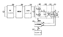
図2は、本発明の一実施形態に係る高周波ジェネレータのブロック図である。 FIG. 2 is a block diagram of a high frequency generator according to an embodiment of the present invention.
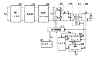
本発明の一実施形態に係る高周波ジェネレータは、EMIフィルタ201と、整流部203と、DC/DCコンバータ205と、インバータ207と、LCフィルタ209と、トランスフォーマ211と、リンギング除去部213と、信号制御部215と、インジケータ217とを含む。
The high-frequency generator according to the embodiment of the present invention includes an
EMIフィルタ201は、印加される単相交流電源に含まれた電磁波のノイズを遮蔽する機能を担う。
The
整流部203は、商用電源の交流電圧を直流電圧に整流して出力する。
The rectifying
DC/DCコンバータ205は、整流部203から出力される直流電圧を第2直流電圧に変換する。ここで、第2直流電圧は、多様なレベルの電圧でありうる。
The DC /
インバータ207は、PWM制御信号で制御されるスイッチング素子S1、S2を用いて、DC/DCコンバータ205から出力される所定レベルの直流電圧を所定レベルの交流電圧に変換する。インバータ207内の第1スイッチS1および第2スイッチS2は、交互に動作する。
The
LCフィルタ209は、直並列に結合されたインダクタおよびキャパシタを備え、インバータ207から出力される高周波信号から所定の共振周波数を有するサイン波形の共振信号を出力する。一実施形態によれば、共振信号の共振周波数は、13.56MHzでありうる。
The
トランスフォーマ211は、LCフィルタ209から出力されるパルス波形の高周波電力信号を2次側に誘導し、1次側と2次側を電気的に絶縁することにより、使用者がRF負荷に含まれたプラズマチャンバを接触する場合の感電事故を予防することができる。
The
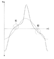
リンギング除去部213は、トランスフォーマ211の2次側に並列連結されたキャパシタC4を含む。リンギング除去部213は、トランスフォーマ211の2次側に存在する漏れインダクタンス成分と高周波負荷に寄生する寄生キャパシタンス成分による共振現象によって高周波負荷電流波形に現れるリンギング現象を除去することができる。つまり、図1と対比する時、図3に示されるように、B1領域とB2領域でリンギング現象が無くなることを確認することができる。また、リンギング除去部213のキャパシタンスC4は、トランスフォーマ211の1次側からみた時、C=C4/n2で現れるため、小容量のキャパシタを用いてもLCフィルタ209の共振利得を大幅に向上させることができるという利点がある。
The ringing removing
信号制御部215は、高周波負荷側の高周波負荷検出電流iRFおよび高周波負荷検出電圧vRFが入力され、PWM制御信号を生成してインバータ207に出力し、インジケータ217に高周波負荷検出電流iRFの状態を表示するように状態信号Sindを出力する。
The
インジケータ217は、信号制御部215から出力される状態信号Sindを用いて、高周波負荷検出電流iRFの状態を表示する。
図4は、本発明の他の実施形態に係る高周波ジェネレータのブロック図である。 FIG. 4 is a block diagram of a high frequency generator according to another embodiment of the present invention.
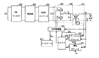
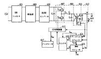
本発明の他の実施形態に係る高周波ジェネレータは、EMIフィルタ401と、整流部403と、DC/DCコンバータ405と、インバータ407と、LCフィルタ409と、トランスフォーマ411と、信号制御部415と、インジケータ417と、イグニッションモジュール421と、運転モジュール423と、セレクタ425とを含む。
The high-frequency generator according to another embodiment of the present invention includes an
図4に示された本発明の他の実施形態に係るEMIフィルタ401、整流部403、DC/DCコンバータ405、インバータ407、LCフィルタ409、トランスフォーマ411、インジケータ417の構成および機能は、図2に示されたEMIフィルタ201、整流部203、DC/DCコンバータ205、インバータ207、LCフィルタ209、トランスフォーマ211、およびインジケータ217の構成および機能と大同小異であるので、省略する。
The configurations and functions of the
イグニッションモジュール421は、イグニッションモード(ignition mode)時、高周波負荷側の高周波負荷検出電流iRFおよび高周波負荷検出電圧vRFが入力され、スイッチング周波数fsを所定のイグニッションモード開始周波数fig_stからイグニッションモード終了周波数fig_spに到達するまで所定間隔ごとに所定周波数だけ減少させる。イグニッションモジュール421は、高周波負荷検出電流iRFがイグニッション負荷設定電流iRF_ignitionより小さければ、スイッチング周波数fsを減少させ、高周波負荷検出電流iRFがイグニッション負荷設定電流iRF_ignitionより大きいか等しければ、イグニッションモード(ignition mode)を終了するとともに、モード選択信号Sselを出力する。また、イグニッションモジュール421は、イグニッションモード終了当時のスイッチング周波数fsをイグニッションモード離脱周波数fig_escにセットし、出力する。
When the
運転モジュール423は、イグニッションモジュール421から出力されるイグニッションモード離脱周波数fig_escを運転モードにおけるスイッチング周波数fsの初期値に適用し、この後、高周波負荷検出電流iRFと外部から入力される高周波負荷設定電流

セレクタ425は、イグニッションモード時には、イグニッションモジュール421から出力されるスイッチング周波数fsを選択し、イグニッションモード終了時、イグニッションモジュール421から出力されるモード選択信号Sselで制御され、運転モード時には、運転モジュール423から出力されるスイッチング周波数fsを選択する。
The selector 425, the ignition mode, select the switching frequency f s that is output from the
信号制御部415は、セレクタ425から出力されるスイッチング周波数fsを用いて、PWM制御信号を生成してインバータ407に出力し、高周波負荷検出電流iRFが入力され、インジケータ417に高周波負荷検出電流iRFの状態を表示するように状態信号Sindを出力する。
The
図5は、本発明のさらに他の実施形態に係る高周波ジェネレータのブロック図である。
本発明のさらに他の実施形態に係る高周波ジェネレータは、EMIフィルタ501と、整流部503と、DC/DCコンバータ505と、インバータ507と、LCフィルタ509と、トランスフォーマ511と、リンギング除去部513と、信号制御部515と、インジケータ517と、イグニッションモジュール521と、運転モジュール523と、セレクタ525とを含む。
FIG. 5 is a block diagram of a high frequency generator according to still another embodiment of the present invention.
The high frequency generator according to still another embodiment of the present invention includes an
つまり、図5に示された本発明のさらに他の実施形態に係る高周波ジェネレータは、図4に示された本発明の他の実施形態に係る高周波ジェネレータにリンギング除去部513が追加されたものである。
That is, the high-frequency generator according to still another embodiment of the present invention shown in FIG. 5 is a high-frequency generator according to another embodiment of the present invention shown in FIG. 4 with the
図6は、本発明のさらに他の実施形態に係る高周波ジェネレータのブロック図である。 FIG. 6 is a block diagram of a high frequency generator according to still another embodiment of the present invention.
図6に示された本発明のさらに他の実施形態に係る高周波ジェネレータは、EMIフィルタ601と、整流部603と、DC/DCコンバータ605と、インバータ607と、LCフィルタ609と、トランスフォーマ611と、リンギング除去部613と、信号制御部615と、インジケータ617と、イグニッションモジュール621と、運転モジュール623と、セレクタ625とを含む。
The high frequency generator according to still another embodiment of the present invention shown in FIG. 6 includes an
つまり、図6に示された本発明のさらに他の実施形態に係る高周波ジェネレータは、図5に示された本発明のさらに他の実施形態に係る高周波ジェネレータ内のキャパシタのみからなるリンギング除去部513の代わりに、直列連結された抵抗およびキャパシタからなるリンギング除去部613を適用したことから相違がある。
That is, the high-frequency generator according to still another embodiment of the present invention shown in FIG. 6 is a
リンギング除去部を、キャパシタのみから構成することより、直列連結された抵抗およびキャパシタから構成すれば、ダンピング効果を極大化することができる。 The damping effect can be maximized if the ringing removing portion is composed of a resistor and a capacitor connected in series rather than being composed of only a capacitor.
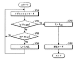
図7は、本発明の一実施形態に係る高周波ジェネレータの制御フロー図である。 FIG. 7 is a control flow diagram of a high frequency generator according to an embodiment of the present invention.
本発明の一実施形態に係る高周波ジェネレータは、高周波制御のためにイグニッションモードに入ると(S710)、イグニッションモジュール421、521、621は、高周波負荷検出電流iRFとイグニッション負荷設定電流iRF_ignitionとを比較する(S720)。
When the high-frequency generator according to the embodiment of the present invention enters the ignition mode for high-frequency control (S710), the
高周波負荷検出電流iRFがイグニッション負荷設定電流iRF_ignitionより小さければ、イグニッションモジュール421、521、621は、高周波負荷検出電圧vRFとイグニッション負荷設定電圧vRF_limitとを比較する(S730)。
If the high frequency load detection current i RF is smaller than the ignition load setting current i RF_ignition , the
高周波負荷検出電流iRFがイグニッション負荷設定電流iRF_ignitionより大きいか等しければ、イグニッションモジュール421、521、621は、イグニッションモードを終了し、終了時のスイッチング周波数をイグニッションモード離脱周波数fig_escにセットする(S740)。
If the high-frequency load detection current i RF is greater than or equal to the ignition load setting current i RF_ignition , the
高周波負荷検出電圧vRFがイグニッション負荷設定電圧vRF_limitより小さければ、イグニッションモジュール421、521、621は、スイッチング周波数fsを所定周波数△fsだけ減少させ(S750)、ステップS710に戻る。
If the high-frequency load detection voltage v RF is smaller than the ignition load set voltage v RF_limit , the
高周波負荷検出電圧vRFがイグニッション負荷設定電圧vRF_limitより大きいか等しければ、イグニッションモジュール421、521、621は、スイッチング周波数fsを現在通りに維持したまま、ステップS710に戻る。 Equal frequency load detection voltage v RF is the ignition load setting voltage v or RF_limit larger, the ignition module 421,521,621 while maintaining the switching frequency f s to the current street, the flow returns to step S710.
運転モジュール423、523、623は、イグニッションモード離脱周波数fig_escを運転モードにおけるスイッチング周波数fsの初期値に適用し、高周波負荷検出電流iRFと外部から入力される高周波負荷設定電流
上記に開示された発明は、基本的な思想を損なわない範囲内で多様な変形例が可能である。つまり、上記の実施形態はすべて例示的に解釈されなければならず、限定的に解釈されない。したがって、本発明の保護範囲は、上述した実施形態ではなく、添付した請求項によって定められなければならず、添付した請求項に限定された構成要素を均等物に置換した場合、これは、本発明の保護範囲に属すると見なさなければならない。 The invention disclosed above can be modified in various ways within a range that does not impair the basic idea. That is, all of the above embodiments must be interpreted exemplarily and not in a limited way. Therefore, the scope of protection of the present invention must be defined by the attached claims, not by the above-described embodiment, and when the components limited to the attached claims are replaced with equivalents, this is the present invention. It must be considered to belong to the scope of protection of the invention.
201、401、501、601:EMIフィルタ
203、403、503、603:整流部
205、405、505、605:DC/DCコンバータ
207、407、507、607:インバータ
209、409、509、609:LCフィルタ
211、411、511、611:トランスフォーマ
213、413、513、613:リンギング除去部
215、415、515、615:信号制御部
217、417、517、617:インジケータ
421、521、621:イグニッションモジュール
423、523、623:運転モジュール
425、525、625:セレクタ
201, 401, 501, 601:
Claims (13)
前記整流部から出力される直流電圧を第2直流電圧に変換するDC/DCコンバータと、
PWM制御信号で制御される交互に動作する第1および第2スイッチング素子を含み、前記DC/DCコンバータから出力される所定レベルの直流電圧を所定レベルの交流電圧に変換するインバータと、
前記インバータの出力端に直並列に結合されたインダクタおよびキャパシタを備え、前記インバータから出力される高周波信号から所定の共振周波数を有するサイン波形の共振信号を出力するLCフィルタと、
前記LCフィルタから出力されるパルス波形の高周波電力信号を2次側に誘導するトランスフォーマと、
高周波負荷検出電流がイグニッション負荷設定電流より大きければ、イグニッションモードを終了し、イグニッションモード終了時のスイッチング周波数をイグニッションモード離脱周波数にセットし、モード選択信号を出力するイグニッションモジュールと、
前記イグニッションモジュールから出力されるイグニッションモード離脱周波数を運転モード時のスイッチング周波数の初期値に適用する運転モジュールと、
前記スイッチング周波数を用いて、前記PWM制御信号を生成する信号制御部とを含む高周波ジェネレータ。 A rectifier that rectifies the AC voltage of a commercial power supply to a DC voltage and outputs it,
A DC / DC converter that converts the DC voltage output from the rectifier to a second DC voltage,
An inverter that includes alternating first and second switching elements controlled by PWM control signals and converts a predetermined level of DC voltage output from the DC / DC converter into a predetermined level of AC voltage.
An LC filter having an inductor and a capacitor coupled in series and parallel to the output end of the inverter and outputting a sine waveform resonance signal having a predetermined resonance frequency from a high frequency signal output from the inverter.
A transformer that guides the high-frequency power signal of the pulse waveform output from the LC filter to the secondary side, and
If the high-frequency load detection current is larger than the ignition load set current, the ignition mode is terminated, the switching frequency at the end of the ignition mode is set to the ignition mode exit frequency, and the ignition module that outputs the mode selection signal.
An operation module that applies the ignition mode departure frequency output from the ignition module to the initial value of the switching frequency in the operation mode, and
A high frequency generator including a signal control unit that generates the PWM control signal using the switching frequency.
前記状態信号に応答して前記高周波負荷検出電流の状態を表示するインジケータをさらに含む、請求項4に記載の高周波ジェネレータ。 The signal control unit receives a high-frequency load detection current and outputs a status signal so as to display the status of the high-frequency load detection current.
The high frequency generator according to claim 4, further comprising an indicator that displays the state of the high frequency load detection current in response to the state signal.
高周波負荷側で検出される高周波負荷検出電流とイグニッション負荷設定電流とを比較し、高周波負荷検出電流がイグニッション負荷設定電流より小さければ、高周波負荷側で検出される高周波負荷検出電圧とイグニッション負荷設定電圧とを比較し、高周波負荷検出電流がイグニッション負荷設定電流より大きいか等しければ、イグニッションモードを終了し、終了時のスイッチング周波数をイグニッションモード離脱周波数にセットし、高周波負荷検出電圧がイグニッション負荷設定電圧より小さければ、スイッチング周波数を所定周波数だけ減少させ、高周波負荷検出電圧がイグニッション負荷設定電圧より大きければ、スイッチング周波数を現在通りに維持し、
前記運転モジュールは、イグニッションモード離脱周波数を運転モードにおけるスイッチング周波数の初期値に適用する、請求項2に記載の高周波ジェネレータ。 The ignition module is
Compare the high frequency load detection current detected on the high frequency load side with the ignition load setting current, and if the high frequency load detection current is smaller than the ignition load setting current, the high frequency load detection voltage and ignition load setting voltage detected on the high frequency load side If the high frequency load detection current is greater than or equal to the ignition load set current, exit the ignition mode, set the switching frequency at the end to the ignition mode exit frequency, and the high frequency load detection voltage is higher than the ignition load set voltage. If it is small, the switching frequency is reduced by a predetermined frequency, and if the high frequency load detection voltage is larger than the ignition load set voltage, the switching frequency is maintained as it is.
The high-frequency generator according to claim 2, wherein the operation module applies an ignition mode departure frequency to an initial value of a switching frequency in the operation mode.
前記整流部から出力される直流電圧を第2直流電圧に変換するDC/DCコンバータと、
PWM制御信号で制御される交互に動作する第1および第2スイッチング素子を含み、前記DC/DCコンバータから出力される所定レベルの直流電圧を所定レベルの交流電圧に変換するインバータと、
前記インバータの出力端に直並列に結合されたインダクタおよびキャパシタを備え、前記インバータから出力される高周波信号から所定の共振周波数を有するサイン波形の共振信号を出力するLCフィルタと、
前記LCフィルタから出力されるパルス波形の高周波電力信号を2次側に誘導するトランスフォーマと、
高周波負荷側の高周波負荷検出電流と高周波負荷検出電圧とを用いて、前記PWM制御信号を生成する信号制御部とを含む高周波ジェネレータ。 A rectifier that rectifies the AC voltage of a commercial power supply to a DC voltage and outputs it,
A DC / DC converter that converts the DC voltage output from the rectifier to a second DC voltage,
An inverter that includes alternating first and second switching elements controlled by PWM control signals and converts a predetermined level of DC voltage output from the DC / DC converter into a predetermined level of AC voltage.
An LC filter having an inductor and a capacitor coupled in series and parallel to the output end of the inverter and outputting a sine waveform resonance signal having a predetermined resonance frequency from a high frequency signal output from the inverter.
A transformer that guides the high-frequency power signal of the pulse waveform output from the LC filter to the secondary side, and
A high-frequency generator including a signal control unit that generates the PWM control signal by using the high-frequency load detection current and the high-frequency load detection voltage on the high-frequency load side.
前記状態信号に応答して前記高周波負荷検出電流の状態を表示するインジケータをさらに含む、請求項9に記載の高周波ジェネレータ。 The signal control unit receives a high-frequency load detection current and outputs a status signal so as to display the status of the high-frequency load detection current.
The high frequency generator according to claim 9, further comprising an indicator that displays the state of the high frequency load detection current in response to the state signal.
前記高周波ジェネレータがイグニッションモードに入る第1ステップと、
イグニッションモジュールが、高周波負荷側で検出される高周波負荷検出電流とイグニッション負荷設定電流とを比較する第2ステップと、
高周波負荷検出電流がイグニッション負荷設定電流より小さければ、前記イグニッションモジュールが、高周波負荷側で検出される高周波負荷検出電圧とイグニッション負荷設定電圧とを比較する第3ステップと、
高周波負荷検出電流がイグニッション負荷設定電流より大きいか等しければ、前記イグニッションモジュールは、イグニッションモードを終了し、終了時のスイッチング周波数をイグニッションモード離脱周波数にセットする第4ステップと、
高周波負荷検出電圧がイグニッション負荷設定電圧より小さければ、前記イグニッションモジュールは、スイッチング周波数を所定周波数だけ減少させ、前記第2ステップに戻る第5ステップと、
高周波負荷検出電圧がイグニッション負荷設定電圧より大きければ、前記イグニッションモジュールは、スイッチング周波数を現在通りに維持したまま、前記第2ステップに戻る第6ステップと、
運転モジュールが、イグニッションモード離脱周波数を運転モードにおけるスイッチング周波数の初期値に適用し、高周波負荷検出電流と外部から入力される高周波負荷設定電流とを用いて、スイッチング周波数を生成する第7ステップとを含む高周波ジェネレータの動作方法。 In the operation method of the high frequency generator that operates in the ignition mode and the operation mode,
The first step in which the high frequency generator enters the ignition mode,
The second step in which the ignition module compares the high-frequency load detection current detected on the high-frequency load side with the ignition load set current, and
If the high-frequency load detection current is smaller than the ignition load set current, the ignition module compares the high-frequency load detection voltage detected on the high-frequency load side with the ignition load set voltage in the third step.
If the high-frequency load detection current is greater than or equal to the ignition load set current, the ignition module exits the ignition mode and sets the switching frequency at the end to the ignition mode exit frequency.
If the high-frequency load detection voltage is smaller than the ignition load set voltage, the ignition module reduces the switching frequency by a predetermined frequency and returns to the second step in the fifth step.
If the high-frequency load detection voltage is larger than the ignition load set voltage, the ignition module returns to the second step while maintaining the switching frequency as it is, and the sixth step.
The operation module applies the ignition mode departure frequency to the initial value of the switching frequency in the operation mode, and uses the high frequency load detection current and the high frequency load setting current input from the outside to generate the switching frequency. How to operate the high frequency generator including.
Applications Claiming Priority (2)
| Application Number | Priority Date | Filing Date | Title |
|---|---|---|---|
| KR1020190053516A KR102242234B1 (en) | 2019-05-08 | 2019-05-08 | Rf generator and its operating method |
| KR10-2019-0053516 | 2019-05-08 |
Publications (2)
| Publication Number | Publication Date |
|---|---|
| JP2020184870A true JP2020184870A (en) | 2020-11-12 |
| JP6802577B2 JP6802577B2 (en) | 2020-12-16 |
Family
ID=72944648
Family Applications (1)
| Application Number | Title | Priority Date | Filing Date |
|---|---|---|---|
| JP2019110832A Expired - Fee Related JP6802577B2 (en) | 2019-05-08 | 2019-06-14 | High frequency generator and how it works |
Country Status (4)
| Country | Link |
|---|---|
| US (2) | US10818474B1 (en) |
| JP (1) | JP6802577B2 (en) |
| KR (1) | KR102242234B1 (en) |
| TW (1) | TWI714126B (en) |
Families Citing this family (4)
| Publication number | Priority date | Publication date | Assignee | Title |
|---|---|---|---|---|
| US11146164B2 (en) * | 2020-01-21 | 2021-10-12 | The Florida State University Research Foundation, Inc. | Single transformer-based gate driver |
| WO2023081110A1 (en) * | 2021-11-03 | 2023-05-11 | Lam Research Corporation | Method and apparatus for automated regulation of a frequency-modulated multilevel outphasing power amplifier |
| CN115664177A (en) * | 2022-10-20 | 2023-01-31 | 华为数字能源技术有限公司 | Distribution circuit and power supply system of uninterrupted power supply |
| CN117545162B (en) * | 2023-11-08 | 2024-05-28 | 江苏神州半导体科技有限公司 | A remote plasma source pre-ignition device and control method thereof |
Family Cites Families (17)
| Publication number | Priority date | Publication date | Assignee | Title |
|---|---|---|---|---|
| JP3603643B2 (en) * | 1999-02-15 | 2004-12-22 | 松下電工株式会社 | Discharge lamp lighting device |
| TW428847U (en) * | 1999-06-05 | 2001-04-01 | Ind Tech Res Inst | Conversion circuit for ringing current choke with dual factor feedback control |
| TW501334B (en) * | 2001-01-20 | 2002-09-01 | Skynet Electronic Co Ltd | Ringing-free zero-voltage switching method for power converter |
| US6522089B1 (en) * | 2001-10-23 | 2003-02-18 | Orsam Sylvania Inc. | Electronic ballast and method for arc straightening |
| JP2006211877A (en) | 2005-01-31 | 2006-08-10 | Tdk Corp | Switching power unit |
| JP4418424B2 (en) | 2005-11-21 | 2010-02-17 | 日本リライアンス株式会社 | AC power supply apparatus and arc suppression method in the apparatus |
| KR101391874B1 (en) * | 2008-01-10 | 2014-05-07 | (주) 이이시스 | Device for controlling high voltage having capacitive load property |
| US7721697B2 (en) * | 2008-01-31 | 2010-05-25 | West Virginia University | Plasma generating ignition system and associated method |
| CN102458027B (en) * | 2010-10-22 | 2014-05-07 | 台达电子工业股份有限公司 | Lighting circuit control method and applicable lighting circuit |
| US8786371B2 (en) * | 2011-11-18 | 2014-07-22 | Skyworks Solutions, Inc. | Apparatus and methods for voltage converters |
| DE12884309T1 (en) * | 2012-09-05 | 2015-09-17 | Kyosan Electric Mfg. Co., Ltd. | DC POWER SUPPLY AND CONTROL PROCEDURE FOR THE DC POWER SUPPLY |
| IN2014KN03106A (en) | 2012-09-07 | 2015-05-08 | Kyosan Electric Mfg | |
| JP6107132B2 (en) | 2012-12-28 | 2017-04-05 | 富士電機株式会社 | Switching power supply |
| JP5729732B2 (en) | 2013-09-27 | 2015-06-03 | 株式会社京三製作所 | DC power supply and control method of DC power supply |
| JP6413261B2 (en) * | 2014-03-03 | 2018-10-31 | 株式会社島津製作所 | High frequency power supply for ICP emission analyzer |
| JP6414676B2 (en) * | 2014-09-10 | 2018-10-31 | パナソニックIpマネジメント株式会社 | Lighting device and lighting apparatus |
| JP5788616B1 (en) * | 2015-02-04 | 2015-10-07 | 株式会社京三製作所 | High frequency power supply and dual cathode power supply |
-
2019
- 2019-05-08 KR KR1020190053516A patent/KR102242234B1/en active Active
- 2019-05-24 US US16/421,734 patent/US10818474B1/en active Active
- 2019-06-14 TW TW108120675A patent/TWI714126B/en not_active IP Right Cessation
- 2019-06-14 JP JP2019110832A patent/JP6802577B2/en not_active Expired - Fee Related
-
2020
- 2020-01-10 US US16/739,553 patent/US20200357609A1/en not_active Abandoned
Also Published As
| Publication number | Publication date |
|---|---|
| TW202042599A (en) | 2020-11-16 |
| US20200357608A1 (en) | 2020-11-12 |
| KR20200129307A (en) | 2020-11-18 |
| KR102242234B1 (en) | 2021-04-20 |
| US20200357609A1 (en) | 2020-11-12 |
| US10818474B1 (en) | 2020-10-27 |
| TWI714126B (en) | 2020-12-21 |
| JP6802577B2 (en) | 2020-12-16 |
Similar Documents
| Publication | Publication Date | Title |
|---|---|---|
| JP6802577B2 (en) | High frequency generator and how it works | |
| US9450519B2 (en) | DC power source, and DC power source control method | |
| WO2012033120A1 (en) | Power supply integrated circuit device and power supply interruption detecting method | |
| JP6758504B2 (en) | Welding current source | |
| JP3719352B2 (en) | Power supply device for plasma generation and method for manufacturing the same | |
| KR101844981B1 (en) | Llcc resonant converter for a plasma process | |
| CN109314460B (en) | Power conversion device | |
| JP2021065052A (en) | Dc pulse power supply for plasma device | |
| JP3868624B2 (en) | Power supply for plasma generation | |
| US11112446B2 (en) | Circuit arrangement for a high-voltage test installation | |
| KR102125026B1 (en) | Resonant network For Plasma Power And Power Supply Apparatus For Plasma Generator | |
| JP3206521B2 (en) | High frequency heating equipment | |
| CN105604766A (en) | Corona ignition system for an internal combustion engine | |
| WO2011010481A1 (en) | Discharge tube lighting device and method for detecting abnormal electric discharge in same | |
| JP3118849U (en) | Arc discharge protection device in current exploration mode | |
| RU2608179C2 (en) | High-frequency induction heating device protection circuit and high-frequency induction heating device with protection circuit | |
| US6075327A (en) | Power supply apparatus for a discharge lamp, especially for a motor vehicle headlight | |
| US20250044372A1 (en) | Circuit for conduction testing of power supply of plasma globe lamp | |
| US7327094B2 (en) | Circuit arrangement and method for operating at least one electric lamp | |
| TW201345157A (en) | Zero current detector for a power supplier and method thereof | |
| JP2005340185A (en) | Method for manufacturing plasma generating power supply device | |
| KR101524314B1 (en) | Apparatus for reducing sound noise | |
| KR101458933B1 (en) | Multi-level power converting system for resonance load and method for controlling the same | |
| KR20120052379A (en) | Electronic ballast for operating at least one discharge lamp | |
| JP2015095378A (en) | High voltage generation circuit and ion pump using the same |
Legal Events
| Date | Code | Title | Description |
|---|---|---|---|
| A621 | Written request for application examination |
Free format text: JAPANESE INTERMEDIATE CODE: A621 Effective date: 20190620 |
|
| A131 | Notification of reasons for refusal |
Free format text: JAPANESE INTERMEDIATE CODE: A131 Effective date: 20200818 |
|
| A521 | Request for written amendment filed |
Free format text: JAPANESE INTERMEDIATE CODE: A523 Effective date: 20200903 |
|
| TRDD | Decision of grant or rejection written | ||
| A01 | Written decision to grant a patent or to grant a registration (utility model) |
Free format text: JAPANESE INTERMEDIATE CODE: A01 Effective date: 20201110 |
|
| A61 | First payment of annual fees (during grant procedure) |
Free format text: JAPANESE INTERMEDIATE CODE: A61 Effective date: 20201119 |
|
| R150 | Certificate of patent or registration of utility model |
Ref document number: 6802577 Country of ref document: JP Free format text: JAPANESE INTERMEDIATE CODE: R150 |
|
| LAPS | Cancellation because of no payment of annual fees |