JP2020184848A - Control device, power conversion device, control method, and program - Google Patents
Control device, power conversion device, control method, and program Download PDFInfo
- Publication number
- JP2020184848A JP2020184848A JP2019088774A JP2019088774A JP2020184848A JP 2020184848 A JP2020184848 A JP 2020184848A JP 2019088774 A JP2019088774 A JP 2019088774A JP 2019088774 A JP2019088774 A JP 2019088774A JP 2020184848 A JP2020184848 A JP 2020184848A
- Authority
- JP
- Japan
- Prior art keywords
- control
- input current
- power
- switching element
- unit
- Prior art date
- Legal status (The legal status is an assumption and is not a legal conclusion. Google has not performed a legal analysis and makes no representation as to the accuracy of the status listed.)
- Pending
Links
Images

Landscapes
- Rectifiers (AREA)
Abstract
Description
本発明は、制御装置、電力変換装置、制御方法及びプログラムに関する。 The present invention relates to a control device, a power conversion device, a control method and a program.
商用電源から供給される交流電力を整流回路で直流電圧に変換し、変換後の直流電圧をインバータで交流に変換して負荷に供給する電力変換装置が提供されている。電力変換装置は、力率の改善や高調波の抑制を目的とする力率改善回路を備えている。力率改善回路は、例えば、リアクトルとスイッチング素子を備えている。このスイッチング素子のオン、オフをPAM(Pulse Amplitude Modulation)制御によって切り替えると、電力変換装置を流れる電流の波形を正弦波に近づけ、力率を改善することができる。 A power conversion device is provided in which AC power supplied from a commercial power source is converted into a DC voltage by a rectifier circuit, and the converted DC voltage is converted into AC by an inverter and supplied to a load. The power conversion device includes a power factor improving circuit for the purpose of improving the power factor and suppressing harmonics. The power factor improving circuit includes, for example, a reactor and a switching element. By switching the switching element on and off by PAM (Pulse Amplitude Modulation) control, the waveform of the current flowing through the power converter can be made closer to a sine wave, and the power factor can be improved.
電力変換装置には、安定した電圧が供給されることが望ましいが、電源のインピーダンスが大きいなど劣悪な環境下では、商用電源からの交流電圧の波形が乱れる。PAM制御を、正常な波形の交流電圧が供給されることを前提として動作させることがある。従って、電源が不安定な状態でスイッチング素子のオン、オフを切り替えると過電流が流れ、スイッチング素子の損傷を招くおそれがある。特許文献1には、不安定な入力電圧を検知すると、PAM制御を停止させて上記の課題に対処する制御が開示されている。 It is desirable that a stable voltage be supplied to the power converter, but in a poor environment such as a large impedance of the power supply, the waveform of the AC voltage from the commercial power supply is disturbed. The PAM control may be operated on the assumption that an AC voltage having a normal waveform is supplied. Therefore, if the switching element is switched on and off while the power supply is unstable, an overcurrent may flow, causing damage to the switching element. Patent Document 1 discloses a control that stops PAM control when an unstable input voltage is detected to deal with the above problems.
入力電圧が不安定なときに力率改善回路の動作を停止させると、スイッチング素子は保護されるが、入力電流には高調波成分が含まれたままとなり、力率が低下する。また、高調波の影響で過電流が流れると、電力変換装置の他の部品の損傷を招くおそれがある。 If the operation of the power factor improving circuit is stopped when the input voltage is unstable, the switching element is protected, but the input current still contains harmonic components, and the power factor decreases. Further, if an overcurrent flows due to the influence of harmonics, there is a risk of damaging other parts of the power converter.
そこでこの発明は、上述の課題を解決することのできる制御装置、電力変換装置、制御方法及びプログラムを提供することを目的としている。 Therefore, an object of the present invention is to provide a control device, a power conversion device, a control method, and a program capable of solving the above-mentioned problems.
本発明の一態様によれば、制御装置は、力率改善回路を備える電力変換装置の制御装置であって、交流電源のゼロクロスを検出する検出部と、前記ゼロクロスの周期が所定の許容範囲を外れると、前記力率改善回路のスイッチング素子のオン・オフ制御を停止するスイッチング制御部と、前記スイッチング素子のオン・オフ制御を停止した後の前記電力変換装置を流れる入力電流を評価する評価部と、前記入力電流の評価結果に基づいて、前記入力電流を抑制する制御を行う抑制部と、を備える。 According to one aspect of the present invention, the control device is a control device of a power conversion device including a power factor improving circuit, and the detection unit for detecting the zero cross of the AC power supply and the period of the zero cross have a predetermined allowable range. When it comes off, a switching control unit that stops the on / off control of the switching element of the power factor improvement circuit and an evaluation unit that evaluates the input current flowing through the power conversion device after stopping the on / off control of the switching element. And a suppression unit that controls to suppress the input current based on the evaluation result of the input current.
本発明の一態様によれば、前記評価部は、前記入力電流のピーク値と実効値の差が所定の閾値以上となると、前記入力電流に含まれる高周波成分が過多であると判定する。 According to one aspect of the present invention, the evaluation unit determines that the high frequency component contained in the input current is excessive when the difference between the peak value and the effective value of the input current becomes a predetermined threshold value or more.
本発明の一態様によれば、前記抑制部は、前記評価部によって高周波成分が過多であると判定されると、前記電力変換装置の負荷を低下させる。 According to one aspect of the present invention, the suppression unit reduces the load on the power conversion device when the evaluation unit determines that the high frequency component is excessive.
本発明の一態様によれば、前記電力変換装置の負荷が圧縮機であって、前記抑制部は、前記圧縮機の回転数を低下させる。 According to one aspect of the present invention, the load of the power conversion device is a compressor, and the suppression unit reduces the rotation speed of the compressor.
本発明の一態様によれば、前記スイッチング制御部が、前記スイッチング素子のオン・オフ制御を停止した後に、前記ゼロクロスの周期が所定の許容範囲となると、前記スイッチング素子のオン・オフ制御を再開する。 According to one aspect of the present invention, after the switching control unit stops the on / off control of the switching element, when the period of the zero cross reaches a predetermined allowable range, the on / off control of the switching element is restarted. To do.
本発明の一態様によれば、前記抑制部が前記入力電流を抑制する制御を行っている間に、前記ゼロクロスの周期が所定の許容範囲となると、前記スイッチング制御部が、前記スイッチング素子のオン・オフ制御を再開する。 According to one aspect of the present invention, when the zero cross period reaches a predetermined allowable range while the suppression unit controls to suppress the input current, the switching control unit turns on the switching element. -Resume off control.
本発明の一態様によれば、電力変換装置は、上記の何れかに記載の制御装置と、スイッチング素子を備える力率改善回路を含む交流電力を直流電力に変換するコンバータと、前記コンバータが変換した直流電力を交流電力に変換するインバータと、を備える。 According to one aspect of the present invention, the power conversion device includes the control device according to any one of the above, a converter that converts AC power including a power factor improving circuit including a switching element, and the converter. It is equipped with an inverter that converts the generated DC power into AC power.
本発明の一態様によれば、制御方法は、力率改善回路を備える電力変換装置の制御方法であって、交流電源のゼロクロスを検出するステップと、前記ゼロクロスの周期が所定の許容範囲を外れると、前記力率改善回路のスイッチング素子のオン・オフ制御を停止するステップと、前記スイッチング素子のオン・オフ制御を停止した後の前記電力変換装置を流れる入力電流を評価するステップと、前記入力電流の評価結果に基づいて、前記入力電流を抑制する制御を行うステップと、を有する。 According to one aspect of the present invention, the control method is a control method of a power conversion device including a power factor improving circuit, in which a step of detecting zero cross of an AC power supply and a period of the zero cross are out of a predetermined allowable range. A step of stopping the on / off control of the switching element of the power factor improving circuit, a step of evaluating the input current flowing through the power conversion device after stopping the on / off control of the switching element, and the input. It has a step of performing control for suppressing the input current based on the evaluation result of the current.
本発明の一態様によれば、プログラムは、力率改善回路を備える電力変換装置のコンピュータに、交流電源のゼロクロスを検出するステップと、前記ゼロクロスの周期が所定の許容範囲を外れると、前記力率改善回路のスイッチング素子のオン・オフ制御を停止するステップと、前記スイッチング素子のオン・オフ制御を停止した後の前記電力変換装置を流れる入力電流を評価するステップと、前記入力電流の評価結果に基づいて、前記入力電流を抑制する制御を行うステップと、を実行させる。 According to one aspect of the present invention, the program performs the step of detecting the zero cross of the AC power supply in the computer of the power conversion device provided with the power factor improving circuit, and the force when the period of the zero cross is out of a predetermined allowable range. A step of stopping the on / off control of the switching element of the power factor improving circuit, a step of evaluating the input current flowing through the power conversion device after stopping the on / off control of the switching element, and an evaluation result of the input current. Based on the above, the step of performing control for suppressing the input current is executed.
本発明によれば、力率改善回路の動作の停止時における高周波の発生を低減することができる。 According to the present invention, it is possible to reduce the generation of high frequencies when the operation of the power factor improving circuit is stopped.
<実施形態>
以下、本発明の一実施形態による力率改善制御(高周波抑制制御)について、図1〜図6を参照して説明する。
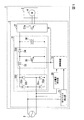
図1は、本発明の一実施形態における電力変換装置の一例を示す図である。
電力変換装置3は、空気調和機1の圧縮機2に電力を供給する。圧縮機2と、電力変換装置3とは、空気調和機1に搭載される。電力変換装置3は、交流電源5から受電した交流電力を、三相交流電力に変換して圧縮機2のモータ4に出力する。
制御装置10は、電力変換装置3を制御し、モータ4を空気調和機1の負荷に応じた回転数で駆動する。モータ4が電力変換装置3からの印加によって回転駆動することにより、圧縮機2が冷媒を圧縮し、空気調和機1が備える冷媒回路(図示せず)へ冷媒を供給する。
<Embodiment>
Hereinafter, the power factor improvement control (high frequency suppression control) according to the embodiment of the present invention will be described with reference to FIGS. 1 to 6.
FIG. 1 is a diagram showing an example of a power conversion device according to an embodiment of the present invention.
The
The
電力変換装置3は、図1に示すように、コンバータ31と、インバータ37と、制御装置10と、入力電流検出部20と、ゼロクロス検出部21と、を備える。コンバータ31は、交流電源5からの交流電力を直流電力に変換してインバータ37に出力する装置である。コンバータ31は、整流回路320と、力率改善回路330と、平滑コンデンサ36と、を備える。
As shown in FIG. 1, the
整流回路320は、ダイオード32a〜32dによって構成される。整流回路320は、交流電源5より入力された交流電力を直流電力に変換し、力率改善回路330へ出力する。
The
力率改善回路330は、平滑コンデンサ36へ電流を流し、インバータ37に入力される電圧を生成する。力率改善回路330は、リアクトル33と、ダイオード34と、スイッチング素子35と、を備える。リアクトル33は、第1端子と、第2端子と、を備える。ダイオード34は、アノード端子と、カソード端子と、を備える。スイッチング素子35は、第1端子と、第2端子と、第3端子と、を備える。スイッチング素子35は、第1端子が受ける信号に応じて、オン状態となる期間とオフ状態となる期間とが切り替わることにより、第2端子から第3端子に流れる電流を制御し、力率改善回路330に流れる電流の値を変化させる。スイッチング素子35としては、電界効果トランジスタ(FET:Field Effect Transistor)、IGBT(Insulated Gate Bipolar Transistor)等が挙げられる。スイッチング素子35が例えばnMOSトランジスタである場合、スイッチング素子35の第1端子はゲート端子であり、第2端子はソース端子であり、第3端子はドレイン端子である。力率改善回路330は、高調波抑制回路とも呼ばれる。
The power
平滑コンデンサ36は、第1端子と、第2端子と、を備える。平滑コンデンサ36は、力率改善回路330から電流を取得する。
The
インバータ37は、コンバータ31から出力された直流電力を三相交流電力に変換して圧縮機2のモータ4に出力する装置である。インバータ37のスイッチング素子37a等の第1端子は、制御装置10の第2出力端子に接続される。スイッチング素子37a等の第2端子はインバータ37が備える他のスイッチング素子、第3端子はモータ4の入力端子に接続される。制御装置10は、インバータ37が備えるブリッジ回路のスイッチング素子37a等のオンとオフを切り替える。これによりインバータ37は、三相交流電力を生成し、生成した三相交流電力をモータ4に出力する。なお、インバータ制御の具体的な手法の例としては、ベクトル制御、センサレスベクトル制御、V/F(Variable Frequency)制御、過変調制御、1パルス制御などが挙げられる。
The
入力電流検出部20は、入力端子と、出力端子と、を備える。入力電流検出部20は、交流電源5へのリターン電流(以下、「入力電流」と記載)を検出する電流計である。入力電流検出部20は、検出した入力電流の情報を制御装置10へ出力する。
The input
ゼロクロス検出部21は、第1入力端子と、第2入力端子と、出力端子と、を備える。
ゼロクロス検出部21は、第1入力端子と、第2入力端子とを介して、交流電源5が出力する電圧のゼロクロス点を検出する。ゼロクロス点は、交流電源5が出力する電圧がゼロボルトを交差する時刻を示す。ゼロクロス検出部21は、ゼロクロス点の情報を含むゼロクロス信号を生成する。ゼロクロス検出部21は、出力端子を介してゼロクロス信号を制御装置10に出力する。
The zero
The zero-
交流電源5は、出力端子と、基準端子と、を備える。交流電源5は、コンバータ31に交流電力を供給する。
The
整流回路320の入力端子(ダイオード32aのアノード端子)は、交流電源5の出力端子と、ゼロクロス検出部21の第1入力端子とに接続される。整流回路320の入力側の基準端子(ダイオード32bのアノード端子)は、交流電源5の基準端子と、ゼロクロス検出部21の第2入力端子と、入力電流検出部20の入力端子とに接続される。整流回路320の出力端子(ダイオード32a,32bのカソード端子)は、リアクトル33の第1端子に接続される。整流回路320の出力側の基準端子(ダイオード32c,32dのアノード端子)は、スイッチング素子35の第3端子と、平滑コンデンサ36の第2端子と、インバータ37の基準端子とに接続される。リアクトル33の第2端子は、ダイオード34のアノード端子と、スイッチング素子35の第2端子とに接続される。ダイオード34のカソード端子は、平滑コンデンサ36の第1端子と、インバータ37の入力端子とに接続される。
The input terminal of the rectifier circuit 320 (anode terminal of the
制御装置10は、複数の入力端子と、複数の出力端子とを備える。スイッチング素子35の第1端子は、制御装置10の第1出力端子に接続される。制御装置10の第1入力端子は、入力電流検出部20の出力端子に接続される。制御装置10の第2入力端子は、ゼロクロス検出部21の出力端子に接続される。インバータ37のスイッチング素子37a等の第1端子は、制御装置10の第2出力端子に接続される。制御装置10は、例えば、第1入力端子を介して、入力電流検出部20から入力電流の情報を取得し、入力電流の波形を監視する。制御装置10は、第2入力端子を介して、ゼロクロス検出部21からゼロクロス信号を取得し、スイッチング素子35のオンとオフを切り替えるスイッチング制御を実行する。また、制御装置10は、ゼロクロス信号を監視して、交流電源5が安定しているか否かを判定する。例えば、制御装置10は、ゼロクロスが発生する周期(ゼロクロス周期)が所定の周期かどうかを判定する。
The
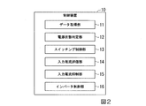
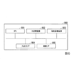
図2は、本発明の一実施形態における制御装置の一例を示すブロック図である。
制御装置10は、例えばマイコン等のCPU(Central Processing Unit)やMPU(Micro Processing Unit)を備えたコンピュータである。図示するように制御装置10は、データ取得部11と、電源状態判定部12と、スイッチング制御部13と、入力電流評価部14と、入力電流抑制部15と、インバータ制御部16とを備えている。
FIG. 2 is a block diagram showing an example of a control device according to an embodiment of the present invention.
The
データ取得部11は、入力電流検出部20から入力電流の計測値を取得する。データ取得部11は、ゼロクロス検出部21からゼロクロス信号を取得する。
The
電源状態判定部12は、データ取得部11が取得したゼロクロス信号に基づいて、交流電源5の電圧が安定して所定の周期でゼロクロスを示しているかどうかを判定する。ゼロクロスが所定の周期で検出できる場合、電源状態判定部12は、交流電源5が安定していると判定し、そうでない場合、交流電源5が不安定であると判定する。電源状態判定部12は、判定結果をスイッチング制御部13へ出力する。
The power supply
スイッチング制御部13は、電源状態判定部12による判定結果に基づいて、スイッチング素子35のオンとオフを切り替えるスイッチング制御(PAM制御)を実行又は停止する。電源状態判定部12が交流電源5は安定していると判定した場合、スイッチング制御部13は、PAM制御を実行する。一方、電源状態判定部12が交流電源5は不安定と判定した場合、スイッチング制御部13は、PAM制御を停止する。PAM制御では、入力電流の周期がゼロクロス周期と近しいと仮定して、スイッチング素子35のオンとオフを切り替えるタイミングを決定する。その為、ゼロクロス周期が不安定な場合や、ゼロクロスが正しく検出できない状態でPAM制御を行うと制御がうまく働かず、過電流が流れてスイッチング素子35の破損や劣化を招いたり、異音が生じたりする。従って、スイッチング制御部13は、ゼロクロスが正しい周期で検出できない状態が検出されると、PAM制御を停止する。
The switching
入力電流評価部14は、PAM制御停止後の入力電流を評価する。スイッチング制御部13がPAM制御を停止すると、力率改善回路330が動作しない。交流電源5が不安定な状態では、電源電圧に高周波成分が多く含まれることがある。高周波成分が含まれると力率が低下する。また、電源電圧に高周波が多く含まれる場合、例えば、平滑コンデンサ36を流れる電流にも高周波成分が多く含まれることとなり、運転の継続により平滑コンデンサ36の損傷等のリスクがある。従って、入力電流評価部14は、入力電流を監視して、入力電流に含まれる高調波が許容範囲内か否かを判定する。具体的には、入力電流評価部14は、データ取得部11が取得した入力電流のピーク値と、入力電流から計算した実効値の比に基づいて、入力電流に含まれる高周波成分が許容範囲内かどうかを評価する。例えば、(入力電流のピーク値÷入力電流の実効値)の値が所定の閾値を上回った場合、入力電流評価部14は、高周波成分が許容範囲ではない(過多)と判定する。
The input
入力電流抑制部15は、入力電流を抑制する制御を行う。入力電流を抑制すると、入力電流のピーク値が低下し、入力電流のピーク値と実効値の比が良化する。入力電流を抑制するために入力電流抑制部15は、電力変換装置3の負荷を低下させる。例えば、入力電流抑制部15は、圧縮機2の回転数を所定の閾値まで低下させる。負荷を低下させると、入力電流が抑制される。
インバータ制御部16は、インバータ37を制御し、所望の回転数でモータ4を駆動する。
The input
The
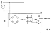
図3は、本発明の一実施形態におけるゼロクロス検出部の一例を示す概略図である。
図3に例示するようにゼロクロス検出部21は、整流回路211と、フォトカプラ212と、トランジスタ213とを備えている。整流回路211で整流された直流電圧が所定の電圧以上となるとフォトカプラ212の発光ダイオードに電流が流れ、フォトカプラ212が導通する。フォトカプラ212が導通すると、トランジスタ213が導通状態となり、制御装置10へ、ロー信号が入力される。一方、ゼロクロス点では、フォトカプラ212、トランジスタ213が導通状態とならず、制御装置10へハイ信号が入力される。
制御装置10では、電源状態判定部12がロー信号を取得している時間を計測する。計測した時間と、交流電源5の周波数(50Hzや60Hz)から算出される1周期分の時間との差が、所定の許容範囲内であれば、電源状態判定部12は、交流電源5が安定していると判定する。計測した時間と1周期分の時間との差が許容範囲外であれば、電源状態判定部12は、交流電源5が不安定であると判定する。
FIG. 3 is a schematic view showing an example of a zero cross detection unit according to an embodiment of the present invention.
As illustrated in FIG. 3, the zero-
The
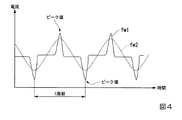
図4は、本発明の一実施形態における入力電流のピーク値を示す図である。
図4を用いて、入力電流評価部14による入力電流の評価方法を説明する。図4の波形fw1は、高調波により歪んだ入力電流の波形の一例である。波形fw2は、交流電源5の安定時に力率改善回路330が動作しているときの入力電流の波形の一例である。波形fw1、fw2は、何れも入力電流検出部20が計測した値である。入力電流評価部14は、データ取得部11を通じて波形fw1を取得すると、波形fw1のピーク値を検出する。また、入力電流評価部14は、例えば、波形fw1が示す入力電流の瞬間の値I(t)を1周期分積分した値を周期で除算し、波形fw1が示す入力電流の実効値を求める。
入力電流評価部14は、ピーク値を実効値で除算し、評価値を算出する。入力電流評価部14は、算出した評価値と所定の閾値(例えば、2の平方根)を比較して、入力電流の状態を評価する。例えば、入力電流評価部14は、評価値が閾値を上回る場合、入力電流に含まれる高調波成分は過多であると評価する。
あるいは、入力電流評価部14は、ピーク値と実効値の差を計算して、この値を評価値としてもよい。例えば、入力電流評価部14は、入力電流のピーク値から実効値を減算した値を、所定の閾値と比較して、閾値を上回る場合、入力電流に含まれる高調波成分は過多であると評価する。
FIG. 4 is a diagram showing a peak value of an input current according to an embodiment of the present invention.
The method of evaluating the input current by the input
The input
Alternatively, the input
次に図5を用いて、電源劣悪状態における本実施形態の力率改善制御(高調波抑制制御)の流れを説明する。
図5は、本発明の一実施形態における制御の一例を示すフローチャートである。
制御装置10は、インバータ37を制御し、空気調和機1の負荷に応じた回転数で圧縮機2を駆動している。また、制御装置10では、データ取得部11が、継続的に(例えば、所定の時間間隔で)、入力電流検出部20から入力電流の計測値を取得し、ゼロクロス検出部21からはゼロクロス信号(ロー信号又はハイ信号)を取得している。
電源状態判定部12は、データ取得部11が取得したゼロクロス信号に基づいて、交流電源5が安定しているか否かを判定する(ステップS11)。電源状態判定部12は、図3を用いて説明した方法により、ゼロクロス周期が所定の許容範囲内であれば、交流電源5は安定していると判定し、ロー信号を取得する時間が長かったり、短かったり、あるいは安定しない場合などには交流電源5が不安定であると判定する。
Next, with reference to FIG. 5, the flow of the power factor improvement control (harmonic suppression control) of the present embodiment in the poor power supply state will be described.
FIG. 5 is a flowchart showing an example of control according to the embodiment of the present invention.
The
The power supply
交流電源5が安定している場合(ステップS11;Yes)、スイッチング制御部13は、PAM制御を継続する(ステップS12)。例えば、スイッチング制御部13は、所定のキャリア(三角波)と交流電源5から供給される電流に含まれる基本波に相当する正弦波を示す変調波を生成する。変調波の周期はゼロクロス周期である。そして、スイッチング制御部13は、キャリアと変調波とを比較し、キャリアの値が変調波の値を上回る期間はオン、キャリアの値が変調波の値以下となる期間はオフとするスイッチング信号(PWM信号、PWM:Pulse Width Modulation)を生成する(三角波比較方式)。スイッチング制御部13が、スイッチング素子35のオン、オフを切り替えることにより、入力電流の波形を、変調波と同様の波形に制御することができる。
When the
交流電源5が安定していない場合(ステップS11;No)、スイッチング制御部13は、PAM制御を停止する(ステップS13)。つまり、スイッチング制御部13は、スイッチング素子35のオンとオフの切り替えを行わず、スイッチング素子35はオフの状態で維持される。
When the
スイッチング制御部13がPAM制御を停止すると、入力電流評価部14は、図4を用いて説明した方法により、入力電流のピーク値と実効値の関係が許容範囲内か否かを判定する(ステップS14)。例えば、入力電流評価部14は、入力電流のピーク値が実効値に比べ所定の閾値(例えば、閾値は「2」の平方根以上の値)以内であれば許容範囲内であると判定し、閾値を上回っていれば入力電流のピーク値と実効値の関係は許容範囲外(高調波成分が過多)であると判定する。許容範囲内の場合(ステップS14;Yes)、制御装置10は、PAM制御を停止させたまま、引き続き、空気調和機1の負荷に応じた回転数で圧縮機2を駆動する。
When the switching
それと並行して、電源状態判定部12は、ゼロクロス信号を監視し、交流電源5が安定化したかどうか判定を行う(ステップS15)。判定方法はステップS11と同様である。つまり、電源状態判定部12は、交流電源5の周波数に対応する正しい周期と、ゼロクロス周期との差が許容範囲内となると、交流電源5が安定化したと判定する。ステップS15の判定にあたっては、PAM制御の停止後、所定時間が経過した後にステップS15の判定を行うようにしてもよい。また、交流電源5が安定化したかどうかの判定に関して、交流電源5が安定しているとみなせる状態が、所定時間以上継続した場合に、電源が安定化したと判定してもよい。電源が安定化しない場合(ステップS15;No)、ステップS14からの処理を繰り返し行う。
At the same time, the power supply
電源が安定化すると(ステップS15;Yes)、スイッチング制御部13は、PAM制御を再開する(ステップS19)。空気調和機1の運転中、制御装置10は、再びステップS11からの処理を行う。
When the power supply stabilizes (step S15; Yes), the switching
一方、入力電流のピーク値と実効値の関係が許容範囲外の場合(ステップS14;No)、入力電流抑制部15は、入力電流を抑制する制御を行う(ステップS16)。具体的には、入力電流抑制部15は、電力変換装置3の負荷を低下させる制御を行う。例えば、高周波成分が許容範囲内となるような大きさの入力電流と、それに対応する圧縮機2の回転数Rが予め定められていて、入力電流抑制部15は、圧縮機2の回転数をRへ低下させるようにインバータ制御部16へ指示する。インバータ制御部16は、回転数Rに対応する回転数でモータ4を駆動する。圧縮機2の回転数を低下させることで入力電流を低下させ、高調波成分を抑制することができる。これにより、過電流による電子部品の損傷や劣化を防ぎ、空気調和機1を安定して運転することができる。また、空気調和機1の運転が抑えられることになるが、力率を改善することができる。
On the other hand, when the relationship between the peak value of the input current and the effective value is out of the permissible range (step S14; No), the input
入力電流を抑制した後も電源状態判定部12は、ゼロクロス信号の監視を継続し、交流電源5が安定化したかどうか判定を行う(ステップS17)。判定方法はステップS15と同様である。交流電源5が安定化しない場合(ステップS17;No)、インバータ37の負荷を低下させたまま運転を継続しつつ、ステップS17の判定を繰り返し行う。
Even after the input current is suppressed, the power supply
電源が安定化すると(ステップS17;Yes)、入力電流抑制部15は、入力電流の抑制を解除する(ステップS18)。例えば、入力電流抑制部15は、インバータ制御部16へ回転数Rの制約を解除するよう指示する。インバータ制御部16は、空気調和機1の負荷に応じた回転数でモータ4を駆動する。これにより、空気調和機1は、制約が無い状態での運転を再開する。次にスイッチング制御部13は、PAM制御を再開する(ステップS19)。制御装置10は、再びステップS11からの処理を行う。
When the power supply is stabilized (step S17; Yes), the input
力率改善回路330のスイッチング素子35に対するPAM制御は、電源電圧のゼロクロスが所定の正常周期で発生することを前提に行われる。交流電源5のゼロクロス周期が正常周期から外れているときにPAM制御を実行すると、スイッチング素子35のオンと入力電流のピーク値が重なった場合、過電流が流れてスイッチング素子などの電子部品や基板の損傷、劣化を招くおそれがある。これに対し、本実施形態では、交流電源5のゼロクロス周期が正常周期から外れる場合、PAM制御を停止するので、過電流の発生や部品等の損傷を防ぐことができる。
The PAM control for the switching
さらにPAM制御を停止すると、コンバータ31、インバータ37には、高調波成分を多く含む電流が流れるようになる。これにより、力率の低下や平滑コンデンサ36等の損傷、劣化を招くおそれがある。また、高調波が発生すると外部の機器や電源系統に影響を与える可能性がある。これに対し、本実施形態では、圧縮機2の回転数を制御して負荷を低下させるので、入力電流のピーク値および高調波成分の影響を抑制することができ、電子部品等への悪影響を防ぐことができる。また、入力電流の実効値とピーク値の比を良化し、力率を改善することができる。
Further, when the PAM control is stopped, a current containing a large amount of harmonic components flows through the
また、本実施形態によれば、上記の制御により交流電源5が不安定となる状況に対処して空気調和機1の運転を継続しつつ、交流電源5が安定化すると、入力電流の抑制を解除し、PAM制御を再開する。これにより、交流電源5が不安定な環境でも、高調波の影響を外部に及ぼすことなく、安定した運転を実現することができる。
Further, according to the present embodiment, when the
図6は、本発明の一実施形態における制御装置のハードウェア構成の一例を示す図である。コンピュータ900は、CPU901、主記憶装置902、補助記憶装置903、入出力インタフェース904、通信インタフェース905を備える例えばマイコンである。コンピュータ900は、CPU901に代えて、MPU(Micro Processing Unit)などのプロセッサを備えていてもよい。上述の制御装置10は、コンピュータ900に実装される。そして、上述した各処理部(データ取得部11、電源状態判定部12、スイッチング制御部13、入力電流評価部14、入力電流抑制部15、インバータ制御部16)の動作は、プログラムの形式で補助記憶装置903に記憶されている。CPU901は、プログラムを補助記憶装置903から読み出して主記憶装置902に展開し、当該プログラムに従って上記処理を実行する。また、CPU901は、プログラムに従って、上記処理を実行するための記憶領域を主記憶装置902に確保する。また、CPU901は、プログラムに従って、処理中のデータを記憶する記憶領域を補助記憶装置903に確保する。
FIG. 6 is a diagram showing an example of the hardware configuration of the control device according to the embodiment of the present invention. The
なお、少なくとも1つの実施形態において、補助記憶装置903は、一時的でない有形の媒体の一例である。一時的でない有形の媒体の他の例としては、入出力インタフェース904を介して接続される磁気ディスク、光磁気ディスク、CD−ROM、DVD−ROM、半導体メモリ等が挙げられる。また、このプログラムが通信回線によってコンピュータ900に配信される場合、配信を受けたコンピュータ900が当該プログラムを主記憶装置902に展開し、上記処理を実行しても良い。また、当該プログラムは、前述した機能の一部を実現するためのものであっても良い。さらに、当該プログラムは、前述した機能を補助記憶装置903に既に記憶されている他のプログラムとの組み合わせで実現するもの、いわゆる差分ファイル(差分プログラム)であっても良い。
In at least one embodiment, the
その他、本発明の趣旨を逸脱しない範囲で、上記した実施の形態における構成要素を周知の構成要素に置き換えることは適宜可能である。また、この発明の技術範囲は上記の実施形態に限られるものではなく、本発明の趣旨を逸脱しない範囲において種々の変更を加えることが可能である。 In addition, it is possible to replace the components in the above-described embodiment with well-known components as appropriate without departing from the spirit of the present invention. Further, the technical scope of the present invention is not limited to the above-described embodiment, and various modifications can be made without departing from the spirit of the present invention.
1・・・空気調和機
2・・・圧縮機
3・・・電力変換装置
4・・・モータ
5・・・交流電源
10・・・制御装置
11・・・データ取得部
12・・・電源状態判定部
13・・・スイッチング制御部
14・・・入力電流評価部
15・・・入力電流抑制部
16・・・インバータ制御部
20・・・入力電流検出部
21・・・ゼロクロス検出部
31・・・コンバータ
32a、32b、32c、32d・・・ダイオード
33・・・リアクトル
34・・・ダイオード
35・・・スイッチング素子
36・・・平滑コンデンサ
37・・・インバータ
37a・・・スイッチング素子
211、320・・・整流回路
212・・・フォトカプラ
213・・・トランジスタ
330・・・力率改善回路
1 ... Air conditioner 2 ...
Claims (9)
交流電源のゼロクロスを検出する検出部と、
前記ゼロクロスの周期が所定の許容範囲を外れると、前記力率改善回路のスイッチング素子のオン・オフ制御を停止するスイッチング制御部と、
前記スイッチング素子のオン・オフ制御を停止した後の前記電力変換装置を流れる入力電流を評価する評価部と、
前記入力電流の評価結果に基づいて、前記入力電流を抑制する制御を行う抑制部と、
を備える制御装置。 A control device for a power conversion device equipped with a power factor improvement circuit.
A detector that detects the zero cross of the AC power supply,
When the zero cross period deviates from a predetermined allowable range, a switching control unit that stops on / off control of the switching element of the power factor improving circuit, and
An evaluation unit that evaluates the input current flowing through the power conversion device after the on / off control of the switching element is stopped, and an evaluation unit.
Based on the evaluation result of the input current, the suppression unit that controls the suppression of the input current and
A control device comprising.
請求項1に記載の制御装置。 When the difference between the peak value and the effective value of the input current becomes equal to or more than a predetermined threshold value, the evaluation unit determines that the high frequency component contained in the input current is excessive.
The control device according to claim 1.
請求項1または請求項2に記載の制御装置。 When the evaluation unit determines that the high frequency component is excessive, the suppression unit reduces the load on the power conversion device.
The control device according to claim 1 or 2.
請求項3に記載の制御装置。 The load of the power converter is a compressor, and the suppression unit reduces the rotation speed of the compressor.
The control device according to claim 3.
請求項1から請求項4の何れか1項に記載の制御装置。 After the switching control unit stops the on / off control of the switching element, when the zero cross period reaches a predetermined allowable range, the on / off control of the switching element is restarted.
The control device according to any one of claims 1 to 4.
請求項1から請求項5の何れか1項に記載の制御装置。 When the zero cross cycle reaches a predetermined allowable range while the switching control unit controls the suppression unit to suppress the input current, the on / off control of the switching element is restarted.
The control device according to any one of claims 1 to 5.
スイッチング素子を備える力率改善回路を含む交流電力を直流電力に変換するコンバータと、
前記コンバータが変換した直流電力を交流電力に変換するインバータと、
を備える電力変換装置。 The control device according to any one of claims 1 to 6.
A converter that converts AC power to DC power, including a power factor improvement circuit equipped with a switching element,
An inverter that converts DC power converted by the converter into AC power,
A power converter equipped with.
交流電源のゼロクロスを検出するステップと、
前記ゼロクロスの周期が所定の許容範囲を外れると、前記力率改善回路のスイッチング素子のオン・オフ制御を停止するステップと、
前記スイッチング素子のオン・オフ制御を停止した後の前記電力変換装置を流れる入力電流を評価するステップと、
前記入力電流の評価結果に基づいて、前記入力電流を抑制する制御を行うステップと、
を有する制御方法。 It is a control method of a power conversion device equipped with a power factor improvement circuit.
Steps to detect zero cross of AC power supply,
When the zero cross period deviates from the predetermined allowable range, the step of stopping the on / off control of the switching element of the power factor improving circuit and
A step of evaluating the input current flowing through the power converter after stopping the on / off control of the switching element, and
Based on the evaluation result of the input current, the step of performing control to suppress the input current and
Control method having.
交流電源のゼロクロスを検出するステップと、
前記ゼロクロスの周期が所定の許容範囲を外れると、前記力率改善回路のスイッチング素子のオン・オフ制御を停止するステップと、
前記スイッチング素子のオン・オフ制御を停止した後の前記電力変換装置を流れる入力電流を評価するステップと、
前記入力電流の評価結果に基づいて、前記入力電流を抑制する制御を行うステップと、
を実行させるプログラム。 For computers with power converters equipped with power factor improvement circuits
Steps to detect zero cross of AC power supply,
When the zero cross period deviates from the predetermined allowable range, the step of stopping the on / off control of the switching element of the power factor improving circuit and
A step of evaluating the input current flowing through the power converter after stopping the on / off control of the switching element, and
Based on the evaluation result of the input current, the step of performing control to suppress the input current and
A program that executes.
Priority Applications (1)
| Application Number | Priority Date | Filing Date | Title |
|---|---|---|---|
| JP2019088774A JP2020184848A (en) | 2019-05-09 | 2019-05-09 | Control device, power conversion device, control method, and program |
Applications Claiming Priority (1)
| Application Number | Priority Date | Filing Date | Title |
|---|---|---|---|
| JP2019088774A JP2020184848A (en) | 2019-05-09 | 2019-05-09 | Control device, power conversion device, control method, and program |
Publications (1)
| Publication Number | Publication Date |
|---|---|
| JP2020184848A true JP2020184848A (en) | 2020-11-12 |
Family
ID=73045563
Family Applications (1)
| Application Number | Title | Priority Date | Filing Date |
|---|---|---|---|
| JP2019088774A Pending JP2020184848A (en) | 2019-05-09 | 2019-05-09 | Control device, power conversion device, control method, and program |
Country Status (1)
| Country | Link |
|---|---|
| JP (1) | JP2020184848A (en) |
-
2019
- 2019-05-09 JP JP2019088774A patent/JP2020184848A/en active Pending
Similar Documents
| Publication | Publication Date | Title |
|---|---|---|
| US9312780B2 (en) | Leakage current detection and switched on/off compensating current | |
| EP2031753B1 (en) | Junction temperature reduction of a power semiconductor module in a three phase inverter | |
| CN102246404B (en) | Power conversion device | |
| JP4079178B2 (en) | Power converter, control method therefor, and air conditioner | |
| CN104285350A (en) | System and method for ground fault detection and protection in adjustable speed drives | |
| US20120248875A1 (en) | System and method for off-line ups | |
| CN101584107A (en) | DC power supply unit and air conditioner with the same | |
| US8283880B2 (en) | Motor drive device with function of switching to power regenerative operation mode | |
| CN112953250B (en) | Power supply control method, power supply module and storage medium | |
| US20200295650A1 (en) | Cross conduction protection in a voltage converter | |
| US9853587B2 (en) | System for operating a three-phase variable frequency drive from an unbalanced three-phase or single-phase AC source | |
| US20170170715A1 (en) | Method of controlling an inverter | |
| JP4569596B2 (en) | Uninterruptible power supply, AC power supply device, and AC voltage switching method according to load equipment | |
| WO2017020644A1 (en) | Method and apparatus for reducing excitation current of transformer during bypass conducted by isolated ups | |
| US11811353B2 (en) | Load driving device, refrigeration cycle applicable apparatus, and air conditioner | |
| JP2020184848A (en) | Control device, power conversion device, control method, and program | |
| CN100517930C (en) | Converter | |
| JP2004064947A (en) | Voltage controller for voltage-type pwm inverter | |
| EP3057222B1 (en) | Rectifying device and motor driving device | |
| CN107112936A (en) | Power conversion device and control method for power conversion device | |
| JP2001016857A (en) | Power converter | |
| KR20210029546A (en) | Power transforming apparatus and operating method thereof | |
| JP4449283B2 (en) | PWM inverter control method | |
| JP7235531B2 (en) | Converter device, processing method and program | |
| JP2023181919A (en) | Drive system, control device, control method |