JP2020178079A - Semiconductor device and display device - Google Patents
Semiconductor device and display device Download PDFInfo
- Publication number
- JP2020178079A JP2020178079A JP2019080382A JP2019080382A JP2020178079A JP 2020178079 A JP2020178079 A JP 2020178079A JP 2019080382 A JP2019080382 A JP 2019080382A JP 2019080382 A JP2019080382 A JP 2019080382A JP 2020178079 A JP2020178079 A JP 2020178079A
- Authority
- JP
- Japan
- Prior art keywords
- semiconductor
- film
- electrode
- insulating film
- low resistance
- Prior art date
- Legal status (The legal status is an assumption and is not a legal conclusion. Google has not performed a legal analysis and makes no representation as to the accuracy of the status listed.)
- Pending
Links
- 239000004065 semiconductor Substances 0.000 title claims abstract description 306
- 239000000463 material Substances 0.000 claims abstract description 40
- 239000000758 substrate Substances 0.000 claims description 37
- 229910044991 metal oxide Inorganic materials 0.000 claims description 13
- 150000004706 metal oxides Chemical class 0.000 claims description 13
- 229910052751 metal Inorganic materials 0.000 claims description 11
- 239000002184 metal Substances 0.000 claims description 11
- AMGQUBHHOARCQH-UHFFFAOYSA-N indium;oxotin Chemical compound [In].[Sn]=O AMGQUBHHOARCQH-UHFFFAOYSA-N 0.000 claims description 9
- 229910052782 aluminium Inorganic materials 0.000 claims description 8
- XAGFODPZIPBFFR-UHFFFAOYSA-N aluminium Chemical compound [Al] XAGFODPZIPBFFR-UHFFFAOYSA-N 0.000 claims description 8
- YVTHLONGBIQYBO-UHFFFAOYSA-N zinc indium(3+) oxygen(2-) Chemical compound [O--].[Zn++].[In+3] YVTHLONGBIQYBO-UHFFFAOYSA-N 0.000 claims description 7
- 239000000470 constituent Substances 0.000 claims description 4
- 239000011148 porous material Substances 0.000 claims description 4
- 230000007547 defect Effects 0.000 abstract description 7
- 239000010408 film Substances 0.000 description 350
- 239000011229 interlayer Substances 0.000 description 23
- 238000002161 passivation Methods 0.000 description 14
- 238000005516 engineering process Methods 0.000 description 12
- 238000000034 method Methods 0.000 description 12
- 229910052581 Si3N4 Inorganic materials 0.000 description 10
- HQVNEWCFYHHQES-UHFFFAOYSA-N silicon nitride Chemical compound N12[Si]34N5[Si]62N3[Si]51N64 HQVNEWCFYHHQES-UHFFFAOYSA-N 0.000 description 10
- XLOMVQKBTHCTTD-UHFFFAOYSA-N Zinc monoxide Chemical compound [Zn]=O XLOMVQKBTHCTTD-UHFFFAOYSA-N 0.000 description 7
- 230000000694 effects Effects 0.000 description 6
- VYPSYNLAJGMNEJ-UHFFFAOYSA-N silicon dioxide Inorganic materials O=[Si]=O VYPSYNLAJGMNEJ-UHFFFAOYSA-N 0.000 description 6
- 239000010936 titanium Substances 0.000 description 6
- TWNQGVIAIRXVLR-UHFFFAOYSA-N oxo(oxoalumanyloxy)alumane Chemical compound O=[Al]O[Al]=O TWNQGVIAIRXVLR-UHFFFAOYSA-N 0.000 description 5
- 238000000059 patterning Methods 0.000 description 5
- 229910052814 silicon oxide Inorganic materials 0.000 description 5
- 229910045601 alloy Inorganic materials 0.000 description 4
- 239000000956 alloy Substances 0.000 description 4
- 239000010949 copper Substances 0.000 description 4
- 238000001312 dry etching Methods 0.000 description 4
- 229910052738 indium Inorganic materials 0.000 description 4
- APFVFJFRJDLVQX-UHFFFAOYSA-N indium atom Chemical compound [In] APFVFJFRJDLVQX-UHFFFAOYSA-N 0.000 description 4
- 238000000206 photolithography Methods 0.000 description 4
- XUIMIQQOPSSXEZ-UHFFFAOYSA-N Silicon Chemical compound [Si] XUIMIQQOPSSXEZ-UHFFFAOYSA-N 0.000 description 3
- RTAQQCXQSZGOHL-UHFFFAOYSA-N Titanium Chemical compound [Ti] RTAQQCXQSZGOHL-UHFFFAOYSA-N 0.000 description 3
- 230000000052 comparative effect Effects 0.000 description 3
- 238000010586 diagram Methods 0.000 description 3
- 238000003384 imaging method Methods 0.000 description 3
- 230000000149 penetrating effect Effects 0.000 description 3
- 229910052710 silicon Inorganic materials 0.000 description 3
- 239000010703 silicon Substances 0.000 description 3
- LIVNPJMFVYWSIS-UHFFFAOYSA-N silicon monoxide Chemical compound [Si-]#[O+] LIVNPJMFVYWSIS-UHFFFAOYSA-N 0.000 description 3
- 239000010409 thin film Substances 0.000 description 3
- 229910052719 titanium Inorganic materials 0.000 description 3
- 239000011787 zinc oxide Substances 0.000 description 3
- RYGMFSIKBFXOCR-UHFFFAOYSA-N Copper Chemical compound [Cu] RYGMFSIKBFXOCR-UHFFFAOYSA-N 0.000 description 2
- ZOKXTWBITQBERF-UHFFFAOYSA-N Molybdenum Chemical compound [Mo] ZOKXTWBITQBERF-UHFFFAOYSA-N 0.000 description 2
- BQCADISMDOOEFD-UHFFFAOYSA-N Silver Chemical compound [Ag] BQCADISMDOOEFD-UHFFFAOYSA-N 0.000 description 2
- HCHKCACWOHOZIP-UHFFFAOYSA-N Zinc Chemical compound [Zn] HCHKCACWOHOZIP-UHFFFAOYSA-N 0.000 description 2
- 239000000969 carrier Substances 0.000 description 2
- 238000006243 chemical reaction Methods 0.000 description 2
- 238000005229 chemical vapour deposition Methods 0.000 description 2
- 239000004020 conductor Substances 0.000 description 2
- 229910052802 copper Inorganic materials 0.000 description 2
- 239000011810 insulating material Substances 0.000 description 2
- 239000010410 layer Substances 0.000 description 2
- 239000004973 liquid crystal related substance Substances 0.000 description 2
- 230000014759 maintenance of location Effects 0.000 description 2
- 238000004519 manufacturing process Methods 0.000 description 2
- 229910052750 molybdenum Inorganic materials 0.000 description 2
- 239000011733 molybdenum Substances 0.000 description 2
- 239000010955 niobium Substances 0.000 description 2
- 230000001151 other effect Effects 0.000 description 2
- 229920003207 poly(ethylene-2,6-naphthalate) Polymers 0.000 description 2
- 239000011112 polyethylene naphthalate Substances 0.000 description 2
- -1 polyethylene terephthalate Polymers 0.000 description 2
- 229920000139 polyethylene terephthalate Polymers 0.000 description 2
- 239000005020 polyethylene terephthalate Substances 0.000 description 2
- 229920001721 polyimide Polymers 0.000 description 2
- 229920005989 resin Polymers 0.000 description 2
- 239000011347 resin Substances 0.000 description 2
- 229910052709 silver Inorganic materials 0.000 description 2
- 239000004332 silver Substances 0.000 description 2
- 238000004544 sputter deposition Methods 0.000 description 2
- 239000000126 substance Substances 0.000 description 2
- JBQYATWDVHIOAR-UHFFFAOYSA-N tellanylidenegermanium Chemical compound [Te]=[Ge] JBQYATWDVHIOAR-UHFFFAOYSA-N 0.000 description 2
- WFKWXMTUELFFGS-UHFFFAOYSA-N tungsten Chemical compound [W] WFKWXMTUELFFGS-UHFFFAOYSA-N 0.000 description 2
- 229910052721 tungsten Inorganic materials 0.000 description 2
- 239000010937 tungsten Substances 0.000 description 2
- 238000001039 wet etching Methods 0.000 description 2
- 239000011701 zinc Substances 0.000 description 2
- 229910052725 zinc Inorganic materials 0.000 description 2
- 239000004925 Acrylic resin Substances 0.000 description 1
- 229920000178 Acrylic resin Polymers 0.000 description 1
- 229910016570 AlCu Inorganic materials 0.000 description 1
- 229910000789 Aluminium-silicon alloy Inorganic materials 0.000 description 1
- 229910000881 Cu alloy Inorganic materials 0.000 description 1
- GYHNNYVSQQEPJS-UHFFFAOYSA-N Gallium Chemical compound [Ga] GYHNNYVSQQEPJS-UHFFFAOYSA-N 0.000 description 1
- 229910052779 Neodymium Inorganic materials 0.000 description 1
- 239000004642 Polyimide Substances 0.000 description 1
- 229910000676 Si alloy Inorganic materials 0.000 description 1
- 229910004205 SiNX Inorganic materials 0.000 description 1
- 229910004298 SiO 2 Inorganic materials 0.000 description 1
- ATJFFYVFTNAWJD-UHFFFAOYSA-N Tin Chemical compound [Sn] ATJFFYVFTNAWJD-UHFFFAOYSA-N 0.000 description 1
- CSDREXVUYHZDNP-UHFFFAOYSA-N alumanylidynesilicon Chemical compound [Al].[Si] CSDREXVUYHZDNP-UHFFFAOYSA-N 0.000 description 1
- WPPDFTBPZNZZRP-UHFFFAOYSA-N aluminum copper Chemical compound [Al].[Cu] WPPDFTBPZNZZRP-UHFFFAOYSA-N 0.000 description 1
- 229910021417 amorphous silicon Inorganic materials 0.000 description 1
- QVGXLLKOCUKJST-UHFFFAOYSA-N atomic oxygen Chemical compound [O] QVGXLLKOCUKJST-UHFFFAOYSA-N 0.000 description 1
- 230000000295 complement effect Effects 0.000 description 1
- 150000001875 compounds Chemical class 0.000 description 1
- AJNVQOSZGJRYEI-UHFFFAOYSA-N digallium;oxygen(2-) Chemical compound [O-2].[O-2].[O-2].[Ga+3].[Ga+3] AJNVQOSZGJRYEI-UHFFFAOYSA-N 0.000 description 1
- 229910052733 gallium Inorganic materials 0.000 description 1
- 229910001195 gallium oxide Inorganic materials 0.000 description 1
- 239000011521 glass Substances 0.000 description 1
- 239000007769 metal material Substances 0.000 description 1
- 229910021424 microcrystalline silicon Inorganic materials 0.000 description 1
- QEFYFXOXNSNQGX-UHFFFAOYSA-N neodymium atom Chemical compound [Nd] QEFYFXOXNSNQGX-UHFFFAOYSA-N 0.000 description 1
- 229910052758 niobium Inorganic materials 0.000 description 1
- GUCVJGMIXFAOAE-UHFFFAOYSA-N niobium atom Chemical compound [Nb] GUCVJGMIXFAOAE-UHFFFAOYSA-N 0.000 description 1
- 229920003986 novolac Polymers 0.000 description 1
- NQBRDZOHGALQCB-UHFFFAOYSA-N oxoindium Chemical compound [O].[In] NQBRDZOHGALQCB-UHFFFAOYSA-N 0.000 description 1
- 229910052760 oxygen Inorganic materials 0.000 description 1
- 239000001301 oxygen Substances 0.000 description 1
- 230000003071 parasitic effect Effects 0.000 description 1
- 229920000515 polycarbonate Polymers 0.000 description 1
- 239000004417 polycarbonate Substances 0.000 description 1
- 229910021420 polycrystalline silicon Inorganic materials 0.000 description 1
- 239000009719 polyimide resin Substances 0.000 description 1
- 239000010453 quartz Substances 0.000 description 1
- 239000002356 single layer Substances 0.000 description 1
- 229910001415 sodium ion Inorganic materials 0.000 description 1
- 239000010935 stainless steel Substances 0.000 description 1
- 229910001220 stainless steel Inorganic materials 0.000 description 1
- 229910052715 tantalum Inorganic materials 0.000 description 1
- GUVRBAGPIYLISA-UHFFFAOYSA-N tantalum atom Chemical compound [Ta] GUVRBAGPIYLISA-UHFFFAOYSA-N 0.000 description 1
Images


Classifications
-
- H—ELECTRICITY
- H01—ELECTRIC ELEMENTS
- H01L—SEMICONDUCTOR DEVICES NOT COVERED BY CLASS H10
- H01L27/00—Devices consisting of a plurality of semiconductor or other solid-state components formed in or on a common substrate
- H01L27/02—Devices consisting of a plurality of semiconductor or other solid-state components formed in or on a common substrate including semiconductor components specially adapted for rectifying, oscillating, amplifying or switching and having at least one potential-jump barrier or surface barrier; including integrated passive circuit elements with at least one potential-jump barrier or surface barrier
- H01L27/12—Devices consisting of a plurality of semiconductor or other solid-state components formed in or on a common substrate including semiconductor components specially adapted for rectifying, oscillating, amplifying or switching and having at least one potential-jump barrier or surface barrier; including integrated passive circuit elements with at least one potential-jump barrier or surface barrier the substrate being other than a semiconductor body, e.g. an insulating body
- H01L27/1214—Devices consisting of a plurality of semiconductor or other solid-state components formed in or on a common substrate including semiconductor components specially adapted for rectifying, oscillating, amplifying or switching and having at least one potential-jump barrier or surface barrier; including integrated passive circuit elements with at least one potential-jump barrier or surface barrier the substrate being other than a semiconductor body, e.g. an insulating body comprising a plurality of TFTs formed on a non-semiconducting substrate, e.g. driving circuits for AMLCDs
- H01L27/1222—Devices consisting of a plurality of semiconductor or other solid-state components formed in or on a common substrate including semiconductor components specially adapted for rectifying, oscillating, amplifying or switching and having at least one potential-jump barrier or surface barrier; including integrated passive circuit elements with at least one potential-jump barrier or surface barrier the substrate being other than a semiconductor body, e.g. an insulating body comprising a plurality of TFTs formed on a non-semiconducting substrate, e.g. driving circuits for AMLCDs with a particular composition, shape or crystalline structure of the active layer
- H01L27/1225—Devices consisting of a plurality of semiconductor or other solid-state components formed in or on a common substrate including semiconductor components specially adapted for rectifying, oscillating, amplifying or switching and having at least one potential-jump barrier or surface barrier; including integrated passive circuit elements with at least one potential-jump barrier or surface barrier the substrate being other than a semiconductor body, e.g. an insulating body comprising a plurality of TFTs formed on a non-semiconducting substrate, e.g. driving circuits for AMLCDs with a particular composition, shape or crystalline structure of the active layer with semiconductor materials not belonging to the group IV of the periodic table, e.g. InGaZnO
-
- H—ELECTRICITY
- H01—ELECTRIC ELEMENTS
- H01L—SEMICONDUCTOR DEVICES NOT COVERED BY CLASS H10
- H01L21/00—Processes or apparatus adapted for the manufacture or treatment of semiconductor or solid state devices or of parts thereof
- H01L21/02—Manufacture or treatment of semiconductor devices or of parts thereof
- H01L21/02104—Forming layers
- H01L21/02107—Forming insulating materials on a substrate
- H01L21/02109—Forming insulating materials on a substrate characterised by the type of layer, e.g. type of material, porous/non-porous, pre-cursors, mixtures or laminates
- H01L21/02112—Forming insulating materials on a substrate characterised by the type of layer, e.g. type of material, porous/non-porous, pre-cursors, mixtures or laminates characterised by the material of the layer
- H01L21/02123—Forming insulating materials on a substrate characterised by the type of layer, e.g. type of material, porous/non-porous, pre-cursors, mixtures or laminates characterised by the material of the layer the material containing silicon
- H01L21/02164—Forming insulating materials on a substrate characterised by the type of layer, e.g. type of material, porous/non-porous, pre-cursors, mixtures or laminates characterised by the material of the layer the material containing silicon the material being a silicon oxide, e.g. SiO2
-
- H—ELECTRICITY
- H01—ELECTRIC ELEMENTS
- H01L—SEMICONDUCTOR DEVICES NOT COVERED BY CLASS H10
- H01L21/00—Processes or apparatus adapted for the manufacture or treatment of semiconductor or solid state devices or of parts thereof
- H01L21/02—Manufacture or treatment of semiconductor devices or of parts thereof
- H01L21/02104—Forming layers
- H01L21/02107—Forming insulating materials on a substrate
- H01L21/02109—Forming insulating materials on a substrate characterised by the type of layer, e.g. type of material, porous/non-porous, pre-cursors, mixtures or laminates
- H01L21/02112—Forming insulating materials on a substrate characterised by the type of layer, e.g. type of material, porous/non-porous, pre-cursors, mixtures or laminates characterised by the material of the layer
- H01L21/02123—Forming insulating materials on a substrate characterised by the type of layer, e.g. type of material, porous/non-porous, pre-cursors, mixtures or laminates characterised by the material of the layer the material containing silicon
- H01L21/0217—Forming insulating materials on a substrate characterised by the type of layer, e.g. type of material, porous/non-porous, pre-cursors, mixtures or laminates characterised by the material of the layer the material containing silicon the material being a silicon nitride not containing oxygen, e.g. SixNy or SixByNz
-
- H—ELECTRICITY
- H01—ELECTRIC ELEMENTS
- H01L—SEMICONDUCTOR DEVICES NOT COVERED BY CLASS H10
- H01L21/00—Processes or apparatus adapted for the manufacture or treatment of semiconductor or solid state devices or of parts thereof
- H01L21/02—Manufacture or treatment of semiconductor devices or of parts thereof
- H01L21/02104—Forming layers
- H01L21/02107—Forming insulating materials on a substrate
- H01L21/02109—Forming insulating materials on a substrate characterised by the type of layer, e.g. type of material, porous/non-porous, pre-cursors, mixtures or laminates
- H01L21/02112—Forming insulating materials on a substrate characterised by the type of layer, e.g. type of material, porous/non-porous, pre-cursors, mixtures or laminates characterised by the material of the layer
- H01L21/02172—Forming insulating materials on a substrate characterised by the type of layer, e.g. type of material, porous/non-porous, pre-cursors, mixtures or laminates characterised by the material of the layer the material containing at least one metal element, e.g. metal oxides, metal nitrides, metal oxynitrides or metal carbides
- H01L21/02175—Forming insulating materials on a substrate characterised by the type of layer, e.g. type of material, porous/non-porous, pre-cursors, mixtures or laminates characterised by the material of the layer the material containing at least one metal element, e.g. metal oxides, metal nitrides, metal oxynitrides or metal carbides characterised by the metal
- H01L21/02178—Forming insulating materials on a substrate characterised by the type of layer, e.g. type of material, porous/non-porous, pre-cursors, mixtures or laminates characterised by the material of the layer the material containing at least one metal element, e.g. metal oxides, metal nitrides, metal oxynitrides or metal carbides characterised by the metal the material containing aluminium, e.g. Al2O3
-
- H—ELECTRICITY
- H01—ELECTRIC ELEMENTS
- H01L—SEMICONDUCTOR DEVICES NOT COVERED BY CLASS H10
- H01L27/00—Devices consisting of a plurality of semiconductor or other solid-state components formed in or on a common substrate
- H01L27/02—Devices consisting of a plurality of semiconductor or other solid-state components formed in or on a common substrate including semiconductor components specially adapted for rectifying, oscillating, amplifying or switching and having at least one potential-jump barrier or surface barrier; including integrated passive circuit elements with at least one potential-jump barrier or surface barrier
- H01L27/12—Devices consisting of a plurality of semiconductor or other solid-state components formed in or on a common substrate including semiconductor components specially adapted for rectifying, oscillating, amplifying or switching and having at least one potential-jump barrier or surface barrier; including integrated passive circuit elements with at least one potential-jump barrier or surface barrier the substrate being other than a semiconductor body, e.g. an insulating body
- H01L27/1214—Devices consisting of a plurality of semiconductor or other solid-state components formed in or on a common substrate including semiconductor components specially adapted for rectifying, oscillating, amplifying or switching and having at least one potential-jump barrier or surface barrier; including integrated passive circuit elements with at least one potential-jump barrier or surface barrier the substrate being other than a semiconductor body, e.g. an insulating body comprising a plurality of TFTs formed on a non-semiconducting substrate, e.g. driving circuits for AMLCDs
- H01L27/124—Devices consisting of a plurality of semiconductor or other solid-state components formed in or on a common substrate including semiconductor components specially adapted for rectifying, oscillating, amplifying or switching and having at least one potential-jump barrier or surface barrier; including integrated passive circuit elements with at least one potential-jump barrier or surface barrier the substrate being other than a semiconductor body, e.g. an insulating body comprising a plurality of TFTs formed on a non-semiconducting substrate, e.g. driving circuits for AMLCDs with a particular composition, shape or layout of the wiring layers specially adapted to the circuit arrangement, e.g. scanning lines in LCD pixel circuits
-
- H—ELECTRICITY
- H01—ELECTRIC ELEMENTS
- H01L—SEMICONDUCTOR DEVICES NOT COVERED BY CLASS H10
- H01L27/00—Devices consisting of a plurality of semiconductor or other solid-state components formed in or on a common substrate
- H01L27/02—Devices consisting of a plurality of semiconductor or other solid-state components formed in or on a common substrate including semiconductor components specially adapted for rectifying, oscillating, amplifying or switching and having at least one potential-jump barrier or surface barrier; including integrated passive circuit elements with at least one potential-jump barrier or surface barrier
- H01L27/12—Devices consisting of a plurality of semiconductor or other solid-state components formed in or on a common substrate including semiconductor components specially adapted for rectifying, oscillating, amplifying or switching and having at least one potential-jump barrier or surface barrier; including integrated passive circuit elements with at least one potential-jump barrier or surface barrier the substrate being other than a semiconductor body, e.g. an insulating body
- H01L27/1214—Devices consisting of a plurality of semiconductor or other solid-state components formed in or on a common substrate including semiconductor components specially adapted for rectifying, oscillating, amplifying or switching and having at least one potential-jump barrier or surface barrier; including integrated passive circuit elements with at least one potential-jump barrier or surface barrier the substrate being other than a semiconductor body, e.g. an insulating body comprising a plurality of TFTs formed on a non-semiconducting substrate, e.g. driving circuits for AMLCDs
- H01L27/1248—Devices consisting of a plurality of semiconductor or other solid-state components formed in or on a common substrate including semiconductor components specially adapted for rectifying, oscillating, amplifying or switching and having at least one potential-jump barrier or surface barrier; including integrated passive circuit elements with at least one potential-jump barrier or surface barrier the substrate being other than a semiconductor body, e.g. an insulating body comprising a plurality of TFTs formed on a non-semiconducting substrate, e.g. driving circuits for AMLCDs with a particular composition or shape of the interlayer dielectric specially adapted to the circuit arrangement
-
- H—ELECTRICITY
- H01—ELECTRIC ELEMENTS
- H01L—SEMICONDUCTOR DEVICES NOT COVERED BY CLASS H10
- H01L27/00—Devices consisting of a plurality of semiconductor or other solid-state components formed in or on a common substrate
- H01L27/02—Devices consisting of a plurality of semiconductor or other solid-state components formed in or on a common substrate including semiconductor components specially adapted for rectifying, oscillating, amplifying or switching and having at least one potential-jump barrier or surface barrier; including integrated passive circuit elements with at least one potential-jump barrier or surface barrier
- H01L27/12—Devices consisting of a plurality of semiconductor or other solid-state components formed in or on a common substrate including semiconductor components specially adapted for rectifying, oscillating, amplifying or switching and having at least one potential-jump barrier or surface barrier; including integrated passive circuit elements with at least one potential-jump barrier or surface barrier the substrate being other than a semiconductor body, e.g. an insulating body
- H01L27/1214—Devices consisting of a plurality of semiconductor or other solid-state components formed in or on a common substrate including semiconductor components specially adapted for rectifying, oscillating, amplifying or switching and having at least one potential-jump barrier or surface barrier; including integrated passive circuit elements with at least one potential-jump barrier or surface barrier the substrate being other than a semiconductor body, e.g. an insulating body comprising a plurality of TFTs formed on a non-semiconducting substrate, e.g. driving circuits for AMLCDs
- H01L27/1255—Devices consisting of a plurality of semiconductor or other solid-state components formed in or on a common substrate including semiconductor components specially adapted for rectifying, oscillating, amplifying or switching and having at least one potential-jump barrier or surface barrier; including integrated passive circuit elements with at least one potential-jump barrier or surface barrier the substrate being other than a semiconductor body, e.g. an insulating body comprising a plurality of TFTs formed on a non-semiconducting substrate, e.g. driving circuits for AMLCDs integrated with passive devices, e.g. auxiliary capacitors
-
- H—ELECTRICITY
- H01—ELECTRIC ELEMENTS
- H01L—SEMICONDUCTOR DEVICES NOT COVERED BY CLASS H10
- H01L29/00—Semiconductor devices adapted for rectifying, amplifying, oscillating or switching, or capacitors or resistors with at least one potential-jump barrier or surface barrier, e.g. PN junction depletion layer or carrier concentration layer; Details of semiconductor bodies or of electrodes thereof ; Multistep manufacturing processes therefor
- H01L29/02—Semiconductor bodies ; Multistep manufacturing processes therefor
- H01L29/12—Semiconductor bodies ; Multistep manufacturing processes therefor characterised by the materials of which they are formed
-
- H—ELECTRICITY
- H01—ELECTRIC ELEMENTS
- H01L—SEMICONDUCTOR DEVICES NOT COVERED BY CLASS H10
- H01L29/00—Semiconductor devices adapted for rectifying, amplifying, oscillating or switching, or capacitors or resistors with at least one potential-jump barrier or surface barrier, e.g. PN junction depletion layer or carrier concentration layer; Details of semiconductor bodies or of electrodes thereof ; Multistep manufacturing processes therefor
- H01L29/66—Types of semiconductor device ; Multistep manufacturing processes therefor
- H01L29/68—Types of semiconductor device ; Multistep manufacturing processes therefor controllable by only the electric current supplied, or only the electric potential applied, to an electrode which does not carry the current to be rectified, amplified or switched
- H01L29/76—Unipolar devices, e.g. field effect transistors
- H01L29/772—Field effect transistors
- H01L29/78—Field effect transistors with field effect produced by an insulated gate
- H01L29/786—Thin film transistors, i.e. transistors with a channel being at least partly a thin film
- H01L29/78606—Thin film transistors, i.e. transistors with a channel being at least partly a thin film with supplementary region or layer in the thin film or in the insulated bulk substrate supporting it for controlling or increasing the safety of the device
-
- H—ELECTRICITY
- H01—ELECTRIC ELEMENTS
- H01L—SEMICONDUCTOR DEVICES NOT COVERED BY CLASS H10
- H01L29/00—Semiconductor devices adapted for rectifying, amplifying, oscillating or switching, or capacitors or resistors with at least one potential-jump barrier or surface barrier, e.g. PN junction depletion layer or carrier concentration layer; Details of semiconductor bodies or of electrodes thereof ; Multistep manufacturing processes therefor
- H01L29/66—Types of semiconductor device ; Multistep manufacturing processes therefor
- H01L29/68—Types of semiconductor device ; Multistep manufacturing processes therefor controllable by only the electric current supplied, or only the electric potential applied, to an electrode which does not carry the current to be rectified, amplified or switched
- H01L29/76—Unipolar devices, e.g. field effect transistors
- H01L29/772—Field effect transistors
- H01L29/78—Field effect transistors with field effect produced by an insulated gate
- H01L29/786—Thin film transistors, i.e. transistors with a channel being at least partly a thin film
- H01L29/78651—Silicon transistors
-
- H—ELECTRICITY
- H01—ELECTRIC ELEMENTS
- H01L—SEMICONDUCTOR DEVICES NOT COVERED BY CLASS H10
- H01L29/00—Semiconductor devices adapted for rectifying, amplifying, oscillating or switching, or capacitors or resistors with at least one potential-jump barrier or surface barrier, e.g. PN junction depletion layer or carrier concentration layer; Details of semiconductor bodies or of electrodes thereof ; Multistep manufacturing processes therefor
- H01L29/66—Types of semiconductor device ; Multistep manufacturing processes therefor
- H01L29/68—Types of semiconductor device ; Multistep manufacturing processes therefor controllable by only the electric current supplied, or only the electric potential applied, to an electrode which does not carry the current to be rectified, amplified or switched
- H01L29/76—Unipolar devices, e.g. field effect transistors
- H01L29/772—Field effect transistors
- H01L29/78—Field effect transistors with field effect produced by an insulated gate
- H01L29/786—Thin film transistors, i.e. transistors with a channel being at least partly a thin film
- H01L29/7869—Thin film transistors, i.e. transistors with a channel being at least partly a thin film having a semiconductor body comprising an oxide semiconductor material, e.g. zinc oxide, copper aluminium oxide, cadmium stannate
-
- H—ELECTRICITY
- H01—ELECTRIC ELEMENTS
- H01L—SEMICONDUCTOR DEVICES NOT COVERED BY CLASS H10
- H01L29/00—Semiconductor devices adapted for rectifying, amplifying, oscillating or switching, or capacitors or resistors with at least one potential-jump barrier or surface barrier, e.g. PN junction depletion layer or carrier concentration layer; Details of semiconductor bodies or of electrodes thereof ; Multistep manufacturing processes therefor
- H01L29/66—Types of semiconductor device ; Multistep manufacturing processes therefor
- H01L29/68—Types of semiconductor device ; Multistep manufacturing processes therefor controllable by only the electric current supplied, or only the electric potential applied, to an electrode which does not carry the current to be rectified, amplified or switched
- H01L29/76—Unipolar devices, e.g. field effect transistors
- H01L29/772—Field effect transistors
- H01L29/78—Field effect transistors with field effect produced by an insulated gate
- H01L29/786—Thin film transistors, i.e. transistors with a channel being at least partly a thin film
- H01L29/78696—Thin film transistors, i.e. transistors with a channel being at least partly a thin film characterised by the structure of the channel, e.g. multichannel, transverse or longitudinal shape, length or width, doping structure, or the overlap or alignment between the channel and the gate, the source or the drain, or the contacting structure of the channel
-
- G—PHYSICS
- G02—OPTICS
- G02F—OPTICAL DEVICES OR ARRANGEMENTS FOR THE CONTROL OF LIGHT BY MODIFICATION OF THE OPTICAL PROPERTIES OF THE MEDIA OF THE ELEMENTS INVOLVED THEREIN; NON-LINEAR OPTICS; FREQUENCY-CHANGING OF LIGHT; OPTICAL LOGIC ELEMENTS; OPTICAL ANALOGUE/DIGITAL CONVERTERS
- G02F1/00—Devices or arrangements for the control of the intensity, colour, phase, polarisation or direction of light arriving from an independent light source, e.g. switching, gating or modulating; Non-linear optics
- G02F1/01—Devices or arrangements for the control of the intensity, colour, phase, polarisation or direction of light arriving from an independent light source, e.g. switching, gating or modulating; Non-linear optics for the control of the intensity, phase, polarisation or colour
- G02F1/13—Devices or arrangements for the control of the intensity, colour, phase, polarisation or direction of light arriving from an independent light source, e.g. switching, gating or modulating; Non-linear optics for the control of the intensity, phase, polarisation or colour based on liquid crystals, e.g. single liquid crystal display cells
- G02F1/133—Constructional arrangements; Operation of liquid crystal cells; Circuit arrangements
- G02F1/136—Liquid crystal cells structurally associated with a semi-conducting layer or substrate, e.g. cells forming part of an integrated circuit
- G02F1/1362—Active matrix addressed cells
- G02F1/136213—Storage capacitors associated with the pixel electrode
Abstract
Description
本技術は、酸化物半導体材料を用いた半導体装置および表示装置に関する。 The present technology relates to semiconductor devices and display devices using oxide semiconductor materials.
近年、薄膜トランジスタを含む半導体装置は、例えば、表示装置などの様々な分野の電子機器に活用されている(例えば、特許文献1)。この薄膜トランジスタは、例えば、基板上に半導体膜、ゲート絶縁膜およびゲート電極等を有している。 In recent years, semiconductor devices including thin film transistors have been utilized in electronic devices in various fields such as display devices (for example, Patent Document 1). This thin film transistor has, for example, a semiconductor film, a gate insulating film, a gate electrode, and the like on a substrate.
このような半導体装置では、例えば、ゲート電極と半導体膜との間の短絡の発生に起因した不具合の発生を抑えることが望まれている。 In such a semiconductor device, for example, it is desired to suppress the occurrence of defects caused by the occurrence of a short circuit between the gate electrode and the semiconductor film.
したがって、短絡の発生に起因した不具合の発生を抑えることが可能な半導体装置および、この半導体装置を用いた表示装置を提供することが望ましい。 Therefore, it is desirable to provide a semiconductor device capable of suppressing the occurrence of defects caused by the occurrence of a short circuit, and a display device using this semiconductor device.
本技術の一実施の形態に係る半導体装置は、基板と、基板上の選択的な領域に設けられた第1半導体補助膜と、酸化物半導体材料を含むともに、第1半導体補助膜に接する低抵抗領域と、低抵抗領域と異なる部分に設けられたチャネル領域とを有する半導体膜と、半導体膜をチャネル領域から低抵抗領域の少なくとも一部まで覆うゲート絶縁膜と、ゲート絶縁膜を間にして半導体膜のチャネル領域に対向するゲート電極とを備えたものである。 The semiconductor device according to the embodiment of the present technology includes a substrate, a first semiconductor auxiliary film provided in a selective region on the substrate, and an oxide semiconductor material, and is in contact with the first semiconductor auxiliary film. A semiconductor film having a resistance region and a channel region provided in a portion different from the low resistance region, a gate insulating film covering the semiconductor film from the channel region to at least a part of the low resistance region, and a gate insulating film are interposed between the semiconductor film. It is provided with a gate electrode facing the channel region of the semiconductor film.
本技術の一実施の形態に係る表示装置は、表示素子および表示素子を駆動する半導体装置を備え、半導体装置は、基板と、基板上の選択的な領域に設けられた第1半導体補助膜と、酸化物半導体材料を含むともに、第1半導体補助膜に接する低抵抗領域と、低抵抗領域と異なる部分に設けられたチャネル領域とを有する半導体膜と、半導体膜をチャネル領域から低抵抗領域の少なくとも一部まで覆うゲート絶縁膜と、ゲート絶縁膜を間にして半導体膜のチャネル領域に対向するゲート電極とを含むものである。 The display device according to the embodiment of the present technology includes a display element and a semiconductor device for driving the display element, and the semiconductor device includes a substrate and a first semiconductor auxiliary film provided in a selective region on the substrate. A semiconductor film containing an oxide semiconductor material and having a low resistance region in contact with the first semiconductor auxiliary film and a channel region provided in a portion different from the low resistance region, and a semiconductor film from the channel region to the low resistance region. It includes a gate insulating film that covers at least a part thereof, and a gate electrode that faces the channel region of the semiconductor film with the gate insulating film in between.
本技術の一実施の形態に係る半導体装置および表示装置では、ゲート絶縁膜が、半導体膜のチャネル領域から低抵抗領域の少なくとも一部まで覆っている。このため、半導体膜のチャネル領域に対向する位置に設けられたゲート電極近傍には、ゲート絶縁膜の端面が形成されない。 In the semiconductor device and the display device according to the embodiment of the present technology, the gate insulating film covers from the channel region of the semiconductor film to at least a part of the low resistance region. Therefore, the end face of the gate insulating film is not formed in the vicinity of the gate electrode provided at a position facing the channel region of the semiconductor film.
本技術の一実施の形態に係る半導体装置および表示装置によれば、ゲート絶縁膜が、半導体膜のチャネル領域から低抵抗領域の少なくとも一部まで覆うようにしたので、ゲート絶縁膜の端面の付着物を介したゲート電極と半導体膜との間の短絡の発生を抑えることができる。よって、短絡の発生に起因した不具合の発生を抑えることが可能となる。なお、ここに記載された効果は必ずしも限定されるものではなく、本開示中に記載されたいずれの効果であってもよい。 According to the semiconductor device and the display device according to the embodiment of the present technology, since the gate insulating film covers at least a part from the channel region to the low resistance region of the semiconductor film, the end face of the gate insulating film is attached. It is possible to suppress the occurrence of a short circuit between the gate electrode and the semiconductor film via the kimono. Therefore, it is possible to suppress the occurrence of defects caused by the occurrence of a short circuit. The effects described herein are not necessarily limited, and may be any of the effects described in the present disclosure.
以下、本技術の実施の形態について、図面を参照して詳細に説明する。 Hereinafter, embodiments of the present technology will be described in detail with reference to the drawings.
<実施の形態>
[構成]
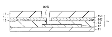
図1は、本技術の一実施の形態に係る半導体装置(半導体装置1)の断面構成を模式的に表したものである。半導体装置1は、例えば表示装置および撮像装置(後述の図7の表示装置2Aおよび図8の撮像装置2B)等の駆動回路に用いられるものである。この半導体装置1には、トップゲート型の薄膜トランジスタ(トランジスタTr)および保持容量(保持容量Cs)が設けられ、トランジスタTrと保持容量Csとが電気的に接続されている。
<Embodiment>
[Constitution]
FIG. 1 schematically shows a cross-sectional configuration of a semiconductor device (semiconductor device 1) according to an embodiment of the present technology. The semiconductor device 1 is used in a drive circuit of, for example, a display device and an image pickup device (
トランジスタTrは、基板11上に、第1絶縁膜13を介して半導体補助膜14、半導体膜15、第2絶縁膜16およびゲート電極17をこの順に有している。半導体膜15(後述の低抵抗領域15b)には接続配線17Aを介してソース・ドレイン電極21Aが電気的に接続されている。ここで、半導体補助膜14が、本技術の第1半導体補助膜の一具体例に対応し、第2絶縁膜16が、本技術のゲート絶縁膜の一具体例に対応する。
The transistor Tr has a semiconductor
保持容量Csは、基板11上に、第1電極12、第1絶縁膜13、半導体補助膜14Cおよび第2電極15Cをこの順に有している。トランジスタTrの半導体膜15が、接続配線17Bにより、保持容量Csの第1電極12に電気的に接続されている。接続配線17Bと第2電極15Cとの間には、第2絶縁膜16が設けられている。第2絶縁膜16には、第2絶縁膜16を貫通する孔部16HA,16HB,16HCが設けられている。接続配線17Aは孔部16HAを覆い、接続配線17Bは孔部16HBを覆い、接続配線17Cは孔部16HCを覆っている。ここで、半導体補助膜14Cが、本技術の第2半導体補助膜の一具体例に対応する。
The holding capacity Cs has a
半導体装置1には、ゲート電極17および接続配線17A,17B,17Cを覆うパッシベーション膜18および層間絶縁膜19が設けられている。層間絶縁膜19は、パッシベーション膜18を間にしてゲート電極17および接続配線17A,17B,17Cを覆っている。ソース・ドレイン電極21Aは、層間絶縁膜19上に設けられており、層間絶縁膜19およびパッシベーション膜18を貫通する接続孔HAを介して接続配線17Aに接続されている。半導体装置1は、例えば、層間絶縁膜19上に、ソース・ドレイン電極21Aとともに、配線21B,21Cを有している。配線21B,21Cは各々、層間絶縁膜19およびパッシベーション膜18を貫通する接続孔HB,HCを介して接続配線17B,17Cに接続されている。
The semiconductor device 1 is provided with a
半導体膜15のうち、ゲート電極17と対向する領域は、トランジスタTrのチャネル領域15aであり、このチャネル領域15aに隣接してチャネル領域15aよりも電気抵抗の低い低抵抗領域15bが設けられている。
The region of the
基板11は、例えば、ガラス,石英およびシリコンなどから構成されている。あるいは、基板11は、例えば、PET(ポリエチレンテレフタレート),PI(ポリイミド),PC(ポリカーボネート)またはPEN(ポリエチレンナフタレート)などの樹脂材料から構成されていてもよい。この他にも、ステンレス鋼(SUS)などの金属板に絶縁材料を成膜したものを基板11に用いることもできる。
The
基板11と第1電極12との間、および基板11と第1絶縁膜13との間には、UC(Under Coat)膜を設けるようにしてもよい(図示せず)。UC膜は、基板11から、上層に例えばナトリウムイオン等の物質が移動するのを防ぐためのものであり、窒化シリコン(SiN)膜および酸化シリコン(SiO)膜等の絶縁材料により構成されている。例えば、UC膜は、基板11側から順に窒化シリコン(SiN)膜および酸化シリコン(SiO)膜を含む積層膜により構成されている。
A UC (Under Coat) film may be provided between the
(保持容量Cs)
第1電極12は、基板11上の選択的な領域に設けられている。第1電極12は、第2電極15Cに対向する部分と、第2電極15Cに非対向の部分とを含んでいる。第1電極12のうち、第2電極15Cに非対向の部分は、第2電極15CよりもトランジスタTr側(図1のX軸方向)に設けられており、孔部16HBに対向している。第1電極12は、例えば、モリブデン(Mo),タングステン(W),アルミニウム(Al),銅(Cu),銀(Ag)およびチタン(Ti)等の金属を含んで構成されている。第1電極12は、合金により構成されていてもよく、複数の金属膜を含む積層膜により構成されていてもよい。第1電極12は、金属以外の導電性材料により構成されていてもよい。
(Retention capacity Cs)
The
第1絶縁膜13は、第1電極12と半導体補助膜14Cとの間に介在している。第1絶縁膜13には、第1絶縁膜13を貫通して第1電極12に達する孔部13Hが設けられている。この孔部13Hは、孔部16HBに対向する位置に設けられている。接続配線17Bは、孔部16HBおよび孔部13Hを介して第1電極12に接続されている。第1絶縁膜13は、例えばシリコン酸化膜(SiOx)、シリコン窒化膜(SiNx)、酸窒化シリコン(SiON)および酸化アルミニウム膜(AlOx)等の無機絶縁膜により構成されている。
The first insulating
第2電極15Cは、第1絶縁膜13および半導体補助膜14Cを間にして第1電極12に対向している。第2電極15Cは、第1電極12に対向する部分と、第1電極12に非対向の部分とを含んでいる。第2電極15Cのうち、第1電極12に非対向の部分は、第1電極12に対向する部分からトランジスタTrと反対側(図1のX軸方向)に延在して設けられている。後述するように、この第2電極15Cは、例えば半導体膜15と同一工程で形成されるものであり、半導体膜15と同一の材料により構成されている。第2電極15Cは、例えば酸化物半導体材料により構成されている。
The
第1絶縁膜13と第2電極15Cとの間に設けられた半導体補助膜14Cは、平面(図1のXY平面)視で第2電極15Cに重なる領域に設けられている。換言すれば、平面視で、第2電極15Cの端面と略同じ位置に、半導体補助膜14Cの端面が配置されている。半導体補助膜14Cは、第2電極15Cの下面(基板11側の面)に接している。後述するように、この半導体補助膜14Cは、例えば半導体補助膜14と同一工程で形成されるものであり、半導体補助膜14と同一の材料により構成されている。
The semiconductor auxiliary film 14C provided between the first insulating
この半導体補助膜14Cは、例えば、酸化物半導体からなる第2電極15Cに接することにより、第2電極15Cの電気抵抗を下げる、即ち、低抵抗化させる役割を担っている。具体的には、半導体補助膜14Cは、例えば、酸化物半導体材料に対してキャリア供与性を有しており、酸化物半導体材料にキャリアを供給するようになっている。これにより、酸化物半導体材料の導電性が高まり、酸化物半導体材料からなる第2電極15Cを低抵抗化することができる。あるいは、半導体補助膜14Cは導電性を有していてもよい。これにより、半導体補助膜14C自身が、第2電極15Cとともに保持容量Csを構成する一対の電極の一方として機能するようになる。
The semiconductor auxiliary film 14C plays a role of lowering the electrical resistance of the
第2電極15C上の第2絶縁膜16は、第2電極15Cの上面を覆うとともに、第2電極15Cおよび半導体補助膜14Cの端面を覆っている。第2絶縁膜16には、第2絶縁膜16を貫通して第2電極15Cに達する孔部16HCが設けられている。例えば、この孔部16HCを埋め込むように接続配線17Cが設けられ、これにより、接続配線17Cが第2電極15Cに電気的に接続されている。第2絶縁膜16の孔部16HBは、第1電極12に対向する位置に配置されている。この孔部16HBの側壁の一部は、第1絶縁膜13の孔部13Hの側壁の一部と、平面視で略同じ位置に配置されており、孔部16HBは孔部13Hに連通している。孔部16HBおよび孔部13Hに埋設された接続配線17Bが第1電極12に接続されている。
The second insulating
(トランジスタTr)
図2(A)(B)は、トランジスタTrの構成を模式的に表している。図2(A)は、トランジスタTrの断面構成を表し、図2(B)は、トランジスタTrの平面構成を表している。
(Transistor Tr)
2 (A) and 2 (B) schematically show the configuration of the transistor Tr. FIG. 2A shows a cross-sectional structure of the transistor Tr, and FIG. 2B shows a planar structure of the transistor Tr.
半導体膜15は、第1絶縁膜13上の選択的な領域に設けられている。半導体膜15は、例えば、インジウム(In),ガリウム(Ga),亜鉛(Zn),スズ(Sn),チタン(Ti)およびニオブ(Nb)のうちの少なくとも1種の元素の酸化物を主成分として含む酸化物半導体から構成されている。具体的には、半導体膜15に酸化インジウムスズ亜鉛(ITZO),酸化インジウムガリウム亜鉛(IGZO:InGaZnO),酸化亜鉛(ZnO),酸化インジウム亜鉛(IZO),酸化インジウムガリウム(IGO),酸化インジウムスズ(ITO)および酸化インジウム(InO)等を用いることができる。半導体膜15は、アモルファスシリコン,微結晶シリコン,多結晶シリコンまたは有機半導体等の他の半導体材料を用いて構成するようにしてもよい。半導体膜15の厚みは、例えば10nm〜300nmであり、60nm以下であることが好ましい。半導体膜15の厚みを薄くすることにより、半導体中に含まれる欠陥の絶対量が減少し、しきい値電圧の負シフトが抑えられる。したがって、オンオフ比の高い、優れたトランジスタ特性を実現することができる。また、半導体膜15の成膜に要する時間が短縮されるので、生産性を向上させることができる。
The
半導体膜15は、チャネル領域15aの両側に一対の低抵抗領域15bを有している。一方の低抵抗領域15bには、接続配線17Aを介してソース・ドレイン電極21Aが接続されている。他方の低抵抗領域15b(保持容量Cs側の低抵抗領域15b)は、チャネル領域15aに隣接する位置から第2絶縁膜16と第2絶縁膜16との孔部16HBに対向する位置まで延在しており、接続配線17Bを介して保持容量Csの第1電極12に接続されている。
The
第1絶縁膜13と半導体膜15との間に設けられた半導体補助膜14は、基板11上の選択的な領域に設けられている。具体的には、平面視で半導体膜15の一対の低抵抗領域15b各々に重なる領域に、一対の半導体補助膜14が設けられている。この一対の半導体補助膜14は各々、半導体膜15の下面に接している。平面視で半導体膜15のチャネル領域15aに重なる領域には、半導体補助膜14は設けられていない。即ち、一対の半導体補助膜14は各々、半導体膜15のチャネル領域15aおよび低抵抗領域15bのうち、低抵抗領域15bに選択的に接している。一対の半導体補助膜14の外側の端面は、平面視で、半導体膜15の端面E15と略同じ位置に配置されている。即ち、低抵抗領域15bの半導体膜15の下面略全面に接するように、半導体補助膜14が設けられている。
The
この一対の半導体補助膜14は、半導体膜15に一対の低抵抗領域15bを形成するためのものである。換言すれば、一対の半導体補助膜14により、半導体膜15の一対の低抵抗領域15bが規定されている。半導体補助膜14が半導体膜15に接することにより、低抵抗領域15bを介した電流の流れが促されるようになっている。
The pair of semiconductor
例えば、半導体補助膜14は、半導体膜15の低抵抗領域15bに選択的に接することにより、低抵抗領域15bの電気抵抗を下げる、即ち、低抵抗化させる役割を担っている。具体的には、半導体補助膜14は、例えば、半導体膜15に対してキャリア供与性を有しており、低抵抗領域15bにキャリアを供給するようになっている。これにより、低抵抗領域15bの導電性が高まり、低抵抗領域15bを低抵抗化することができる。このようなキャリア供与性を有する半導体補助膜14,14Cは、例えば、アルミニウム(Al)等の金属を含んでいる。具体的には、半導体補助膜14,14Cとして、アルミニウム(Al)の単体およびアルミニウムを含む合金等を用いることができる。アルミニウムを含む合金としては、例えば、AlSi(アルミニウムシリコン合金)およびAlCu(アルミニウム銅合金)等が挙げられる。
For example, the
あるいは、半導体補助膜14は導電性を有していてもよい。これにより、低抵抗領域15bでは、半導体補助膜14自身が導体として機能し、半導体膜15とともに半導体補助膜14を介して電流が流れるようになる。このような導電性を有する半導体補助膜14,14Cには、例えば、インジウム(In)を含む金属酸化物または亜鉛(Zn)を含む金属酸化物等を用いることができる。インジウムを含む金属酸化物としては、例えば、酸化インジウムスズ(ITO:Indium Tin Oxide)および酸化インジウム亜鉛(IZO:Indium Zinc Oxide)等が挙げられる。亜鉛を含む金属酸化物としては、例えば、ZnO(酸化亜鉛)および酸化アルミニウム亜鉛(AZO:Aluminum doped Zinc Oxide)等が挙げられる。
Alternatively, the
半導体補助膜14,14Cの厚みは、例えば2nm〜300nm程度である。このようなキャリア供与性または導電性を有する半導体補助膜14を設けることにより、低抵抗領域15bを介した電流の流れが促進される。また、仮に、第2絶縁膜16に、孔部(後述の孔部16HA)を形成する際に、半導体膜15がオーバーエッチングされても、半導体補助膜14が設けられていることにより、低抵抗領域15bでの電気抵抗の上昇が抑えられる。
The thickness of the semiconductor
図3A,図3Bは、一対の半導体補助膜14の内側の端面の配置の一例を表している。一対の半導体補助膜14の内側の端面は、図3Aに示したように、ゲート電極17に対向する位置に配置されていてもよい。一対の半導体補助膜14の内側の端面は、図3Bに示したように、ゲート電極17に非対向の位置に配置されていてもよい。平面視での、ゲート電極17の端面から一対の半導体補助膜14各々の内側の端面までのチャネル長方向(図3A,図3BのX軸方向)の距離Dは、0.5μm〜3μm程度であることが好ましい。ゲート電極17に対向する半導体補助膜14の部分が大きくなると(図3A参照)、ゲート電極17と半導体補助膜14との間の寄生容量が大きくなり、トランジスタTrの特性を低下させるおそれがある。また、チャネル領域15a以外の部分の半導体膜15について、半導体補助膜14が積層されていない部分が大きくなると(図3B参照)、半導体膜15に、十分な低抵抗領域15bが形成されず、断線等の不具合が発生するおそれがある。
3A and 3B show an example of the arrangement of the inner end faces of the pair of semiconductor
半導体膜15とゲート電極17との間には、第2絶縁膜16が設けられている。この第2絶縁膜16は、トランジスタTrのゲート絶縁膜として機能する。本実施の形態では、この第2絶縁膜16が、半導体膜15のチャネル領域15aから低抵抗領域15bの少なくとも一部までを覆っている。したがって、半導体膜15のチャネル領域15aおよび低抵抗領域15bのうち、チャネル領域15aに対向するゲート電極17近傍には、第2絶縁膜16の端面(後述の図6の端面E116)が形成されない。詳細は後述するが、これにより、第2絶縁膜16の端面の付着物を介した半導体膜15とゲート電極17との短絡の発生を抑えることができる。
A second insulating
第2絶縁膜16は、例えば、孔部16HA,16HBを除き、半導体膜15を覆っている。換言すれば、孔部16HA,16HBに対向する部分を除き、半導体膜15は第2絶縁膜16に覆われている。例えば、第2絶縁膜16は、孔部16HA,16HBを除き、半導体膜15の全部を覆っているが、第2絶縁膜16は、半導体膜15のうち、チャネル領域15aから低抵抗領域15bの少なくとも一部を覆っていればよい。
The second insulating
孔部16HAは、一方の低抵抗領域15bに対向する位置に設けられ、半導体膜15に達している。孔部16HBは、他方の低抵抗領域15bに対向する位置に設けられ、半導体膜15に達している。換言すれば、孔部16HA,16HBは各々、半導体補助膜14に対向する位置に設けられている。孔部16HAの底面の半導体膜15(低抵抗領域15b)には接続配線17Aが接している。この第2絶縁膜16の孔部16HAを介して、接続配線17Aが半導体膜15の低抵抗領域15bに接続されている。ここで、孔部16HAが、本開示の孔部の一具体例に対応する。孔部16HBの底面の半導体膜15(低抵抗領域15b)には接続配線17Bが接している。この第2絶縁膜16の孔部16HBを介して、接続配線17Bが半導体膜15の低抵抗領域15bに接続されている。
The hole portion 16HA is provided at a position facing one of the
第2絶縁膜16は、例えばシリコン酸化膜(SiOx)、シリコン窒化膜(SiNx)、シリコン窒化酸化膜(SiON)および酸化アルミニウム膜(AlOx)のうちの1種よりなる単層膜、またはそれらのうちの2種以上よりなる積層膜により構成されている。
The second insulating
第2絶縁膜16上の選択的な領域、即ち、チャネル領域15aに対向する領域に設けられたゲート電極17は、印加されるゲート電圧(Vg)によってチャネル領域15a中のキャリア密度を制御すると共に、電位を供給する配線としての機能を有するものである。ゲート電極17は、このゲート電極17の構成材料は、例えば、チタン(Ti),タングステン(W),タンタル(Ta),アルミニウム(Al),モリブデン(Mo),銀(Ag),ネオジウム(Nd)および銅(Cu)のうちの1種を含む単体および合金が挙げられる。あるいは、それらのうちの少なくとも1種を含む化合物および2種以上を含む積層膜であってもよい。また、例えばITO等の透明導電膜が用いられても構わない。
The
第2絶縁膜16の孔部16HAには、接続配線17Aが埋設されている。この接続配線17Aは、層間絶縁膜19上のソース・ドレイン電極21Aと半導体膜15の低抵抗領域15bとを電気的に接続するためのものである。
A
第2絶縁膜16上に設けられた接続配線17B,17Cは、互いに電気的に分離されている。接続配線17Bは、第2絶縁膜16上から孔部16HBおよび第1絶縁膜13の孔部13Hを埋め込むように設けられている。この接続配線17Bにより、半導体膜15の低抵抗領域15bと第1電極12とが電気的に接続されるとともに、第1電極12と層間絶縁膜19上の配線21Bとが電気的に接続される。接続配線17Cは、第2絶縁膜16上から第2絶縁膜16の孔部16HCを埋め込むように設けられている。この接続配線17Cにより、層間絶縁膜19上の配線21Cと第2電極15Cとが電気的に接続される。後述するように、接続配線17A,17B,17Cは、例えばゲート電極17と同一工程で形成されるものであり、ゲート電極17と同一の材料により構成されている。
The connection wirings 17B and 17C provided on the second insulating
パッシベーション膜18は、例えば、ゲート電極17および接続配線17A,17B,17Cを覆うように、基板11の全面に設けられている。このパッシベーション膜18には、例えば、酸化シリコン(SiO2)膜を用いることができる。パッシベーション膜18には、窒化シリコン(SiN)膜または酸窒化シリコン(SiON)膜等を用いるようにしてもよい。
The
層間絶縁膜19は、パッシベーション膜18を間にして、ゲート電極17および接続配線17A,17B,17Cを覆っている。この層間絶縁膜19は、例えば、基板11の全面に設けられている。接続孔HAは、層間絶縁膜19およびパッシベーション膜18を貫通して接続配線17Aに達している。接続孔HAは、例えば、第2絶縁膜16の孔部16HAに対向する位置に設けられている。接続孔HBは、層間絶縁膜19およびパッシベーション膜18を貫通して接続配線17Bに達している。接続孔HBは、例えば、第1絶縁膜13の孔部13Hと非対向の位置に設けられている。接続孔HBは、平面視で、第1絶縁膜13の孔部13HよりもトランジスタTrから離れた位置に設けられている。接続孔HCは、層間絶縁膜19およびパッシベーション膜18を貫通して接続配線17Cに達している。接続孔HCは、例えば、第2絶縁膜16の孔部16HCに対向する位置に設けられている。層間絶縁膜19には、例えば感光性を有する樹脂膜を用いることができる。具体的には、層間絶縁膜19は、例えばポリイミド樹脂膜により構成されている。層間絶縁膜19には、ノボラック樹脂またはアクリル樹脂等を用いるようにしてもよい。
The
層間絶縁膜19上に設けられたソース・ドレイン電極21Aは、接続孔HAを介して接続配線17Aに接続されている。このソース・ドレイン電極21Aは、トランジスタTrのソースまたはドレインとして機能するものであり、例えば、上記ゲート電極17の構成材料として列挙したものと同様の金属または透明導電膜を含んで構成されている。このソース・ドレイン電極としては、電気伝導性の良い材料が選択されることが望ましい。
The source /
層間絶縁膜19上には、ソース・ドレイン電極21Aとともに配線21B,21Cが設けられている。配線21Bは、接続孔HBを介して接続配線21Bに接続されており、配線21Cは、接続孔HCを介して接続配線21Cに接続されている。後述するように、配線21B,21Cは、例えばソース・ドレイン電極21Aと同一工程で形成されるものであり、ソース・ドレイン電極21Aと同一の材料により構成されている。
Wiring 21B and 21C are provided on the
[製造方法]
上記のような半導体装置1は、例えば次のようにして製造することができる(図4A〜図4F)。
[Production method]
The semiconductor device 1 as described above can be manufactured, for example, as follows (FIGS. 4A to 4F).
まず、図4Aに示したように、基板11上に、第1電極12を形成する。第1電極12は、例えば、基板11上の全面に導電性の金属膜を成膜した後、この金属膜をドライエッチングにより所定の形状にパターニングして形成する。
First, as shown in FIG. 4A, the
続いて、図4Bに示したように、第1電極12上の第1絶縁膜13および半導体補助材料膜14Mをこの順に形成する。半導体補助材料膜14Mにより、後の工程で、半導体補助膜14,14Cが形成される。第1絶縁膜13は、第1電極12を覆うようにして、基板11の全面に形成する。半導体補助材料膜14Mは、例えば、スパッタ法を用いてIZOを第1絶縁膜13上に成膜することにより形成する。このとき、後の工程で形成される半導体膜15のチャネル領域15aに対向する部分の半導体材料膜14Mは、例えば、フォトリソグラフィおよびウェットエッチングを用いて除去しておく。
Subsequently, as shown in FIG. 4B, the first insulating
半導体補助材料膜14Mを形成した後、図4Cに示したように、半導体膜15および第2電極15Cを形成する。半導体膜15および第2電極15Cは、半導体補助材料膜14M上に、酸化物半導体材料を例えばスパッタ法等により成膜した後、例えばフォトリソグラフィおよびウェットエッチングを用いて、これを所定の形状にパターニングして形成する。この酸化物半導体材料のパターニングと連続して、半導体補助材料膜14Mをパターニングする。これにより、半導体膜15の直下に一対の半導体補助膜14が形成されるとともに、第2電極15Cの直下に半導体補助膜14Cが形成される。この一対の半導体補助膜14により、半導体膜15には、一対の低抵抗領域15bが形成される。
After forming the semiconductor
次に、図4Dに示したように、半導体膜15および第2電極15Cを覆うようにして基板11の全面に第2絶縁膜16を形成する。第2絶縁膜16は、例えば、基板11の全面に例えばCVD(Chemical Vapor Deposition)法を用いて酸化シリコン(SiO)等の絶縁膜を成膜することにより形成する。この後、この絶縁膜に、フォトリソグラフィおよびドライエッチングを用いて孔部16HBを形成する。これにより、孔部16HBとともに、孔部16HBに対向する位置の第1絶縁膜13に孔部13Hが形成される。孔部16HBを形成した後、第2絶縁膜16には孔部16HA,16HCを形成しておく。
Next, as shown in FIG. 4D, the second insulating
続いて、図4Eに示したように、第2絶縁膜16上にゲート電極17および接続配線17A,17B,17Cを形成する。ゲート電極17および接続配線17A,17B,17Cは、例えば、以下のようにして形成する。まず、第2絶縁膜16を覆うように、基板11の全面に導電性の金属材料を成膜する。次に、この金属膜をフォトリソグラフィおよびドライエッチングを用いて所定の形状にパターニングする。これにより、一対の半導体補助膜14に非対向の領域にゲート電極17を形成するとともに、孔部16HAを埋める接続配線17A、孔部16HBを埋める接続配線17Bおよび孔部16HCを埋める接続配線17Cを形成することができる。
Subsequently, as shown in FIG. 4E, the
この後、図4Fに示したように、基板11の全面に、パッシベーション膜18および層間絶縁膜19を形成する。パッシベーション膜18および層間絶縁膜19には、接続孔HA,HB,HCを形成しておく。最後に、層間絶縁膜19上に、ソース・ドレイン電極21Aおよび配線21B,21Cを形成することにより、図1に示した半導体装置1が完成する。
After that, as shown in FIG. 4F, the
[作用、効果]
本実施の形態の半導体装置1では、ゲート電極17に閾値電圧以上のオン電圧が印加されると、半導体膜15のチャネル領域15aが活性化される。これにより、一対の低抵抗領域15b間に電流が流れる。これに応じて、接続配線17Bを介して、半導体膜15から第1電極12に電流が流れ保持容量Csに電荷が保持される。
[Action, effect]
In the semiconductor device 1 of the present embodiment, when an on-voltage equal to or higher than the threshold voltage is applied to the
本実施の形態の半導体装置1では、第2絶縁膜16が、半導体膜15のチャネル領域15aから一対の低抵抗領域15bの端部近傍までを覆っている。これにより、第2絶縁膜16の端面の付着物を介したゲート電極17と半導体膜15との間の短絡の発生が抑えられる。以下、この作用効果について、比較例を用いて説明する。
In the semiconductor device 1 of the present embodiment, the second insulating
図5は、比較例にかかる半導体装置(半導体装置100)の要部の模式的な断面構成を表したものである。この半導体装置100は、いわゆるセルフアライン構造のトランジスタTrを有している。具体的には、ゲート絶縁膜(ゲート絶縁膜116)が、ゲート電極17と略同じ平面形状を有しており、平面視で、ゲート電極17の端面と略同じ位置に、ゲート絶縁膜116の端面(後述の図6の端面E116)が設けられている。即ち、ゲート絶縁膜116は、半導体膜15のうち、チャネル領域15aのみを覆っている。
FIG. 5 shows a schematic cross-sectional configuration of a main part of the semiconductor device (semiconductor device 100) according to the comparative example. The
また、半導体装置100は、半導体膜15の低抵抗領域15bに接する金属酸化膜118を有している。金属酸化膜118は、例えば酸化アルミニウム(AlO)等により構成されている。この金属酸化膜118は、半導体膜15から酸素を引き抜くことにより、半導体膜15を低抵抗化する役割を担っている。このような金属酸化膜118を設けることにより、半導体装置100では、一対の半導体補助膜14とゲート電極17との間に合わせずれが生じても、半導体膜15のチャネル領域15aに隣接する位置に、低抵抗領域15bが形成されるようになっている。
Further, the
しかし、このような半導体装置100では、ゲート絶縁膜116の端面の付着物(後述の図6の付着物115)に起因して、ゲート電極17と半導体膜15との間に短絡が発生するおそれがある。
However, in such a
図6は、図5に示した部分Rの拡大図である。ゲート絶縁膜116は、ゲート電極17を形成した後、このゲート電極17の形状に対応させて絶縁膜をパターニングすることにより形成されている。この絶縁膜をパターニングする際のドライエッチングで、オーバーエッチングが行われると、半導体膜15が逆スパッタされ、ゲート絶縁膜116の端面E116に半導体膜15に起因した付着物115が設けられる。この付着物115により、ゲート電極17および半導体膜15の耐圧性が低下し、これらの間で短絡が発生するおそれがある。この短絡に起因して半導体装置100では、不具合が発生しやすくなる。
FIG. 6 is an enlarged view of the portion R shown in FIG. The
これに対し、半導体装置1では、第2絶縁膜16が、半導体膜15のチャネル領域15aおよび一対の低抵抗領域15bを覆っている。このため、第2絶縁膜16の端面は、チャネル長方向において、ゲート電極17から離間した位置に形成される。したがって、第2絶縁膜16の端面の付着物(図6の付着物115)を介したゲート電極17と半導体膜15との間の短絡の発生が抑えられる。
On the other hand, in the semiconductor device 1, the second insulating
また、半導体装置1では、ゲート電極17の形状に対応させて第2絶縁膜16をパターニングする工程が不要となるので、半導体装置100に比べてタクトタイムを短縮することが可能となる。
Further, in the semiconductor device 1, the step of patterning the second insulating
また、半導体装置1では、半導体膜15の一対の低抵抗領域15bが、一対の半導体補助膜14により形成されるので、金属酸化膜(半導体装置100の金属酸化膜118)が不要となる。このため、半導体装置100に比べてコストを抑えることが可能となる。
Further, in the semiconductor device 1, since the pair of
以上説明したように本実施の形態では、第2絶縁膜16が、半導体膜15のチャネル領域15aから低抵抗領域15bの少なくとも一部まで覆うようにしたので、第2絶縁膜16の端面の付着物を介したゲート電極17と半導体膜15との間の短絡の発生を抑えることができる。よって、短絡の発生に起因した不具合の発生を抑えることが可能となる。
As described above, in the present embodiment, the second insulating
<適用例1>
上記実施の形態において説明した半導体装置1は、例えば表示装置(後述の図7の表示装置2A)および撮像装置(後述の図8の撮像装置2B)等の駆動回路に用いることができる。
<Application example 1>
The semiconductor device 1 described in the above embodiment can be used for a drive circuit of, for example, a display device (
図7は、表示装置2Aの機能ブロック構成を示したものである。表示装置2Aは、外部から入力された映像信号あるいは内部で生成した映像信号を、映像として表示するものであり、上述した有機ELディスプレイの他にも、例えば液晶ディスプレイなどにも適用される。表示装置2Aは、例えばタイミング制御部31と、信号処理部32と、駆動部33と、表示画素部34とを備えている。
FIG. 7 shows the functional block configuration of the
タイミング制御部31は、各種のタイミング信号(制御信号)を生成するタイミングジェネレータを有しており、これらの各種のタイミング信号を基に、信号処理部32等の駆動制御を行うものである。信号処理部32は、例えば、外部から入力されたデジタルの映像信号に対して所定の補正を行い、それにより得られた映像信号を駆動部33に出力するものである。駆動部33は、例えば走査線駆動回路および信号線駆動回路などを含んで構成され、各種制御線を介して表示画素部34の各画素を駆動するものである。表示画素部34は、例えば有機EL素子または液晶表示素子等の表示素子と、表示素子を画素毎に駆動するための画素回路とを含んで構成されている。これらのうち、例えば、駆動部33または表示画素部34の一部を構成する各種回路に、上述の半導体装置1が用いられる。
The
図8は、撮像装置2Bの機能ブロック構成を示したものである。撮像装置2Bは、例えば画像を電気信号として取得する固体撮像装置であり、例えばCCD(Charge Coupled Device)またはCMOS(Complementary Metal Oxide Semiconductor)イメージセンサなどから構成されている。撮像装置2Bは、例えばタイミング制御部35と、駆動部36と、撮像画素部37と、信号処理部38とを備えている。
FIG. 8 shows the functional block configuration of the
タイミング制御部35は、各種のタイミング信号(制御信号)を生成するタイミングジェネレータを有しており、これらの各種のタイミング信号を基に、駆動部36の駆動制御を行うものである。駆動部36は、例えば行選択回路、AD変換回路および水平転送走査回路などを含んで構成され、各種制御線を介して撮像画素部37の各画素から信号を読み出す駆動を行うものである。撮像画素部37は、例えばフォトダイオードなどの撮像素子(光電変換素子)と、信号読み出しのための画素回路とを含んで構成されている。信号処理部38は、撮像画素部37から得られた信号に対して様々な信号処理を施すものである。これらのうち、例えば、駆動部36または撮像画素部37の一部を構成する各種回路に、上述の半導体装置1が用いられる。
The
<電子機器の例>
上記表示装置2Aおよび撮像装置2B等は、様々なタイプの電子機器に用いることができる。図9に、電子機器3の機能ブロック構成を示す。電子機器3としては、例えばテレビジョン装置、パーソナルコンピュータ(PC)、スマートフォン、タブレット型PC、携帯電話機、デジタルスチルカメラおよびデジタルビデオカメラ等が挙げられる。
<Example of electronic device>
The
電子機器3は、例えば上述の表示装置2A(または撮像装置2B)と、インターフェース部40とを有している。インターフェース部40は、外部から各種の信号および電源等が入力される入力部である。このインターフェース部40は、また、例えばタッチパネル、キーボードまたは操作ボタン等のユーザインターフェースを含んでいてもよい。
The electronic device 3 has, for example, the above-mentioned
以上、実施の形態を挙げて説明したが、本技術は上記実施の形態に限定されるものではなく、種々変形が可能である。例えば、上記実施の形態に記載した各層の材料および厚みは列挙したものに限定されるものではなく、他の材料および厚みとしてもよい。 Although the embodiments have been described above, the present technology is not limited to the above embodiments and can be modified in various ways. For example, the material and thickness of each layer described in the above embodiment are not limited to those listed, and may be other materials and thickness.
また、上記実施の形態では、半導体補助膜14,14Cが半導体膜15,第2電極15Cの下面に接する場合について説明したが、半導体補助膜14,14Cは半導体膜15,第2電極15Cの上面に接していてもよい。
Further, in the above embodiment, the case where the semiconductor
また、上記実施の形態では、トランジスタTrおよび保持容量Csを含む半導体装置1を例に挙げて説明したが、半導体装置1は、少なくともトランジスタTrを有していればよい。 Further, in the above embodiment, the semiconductor device 1 including the transistor Tr and the holding capacitance Cs has been described as an example, but the semiconductor device 1 may have at least the transistor Tr.
上記実施の形態等において説明した効果は一例であり、本開示の効果は、他の効果であってもよいし、更に他の効果を含んでいてもよい。 The effects described in the above embodiments and the like are examples, and the effects of the present disclosure may be other effects or may further include other effects.
尚、本技術は以下のような構成を取ることも可能である。
(1)
基板と、
前記基板上の選択的な領域に設けられた第1半導体補助膜と、
酸化物半導体材料を含むともに、前記第1半導体補助膜に接する低抵抗領域と、前記低抵抗領域と異なる部分に設けられたチャネル領域とを有する半導体膜と、
前記半導体膜を前記チャネル領域から前記低抵抗領域の少なくとも一部まで覆うゲート絶縁膜と、
前記ゲート絶縁膜を間にして前記半導体膜の前記チャネル領域に対向するゲート電極と
を備えた半導体装置。
(2)
前記第1半導体補助膜は、前記半導体膜の前記低抵抗領域を介した電流の流れを促す
前記(1)に記載の半導体装置。
(3)
更に、前記半導体膜の前記低抵抗領域に対向する位置に設けられるとともに、前記ゲート絶縁膜を貫通する孔部と、
前記孔部を介して前記半導体膜の前記低抵抗領域に電気的に接続されたソース・ドレイン電極とを有する
前記(1)または(2)に記載の半導体装置。
(4)
前記基板上に、前記第1半導体補助膜、前記半導体膜、前記ゲート絶縁膜、前記ゲート電極および前記ソース・ドレイン電極の順に設けられている
前記(3)に記載の半導体装置。
(5)
前記第1半導体補助膜は金属を含む
前記(1)ないし(4)のうちいずれか1つに記載の半導体装置。
(6)
前記第1半導体補助膜はアルミニウムを含む
前記(1)ないし(5)のうちいずれか1つに記載の半導体装置。
(7)
前記第1半導体補助膜は金属酸化物を含む
前記(1)ないし(4)のうちいずれか1つに記載の半導体装置。
(8)
前記第1半導体補助膜は、酸化インジウムスズ(Indium Tin Oxide)または酸化インジウム亜鉛(Indium Zinc Oxide)を含む
前記(1)ないし(4)のうちいずれか1つに記載の半導体装置。
(9)
更に、
前記基板上に設けられるとともに、前記半導体膜の前記低抵抗領域に電気的に接続された第1電極と、
前記酸化物半導体材料を含むとともに、前記第1電極の少なくとも一部に対向して設けられた第2電極と、
前記第1半導体補助膜の構成材料と同じ材料を含むとともに、前記第2電極に接する第2半導体補助膜とを有する
前記(1)ないし(8)のうちいずれか1つ記載の半導体装置。
(10)
前記基板上に、前記第1電極、前記第2半導体補助膜および前記第2電極の順に設けられている
前記(9)に記載の半導体装置。
(11)
表示素子および前記表示素子を駆動する半導体装置を備え、
前記半導体装置は、
基板と、
前記基板上の選択的な領域に設けられた第1半導体補助膜と、
酸化物半導体材料を含むともに、前記第1半導体補助膜に接する低抵抗領域と、前記低抵抗領域と異なる部分に設けられたチャネル領域とを有する半導体膜と、
前記半導体膜を前記チャネル領域から前記低抵抗領域の少なくとも一部まで覆うゲート絶縁膜と、
前記ゲート絶縁膜を間にして前記半導体膜の前記チャネル領域に対向するゲート電極とを含む
表示装置。
The present technology can also have the following configurations.
(1)
With the board
A first semiconductor auxiliary film provided in a selective region on the substrate,
A semiconductor film containing an oxide semiconductor material and having a low resistance region in contact with the first semiconductor auxiliary film and a channel region provided in a portion different from the low resistance region.
A gate insulating film that covers the semiconductor film from the channel region to at least a part of the low resistance region.
A semiconductor device including a gate electrode facing the channel region of the semiconductor film with the gate insulating film in between.
(2)
The semiconductor device according to (1), wherein the first semiconductor auxiliary film promotes the flow of an electric current through the low resistance region of the semiconductor film.
(3)
Further, a hole portion that is provided at a position facing the low resistance region of the semiconductor film and that penetrates the gate insulating film, and
The semiconductor device according to (1) or (2) above, which has a source / drain electrode electrically connected to the low resistance region of the semiconductor film via the hole.
(4)
The semiconductor device according to (3), wherein the first semiconductor auxiliary film, the semiconductor film, the gate insulating film, the gate electrode, and the source / drain electrode are provided in this order on the substrate.
(5)
The semiconductor device according to any one of (1) to (4) above, wherein the first semiconductor auxiliary film contains a metal.
(6)
The semiconductor device according to any one of (1) to (5) above, wherein the first semiconductor auxiliary film contains aluminum.
(7)
The semiconductor device according to any one of (1) to (4) above, wherein the first semiconductor auxiliary film contains a metal oxide.
(8)
The semiconductor device according to any one of (1) to (4) above, wherein the first semiconductor auxiliary film contains indium tin oxide (Indium Tin Oxide) or indium zinc oxide (Indium Zinc Oxide).
(9)
In addition
A first electrode provided on the substrate and electrically connected to the low resistance region of the semiconductor film,
A second electrode containing the oxide semiconductor material and provided so as to face at least a part of the first electrode.
The semiconductor device according to any one of (1) to (8), which contains the same material as the constituent material of the first semiconductor auxiliary film and has a second semiconductor auxiliary film in contact with the second electrode.
(10)
The semiconductor device according to (9), wherein the first electrode, the second semiconductor auxiliary film, and the second electrode are provided on the substrate in this order.
(11)
A display element and a semiconductor device for driving the display element are provided.
The semiconductor device is
With the board
A first semiconductor auxiliary film provided in a selective region on the substrate,
A semiconductor film containing an oxide semiconductor material and having a low resistance region in contact with the first semiconductor auxiliary film and a channel region provided in a portion different from the low resistance region.
A gate insulating film that covers the semiconductor film from the channel region to at least a part of the low resistance region.
A display device including a gate electrode having a gate insulating film in between and facing the channel region of the semiconductor film.
1…半導体装置、Tr…トランジスタ、Cs…保持容量、11…基板、12…第1電極、13…第1絶縁膜、14,14C…第1絶縁膜、15…半導体膜、15a…チャネル領域、15b…低抵抗領域、15C…第2電極、16…第2絶縁膜16…第2絶縁膜、17…ゲート電極、17A,17B,17C…接続配線、18…パッシベーション膜、19…層間絶縁膜、21A…ソース・ドレイン電極、21B,21C…配線、2A…表示装置、2B…撮像装置、3…電子機器、31,35…タイミング制御部、32,38…信号処理部、33,36…駆動部、34…表示画素部、37…撮像画素部、40…インターフェース部、13H,16H,16CH…孔部、S…間隙、E15,E16,E16C…間隙、HA,HB,HC…接続孔。
1 ... Semiconductor device, Tr ... Transistor, Cs ... Retention capacity, 11 ... Substrate, 12 ... First electrode, 13 ... First insulating film, 14, 14C ... First insulating film, 15 ... Semiconductor film, 15a ... Channel region, 15b ... low resistance region, 15C ... second electrode, 16 ... second insulating
Claims (11)
前記基板上の選択的な領域に設けられた第1半導体補助膜と、
酸化物半導体材料を含むともに、前記第1半導体補助膜に接する低抵抗領域と、前記低抵抗領域と異なる部分に設けられたチャネル領域とを有する半導体膜と、
前記半導体膜を前記チャネル領域から前記低抵抗領域の少なくとも一部まで覆うゲート絶縁膜と、
前記ゲート絶縁膜を間にして前記半導体膜の前記チャネル領域に対向するゲート電極と
を備えた半導体装置。 With the board
A first semiconductor auxiliary film provided in a selective region on the substrate,
A semiconductor film containing an oxide semiconductor material and having a low resistance region in contact with the first semiconductor auxiliary film and a channel region provided in a portion different from the low resistance region.
A gate insulating film that covers the semiconductor film from the channel region to at least a part of the low resistance region.
A semiconductor device including a gate electrode facing the channel region of the semiconductor film with the gate insulating film in between.
請求項1に記載の半導体装置。 The semiconductor device according to claim 1, wherein the first semiconductor auxiliary film is a semiconductor device that promotes the flow of an electric current through the low resistance region of the semiconductor film.
前記孔部を介して前記半導体膜の前記低抵抗領域に電気的に接続されたソース・ドレイン電極とを有する
請求項1に記載の半導体装置。 Further, a hole portion that is provided at a position facing the low resistance region of the semiconductor film and that penetrates the gate insulating film, and
The semiconductor device according to claim 1, further comprising a source / drain electrode electrically connected to the low resistance region of the semiconductor film via the pore portion.
請求項3に記載の半導体装置。 The semiconductor device according to claim 3, wherein the first semiconductor auxiliary film, the semiconductor film, the gate insulating film, the gate electrode, and the source / drain electrode are provided in this order on the substrate.
請求項1に記載の半導体装置。 The semiconductor device according to claim 1, wherein the first semiconductor auxiliary film contains a metal.
請求項1に記載の半導体装置。 The semiconductor device according to claim 1, wherein the first semiconductor auxiliary film contains aluminum.
請求項1に記載の半導体装置。 The semiconductor device according to claim 1, wherein the first semiconductor auxiliary film contains a metal oxide.
請求項1に記載の半導体装置。 The semiconductor device according to claim 1, wherein the first semiconductor auxiliary film contains indium tin oxide (Indium Tin Oxide) or indium zinc oxide (Indium Zinc Oxide).
前記基板上に設けられるとともに、前記半導体膜の前記低抵抗領域に電気的に接続された第1電極と、
前記酸化物半導体材料を含むとともに、前記第1電極の少なくとも一部に対向して設けられた第2電極と、
前記第1半導体補助膜の構成材料と同じ材料を含むとともに、前記第2電極に接する第2半導体補助膜とを有する
請求項1記載の半導体装置。 In addition
A first electrode provided on the substrate and electrically connected to the low resistance region of the semiconductor film,
A second electrode containing the oxide semiconductor material and provided so as to face at least a part of the first electrode.
The semiconductor device according to claim 1, further comprising the same material as the constituent material of the first semiconductor auxiliary film and having a second semiconductor auxiliary film in contact with the second electrode.
請求項9に記載の半導体装置。 The semiconductor device according to claim 9, wherein the first electrode, the second semiconductor auxiliary film, and the second electrode are provided on the substrate in this order.
前記半導体装置は、
基板と、
前記基板上の選択的な領域に設けられた第1半導体補助膜と、
酸化物半導体材料を含むともに、前記第1半導体補助膜に接する低抵抗領域と、前記低抵抗領域と異なる部分に設けられたチャネル領域とを有する半導体膜と、
前記半導体膜を前記チャネル領域から前記低抵抗領域の少なくとも一部まで覆うゲート絶縁膜と、
前記ゲート絶縁膜を間にして前記半導体膜の前記チャネル領域に対向するゲート電極とを含む
表示装置。 A display element and a semiconductor device for driving the display element are provided.
The semiconductor device is
With the board
A first semiconductor auxiliary film provided in a selective region on the substrate,
A semiconductor film containing an oxide semiconductor material and having a low resistance region in contact with the first semiconductor auxiliary film and a channel region provided in a portion different from the low resistance region.
A gate insulating film that covers the semiconductor film from the channel region to at least a part of the low resistance region.
A display device including a gate electrode having a gate insulating film in between and facing the channel region of the semiconductor film.
Priority Applications (2)
| Application Number | Priority Date | Filing Date | Title |
|---|---|---|---|
| JP2019080382A JP2020178079A (en) | 2019-04-19 | 2019-04-19 | Semiconductor device and display device |
| US16/736,814 US11081591B2 (en) | 2019-04-19 | 2020-01-08 | Semiconductor device and display unit |
Applications Claiming Priority (1)
| Application Number | Priority Date | Filing Date | Title |
|---|---|---|---|
| JP2019080382A JP2020178079A (en) | 2019-04-19 | 2019-04-19 | Semiconductor device and display device |
Publications (2)
| Publication Number | Publication Date |
|---|---|
| JP2020178079A true JP2020178079A (en) | 2020-10-29 |
| JP2020178079A5 JP2020178079A5 (en) | 2021-12-23 |
Family
ID=72831291
Family Applications (1)
| Application Number | Title | Priority Date | Filing Date |
|---|---|---|---|
| JP2019080382A Pending JP2020178079A (en) | 2019-04-19 | 2019-04-19 | Semiconductor device and display device |
Country Status (2)
| Country | Link |
|---|---|
| US (1) | US11081591B2 (en) |
| JP (1) | JP2020178079A (en) |
Citations (3)
| Publication number | Priority date | Publication date | Assignee | Title |
|---|---|---|---|---|
| US20130126868A1 (en) * | 2011-11-18 | 2013-05-23 | Semiconductor Energy Laboratory Co., Ltd. | Semiconductor element, method for manufacturing semiconductor element, and semiconductor device including semiconductor element |
| JP2016057547A (en) * | 2014-09-11 | 2016-04-21 | シャープ株式会社 | Mems display and method for manufacturing the same |
| JP2017228802A (en) * | 2011-04-22 | 2017-12-28 | 株式会社半導体エネルギー研究所 | Semiconductor device |
Family Cites Families (3)
| Publication number | Priority date | Publication date | Assignee | Title |
|---|---|---|---|---|
| CN101263604B (en) | 2005-09-16 | 2012-05-30 | 夏普株式会社 | Thin film transistor |
| WO2015132694A1 (en) * | 2014-03-07 | 2015-09-11 | Semiconductor Energy Laboratory Co., Ltd. | Touch sensor, touch panel, and manufacturing method of touch panel |
| KR102437450B1 (en) * | 2014-06-13 | 2022-08-30 | 가부시키가이샤 한도오따이 에네루기 켄큐쇼 | Semiconductor device and electronic device including the semiconductor device |
-
2019
- 2019-04-19 JP JP2019080382A patent/JP2020178079A/en active Pending
-
2020
- 2020-01-08 US US16/736,814 patent/US11081591B2/en active Active
Patent Citations (4)
| Publication number | Priority date | Publication date | Assignee | Title |
|---|---|---|---|---|
| JP2017228802A (en) * | 2011-04-22 | 2017-12-28 | 株式会社半導体エネルギー研究所 | Semiconductor device |
| US20130126868A1 (en) * | 2011-11-18 | 2013-05-23 | Semiconductor Energy Laboratory Co., Ltd. | Semiconductor element, method for manufacturing semiconductor element, and semiconductor device including semiconductor element |
| JP2017152720A (en) * | 2011-11-18 | 2017-08-31 | 株式会社半導体エネルギー研究所 | Semiconductor device |
| JP2016057547A (en) * | 2014-09-11 | 2016-04-21 | シャープ株式会社 | Mems display and method for manufacturing the same |
Also Published As
| Publication number | Publication date |
|---|---|
| US20200335627A1 (en) | 2020-10-22 |
| US11081591B2 (en) | 2021-08-03 |
Similar Documents
| Publication | Publication Date | Title |
|---|---|---|
| JP6706570B2 (en) | Semiconductor device, method of manufacturing semiconductor device, and display device | |
| US10886411B2 (en) | Semiconductor device and display unit | |
| US10879329B2 (en) | Semiconductor device, semiconductor substrate, luminescent unit, and display unit | |
| US10431603B2 (en) | Semiconductor device | |
| JP2020178079A (en) | Semiconductor device and display device | |
| JP2021197416A (en) | Manufacturing method of semiconductor device and semiconductor device | |
| US20170053947A1 (en) | Thin-film transistor, semiconductor unit, and electronic apparatus | |
| JP6811096B2 (en) | Semiconductor devices, display devices and electronic devices | |
| JP2020136506A (en) | Semiconductor device, display device, and manufacturing method of the semiconductor device | |
| JP6732829B2 (en) | Semiconductor device and display device | |
| JP6706587B2 (en) | Semiconductor device, display device and electronic device | |
| JP2018170319A (en) | Semiconductor device and manufacturing method thereof, and display device | |
| US11239371B2 (en) | Thin-film transistor including source-drain electrodes connected to a semiconducting film and extending through a semiconductor auxiliary film | |
| JP6732713B2 (en) | Semiconductor device and display device | |
| US11127762B2 (en) | Semiconductor device and display including wiring line having protective metal film | |
| JP6781051B2 (en) | Semiconductor devices, display devices and electronic devices | |
| JP6795543B2 (en) | Manufacturing method of semiconductor devices | |
| US11189735B2 (en) | Semiconductor device and display apparatus | |
| US10879402B2 (en) | Thin film transistor and display unit | |
| JP2019192851A (en) | Semiconductor device | |
| JP2022092396A (en) | Semiconductor device | |
| JP2018160518A (en) | Semiconductor device, display device and electronic equipment | |
| JP2018195630A (en) | Transistor and display device | |
| JP2018129431A (en) | Electronic device, semiconductor device and display device |
Legal Events
| Date | Code | Title | Description |
|---|---|---|---|
| A521 | Request for written amendment filed |
Free format text: JAPANESE INTERMEDIATE CODE: A523 Effective date: 20211112 |
|
| A621 | Written request for application examination |
Free format text: JAPANESE INTERMEDIATE CODE: A621 Effective date: 20211112 |
|
| A977 | Report on retrieval |
Free format text: JAPANESE INTERMEDIATE CODE: A971007 Effective date: 20221130 |
|
| A131 | Notification of reasons for refusal |
Free format text: JAPANESE INTERMEDIATE CODE: A131 Effective date: 20221206 |
|
| A02 | Decision of refusal |
Free format text: JAPANESE INTERMEDIATE CODE: A02 Effective date: 20230530 |
|
| A711 | Notification of change in applicant |
Free format text: JAPANESE INTERMEDIATE CODE: A711 Effective date: 20230828 |
|
| A521 | Request for written amendment filed |
Free format text: JAPANESE INTERMEDIATE CODE: A821 Effective date: 20230828 |