JP2020174009A - Light source device - Google Patents
Light source device Download PDFInfo
- Publication number
- JP2020174009A JP2020174009A JP2019076284A JP2019076284A JP2020174009A JP 2020174009 A JP2020174009 A JP 2020174009A JP 2019076284 A JP2019076284 A JP 2019076284A JP 2019076284 A JP2019076284 A JP 2019076284A JP 2020174009 A JP2020174009 A JP 2020174009A
- Authority
- JP
- Japan
- Prior art keywords
- light source
- source device
- spacer
- storage body
- source substrate
- Prior art date
- Legal status (The legal status is an assumption and is not a legal conclusion. Google has not performed a legal analysis and makes no representation as to the accuracy of the status listed.)
- Granted
Links
- 239000000758 substrate Substances 0.000 claims abstract description 153
- 125000006850 spacer group Chemical group 0.000 claims abstract description 121
- 238000003860 storage Methods 0.000 claims description 82
- 230000003287 optical effect Effects 0.000 claims description 61
- 239000000463 material Substances 0.000 claims description 17
- 239000004973 liquid crystal related substance Substances 0.000 abstract description 37
- 230000001678 irradiating effect Effects 0.000 abstract description 2
- 239000010408 film Substances 0.000 description 41
- 238000006243 chemical reaction Methods 0.000 description 35
- 239000010410 layer Substances 0.000 description 28
- 229910052751 metal Inorganic materials 0.000 description 5
- 239000002184 metal Substances 0.000 description 5
- 239000002861 polymer material Substances 0.000 description 5
- -1 polyethylene terephthalate Polymers 0.000 description 4
- OAICVXFJPJFONN-UHFFFAOYSA-N Phosphorus Chemical compound [P] OAICVXFJPJFONN-UHFFFAOYSA-N 0.000 description 3
- 230000000694 effects Effects 0.000 description 3
- 230000001681 protective effect Effects 0.000 description 3
- 239000004925 Acrylic resin Substances 0.000 description 2
- 229920000178 Acrylic resin Polymers 0.000 description 2
- 229910002601 GaN Inorganic materials 0.000 description 2
- JMASRVWKEDWRBT-UHFFFAOYSA-N Gallium nitride Chemical compound [Ga]#N JMASRVWKEDWRBT-UHFFFAOYSA-N 0.000 description 2
- XEEYBQQBJWHFJM-UHFFFAOYSA-N Iron Chemical compound [Fe] XEEYBQQBJWHFJM-UHFFFAOYSA-N 0.000 description 2
- 239000004698 Polyethylene Substances 0.000 description 2
- 238000005520 cutting process Methods 0.000 description 2
- 238000009826 distribution Methods 0.000 description 2
- 229910010272 inorganic material Inorganic materials 0.000 description 2
- 229920000515 polycarbonate Polymers 0.000 description 2
- 239000004417 polycarbonate Substances 0.000 description 2
- 229920000728 polyester Polymers 0.000 description 2
- 229920000573 polyethylene Polymers 0.000 description 2
- 238000003825 pressing Methods 0.000 description 2
- 239000002096 quantum dot Substances 0.000 description 2
- 239000010935 stainless steel Substances 0.000 description 2
- 229910001220 stainless steel Inorganic materials 0.000 description 2
- 239000000126 substance Substances 0.000 description 2
- 229910001369 Brass Inorganic materials 0.000 description 1
- RYGMFSIKBFXOCR-UHFFFAOYSA-N Copper Chemical compound [Cu] RYGMFSIKBFXOCR-UHFFFAOYSA-N 0.000 description 1
- 239000005062 Polybutadiene Substances 0.000 description 1
- 239000004743 Polypropylene Substances 0.000 description 1
- 239000004793 Polystyrene Substances 0.000 description 1
- VYPSYNLAJGMNEJ-UHFFFAOYSA-N Silicium dioxide Chemical compound O=[Si]=O VYPSYNLAJGMNEJ-UHFFFAOYSA-N 0.000 description 1
- MUBKMWFYVHYZAI-UHFFFAOYSA-N [Al].[Cu].[Zn] Chemical compound [Al].[Cu].[Zn] MUBKMWFYVHYZAI-UHFFFAOYSA-N 0.000 description 1
- 239000000853 adhesive Substances 0.000 description 1
- 230000001070 adhesive effect Effects 0.000 description 1
- 239000012790 adhesive layer Substances 0.000 description 1
- 229910045601 alloy Inorganic materials 0.000 description 1
- 239000000956 alloy Substances 0.000 description 1
- 229910052782 aluminium Inorganic materials 0.000 description 1
- XAGFODPZIPBFFR-UHFFFAOYSA-N aluminium Chemical compound [Al] XAGFODPZIPBFFR-UHFFFAOYSA-N 0.000 description 1
- 238000005452 bending Methods 0.000 description 1
- 230000005540 biological transmission Effects 0.000 description 1
- 239000010951 brass Substances 0.000 description 1
- 229910052802 copper Inorganic materials 0.000 description 1
- 239000010949 copper Substances 0.000 description 1
- 238000009792 diffusion process Methods 0.000 description 1
- 239000006185 dispersion Substances 0.000 description 1
- 238000005401 electroluminescence Methods 0.000 description 1
- 239000003822 epoxy resin Substances 0.000 description 1
- 229910052738 indium Inorganic materials 0.000 description 1
- APFVFJFRJDLVQX-UHFFFAOYSA-N indium atom Chemical compound [In] APFVFJFRJDLVQX-UHFFFAOYSA-N 0.000 description 1
- 150000002484 inorganic compounds Chemical class 0.000 description 1
- 229910052742 iron Inorganic materials 0.000 description 1
- 239000007788 liquid Substances 0.000 description 1
- 150000002739 metals Chemical class 0.000 description 1
- 238000000034 method Methods 0.000 description 1
- 239000000203 mixture Substances 0.000 description 1
- 239000012788 optical film Substances 0.000 description 1
- 230000001151 other effect Effects 0.000 description 1
- 239000002245 particle Substances 0.000 description 1
- 239000005011 phenolic resin Substances 0.000 description 1
- 229920002239 polyacrylonitrile Polymers 0.000 description 1
- 229920002857 polybutadiene Polymers 0.000 description 1
- 229920000647 polyepoxide Polymers 0.000 description 1
- 229920000139 polyethylene terephthalate Polymers 0.000 description 1
- 239000005020 polyethylene terephthalate Substances 0.000 description 1
- 229920001195 polyisoprene Polymers 0.000 description 1
- 229920000098 polyolefin Polymers 0.000 description 1
- 229920001155 polypropylene Polymers 0.000 description 1
- 229920002223 polystyrene Polymers 0.000 description 1
- 239000004065 semiconductor Substances 0.000 description 1
- 238000000926 separation method Methods 0.000 description 1
- 125000000123 silicon containing inorganic group Chemical group 0.000 description 1
- 229910052814 silicon oxide Inorganic materials 0.000 description 1
- 229920002050 silicone resin Polymers 0.000 description 1
- 229920002803 thermoplastic polyurethane Polymers 0.000 description 1
- 238000002834 transmittance Methods 0.000 description 1
Images


Classifications
-
- G—PHYSICS
- G02—OPTICS
- G02F—OPTICAL DEVICES OR ARRANGEMENTS FOR THE CONTROL OF LIGHT BY MODIFICATION OF THE OPTICAL PROPERTIES OF THE MEDIA OF THE ELEMENTS INVOLVED THEREIN; NON-LINEAR OPTICS; FREQUENCY-CHANGING OF LIGHT; OPTICAL LOGIC ELEMENTS; OPTICAL ANALOGUE/DIGITAL CONVERTERS
- G02F1/00—Devices or arrangements for the control of the intensity, colour, phase, polarisation or direction of light arriving from an independent light source, e.g. switching, gating or modulating; Non-linear optics
- G02F1/01—Devices or arrangements for the control of the intensity, colour, phase, polarisation or direction of light arriving from an independent light source, e.g. switching, gating or modulating; Non-linear optics for the control of the intensity, phase, polarisation or colour
- G02F1/13—Devices or arrangements for the control of the intensity, colour, phase, polarisation or direction of light arriving from an independent light source, e.g. switching, gating or modulating; Non-linear optics for the control of the intensity, phase, polarisation or colour based on liquid crystals, e.g. single liquid crystal display cells
- G02F1/133—Constructional arrangements; Operation of liquid crystal cells; Circuit arrangements
- G02F1/1333—Constructional arrangements; Manufacturing methods
- G02F1/1335—Structural association of cells with optical devices, e.g. polarisers or reflectors
- G02F1/1336—Illuminating devices
- G02F1/133602—Direct backlight
- G02F1/133603—Direct backlight with LEDs
-
- G—PHYSICS
- G02—OPTICS
- G02F—OPTICAL DEVICES OR ARRANGEMENTS FOR THE CONTROL OF LIGHT BY MODIFICATION OF THE OPTICAL PROPERTIES OF THE MEDIA OF THE ELEMENTS INVOLVED THEREIN; NON-LINEAR OPTICS; FREQUENCY-CHANGING OF LIGHT; OPTICAL LOGIC ELEMENTS; OPTICAL ANALOGUE/DIGITAL CONVERTERS
- G02F1/00—Devices or arrangements for the control of the intensity, colour, phase, polarisation or direction of light arriving from an independent light source, e.g. switching, gating or modulating; Non-linear optics
- G02F1/01—Devices or arrangements for the control of the intensity, colour, phase, polarisation or direction of light arriving from an independent light source, e.g. switching, gating or modulating; Non-linear optics for the control of the intensity, phase, polarisation or colour
- G02F1/13—Devices or arrangements for the control of the intensity, colour, phase, polarisation or direction of light arriving from an independent light source, e.g. switching, gating or modulating; Non-linear optics for the control of the intensity, phase, polarisation or colour based on liquid crystals, e.g. single liquid crystal display cells
- G02F1/133—Constructional arrangements; Operation of liquid crystal cells; Circuit arrangements
- G02F1/1333—Constructional arrangements; Manufacturing methods
- G02F1/133308—Support structures for LCD panels, e.g. frames or bezels
- G02F1/133317—Intermediate frames, e.g. between backlight housing and front frame
-
- F—MECHANICAL ENGINEERING; LIGHTING; HEATING; WEAPONS; BLASTING
- F21—LIGHTING
- F21S—NON-PORTABLE LIGHTING DEVICES; SYSTEMS THEREOF; VEHICLE LIGHTING DEVICES SPECIALLY ADAPTED FOR VEHICLE EXTERIORS
- F21S2/00—Systems of lighting devices, not provided for in main groups F21S4/00 - F21S10/00 or F21S19/00, e.g. of modular construction
-
- F—MECHANICAL ENGINEERING; LIGHTING; HEATING; WEAPONS; BLASTING
- F21—LIGHTING
- F21V—FUNCTIONAL FEATURES OR DETAILS OF LIGHTING DEVICES OR SYSTEMS THEREOF; STRUCTURAL COMBINATIONS OF LIGHTING DEVICES WITH OTHER ARTICLES, NOT OTHERWISE PROVIDED FOR
- F21V19/00—Fastening of light sources or lamp holders
-
- G—PHYSICS
- G02—OPTICS
- G02F—OPTICAL DEVICES OR ARRANGEMENTS FOR THE CONTROL OF LIGHT BY MODIFICATION OF THE OPTICAL PROPERTIES OF THE MEDIA OF THE ELEMENTS INVOLVED THEREIN; NON-LINEAR OPTICS; FREQUENCY-CHANGING OF LIGHT; OPTICAL LOGIC ELEMENTS; OPTICAL ANALOGUE/DIGITAL CONVERTERS
- G02F1/00—Devices or arrangements for the control of the intensity, colour, phase, polarisation or direction of light arriving from an independent light source, e.g. switching, gating or modulating; Non-linear optics
- G02F1/01—Devices or arrangements for the control of the intensity, colour, phase, polarisation or direction of light arriving from an independent light source, e.g. switching, gating or modulating; Non-linear optics for the control of the intensity, phase, polarisation or colour
- G02F1/13—Devices or arrangements for the control of the intensity, colour, phase, polarisation or direction of light arriving from an independent light source, e.g. switching, gating or modulating; Non-linear optics for the control of the intensity, phase, polarisation or colour based on liquid crystals, e.g. single liquid crystal display cells
- G02F1/133—Constructional arrangements; Operation of liquid crystal cells; Circuit arrangements
- G02F1/1333—Constructional arrangements; Manufacturing methods
- G02F1/1335—Structural association of cells with optical devices, e.g. polarisers or reflectors
- G02F1/1336—Illuminating devices
- G02F1/133602—Direct backlight
- G02F1/133606—Direct backlight including a specially adapted diffusing, scattering or light controlling members
- G02F1/133607—Direct backlight including a specially adapted diffusing, scattering or light controlling members the light controlling member including light directing or refracting elements, e.g. prisms or lenses
-
- G—PHYSICS
- G02—OPTICS
- G02F—OPTICAL DEVICES OR ARRANGEMENTS FOR THE CONTROL OF LIGHT BY MODIFICATION OF THE OPTICAL PROPERTIES OF THE MEDIA OF THE ELEMENTS INVOLVED THEREIN; NON-LINEAR OPTICS; FREQUENCY-CHANGING OF LIGHT; OPTICAL LOGIC ELEMENTS; OPTICAL ANALOGUE/DIGITAL CONVERTERS
- G02F1/00—Devices or arrangements for the control of the intensity, colour, phase, polarisation or direction of light arriving from an independent light source, e.g. switching, gating or modulating; Non-linear optics
- G02F1/01—Devices or arrangements for the control of the intensity, colour, phase, polarisation or direction of light arriving from an independent light source, e.g. switching, gating or modulating; Non-linear optics for the control of the intensity, phase, polarisation or colour
- G02F1/13—Devices or arrangements for the control of the intensity, colour, phase, polarisation or direction of light arriving from an independent light source, e.g. switching, gating or modulating; Non-linear optics for the control of the intensity, phase, polarisation or colour based on liquid crystals, e.g. single liquid crystal display cells
- G02F1/133—Constructional arrangements; Operation of liquid crystal cells; Circuit arrangements
- G02F1/1333—Constructional arrangements; Manufacturing methods
- G02F1/1335—Structural association of cells with optical devices, e.g. polarisers or reflectors
- G02F1/1336—Illuminating devices
- G02F1/133602—Direct backlight
- G02F1/133608—Direct backlight including particular frames or supporting means
Abstract
Description
本発明は、光源装置、及び光源装置を備える表示装置に関する。 The present invention relates to a light source device and a display device including the light source device.
現在最も汎用されている表示装置の1つとして液晶表示装置が挙げられる。液晶表示装置は、光源装置(バックライト)、光源装置上に配置される液晶表示モジュールを基本構成として有している。例えば特許文献1から3では、複数の発光ダイオードを有する光源装置が液晶表示モジュールと重畳する表示装置が開示されている。
A liquid crystal display device is one of the most widely used display devices at present. The liquid crystal display device has a light source device (backlight) and a liquid crystal display module arranged on the light source device as a basic configuration. For example,
本発明に係る実施形態の1つは、液晶表示モジュールを均一な輝度で光照射可能な光源装置、及び当該光源装置を備える表示装置を提供することを課題の1つとする。あるいは実施形態の1つは、額縁領域が狭く、デザイン性の高い表示装置を提供することを課題の1つとする。 One of the objects of the embodiment of the present invention is to provide a light source device capable of irradiating a liquid crystal display module with light with uniform brightness, and a display device including the light source device. Alternatively, one of the embodiments is to provide a display device having a narrow frame area and high design.
本発明の実施形態の1つによれば、収納体と、前記収納体上に位置し、前記収納体内に収容される光源基板と、前記光源基板上の複数の無機発光素子と、前記複数の無機発光素子上に位置し、前記収納体内に収容され、前記光源基板から離隔する光学シートと、及び、前記収納体内に収容され、前記光学シートの底面と接するスペーサと、を備え、前記光源基板の上面のうち前記複数の無機発光素子と重なる領域は、前記スペーサと重畳しない、光源装置が提供される。 According to one of the embodiments of the present invention, a storage body, a light source substrate located on the storage body and housed in the storage body, a plurality of inorganic light emitting elements on the light source substrate, and the plurality of inorganic light emitting elements. The light source substrate is provided with an optical sheet located on the inorganic light emitting element, housed in the storage body and separated from the light source substrate, and a spacer housed in the storage body and in contact with the bottom surface of the optical sheet. A light source device is provided in which the region of the upper surface of the above surface that overlaps with the plurality of inorganic light emitting elements does not overlap with the spacer.
本発明の実施形態の1つによれば、収納体と、前記収納体上に位置し、前記収納体内に収容される光源基板と、前記光源基板上の複数の無機発光素子と、及び、前記複数の無機発光素子上に位置し、前記収納体内に収容される光学シートと、を備え、前記光学シートは、前記複数の無機発光素子と重なる平坦部、及び前記平坦部を挟む一対の側板を有し、前記一対の側板は前記光源基板の方向へ屈曲している、光源装置が提供される。 According to one of the embodiments of the present invention, a storage body, a light source substrate located on the storage body and housed in the storage body, a plurality of inorganic light emitting elements on the light source substrate, and the above. An optical sheet located on a plurality of inorganic light emitting elements and housed in the storage body is provided, and the optical sheet includes a flat portion overlapping the plurality of inorganic light emitting elements and a pair of side plates sandwiching the flat portion. Provided is a light source device having the pair of side plates bent in the direction of the light source substrate.
本発明の実施形態の1つによれば、収納体と、前記収納体上に位置し、前記収納体内に収容される光源基板と、前記光源基板上の複数の無機発光素子と、及び、前記複数の無機発光素子上に位置し、前記収納体内に収容される光学シートとを備え、前記光学シートは、前記複数の無機発光素子と重なる凹部と、前記凹部を囲む側板を有する、光源装置が提供される。 According to one of the embodiments of the present invention, a storage body, a light source substrate located on the storage body and housed in the storage body, a plurality of inorganic light emitting elements on the light source substrate, and the above. A light source device comprising an optical sheet located on a plurality of inorganic light emitting elements and housed in the storage body, the optical sheet having a recess overlapping the plurality of inorganic light emitting elements and a side plate surrounding the recess. Provided.
本発明の実施形態の1つによれば、光源装置、及び光源装置上の液晶表示モジュールを備える表示装置であって、前記光源装置は、収納体と、前記収納体上に位置し、前記収納体内に収容される光源基板と、前記光源基板上の複数の無機発光素子と、前記複数の無機発光素子上に位置し、前記収納体内に収容され、前記光源基板から離隔する光学シートと、及び、前記収納体内に収容され、前記光学シートの底面と接するスペーサと、を備え、前記光源基板の上面のうち前記複数の無機発光素子と重なる領域は、前記スペーサと重畳しない、表示装置が提供される。 According to one of the embodiments of the present invention, it is a display device including a light source device and a liquid crystal display module on the light source device, and the light source device is located on a storage body and the storage body, and the storage body is located. A light source substrate housed in the body, a plurality of inorganic light emitting elements on the light source board, an optical sheet located on the plurality of inorganic light emitting elements, housed in the storage body, and separated from the light source board. Provided is a display device including a spacer that is housed in the storage body and is in contact with the bottom surface of the optical sheet, and a region of the upper surface of the light source substrate that overlaps with the plurality of inorganic light emitting elements does not overlap with the spacer. Ru.
本発明の実施形態の1つによれば、光源装置、及び光源装置上の液晶表示モジュールを備える表示装置であって、前記光源装置は、収納体と、前記収納体上に位置し、前記収納体内に収容される光源基板と、前記光源基板上の複数の無機発光素子と、及び、前記複数の無機発光素子上に位置し、前記収納体内に収容される光学シートと、を備え、前記光学シートは、前記複数の無機発光素子と重なる平坦部、及び前記平坦部を挟む一対の側板を有し、前記一対の側板は前記光源基板の方向へ屈曲している、表示装置が提供される。 According to one of the embodiments of the present invention, it is a display device including a light source device and a liquid crystal display module on the light source device, and the light source device is located on a storage body and the storage body, and the storage body is located. The optics includes a light source substrate housed in the body, a plurality of inorganic light emitting elements on the light source board, and an optical sheet located on the plurality of inorganic light emitting elements and housed in the storage body. A display device is provided in which the sheet has a flat portion that overlaps with the plurality of inorganic light emitting elements and a pair of side plates that sandwich the flat portion, and the pair of side plates are bent toward the light source substrate.
本発明の実施形態の1つによれば、光源装置、及び光源装置上の液晶表示モジュールを備える表示装置であって、前記光源装置は、収納体と、前記収納体上に位置し、前記収納体内に収容される光源基板と、前記光源基板上の複数の無機発光素子と、及び、前記複数の無機発光素子上に位置し、前記収納体内に収容される光学シートとを備え、前記光学シートは、前記複数の無機発光素子と重なる凹部と、前記凹部を囲む側板を有する、表示装置が提供される。 According to one of the embodiments of the present invention, the light source device is a display device including a light source device and a liquid crystal display module on the light source device, and the light source device is located on a storage body and the storage body, and the storage body is located. The optical sheet includes a light source substrate housed in the body, a plurality of inorganic light emitting elements on the light source board, and an optical sheet located on the plurality of inorganic light emitting elements and housed in the storage body. Provides a display device having a recess that overlaps the plurality of inorganic light emitting elements and a side plate that surrounds the recess.
以下、本発明の各実施形態について、図面等を参照しつつ説明する。但し、本発明は、その要旨を逸脱しない範囲において様々な態様で実施することができ、以下に例示する実施形態の記載内容に限定して解釈されるものではない。 Hereinafter, each embodiment of the present invention will be described with reference to the drawings and the like. However, the present invention can be implemented in various aspects without departing from the gist thereof, and is not construed as being limited to the description contents of the embodiments exemplified below.
図面は、説明をより明確にするため、実際の態様に比べ、各部の幅、厚さ、形状等について模式的に表される場合があるが、あくまで一例であって、本発明の解釈を限定するものではない。本明細書と各図において、既出の図に関して説明したものと同様の機能を備えた要素には、同一の符号を付して、重複する説明を省略することがある。 The drawings may schematically represent the width, thickness, shape, etc. of each part as compared with the actual embodiment in order to clarify the explanation, but this is merely an example and the interpretation of the present invention is limited. It's not something to do. In this specification and each of the drawings, elements having the same functions as those described with respect to the above-described drawings may be designated by the same reference numerals and duplicate description may be omitted.
本明細書及び請求項において、ある構造体の上に他の構造体を配置する態様を表現するにあたり、単に「上に」と表記する場合、特に断りの無い限りは、ある構造体に接するように、直上に他の構造体を配置する場合と、ある構造体の上方に、さらに別の構造体を介して他の構造体を配置する場合との両方を含むものとする。 In the present specification and claims, when expressing the mode of arranging another structure on one structure, when it is simply described as "above", it should be in contact with a certain structure unless otherwise specified. It is assumed that both the case where another structure is arranged directly above the one structure and the case where another structure is arranged above the one structure via another structure are included.
本明細書及び請求項において、「ある構造体が他の構造体から露出するという」という表現は、ある構造体の一部が他の構造体によって直接または間接的に覆われていない態様を意味し、他の構造体によって覆われていないこの部分は、さらに別の構造体によって直接または間接的に覆われる態様も含む。 In the present specification and claims, the expression "a structure is exposed from another structure" means an embodiment in which a part of one structure is not directly or indirectly covered by another structure. However, this portion that is not covered by another structure also includes aspects that are directly or indirectly covered by yet another structure.
本明細書及び請求項において、複数の要素が一体化されるとは、複数の要素は互いに厚さや形状、方向などが異なり異なる機能を有するが、これらは一つの部材から形成されることを意味する。したがって一体化された複数の要素は、互いに同一の材料を含み、同一の組成を有する。 In the present specification and claims, the fact that a plurality of elements are integrated means that the plurality of elements have different thicknesses, shapes, directions, etc., and have different functions, but these are formed from one member. To do. Thus, the integrated elements contain the same material and have the same composition.
<第1実施形態>
本実施形態では、本発明の実施形態の1つに係る光源装置110、及び光源装置110を備える表示装置100について説明する。
<First Embodiment>
In the present embodiment, the
1.全体構成
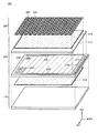
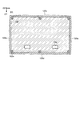
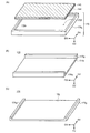
図1は、表示装置100の全体構成を示す模式的な展開図である。一例では、第1方向DX、第2方向DY、及び、第3方向DZは、互いに直交しているが、90度以外の角度で交差していてもよい。第1方向DX及び第2方向DYは、表示装置100を構成する基板の主面と平行な方向に相当し、第3方向DZは、表示装置100の厚さ方向に相当する。本実施形態においては、第1方向DX及び第2方向DYで規定されるDX−DY平面を見ることを平面視とする。また第3方向DZを含む平面、例えばDX−DZ平面又はDY−DZ平面を見ることを、断面視とする。
1. 1. Overall Configuration FIG. 1 is a schematic development view showing the overall configuration of the
表示装置100は、光源装置110、及び光源装置110と重畳する液晶表示モジュール200を有する。更に表示装置100は、液晶表示モジュール200上にタッチセンサ220を備えてもよい。
The
本実施形態においては、光源装置110から液晶表示モジュール200に向かう方向を上又は上方と定義し、液晶表示モジュール200から光源装置110に向かう方向を下又は下方と定義する。
In the present embodiment, the direction from the
液晶表示モジュール200は、第1基板202、第1基板202に対向する第2基板214、第1基板202と第2基板214を挟持する一対の偏光板216、218、及び、第1基板202と第2基板214の間に挟持される液晶層(図示しない)を有する。第1基板202は、複数の画素204、画素204を駆動するための駆動回路(走査線駆動回路208、信号線駆動回路210)、複数の端子212を有する。画素204、当該駆動回路、端子212は、導電膜、絶縁膜、半導体膜等の積層体を有する。液晶表示モジュール200は、複数の画素204を含む表示領域206、及び、表示領域206以外の領域である額縁領域を有する。
The liquid
偏光板216、218は、表示領域206と重畳して配置される。液晶表示モジュール200には、端子212を介して外部回路(図示しない)から映像信号を含む種々の信号、及び電源が供給されるこれらの信号や電源により、駆動回路が動作する。駆動回路が画素204を制御することによって、画素204上の液晶層に含まれる液晶分子の配向が制御される。光源装置110から出射された光が液晶表示モジュール200に入射し、入射した光が画素204ごとに制御され、画像が表示される。
The
タッチセンサ220は、表示領域206と重畳して配置される。タッチセンサ220のとして、例えば図1に示す相互容量方式(ミューチャル)の静電容量方式タッチセンサを用いることができる。タッチセンサ220は、第1方向DXに延在する複数の第1タッチ電極222、第1タッチ電極と交差する複数の第2タッチ電極224、及びこれらを互いに電気的に絶縁する絶縁膜(図示しない)を有する。第1タッチ電極222及び第2タッチ電極224間に静電容量が形成され、物体、例えばユーザが指などでタッチセンサ220をタッチした際に、静電容量が変化する。静電容量変化を検出することでタッチの有無を判断し、かつ、物体の位置(座標)を特定することができる。これによりユーザは種々の命令をタッチセンサ220に対して入力することができる。なお本明細書において、タッチとは物体が接触することだけでなく近接することも含む。なお、図1では光源装置110や液晶表示モジュール200、タッチセンサ220は離隔するように描かれているが、これらは互いに接着層や筐体などを用いて固定される。なお本実施形態のタッチセンサ220として、相互容量方式(ミューチャル)のタッチセンサについて説明したが、これに限定されない。タッチセンサ220として、自己容量方式(セルフ)のタッチセンサを用いてもよい。
The touch sensor 220 is arranged so as to overlap the
さらに本実施形態のタッチセンサ220は、液晶表示モジュール200とは別に設ける、いわゆるアウトセル型タッチセンサであるが、これに限定されない。タッチセンサ220は、液晶表示モジュール200と一体化されたタッチセンサ、所謂インセル型タッチパネルでもよい。インセル型タッチパネルの場合は、液晶表示モジュール200に含まれる電極や配線が、タッチ電極として機能する。
Further, the touch sensor 220 of the present embodiment is a so-called out-cell type touch sensor provided separately from the liquid
なお図1では、液晶表示モジュール200及びタッチセンサ220は、第1方向DXの長さが第2方向DYの長さより長い、所謂ランドスケールの例を示したが、これに限定されない。液晶表示モジュール200及びタッチセンサ220は、第2方向DYの長さが第1方向DXの長さが長い、所謂ポートレートであってもよい。
Note that FIG. 1 shows an example of a so-called land scale in which the length of the first direction DX is longer than the length of the second direction DY, but the liquid
2.光源装置
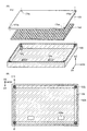
図2に光源装置110の模式的な展開図を示す。光源装置110は、リアベゼル120、及びリアベゼル120と嵌合するフロントカバー180を有する。リアベゼル120及びフロントカバー180の間に、光源基板140、光源基板140上の光学シートが配置される。光学シートには、光拡散板170、光拡散板170上のプリズムシート174、及びプリズムシート174上の偏光シート176が含まれる。光源基板140上には、複数の無機発光素子142が配置される。更に光学シートは、光拡散板170とプリズムシート174の間に波長変換膜172を有してもよい。図2では示されないが、波長変換膜172を光拡散板170とプリズムシート174の間に設けず、光源基板140と光拡散板170の間に設けてもよい。
2. Light Source Device FIG. 2 shows a schematic development view of the
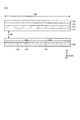
2−1.リアベゼルとフロントカバー
リアベゼル120は、光源装置110を構成する光源基板140や光学シート(光拡散板170、プリズムシート174、偏光シート176、波長変換膜172等)を収容する収納体として機能する。リアベゼル120は側板120aから120dを備え、互いに対向する一対の側板(例えば側板120aと120bの対、あるいは側板120cと120dの対)とこれらの間に位置する底板を有する。底板は側板120aから120dと一体化されている。側板120aから120dは底板の上面に対して垂直に配置することが好ましい。これにより、無機発光素子142からの光を効率よく利用して液晶表示モジュール200に供給することができる。リアベゼル120がフロントカバー180と嵌合することにより、光源基板140や、光学シート(光拡散板170、プリズムシート174、偏光シート176、波長変換膜172等)が固定される。リアベゼル120には1つ、あるいは複数の開口120eが設けられる。光源基板140と外部回路は、開口120eを介して設けられるフレキシブルプリント回路基板(FPC)等により電気的に接続される。
2-1. Rear bezel and front cover The
リアベゼル120とフロントカバー180は、アルミニウムや銅、ステンレスなどの金属を含む。リアベゼル120は、例えば厚さが1mm以上3mm以下あるいは1mm以上2mm以下の金属プレートを切削加工、プレス加工して形成することができる。フロントカバー180の厚さは、リアベゼル120の厚さと異なってもよい。フロントカバー180は、例えば0.1mm以上1mm以下あるいは0.1mm以上0.5mm以下、0.1mm以上0.4mm以下の金属板を切削加工、プレス加工して形成してもよい。
The
なお、リアベゼル120の底板は必ずしも平坦な形状を有する必要は無く、曲面形状を有していてもよい。この場合、光源基板140や光拡散板170、プリズムシート174等もこの曲面形状に合致するように配置される。
The bottom plate of the
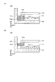
2−2.光源基板と無機発光素子
光源装置110の一部の模式的断面図を図3に示す。上述したように光源基板140はリアベゼル120内に収容される。光源基板140はリアベゼル120と接していてもよい。
2-2. Light source substrate and inorganic light emitting element FIG. 3 shows a schematic cross-sectional view of a part of the
複数の無機発光素子142は、光源基板140の上に配置され、表示領域206と重なる。無機発光素子142は、例えば格子状に配置する。隣接する無機発光素子142のピッチは、表示装置100の大きさによって任意に設定することができる。隣接する無機発光素子142間のピッチは、例えば1mm以上20mm以下、3mm以上15mm以下、あるいは5mm以上10mm以下の範囲から選択すればよい。表示領域206にわたって均一な輝度の光を供給するため、複数の無機発光素子142は均等なピッチで配置されることが好ましい。
The plurality of inorganic
無機発光素子142は、窒化ガリウム、インジウムを含む窒化ガリウムなどの無機発光体を一対の電極で挟持した発光ダイオード、及び当該発光ダイオードを保護する保護膜を有する発光素子である。無機発光素子142は、電界発光(Electroluminescence)によって発光するように構成される。無機発光体としては、例えば400nmから530nmの間に発光ピークを与える無機化合物を選択することができる。無機発光素子142では、青色の発光が保護膜を介して取り出される。あるいは保護膜中に、無機発光体からの光を変換する色変換材料を分散させた発光ダイオードを用いてもよい。当該発光ダイオードは、無機発光体からの光と、色変換材料により変換された光が混合され、白色光を発光する。色変換材料として、緑から赤色の領域の蛍光、例えば黄色の蛍光を発する蛍光材料を用いればよい。この場合には、波長変換膜172を設けず、光拡散板170とプリズムシート174が互いに接するように配置することができる。
The inorganic
各無機発光素子142の大きさに制約はなく、例えばそれぞれの占有面積が1.0×104μm2以上1.0×106μm2以下、4.0×104μm2以上5.0×105μm2以下、あるいは9.0×104μm2以上2.5×105μm2以下の発光ダイオードを用いることができる。一例として大きさが320μm×300μm程度の所謂マイクロLEDを無機発光素子142として用いることができる。
There is no limitation on the size of each inorganic
光源装置110はさらに、無機発光素子142を覆うようにオーバーコート144を有してもよい。オーバーコート144は光源基板140と接してもよい。オーバーコート144は無機発光素子142を保護し、光源基板140から分離することを防ぐ機能を有するとともに、無機発光素子142に起因する凹凸を吸収して平坦な表面を与える。また、無機発光素子142は比較的指向性の高い光を与えるが、オーバーコート144により無機発光素子142からの光を広げる、あるいは拡散させることができる。
The
オーバーコート144は可視光領域の透過率が高いことが好ましい。オーバーコート144は、例えばアクリル系樹脂やポリカーボネート、あるいはポリエチレンテレフタレートなどのポリエステルに例示される高分子材料、あるいは酸化ケイ素などのケイ素含有無機化合物などを含む。オーバーコート144の厚さは、無機発光素子142を覆う程度の厚さが好ましい。オーバーコート144の厚さは、例えば200μm以上1mm以下、400μm以上1mm以下、あるいは500μm以上800μm以下の範囲から選択すればよい。
The
2−3.光拡散板
光拡散板170は、無機発光素子142からの光を拡散し、均一な発光面を与える。光拡散板170の厚さは、例えば0.5mm以上2mm以下、あるいは0.75mm以上1.5mm以下の範囲から選択することができる。光拡散板170を配置することで指向性の高い無機発光素子142からの光が効果的に拡散され、光拡散板170が配置される面内における輝度の分布が低下する。その結果、プリズムシート174や波長変換膜172に対して均一な輝度で光を提供することができる。
2-3. Light diffusing plate The
光拡散板170は、無機発光素子142から離隔して配置される。具体的には、光源基板140の上面(DX−DZ平面のうち液晶表示モジュール200により近い面)から光拡散板170の底面(DX−DZ平面のうち液晶表示モジュール200により遠い面)までの距離(光学距離とも呼ばれる)は、1mm以上3mm以下、あるいは1.5mm以上2.5mm以下とする。従って、光拡散板170と無機発光素子142、あるいは光拡散板170とオーバーコート144は、直接接しない。光拡散板170と無機発光素子142を離隔させるための構造については後述する。
The
2−4.波長変換膜
波長変換膜172は、無機発光素子142から出射し、光拡散板170で拡散された光の波長を変換して白色光を生成する機能を有する膜であり、高分子材料中に蛍光体が分散した構造を有する。蛍光体は、無機発光素子142から射出される青色の光を吸収し、緑から赤色の領域の蛍光、例えば黄色の蛍光を発する蛍光物質を含む。蛍光物質としては、上述した色変換材料を用いればよい。あるいは、蛍光体に替わり、粒径が数nmから数十nmの量子ドットを用いてもよい。
2-4. Wavelength conversion film The
波長変換膜172は、別途作製した1つの独立膜として光拡散板170の上、あるいは下に配置してもよく、あるいは上述した及び蛍光体または量子ドットを含む分散液を光拡散板170の上または下に塗布し、その後硬化することで形成してもよい。
The
2−5.プリズムシート
プリズムシート174は、光拡散板170や波長変換膜172を通過した後の光を上方向へ効率よく出射させるための光学フィルムであり、表面に複数のプリズム形状が平行に配置された構造を有する。
2-5. Prism sheet The
2−6.偏光シート
偏光シート176は、例えば異方性反射偏光子である。より具体的には、偏光シート176は、円偏光又は楕円偏光で偏光シートの透過軸と一致しない光を、偏光シート176内に形成されている多層膜により反射させ、反射成分を繰り返し回収する。光を効率よく反射することで光の損失を防ぎ、出射光の輝度向上が図れる。また、偏光シート176を設けることで、無機発光素子から出射する指向性の高い光を拡散するという効果を奏する。
2-6. Polarizing sheet The
2−7.スペーサ
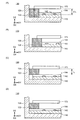
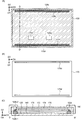
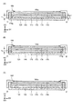
図4(A)にそれぞれリアベゼル120、光源基板140、及び光拡散板170を含む模式的展開図と上面図を、図4(B)にリアベゼル120と無機発光素子142の上面図示す。図4(B)では光源基板140と光拡散板170は図示されていない。上述したように光源装置110では、光拡散板170は無機発光素子142から離隔するように配置され、このための構造としてスペーサ122がリアベゼル120内に配置される。なお他の光学シート、例えば波長変換膜が無機発光素子142に一番近傍に配置される場合は、下記の説明は光拡散板170を波長変換膜172に置き換えて読めばよい。
2-7. Spacer FIG. 4 (A) shows a schematic development view and a top view including a
(1)スペーサと無機発光素子との位置関係
スペーサ122は光拡散板170の下に設けられ、スペーサ122の少なくとも一部が平面視で光拡散板170と重なる。スペーサ122は光源基板140の下では無機発光素子142と重なってもよいが、光源基板140の上では無機発光素子142と重ならないように配置されることが好ましい。より具体的には、図4(B)に示すように、光源基板140の上面のうち複数の無機発光素子142と重なる領域を領域142aと定義すると、領域142aがスペーサ122と重畳しないよう、スペーサ122と光源基板140はリアベゼル120内に配置される。換言すると、スペーサ122は、光源基板140上面のうち無機発光素子142が設けられない領域に配置される。このようにスペーサ122を配置することで、無機発光素子142からの光がスペーサ122によって遮られることなく、光拡散板170へ入射する。
(1) Positional Relationship between Spacer and Inorganic Light Emitting Element The
(2)スペーサの形状と配置
スペーサ122の形状や配置の例を図4(A)乃至図10(B)を用いて説明する。図5(A)乃至図5(C)は図4(B)の鎖線A−A´に沿った断面の模式図である。図5(A)乃至図5(C)では見やすさを考慮し、無機発光素子142やオーバーコート144は図示しない。図6(A)乃至図6(C)、図9(A)乃至図9(C)は図5(A)における領域130の拡大図である。図7(A)乃至図8はリアベゼル120とスペーサ122の上面模式図である。
(2) Shape and Arrangement of Spacer An example of the shape and arrangement of the
例えば図4(A)乃至図5(A)に示すように、スペーサ122は光源基板140の上面と平行な面において閉じた形状を有し、平面視で複数の無機発光素子142を囲むように配置する。一例として液晶表示モジュール200の第1基板202が四角形の場合、リアベゼル120やこれに収容される光源基板140なども四角形の形状を有するため、スペーサ122は複数の直線部を有し、当該直線部がリアベゼル120の側板120aから120dに沿うように配置される。
For example, as shown in FIGS. 4A to 5A, the
スペーサ122はリアベゼル120の側板120aから120dのすべて、あるいは一部と接するように配置することができる(図5(A))。スペーサ122はさらに、リアベゼル120の底板の上面と接するように配置してもよい(図5(A))。この場合、スペーサ122と光源基板140は重ならず、光源基板140はスペーサ122によって囲まれる。光源基板140は、図示しない接着剤や両面テープなどを利用してリアベゼル120の底板の上面に固定される。
The
図5(A)では、スペーサ122は光拡散板170の底面と接するが、上述したように、光拡散板170と光源基板140の間に波長変換膜172を配置することも可能である。この場合には、スペーサ122は波長変換膜172の底面と接するように配置される(図5(B))。波長変換膜172を設けない場合には、プリズムシート174の底面が光拡散板170と接するように配置される(図5(C))。
In FIG. 5A, the
図6(A)は領域130の拡大図である。図6(A)に示すように、光源基板140がスペーサ122と重ならない場合には、スペーサ122の厚さは光源基板140の厚さよりも厚いほうが好ましい。例えばスペーサ122の厚さt1と光源基板140の厚さとの差Δt1は、1mm以上3mm以下、あるいは1.5mm以上2.5mm以下の範囲である。光学シート(図6(A)では光拡散板170)の底面と光源基板140の上面の間隔は、差Δt1に等しい距離で保持される。
FIG. 6A is an enlarged view of the
スペーサ122は必ずしもリアベゼル120の側板120a乃至120dの全てと接する必要は無く、一部、あるいは全ての側板から離隔してもよい。スペーサ122をリアベゼル120の全ての側板120a乃至120dから離隔した例を、図6(B)に示す。あるいはスペーサ122は、光源基板140、あるいはその上に設けられるオーバーコート144と接するよう、光源基板140と重なるように設けてもよい(図6(C))。図6(C)の構成に加えて、光源基板140はリアベゼル120の側板120aから120dの全て、あるいは一部と接してもよい(図6(D))。オーバーコート144を設ける場合、オーバーコート144の厚さとスペーサ122の厚さt1の和は1mm以上3mm以下、あるいは1.5mm以上2.5mm以下とする。オーバーコート144を設けない場合には、スペーサ122の厚さt1は1mm以上3mm以下、あるいは1.5mm以上2.5mm以下とする。スペーサ122の厚さt1が、光拡散板170の底面と光源基板140の上面間の距離となる。
The
あるいは図7(A)に示すように、スペーサ122として互いに分離し、対向する一対の直線状ロッド122a及び122b(第1の直線状ロッド122a及び122b)を設けてもよい。一対の直線状ロッド122a及び122bはそれぞれ、互いに対向する2つの側板(ここでは側板120cと120d)に沿って延伸する。このような配置であっても一対の直線状ロッド122a及び122bによって安定的に光拡散板170を保持し、光源基板140と光拡散板170間の距離を維持することができる。また図7(B)に示すように、スペーサ122は互いに対向するさらに別の一対の直線状ロッド122c及び122d(第2の直線状ロッド122c及び122d)を有してもよい。一対の直線状ロッド122c及び122dは、他の一対の側板(ここでは側板120aと120b)にそれぞれ沿って延伸する。直線状ロッド122c及び122dの延伸する方向と、一対の直線状ロッド122a及び122bの延伸する方向が、直交するように配置することができる。
Alternatively, as shown in FIG. 7A, a pair of
あるいは図8に示すように、スペーサ122として、互いに分離した複数のパッド122eを設けてもよい。少なくとも3つのパッド122eをリアベゼル120内に配置することで、光拡散板170を保持することができる。これにより光源基板140と光学シート間の距離を維持することができる。より安定的に光拡散板170を保持するため、4つ以上のパッド122eを設けてもよい。この場合、4つのパッド122eが光拡散板170の底板の角部に位置することが好ましい。5つ以上のパッド122eを設ける場合は、そのうちの3つのパッド122eが並ぶ方向が、リアベゼル120の側板(図8では側板120c及び120d)が延伸する方向と平行、あるいは実質的に平行となるように複数のパッド122eを配列させることが好ましい。
Alternatively, as shown in FIG. 8, a plurality of
(3)断面形状
DY−DZ平面におけるスペーサ122の断面形状は、四角形などの多角形に限られず、例えば図9(A)に示すように円でもよく、楕円でもよい。
(3) Cross-sectional shape The cross-sectional shape of the
あるいは図9(B)に示すように、スペーサ122は断面視で階段形状を有していてもよい。図9(B)に示すスペーサ122には1つ、あるいは複数のステップ122fが形成される。ステップ122fとは、底面と最上面の間に位置する面であり、光源基板140の上面に平行な面(DX−DY平面)である。光拡散板170は、ステップ122f上に、ステップ122fと接するように配置される。ステップ122fを有するスペーサ122は、リアベゼル120の底板の上面と接するように配置する。ステップ122fの高さt2(すなわち、スペーサ122の底面からステップ122fまでの距離)と光源基板140の厚さの差Δt2は、1mm以上3mm以下、あるいは1.5mm以上2.5mm以下の範囲とする。またステップ122fを有するスペーサ122は、光源基板140と重なるように配置してもよい(図9(C))。(図9(C)に示す構成では、ステップ122fの高さt2、更にオーバーコート144を設ける場合には高さt2とオーバーコート144の厚さの和、は、上述したΔt2の範囲と同等である。図示しないが、波長変換膜172が光源基板140と光拡散板170の間に配置される場合には、ステップ122fと波長変換膜172が互いに接するように、波長変換膜172がスペーサ122上に配置される。
Alternatively, as shown in FIG. 9B, the
あるいは、スペーサ122は複数の層で構成されていてもよい。例えば図10(A)及び図10(B)それぞれに示すように、スペーサ122は第1の支持層122g、及び第1の支持層122g上に位置し、第1の支持層122gと接する第2の支持層122hを備えてもよい。第1の支持層122gと第2の支持層122hは互いに異なる材料を含んでもよい。第1の支持層122gは第1の材料として例えば金属を含み、第2の支持層122hは第2の材料として例えば高分子材料を含んでもよい。第2の支持層122hは少なくとも一方の面が接着性を有するように構成してもよい。スペーサ122が複数の支持層で構成される場合、スペーサ122の厚さとは、当該複数の支持層の厚さの和である。
Alternatively, the
(4)材料
スペーサ122を構成する材料に制約はなく、例えばアルミニウムや銅、亜鉛、鉄、ステンレス、真鍮などの金属や合金でもよく、あるいは高分子材料でも良い。高分子材料としては、アクリル樹脂、エポキシ樹脂、ウレタン樹脂、シリコーン樹脂、フェノール樹脂、ポリエチレンやポリプロピレンなどのポリオレフィン、ポリスチレン、ポリアクリロニトリル、ポリブタジエン、ポリイソプレン、ポリエチレンなどのポリエステル、ポリカルボナートなどが挙げられる。
(4) Material The material constituting the
上述したように光源装置110では、複数の無機発光素子142が配置される光源基板140及び光学シート(光拡散板170、プリズムシート174、偏光シート176等)がリアベゼル120とフロントカバー180の間に収容され、互いに固定される。光源装置110の上に液晶表示モジュール200が配置され、表示装置100を構成する。光源装置110内ではスペーサ122が光拡散板170の下に配置され、光源基板140と光学シートとの間に一定の間隔が保持される。従って、無機発光素子142から指向性の高い光が出射されても、光源基板140と光拡散板170の間の空間で出射光が拡散する。また、出射光がこの空間内で反射を繰り返すことで指向性がさらに低下する。その結果、光拡散板170の底面において輝度の高い領域(ホットスポット)の局所的な発生が抑制される。更に、光源基板140と光拡散板170の間の空間によって強度分布が低下した光が光拡散板170によりさらに拡散し、均一な輝度で液晶表示モジュール200へ光が入射される。このため、表示領域206に対して均一な輝度の光が提供され、表示装置100は高品質な表示が可能となる。
As described above, in the
さらに本実施形態の表示装置100では、光源として機能する無機発光素子142は、平面視で表示領域206と重畳して配置することができる。光源を額縁領域に配置する構成と比較すると、光を液晶表示モジュール200側へ反射させるための反射板が不要となる。よって光源装置を構成する部品数を低減することができる。このことは表示装置の薄型化に寄与する。さらに、額縁領域に光源を配置する必要がないため、額縁領域を小さくし、表示装置100全体に対する表示領域206の面積を大きくすることが可能となる。このため、本実施形態を適用することで、デザイン性に優れた表示装置を提供することが可能となる。
Further, in the
<第2実施形態>
本実施形態では、第1実施形態の光源装置110と異なる構造を有する光源装置112について説明する。第1実施形態で述べた構造と同一、あるいは類似する構造については説明を割愛することがある。
<Second Embodiment>
In this embodiment, the
第2実施形態の光源装置112は、光学シート(光拡散板170又は波長変換膜172)に凹部、貫通孔、切り欠き、又は溝が設けられ、スペーサ122の少なくとも一部が当該凹部、貫通孔、切り欠き、又は溝内に位置する点で、第1実施形態の光源装置110と異なる。具体的な構造を図11(A)乃至図15(B)を用いて以下に説明する。
In the
図11(A)は光源装置112に含まれるリアベゼル120、スペーサ122、光源基板140、光学シートのうち光拡散板170を展開した模式図であり、図11(B)はリアベゼル120とスペーサ122の上面模式図である。図11(A)に示すように光源装置112は、リアベゼル120内に配置されるスペーサ122として支持ピン122jを有する。支持ピン122jの数に制約はないが、少なくとも3つ以上であればよく、4つ以上が好ましい。4つの支持ピン122jを配置する場合、支持ピン122jはリアベゼル120の4つのコーナーに設置することが好ましい。4つ以上の支持ピン122jを配置する場合、パッド122eと同様、そのうちの3つが並ぶ方向がリアベゼル120の側板が延伸する方向と平行、あるいは実質的に平行となるように支持ピン122jを配列させることが好ましい。なお他の光学シート、例えば波長変換膜が無機発光素子142に一番近傍に配置される場合は、本実施形態の光拡散板170を波長変換膜172に置き換えて読めばよい。
FIG. 11A is a schematic view of the
支持ピン122jは、領域142aと重ならないように配置される。換言すると、平面視で、光源基板140の上面のうち複数の無機発光素子142と重なる領域142a(図4(B)参照)が支持ピン122jと重畳しない(図11(B))。
The
一方、光拡散板170には支持ピン122jの位置に対応するように複数の貫通孔170aが設けられる(図11(A))。各支持ピン122jの少なくとも一部が対応する貫通孔170a内に配置する。例えば図12(A)に示すように、各支持ピン122jは下部122j−1と上部122j−2を有し、上部122j−2が貫通孔170aを貫通し、下部122j−1が貫通孔170aを貫通しない。従って、上部122j−2の断面(光源基板140の上面に平行な断面)の面積は、下部122j−1の面積よりも小さい。
On the other hand, the
図12(B)に図11(B)の鎖線B−B´に沿った模式的断面図を示す。図12(B)に示すように、上部122j−2は貫通孔170aを貫通してもよい。また図示しないが、上部122j−2が貫通孔170aを完全に貫通しなくてもよい。
FIG. 12B shows a schematic cross-sectional view taken along the chain line BB'of FIG. 11B. As shown in FIG. 12B, the
このような構成では、下部122j−1の厚さ(第3方向DZの長さ)t3が光源基板140と光拡散板170との離隔に寄与する。具体的には、支持ピン122jが光源基板140と重ならない場合には、下部122j−1の厚さt3と光源基板140の厚さの差Δt3は、1mm以上3mm以下、あるいは1.5mm以上2.5mm以下の範囲とする。厚さΔt3が光源基板140と光拡散板170との距離となる。一方、支持ピン122jが光源基板140上に配置される場合には、下部122j−1の厚さt3、更にオーバーコート144上に支持ピンを配置する場合には厚さt3とオーバーコート144の厚さの和、が上述した範囲と同等である。
In such a configuration, the thickness t 3 of the
あるいは図12(C)に示すように、光拡散板170には貫通孔170aに替わって凹部170bを形成し、凹部170b内に支持ピン122jの一部を収納してもよい。図12(C)に示す構成では、支持ピン122jが光源基板140と平面視で重ならない場合には、支持ピン122jの凹部170bから露出した部分の長さLと光源基板140の厚さの差が、光源基板140と光拡散板170間の距離となる。一方、支持ピン122jが光源基板140上に配置される場合には、長さL、更にオーバーコート144を配置する場合には長さLとオーバーコート144の厚さの和、が、上述した範囲とする。
Alternatively, as shown in FIG. 12C, a
あるいは図13(A)に示すように、貫通孔170aや凹部170bに替わって、光拡散板170の角部に切り欠き170cを光拡散板170に形成してもよい。切り欠き170cと支持ピン122jの一部は重畳して配置する。図13(A)の鎖線C−C´に沿った断面の模式図(図13(B))に示すように、支持ピン122jの上部122j−2が切り欠き170cと重なり、下部122j−1の上面が光拡散板170の底面と接する。
Alternatively, as shown in FIG. 13A, a
あるいは図14(A)に示すように、スペーサ122として一対のレール122kを設けてもよい。一対のレール122kは互いに対向する側板(図14(A)に示した例では側板120c及び120d)に沿うよう、これらの側板と平行に延伸させる。また一対のレール122kは平面視で領域142aを挟持するように配置される。一方、光拡散板170には、一対のレール122kと対応する位置に一対の溝170dが設けられる(図14(B))。各レール122kは、少なくとも一部が溝170dに収容される。例えば図14(A)の鎖線D−D´に沿った断面の模式図(14(C))に示すように、各レール122kは、側板と平行に延伸し、溝170dの幅よりも小さい幅を有する上部122k−2、及び側板と平行に延伸し、溝170dの幅よりも大きい下部122k−1を有する。光拡散板170の底面は下部122k−1の上面と接する。溝170dは光拡散板170を貫通していてもよく、図示しないが光拡散板170を貫通しない有底溝でもよい。
Alternatively, as shown in FIG. 14A, a pair of
あるいは図15(A)に示すように、スペーサ122として一対のレール122kを設ける場合、溝170dに替わって、光拡散板170の長辺又は短辺に沿った、即ち第1方向DX又は第2方向DYに沿った直線状の一対の切り欠き170eを形成してもよい。図15(A)の鎖線E−E´に沿った断面の模式図(図15(B))に示すように、一対の切り欠き170eに挟まれる領域の長さWは、一対のレール122kの上部122k−2間の距離よりも短く、下部122k−1間の距離よりも長い。これにより、一対のレール122kによって光源基板140と光拡散板170間の空間が保持される。
Alternatively, as shown in FIG. 15A, when a pair of
図示しないが、スペーサ122として二対のレール122kを設けてもよい。この場合、一対のレール122kが延伸する方向が他の一対のレール122kが延伸する方向と垂直になるようにレール122kを配置することが好ましい。具体的には、スペーサ122として、第1方向DXに延伸する一対のレール122k並びに第2方向DYに沿った一対のレール122kを設ければよい。光拡散板170には、二対のレール122kに対応する二対の溝170d、あるいは二対の切り欠き170eが形成される。
Although not shown, two pairs of
なお、波長変換膜172が光源基板140と光拡散板170の間に設けられる場合、貫通孔170a、凹部170b、切り欠き170c、溝170dは波長変換膜172に形成すればよい。
When the
本実施形態の光源装置112においても、支持ピン122jやレール122kを含むスペーサ122によって、無機発光素子142と光学シートを互いに離隔することができ、また、無機発光素子142と光学シートの間の距離を一定に保つことができる。このため、第1実施形態と同様の効果を奏する。
Also in the
<第3実施形態>
本実施形態では、光源装置110や112と異なる構造を有する光源装置114について、図16(A)から図18(C)を用いて説明する。第1及び第2実施形態で述べた構造と同一、あるいは類似する構造については説明を割愛することがある。
<Third Embodiment>
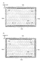
In the present embodiment, the light source device 114 having a structure different from that of the
光源装置114では、光学シートが第1及び第2実施形態で述べたスペーサ122としても同時に機能する点で、第1実施形態の光源装置110及び第2実施形態の光源装置112と相違する。具体的な構成を図16(A)に示す。図16(A)では見やすさを考慮し、光源基板140が光拡散板170の上に位置するように描かれている。従って図16(A)では、無機発光素子142やオーバーコート144は光源基板140の下に位置する。図16(A)に示すように、光源装置114の光拡散板170は、凹部170fを有する。凹部170fは、光源基板140の上面のうち複数の無機発光素子142と重なる領域である、領域142aの全体と重なる。換言すると、光拡散板170は、光源基板140の上面と平行な面において閉じた形状を有する側板170gを有する。側板170gに囲まれた領域170hが凹部170fの底板として機能し、領域142aの全体と重なる。底板は側板170gと一体化されている。
The light source device 114 differs from the
図17(A)に光源装置114が有するリアベゼル120、光源基板140、及び光拡散板170が展開された状態を、図17(B)にこれらの模式的上面図を、図17(B)の鎖線D−D´に沿った断面の模式図を図18(A)に示す。図17(A)、図17(B)及び図18(A)に示すように、光拡散板170の凹部170fの開口側がリアベゼル120側に位置する。光源基板140、及びその上に設けられる無機発光素子142は、リアベゼル120と光拡散板170の間に位置し、凹部170fが領域142aを覆う。図18(A)に示すように、光拡散板170の側板170gはリアベゼル120と接し、凹部170fの底板は光源基板140から離隔する。従って側板170gが光源装置110や112のスペーサ122としても機能する。
FIG. 17 (A) shows a state in which the
側板170gの高さh1(すなわち、側板170gの厚さと底板の厚さの差)と光源基板140の厚さの差h2が、光源基板140と光学シート間の距離GPに相当する。差h2は1mm以上3mm以下、又は1.5mm以上2.5mm以下、光拡散板170の底板の厚さが0.5mm以上2mm以下、又は0.75mm以上1.5mm以下が好ましい。
The height h 1 of the
あるいは図18(B)に示すように、側板170gは光源基板140と平面視で重なるように配置してもよい。この場合、側板170gと光源基板140、あるいは側板170gとオーバーコート144が互いに接し、底板は領域142aの全体を覆う。側板170gの高さh1、更にオーバーコート144を設ける場合にはオーバーコート144の厚さと側板170gの高さh1の和、は、1mm以上3mm以下、あるいは1.5mm以上2.5mm以下とする。なお、波長変換膜172を光源基板140と光拡散板170の間に配置する場合、光拡散板170に凹部170fを設けず、波長変換膜172に凹部を形成すればよい(図18(C))。この場合も、波長変換膜172の凹部は、領域142aの全体を覆う。
Alternatively, as shown in FIG. 18B, the
光拡散板170の側板170gは、光源基板140の上面と平行な面において閉じた形状を必ずしも有する必要は無い。例えば図16(B)に示すように、光拡散板170の端部のうち互いに対向する端部は、光源基板140の方向へ屈曲してもよい。光拡散板170は、互いに分離した一対の側板170g、及び、側板170gの間に位置する平坦部170jを有してもよい。一対の側板170gは、光拡散板170の長辺に沿って、即ち第1方向DXに沿って配置されていてもよく(図16(B))、短辺に沿って、即ち第2方向DYに沿って配置されていてもよい(図16(C))。図16(B)及び(C)に示す場合でも、平坦部170jが領域142aの全体を覆う。図示しないが、光源基板140と光拡散板170の間に波長変換膜172を配置し、波長変換膜172が上述した光拡散板170と同様の構造を有していてもよい。
The
本実施形態に示した光源装置114では、側板170gが光源基板140と光学シートの間隔を保持するスペーサ122として機能する。従って、光拡散板170のうち光拡散を主に担う部分(例えば底板や平坦部170j)と光源基板140を互いに離隔することができる。このため、第1実施形態と同様の効果を奏する。
In the light source device 114 shown in the present embodiment, the
なお本実施形態では、光拡散板又は波長変換膜を屈曲させる例について述べたが、これに限定されない。光拡散板又は波長変換膜に代えて、光学シートのうち無機発光素子142に一番近傍のものを屈曲させてもよい。
In this embodiment, an example of bending the light diffusing plate or the wavelength conversion film has been described, but the present invention is not limited to this. Instead of the light diffusing plate or the wavelength conversion film, the optical sheet closest to the inorganic
本発明の実施形態として上述した各実施形態は、相互に矛盾しない限りにおいて、適宜組み合わせて実施することができる。また、各実施形態の表示装置を基にして、当業者が適宜構成要素の追加、削除もしくは設計変更を行ったもの、または、工程の追加、省略もしくは条件変更を行ったものも、本発明の要旨を備えている限り、本発明の範囲に含まれる。 Each of the above-described embodiments of the present invention can be appropriately combined and implemented as long as they do not contradict each other. Further, based on the display device of each embodiment, those skilled in the art have appropriately added, deleted or changed the design of components, or added, omitted or changed the conditions of the process of the present invention. As long as it has a gist, it is included in the scope of the present invention.
上述した各実施形態の態様によりもたらされる作用効果とは異なる他の作用効果であっても、本明細書の記載から明らかなもの、または、当業者において容易に予測し得るものについては、当然に本発明によりもたらされるものと解される。 Of course, other effects different from those brought about by the embodiments of the above-described embodiments that are clear from the description of the present specification or that can be easily predicted by those skilled in the art will naturally occur. It is understood that it is brought about by the present invention.
本明細書にて開示した構成から得られる表示装置の一例を以下に付記する。 An example of a display device obtained from the configuration disclosed in the present specification is added below.
(1)収納体と、
前記収納体上に位置し、前記収納体内に収容される光源基板と、
前記光源基板上の複数の無機発光素子と、
前記複数の無機発光素子上に位置し、前記収納体内に収容され、前記光源基板から離隔する光学シートと、及び
前記収納体内に収容され、前記光学シートの底面と接するスペーサと、
を備え、
前記光源基板の上面のうち前記複数の無機発光素子と重なる領域は、前記スペーサと重畳しない、光源装置。
(1) Storage body and
A light source substrate located on the storage body and housed in the storage body,
With the plurality of inorganic light emitting elements on the light source substrate,
An optical sheet located on the plurality of inorganic light emitting elements, housed in the storage body and separated from the light source substrate, and a spacer housed in the storage body and in contact with the bottom surface of the optical sheet.
With
A light source device in which a region of the upper surface of the light source substrate that overlaps with the plurality of inorganic light emitting elements does not overlap with the spacer.
(2)前記スペーサは前記光源基板を囲む、(1)に記載の光源装置。 (2) The light source device according to (1), wherein the spacer surrounds the light source substrate.
(3)前記スペーサは前記複数の無機発光素子を囲む、(1)に記載の光源装置。 (3) The light source device according to (1), wherein the spacer surrounds the plurality of inorganic light emitting elements.
(4)前記スペーサは前記光源基板と平面視で重なる、(1)に記載の光源装置。 (4) The light source device according to (1), wherein the spacer overlaps the light source substrate in a plan view.
(5)前記複数の無機発光素子を覆い、前記光源基板と接するオーバーコートをさらに有し、
前記スペーサは前記オーバーコートと接する、(1)に記載の光源装置。
(5) Further having an overcoat that covers the plurality of inorganic light emitting elements and is in contact with the light source substrate.
The light source device according to (1), wherein the spacer is in contact with the overcoat.
(6)前記スペーサは前記収納体の側板と接する、(1)に記載の光源装置。 (6) The light source device according to (1), wherein the spacer is in contact with a side plate of the housing.
(7)前記収納体は、互いに対向する第1の側板及び第2の側板を有し、
一対の前記スペーサは、前記第1の側板及び第2の側板それぞれに沿って延伸する、(1)に記載の光源装置。
(7) The storage body has a first side plate and a second side plate facing each other.
The light source device according to (1), wherein the pair of spacers extends along the first side plate and the second side plate, respectively.
(8)前記収納体は、互いに対向する第3の側板と第4の側板を有し、
別の一対の前記スペーサは、前記第3の側板及び第4の側板それぞれに沿って延伸し、
前記一対のスペーサが延伸する方向と前記別の一対のスペーサが延伸する方向が直交する、(7)に記載の光源装置。
(8) The storage body has a third side plate and a fourth side plate facing each other.
Another pair of the spacers extends along the third side plate and the fourth side plate, respectively.
The light source device according to (7), wherein the direction in which the pair of spacers is stretched is orthogonal to the direction in which the other pair of spacers is stretched.
(9)少なくとも3つの前記スペーサを有する、(1)に記載の光源装置。 (9) The light source device according to (1), which has at least three of the spacers.
(10)前記スペーサは、前記光学シートと接するステップを有する、(1)に記載の光源装置。 (10) The light source device according to (1), wherein the spacer has a step in contact with the optical sheet.
(11)前記スペーサは、
第1の支持層と、及び
前記第1の支持層上に位置し、前記第1の支持層と接する第2の支持層と、
を有し、
前記第1の支持層及び前記第2の支持層はそれぞれ、互いに異なる第1の材料及び第2の材料を含む、(1)に記載の光源装置。
(11) The spacer is
A first support layer and a second support layer located on the first support layer and in contact with the first support layer.
Have,
The light source device according to (1), wherein the first support layer and the second support layer contain different first materials and second materials, respectively.
(12)前記スペーサは下部及び上部を有し、
前記光学シートは複数の凹部又は複数の貫通孔を備え、
前記スペーサの上部は、複数の貫通孔のそれぞれの前記凹部又は前記貫通孔内に位置する、(1)に記載の光源装置。
(12) The spacer has a lower part and an upper part.
The optical sheet has a plurality of recesses or a plurality of through holes.
The light source device according to (1), wherein the upper portion of the spacer is located in the recess or the through hole of each of the plurality of through holes.
(13)前記収納体は、互いに対向する第1の側板及び第2の側板を有し、
一対の前記スペーサは、前記第1の側板及び第2の側板にそれぞれに沿って延伸し、
前記光学シートは一対の溝を有し、
前記一対のスペーサはそれぞれ、対応する前記溝内に少なくとも一部が位置する、(1)に記載の光源装置。
(13) The storage body has a first side plate and a second side plate facing each other.
The pair of spacers extends along the first side plate and the second side plate, respectively.
The optical sheet has a pair of grooves and
The light source device according to (1), wherein at least a part of each of the pair of spacers is located in the corresponding groove.
(14)収納体と、
前記収納体上に位置し、前記収納体内に収容される光源基板と、
前記光源基板上の複数の無機発光素子と、及び
前記複数の無機発光素子上に位置し、前記収納体内に収容される光学シートと、
を備え、
前記光学シートは、前記複数の無機発光素子と重なる平坦部、及び前記平坦部を挟む一対の側板を有し、
前記一対の側板は前記光源基板の方向へ屈曲している、光源装置。
(14) Storage body and
A light source substrate located on the storage body and housed in the storage body,
A plurality of inorganic light emitting elements on the light source substrate, and an optical sheet located on the plurality of inorganic light emitting elements and housed in the storage body.
With
The optical sheet has a flat portion that overlaps with the plurality of inorganic light emitting elements, and a pair of side plates that sandwich the flat portion.
A light source device in which the pair of side plates are bent toward the light source substrate.
(15)前記一対の側板は前記収納体と接する、(14)に記載の光源装置。 (15) The light source device according to (14), wherein the pair of side plates are in contact with the storage body.
(16)前記一対の側板は前記光源基板と重なる、(14)に記載の光源装置。 (16) The light source device according to (14), wherein the pair of side plates overlaps with the light source substrate.
(17)収納体と、
前記収納体上に位置し、前記収納体内に収容される光源基板と、
前記光源基板上の複数の無機発光素子と、及び
前記複数の無機発光素子上に位置し、前記収納体内に収容される光学シートと
を備え、
前記光学シートは、前記複数の無機発光素子と重なる凹部と、前記凹部を囲む側板を有する、光源装置。
(17) Storage body and
A light source substrate located on the storage body and housed in the storage body,
A plurality of inorganic light emitting elements on the light source substrate and an optical sheet located on the plurality of inorganic light emitting elements and housed in the storage body are provided.
The optical sheet is a light source device having a recess that overlaps the plurality of inorganic light emitting elements and a side plate that surrounds the recess.
(18)前記側板は前記収納体と接する、(17)に記載の光源装置。 (18) The light source device according to (17), wherein the side plate is in contact with the storage body.
(19)前記光源基板は前記光学シートの前記凹部に収容される、(17)に記載の光源装置。 (19) The light source device according to (17), wherein the light source substrate is housed in the recess of the optical sheet.
(A1)光源装置と、及び前記光源装置上の液晶表示モジュールとを備え
前記光源装置は、
収納体と、
前記収納体上に位置し、前記収納体内に収容される光源基板と、
前記光源基板上の複数の無機発光素子と、
前記複数の無機発光素子上に位置し、前記収納体内に収容され、前記光源基板から離隔する光学シートと、及び
前記収納体内に収容され、前記光学シートの底面と接するスペーサと、
を備え、
前記光源基板の上面のうち前記複数の無機発光素子と重なる領域は、前記スペーサと重畳しない、表示装置。
(A1) The light source device includes a light source device and a liquid crystal display module on the light source device.
With the storage body
A light source substrate located on the storage body and housed in the storage body,
With the plurality of inorganic light emitting elements on the light source substrate,
An optical sheet located on the plurality of inorganic light emitting elements, housed in the storage body and separated from the light source substrate, and a spacer housed in the storage body and in contact with the bottom surface of the optical sheet.
With
A display device in which a region of the upper surface of the light source substrate that overlaps with the plurality of inorganic light emitting elements does not overlap with the spacer.
(A2)前記スペーサは前記光源基板を囲む、(A1)に記載の表示装置。 (A2) The display device according to (A1), wherein the spacer surrounds the light source substrate.
(A3)前記スペーサは前記複数の無機発光素子を囲む、(A1)に記載の表示装置。 (A3) The display device according to (A1), wherein the spacer surrounds the plurality of inorganic light emitting elements.
(A4)前記スペーサは前記光源基板と平面視で重なる、(A1)に記載の表示装置。 (A4) The display device according to (A1), wherein the spacer overlaps the light source substrate in a plan view.
(A5)前記複数の無機発光素子を覆い、前記光源基板と接するオーバーコートをさらに有し、
前記スペーサは前記オーバーコートと接する、(A1)に記載の表示装置。
(A5) Further having an overcoat that covers the plurality of inorganic light emitting elements and is in contact with the light source substrate.
The display device according to (A1), wherein the spacer is in contact with the overcoat.
(A6)前記スペーサは前記収納体の側板と接する、(A1)に記載の表示装置。 (A6) The display device according to (A1), wherein the spacer is in contact with a side plate of the storage body.
(A7)前記収納体は、互いに対向する第1の側板及び第2の側板を有し、
一対の前記スペーサは、前記第1の側板及び第2の側板それぞれに沿って延伸する、(A1)に記載の表示装置。
(A7) The storage body has a first side plate and a second side plate facing each other.
The display device according to (A1), wherein the pair of spacers extends along each of the first side plate and the second side plate.
(A8)前記収納体は、互いに対向する第3の側板と第4の側板を有し、
別の一対の前記スペーサは、前記第3の側板及び第4の側板それぞれに沿って延伸し、
前記一対のスペーサが延伸する方向と前記別の一対のスペーサが延伸する方向が直交する、(A7)に記載の表示装置。
(A8) The storage body has a third side plate and a fourth side plate facing each other.
Another pair of the spacers extends along the third side plate and the fourth side plate, respectively.
The display device according to (A7), wherein the direction in which the pair of spacers is stretched is orthogonal to the direction in which the other pair of spacers is stretched.
(A9)少なくとも3つの前記スペーサを有する、(A1)に記載の表示装置。 (A9) The display device according to (A1), which has at least three of the spacers.
(A10)前記スペーサは、前記光学シートと接するステップを有する、(A1)に記載の表示装置。 (A10) The display device according to (A1), wherein the spacer has a step in contact with the optical sheet.
(A11)前記スペーサは、
第1の支持層と、及び
前記第1の支持層上に位置し、前記第1の支持層と接する第2の支持層と、
を有し、
前記第1の支持層及び前記第2の支持層はそれぞれ、互いに異なる第1の材料及び第2の材料を含む、(A1)に記載の表示装置。
(A11) The spacer is
A first support layer and a second support layer located on the first support layer and in contact with the first support layer.
Have,
The display device according to (A1), wherein the first support layer and the second support layer contain different first materials and second materials, respectively.
(A12)前記スペーサは下部及び上部を有し、
前記光学シートは複数の凹部又は複数の貫通孔を備え、
前記スペーサの上部は、複数の貫通孔のそれぞれの前記凹部又は前記貫通孔内に位置する、(A1)に記載の表示装置。
(A12) The spacer has a lower part and an upper part.
The optical sheet has a plurality of recesses or a plurality of through holes.
The display device according to (A1), wherein the upper portion of the spacer is located in the recess or the through hole of each of the plurality of through holes.
(A13)前記収納体は、互いに対向する第1の側板及び第2の側板を有し、
一対の前記スペーサは、前記第1の側板及び第2の側板にそれぞれに沿って延伸し、
前記光学シートは一対の溝を有し、
前記一対のスペーサはそれぞれ、対応する前記溝内に少なくとも一部が位置する、(A1)に記載の表示装置。
(A13) The storage body has a first side plate and a second side plate facing each other.
The pair of spacers extends along the first side plate and the second side plate, respectively.
The optical sheet has a pair of grooves and
The display device according to (A1), wherein at least a part of each of the pair of spacers is located in the corresponding groove.
(A14)光源装置と、及び前記光源装置上の液晶表示モジュールとを備え
前記光源装置は、
収納体と、
前記収納体上に位置し、前記収納体内に収容される光源基板と、
前記光源基板上の複数の無機発光素子と、及び
前記複数の無機発光素子上に位置し、前記収納体内に収容される光学シートと、
を備え、
前記光学シートは、前記複数の無機発光素子と重なる平坦部、及び前記平坦部を挟む一対の側板を有し、
前記一対の側板は前記光源基板の方向へ屈曲している、表示装置。
(A14) The light source device includes a light source device and a liquid crystal display module on the light source device.
With the storage body
A light source substrate located on the storage body and housed in the storage body,
A plurality of inorganic light emitting elements on the light source substrate, and an optical sheet located on the plurality of inorganic light emitting elements and housed in the storage body.
With
The optical sheet has a flat portion that overlaps with the plurality of inorganic light emitting elements, and a pair of side plates that sandwich the flat portion.
A display device in which the pair of side plates are bent toward the light source substrate.
(A15)前記一対の側板は前記収納体と接する、(A14)に記載の表示装置。 (A15) The display device according to (A14), wherein the pair of side plates are in contact with the storage body.
(A16)前記一対の側板は前記光源基板と重なる、(A14)に記載の表示装置。 (A16) The display device according to (A14), wherein the pair of side plates overlaps with the light source substrate.
(A17)光源装置と、及び前記光源装置上の液晶表示モジュールとを備え
前記光源装置は、
収納体と、
前記収納体上に位置し、前記収納体内に収容される光源基板と、
前記光源基板上の複数の無機発光素子と、及び
前記複数の無機発光素子上に位置し、前記収納体内に収容される光学シートと
を備え、
前記光学シートは、前記複数の無機発光素子と重なる凹部と、前記凹部を囲む側板を有する、表示装置。
(A17) The light source device includes a light source device and a liquid crystal display module on the light source device.
With the storage body
A light source substrate located on the storage body and housed in the storage body,
A plurality of inorganic light emitting elements on the light source substrate and an optical sheet located on the plurality of inorganic light emitting elements and housed in the storage body are provided.
The optical sheet is a display device having a recess that overlaps with the plurality of inorganic light emitting elements and a side plate that surrounds the recess.
(A18)前記側板は前記収納体と接する、(A17)に記載の表示装置。 (A18) The display device according to (A17), wherein the side plate is in contact with the storage body.
(A19)前記光源基板は前記光学シートの前記凹部に収容される、(A17)に記載の表示装置。 (A19) The display device according to (A17), wherein the light source substrate is housed in the recess of the optical sheet.
100:表示装置、110:光源装置、112:光源装置、114:光源装置、120:リアベゼル、120a:側板、120b:側板、120c:側板、120d:側板、120e:開口、122:スペーサ、122a:第1の直線状ロッド、122b:第1の直線状ロッド、122c:第2の直線状ロッド、122d:第2の直線状ロッド、122e:パッド、122f:ステップ、122g:第1の支持層、122h:第2の支持層、122j:支持ピン、122j−1:下部、122j−2:上部、122k:レール、122k−1:下部、122k−2:上部、130:領域、140:光源基板、142:無機発光素子、142a:領域、144:オーバーコート、170:光拡散板、170a:貫通孔、170b:凹部、170c:切り欠き、170d:溝、170e:切り欠き、170f:凹部、170g:側板、170h:領域、170j:平坦部、172:波長変換膜、174:プリズムシート、176:偏光シート、180:フロントカバー、200:液晶表示モジュール、202:第1基板、204:画素、206:表示領域、208:走査線駆動回路、210:信号線駆動回路、212:端子、214:第2基板、216:偏光板、218:偏光板、220:タッチセンサ、222:第1タッチ電極、224:第2タッチ電極 100: Display device, 110: Light source device, 112: Light source device, 114: Light source device, 120: Rear bezel, 120a: Side plate, 120b: Side plate, 120c: Side plate, 120d: Side plate, 120e: Opening, 122: Spacer, 122a: 1st linear rod, 122b: 1st linear rod, 122c: 2nd linear rod, 122d: 2nd linear rod, 122e: pad, 122f: step, 122g: 1st support layer, 122h: Second support layer, 122j: Support pin, 122j-1: Lower part, 122j-2: Upper part, 122k: Rail, 122k-1: Lower part, 122k-2: Upper part, 130: Region, 140: Light source substrate, 142: Inorganic light emitting element, 142a: Region, 144: Overcoat, 170: Light diffusing plate, 170a: Through hole, 170b: Recess, 170c: Notch, 170d: Groove, 170e: Notch, 170f: Recess, 170g: Side plate, 170h: region, 170j: flat portion, 172: wavelength conversion film, 174: prism sheet, 176: polarizing sheet, 180: front cover, 200: liquid crystal display module, 202: first substrate, 204: pixel, 206: Display area, 208: scanning line drive circuit, 210: signal line drive circuit, 212: terminal, 214: second substrate, 216: polarizing plate, 218: polarizing plate, 220: touch sensor, 222: first touch electrode, 224 : 2nd touch electrode
Claims (19)
前記収納体上に位置し、前記収納体内に収容される光源基板と、
前記光源基板上の複数の無機発光素子と、
前記複数の無機発光素子上に位置し、前記収納体内に収容され、前記光源基板から離隔する光学シートと、及び
前記収納体内に収容され、前記光学シートの底面と接するスペーサと、
を備え、
前記光源基板の上面のうち前記複数の無機発光素子と重なる領域は、前記スペーサと重畳しない、光源装置。 With the storage body
A light source substrate located on the storage body and housed in the storage body,
With the plurality of inorganic light emitting elements on the light source substrate,
An optical sheet located on the plurality of inorganic light emitting elements, housed in the storage body and separated from the light source substrate, and a spacer housed in the storage body and in contact with the bottom surface of the optical sheet.
With
A light source device in which a region of the upper surface of the light source substrate that overlaps with the plurality of inorganic light emitting elements does not overlap with the spacer.
前記スペーサは前記オーバーコートと接する、請求項1に記載の光源装置。 It further has an overcoat that covers the plurality of inorganic light emitting elements and is in contact with the light source substrate.
The light source device according to claim 1, wherein the spacer is in contact with the overcoat.
一対の前記スペーサは、前記第1の側板及び第2の側板それぞれに沿って延伸する、請求項1に記載の光源装置。 The storage body has a first side plate and a second side plate facing each other.
The light source device according to claim 1, wherein the pair of spacers extends along the first side plate and the second side plate, respectively.
別の一対の前記スペーサは、前記第3の側板及び第4の側板それぞれに沿って延伸し、
前記一対のスペーサが延伸する方向と前記別の一対のスペーサが延伸する方向が直交する、請求項7に記載の光源装置。 The storage body has a third side plate and a fourth side plate facing each other.
Another pair of the spacers extends along the third side plate and the fourth side plate, respectively.
The light source device according to claim 7, wherein the direction in which the pair of spacers is stretched is orthogonal to the direction in which the other pair of spacers is stretched.
第1の支持層と、及び
前記第1の支持層上に位置し、前記第1の支持層と接する第2の支持層と、
を有し、
前記第1の支持層及び前記第2の支持層はそれぞれ、互いに異なる第1の材料及び第2の材料を含む、請求項1に記載の光源装置。 The spacer is
A first support layer and a second support layer located on the first support layer and in contact with the first support layer.
Have,
The light source device according to claim 1, wherein the first support layer and the second support layer contain different first materials and second materials, respectively.
前記光学シートは複数の凹部又は複数の貫通孔を備え、
前記スペーサの上部は、複数の貫通孔のそれぞれの前記凹部又は前記貫通孔内に位置する、請求項1に記載の光源装置。 The spacer has a lower part and an upper part
The optical sheet has a plurality of recesses or a plurality of through holes.
The light source device according to claim 1, wherein the upper portion of the spacer is located in the recess or the through hole of each of the plurality of through holes.
一対の前記スペーサは、前記第1の側板及び第2の側板にそれぞれに沿って延伸し、
前記光学シートは一対の溝を有し、
前記一対のスペーサはそれぞれ、対応する前記溝内に少なくとも一部が位置する、請求項1に記載の光源装置。 The storage body has a first side plate and a second side plate facing each other.
The pair of spacers extends along the first side plate and the second side plate, respectively.
The optical sheet has a pair of grooves and
The light source device according to claim 1, wherein at least a part of each of the pair of spacers is located in the corresponding groove.
前記収納体上に位置し、前記収納体内に収容される光源基板と、
前記光源基板上の複数の無機発光素子と、及び
前記複数の無機発光素子上に位置し、前記収納体内に収容される光学シートと、
を備え、
前記光学シートは、前記複数の無機発光素子と重なる平坦部、及び前記平坦部を挟む一対の側板を有し、
前記一対の側板は前記光源基板の方向へ屈曲している、光源装置。 With the storage body
A light source substrate located on the storage body and housed in the storage body,
A plurality of inorganic light emitting elements on the light source substrate, and an optical sheet located on the plurality of inorganic light emitting elements and housed in the storage body.
With
The optical sheet has a flat portion that overlaps with the plurality of inorganic light emitting elements, and a pair of side plates that sandwich the flat portion.
A light source device in which the pair of side plates are bent toward the light source substrate.
前記収納体上に位置し、前記収納体内に収容される光源基板と、
前記光源基板上の複数の無機発光素子と、及び
前記複数の無機発光素子上に位置し、前記収納体内に収容される光学シートと
を備え、
前記光学シートは、前記複数の無機発光素子と重なる凹部と、前記凹部を囲む側板を有する、光源装置。 With the storage body
A light source substrate located on the storage body and housed in the storage body,
A plurality of inorganic light emitting elements on the light source substrate and an optical sheet located on the plurality of inorganic light emitting elements and housed in the storage body are provided.
The optical sheet is a light source device having a recess that overlaps the plurality of inorganic light emitting elements and a side plate that surrounds the recess.
Priority Applications (6)
| Application Number | Priority Date | Filing Date | Title |
|---|---|---|---|
| JP2019076284A JP7373293B2 (en) | 2019-04-12 | 2019-04-12 | light source device |
| PCT/JP2020/015029 WO2020209157A1 (en) | 2019-04-12 | 2020-04-01 | Light source device |
| US17/449,822 US11573453B2 (en) | 2019-04-12 | 2021-10-04 | Light source device |
| US18/068,206 US11852918B2 (en) | 2019-04-12 | 2022-12-19 | Light source device |
| JP2023181594A JP2023181299A (en) | 2019-04-12 | 2023-10-23 | display device |
| US18/508,477 US20240085737A1 (en) | 2019-04-12 | 2023-11-14 | Light source device |
Applications Claiming Priority (1)
| Application Number | Priority Date | Filing Date | Title |
|---|---|---|---|
| JP2019076284A JP7373293B2 (en) | 2019-04-12 | 2019-04-12 | light source device |
Related Child Applications (1)
| Application Number | Title | Priority Date | Filing Date |
|---|---|---|---|
| JP2023181594A Division JP2023181299A (en) | 2019-04-12 | 2023-10-23 | display device |
Publications (2)
| Publication Number | Publication Date |
|---|---|
| JP2020174009A true JP2020174009A (en) | 2020-10-22 |
| JP7373293B2 JP7373293B2 (en) | 2023-11-02 |
Family
ID=72750629
Family Applications (2)
| Application Number | Title | Priority Date | Filing Date |
|---|---|---|---|
| JP2019076284A Active JP7373293B2 (en) | 2019-04-12 | 2019-04-12 | light source device |
| JP2023181594A Pending JP2023181299A (en) | 2019-04-12 | 2023-10-23 | display device |
Family Applications After (1)
| Application Number | Title | Priority Date | Filing Date |
|---|---|---|---|
| JP2023181594A Pending JP2023181299A (en) | 2019-04-12 | 2023-10-23 | display device |
Country Status (3)
| Country | Link |
|---|---|
| US (3) | US11573453B2 (en) |
| JP (2) | JP7373293B2 (en) |
| WO (1) | WO2020209157A1 (en) |
Citations (7)
| Publication number | Priority date | Publication date | Assignee | Title |
|---|---|---|---|---|
| JP2006339151A (en) * | 2005-05-30 | 2006-12-14 | Lg Electronics Inc | Backlight unit with light-emitting diode (led) and its manufacturing method |
| JP2010197845A (en) * | 2009-02-26 | 2010-09-09 | Sony Corp | Optical element laminate, backlight and liquid crystal display device |
| JP2010212060A (en) * | 2009-03-10 | 2010-09-24 | Victor Co Of Japan Ltd | Backlight device, and liquid crystal display |
| JP2013510402A (en) * | 2009-11-05 | 2013-03-21 | エルジー・ケム・リミテッド | Backlight unit |
| KR20140089058A (en) * | 2013-01-02 | 2014-07-14 | 희성전자 주식회사 | Backlight unit |
| WO2017154050A1 (en) * | 2016-03-10 | 2017-09-14 | パナソニックIpマネジメント株式会社 | Backlight device and liquid crystal display device |
| JP2018106971A (en) * | 2016-12-27 | 2018-07-05 | 大日本印刷株式会社 | LED backlight device and LED image display device |
Family Cites Families (10)
| Publication number | Priority date | Publication date | Assignee | Title |
|---|---|---|---|---|
| KR100367011B1 (en) * | 2000-08-21 | 2003-01-09 | 엘지.필립스 엘시디 주식회사 | Liquid Crystal Display |
| KR20060058554A (en) * | 2004-11-25 | 2006-05-30 | 삼성전자주식회사 | Back light assembly and liquid crystal display apparatus having the same |
| US20100208161A1 (en) | 2009-02-19 | 2010-08-19 | Victor Company Of Japan, Limited | Backlight device and liquid crystal display |
| JP5472748B2 (en) | 2010-11-12 | 2014-04-16 | 株式会社デンソー | Liquid crystal display |
| JP5848612B2 (en) | 2012-01-10 | 2016-01-27 | シャープ株式会社 | Surface light source device and liquid crystal display device including the same |
| WO2014196235A1 (en) * | 2013-06-07 | 2014-12-11 | シャープ株式会社 | Illumination device, display device, and tv receiver |
| US9817179B2 (en) * | 2013-06-14 | 2017-11-14 | Sakai Display Products Corporation | Light source unit, display apparatus and lighting apparatus |
| US20190025651A1 (en) * | 2016-01-21 | 2019-01-24 | Sharp Kabushiki Kaisha | Lighting device and display device |
| JP6198910B1 (en) | 2016-03-18 | 2017-09-20 | シャープ株式会社 | Display device and television receiver |
| CN207992649U (en) * | 2018-04-18 | 2018-10-19 | 京东方科技集团股份有限公司 | A kind of backlight, display module and display device |
-
2019
- 2019-04-12 JP JP2019076284A patent/JP7373293B2/en active Active
-
2020
- 2020-04-01 WO PCT/JP2020/015029 patent/WO2020209157A1/en active Application Filing
-
2021
- 2021-10-04 US US17/449,822 patent/US11573453B2/en active Active
-
2022
- 2022-12-19 US US18/068,206 patent/US11852918B2/en active Active
-
2023
- 2023-10-23 JP JP2023181594A patent/JP2023181299A/en active Pending
- 2023-11-14 US US18/508,477 patent/US20240085737A1/en active Pending
Patent Citations (7)
| Publication number | Priority date | Publication date | Assignee | Title |
|---|---|---|---|---|
| JP2006339151A (en) * | 2005-05-30 | 2006-12-14 | Lg Electronics Inc | Backlight unit with light-emitting diode (led) and its manufacturing method |
| JP2010197845A (en) * | 2009-02-26 | 2010-09-09 | Sony Corp | Optical element laminate, backlight and liquid crystal display device |
| JP2010212060A (en) * | 2009-03-10 | 2010-09-24 | Victor Co Of Japan Ltd | Backlight device, and liquid crystal display |
| JP2013510402A (en) * | 2009-11-05 | 2013-03-21 | エルジー・ケム・リミテッド | Backlight unit |
| KR20140089058A (en) * | 2013-01-02 | 2014-07-14 | 희성전자 주식회사 | Backlight unit |
| WO2017154050A1 (en) * | 2016-03-10 | 2017-09-14 | パナソニックIpマネジメント株式会社 | Backlight device and liquid crystal display device |
| JP2018106971A (en) * | 2016-12-27 | 2018-07-05 | 大日本印刷株式会社 | LED backlight device and LED image display device |
Also Published As
| Publication number | Publication date |
|---|---|
| JP2023181299A (en) | 2023-12-21 |
| US11573453B2 (en) | 2023-02-07 |
| JP7373293B2 (en) | 2023-11-02 |
| US11852918B2 (en) | 2023-12-26 |
| US20220026765A1 (en) | 2022-01-27 |
| US20240085737A1 (en) | 2024-03-14 |
| WO2020209157A1 (en) | 2020-10-15 |
| US20230118649A1 (en) | 2023-04-20 |
Similar Documents
| Publication | Publication Date | Title |
|---|---|---|
| US9488772B2 (en) | Display device, electronic apparatus and illumination device | |
| CN110908178A (en) | Illumination device and display device | |
| KR20190085195A (en) | Backlight unit and display device including the same | |
| JP5811814B2 (en) | Display device, electronic device and lighting device | |
| JP5576503B2 (en) | Light source device and display device | |
| JP5576504B2 (en) | Light source device and display device | |
| WO2020209157A1 (en) | Light source device | |
| US9128229B2 (en) | Backlight device and liquid display device including the same | |
| WO2020209160A1 (en) | Light source device and display device having light source device | |
| TW202125032A (en) | Light distribution control element, light distribution adjustment means, reflection member, reinforcement plate, illumination unit, display and television receiver | |
| WO2020209023A1 (en) | Light source device and display device including light source device | |
| JP7134126B2 (en) | Light source device and display device having light source device | |
| KR102582503B1 (en) | Liquid crystal display device | |
| KR20150125120A (en) | Display device and the fabrication method of the same | |
| US20180011241A1 (en) | Backlight device and liquid crystal display device with the same | |
| US11949048B2 (en) | Illumination device and display device | |
| JP2021101426A (en) | Backlight device and liquid crystal display device equipped with the same | |
| KR20210085802A (en) | Back-Light Unit and Display Apparatus comprising thereof | |
| KR20110044093A (en) | Light emitting diode package and backlight unit comprsing the same, liquid crystal display device |
Legal Events
| Date | Code | Title | Description |
|---|---|---|---|
| A621 | Written request for application examination |
Free format text: JAPANESE INTERMEDIATE CODE: A621 Effective date: 20220309 |
|
| A131 | Notification of reasons for refusal |
Free format text: JAPANESE INTERMEDIATE CODE: A131 Effective date: 20230404 |
|
| A521 | Request for written amendment filed |
Free format text: JAPANESE INTERMEDIATE CODE: A523 Effective date: 20230531 |
|
| TRDD | Decision of grant or rejection written | ||
| A01 | Written decision to grant a patent or to grant a registration (utility model) |
Free format text: JAPANESE INTERMEDIATE CODE: A01 Effective date: 20230926 |
|
| A61 | First payment of annual fees (during grant procedure) |
Free format text: JAPANESE INTERMEDIATE CODE: A61 Effective date: 20231023 |
|
| R150 | Certificate of patent or registration of utility model |
Ref document number: 7373293 Country of ref document: JP Free format text: JAPANESE INTERMEDIATE CODE: R150 |