WO2014196235A1 - Illumination device, display device, and tv receiver - Google Patents
Illumination device, display device, and tv receiver Download PDFInfo
- Publication number
- WO2014196235A1 WO2014196235A1 PCT/JP2014/055025 JP2014055025W WO2014196235A1 WO 2014196235 A1 WO2014196235 A1 WO 2014196235A1 JP 2014055025 W JP2014055025 W JP 2014055025W WO 2014196235 A1 WO2014196235 A1 WO 2014196235A1
- Authority
- WO
- WIPO (PCT)
- Prior art keywords
- light
- guide plate
- light guide
- light incident
- adjacent end
- Prior art date
Links
Images


Classifications
-
- G—PHYSICS
- G02—OPTICS
- G02F—OPTICAL DEVICES OR ARRANGEMENTS FOR THE CONTROL OF LIGHT BY MODIFICATION OF THE OPTICAL PROPERTIES OF THE MEDIA OF THE ELEMENTS INVOLVED THEREIN; NON-LINEAR OPTICS; FREQUENCY-CHANGING OF LIGHT; OPTICAL LOGIC ELEMENTS; OPTICAL ANALOGUE/DIGITAL CONVERTERS
- G02F1/00—Devices or arrangements for the control of the intensity, colour, phase, polarisation or direction of light arriving from an independent light source, e.g. switching, gating or modulating; Non-linear optics
- G02F1/01—Devices or arrangements for the control of the intensity, colour, phase, polarisation or direction of light arriving from an independent light source, e.g. switching, gating or modulating; Non-linear optics for the control of the intensity, phase, polarisation or colour
- G02F1/13—Devices or arrangements for the control of the intensity, colour, phase, polarisation or direction of light arriving from an independent light source, e.g. switching, gating or modulating; Non-linear optics for the control of the intensity, phase, polarisation or colour based on liquid crystals, e.g. single liquid crystal display cells
- G02F1/133—Constructional arrangements; Operation of liquid crystal cells; Circuit arrangements
- G02F1/1333—Constructional arrangements; Manufacturing methods
- G02F1/1335—Structural association of cells with optical devices, e.g. polarisers or reflectors
- G02F1/1336—Illuminating devices
- G02F1/133615—Edge-illuminating devices, i.e. illuminating from the side
-
- H—ELECTRICITY
- H04—ELECTRIC COMMUNICATION TECHNIQUE
- H04N—PICTORIAL COMMUNICATION, e.g. TELEVISION
- H04N5/00—Details of television systems
- H04N5/64—Constructional details of receivers, e.g. cabinets or dust covers
-
- G—PHYSICS
- G02—OPTICS
- G02B—OPTICAL ELEMENTS, SYSTEMS OR APPARATUS
- G02B6/00—Light guides; Structural details of arrangements comprising light guides and other optical elements, e.g. couplings
- G02B6/0001—Light guides; Structural details of arrangements comprising light guides and other optical elements, e.g. couplings specially adapted for lighting devices or systems
- G02B6/0011—Light guides; Structural details of arrangements comprising light guides and other optical elements, e.g. couplings specially adapted for lighting devices or systems the light guides being planar or of plate-like form
- G02B6/0013—Means for improving the coupling-in of light from the light source into the light guide
- G02B6/0015—Means for improving the coupling-in of light from the light source into the light guide provided on the surface of the light guide or in the bulk of it
- G02B6/0016—Grooves, prisms, gratings, scattering particles or rough surfaces
-
- G—PHYSICS
- G02—OPTICS
- G02F—OPTICAL DEVICES OR ARRANGEMENTS FOR THE CONTROL OF LIGHT BY MODIFICATION OF THE OPTICAL PROPERTIES OF THE MEDIA OF THE ELEMENTS INVOLVED THEREIN; NON-LINEAR OPTICS; FREQUENCY-CHANGING OF LIGHT; OPTICAL LOGIC ELEMENTS; OPTICAL ANALOGUE/DIGITAL CONVERTERS
- G02F1/00—Devices or arrangements for the control of the intensity, colour, phase, polarisation or direction of light arriving from an independent light source, e.g. switching, gating or modulating; Non-linear optics
- G02F1/01—Devices or arrangements for the control of the intensity, colour, phase, polarisation or direction of light arriving from an independent light source, e.g. switching, gating or modulating; Non-linear optics for the control of the intensity, phase, polarisation or colour
- G02F1/13—Devices or arrangements for the control of the intensity, colour, phase, polarisation or direction of light arriving from an independent light source, e.g. switching, gating or modulating; Non-linear optics for the control of the intensity, phase, polarisation or colour based on liquid crystals, e.g. single liquid crystal display cells
- G02F1/133—Constructional arrangements; Operation of liquid crystal cells; Circuit arrangements
- G02F1/1333—Constructional arrangements; Manufacturing methods
- G02F1/1335—Structural association of cells with optical devices, e.g. polarisers or reflectors
- G02F1/1336—Illuminating devices
- G02F1/133602—Direct backlight
- G02F1/133603—Direct backlight with LEDs
-
- H—ELECTRICITY
- H04—ELECTRIC COMMUNICATION TECHNIQUE
- H04N—PICTORIAL COMMUNICATION, e.g. TELEVISION
- H04N5/00—Details of television systems
- H04N5/66—Transforming electric information into light information
-
- G—PHYSICS
- G02—OPTICS
- G02B—OPTICAL ELEMENTS, SYSTEMS OR APPARATUS
- G02B6/00—Light guides; Structural details of arrangements comprising light guides and other optical elements, e.g. couplings
- G02B6/0001—Light guides; Structural details of arrangements comprising light guides and other optical elements, e.g. couplings specially adapted for lighting devices or systems
- G02B6/0011—Light guides; Structural details of arrangements comprising light guides and other optical elements, e.g. couplings specially adapted for lighting devices or systems the light guides being planar or of plate-like form
- G02B6/0066—Light guides; Structural details of arrangements comprising light guides and other optical elements, e.g. couplings specially adapted for lighting devices or systems the light guides being planar or of plate-like form characterised by the light source being coupled to the light guide
- G02B6/0068—Arrangements of plural sources, e.g. multi-colour light sources
-
- G—PHYSICS
- G02—OPTICS
- G02F—OPTICAL DEVICES OR ARRANGEMENTS FOR THE CONTROL OF LIGHT BY MODIFICATION OF THE OPTICAL PROPERTIES OF THE MEDIA OF THE ELEMENTS INVOLVED THEREIN; NON-LINEAR OPTICS; FREQUENCY-CHANGING OF LIGHT; OPTICAL LOGIC ELEMENTS; OPTICAL ANALOGUE/DIGITAL CONVERTERS
- G02F1/00—Devices or arrangements for the control of the intensity, colour, phase, polarisation or direction of light arriving from an independent light source, e.g. switching, gating or modulating; Non-linear optics
- G02F1/01—Devices or arrangements for the control of the intensity, colour, phase, polarisation or direction of light arriving from an independent light source, e.g. switching, gating or modulating; Non-linear optics for the control of the intensity, phase, polarisation or colour
- G02F1/13—Devices or arrangements for the control of the intensity, colour, phase, polarisation or direction of light arriving from an independent light source, e.g. switching, gating or modulating; Non-linear optics for the control of the intensity, phase, polarisation or colour based on liquid crystals, e.g. single liquid crystal display cells
- G02F1/133—Constructional arrangements; Operation of liquid crystal cells; Circuit arrangements
- G02F1/1333—Constructional arrangements; Manufacturing methods
- G02F1/1335—Structural association of cells with optical devices, e.g. polarisers or reflectors
- G02F1/1336—Illuminating devices
- G02F1/133602—Direct backlight
- G02F1/133606—Direct backlight including a specially adapted diffusing, scattering or light controlling members
- G02F1/133607—Direct backlight including a specially adapted diffusing, scattering or light controlling members the light controlling member including light directing or refracting elements, e.g. prisms or lenses
Definitions
- the present invention relates to a lighting device, a display device, and a television receiver.
- a liquid crystal display device such as a liquid crystal television requires a backlight device as a separate illumination device because the liquid crystal panel that is the display panel does not emit light.
- Backlight devices are roughly classified into direct type and edge light type according to the mechanism, and it is preferable to use an edge light type backlight device in order to realize further thinning of the liquid crystal display device. ing.
- a light guide plate that guides light emitted from a light source such as an LED (Light Emitting Diode) to a light emitting surface provided on one of the plate surfaces is accommodated in the housing.
- the light guide plate is provided with a light incident surface on at least one end surface side thereof, and a plurality of light sources are arranged to face the light incident surface.
- the so-called narrow frame is required to narrow the frame portion of the backlight device for a design reason or the like.
- the distance between the light source and the display area on the display surface is shorter than that in the backlight device in which the frame is not narrowed.
- a phenomenon occurs in which images of light emitted from a plurality of LEDs arranged to face the light incident surface are easily visible on the display surface.
- it is effective to reduce the interval between a plurality of LEDs.
- Patent Literature 1 discloses a backlight unit that aims to eliminate such uneven luminance distribution on the display surface.
- an optical sheet that can uniformly control the luminance distribution of the entire display surface is disposed between the light guide plate and the display surface, thereby reducing the luminance distribution on the display surface. Eliminate uniformity.
- This optical sheet is configured to have a plurality of substantially hemispherical lenses and a plurality of continuous geometric structures arranged in series. For this reason, the path
- An object of the present disclosure is to provide a technique capable of improving the uniformity of the luminance distribution on the display surface without reducing the light use efficiency.
- a plurality of LEDs arranged in a row, and at least one end surface is a light incident surface on which light from the plurality of LEDs is incident, and are adjacent to the light incident surface.
- a light guide plate whose end face is an adjacent end face, and is formed on the light incident surface so that light incident from the light incident surface is directed toward the adjacent end face side relative to the center side of the light guide plate.
- a light guide plate provided with a plurality of prism-shaped projections and depressions.
- the light incident from the light incident surface of the light guide plate is directed toward the adjacent end surface due to the unevenness.
- the interval between adjacent LEDs is narrowed, for example, the center side of the light incident surface.
- the lens member or the like is not disposed in the middle of the light path as in the configuration described in the prior art, it is possible to prevent the light utilization efficiency from being lowered.
- the uniformity of the luminance distribution on the display surface can be improved without reducing the light use efficiency.
- Each of the irregularities is a prism lens extending in a direction orthogonal to the plate surface of the light guide plate and recessed in a triangular shape toward the center of the light guide plate in a plan view of the light guide plate.
- the apex angle portion may be relatively unevenly distributed closer to the adjacent end face side. According to this configuration, it is possible to provide a specific shape of unevenness in which light incident from the light incident surface is directed toward the adjacent end surface side relatively than the center side of the light guide plate.
- Each of the concaves and convexes is a prism lens that extends in a direction orthogonal to the plate surface of the light guide plate and protrudes in a triangular shape toward the outside of the light guide plate in a plan view of the light guide plate.
- the apex angle portion may have a shape that is relatively unevenly distributed closer to the adjacent end surface. According to this configuration, it is possible to provide a specific shape of unevenness in which light incident from the light incident surface is directed toward the adjacent end surface side relatively than the center side of the light guide plate.
- Each of the irregularities has a side relatively located on the side of the adjacent end surface relative to the two sides constituting the apex angle portion of the triangle in a plan view of the light guide plate. It may be shorter than the side located on the side. According to this configuration, it is possible to provide a specific shape of unevenness in which light incident from the light incident surface is directed toward the adjacent end surface side relatively than the center side of the light guide plate.
- the unevenness may be provided over the entire surface of the light incident surface. According to this configuration, since all the light incident from the light incident surface can be directed toward the adjacent end surface by the unevenness, the uniformity of the luminance distribution on the display surface can be effectively improved.
- the unevenness provided relatively closer to the adjacent end surface of the light incident surface may be provided more densely than the unevenness provided relatively closer to the center. According to this configuration, it is possible to direct more light incident from the adjacent end surface side toward the adjacent end surface side than the center side of the light incident surface. For this reason, the uniformity of the luminance distribution on the display surface can be improved more effectively.
- the unevenness may be provided only in a portion of the light incident surface that is relatively closer to the adjacent end surface. According to this configuration, the processing cost of the light guide plate can be reduced as compared with the case where the unevenness is formed on the entire surface of the light incident surface.
- the light guide plate may be made of resin. According to this configuration, when the light guide plate is processed in the manufacturing process, the unevenness can be easily formed on the light incident surface by injection molding or the like.
- the plurality of LEDs may be linearly arranged at substantially equal intervals along the light incident surface. According to this configuration, since the LEDs are regularly arranged on the LED substrate or the like in the manufacturing process of the lighting device, it is easier to arrange the LEDs than when the LEDs are irregularly arranged. Therefore, workability in the manufacturing process of the lighting device can be improved.
- the technology disclosed in this specification can also be expressed as a display device including the above-described lighting device and a display panel that performs display using light from the lighting device.
- a display device in which the display panel is a liquid crystal panel using liquid crystal is also new and useful.
- a television receiver provided with the above display device is also new and useful.
- the uniformity of the luminance distribution on the display surface can be improved without reducing the light utilization efficiency.
- FIG. 1 is an exploded perspective view of a television receiver TV according to Embodiment 1.
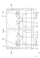
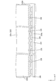
- FIG. Disassembled perspective view of liquid crystal display device An enlarged cross-sectional view in which the vicinity of the LED in the cross section obtained by cutting the liquid crystal display device along the short side direction of the chassis is enlarged.
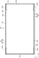
- a plan view of the backlight device viewed from the front side
- the enlarged plan view in which the vicinity of the LED is enlarged in FIG. A plan view schematically showing a path of light incident on a light incident surface
- the top view which looked at the backlight apparatus from the front side in Embodiment 3 The enlarged plan view which expanded LED vicinity in Embodiment 3.
- Embodiment 1 will be described with reference to the drawings.
- the television receiver TV is illustrated.
- a part of each drawing shows an X-axis, a Y-axis, and a Z-axis, and each axis direction is drawn in a common direction in each drawing.
- the Y-axis direction coincides with the vertical direction
- the X-axis direction coincides with the horizontal direction.
- the vertical direction is used as a reference for upper and lower descriptions.
- the television receiver TV includes a liquid crystal display device (an example of a display device) 10, front and back cabinets Ca and Cb that are accommodated so as to sandwich the liquid crystal display device 10, a power source P, a tuner T, and a stand S. ing.
- the liquid crystal display device 10 has a horizontally long rectangular shape as a whole, and includes a liquid crystal panel 16 that is a display panel and a backlight device (an example of an illumination device) 24 that is an external light source, and these form a frame shape.
- the bezel 12 and the like are integrally held.
- the liquid crystal panel 16 is assembled in a posture in which a display surface capable of displaying an image faces the front side.
- the liquid crystal panel 16 has a configuration in which a pair of transparent (highly translucent) glass substrates are bonded together with a predetermined gap therebetween, and a liquid crystal layer (not shown) is sealed between the glass substrates. Is done.
- One glass substrate is provided with a switching element (for example, TFT) connected to a source wiring and a gate wiring orthogonal to each other, a pixel electrode connected to the switching element, an alignment film, and the like.
- the substrate is provided with a color filter and counter electrodes in which colored portions such as R (red), G (green), and B (blue) are arranged in a predetermined arrangement, and an alignment film.
- image data and various control signals necessary for displaying an image are supplied to a source wiring, a gate wiring, a counter electrode, and the like from a drive circuit board (not shown).
- a polarizing plate (not shown) is disposed outside both glass substrates.
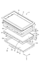
- the backlight device 24 includes a substantially box-shaped chassis 22 that opens toward the front side (light emission side, liquid crystal panel 16 side), a frame 14 disposed on the front side of the chassis 22, And an optical member 18 disposed so as to cover the opening of the frame 14. Further, a pair of LED (Light Emitting Diode) units 32 and 32, four spacers 34, a reflection sheet 26, and a light guide plate 20 are accommodated in the chassis 22. Both side surfaces (light incident surfaces) 20a on the long side of the light guide plate 20 are disposed at positions facing the LED units 32, and guide light emitted from the LED units 32 to the liquid crystal panel 16 side.
- LED Light Emitting Diode
- the optical member 18 is placed on the front side of the light guide plate 20.
- the light guide plate 20 and the optical member 18 are disposed directly below the liquid crystal panel 16 and the LED unit 32 that is a light source is disposed on the side end of the light guide plate 20.
- a so-called edge light system (side light system) is adopted. Below, each component of the backlight apparatus 24 is demonstrated in detail.
- the chassis 22 is made of, for example, a metal plate such as an aluminum plate or an electrogalvanized steel plate (SECC). As shown in FIG. 2, the chassis 22 has a horizontally long bottom plate 22a and both the bottom plate 22a. The side plate 22b rises from each outer edge of the side, and the side plate rises from each outer edge of both short sides of the bottom plate 22a. A space sandwiched between the pair of LED units 32 and 32 in the chassis 22 is a housing space for the light guide plate 20 described later.
- the chassis 22 (bottom plate 22a) has a long side direction that matches the X-axis direction (horizontal direction), and a short side direction that matches the Y-axis direction (vertical direction).
- a projecting portion 22a1 having a frame shape in a plan view projecting toward the light guide plate 20 is provided at an edge portion of the surface of the bottom plate 22a.
- the top surface of the protruding portion 22 is a flat surface, and the light guide plate 20 can be placed along the edge of the spacer 34 via the spacer 34.
- the protruding portion 22a1 supports the light guide plate 20 and the reflection sheet 26 accommodated in the chassis 22 from the back side.
- a control board (not shown) for supplying a driving signal to the liquid crystal panel 16 is attached to the outside of the back side of the bottom plate 22a. Note that other substrates such as an LED driving substrate (not shown) for supplying driving power to the LED unit 32 are attached to the bottom plate 22a in the same manner as the control substrate described above.
- the frame 14 is made of synthetic resin such as plastic, and as shown in FIGS. 2 and 3, the frame 14 is parallel to the optical member 18 and the light guide plate 20 (liquid crystal panel 16) and has a substantially frame shape when viewed in plan. It is comprised from a site
- the substantially frame-shaped portion of the frame 14 extends along the outer peripheral edge portion of the light guide plate 20, and the optical member 18 and the outer peripheral edge portion of the light guide plate 20 arranged on the back side of the frame 14 face the entire surface. It is possible to cover from.
- the substantially frame-shaped portion of the frame 14 can receive (support) the outer peripheral end of the optical member 18 disposed on the front side from the back side over substantially the entire circumference.
- the substantially frame-shaped portion of the frame 14 is disposed so as to be interposed between the optical member 18 and the light guide plate 20.
- one long side portion covers the end portion on the light incident surface 20 a side of the light guide plate 20 and the LED unit 32 collectively from the front side.
- a portion having a substantially short cylindrical shape in the frame 14 is attached in a state of being directed to the outer surface of the side plate 22 b of the chassis 22. The outer surface of the part is arranged in contact with the inner surface of the cylindrical plate surface of the bezel 12 described above.
- the optical member 18 is formed by laminating a diffusion sheet 18a, a lens sheet 18b, and a reflective polarizing plate 18c in order from the light guide plate 20 side.
- the diffusion sheet 18a, the lens sheet 18b, and the reflective polarizing plate 18c have a function of converting light emitted from the LED unit 32 and passing through the light guide plate 20 into planar light.
- the liquid crystal panel 16 is installed on the upper surface side of the reflective polarizing plate 18d, and the optical member 18 is stably disposed in a form sandwiched between the frame 14 and the liquid crystal panel 16. That is, the optical member 18 is slightly larger than the inner edge of the frame 14 and is placed on the surface of the inner edge. Therefore, as shown in the sectional view of FIG. 3, the space formed between the LED 28 and the light guide plate 20 and the end of the optical member 18 are separated by the frame 14.
- the reflection sheet 26 has a rectangular sheet shape, is made of a synthetic resin, and has a white surface with excellent light reflectivity.
- the reflection sheet 26 has a shape in which the long side direction coincides with the X-axis direction, the short side direction coincides with the Y-axis direction, and is sandwiched between the opposite surface 20c of the light guide plate 20 and a spacer 34 described later. (See FIG. 3).
- the reflection sheet 26 has a reflection surface on the front side, and this reflection surface is in contact with the opposite surface 20 c of the light guide plate 20. And the reflection sheet 26 can reflect the light which leaked from the LED unit 32 or the light-guide plate 20 to the reflective surface side.
- the reflection sheet 26 is slightly larger than the opposite surface 20c of the light guide plate 20, and its end edge slightly protrudes from the end portion of the light guide plate 20 as shown in FIGS. ing.
- the four spacers 34 are arranged along the short side direction and the long side direction of the chassis 22 respectively, and have a flat plate shape. Each spacer 34 is placed on the top surface of the protruding portion 22 a 1 of the chassis 22. As described above, the edge of the reflection sheet 26 is sandwiched between the spacers 34 and the light guide plate 20. By sandwiching the reflection sheet in this way, the reflection sheet 26 is fixed, and movement in the plate surface direction of the light guide plate 20 (the plate surface direction of the bottom plate 22a of the chassis 22 and the XY plane direction) is restricted. It has a configuration.
- the pair of LED units 32, 32 are arranged on both long sides of the chassis 22, and are composed of an LED substrate 30 and an LED 28.
- the LED substrate 30 constituting the LED unit 32 is an elongated plate extending along the long side direction of the light guide plate 20 (X-axis direction, long side direction of the light incident surface 20a).
- the plate surface is accommodated in the chassis 22 in a posture parallel to the X-axis direction and the Z-axis direction, that is, a posture parallel to the light incident surface 20a of the light guide plate 20.
- Each LED substrate 30 has a size in the long side direction (X-axis direction) that is approximately the same as the size in the long side direction of the light guide plate 20.
- a plurality of LEDs 28 described below are surface-mounted on the inner side of the LED substrate 30, that is, the plate surface facing the light guide plate 20 side (the surface facing the light guide plate 20).
- the surface 30a On the mounting surface 30a of the LED substrate 30, a wiring pattern (not shown) made of a metal film (such as copper foil) that extends along the X-axis direction and connects the adjacent LEDs 28 across the LED 28 group in series.
- the terminal portions formed at both ends of the wiring pattern are connected to the power supply board via wiring members such as connectors and electric wires so that driving power is supplied to each LED 28. It has become.
- the plate surface opposite to the mounting surface 30 a of the LED substrate 30 is attached to the side plate 22 b on the long side of the chassis 22 by screwing or the like.
- the LED 28 constituting the LED unit 32 is configured such that an LED element (not shown) is sealed with a resin material on a substrate portion fixed to the LED substrate 30.
- the LED element mounted on the substrate portion has one main emission wavelength, and specifically, one that emits blue light in a single color is used.
- a phosphor that emits a predetermined color by being excited by blue light emitted from the LED element is dispersed and mixed, and generally emits white light as a whole. It is said.
- a yellow phosphor that emits yellow light for example, a green phosphor that emits green light, and a red phosphor that emits red light are used in appropriate combination, or any one of them is used. It can be used alone.
- the LED 28 is a so-called top surface light emitting type in which a surface opposite to the mounting surface 30a with respect to the LED substrate 30 (a surface facing the light incident surface 20a of the light guide plate 20) is a main light emitting surface.
- the light guide plate 20 is made of a synthetic resin material (for example, acrylic resin such as PMMA or polycarbonate) having a refractive index sufficiently higher than that of air and almost transparent (excellent translucency).
- the light guide plate 20 has a horizontally long rectangular shape when viewed in plan as in the case of the liquid crystal panel 16 and the chassis 22, and has a plate shape that is thicker than the optical member 18.
- the long side direction in FIG. 4 coincides with the X-axis direction
- the short side direction coincides with the Y-axis direction
- the plate thickness direction perpendicular to the plate surface coincides with the Z-axis direction.
- Both end surfaces on the long side of the light guide plate 20 are light incident surfaces 20a on which light emitted from the LEDs 28 is incident.
- the light incident surface 20a is provided with irregularities 36 to be described later.
- both end surfaces on the short side of the light guide plate 20, that is, both end surfaces adjacent to the light incident surface 20a are adjacent end surfaces 20d.
- the light guide plate 20 has a light incident surface 20a facing the LED unit 32, and a light emitting surface 20b that is a main plate surface (front plate surface) on the optical member 18 side.
- the opposite surface 20c which is the plate surface opposite to the light emitting surface 20b (the plate surface on the back side), is arranged so as to face the reflection sheet 26 side, and a later-described protruding portion of the chassis 22 through the reflection sheet 26 22a1 is supported.
- the alignment direction with the LED unit 32 coincides with the Y-axis direction
- the alignment direction with the optical member 18 and the reflection sheet 26 coincides with the Z-axis direction.
- the light guide plate 20 introduces light emitted from the LED unit 32 along the Y-axis direction from the light incident surface 20a, rises toward the optical member 18 side while propagating the light inside, and emits light. It has the function to emit from 20b.
- the light incident surface 20a of the light guide plate 20 is provided with a plurality of irregularities 36 over the entire surface.
- These irregularities 36 have a prism shape formed such that light emitted from each LED 28 and incident from the light incident surface 20 a is relatively directed to the adjacent end surface 20 d side rather than the center side of the light guide plate 20.
- each of the irregularities 36 extends in a direction orthogonal to the plate surface of the light guide plate 20 (Z-axis direction), and in the center of the light guide plate 20 in a plan view of the light guide plate 20. It is a prism lens that is recessed in a triangular shape.
- the triangular apex portion 36a (see FIG. 6) of the prism lens is formed to be relatively unevenly distributed closer to the adjacent end face 20d.
- the prism lens that forms each of the irregularities 36 has a shape in which the triangular apex portion 36a is unevenly distributed, and as shown in FIG. 6, the two sides that constitute the apex portion 36a.
- the lengths L1 and L4 of the sides relatively positioned on the adjacent end surface 20d side are relatively shorter than the lengths L2 and L3 of the sides positioned on the center side of the light incident surface 20a.
- corrugation 36 provided in the light-incidence surface 20a is made into the above shapes, the light radiate
- the light guide plate 20 spreads toward the adjacent end face 20d side relative to the center side of the light guide plate 20. Thereby, it can suppress that the light from each LED28 overlaps more in the site
- the in-plane luminance distribution on the light emitting surface 20b can be controlled to be substantially uniform in a plan view of the light guide plate 20.
- the light incident from the light incident surface 20a of the light guide plate 20 is directed to the adjacent end surface 20d side by the unevenness 36.
- the lens member or the like is not disposed in the middle of the light path as in the configuration described in the prior art, it is possible to prevent the light utilization efficiency from being lowered.
- the uniformity of the luminance distribution on the light exit surface 20b is improved without reducing the light use efficiency. Can be made.
- each of the irregularities 36 extends in a direction orthogonal to the plate surface of the light guide plate 20 (Z-axis direction) and has a triangular shape toward the center of the light guide plate 20 in a plan view of the light guide plate 20. It is a hollow prism lens, and the triangular apex portion 26a is relatively unevenly distributed closer to the adjacent end face 20d side.
- each of the projections and depressions 36 is relatively light-incident on the side located on the side of the adjacent end face 20d relative to the two sides constituting the triangular apex portion 26a in plan view of the light guide plate 20. The length is shorter than the side located on the center side of the surface 20a.
- corrugation 36 in which the light which injected from the light-incidence surface 20a goes to the adjacent end surface 20d side relatively rather than the center side of the light-guide plate 20 is implement
- the unevenness 36 is provided over the entire surface of the light incident surface 20a. With such a configuration, all the light incident from the light incident surface 20a can be directed to the adjacent end surface 20d side by the unevenness 36, so that the uniformity of the luminance distribution on the light emitting surface 20b is effective. Can be improved.
- the light guide plate 20 is made of synthetic resin. Therefore, when the light guide plate 20 is processed in the manufacturing process, the unevenness 36 can be easily formed on the light incident surface 20a by injection molding or the like.
- the plurality of LEDs 28 are linearly arranged at substantially equal intervals along the light incident surface 20a.
- the LEDs 28 are regularly arranged on the LED substrate 30 and the like, so that compared with the case where the LEDs 28 are irregularly arranged.
- the LED 28 can be easily arranged, and workability in the manufacturing process of the backlight device 24 can be improved.
- each of the irregularities 136 is a prism lens that extends in a direction (Z-axis direction) orthogonal to the plate surface of the light guide plate 120 and projects in a triangular shape toward the outside of the light guide plate 120 in a plan view of the light guide plate 120.
- the apex portion of the triangular shape is relatively unevenly distributed closer to the adjacent end face 120d side.
- Embodiment 3 will be described with reference to the drawings.
- the third embodiment is different from that of the first embodiment in that the unevenness 236 is provided only on a part of the light incident surface 220 a of the light guide plate 220. Since the other configuration is the same as that of the first embodiment, the description of the structure, operation, and effect is omitted.
- FIGS. 8 and 9 the portions obtained by adding the numeral 200 to the reference numerals in FIGS. 4 and 5 are the same as the portions described in the first embodiment.
- the unevenness 236 is provided only in the portion 220 a 1 closer to the adjacent end surface 220 d side of the light incident surface 220 a of the light guide plate 220.
- the shape of the unevenness 236 is the same as that described in the first embodiment.
- the unevenness 236 is provided on the light incident surface 220a in the arrangement as described above, the light incident on the portion of the light incident surface where the unevenness 236 is not provided is on both adjacent end surfaces 220d side. While the light spreads uniformly, the light incident on the portion where the unevenness 236 is provided is directed toward the adjacent end face 220d.
- the unevenness 236 is arranged as in this embodiment, even when the interval between the adjacent LEDs 228 is narrowed, for example, more light overlaps at the center side than at both end sides of the light incident surface 220a. It is possible to prevent the luminance from becoming uneven between the center side and both end sides of the light emitting surface 220b.
- the unevenness 236 is provided only in a portion of the light incident surface 220a that is relatively closer to the adjacent end surface 220d side, so that the unevenness 236 is formed on the entire surface of the light incident surface 220a.
- the processing cost of the light guide plate 220 can be reduced.
- Embodiment 4 will be described with reference to the drawings.
- the density of the unevenness 336 provided on the light incident surface 320a of the light guide plate 320 is different from that of the first embodiment. Since the other configuration is the same as that of the first embodiment, the description of the structure, operation, and effect is omitted.
- FIG. 10 the part obtained by adding the numeral 300 to the reference numeral in FIG. 5 is the same as the part described in the first embodiment.
- the unevenness 336 provided relatively closer to the adjacent end surface 320 d side of the light incident surface 320 a is relatively provided closer to the center side. It is more densely provided. With this configuration, in the present embodiment, more light incident from the adjacent end surface 320d side than the central side of the light incident surface 320a can be directed toward the adjacent end surface 320d. it can. For this reason, the uniformity of the luminance distribution on the light emitting surface 320b can be more effectively improved.
- the television receiver provided with a tuner is exemplified, but the present invention can also be applied to a display device not provided with a tuner.
- TV TV receiver, Ca, Cb: cabinet, T: tuner, S: stand
- 10 liquid crystal display
- 12 bezel
- 14 frame
- 16 liquid crystal panel
- 18 optical member
- 20, 120, 220, 320 Light guide plate, 20a, 120a, 220a, 320a: Light incident surface
- 20b, 120b, 220b, 320b Light exit surface
- 22 Chassis
- 24 Backlight device
- 36a apex angle portion
Abstract
A backlight device comprises a plurality of LEDs (28) disposed in a row; and a light guide plate (20), the long-side end surfaces of which are light incidence surfaces (20a) , and the end surfaces of which adjacent to the light incidence surfaces (20a) are adjacent end surfaces (20d). A plurality of prism-shaped, unevenly profiled portions (36) is formed on the light incidence surfaces (20a) so that the light incident on the light incidence surfaces (20a) is relatively directed to the adjacent end surfaces (20d) rather than the center of the light guide plate (20). The backlight device (24) directs the light incident on the light incidence surfaces (20a) of the light guide plate (20) toward the adjacent end surfaces (20d) via the unevenly profiled portions (36), and thus can suppress a lot of light overlapping on the center instead of on both ends of the light incidence surfaces (20a), and can prevent or suppress an uneven luminance between the center and both ends of the light emission surface (20b).
Description
本発明は、照明装置、表示装置、及びテレビ受信装置に関する。
The present invention relates to a lighting device, a display device, and a television receiver.
例えば、液晶テレビなどの液晶表示装置は、その表示パネルである液晶パネルが自発光しないため、別途に照明装置としてバックライト装置を必要としている。バックライト装置はその機構によって直下型とエッジライト型とに大別されており、液晶表示装置の一層の薄型化を実現するには、エッジライト型のバックライト装置を用いるのが好ましいものとされている。
For example, a liquid crystal display device such as a liquid crystal television requires a backlight device as a separate illumination device because the liquid crystal panel that is the display panel does not emit light. Backlight devices are roughly classified into direct type and edge light type according to the mechanism, and it is preferable to use an edge light type backlight device in order to realize further thinning of the liquid crystal display device. ing.
エッジライト型のバックライト装置では、LED(Light Emitting Diode)等の光源から出射された光を、その一方の板面に設けられた光出射面側へ導光する導光板が筐体内に収容される。導光板には、その少なくとも一つの端面側に光入射面が設けられ、複数の光源が当該光入射面と対向状に配される。
In an edge light type backlight device, a light guide plate that guides light emitted from a light source such as an LED (Light Emitting Diode) to a light emitting surface provided on one of the plate surfaces is accommodated in the housing. The The light guide plate is provided with a light incident surface on at least one end surface side thereof, and a plurality of light sources are arranged to face the light incident surface.
ところで、バックライト装置では、デザイン上の理由等によって当該バックライト装置の額縁部分を狭くする、いわゆる狭額縁化が要求されることがある。狭額縁化が図られたバックライト装置では、狭額縁化が図られていないバックライト装置と比べて光源と表示面における表示領域との間の距離が短いものとされる。この場合、光入射面と対向状に配された複数のLEDから出射される光の像が表示面において視認され易くなる現象が発生する。狭額縁化が図られたバックライト装置においてこの現象を回避するためには、複数のLEDの間隔を狭めることが有効とされる。
By the way, in the backlight device, there is a case where the so-called narrow frame is required to narrow the frame portion of the backlight device for a design reason or the like. In the backlight device in which the frame is narrowed, the distance between the light source and the display area on the display surface is shorter than that in the backlight device in which the frame is not narrowed. In this case, a phenomenon occurs in which images of light emitted from a plurality of LEDs arranged to face the light incident surface are easily visible on the display surface. In order to avoid this phenomenon in a backlight device with a narrow frame, it is effective to reduce the interval between a plurality of LEDs.
その一方、複数のLEDの間隔を狭めると、各LEDから出射される光が導光板の光入射面の端側よりも中央側において多く重なり合うため、光入射面の端側における光量が中央側よりも不足する。これにより、当該バックライト装置において表示面の端側が中央側よりも相対的に暗くなり、表示面における輝度分布が不均一となることがある。このような表示面における輝度分布の不均一を解消することを目的としたバックライトユニットが、例えば特許文献1に開示されている。
On the other hand, if the interval between the plurality of LEDs is narrowed, the light emitted from each LED overlaps more on the center side than on the end side of the light incident surface of the light guide plate. Is also lacking. Thereby, in the backlight device, the end side of the display surface may be relatively darker than the center side, and the luminance distribution on the display surface may be uneven. For example, Patent Literature 1 discloses a backlight unit that aims to eliminate such uneven luminance distribution on the display surface.
(発明が解決しようとする課題)
しかしながら、上記特許文献1のバックライトユニットでは、導光板と表示面との間に表示面全体の輝度分布を均一に制御することができる光学シートを配することで、表示面における輝度分布の不均一を解消する。この光学シートは、略半球状の複数のレンズと、複数配列された連続する幾何学構造体と、を併せ持つ構成とされている。このため、光学シートを通過する光の経路が長いものとなり、光の利用効率が低下する問題があった。 (Problems to be solved by the invention)
However, in the backlight unit disclosed in Patent Document 1, an optical sheet that can uniformly control the luminance distribution of the entire display surface is disposed between the light guide plate and the display surface, thereby reducing the luminance distribution on the display surface. Eliminate uniformity. This optical sheet is configured to have a plurality of substantially hemispherical lenses and a plurality of continuous geometric structures arranged in series. For this reason, the path | route of the light which passes an optical sheet becomes a long thing, and there existed a problem that the utilization efficiency of light fell.
本明細書で開示される技術は、上記の課題に鑑みて創作されたものである。本明細書で開示では、光の利用効率を低下させることなく、表示面における輝度分布の均一性を向上させることが可能な技術を提供することを目的とする。
The technology disclosed in this specification has been created in view of the above problems. An object of the present disclosure is to provide a technique capable of improving the uniformity of the luminance distribution on the display surface without reducing the light use efficiency.
(課題を解決するための手段)
本明細書で開示される技術は、列をなして複数配置されたLEDと、少なくとも一つの端面が前記複数のLEDからの光が入射される光入射面とされ、該光入射面と隣り合う端面が隣接端面とされた導光板であって、前記光入射面に、該光入射面から入射した光が該導光板の中央側よりも相対的に前記隣接端面側に向かうように成形されたプリズム形状の複数の凹凸が設けられた導光板と、を備える照明装置に関する。 (Means for solving the problem)
In the technology disclosed in this specification, a plurality of LEDs arranged in a row, and at least one end surface is a light incident surface on which light from the plurality of LEDs is incident, and are adjacent to the light incident surface. A light guide plate whose end face is an adjacent end face, and is formed on the light incident surface so that light incident from the light incident surface is directed toward the adjacent end face side relative to the center side of the light guide plate. And a light guide plate provided with a plurality of prism-shaped projections and depressions.
上記の照明装置によると、導光板の光入射面から入射した光が凹凸によって隣接端面側に向かうため、例えば隣り合うLEDの間隔が狭められた場合でも、光入射面の端側よりも中央側において多くの光が重なり合うことを抑制することができ、表示面の中央側と端側との間で輝度が不均一となることを防止ないし抑制することができる。また、従来技術で述べた構成のように光の経路の途中にレンズ部材等が配されることがないため、光の利用効率が低下することを防止することもできる。その結果、上記の照明装置では、隣り合うLEDの間隔が狭められた場合であっても、光の利用効率を低下させることなく、表示面における輝度分布の均一性を向上させることができる。
According to the illuminating device described above, the light incident from the light incident surface of the light guide plate is directed toward the adjacent end surface due to the unevenness. For example, even when the interval between adjacent LEDs is narrowed, for example, the center side of the light incident surface. In this case, it is possible to prevent a large amount of light from overlapping with each other, and it is possible to prevent or suppress the luminance from becoming uneven between the center side and the end side of the display surface. Further, since the lens member or the like is not disposed in the middle of the light path as in the configuration described in the prior art, it is possible to prevent the light utilization efficiency from being lowered. As a result, in the above illumination device, even when the interval between adjacent LEDs is narrowed, the uniformity of the luminance distribution on the display surface can be improved without reducing the light use efficiency.
前記凹凸の各々は、前記導光板の板面と直交する方向に延びるとともに、該導光板の平面視において該導光板の中央側に向かって三角形状に窪んだプリズムレンズであって、前記三角形状の頂角部が相対的に前記隣接端面側寄りに偏在する形状とされていてもよい。
この構成によると、光入射面から入射した光が導光板の中央側よりも相対的に隣接端面側に向かうような凹凸の具体的な形状を提供することができる。 Each of the irregularities is a prism lens extending in a direction orthogonal to the plate surface of the light guide plate and recessed in a triangular shape toward the center of the light guide plate in a plan view of the light guide plate. The apex angle portion may be relatively unevenly distributed closer to the adjacent end face side.
According to this configuration, it is possible to provide a specific shape of unevenness in which light incident from the light incident surface is directed toward the adjacent end surface side relatively than the center side of the light guide plate.
前記凹凸の各々は、前記導光板の板面と直交する方向に延びるとともに、該導光板の平面視において該導光板の外側に向かって三角形状に突出したプリズムレンズであって、前記三角形状の頂角部が相対的に前記隣接端面側寄りに偏在する形状とされていてもよい。
この構成によると、光入射面から入射した光が導光板の中央側よりも相対的に隣接端面側に向かうような凹凸の具体的な形状を提供することができる。 Each of the concaves and convexes is a prism lens that extends in a direction orthogonal to the plate surface of the light guide plate and protrudes in a triangular shape toward the outside of the light guide plate in a plan view of the light guide plate. The apex angle portion may have a shape that is relatively unevenly distributed closer to the adjacent end surface.
According to this configuration, it is possible to provide a specific shape of unevenness in which light incident from the light incident surface is directed toward the adjacent end surface side relatively than the center side of the light guide plate.
前記凹凸の各々は、前記導光板の平面視において、前記三角形状の前記頂角部を構成する二辺について、相対的に前記隣接端面側に位置する辺が相対的に前記光入射面の中央側に位置する辺よりも短いものとされていてもよい。
この構成によると、光入射面から入射した光が導光板の中央側よりも相対的に隣接端面側に向かうような凹凸の具体的な形状を提供することができる。 Each of the irregularities has a side relatively located on the side of the adjacent end surface relative to the two sides constituting the apex angle portion of the triangle in a plan view of the light guide plate. It may be shorter than the side located on the side.
According to this configuration, it is possible to provide a specific shape of unevenness in which light incident from the light incident surface is directed toward the adjacent end surface side relatively than the center side of the light guide plate.
前記凹凸は、前記光入射面の全面に亘って設けられていてもよい。
この構成によると、光入射面から入射した全ての光を凹凸によって隣接端面側に向かわせることができるため、表示面における輝度分布の均一性を効果的に向上させることができる。 The unevenness may be provided over the entire surface of the light incident surface.
According to this configuration, since all the light incident from the light incident surface can be directed toward the adjacent end surface by the unevenness, the uniformity of the luminance distribution on the display surface can be effectively improved.
前記光入射面のうち相対的に前記隣接端面側寄りに設けられた前記凹凸が相対的に中央側寄りに設けられた前記凹凸よりも密に設けられていてもよい。
この構成によると、光入射面のうちその中央側よりも相対的に隣接端面側から入射した光をより多く隣接端面側へ向かわせることができる。このため、表示面における輝度分布の均一性をより効果的に向上させることができる。 The unevenness provided relatively closer to the adjacent end surface of the light incident surface may be provided more densely than the unevenness provided relatively closer to the center.
According to this configuration, it is possible to direct more light incident from the adjacent end surface side toward the adjacent end surface side than the center side of the light incident surface. For this reason, the uniformity of the luminance distribution on the display surface can be improved more effectively.
前記凹凸は、前記光入射面のうち相対的に前記隣接端面側寄りの部位にのみ設けられていてもよい。
この構成によると、凹凸を光入射面の全面に形成する場合と比べて導光板の加工コストを削減することができる。 The unevenness may be provided only in a portion of the light incident surface that is relatively closer to the adjacent end surface.
According to this configuration, the processing cost of the light guide plate can be reduced as compared with the case where the unevenness is formed on the entire surface of the light incident surface.
前記導光板は樹脂製であってもよい。
この構成によると、製造工程において導光板を加工する際、射出成形等によって光入射面に容易に凹凸を形成することができる。 The light guide plate may be made of resin.
According to this configuration, when the light guide plate is processed in the manufacturing process, the unevenness can be easily formed on the light incident surface by injection molding or the like.
前記複数のLEDは、前記光入射面に沿って直線状に略等間隔で配置されていてもよい。
この構成によると、照明装置の製造工程においてLEDがLED基板上等に規則的に配置されることとなるため、LEDが不規則に配置される場合と比べてLEDを配置し易いものとすることができ、照明装置の製造工程における作業性を高めることができる。 The plurality of LEDs may be linearly arranged at substantially equal intervals along the light incident surface.
According to this configuration, since the LEDs are regularly arranged on the LED substrate or the like in the manufacturing process of the lighting device, it is easier to arrange the LEDs than when the LEDs are irregularly arranged. Therefore, workability in the manufacturing process of the lighting device can be improved.
本明細書で開示される技術は、上記の照明装置と、上記の照明装置からの光を利用して表示を行う表示パネルと、を備える表示装置として表現することもできる。また、当該表示パネルを、液晶を用いた液晶パネルとする表示装置も、新規で有用である。また、上記の表示装置を備えるテレビ受信装置も、新規で有用である。
The technology disclosed in this specification can also be expressed as a display device including the above-described lighting device and a display panel that performs display using light from the lighting device. A display device in which the display panel is a liquid crystal panel using liquid crystal is also new and useful. A television receiver provided with the above display device is also new and useful.
(発明の効果)
本明細書で開示される技術によれば、光の利用効率を低下させることなく、表示面における輝度分布の均一性を向上させることができる。 (The invention's effect)
According to the technology disclosed in this specification, the uniformity of the luminance distribution on the display surface can be improved without reducing the light utilization efficiency.
本明細書で開示される技術によれば、光の利用効率を低下させることなく、表示面における輝度分布の均一性を向上させることができる。 (The invention's effect)
According to the technology disclosed in this specification, the uniformity of the luminance distribution on the display surface can be improved without reducing the light utilization efficiency.
<実施形態1>
図面を参照して実施形態1を説明する。本実施形態ではテレビ受信装置TVについて例示する。なお、各図面の一部にはX軸、Y軸およびZ軸を示しており、各軸方向が各図面で共通した方向となるように描かれている。このうちY軸方向は、鉛直方向と一致し、X軸方向は、水平方向と一致している。また、特に断りがない限りは、上下の記載については鉛直方向を基準とする。 <Embodiment 1>
Embodiment 1 will be described with reference to the drawings. In the present embodiment, the television receiver TV is illustrated. A part of each drawing shows an X-axis, a Y-axis, and a Z-axis, and each axis direction is drawn in a common direction in each drawing. Among these, the Y-axis direction coincides with the vertical direction, and the X-axis direction coincides with the horizontal direction. In addition, unless otherwise noted, the vertical direction is used as a reference for upper and lower descriptions.
テレビ受信装置TVは、液晶表示装置(表示装置の一例)10と、当該液晶表示装置10を挟むようにして収容する表裏両キャビネットCa、Cbと、電源Pと、チューナーTと、スタンドSと、を備えている。液晶表示装置10は、全体として横長の方形を成しており、表示パネルである液晶パネル16と、外部光源であるバックライト装置(照明装置の一例)24とを備え、これらが枠状を成すベゼル12などにより一体的に保持されるようになっている。液晶表示装置10において液晶パネル16は、画像を表示可能な表示面が表側を向いた姿勢で組み付けられている。
The television receiver TV includes a liquid crystal display device (an example of a display device) 10, front and back cabinets Ca and Cb that are accommodated so as to sandwich the liquid crystal display device 10, a power source P, a tuner T, and a stand S. ing. The liquid crystal display device 10 has a horizontally long rectangular shape as a whole, and includes a liquid crystal panel 16 that is a display panel and a backlight device (an example of an illumination device) 24 that is an external light source, and these form a frame shape. The bezel 12 and the like are integrally held. In the liquid crystal display device 10, the liquid crystal panel 16 is assembled in a posture in which a display surface capable of displaying an image faces the front side.
続いて、液晶パネル16について説明する。液晶パネル16は、透明な(高い透光性を有する)一対のガラス基板が所定のギャップを隔てた状態で貼り合わせられるとともに、両ガラス基板間に液晶層(図示しない)が封入された構成とされる。一方のガラス基板には、互いに直交するソース配線とゲート配線とに接続されたスイッチング素子(例えばTFT)と、そのスイッチング素子に接続された画素電極、さらには配向膜等が設けられ、他方のガラス基板には、R(赤色),G(緑色),B(青色)等の各着色部が所定配列で配置されたカラーフィルタや対向電極、さらには配向膜等が設けられている。このうち、ソース配線、ゲート配線および対向電極などには、図示しない駆動回路基板から画像を表示するのに必要な画像データや各種制御信号が供給されるようになっている。なお、両ガラス基板の外側には偏光板(図示しない)が配されている。
Subsequently, the liquid crystal panel 16 will be described. The liquid crystal panel 16 has a configuration in which a pair of transparent (highly translucent) glass substrates are bonded together with a predetermined gap therebetween, and a liquid crystal layer (not shown) is sealed between the glass substrates. Is done. One glass substrate is provided with a switching element (for example, TFT) connected to a source wiring and a gate wiring orthogonal to each other, a pixel electrode connected to the switching element, an alignment film, and the like. The substrate is provided with a color filter and counter electrodes in which colored portions such as R (red), G (green), and B (blue) are arranged in a predetermined arrangement, and an alignment film. Of these, image data and various control signals necessary for displaying an image are supplied to a source wiring, a gate wiring, a counter electrode, and the like from a drive circuit board (not shown). A polarizing plate (not shown) is disposed outside both glass substrates.
続いて、バックライト装置24について説明する。図2に示すように、バックライト装置24は、表側(光出射側、液晶パネル16側)に向けて開口する略箱型をなすシャーシ22と、シャーシ22の表側に配されたフレーム14と、フレーム14の開口を覆うようにして配される光学部材18とを備える。さらに、シャーシ22内には、一対のLED(Light Emitting Diode)ユニット32,32と、4つのスペーサ34と、反射シート26と、導光板20とが収容されている。導光板20の長辺側における両側面(光入射面)20aは、各LEDユニット32と対向する位置に配されており、当該LEDユニット32から出射される光を液晶パネル16側へ導く。そして、この導光板20の表側に光学部材18が載置されている。本実施形態に係るバックライト装置24では、導光板20および光学部材18が液晶パネル16の直下に配されていると共に光源であるLEDユニット32が導光板20の側端部に配されてなる、いわゆるエッジライト方式(サイドライト方式)を採用している。以下では、バックライト装置24の各構成部品について詳しく説明する。
Subsequently, the backlight device 24 will be described. As shown in FIG. 2, the backlight device 24 includes a substantially box-shaped chassis 22 that opens toward the front side (light emission side, liquid crystal panel 16 side), a frame 14 disposed on the front side of the chassis 22, And an optical member 18 disposed so as to cover the opening of the frame 14. Further, a pair of LED (Light Emitting Diode) units 32 and 32, four spacers 34, a reflection sheet 26, and a light guide plate 20 are accommodated in the chassis 22. Both side surfaces (light incident surfaces) 20a on the long side of the light guide plate 20 are disposed at positions facing the LED units 32, and guide light emitted from the LED units 32 to the liquid crystal panel 16 side. The optical member 18 is placed on the front side of the light guide plate 20. In the backlight device 24 according to the present embodiment, the light guide plate 20 and the optical member 18 are disposed directly below the liquid crystal panel 16 and the LED unit 32 that is a light source is disposed on the side end of the light guide plate 20. A so-called edge light system (side light system) is adopted. Below, each component of the backlight apparatus 24 is demonstrated in detail.
シャーシ22は、例えばアルミニウム板や電気亜鉛めっき鋼板(SECC)などの金属板からなり、図2に示すように、液晶パネル16と同様に横長の方形状をなす底板22aと、底板22aの両長辺の各外縁から立ち上がる側板22bと、底板22aの両短辺の各外縁から立ち上がる側板とから構成されている。シャーシ22内において一対のLEDユニット32,32の間に挟まれた空間が、後述する導光板20用の収容空間となっている。シャーシ22(底板22a)は、その長辺方向がX軸方向(水平方向)と一致し、短辺方向がY軸方向(鉛直方向)と一致している。また、底板22aの表面の端縁部には導光板20側に向かって突出する平面視枠状の突出部位22a1が設けられている。突出部位22の頂面は平坦面となっており、スペーサ34を介して導光板20をその端縁に沿って載置することが可能となっている。突出部位22a1は、シャーシ22内に収容された導光板20及び反射シート26を裏側から支持している。底板22aの裏側外部には、液晶パネル16に駆動のための信号を供給する図示しないコントロール基板が取り付けられている。なお、底板22aには、上記したコントロール基板と同様にして、LEDユニット32に駆動電力を供給する図示しないLED駆動基板などの他の基板類が取り付けられている。
The chassis 22 is made of, for example, a metal plate such as an aluminum plate or an electrogalvanized steel plate (SECC). As shown in FIG. 2, the chassis 22 has a horizontally long bottom plate 22a and both the bottom plate 22a. The side plate 22b rises from each outer edge of the side, and the side plate rises from each outer edge of both short sides of the bottom plate 22a. A space sandwiched between the pair of LED units 32 and 32 in the chassis 22 is a housing space for the light guide plate 20 described later. The chassis 22 (bottom plate 22a) has a long side direction that matches the X-axis direction (horizontal direction), and a short side direction that matches the Y-axis direction (vertical direction). Further, a projecting portion 22a1 having a frame shape in a plan view projecting toward the light guide plate 20 is provided at an edge portion of the surface of the bottom plate 22a. The top surface of the protruding portion 22 is a flat surface, and the light guide plate 20 can be placed along the edge of the spacer 34 via the spacer 34. The protruding portion 22a1 supports the light guide plate 20 and the reflection sheet 26 accommodated in the chassis 22 from the back side. A control board (not shown) for supplying a driving signal to the liquid crystal panel 16 is attached to the outside of the back side of the bottom plate 22a. Note that other substrates such as an LED driving substrate (not shown) for supplying driving power to the LED unit 32 are attached to the bottom plate 22a in the same manner as the control substrate described above.
フレーム14は、プラスチック等の合成樹脂製とされており、図2及び図3に示すように、光学部材18及び導光板20(液晶パネル16)に並行するとともに平面に視て略枠状をなす部位と、当該部位の外周縁部から裏側に向けて突出するとともに略短筒状をなす部位とから構成される。フレーム14における略枠状をなす部位は、導光板20の外周縁部に沿って延在しており、その裏側に配される光学部材18及び導光板20の外周縁部をほぼ全周にわたって表側から覆うことが可能とされる。その一方で、フレーム14における略枠状をなす部位は、その表側に配される光学部材18における外周端部をほぼ全周にわたって裏側から受ける(支持する)ことができる。つまり、フレーム14における略枠状をなす部位は、光学部材18と導光板20との間に介在する形で配されている。また、フレーム14における略枠状をなす部位において、一方の長辺部分は、導光板20の光入射面20a側の端部とLEDユニット32とを一括して表側から覆うものとされる。フレーム14における略短筒状をなす部位は、シャーシ22の側板22bにおける外面に宛てがわれた状態で取り付けられている。当該部位の外面は、上述したベゼル12の筒状の板面における内面と当接した形で配されている。
The frame 14 is made of synthetic resin such as plastic, and as shown in FIGS. 2 and 3, the frame 14 is parallel to the optical member 18 and the light guide plate 20 (liquid crystal panel 16) and has a substantially frame shape when viewed in plan. It is comprised from a site | part and the site | part which makes a substantially short cylinder shape while projecting toward the back side from the outer periphery part of the said site | part. The substantially frame-shaped portion of the frame 14 extends along the outer peripheral edge portion of the light guide plate 20, and the optical member 18 and the outer peripheral edge portion of the light guide plate 20 arranged on the back side of the frame 14 face the entire surface. It is possible to cover from. On the other hand, the substantially frame-shaped portion of the frame 14 can receive (support) the outer peripheral end of the optical member 18 disposed on the front side from the back side over substantially the entire circumference. In other words, the substantially frame-shaped portion of the frame 14 is disposed so as to be interposed between the optical member 18 and the light guide plate 20. In addition, in a portion having a substantially frame shape in the frame 14, one long side portion covers the end portion on the light incident surface 20 a side of the light guide plate 20 and the LED unit 32 collectively from the front side. A portion having a substantially short cylindrical shape in the frame 14 is attached in a state of being directed to the outer surface of the side plate 22 b of the chassis 22. The outer surface of the part is arranged in contact with the inner surface of the cylindrical plate surface of the bezel 12 described above.
光学部材18は、導光板20側から順に、拡散シート18a、レンズシート18b、反射型偏光板18cが積層されたものである。拡散シート18a、レンズシート18b、反射型偏光板18cは、LEDユニット32から出射され、導光板20を通過した光を面状の光とする機能を有している。反射型偏光板18dの上面側には液晶パネル16が設置されており、光学部材18はフレーム14と液晶パネル16との間に挟持された形で安定して配されている。即ち、光学部材18は、フレーム14の内縁よりも一回り大きいものとされ、当該内縁の表面上に載置されている。従って、図3の断面図に示すように、LED28と導光板20との間に形成された空間と、光学部材18の端部と、の間はフレーム14によって隔てられた構成となっている。
The optical member 18 is formed by laminating a diffusion sheet 18a, a lens sheet 18b, and a reflective polarizing plate 18c in order from the light guide plate 20 side. The diffusion sheet 18a, the lens sheet 18b, and the reflective polarizing plate 18c have a function of converting light emitted from the LED unit 32 and passing through the light guide plate 20 into planar light. The liquid crystal panel 16 is installed on the upper surface side of the reflective polarizing plate 18d, and the optical member 18 is stably disposed in a form sandwiched between the frame 14 and the liquid crystal panel 16. That is, the optical member 18 is slightly larger than the inner edge of the frame 14 and is placed on the surface of the inner edge. Therefore, as shown in the sectional view of FIG. 3, the space formed between the LED 28 and the light guide plate 20 and the end of the optical member 18 are separated by the frame 14.
反射シート26は、長方形のシート状を成し、合成樹脂製とされると共にその表面が光反射性に優れた白色とされている。反射シート26は、その長辺方向がX軸方向と一致し、その短辺方向がY軸方向と一致するとともに、導光板20の反対面20cと後述するスペーサ34との間に挟持された形で配されている(図3参照)。反射シート26は、その表側に反射面を有し、この反射面が導光板20の反対面20cと当接している。そして、反射シート26は、LEDユニット32又は導光板20からその反射面側へ漏れた光を反射させることが可能となっている。また、反射シート26は、導光板20の反対面20cよりも一回り大きいものとされ、図2及び図3に示すように、その端縁が導光板20の端部よりわずかにはみ出すものとされている。
The reflection sheet 26 has a rectangular sheet shape, is made of a synthetic resin, and has a white surface with excellent light reflectivity. The reflection sheet 26 has a shape in which the long side direction coincides with the X-axis direction, the short side direction coincides with the Y-axis direction, and is sandwiched between the opposite surface 20c of the light guide plate 20 and a spacer 34 described later. (See FIG. 3). The reflection sheet 26 has a reflection surface on the front side, and this reflection surface is in contact with the opposite surface 20 c of the light guide plate 20. And the reflection sheet 26 can reflect the light which leaked from the LED unit 32 or the light-guide plate 20 to the reflective surface side. The reflection sheet 26 is slightly larger than the opposite surface 20c of the light guide plate 20, and its end edge slightly protrudes from the end portion of the light guide plate 20 as shown in FIGS. ing.
4つのスペーサ34は、シャーシ22の両短辺方向及び両長辺方向に沿うようにそれぞれ配されており、平板状をなしている。各スペーサ34は、シャーシ22の突出部位22a1の頂面上に載置されている。そして、上述したように反射シート26の端縁部は、各スペーサ34と導光板20との間に挟持された状態となっている。このように反射シートが挟持されることで当該反射シート26は固定され、導光板20の板面方向(シャーシ22の底板22aの板面方向、X-Y平面方向)への移動が規制される構成となっている。なお、反射シート26の外端部の一部をスペーサ34と導光板20との間に挟持されない構成とすることで、当該外端部の一部を導光板20の板面方向への移動が許容されるものとし、これにより、熱膨張等により反射シート26に生じた皺を当該外端部の一部で解消させることができるものとしてもよい。
The four spacers 34 are arranged along the short side direction and the long side direction of the chassis 22 respectively, and have a flat plate shape. Each spacer 34 is placed on the top surface of the protruding portion 22 a 1 of the chassis 22. As described above, the edge of the reflection sheet 26 is sandwiched between the spacers 34 and the light guide plate 20. By sandwiching the reflection sheet in this way, the reflection sheet 26 is fixed, and movement in the plate surface direction of the light guide plate 20 (the plate surface direction of the bottom plate 22a of the chassis 22 and the XY plane direction) is restricted. It has a configuration. It should be noted that a part of the outer end portion of the reflection sheet 26 is not sandwiched between the spacer 34 and the light guide plate 20, so that a part of the outer end portion is moved in the plate surface direction of the light guide plate 20. As a result, the wrinkles generated in the reflection sheet 26 due to thermal expansion or the like may be eliminated by a part of the outer end portion.
一対のLEDユニット32,32は、シャーシ22の両長辺側にそれぞれ配されており、LED基板30とLED28とから構成されている。LEDユニット32を構成するLED基板30は、図2及び図4に示すように、導光板20の長辺方向(X軸方向、光入射面20aの長辺方向)に沿って延在する細長い板状をなしており、その板面をX軸方向及びZ軸方向に並行した姿勢、つまり導光板20の光入射面20aに並行した姿勢でシャーシ22内に収容されている。各LED基板30は、その長辺方向(X軸方向)の寸法が導光板20の長辺方向の寸法と同程度の大きさとされている。LED基板30の板面であって内側、つまり導光板20側を向いた板面(導光板20との対向面)には、次述する複数のLED28が表面実装されており、この面が実装面30aとされる。LED基板30の実装面30aには、X軸方向に沿って延在するとともにLED28群を横切って隣り合うLED28同士を直列接続する、金属膜(銅箔など)からなる配線パターン(図示せず)が形成されており、この配線パターンの両端部に形成された端子部が、コネクタや電線などの配線部材を介して電源基板に接続されることで、各LED28に駆動電力が供給されるようになっている。LED基板30の実装面30aとは反対側の板面は、シャーシ22の長辺側の側板22bにビス留め等により取り付けられている。
The pair of LED units 32, 32 are arranged on both long sides of the chassis 22, and are composed of an LED substrate 30 and an LED 28. As shown in FIGS. 2 and 4, the LED substrate 30 constituting the LED unit 32 is an elongated plate extending along the long side direction of the light guide plate 20 (X-axis direction, long side direction of the light incident surface 20a). The plate surface is accommodated in the chassis 22 in a posture parallel to the X-axis direction and the Z-axis direction, that is, a posture parallel to the light incident surface 20a of the light guide plate 20. Each LED substrate 30 has a size in the long side direction (X-axis direction) that is approximately the same as the size in the long side direction of the light guide plate 20. A plurality of LEDs 28 described below are surface-mounted on the inner side of the LED substrate 30, that is, the plate surface facing the light guide plate 20 side (the surface facing the light guide plate 20). The surface 30a. On the mounting surface 30a of the LED substrate 30, a wiring pattern (not shown) made of a metal film (such as copper foil) that extends along the X-axis direction and connects the adjacent LEDs 28 across the LED 28 group in series. The terminal portions formed at both ends of the wiring pattern are connected to the power supply board via wiring members such as connectors and electric wires so that driving power is supplied to each LED 28. It has become. The plate surface opposite to the mounting surface 30 a of the LED substrate 30 is attached to the side plate 22 b on the long side of the chassis 22 by screwing or the like.
LEDユニット32を構成するLED28は、LED基板30に固着される基板部上にLED素子(図示せず)を樹脂材により封止した構成とされる。基板部に実装されるLED素子は、主発光波長が1種類とされ、具体的には、青色を単色発光するものが用いられている。その一方、LED素子を封止する樹脂パッケージには、LED素子から発せられた青色の光により励起されて所定の色を発光する蛍光体が分散配合されており、全体として概ね白色光を発するものとされる。なお、蛍光体としては、例えば黄色光を発光する黄色蛍光体、緑色光を発光する緑色蛍光体、及び赤色光を発光する赤色蛍光体の中から適宜組み合わせて用いたり、またはいずれか1つを単独で用いたりすることができる。このLED28は、LED基板30に対する実装面30aとは反対側の面(導光板20の光入射面20aと対向する面)が主発光面となる、いわゆる頂面発光型とされている。
The LED 28 constituting the LED unit 32 is configured such that an LED element (not shown) is sealed with a resin material on a substrate portion fixed to the LED substrate 30. The LED element mounted on the substrate portion has one main emission wavelength, and specifically, one that emits blue light in a single color is used. On the other hand, in the resin package for sealing the LED element, a phosphor that emits a predetermined color by being excited by blue light emitted from the LED element is dispersed and mixed, and generally emits white light as a whole. It is said. In addition, as the phosphor, for example, a yellow phosphor that emits yellow light, a green phosphor that emits green light, and a red phosphor that emits red light are used in appropriate combination, or any one of them is used. It can be used alone. The LED 28 is a so-called top surface light emitting type in which a surface opposite to the mounting surface 30a with respect to the LED substrate 30 (a surface facing the light incident surface 20a of the light guide plate 20) is a main light emitting surface.
導光板20は、屈折率が空気よりも十分に高く且つほぼ透明な(透光性に優れた)合成樹脂材料(例えばPMMAなどのアクリル樹脂やポリカーボネイトなど)からなる。導光板20は、図2に示すように、液晶パネル16及びシャーシ22と同様に平面に視て横長の方形状をなすとともに光学部材18よりも厚みが大きな板状をなしており、その板面における長辺方向がX軸方向と、短辺方向がY軸方向とそれぞれ一致し、且つ板面と直交する板厚方向がZ軸方向と一致している。導光板20の長辺側における両端面は、LED28から出射された光が入射する光入射面20aとされている。この光入射面20aには、後述する凹凸36が設けられている。また、図4に示すように、導光板20の短辺側における両端面、即ち光入射面20aと隣り合う両端面は、隣接端面20dとされている。
The light guide plate 20 is made of a synthetic resin material (for example, acrylic resin such as PMMA or polycarbonate) having a refractive index sufficiently higher than that of air and almost transparent (excellent translucency). As shown in FIG. 2, the light guide plate 20 has a horizontally long rectangular shape when viewed in plan as in the case of the liquid crystal panel 16 and the chassis 22, and has a plate shape that is thicker than the optical member 18. The long side direction in FIG. 4 coincides with the X-axis direction, the short side direction coincides with the Y-axis direction, and the plate thickness direction perpendicular to the plate surface coincides with the Z-axis direction. Both end surfaces on the long side of the light guide plate 20 are light incident surfaces 20a on which light emitted from the LEDs 28 is incident. The light incident surface 20a is provided with irregularities 36 to be described later. As shown in FIG. 4, both end surfaces on the short side of the light guide plate 20, that is, both end surfaces adjacent to the light incident surface 20a are adjacent end surfaces 20d.
導光板20は、図2及び図3に示すように、光入射面20aをLEDユニット32と対向させた形で、主板面(表側の板面)である光出射面20bを光学部材18側に向け、光出射面20bとは反対側の板面(裏側の板面)である反対面20cを反射シート26側に向ける形で配され、当該反射シート26を介してシャーシ22の後述する突出部位22a1によって支持されている。導光板20は、LEDユニット32との並び方向がY軸方向と一致しており、光学部材18及び反射シート26との並び方向がZ軸方向と一致するものとされる。導光板20は、LEDユニット32からY軸方向に沿って発せられた光を光入射面20aから導入するとともに、その光を内部で伝播させつつ光学部材18側へ向くよう立ち上げて光出射面20bから出射させる機能を有する。
2 and 3, the light guide plate 20 has a light incident surface 20a facing the LED unit 32, and a light emitting surface 20b that is a main plate surface (front plate surface) on the optical member 18 side. The opposite surface 20c, which is the plate surface opposite to the light emitting surface 20b (the plate surface on the back side), is arranged so as to face the reflection sheet 26 side, and a later-described protruding portion of the chassis 22 through the reflection sheet 26 22a1 is supported. In the light guide plate 20, the alignment direction with the LED unit 32 coincides with the Y-axis direction, and the alignment direction with the optical member 18 and the reflection sheet 26 coincides with the Z-axis direction. The light guide plate 20 introduces light emitted from the LED unit 32 along the Y-axis direction from the light incident surface 20a, rises toward the optical member 18 side while propagating the light inside, and emits light. It has the function to emit from 20b.
導光板20の光入射面20aには、図5に示すように、その全面に亘って複数の凹凸36が設けられている。これらの凹凸36は、各LED28から出射されて光入射面20aから入射した光が導光板20の中央側よりも相対的に隣接端面20d側に向かうように成形されたプリズム形状とされている。具体的には、凹凸36の各々は、図5に示すように、導光板20の板面と直交する方向(Z軸方向)に延びるとともに、導光板20の平面視において導光板20の中央側に向かって三角形状に窪んだプリズムレンズとされている。そして、このプリズムレンズの三角形状の頂角部36a(図6参照)が相対的に隣接端面20d寄りに偏在する形状とされている。
As shown in FIG. 5, the light incident surface 20a of the light guide plate 20 is provided with a plurality of irregularities 36 over the entire surface. These irregularities 36 have a prism shape formed such that light emitted from each LED 28 and incident from the light incident surface 20 a is relatively directed to the adjacent end surface 20 d side rather than the center side of the light guide plate 20. Specifically, as shown in FIG. 5, each of the irregularities 36 extends in a direction orthogonal to the plate surface of the light guide plate 20 (Z-axis direction), and in the center of the light guide plate 20 in a plan view of the light guide plate 20. It is a prism lens that is recessed in a triangular shape. The triangular apex portion 36a (see FIG. 6) of the prism lens is formed to be relatively unevenly distributed closer to the adjacent end face 20d.
上述したように各凹凸36を構成するプリズムレンズが、その三角形状の頂角部36aが偏在する形状とされていることで、図6に示すように、当該頂角部36aを構成する二辺について、相対的に隣接端面20d側に位置する辺の長さL1、L4が相対的に光入射面20aの中央側に位置する辺の長さL2、L3よりも短いものとされている。その結果、図6に示すように、頂角部36aと当該頂角部を挟む二辺の反対側の端部とからそれぞれ光入射面20aと直交する三つの直線を引いた場合において、相対的に隣接端面20d側に位置する当該二つの直線の間隔H1、H4が相対的に光入射面20aの中央側に位置する二つの直線の間隔H2、H3よりも短いものとされている。なお、このような凹凸36は、導光板20の製造工程において、射出成形や透明樹脂を機械加工等で切削することにより形成される。
As described above, the prism lens that forms each of the irregularities 36 has a shape in which the triangular apex portion 36a is unevenly distributed, and as shown in FIG. 6, the two sides that constitute the apex portion 36a. , The lengths L1 and L4 of the sides relatively positioned on the adjacent end surface 20d side are relatively shorter than the lengths L2 and L3 of the sides positioned on the center side of the light incident surface 20a. As a result, as shown in FIG. 6, when three straight lines orthogonal to the light incident surface 20a are drawn from the apex portion 36a and the opposite ends of the two sides sandwiching the apex portion, relative The distances H1 and H4 between the two straight lines located on the adjacent end face 20d side are relatively shorter than the distances H2 and H3 between the two straight lines located on the center side of the light incident surface 20a. Such irregularities 36 are formed by cutting injection molding or transparent resin by machining or the like in the manufacturing process of the light guide plate 20.
さて、光入射面20aに設けられた各凹凸36が上記のような形状とされていることで、各LED28から出射されて光入射面20aから入射した光は、図6のE1、E2に示すように、導光板20の中央側よりも相対的に隣接端面20d側に向かうように広がっていく。これにより、各LED28からの光が導光板20の長辺方向における両端側の部位よりも中央側の部位において多く重なり合うことを抑制することができる。このため、各LED28の間隔が狭められた場合であっても、導光板20の平面視において、光出射面20bにおける面内輝度分布が略均一なものとなるように制御することができる。
Now, since each unevenness | corrugation 36 provided in the light-incidence surface 20a is made into the above shapes, the light radiate | emitted from each LED28 and entered from the light-incidence surface 20a is shown to E1, E2 of FIG. In this way, the light guide plate 20 spreads toward the adjacent end face 20d side relative to the center side of the light guide plate 20. Thereby, it can suppress that the light from each LED28 overlaps more in the site | part of the center side than the site | part of the both ends side in the long side direction of the light-guide plate 20. FIG. For this reason, even when the interval between the LEDs 28 is narrowed, the in-plane luminance distribution on the light emitting surface 20b can be controlled to be substantially uniform in a plan view of the light guide plate 20.
以上のように本実施形態に係るバックライト装置24では、導光板20の光入射面20aから入射した光が凹凸36によって隣接端面20d側に向かうため、例えば隣り合うLED28の間隔が狭められた場合でも、光入射面20aの両端側よりも中央側において多くの光が重なり合うことを抑制することができ、光出射面20bの中央側と両端側との間で輝度が不均一となることを防止ないし抑制することができる。また、従来技術で述べた構成のように光の経路の途中にレンズ部材等が配されることがないため、光の利用効率が低下することを防止することもできる。その結果、本実施形態のバックライト装置24では、隣り合うLED28の間隔が狭められた場合であっても、光の利用効率を低下させることなく、光出射面20bにおける輝度分布の均一性を向上させることができる。
As described above, in the backlight device 24 according to the present embodiment, the light incident from the light incident surface 20a of the light guide plate 20 is directed to the adjacent end surface 20d side by the unevenness 36. However, it is possible to suppress the overlap of more light on the center side than the both end sides of the light incident surface 20a, and to prevent uneven brightness between the center side and both end sides of the light emitting surface 20b. Or can be suppressed. Further, since the lens member or the like is not disposed in the middle of the light path as in the configuration described in the prior art, it is possible to prevent the light utilization efficiency from being lowered. As a result, in the backlight device 24 of this embodiment, even when the interval between the adjacent LEDs 28 is narrowed, the uniformity of the luminance distribution on the light exit surface 20b is improved without reducing the light use efficiency. Can be made.
また本実施形態では、凹凸36の各々が、導光板20の板面と直交する方向(Z軸方向)に延びるとともに、導光板20の平面視において導光板20の中央側に向かって三角形状に窪んだプリズムレンズであって、三角形状の頂角部26aが相対的に隣接端面20d側寄りに偏在する形状とされている。具体的には、凹凸36の各々は、導光板20の平面視において、三角形状の頂角部26aを構成する二辺について、相対的に隣接端面20d側に位置する辺が相対的に光入射面20aの中央側に位置する辺よりも短いものとされている。このように本実施形態では、光入射面20aから入射した光が導光板20の中央側よりも相対的に隣接端面20d側に向かうような凹凸36の具体的な形状が実現されている。
Further, in the present embodiment, each of the irregularities 36 extends in a direction orthogonal to the plate surface of the light guide plate 20 (Z-axis direction) and has a triangular shape toward the center of the light guide plate 20 in a plan view of the light guide plate 20. It is a hollow prism lens, and the triangular apex portion 26a is relatively unevenly distributed closer to the adjacent end face 20d side. Specifically, each of the projections and depressions 36 is relatively light-incident on the side located on the side of the adjacent end face 20d relative to the two sides constituting the triangular apex portion 26a in plan view of the light guide plate 20. The length is shorter than the side located on the center side of the surface 20a. Thus, in this embodiment, the concrete shape of the unevenness | corrugation 36 in which the light which injected from the light-incidence surface 20a goes to the adjacent end surface 20d side relatively rather than the center side of the light-guide plate 20 is implement | achieved.
また本実施形態では、凹凸36が光入射面20aの全面に亘って設けられている。このような構成とされていることで、光入射面20aから入射した全ての光を凹凸36によって隣接端面20d側に向かわせることができるため、光出射面20bにおける輝度分布の均一性を効果的に向上させることができる。
In this embodiment, the unevenness 36 is provided over the entire surface of the light incident surface 20a. With such a configuration, all the light incident from the light incident surface 20a can be directed to the adjacent end surface 20d side by the unevenness 36, so that the uniformity of the luminance distribution on the light emitting surface 20b is effective. Can be improved.
また本実施形態では、導光板20が合成樹脂製とされている。このため、製造工程において導光板20を加工する際、射出成形等によって光入射面20aに容易に凹凸36を形成することができる。
In this embodiment, the light guide plate 20 is made of synthetic resin. Therefore, when the light guide plate 20 is processed in the manufacturing process, the unevenness 36 can be easily formed on the light incident surface 20a by injection molding or the like.
また本実施形態では、複数のLED28が、光入射面20aに沿って直線状に略等間隔で配置されている。このような構成とされていることで、バックライト装置24の製造工程においてLED28がLED基板30上等に規則的に配置されることとなるため、LED28が不規則に配置される場合と比べてLED28を配置し易いものとすることができ、バックライト装置24の製造工程における作業性を高めることができる。
In the present embodiment, the plurality of LEDs 28 are linearly arranged at substantially equal intervals along the light incident surface 20a. With such a configuration, in the manufacturing process of the backlight device 24, the LEDs 28 are regularly arranged on the LED substrate 30 and the like, so that compared with the case where the LEDs 28 are irregularly arranged. The LED 28 can be easily arranged, and workability in the manufacturing process of the backlight device 24 can be improved.
<実施形態2>
図面を参照して実施形態2を説明する。実施形態2は、光入射面120aに設けられた凹凸136の形状が実施形態1のものと異なっている。その他の構成については実施形態1のものと同様であるため、構造、作用、及び効果の説明は省略する。なお、図7において、図5の参照符号に数字100を加えた部位は、実施形態1で説明した部位と同一である。 <Embodiment 2>
A second embodiment will be described with reference to the drawings. In the second embodiment, the shape of theunevenness 136 provided on the light incident surface 120a is different from that of the first embodiment. Since the other configuration is the same as that of the first embodiment, the description of the structure, operation, and effect is omitted. In FIG. 7, the part obtained by adding the numeral 100 to the reference sign in FIG. 5 is the same as the part described in the first embodiment.
図面を参照して実施形態2を説明する。実施形態2は、光入射面120aに設けられた凹凸136の形状が実施形態1のものと異なっている。その他の構成については実施形態1のものと同様であるため、構造、作用、及び効果の説明は省略する。なお、図7において、図5の参照符号に数字100を加えた部位は、実施形態1で説明した部位と同一である。 <Embodiment 2>
A second embodiment will be described with reference to the drawings. In the second embodiment, the shape of the
実施形態2に係るバックライト装置では、図7に示すように、導光板120の光入射面120aに設けられた凹凸136が、実施形態1で説明した凹凸36を、光入射面120aを挟んで反転したような構成となっている。即ち、凹凸136の各々は、導光板120の板面と直交する方向(Z軸方向)に延びるとともに、導光板120の平面視において導光板120の外側に向かって三角形状に突出したプリズムレンズであって、三角形状の頂角部が相対的に隣接端面120d側寄りに偏在する形状とされている。
In the backlight device according to the second embodiment, as shown in FIG. 7, the unevenness 136 provided on the light incident surface 120a of the light guide plate 120 is different from the unevenness 36 described in the first embodiment with the light incident surface 120a interposed therebetween. It has a configuration that is reversed. That is, each of the irregularities 136 is a prism lens that extends in a direction (Z-axis direction) orthogonal to the plate surface of the light guide plate 120 and projects in a triangular shape toward the outside of the light guide plate 120 in a plan view of the light guide plate 120. Thus, the apex portion of the triangular shape is relatively unevenly distributed closer to the adjacent end face 120d side.
各凹凸136のプリズムレンズの頂角部を構成する二辺について、相対的に隣接端面120d側に位置する辺の長さと相対的に光入射面120aの中央側に位置する辺の長さとの関係は、実施形態1で説明したものと同様である。このため、本実施形態では、光入射面120aに設けられた各凹凸136が上記のような形状とされている場合であっても、導光板120の光入射面120aから入射した光が凹凸136によって隣接端面120d側に向かうこととなる。その結果、例えば隣り合うLED128の間隔が狭められた場合でも、光入射面120aの両端側よりも中央側において多くの光が重なり合うことを抑制することができ、光出射面120bの中央側と両端側との間で輝度が不均一となることを防止ないし抑制することができる。
The relationship between the length of the side relatively positioned on the adjacent end surface 120d side and the length of the side relatively positioned on the center side of the light incident surface 120a for the two sides constituting the apex angle portion of the prism lens of each unevenness 136 Is the same as that described in the first embodiment. For this reason, in this embodiment, even if each unevenness | corrugation 136 provided in the light-incidence surface 120a is made into the above shapes, the light which injected from the light-incidence surface 120a of the light-guide plate 120 is uneven | corrugated 136. Therefore, it goes to the adjacent end face 120d side. As a result, for example, even when the interval between the adjacent LEDs 128 is narrowed, it is possible to prevent more light from overlapping on the center side than the both end sides of the light incident surface 120a, and the center side and both ends of the light emitting surface 120b can be suppressed. It is possible to prevent or suppress non-uniform luminance between the sides.
<実施形態3>
図面を参照して実施形態3を説明する。実施形態3は、導光板220の光入射面220aの一部にのみ凹凸236が設けられている点で実施形態1のものと異なっている。その他の構成については実施形態1のものと同様であるため、構造、作用、及び効果の説明は省略する。なお、図8、図9において、図4、図5の参照符号にそれぞれ数字200を加えた部位は、実施形態1で説明した部位と同一である。 <Embodiment 3>
Embodiment 3 will be described with reference to the drawings. The third embodiment is different from that of the first embodiment in that theunevenness 236 is provided only on a part of the light incident surface 220 a of the light guide plate 220. Since the other configuration is the same as that of the first embodiment, the description of the structure, operation, and effect is omitted. In FIGS. 8 and 9, the portions obtained by adding the numeral 200 to the reference numerals in FIGS. 4 and 5 are the same as the portions described in the first embodiment.
図面を参照して実施形態3を説明する。実施形態3は、導光板220の光入射面220aの一部にのみ凹凸236が設けられている点で実施形態1のものと異なっている。その他の構成については実施形態1のものと同様であるため、構造、作用、及び効果の説明は省略する。なお、図8、図9において、図4、図5の参照符号にそれぞれ数字200を加えた部位は、実施形態1で説明した部位と同一である。 <Embodiment 3>
Embodiment 3 will be described with reference to the drawings. The third embodiment is different from that of the first embodiment in that the
実施形態3に係るバックライト装置224では、図7及び図8に示すように、導光板220の光入射面220aのうち、隣接端面220d側寄りの部位220a1にのみ凹凸236が設けられている。なお、凹凸236の形状は実施形態1で説明したものと同一である。本実施形態では、凹凸236が上記のような配置で光入射面220aに設けられていることで、光入射面のうち凹凸236が設けられていない部位に入射した光は両隣接端面220d側に向かって均等に広がるのに対し、凹凸236が設けられた部位に入射した光は隣接端面220d側に向かうこととなる。その結果、凹凸236が本実施形態のような配置とされた構成において、例えば隣り合うLED228の間隔が狭められた場合でも、光入射面220aの両端側よりも中央側において多くの光が重なり合うことを抑制することができ、光出射面220bの中央側と両端側との間で輝度が不均一となることを防止ないし抑制することができる。
In the backlight device 224 according to the third embodiment, as shown in FIGS. 7 and 8, the unevenness 236 is provided only in the portion 220 a 1 closer to the adjacent end surface 220 d side of the light incident surface 220 a of the light guide plate 220. The shape of the unevenness 236 is the same as that described in the first embodiment. In the present embodiment, since the unevenness 236 is provided on the light incident surface 220a in the arrangement as described above, the light incident on the portion of the light incident surface where the unevenness 236 is not provided is on both adjacent end surfaces 220d side. While the light spreads uniformly, the light incident on the portion where the unevenness 236 is provided is directed toward the adjacent end face 220d. As a result, in the configuration in which the unevenness 236 is arranged as in this embodiment, even when the interval between the adjacent LEDs 228 is narrowed, for example, more light overlaps at the center side than at both end sides of the light incident surface 220a. It is possible to prevent the luminance from becoming uneven between the center side and both end sides of the light emitting surface 220b.
また本実施形態では、凹凸236が光入射面220aのうち相対的に隣接端面220d側寄りの部位にのみ設けられていることで、凹凸236を光入射面220aの全面に形成する場合と比べて導光板220の加工コストを削減することができる。
Further, in the present embodiment, the unevenness 236 is provided only in a portion of the light incident surface 220a that is relatively closer to the adjacent end surface 220d side, so that the unevenness 236 is formed on the entire surface of the light incident surface 220a. The processing cost of the light guide plate 220 can be reduced.
<実施形態4>
図面を参照して実施形態4を説明する。実施形態4は、導光板320の光入射面320aに設けられた凹凸336の密度が実施形態1のものと異なっている。その他の構成については実施形態1のものと同様であるため、構造、作用、及び効果の説明は省略する。なお、図10において、図5の参照符号に数字300を加えた部位は、実施形態1で説明した部位と同一である。 <Embodiment 4>
Embodiment 4 will be described with reference to the drawings. In the fourth embodiment, the density of theunevenness 336 provided on the light incident surface 320a of the light guide plate 320 is different from that of the first embodiment. Since the other configuration is the same as that of the first embodiment, the description of the structure, operation, and effect is omitted. In FIG. 10, the part obtained by adding the numeral 300 to the reference numeral in FIG. 5 is the same as the part described in the first embodiment.
図面を参照して実施形態4を説明する。実施形態4は、導光板320の光入射面320aに設けられた凹凸336の密度が実施形態1のものと異なっている。その他の構成については実施形態1のものと同様であるため、構造、作用、及び効果の説明は省略する。なお、図10において、図5の参照符号に数字300を加えた部位は、実施形態1で説明した部位と同一である。 <Embodiment 4>
Embodiment 4 will be described with reference to the drawings. In the fourth embodiment, the density of the
実施形態4に係るバックライト装置では、図10に示すように、光入射面320aのうち相対的に隣接端面320d側寄りに設けられた凹凸336が相対的に中央側寄りに設けられた凹凸336よりも密に設けられている。このような構成とされていることで、本実施形態では、光入射面320aのうちその中央側よりも相対的に隣接端面320d側から入射した光をより多く隣接端面320d側へ向かわせることができる。このため、光出射面320bにおける輝度分布の均一性をより効果的に向上させることができる。
In the backlight device according to the fourth embodiment, as shown in FIG. 10, the unevenness 336 provided relatively closer to the adjacent end surface 320 d side of the light incident surface 320 a is relatively provided closer to the center side. It is more densely provided. With this configuration, in the present embodiment, more light incident from the adjacent end surface 320d side than the central side of the light incident surface 320a can be directed toward the adjacent end surface 320d. it can. For this reason, the uniformity of the luminance distribution on the light emitting surface 320b can be more effectively improved.
上記の各実施形態の変形例を以下に列挙する。
(1)上記の各実施形態では、導光板の光入射面から入射した光が凹凸によって両隣接端面側に向かう構成とされた例を示したが、光入射面から入射した光が凹凸によって少なくとも一方の隣接端面側に向かう構成とされていればよい。 The modifications of the above embodiments are listed below.
(1) In each of the above-described embodiments, an example in which light incident from the light incident surface of the light guide plate is directed to both adjacent end surfaces by unevenness has been described. However, light incident from the light incident surface is at least due to unevenness. What is necessary is just to be set as the structure which goes to one adjacent end surface side.
(2)上記の各実施形態では、上記の各実施形態以外にも、導光板の光入射面に設けられる凹凸の形状、配置等については、適宜に変更可能である。
(2) In each of the above embodiments, in addition to each of the above embodiments, the shape and arrangement of the unevenness provided on the light incident surface of the light guide plate can be changed as appropriate.
(3)上記の各実施形態では、表示パネルとして液晶パネルを用いた液晶表示装置を例示したが、他の種類の表示パネルを用いた表示装置にも本発明は適用可能である。
(3) In each of the above embodiments, a liquid crystal display device using a liquid crystal panel as the display panel has been illustrated, but the present invention can also be applied to display devices using other types of display panels.
(4)上記の各実施形態では、チューナーを備えたテレビ受信装置を例示したが、チューナーを備えない表示装置にも本発明は適用可能である。
(4) In each of the above embodiments, the television receiver provided with a tuner is exemplified, but the present invention can also be applied to a display device not provided with a tuner.
以上、本発明の各実施形態について詳細に説明したが、これらは例示に過ぎず、特許請求の範囲を限定するものではない。特許請求の範囲に記載の技術には、以上に例示した具体例を様々に変形、変更したものが含まれる。
As mentioned above, although each embodiment of this invention was described in detail, these are only illustrations and do not limit a claim. The technology described in the claims includes various modifications and changes of the specific examples illustrated above.
TV:テレビ受信装置、Ca、Cb:キャビネット、T:チューナー、S:スタンド、10:液晶表示装置、12:ベゼル、14:フレーム、16:液晶パネル、18:光学部材、20、120、220、320:導光板、20a、120a、220a、320a:光入射面、20b、120b、220b、320b:光出射面、22:シャーシ、24:バックライト装置、28、128:LED、30、130:LED基板、32、232:LEDユニット、36、136、236、336:凹凸、36a:頂角部
TV: TV receiver, Ca, Cb: cabinet, T: tuner, S: stand, 10: liquid crystal display, 12: bezel, 14: frame, 16: liquid crystal panel, 18: optical member, 20, 120, 220, 320: Light guide plate, 20a, 120a, 220a, 320a: Light incident surface, 20b, 120b, 220b, 320b: Light exit surface, 22: Chassis, 24: Backlight device, 28, 128: LED, 30, 130: LED Substrate, 32, 232: LED unit, 36, 136, 236, 336: unevenness, 36a: apex angle portion
Claims (12)
- 列をなして複数配置されたLEDと、
少なくとも一つの端面が前記複数のLEDからの光が入射される光入射面とされ、該光入射面と隣り合う端面が隣接端面とされた導光板であって、前記光入射面に、該光入射面から入射した光が該導光板の中央側よりも相対的に前記隣接端面側に向かうように成形されたプリズム形状の複数の凹凸が設けられた導光板と、
を備える照明装置。 A plurality of LEDs arranged in a row;
At least one end surface is a light incident surface on which light from the plurality of LEDs is incident, and an end surface adjacent to the light incident surface is an adjacent end surface, and the light incident surface includes the light A light guide plate provided with a plurality of prism-shaped concavities and convexities formed so that light incident from the incident surface is directed toward the adjacent end face side relative to the center side of the light guide plate;
A lighting device comprising: - 前記凹凸の各々は、前記導光板の板面と直交する方向に延びるとともに、該導光板の平面視において該導光板の中央側に向かって三角形状に窪んだプリズムレンズであって、前記三角形状の頂角部が相対的に前記隣接端面側寄りに偏在する形状とされている、請求項1に記載の照明装置。 Each of the irregularities is a prism lens extending in a direction orthogonal to the plate surface of the light guide plate and recessed in a triangular shape toward the center of the light guide plate in a plan view of the light guide plate. The illuminating device according to claim 1, wherein the apex angle portion of the light source is formed to be relatively unevenly distributed closer to the adjacent end face side.
- 前記凹凸の各々は、前記導光板の板面と直交する方向に延びるとともに、該導光板の平面視において該導光板の外側に向かって三角形状に突出したプリズムレンズであって、前記三角形状の頂角部が相対的に前記隣接端面側寄りに偏在する形状とされている、請求項1に記載の照明装置。 Each of the irregularities is a prism lens that extends in a direction perpendicular to the plate surface of the light guide plate and protrudes in a triangular shape toward the outside of the light guide plate in a plan view of the light guide plate. The lighting device according to claim 1, wherein an apex portion has a shape that is relatively unevenly distributed toward the side of the adjacent end surface.
- 前記凹凸の各々は、前記導光板の平面視において、前記三角形状の前記頂角部を構成する二辺について、相対的に前記隣接端面側に位置する辺が相対的に前記光入射面の中央側に位置する辺よりも短いものとされている、請求項2または請求項3に記載の照明装置。 Each of the irregularities has a side relatively located on the side of the adjacent end surface relative to the two sides constituting the apex angle portion of the triangle in a plan view of the light guide plate. The lighting device according to claim 2, wherein the lighting device is shorter than a side located on the side.
- 前記凹凸は、前記光入射面の全面に亘って設けられている、請求項1から請求項4のいずれか1項に記載の照明装置。 The illuminating device according to any one of claims 1 to 4, wherein the unevenness is provided over the entire surface of the light incident surface.
- 前記光入射面のうち相対的に前記隣接端面側寄りに設けられた前記凹凸が相対的に中央側寄りに設けられた前記凹凸よりも密に設けられている、請求項5に記載の照明装置。 The lighting device according to claim 5, wherein the unevenness provided relatively closer to the adjacent end surface side of the light incident surface is provided denser than the unevenness provided relatively closer to the center side. .
- 前記凹凸は、前記光入射面のうち相対的に前記隣接端面側寄りの部位にのみ設けられている、請求項1から請求項4のいずれか1項に記載の照明装置。 The illuminating device according to any one of claims 1 to 4, wherein the unevenness is provided only in a portion of the light incident surface that is relatively closer to the adjacent end surface.
- 前記導光板は樹脂製である、請求項1から請求項7のいずれか1項に記載の照明装置。 The lighting device according to any one of claims 1 to 7, wherein the light guide plate is made of resin.
- 前記複数のLEDは、前記光入射面に沿って直線状に略等間隔で配置されている、請求項1から請求項8のいずれか1項に記載の照明装置。 The lighting device according to any one of claims 1 to 8, wherein the plurality of LEDs are linearly arranged at substantially equal intervals along the light incident surface.
- 請求項1から請求項9のいずれか1項に記載の照明装置と、該照明装置からの光を利用して表示を行う表示パネルと、を備える表示装置。 A display device comprising: the illumination device according to any one of claims 1 to 9; and a display panel that performs display using light from the illumination device.
- 前記表示パネルが液晶を用いた液晶パネルである、請求項10に記載の表示装置。 The display device according to claim 10, wherein the display panel is a liquid crystal panel using liquid crystal.
- 請求項10または請求項11に記載の表示装置を備えるテレビ受信装置。 A television receiver comprising the display device according to claim 10 or 11.
Priority Applications (1)
| Application Number | Priority Date | Filing Date | Title |
|---|---|---|---|
| US14/896,312 US20160124270A1 (en) | 2013-06-07 | 2014-02-28 | Illumination device, display device, and tv receiver |
Applications Claiming Priority (2)
| Application Number | Priority Date | Filing Date | Title |
|---|---|---|---|
| JP2013-120763 | 2013-06-07 | ||
| JP2013120763 | 2013-06-07 |
Publications (1)
| Publication Number | Publication Date |
|---|---|
| WO2014196235A1 true WO2014196235A1 (en) | 2014-12-11 |
Family
ID=52007891
Family Applications (1)
| Application Number | Title | Priority Date | Filing Date |
|---|---|---|---|
| PCT/JP2014/055025 WO2014196235A1 (en) | 2013-06-07 | 2014-02-28 | Illumination device, display device, and tv receiver |
Country Status (2)
| Country | Link |
|---|---|
| US (1) | US20160124270A1 (en) |
| WO (1) | WO2014196235A1 (en) |
Families Citing this family (5)
| Publication number | Priority date | Publication date | Assignee | Title |
|---|---|---|---|---|
| WO2016183148A1 (en) * | 2015-05-13 | 2016-11-17 | Corning Incorporated | Light guides with reduced hot spots and methods for making the same |
| CN105868742B (en) * | 2016-05-26 | 2020-07-03 | 京东方科技集团股份有限公司 | Display module and display device |
| CN107884869A (en) * | 2017-11-28 | 2018-04-06 | 合肥泰沃达智能装备有限公司 | A kind of backlight module of light leakage light guide plate |
| DE102018216342A1 (en) * | 2018-09-25 | 2020-03-26 | Continental Automotive Gmbh | Backlit LCD display |
| JP7373293B2 (en) * | 2019-04-12 | 2023-11-02 | 株式会社ジャパンディスプレイ | light source device |
Citations (3)
| Publication number | Priority date | Publication date | Assignee | Title |
|---|---|---|---|---|
| JP2000299011A (en) * | 1999-04-13 | 2000-10-24 | Nippon Denyo | Plane lighting system |
| JP2006114503A (en) * | 2004-10-14 | 2006-04-27 | Kofukin Seimitsu Kogyo (Shenzhen) Yugenkoshi | Light guide plate and backlight module |
| JP2008047429A (en) * | 2006-08-17 | 2008-02-28 | Epson Imaging Devices Corp | Lighting system, liquid crystal device and electronic apparatus |
Family Cites Families (2)
| Publication number | Priority date | Publication date | Assignee | Title |
|---|---|---|---|---|
| CN100434988C (en) * | 2004-02-16 | 2008-11-19 | 西铁城电子股份有限公司 | Light guide plate |
| CN100412573C (en) * | 2005-04-15 | 2008-08-20 | 鸿富锦精密工业(深圳)有限公司 | Double-sided light guide plate, area light source and display device |
-
2014
- 2014-02-28 US US14/896,312 patent/US20160124270A1/en not_active Abandoned
- 2014-02-28 WO PCT/JP2014/055025 patent/WO2014196235A1/en active Application Filing
Patent Citations (3)
| Publication number | Priority date | Publication date | Assignee | Title |
|---|---|---|---|---|
| JP2000299011A (en) * | 1999-04-13 | 2000-10-24 | Nippon Denyo | Plane lighting system |
| JP2006114503A (en) * | 2004-10-14 | 2006-04-27 | Kofukin Seimitsu Kogyo (Shenzhen) Yugenkoshi | Light guide plate and backlight module |
| JP2008047429A (en) * | 2006-08-17 | 2008-02-28 | Epson Imaging Devices Corp | Lighting system, liquid crystal device and electronic apparatus |
Also Published As
| Publication number | Publication date |
|---|---|
| US20160124270A1 (en) | 2016-05-05 |
Similar Documents
| Publication | Publication Date | Title |
|---|---|---|
| US9632237B2 (en) | Illumination device, display device, and TV receiver | |
| US8579454B2 (en) | Lighting device, display device and television device | |
| US10434746B2 (en) | Laminated optical member, lighting device, display device, and television device with spacers defined in linear shapes along a plate surface with axes tilted relative to an arrangement direction of pixels | |
| US9016919B2 (en) | Lighting device, display device and television receiver | |
| WO2013051473A1 (en) | Illumination device, display device, and television receiving device | |
| WO2011077866A1 (en) | Lighting device, display device, and television receiver device | |
| WO2013039001A1 (en) | Illumination device, display device, and television receiving device | |
| WO2011058960A1 (en) | Illumination device, display device, and television receiver | |
| WO2011111444A1 (en) | Lighting device, display apparatus, and television receiver | |
| WO2014196235A1 (en) | Illumination device, display device, and tv receiver | |
| US20150192824A1 (en) | Display device and television reception device | |
| KR102090457B1 (en) | Liquid crystal display device | |
| WO2011092953A1 (en) | Lighting device, display device, and television receiver device | |
| KR101995777B1 (en) | Backlight unit and liquid crystal display device including the same | |
| WO2016181838A1 (en) | Lighting device, display device, and television receiver | |
| KR102238482B1 (en) | Liquid crystal display device for preventing foreign material | |
| WO2013047367A1 (en) | Display device and television receiving device | |
| WO2014196234A1 (en) | Illumination device, display device, and tv receiver | |
| WO2012111501A1 (en) | Illumination device, display device, and television receiver device | |
| JP2013149559A (en) | Lighting system, display device, and television receiver | |
| US20120300136A1 (en) | Lighting device, display device, and television receiver | |
| US8976304B2 (en) | Display device and television receiver device | |
| KR20160059006A (en) | Backlight unit and liquid crystal display device having the same | |
| WO2012169440A1 (en) | Lighting device, display device and television receiver | |
| WO2011114790A1 (en) | Lighting device, display device, and television receiver |
Legal Events
| Date | Code | Title | Description |
|---|---|---|---|
| 121 | Ep: the epo has been informed by wipo that ep was designated in this application |
Ref document number: 14808074 Country of ref document: EP Kind code of ref document: A1 |
|
| WWE | Wipo information: entry into national phase |
Ref document number: 14896312 Country of ref document: US |
|
| NENP | Non-entry into the national phase |
Ref country code: DE |
|
| 122 | Ep: pct application non-entry in european phase |
Ref document number: 14808074 Country of ref document: EP Kind code of ref document: A1 |
|
| NENP | Non-entry into the national phase |
Ref country code: JP |