WO2016181838A1 - Lighting device, display device, and television receiver - Google Patents
Lighting device, display device, and television receiver Download PDFInfo
- Publication number
- WO2016181838A1 WO2016181838A1 PCT/JP2016/063179 JP2016063179W WO2016181838A1 WO 2016181838 A1 WO2016181838 A1 WO 2016181838A1 JP 2016063179 W JP2016063179 W JP 2016063179W WO 2016181838 A1 WO2016181838 A1 WO 2016181838A1
- Authority
- WO
- WIPO (PCT)
- Prior art keywords
- light
- guide plate
- incident surface
- light incident
- edge
- Prior art date
Links
Images


Classifications
-
- G—PHYSICS
- G02—OPTICS
- G02F—OPTICAL DEVICES OR ARRANGEMENTS FOR THE CONTROL OF LIGHT BY MODIFICATION OF THE OPTICAL PROPERTIES OF THE MEDIA OF THE ELEMENTS INVOLVED THEREIN; NON-LINEAR OPTICS; FREQUENCY-CHANGING OF LIGHT; OPTICAL LOGIC ELEMENTS; OPTICAL ANALOGUE/DIGITAL CONVERTERS
- G02F1/00—Devices or arrangements for the control of the intensity, colour, phase, polarisation or direction of light arriving from an independent light source, e.g. switching, gating or modulating; Non-linear optics
- G02F1/01—Devices or arrangements for the control of the intensity, colour, phase, polarisation or direction of light arriving from an independent light source, e.g. switching, gating or modulating; Non-linear optics for the control of the intensity, phase, polarisation or colour
- G02F1/13—Devices or arrangements for the control of the intensity, colour, phase, polarisation or direction of light arriving from an independent light source, e.g. switching, gating or modulating; Non-linear optics for the control of the intensity, phase, polarisation or colour based on liquid crystals, e.g. single liquid crystal display cells
- G02F1/133—Constructional arrangements; Operation of liquid crystal cells; Circuit arrangements
- G02F1/1333—Constructional arrangements; Manufacturing methods
- G02F1/1335—Structural association of cells with optical devices, e.g. polarisers or reflectors
- G02F1/1336—Illuminating devices
- G02F1/133615—Edge-illuminating devices, i.e. illuminating from the side
-
- G—PHYSICS
- G02—OPTICS
- G02B—OPTICAL ELEMENTS, SYSTEMS OR APPARATUS
- G02B6/00—Light guides; Structural details of arrangements comprising light guides and other optical elements, e.g. couplings
- G02B6/0001—Light guides; Structural details of arrangements comprising light guides and other optical elements, e.g. couplings specially adapted for lighting devices or systems
- G02B6/0011—Light guides; Structural details of arrangements comprising light guides and other optical elements, e.g. couplings specially adapted for lighting devices or systems the light guides being planar or of plate-like form
- G02B6/0081—Mechanical or electrical aspects of the light guide and light source in the lighting device peculiar to the adaptation to planar light guides, e.g. concerning packaging
- G02B6/0085—Means for removing heat created by the light source from the package
-
- G—PHYSICS
- G02—OPTICS
- G02F—OPTICAL DEVICES OR ARRANGEMENTS FOR THE CONTROL OF LIGHT BY MODIFICATION OF THE OPTICAL PROPERTIES OF THE MEDIA OF THE ELEMENTS INVOLVED THEREIN; NON-LINEAR OPTICS; FREQUENCY-CHANGING OF LIGHT; OPTICAL LOGIC ELEMENTS; OPTICAL ANALOGUE/DIGITAL CONVERTERS
- G02F1/00—Devices or arrangements for the control of the intensity, colour, phase, polarisation or direction of light arriving from an independent light source, e.g. switching, gating or modulating; Non-linear optics
- G02F1/01—Devices or arrangements for the control of the intensity, colour, phase, polarisation or direction of light arriving from an independent light source, e.g. switching, gating or modulating; Non-linear optics for the control of the intensity, phase, polarisation or colour
- G02F1/13—Devices or arrangements for the control of the intensity, colour, phase, polarisation or direction of light arriving from an independent light source, e.g. switching, gating or modulating; Non-linear optics for the control of the intensity, phase, polarisation or colour based on liquid crystals, e.g. single liquid crystal display cells
- G02F1/133—Constructional arrangements; Operation of liquid crystal cells; Circuit arrangements
- G02F1/1333—Constructional arrangements; Manufacturing methods
- G02F1/1335—Structural association of cells with optical devices, e.g. polarisers or reflectors
- G02F1/133553—Reflecting elements
-
- G—PHYSICS
- G02—OPTICS
- G02B—OPTICAL ELEMENTS, SYSTEMS OR APPARATUS
- G02B6/00—Light guides; Structural details of arrangements comprising light guides and other optical elements, e.g. couplings
- G02B6/0001—Light guides; Structural details of arrangements comprising light guides and other optical elements, e.g. couplings specially adapted for lighting devices or systems
- G02B6/0011—Light guides; Structural details of arrangements comprising light guides and other optical elements, e.g. couplings specially adapted for lighting devices or systems the light guides being planar or of plate-like form
- G02B6/0013—Means for improving the coupling-in of light from the light source into the light guide
- G02B6/0023—Means for improving the coupling-in of light from the light source into the light guide provided by one optical element, or plurality thereof, placed between the light guide and the light source, or around the light source
- G02B6/0031—Reflecting element, sheet or layer
-
- G—PHYSICS
- G02—OPTICS
- G02B—OPTICAL ELEMENTS, SYSTEMS OR APPARATUS
- G02B6/00—Light guides; Structural details of arrangements comprising light guides and other optical elements, e.g. couplings
- G02B6/0001—Light guides; Structural details of arrangements comprising light guides and other optical elements, e.g. couplings specially adapted for lighting devices or systems
- G02B6/0011—Light guides; Structural details of arrangements comprising light guides and other optical elements, e.g. couplings specially adapted for lighting devices or systems the light guides being planar or of plate-like form
- G02B6/0066—Light guides; Structural details of arrangements comprising light guides and other optical elements, e.g. couplings specially adapted for lighting devices or systems the light guides being planar or of plate-like form characterised by the light source being coupled to the light guide
- G02B6/0068—Arrangements of plural sources, e.g. multi-colour light sources
-
- G—PHYSICS
- G02—OPTICS
- G02B—OPTICAL ELEMENTS, SYSTEMS OR APPARATUS
- G02B6/00—Light guides; Structural details of arrangements comprising light guides and other optical elements, e.g. couplings
- G02B6/0001—Light guides; Structural details of arrangements comprising light guides and other optical elements, e.g. couplings specially adapted for lighting devices or systems
- G02B6/0011—Light guides; Structural details of arrangements comprising light guides and other optical elements, e.g. couplings specially adapted for lighting devices or systems the light guides being planar or of plate-like form
- G02B6/0066—Light guides; Structural details of arrangements comprising light guides and other optical elements, e.g. couplings specially adapted for lighting devices or systems the light guides being planar or of plate-like form characterised by the light source being coupled to the light guide
- G02B6/0073—Light emitting diode [LED]
-
- G—PHYSICS
- G02—OPTICS
- G02B—OPTICAL ELEMENTS, SYSTEMS OR APPARATUS
- G02B6/00—Light guides; Structural details of arrangements comprising light guides and other optical elements, e.g. couplings
- G02B6/0001—Light guides; Structural details of arrangements comprising light guides and other optical elements, e.g. couplings specially adapted for lighting devices or systems
- G02B6/0011—Light guides; Structural details of arrangements comprising light guides and other optical elements, e.g. couplings specially adapted for lighting devices or systems the light guides being planar or of plate-like form
- G02B6/0081—Mechanical or electrical aspects of the light guide and light source in the lighting device peculiar to the adaptation to planar light guides, e.g. concerning packaging
- G02B6/0086—Positioning aspects
- G02B6/0088—Positioning aspects of the light guide or other optical sheets in the package
-
- G—PHYSICS
- G02—OPTICS
- G02B—OPTICAL ELEMENTS, SYSTEMS OR APPARATUS
- G02B6/00—Light guides; Structural details of arrangements comprising light guides and other optical elements, e.g. couplings
- G02B6/0001—Light guides; Structural details of arrangements comprising light guides and other optical elements, e.g. couplings specially adapted for lighting devices or systems
- G02B6/0011—Light guides; Structural details of arrangements comprising light guides and other optical elements, e.g. couplings specially adapted for lighting devices or systems the light guides being planar or of plate-like form
- G02B6/0081—Mechanical or electrical aspects of the light guide and light source in the lighting device peculiar to the adaptation to planar light guides, e.g. concerning packaging
- G02B6/0086—Positioning aspects
- G02B6/009—Positioning aspects of the light source in the package
Definitions
- the present invention relates to a lighting device, a display device, and a television receiver.
- a liquid crystal display device such as a liquid crystal television requires a backlight device as a separate illumination device because the liquid crystal panel that is the display panel does not emit light.
- Backlight devices are roughly classified into direct type and edge light type according to the mechanism, and it is preferable to use an edge light type backlight device in order to realize further thinning of the liquid crystal display device. ing.
- a light guide plate having a light incident surface provided on at least one end surface and a light emitting surface on one plate surface, and a plurality of light sources such as LEDs (Light Emitting Diodes) on the mounting surface A light source substrate, etc., which is mounted and disposed so that the mounting surface faces the light emitting surface of the light guide plate, is accommodated in the housing.
- LEDs Light Emitting Diodes
- a light source substrate, etc. which is mounted and disposed so that the mounting surface faces the light emitting surface of the light guide plate, is accommodated in the housing.
- brightness unevenness may occur in the light emitted from the light exit surface of the light guide plate, and it is required to suppress such brightness unevenness.
- Patent Document 1 below discloses a planar illumination device that prevents luminance unevenness that occurs in the vicinity of a positioning protrusion provided on a light guide plate.
- the interval between the adjacent light sources between the adjacent light source substrates is the distance between each light source mounted on the mounting surface of the light source substrate. Larger than the interval. For this reason, when the edge on the light incident surface side of the light emitting surface of the light guide plate is viewed, a portion of the edge facing the adjacent light source substrate is displayed relatively darker than other portions. Sometimes. That is, a dark part may occur at the facing part. As a result, unevenness in brightness due to the dark portion may occur in the light emitted from the light exit surface of the light guide plate.
- the technology disclosed in this specification has been created in view of the above problems, and aims to suppress luminance unevenness.
- a light source and at least one end surface are a light incident surface on which light from the light source is incident, and one plate surface emits light incident from the light incident surface.
- a light guide plate having a light emitting surface and a mounting surface on which one of the light sources is mounted, and the mounting surface is arranged along the light incident surface so as to face the light incident surface.
- a plurality of light source substrates arranged in a manner of being opposed to a portion that has light reflectivity and faces between the adjacent light source substrates among the edges of the light emitting surface on the light incident surface side.
- a light reflecting member is arranged in a manner of being opposed to a portion that has light reflectivity and faces between the adjacent light source substrates among the edges of the light emitting surface on the light incident surface side.
- the interval between adjacent light sources is larger than the interval between the light sources mounted on the mounting surface of the light source substrate. Therefore, a dark part occurs in a portion of the light emitting surface of the light guide surface on the light incident surface side that faces between adjacent light source substrates, and unevenness in luminance occurs in the light emitted from the light emitting surface. is there.
- the illumination device described above the light that has reached the light reflecting member out of the light emitted from the light emitting surface of the light guide plate is caused by the light reflecting member to end the light incident surface side of the light emitting surface of the light guide plate.
- the reflected light reaches the dark part generated in the facing part and the vicinity thereof, and the dark part can be eliminated. For this reason, it can suppress that the brightness nonuniformity resulting from the said dark part arises in the light radiate
- the illumination device may include a frame-shaped member having a cover portion that covers an edge of the light emitting surface, and the light reflecting member may be attached to a part of the cover portion.
- the optical sheet when the light reflecting member is disposed on the light emitting surface of the light guide plate, when the optical sheet or the like disposed on the light emitting surface undergoes thermal expansion, the optical sheet may interfere with the light reflecting member. is there. In said structure, interference with such a light reflection member and another member can be suppressed because a light reflection member is affixed on the cover part of a frame-shaped member.
- the illumination device may include a frame-like member having a cover portion that covers an edge of the light emitting surface, and the light reflecting member may be formed by painting a part of the cover portion in white.
- the thickness of the light reflecting member becomes equal to the thickness of the coating, for example, the thickness of the light reflecting member can be reduced as compared with the case where the light reflecting member is formed into a sheet shape. For this reason, thickness reduction of an illuminating device can be achieved.
- the light reflecting member may be disposed by being attached to a part of an edge of the light emitting surface on the light incident surface side.
- an optical sheet group composed of a plurality of optical sheets stacked on the light emitting surface is provided, and an edge on the light incident surface side of the optical sheet located on the upper layer side of the plurality of optical sheets
- a protrusion that protrudes toward the light source substrate may be provided, and the light reflecting member may be attached to the protrusion.
- the optical sheet when the light reflecting member is disposed on the light emitting surface of the light guide plate, when the optical sheet or the like disposed on the light emitting surface undergoes thermal expansion, the optical sheet may interfere with the light reflecting member. is there. In said structure, interference with such a light reflection member and another member can be suppressed because a light reflection member is affixed on the protrusion part of an optical sheet.
- a light source and at least one end surface is a light incident surface on which light from the light source is incident, and one plate surface receives light incident from the light incident surface.
- a light guide plate that is an emitted light exit surface, and one plate surface is a mounting surface on which a plurality of the light sources are mounted, and the mounting surface faces the light incident surface along the light incident surface.
- a plurality of light source substrates arranged side by side, and having a light scattering property, arranged so as to face a portion facing the adjacent light source substrate among the edges on the light incident surface side of the light emitting surface. And a light scattering member.
- the light that has reached the light scattering member among the light emitted from the light exit surface of the light guide plate is out of the edge on the light incident surface side of the light exit surface of the light guide plate by the light scattering member. Scattered to a portion facing between adjacent light source substrates.
- luminance of the dark part which arises in the said location and its vicinity is raised, and the difference of the brightness
- the illumination device includes an optical member including a plurality of optical sheets stacked on the light emission surface and imparting an optical function to light emitted from the light emission surface, and includes at least one of the plurality of optical sheets.
- a protrusion that protrudes toward the light source substrate may be provided at an edge of the light incident surface of one optical sheet, and the protrusion may be the light scattering member.
- the light source substrate may be made of metal.
- the metal light source substrate is excellent in heat dissipation compared with the resin one, but its length in the extending direction is generally shorter than that of the resin one. For this reason, in a large illuminating device, it is necessary to arrange many light source substrates along with the light-incidence surface of a light-guide plate. In this regard, in the above configuration, even when a large number of light source substrates are arranged side by side, the above described dark portions are generated due to the dark portions respectively generated in the portions facing the adjacent light source substrates among the edges of the light guide plate. The occurrence of uneven brightness can be suppressed. For this reason, it is possible to realize a large illuminating device and enhance heat dissipation while suppressing the occurrence of luminance unevenness.
- a display device including the above-described illumination device and a display panel that displays an image using light supplied from the illumination device is also new and useful.
- a television receiver provided with the above display device is also new and useful.
- luminance unevenness generated in light emitted from the light guide plate can be suppressed in the edge light type backlight device.
- FIG. 1 is an exploded perspective view showing a schematic configuration of a television receiver according to Embodiment 1.
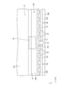
- FIG. Exploded perspective view showing schematic configuration of liquid crystal display device Sectional drawing of the cross section which cut
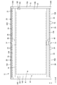
- a plan view of the backlight device viewed from the front side The top view which expanded the site
- Embodiment 2 the top view which expanded the site
- part which faces between adjacent LED boards among the edge of the light-incidence surface side of the light-projection surface of a light-guide plate, and its vicinity is shown.
- Embodiment 3 the photograph which shows the brightness
- the television receiver 1 includes a liquid crystal display device (an example of a display device) 10, front and back cabinets CA ⁇ b> 1 and CA ⁇ b> 2 that are accommodated so as to sandwich the liquid crystal display device 10, a power source 2, and a tuner 4. And a stand 6.
- a part of each drawing shows an X-axis, a Y-axis, and a Z-axis, and each axis direction is drawn in a common direction in each drawing.
- the X-axis direction coincides with the horizontal direction
- the Y-axis direction coincides with the vertical direction
- the Z-axis direction coincides with the thickness direction (front and back direction).
- the upper side of the figure coincides with the front side of the liquid crystal display device 10.
- the liquid crystal display device 10 has a horizontally long rectangular shape as a whole, and includes a liquid crystal panel (an example of a display panel) 11 and a backlight device (an example of an illumination device) 12 that is an external light source. It is integrally held by the formed bezel 13 or the like.
- the liquid crystal panel 11 is assembled in a posture in which a display surface 11C capable of displaying an image faces the front side.
- the liquid crystal panel 11 in the present embodiment is a high-definition panel having a large number of pixels, a so-called 4K2K panel, and has a large size of, for example, 32 types or more.
- the bezel 13 is made of a metal having excellent rigidity such as stainless steel. As shown in FIGS. 2 and 3, the bezel 13 is parallel to the liquid crystal panel 11 and has a substantially frame shape in plan view.
- the bezel frame-shaped portion 13A includes a bezel tubular portion 13B extending in a substantially short tubular shape from the outer peripheral end portion toward the back side.
- the bezel frame portion 13A extends along the edge of the display surface 11C of the liquid crystal panel 11.
- a buffer material 26A is disposed between the bezel frame-shaped portion 13A and the liquid crystal panel 11 (see FIG. 3), and the bezel frame-shaped portion 13A has the edge of the display surface 11C on the front side through the buffer material 26A.
- the liquid crystal panel 11 is held by pressing from the side.
- the bezel cylindrical portion 13 ⁇ / b> B covers a part of a frame 14 to be described later and constitutes a part of a side appearance of the liquid crystal display device 10.
- the liquid crystal panel 11 has a horizontally long rectangular shape in a plan view, and a predetermined interval is provided between the optical sheet group 16 and the optical sheet group 16 described later. Provided and stacked.
- the liquid crystal panel 11 is configured such that glass substrates 11A and 11B having excellent translucency are bonded together with a predetermined gap therebetween, and liquid crystal is sealed between the substrates 11A and 11B.
- the back side is the array substrate 11A
- the front side is the color filter substrate 11B. As shown in FIG.
- a display area A1 capable of displaying an image is arranged in the majority, and an area outside the display area A1 is a non-display area A2 where no image is displayed.
- a display area A1 capable of displaying an image is arranged on a large part of the display surface 11C, and an area outside the display area A1 forms a frame surrounding the display area A1 and the bezel of the bezel 13
- the non-display area A2 is covered with the frame-like portion 13A and no image is displayed (see FIGS. 3 and 5).
- a polarizing plate (not shown) is disposed outside both the substrates 11A and 11B.
- the array substrate 11A is provided with switching elements (for example, TFTs) connected to mutually orthogonal source lines and gate lines, pixel electrodes connected to the switching elements, and an alignment film.
- the array substrate 11A is provided with a large number of TFTs and pixel electrodes arranged side by side, and a large number of TFTs and pixel electrodes are arranged around the TFTs and pixel electrodes so as to surround a gate wiring and a source wiring in a lattice shape. It is installed.
- the gate wiring and the source wiring are connected to the gate electrode and the source electrode, respectively, and the pixel electrode is connected to the drain electrode of the TFT.
- the color filter substrate 11B is provided with a color filter in which colored portions such as R (red), G (green), and B (blue) are arranged in a predetermined arrangement, a counter electrode, and an alignment film. Yes.
- the array substrate 11A is slightly larger than the color filter substrate 11B so that its outer peripheral end protrudes outward from the outer peripheral end of the color filter substrate 11B over the entire periphery. Is formed.
- a plurality of gate side terminal portions (not shown) routed from the gate wirings described above are provided at both ends on the short side constituting the outer peripheral end of the array substrate 11A.
- a plurality of gate side flexible substrates 28 having flexibility (flexibility) are connected to each gate side terminal portion.
- the one on the long side (the upper right side in FIG. 2) has a source side terminal routed from the above-described source wiring.
- a plurality of parts (not shown) are provided.
- a plurality of source-side flexible substrates 30 having flexibility (flexibility) are connected to these source-side terminal portions.
- the gate side flexible substrate 28 and the source side flexible substrate 30 are made of synthetic resin having insulation and flexibility, respectively.
- a gate driver D1 for driving liquid crystal is mounted on the back surface of the gate side flexible substrate 28, and a source driver D2 is mounted on the back surface of the source side flexible substrate 30.
- Both drivers D1 and D2 have a protruding shape that protrudes inward from the mounting surface, and have a horizontally long shape.
- Both drivers D1 and D2 are composed of LSI chips having a drive circuit therein, and process input signals relating to images supplied from a control board (not shown) as a signal supply source to output output signals. The output signal is output to the liquid crystal panel 11.
- one end of the source side flexible substrate 30 is connected to the array substrate 11A, and the other end is bent and led to the back side of the bottom plate portion 15A of the chassis 15 described later. It is connected to the source substrate 32 arranged on the back side.
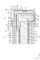
- the backlight device 12 is mainly composed of a frame (an example of a frame-like member) 14 that forms the front side appearance of the backlight device 12, and the back side appearance of the backlight device 12. Is accommodated in a space held between the chassis 15 and the chassis 15. Main components housed between the frame 14 and the chassis 15 include at least a light guide plate 18, a reflection sheet 21, and a plurality of LED units 20. The light guide plate 18 is held between the frame 14 and the chassis 15, and the optical sheet group 16 is laminated on the front side of the light guide plate 18. Each LED unit 20 is paired in a space between the frame 14 and the chassis 15 so as to sandwich the light guide plate 18 from both sides in the short side direction.
- the backlight device 12 according to the present embodiment is a so-called edge light type.
- the light guide plate 18 is made of a synthetic resin material (for example, acrylic resin such as PMMA or polycarbonate) having a refractive index sufficiently higher than that of air and substantially transparent (excellent translucency). As shown in FIG. 2, the light guide plate 18 has a horizontally long rectangular shape when viewed in a plane, like the liquid crystal panel 11 and the optical sheet group 16 described later, and the long side direction on the plate surface is the X-axis direction. The short side direction coincides with the Y-axis direction, and the thickness direction perpendicular to the plate surface coincides with the Z-axis direction.
- the light guide plate 18 is supported by a chassis 15 described later. Both end surfaces on the long side of the light guide plate 18 are light incident surfaces 18A on which light emitted from the LED units 20 is incident.
- the light guide plate 18 is in a posture in which the pair of light incident surfaces 18A are opposed to the respective LED units 20, and the light emitting surface 18B, which is the main plate surface (the plate surface on the front side), is directed to the optical sheet group 16 side.
- the opposite surface 18C which is the plate surface opposite to 18B (the plate surface on the back side), is arranged in a posture toward the reflection sheet 21 side described later.
- the light guide plate 18 introduces the light emitted from each LED unit 20 from each light incident surface 18A, rises toward the optical sheet group 16 side while propagating the light inside, and exits from the light exit surface 18B. It has a function to make it.
- a plurality of dot patterns (not shown) for light reflection are provided on the opposite surface 18C of the light guide plate 18.
- notches 18D that are recessed inwardly toward the inner side (center side of the light guide plate 18) are formed in the vicinity of the edge on the light incident surface 18A side on both end surfaces on the short side of the light guide plate 18. Is provided.
- Each notch 18D is provided so as to penetrate the light guide plate 18 in the thickness direction (Z-axis direction) so as to have a rectangular shape in plan view.
- the reflection sheet 21 is a rectangular sheet-like member, made of synthetic resin, and has a white surface with excellent light reflectivity.
- the reflection sheet 21 has a long side direction that coincides with the X-axis direction and a short side direction that coincides with the Y-axis direction, and is in contact with both in a state of being sandwiched between the light guide plate 18 and the chassis 15. is doing.
- the reflection sheet 21 can reflect light leaked from each LED unit 20 or the light guide plate 18 to the surface side of the reflection sheet 21.
- the optical sheet group 16 has a horizontally long rectangular shape when viewed in a plane, similar to the light guide plate 18 and the liquid crystal panel 11, and the size viewed in the plane is a light emitting surface of the light guide plate 18. It is supposed to be slightly smaller than 18B. As shown in FIG. 3, the optical sheet group is arranged so as to overlap the entire display area A ⁇ b> 1 of the liquid crystal panel 11, and its edge portion overlaps the non-display area A ⁇ b> 2 of the liquid crystal panel 11. The optical sheet group 16 is stacked on the light emitting surface 18 ⁇ / b> B of the light guide plate 18 and is disposed at a predetermined interval from the liquid crystal panel 11.
- the optical sheet group 16 is formed by laminating three optical sheets, a diffusion sheet 16A, a prism sheet 16B, and a reflective polarizing sheet 16C, in order from the light guide plate 18 side.
- the optical sheet group 16 is disposed so as to be interposed between the light guide plate 18 and the liquid crystal panel 11, thereby transmitting light emitted from the light guide plate 18 and giving a predetermined optical action to the transmitted light. The light is emitted to the liquid crystal panel 11.
- the chassis 15 constitutes the external appearance of the back side of the liquid crystal display device 10.
- the chassis 15 is made of a metal such as aluminum, and as shown in FIG. 2, the chassis 15 has a generally horizontally shallow shallow plate shape as a whole so as to cover the entire back side of the liquid crystal display device 10.
- the chassis 15 includes a bottom plate portion 15A that covers the back side of the liquid crystal panel 11, and side plate portions 15B that rise from the edges on both long sides of the bottom plate portion 15A to the front side. Further, both end portions on the long side of the bottom plate portion 15A are stepped portions 15A1 that protrude from the bottom plate portion 15A toward the back side of the liquid crystal display device 10 (see FIG. 3). As shown in FIG.
- the side plate portion 15B has a rising dimension (Z-axis direction dimension) substantially equal to the thickness dimension of the light guide plate 18 plus the projecting dimension of the stepped portion 15A1.
- the entire area of the back side of the LED unit 20 (the side opposite to the light emitting side of the LED 24) is covered.
- each positioning portion 15C has the same position in the short side direction (Y-axis direction) of the bottom plate portion 15A, and is perpendicular to the bottom plate portion 15A (Z-axis direction) so as to be the target with the light guide plate 18 in between.
- Each of the positioning portions 15C when viewed in a plan view shown in FIG. 5, fits in each of the cutouts 18D with almost no gap between each portion and the cutouts 18D provided on the light guide plate 18. ing. Thereby, the light guide plate 18 is positioned with respect to the bottom plate portion 15A.
- a sheet-like first heat radiation sheet HS1 having heat radiation properties is disposed between the bottom plate part 15A of the chassis 15 and the source substrate 32, as shown in FIG. 4, a sheet-like first heat radiation sheet HS1 having heat radiation properties is disposed between the bottom plate part 15A of the chassis 15 and the source substrate 32, as shown in FIG. 4, a sheet-like first heat radiation sheet HS1 having heat radiation properties is disposed between the bottom plate part 15A of the chassis 15 and the source substrate 32, as shown in FIG. 4, a sheet-like first heat radiation sheet HS1 having heat radiation properties is disposed between the bottom plate part 15A of the chassis 15 and the source substrate 32, as shown in FIG. 4, a sheet-like first heat radiation sheet HS1 having heat radiation properties is disposed between the bottom plate part 15A of the chassis 15 and the source substrate 32, as shown in FIG. 4, a sheet-like first heat radiation sheet HS1 having heat radiation properties is disposed between the bottom plate part 15A of the chassis 15 and the source substrate 32, as shown in FIG. 4, a
- the frame 14 is formed in a horizontally long frame shape like the bezel 13 and is made of synthetic resin.
- the frame 14 is parallel to the liquid crystal panel 11 and has a substantially frame shape in a plan view, and a frame extending in a substantially short tube shape from the outer peripheral end of the frame frame portion 14A toward the front and back sides. It consists of the cylindrical part 14B.
- 14 A of frame frame-shaped parts are extended along the edge of the light-projection surface 18B of the light-guide plate 18, The one part presses the outermost edge part among the edges of the light-projection surface 18B from a front side, and is a chassis.
- the light guide plate 18 is sandwiched between the 15 bottom plate portions 15A.
- the frame frame-like portion 14A is provided with a cover portion 14A1 that covers the edge of the light emitting surface 18B and the edge of the optical sheet group 16 from the front side by protruding inward from the portion sandwiching the light guide plate 18. (See FIG. 4).
- a buffer material 26B is disposed between the frame frame-shaped portion 14A and the liquid crystal panel 11, and the frame frame-shaped portion 14A supports the edge of the liquid crystal panel 11 from the back side via the buffer material 26B. ing.
- the length of the part extending from the outer peripheral end of the frame frame part 14A to the back side of the frame cylindrical part 14B is longer than the length of the part extending to the front side.
- the portion extending to the back side is assigned to most of both side plate portions 15B of the chassis 15 and constitutes a part of the appearance of the side surface of the liquid crystal display device 10.
- a portion of the frame cylindrical portion 14B that is addressed to one side plate portion 15B is provided with a concave driver accommodating portion 14B1 that opens to the outside and accommodates the source driver D1 (see FIG. 4). ).
- the source driver D2 is accommodated in the driver accommodating portion 14B1 while maintaining a non-contact state with respect to the driver accommodating portion 14B1. Thereby, most of the heat generated in the source driver D2 due to the driving of the source driver D2 is propagated to the mounting portion of the source driver D2 on the source-side flexible substrate 30.
- each LED unit 20 includes an LED substrate 25 and a plurality of LEDs 24 mounted on the LED substrate 25.
- the LED 24 constituting each LED unit 20 is configured such that an LED chip (not shown) is sealed with a resin material on a substrate portion fixed to the LED substrate 25.
- the LED chip mounted on the substrate unit has one main emission wavelength, and specifically, one that emits blue light in a single color is used.
- the resin material for sealing the LED chip is dispersed and blended with a phosphor that emits a predetermined color when excited by blue light emitted from the LED chip, and generally emits white light as a whole. Is done.
- a yellow phosphor that emits yellow light for example, a green phosphor that emits green light, and a red phosphor that emits red light are used in appropriate combination, or any one of them is used. It can be used alone.
- the LED 24 is a so-called top surface light emitting type in which a surface opposite to a surface on which the LED substrate 25 is mounted is a main light emitting surface.
- the LED substrate 25 that constitutes the LED unit 20 is made of aluminum having excellent heat dissipation, and as shown in FIGS. 2 and 5, is elongated and extends along the long side direction (X-axis direction) of the light guide plate 18. It has a plate shape and is vertically supported by the step portion 15A1 of the bottom plate portion 15A of the chassis 15. Specifically, the LED substrate 25 is arranged with its plate surface parallel to the X-axis direction and Z-axis direction, that is, the posture parallel to the light incident surface 18A of the light guide plate 18.
- Each LED substrate 25 has a length in the long side direction (X-axis direction) that is about half the size in the long side direction of the light guide plate 20, and has a predetermined length along the light incident surface 18 ⁇ / b> A of the light guide plate 18. Two are arranged side by side at intervals. Each LED board 25 has a short side direction dimension substantially equal to the thickness dimension of the light guide plate 18 plus the projecting dimension of the step portion 15A1 (see FIG. 3).
- a plurality of LEDs 24 are surface-mounted on a plate surface inside the LED substrate 25, that is, a plate surface facing the light guide plate 18, and this surface is a mounting surface 25A.
- Each LED 24 is disposed by being soldered directly to the mounting surface 25A of the LED substrate 25 with its light emitting surface 24A facing the light incident surface 18A of the light guide plate 18.
- the LEDs 24 are arranged in a line (linearly) at a substantially equal pitch along the length direction (X-axis direction) on the mounting surface 25 ⁇ / b> A of the LED substrate 25.
- a wiring pattern (not shown) that is made of a metal film (such as copper stay) and supplies driving power to each LED 24 is formed.
- seat HS2 which has heat dissipation is distribute
- the second heat radiating sheet HS2 is in contact with both between the LED board 25 and the side plate portion 15B, whereby a part of the heat propagated to the LED board 25 passes through the second heat radiating sheet HS2. It is configured to be effectively propagated to the side plate portion 15B.
- a light reflecting member 40 having light reflectivity is arranged on a part of the back side of the cover portion 14 ⁇ / b> A ⁇ b> 1 in the frame frame-like portion 14 ⁇ / b> A of the frame 14. ing.
- the light reflecting member 40 has a sheet shape, and one surface has adhesiveness so that the light reflecting member 40 is affixed to the covering portion 14A1.
- the light reflecting member 40 is a portion facing the S ⁇ b> 1 between the LED substrates 25 adjacent to each other on the light incident surface 18 ⁇ / b> A side edge of the light emitting surface 18 ⁇ / b> B of the light guide plate 18.
- each light reflecting member 40 is arranged in the form facing each other. As shown in FIG. 5, in the plan view of the backlight device 12, most of each light reflecting member 40 faces the light emitting surface 18 ⁇ / b> B of the light guide plate 18, and a part of the light reflecting member 40 overlaps with the optical sheet group 16. ing. Further, as shown in FIG. 5, each light reflecting member 40 is arranged in the vicinity of the boundary portion with the display area A ⁇ b> 1 in the non-display area A ⁇ b> 2 of the liquid crystal panel 11.
- the interval between the adjacent LEDs 24 at S ⁇ b> 1 between the two adjacent LED substrates 25 is mounted on the mounting surface 25 ⁇ / b> A of the LED substrate 25. It becomes larger than the interval between the LEDs 24.
- the light reflecting member 40 described above is not provided, when the edge of the light emitting surface 18B of the light guide plate 18 on the light incident surface 18A side is viewed, the adjacent LED substrate 25 among the edges.
- the part that faces S1 during the period may be displayed relatively darker than other parts, and a dark part may occur in the part that faces. And when this dark part arises to a part of display area A1 of the liquid crystal panel 11, the brightness nonuniformity resulting from the said dark part arises in the image displayed on the display surface 11C.
- the light that has reached the light reflecting member 40 is exposed to the portion facing the S1 between the adjacent LED substrates 25 on the light incident surface 18A side edge of the light emitting surface 18B of the light guide plate 18 by the light reflecting member 40. Reflected.
- the reflected light reaches the dark part generated in the vicinity and the vicinity thereof, and the dark part generated in the display area A1 in addition to the dark part generated in the non-display area A2 can be eliminated.
- the optical sheet interferes with the light reflecting member when the optical sheet group disposed on the light emitting surface undergoes thermal expansion or the like. There is a risk of doing.
- the light reflecting member 40 is attached to a part of the frame 14, that is, the covering portion 14A1 of the frame 14. For this reason, it can suppress that the light reflection member 40 interferes with another member resulting from the thermal expansion etc. of another member.
- ⁇ Modification 1 of Embodiment 1> A first modification of the first embodiment will be described with reference to FIG.
- the number of LED units 120 provided in the backlight device 112 and the number of light reflecting members 140 are different from those in the first embodiment. Other configurations are the same as those in the first embodiment.
- the backlight device 112 according to this modification as shown in FIG. 7, six LED units 20 are accommodated in the chassis 15. That is, the length dimension of the LED substrate 125 constituting each LED unit 120 is shorter than that of the first embodiment, and each LED substrate 125 has a predetermined interval along the light incident surface 18A of the light guide plate 18. Three are arranged side by side while being vacant. Further, four light reflecting members 140 are accommodated in the chassis 15.
- each light reflecting member 140 is arranged in a form facing the portion facing the S ⁇ b> 2 between the adjacent LED substrates 125 on the light incident surface 18 ⁇ / b> A side edge of the light emitting surface 18 ⁇ / b> B of the light guide plate 18. .
- each light out of the light emitted from the light emitting surface 18B of the light guide plate 18 is used.
- the light reaching the reflecting member 140 is reflected by the light reflecting member 140 to a portion facing the S2 between the adjacent LED substrates 125 in the edge on the light incident surface 18A side of the light emitting surface 18B of the light guide plate 18. .
- the reflected light reaches the dark part generated in the vicinity and the vicinity thereof, and the dark part generated in the display area A1 in addition to the dark part generated in the non-display area A2 can be eliminated. It can suppress that the brightness nonuniformity resulting from the said dark part arises in the image displayed on a surface.
- ⁇ Modification 2 of Embodiment 1> A second modification of the first embodiment will be described.
- the cover portion of the frame in which the light reflecting member 40 is disposed in Embodiment 1 in the frame is painted white so that the entire cover portion has light reflectivity. It is a light reflecting member. For this reason, the sheet-like light reflection member is not arranged in the covering part.
- the cover portion since the cover portion is painted in white as a light reflecting member in this way, the thickness of the light reflecting member becomes equal to the thickness of the coating. The thickness of the light reflecting member can be reduced as compared with the case where the reflecting member is provided. As a result, the backlight device can be thinned.
- the arrangement of the light reflecting members 240 is different from that of the first embodiment. Since other configurations are the same as those of the first embodiment, description thereof is omitted.
- the light reflecting member 240 is attached to the light emitting surface 18 ⁇ / b> B of the light guide plate 18. Specifically, as shown in FIG. 9, the light reflecting member 240 is attached to a portion of the light emitting surface 18 ⁇ / b> B of the light guide plate 18 on the light incident surface 18 ⁇ / b> A side facing the S ⁇ b> 3 between the adjacent LED substrates 25. Are arranged.
- the light reflecting member since the light reflecting member is arranged as described above, light that is about to be emitted from a portion of the light emitting surface 18B of the light guide plate 18 to which each light reflecting member 240 is attached. However, the light reflecting member 240 reflects the portion of the light guide plate 18 facing the S3 between the adjacent LED substrates 125 and the vicinity thereof. Thereby, the reflected light reaches the part facing the S3 between the adjacent LED substrates 25 and the dark part generated in the vicinity of the edge on the light incident surface 18A side of the light emitting surface 18B of the light guide plate 18.
- FIG. 10 Illustrate the photo.
- A3 the brightness difference is hardly seen compared with the other part of the light-projection surface 18B of the light-guide plate 18.
- the light reflecting member 240 is disposed, so that the dark portion generated in the display region A1 in addition to the dark portion generated in the non-display region A2 of the liquid crystal panel 11 is eliminated.
- the plurality of circular patterns visible on the light guide plate 18 are dot patterns for light reflection provided on the opposite surface 18 ⁇ / b> C of the light guide plate 18.
- Embodiment 3 will be described with reference to FIGS.
- a protruding portion (an example of a light scattering member) 316D that protrudes in a convex shape toward the LED substrate 25 side is provided on a part of the side edge.
- the protruding portion 316D is provided so as to face a portion facing the S4 between the adjacent LED substrates 25 on the light incident surface 18A side edge of the light emitting surface 18B of the light guide plate 18. Has scattering properties. Further, as shown in FIG. 12, the protrusion 316D is located in the vicinity of the boundary with the display area A1 in the non-display area A2 of the liquid crystal panel 311. In addition, about the other structure of the liquid crystal display device 310 which concerns on this embodiment, since it is the same as that of Embodiment 1, description is abbreviate
- the protruding portion 316D having light scattering properties is provided in the above-described arrangement manner, so that the protruding portion of the light emitted from the light emitting surface 18B of the light guide plate 18 is provided.
- the light that has reached 316D is scattered by the protrusion 316D to a portion facing the S4 between the adjacent LED substrates 25 on the light incident surface 18A side edge of the light exit surface 18B of the light guide plate 18.
- the protrusion 316D is scattered in the facing part and its vicinity, and the brightness of the dark part generated in the facing part and its vicinity is increased, and the difference in brightness between the dark part and the other part is reduced.
- FIG. 13 shows the luminance in the vicinity of the portion facing the S4 between the adjacent LED substrates 25 on the light incident surface 18A side edge of the light emitting surface 18B of the light guide plate 18 in this embodiment. Illustrate the photo.
- A4 compared with the other part of the light-projection surface 18B of the light-guide plate 18, a brightness difference is hardly seen.
- the projection 316D is provided on the prism sheet 316B of the optical sheet group 316, so that the dark part generated in the display area A1 in addition to the dark part generated in the non-display area A2 of the liquid crystal panel 11 is eliminated. .
- the protrusions are provided so as to overlap all the optical sheets constituting the optical sheet group 416 in this way, compared with that of the fourth embodiment.
- the effect of scattering light that reaches the protrusion 416D is enhanced.
- light is further scattered by the protrusions 416D at the portion facing the adjacent LED substrate 25 and the vicinity thereof on the light incident surface 18A side edge of the light emitting surface 18B of the light guide plate 18.
- the brightness of the dark part generated in the region and the vicinity thereof is further increased. As a result, it is possible to effectively suppress the occurrence of luminance unevenness due to the dark portion in the image displayed on the display surface of the liquid crystal panel 11.
- ⁇ Modification 2 of Embodiment 3> A first modification of the third embodiment will be described with reference to FIG.
- the projection 416D is provided only on the prism sheet 416B among the optical sheets constituting the optical sheet group 416 as in the fourth embodiment.
- a light reflecting member 540 having the same configuration as that of the light reflecting member 40 described in the first embodiment is attached to the back side of the protruding portion 416D (the side facing the light emitting surface 18B of the light guide plate 18). Yes.
- the same effect as that of the backlight device 12 of the first embodiment can be obtained by adopting such a configuration. That is, the light that has reached the light reflecting member 540 out of the light emitted from the light emitting surface 18B of the light guide plate 18 is caused to end by the light reflecting member 540 on the light incident surface 18A side of the light emitting surface 18B of the light guide plate 18. It is reflected by the site
- each modification of the first embodiment, and the second embodiment as an example of the light reflecting member, a sheet-like member and a part of the frame that are painted white are exemplified.
- the reflection member is not limited as long as it has light reflectivity.
- the configuration in which the protruding portion protruding in a convex shape is provided in a part of the optical sheet group is illustrated, but the shape of the protruding portion is not limited. .
- the protruding portion may be provided in a shape protruding in a semicircular shape, or may be provided in a shape protruding in a triangular shape.
- the protrusions provided in a part of the optical sheet group are exemplified as an example of the light scattering member.
- the configuration of the light scattering member is not limited.
- the backlight device may separately include a light scattering member such as a sheet.
- each end face on both long sides of each end face of the light guide plate is a light incident face
- the configuration in which the LED substrate is arranged to face each light incident face is exemplified.
- all the end faces of the light guide plate may be light incident surfaces, and the LED substrate may be arranged to face each light incident surface.
- the light reflecting member or the light scattering member in a form facing the portion facing between the adjacent LED substrates among the edges on the light incident surface side of the light emitting surface of the light guide plate, It can suppress that the brightness nonuniformity resulting from the said dark part arises in the image displayed on the display surface of a liquid crystal panel.
- a high-definition liquid crystal panel has been exemplified.
- the present invention can also be applied to a display panel that is not high-definition.
- the present invention it is possible to suppress the occurrence of luminance unevenness due to the dark portion in the image displayed on the display surface of the liquid crystal panel. it can.
- a television receiving device of a type including a cabinet is illustrated, but the present invention is applicable to a type not including a cabinet.
- a television receiver including a high-definition liquid crystal panel has been exemplified.
- the present invention can be applied to display devices other than the television receiver.
Abstract
A lighting device (12) is provided with: light sources (24); a light-guiding plate (18) formed such that at least one end surface thereof is configured as a light entry surface (18A) through which light from the light sources (24) enters, and another plate surface is configured as a light exit surface (18B) through which light that has entered from the light entry surface (18A) is allowed to exit; a plurality of light source substrates (25) configured such that one plate surface is configured as a mounting surface (25A) on which a plurality of light sources (24) are mounted, the plurality of light source substrates being disposed along the light entry surface (18A) such that the mounting surfaces face toward the light entry surface (18A); and a light-reflecting member (40) having light-reflective properties, the light-reflecting member (40) being disposed so as to face toward a location on the light-entry-surface (18A)-side outer edge of the light exit surface (18B) that faces toward a space (S1) between adjacent light source substrates (25).
Description
本発明は、照明装置、表示装置、及びテレビ受信装置に関する。
The present invention relates to a lighting device, a display device, and a television receiver.
例えば、液晶テレビなどの液晶表示装置は、その表示パネルである液晶パネルが自発光しないため、別途に照明装置としてバックライト装置を必要としている。バックライト装置はその機構によって直下型とエッジライト型とに大別されており、液晶表示装置の一層の薄型化を実現するには、エッジライト型のバックライト装置を用いるのが好ましいものとされている。
For example, a liquid crystal display device such as a liquid crystal television requires a backlight device as a separate illumination device because the liquid crystal panel that is the display panel does not emit light. Backlight devices are roughly classified into direct type and edge light type according to the mechanism, and it is preferable to use an edge light type backlight device in order to realize further thinning of the liquid crystal display device. ing.
エッジライト型のバックライト装置では、少なくとも一つの端面に光入射面が設けられるとともに一方の板面が光出射面とされた導光板、実装面上にLED(Light Emitting Diode)等の光源が複数実装され、実装面が導光板の光出射面と対向する形で配される光源基板、等が筐体内に収容される。この種のバックライト装置では、導光板の光出射面から出射される光に輝度ムラが生じることがあり、このような輝度ムラを抑制することが要求される。例えば下記特許文献1には、導光板に設けた位置決め突起部の近傍に発生する輝度ムラの防止を図った面状照明装置が開示されている。
In an edge light type backlight device, a light guide plate having a light incident surface provided on at least one end surface and a light emitting surface on one plate surface, and a plurality of light sources such as LEDs (Light Emitting Diodes) on the mounting surface A light source substrate, etc., which is mounted and disposed so that the mounting surface faces the light emitting surface of the light guide plate, is accommodated in the housing. In this type of backlight device, brightness unevenness may occur in the light emitted from the light exit surface of the light guide plate, and it is required to suppress such brightness unevenness. For example, Patent Document 1 below discloses a planar illumination device that prevents luminance unevenness that occurs in the vicinity of a positioning protrusion provided on a light guide plate.
(発明が解決しようとする課題)
ところで、近年需要が高まっている高精細の液晶パネルや高色再現性の液晶パネルにおいては、当該液晶パネルに光を供給するバックライト装置について導光板の光出射面から出射される光に高い輝度が要求され、多数の光源が必要とされる。そこで、バックライト装置の筐体内に多数の光源を配置するため、導光板の光入射面に沿って光源基板が複数並んで配されることがある。 (Problems to be solved by the invention)
By the way, in a high-definition liquid crystal panel and a liquid crystal panel with high color reproducibility, which have been increasing in demand in recent years, high brightness is obtained for light emitted from the light exit surface of the light guide plate for a backlight device that supplies light to the liquid crystal panel. Is required, and a large number of light sources are required. Therefore, in order to arrange a large number of light sources in the casing of the backlight device, a plurality of light source substrates may be arranged along the light incident surface of the light guide plate.
このように導光板の光入射面に沿って光源基板が複数並んで配されると、隣り合う光源基板の間で隣り合う光源の間隔が、光源基板の実装面上に実装された各光源の間隔に比べて大きくなる。このため、導光板の光出射面の光入射面側の端縁を視たときに、当該端縁のうち隣り合う光源基板の間に臨む部位が他の部位と比べて相対的に暗く表示されることがある。即ち、上記臨む部位に暗部が生じることがある。その結果、導光板の光出射面から出射される光に上記暗部に起因する輝度ムラが生じることがある。
As described above, when a plurality of light source substrates are arranged along the light incident surface of the light guide plate, the interval between the adjacent light sources between the adjacent light source substrates is the distance between each light source mounted on the mounting surface of the light source substrate. Larger than the interval. For this reason, when the edge on the light incident surface side of the light emitting surface of the light guide plate is viewed, a portion of the edge facing the adjacent light source substrate is displayed relatively darker than other portions. Sometimes. That is, a dark part may occur at the facing part. As a result, unevenness in brightness due to the dark portion may occur in the light emitted from the light exit surface of the light guide plate.
本明細書で開示される技術は、上記の課題に鑑みて創作されたものであって、輝度ムラを抑制することを目的とする。
The technology disclosed in this specification has been created in view of the above problems, and aims to suppress luminance unevenness.
(課題を解決するための手段)
本明細書で開示される技術は、光源と、少なくとも一つの端面が前記光源からの光が入射される光入射面とされ、一方の板面が前記光入射面から入射された光が出射される光出射面とされた導光板と、一方の板面が複数の前記光源が実装された実装面とされ、該実装面が前記光入射面と対向する形で前記光入射面に沿って並んで配された複数の光源基板と、光反射性を有し、前記光出射面の前記光入射面側の端縁のうち隣り合う前記光源基板の間に臨む部位と対向する形で配される光反射部材と、を備える照明装置に関する。 (Means for solving the problem)
In the technology disclosed in this specification, a light source and at least one end surface are a light incident surface on which light from the light source is incident, and one plate surface emits light incident from the light incident surface. A light guide plate having a light emitting surface and a mounting surface on which one of the light sources is mounted, and the mounting surface is arranged along the light incident surface so as to face the light incident surface. And a plurality of light source substrates arranged in a manner of being opposed to a portion that has light reflectivity and faces between the adjacent light source substrates among the edges of the light emitting surface on the light incident surface side. And a light reflecting member.
上記の照明装置のように導光板の光入射面に沿って光源基板が複数並んで配される構成では、隣り合う光源の間隔が光源基板の実装面上に実装された各光源の間隔に比べて大きくなるため、導光板の光出射面の光入射面側の端縁のうち隣り合う光源基板の間に臨む部位に暗部が生じ、光出射面から出射される光に輝度ムラが生じることがある。これに対し上記の照明装置では、導光板の光出射面から出射された光のうち光反射部材に到達した光が、当該光反射部材によって、導光板の光出射面の光入射面側の端縁のうち隣り合う光源基板の間に臨む部位に反射される。これにより、上記臨む部位及びその近傍に生じる暗部に上記反射された光が到達し、当該暗部をなくすことができる。このため、導光板の光出射面から出射される光に上記暗部に起因する輝度ムラが生じることを抑制することができる。
In the configuration in which a plurality of light source substrates are arranged along the light incident surface of the light guide plate as in the lighting device described above, the interval between adjacent light sources is larger than the interval between the light sources mounted on the mounting surface of the light source substrate. Therefore, a dark part occurs in a portion of the light emitting surface of the light guide surface on the light incident surface side that faces between adjacent light source substrates, and unevenness in luminance occurs in the light emitted from the light emitting surface. is there. On the other hand, in the illumination device described above, the light that has reached the light reflecting member out of the light emitted from the light emitting surface of the light guide plate is caused by the light reflecting member to end the light incident surface side of the light emitting surface of the light guide plate. It is reflected by the part which faces between adjacent light source substrates among edges. Thereby, the reflected light reaches the dark part generated in the facing part and the vicinity thereof, and the dark part can be eliminated. For this reason, it can suppress that the brightness nonuniformity resulting from the said dark part arises in the light radiate | emitted from the light-projection surface of a light-guide plate.
上記の照明装置において、前記光出射面の端縁を覆う覆い部を有する枠状部材を備え、前記光反射部材が前記覆い部の一部に貼り付けられて配されていてもよい。
The illumination device may include a frame-shaped member having a cover portion that covers an edge of the light emitting surface, and the light reflecting member may be attached to a part of the cover portion.
例えば光反射部材が導光板の光出射面上に配されていると、光出射面上に配された光学シート等が熱膨張等にした場合、当該光学シートが光反射部材と干渉する虞がある。上記の構成では、光反射部材が枠状部材の覆い部に貼り付けられることで、このような光反射部材と他の部材との干渉を抑制することができる。
For example, when the light reflecting member is disposed on the light emitting surface of the light guide plate, when the optical sheet or the like disposed on the light emitting surface undergoes thermal expansion, the optical sheet may interfere with the light reflecting member. is there. In said structure, interference with such a light reflection member and another member can be suppressed because a light reflection member is affixed on the cover part of a frame-shaped member.
上記の照明装置において、前記光出射面の端縁を覆う覆い部を有する枠状部材を備え、前記光反射部材は、前記覆い部の一部が白色に塗装されることでなってもよい。
The illumination device may include a frame-like member having a cover portion that covers an edge of the light emitting surface, and the light reflecting member may be formed by painting a part of the cover portion in white.
この構成では、光反射部材の厚みが塗装の厚みと等しくなるため、例えば光反射部材がシート状とされている場合と比べて光反射部材の厚みを薄くすることができる。このため、照明装置の薄型化を図ることができる。
In this configuration, since the thickness of the light reflecting member becomes equal to the thickness of the coating, for example, the thickness of the light reflecting member can be reduced as compared with the case where the light reflecting member is formed into a sheet shape. For this reason, thickness reduction of an illuminating device can be achieved.
上記の照明装置において、前記光反射部材が、前記光出射面の前記光入射面側の端縁の一部に貼り付けられて配されていてもよい。
In the illuminating device, the light reflecting member may be disposed by being attached to a part of an edge of the light emitting surface on the light incident surface side.
この構成によると、光反射部材についての具体的な配置態様を提供することができる。
According to this configuration, a specific arrangement mode for the light reflecting member can be provided.
上記の照明装置において、前記光出射面上に積層された複数の光学シートからなる光学シート群を備え、前記複数の光学シートのうち上層側に位置する光学シートの前記光入射面側の端縁に、前記光源基板側に突出する突出部が設けられ、前記光反射部材が前記突出部に貼り付けられて配されていてもよい。
In the illuminating device described above, an optical sheet group composed of a plurality of optical sheets stacked on the light emitting surface is provided, and an edge on the light incident surface side of the optical sheet located on the upper layer side of the plurality of optical sheets In addition, a protrusion that protrudes toward the light source substrate may be provided, and the light reflecting member may be attached to the protrusion.
例えば光反射部材が導光板の光出射面上に配されていると、光出射面上に配された光学シート等が熱膨張等にした場合、当該光学シートが光反射部材と干渉する虞がある。上記の構成では、光反射部材が光学シートの突出部に貼り付けられることで、このような光反射部材と他の部材との干渉を抑制することができる。
For example, when the light reflecting member is disposed on the light emitting surface of the light guide plate, when the optical sheet or the like disposed on the light emitting surface undergoes thermal expansion, the optical sheet may interfere with the light reflecting member. is there. In said structure, interference with such a light reflection member and another member can be suppressed because a light reflection member is affixed on the protrusion part of an optical sheet.
本明細書で開示される他の技術は、光源と、少なくとも一つの端面が前記光源からの光が入射される光入射面とされ、一方の板面が前記光入射面から入射された光が出射される光出射面とされた導光板と、一方の板面が複数の前記光源が実装された実装面とされ、該実装面が前記光入射面と対向する形で前記光入射面に沿って並んで配された複数の光源基板と、光散乱性を有し、前記光出射面の前記光入射面側の端縁のうち隣り合う前記光源基板の間に臨む部位と対向する形で配される光散乱部材と、を備える照明装置に関する。
In another technique disclosed in the present specification, a light source and at least one end surface is a light incident surface on which light from the light source is incident, and one plate surface receives light incident from the light incident surface. A light guide plate that is an emitted light exit surface, and one plate surface is a mounting surface on which a plurality of the light sources are mounted, and the mounting surface faces the light incident surface along the light incident surface. A plurality of light source substrates arranged side by side, and having a light scattering property, arranged so as to face a portion facing the adjacent light source substrate among the edges on the light incident surface side of the light emitting surface. And a light scattering member.
上記の照明装置では、導光板の光出射面から出射された光のうち光散乱部材に到達した光が、当該光散乱部材によって、導光板の光出射面の光入射面側の端縁のうち隣り合う光源基板の間に臨む部位に散乱される。これにより、上記臨む部位及びその近傍に生じる暗部の輝度が高められ、当該暗部と他の部位との間の輝度の差が低減される。このため、導光板の光出射面から出射される光に上記暗部に起因する輝度ムラが生じることを抑制することができる。
In the illuminating device described above, the light that has reached the light scattering member among the light emitted from the light exit surface of the light guide plate is out of the edge on the light incident surface side of the light exit surface of the light guide plate by the light scattering member. Scattered to a portion facing between adjacent light source substrates. Thereby, the brightness | luminance of the dark part which arises in the said location and its vicinity is raised, and the difference of the brightness | luminance between the said dark part and another site | part is reduced. For this reason, it can suppress that the brightness nonuniformity resulting from the said dark part arises in the light radiate | emitted from the light-projection surface of a light-guide plate.
上記の照明装置において、前記光出射面上に積層されるとともに該光出射面から出射される光に光学機能を付与する複数の光学シートからなる光学部材を備え、前記複数の光学シートのうち少なくとも一つの光学シートの前記光入射面側の端縁に、前記光源基板側に突出する突出部が設けられ、前記突出部が前記光散乱部材とされてもよい。
The illumination device includes an optical member including a plurality of optical sheets stacked on the light emission surface and imparting an optical function to light emitted from the light emission surface, and includes at least one of the plurality of optical sheets. A protrusion that protrudes toward the light source substrate may be provided at an edge of the light incident surface of one optical sheet, and the protrusion may be the light scattering member.
上記の構成では、光学シートの一部が光散乱部材とされるため、光散乱部材を別途配さなくともよく、部材コストの削減を図ることができる。
In the above configuration, since a part of the optical sheet is a light scattering member, it is not necessary to separately provide the light scattering member, and the member cost can be reduced.
上記の照明装置において、前記光源基板が金属製とされていてもよい。
In the above illumination device, the light source substrate may be made of metal.
金属製の光源基板は樹脂製のものと比べて放熱性に優れる一方、その延在方向の長さ寸法が一般的に樹脂製のものと比べて短い。このため、大型の照明装置では、導光板の光入射面に沿って多数の光源基板を並べて配する必要がある。この点、上記の構成では、多数の光源基板が並べて配された場合であっても、導光板の端縁のうち上記隣り合う光源基板の間に臨む部位にそれぞれ生じる上記暗部に起因して上記輝度ムラが生じることを抑制することができる。このため、輝度ムラが生じることを抑制しながら、大型の照明装置を実現するとともに放熱性を高めることができる。
The metal light source substrate is excellent in heat dissipation compared with the resin one, but its length in the extending direction is generally shorter than that of the resin one. For this reason, in a large illuminating device, it is necessary to arrange many light source substrates along with the light-incidence surface of a light-guide plate. In this regard, in the above configuration, even when a large number of light source substrates are arranged side by side, the above described dark portions are generated due to the dark portions respectively generated in the portions facing the adjacent light source substrates among the edges of the light guide plate. The occurrence of uneven brightness can be suppressed. For this reason, it is possible to realize a large illuminating device and enhance heat dissipation while suppressing the occurrence of luminance unevenness.
本明細書で開示される技術では、上記の照明装置と、当該照明装置から供給される光を利用して画像を表示する表示パネルと、を備える表示装置も新規で有用である。また、上記の表示装置を備えるテレビ受信装置も新規で有用である。
In the technology disclosed in this specification, a display device including the above-described illumination device and a display panel that displays an image using light supplied from the illumination device is also new and useful. A television receiver provided with the above display device is also new and useful.
(発明の効果)
本明細書で開示される技術によれば、エッジライト型のバックライト装置において、導光板から出射される光に生じる輝度ムラを抑制することができる。 (The invention's effect)
According to the technology disclosed in the present specification, luminance unevenness generated in light emitted from the light guide plate can be suppressed in the edge light type backlight device.
本明細書で開示される技術によれば、エッジライト型のバックライト装置において、導光板から出射される光に生じる輝度ムラを抑制することができる。 (The invention's effect)
According to the technology disclosed in the present specification, luminance unevenness generated in light emitted from the light guide plate can be suppressed in the edge light type backlight device.
<実施形態1>
図面を参照して実施形態1を説明する。本実施形態では、テレビ受信装置1について例示する。テレビ受信装置1は、図1に示すように、液晶表示装置(表示装置の一例)10と、当該液晶表示装置10を挟むようにして収容する表裏両キャビネットCA1,CA2と、電源2と、チューナー4と、スタンド6と、を備えている。なお、各図面の一部にはX軸、Y軸およびZ軸を示しており、各軸方向が各図面で共通した方向となるように描かれている。このうちX軸方向は水平方向と一致し、Y軸方向は鉛直方向と一致し、Z軸方向は厚み方向(表裏方向)と一致している。各斜視図及び各断面図では、図の上側が液晶表示装置10の表側と一致する。 <Embodiment 1>
Embodiment 1 will be described with reference to the drawings. In this embodiment, the television receiver 1 is illustrated. As shown in FIG. 1, the television receiver 1 includes a liquid crystal display device (an example of a display device) 10, front and back cabinets CA <b> 1 and CA <b> 2 that are accommodated so as to sandwich the liquid crystal display device 10, a power source 2, and a tuner 4. And a stand 6. A part of each drawing shows an X-axis, a Y-axis, and a Z-axis, and each axis direction is drawn in a common direction in each drawing. Among these, the X-axis direction coincides with the horizontal direction, the Y-axis direction coincides with the vertical direction, and the Z-axis direction coincides with the thickness direction (front and back direction). In each perspective view and each sectional view, the upper side of the figure coincides with the front side of the liquid crystal display device 10.
図面を参照して実施形態1を説明する。本実施形態では、テレビ受信装置1について例示する。テレビ受信装置1は、図1に示すように、液晶表示装置(表示装置の一例)10と、当該液晶表示装置10を挟むようにして収容する表裏両キャビネットCA1,CA2と、電源2と、チューナー4と、スタンド6と、を備えている。なお、各図面の一部にはX軸、Y軸およびZ軸を示しており、各軸方向が各図面で共通した方向となるように描かれている。このうちX軸方向は水平方向と一致し、Y軸方向は鉛直方向と一致し、Z軸方向は厚み方向(表裏方向)と一致している。各斜視図及び各断面図では、図の上側が液晶表示装置10の表側と一致する。 <
液晶表示装置10は、全体として横長の方形をなしており、液晶パネル(表示パネルの一例)11と、外部光源であるバックライト装置(照明装置の一例)12とを備え、これらが枠状をなすベゼル13などにより一体的に保持されるようになっている。液晶表示装置10において、液晶パネル11は、画像を表示可能な表示面11Cが表側を向いた姿勢で組み付けられている。なお、本実施形態における液晶パネル11は、画素数が多い高精細のパネル、いわゆる4K2Kパネルとされ、そのサイズが例えば32型以上とされた大型のものとなっている。
The liquid crystal display device 10 has a horizontally long rectangular shape as a whole, and includes a liquid crystal panel (an example of a display panel) 11 and a backlight device (an example of an illumination device) 12 that is an external light source. It is integrally held by the formed bezel 13 or the like. In the liquid crystal display device 10, the liquid crystal panel 11 is assembled in a posture in which a display surface 11C capable of displaying an image faces the front side. The liquid crystal panel 11 in the present embodiment is a high-definition panel having a large number of pixels, a so-called 4K2K panel, and has a large size of, for example, 32 types or more.
ベゼル13は、ステンレスなどの剛性に優れた金属製とされており、図2及び図3に示すように、液晶パネル11に並行するとともに平面視において略枠状をなすベゼル枠状部13Aと、当該ベゼル枠状部13Aの外周端部から裏側に向けて略短筒状に延びるベゼル筒状部13Bとからなる。ベゼル枠状部13Aは、液晶パネル11の表示面11Cの端縁に沿って延在している。ベゼル枠状部13Aと液晶パネル11との間には緩衝材26Aが配されており(図3参照)、ベゼル枠状部13Aは、この緩衝材26Aを介して表示面11Cの端縁を表側から押さえることで液晶パネル11を保持している。ベゼル筒状部13Bは、後述するフレーム14の一部を覆うとともに液晶表示装置10における側面の外観の一部を構成している。
The bezel 13 is made of a metal having excellent rigidity such as stainless steel. As shown in FIGS. 2 and 3, the bezel 13 is parallel to the liquid crystal panel 11 and has a substantially frame shape in plan view. The bezel frame-shaped portion 13A includes a bezel tubular portion 13B extending in a substantially short tubular shape from the outer peripheral end portion toward the back side. The bezel frame portion 13A extends along the edge of the display surface 11C of the liquid crystal panel 11. A buffer material 26A is disposed between the bezel frame-shaped portion 13A and the liquid crystal panel 11 (see FIG. 3), and the bezel frame-shaped portion 13A has the edge of the display surface 11C on the front side through the buffer material 26A. The liquid crystal panel 11 is held by pressing from the side. The bezel cylindrical portion 13 </ b> B covers a part of a frame 14 to be described later and constitutes a part of a side appearance of the liquid crystal display device 10.
液晶パネル11は、図2及び図3に示すように、平面に視て横長の方形状をなしており、後述する光学シート群16の表側に当該光学シート群16との間に所定の間隔を設けて積層配置されている。液晶パネル11は、透光性に優れたガラス製の基板11A,11Bが所定のギャップを隔てた状態で貼り合わされており、両基板11A,11B間に液晶が封入された構成とされる。一対の基板11A,11Bのうち裏側がアレイ基板11Aとされ、表側がカラーフィルタ基板11Bとされる。液晶パネル11では、図3に示すように、その大部分に画像を表示可能な表示領域A1が配され、表示領域A1外の領域が、画像が表示されない非表示領域A2とされている。この液晶パネル11は、その表示面11Cの大部分に画像を表示可能な表示領域A1が配され、表示領域A1外の領域が、表示領域A1の周りを取り囲む枠状をなすとともにベゼル13のベゼル枠状部13Aに覆われて画像が表示されない非表示領域A2とされている(図3及び図5等参照)。なお、両基板11A,11Bの外側には図示しない偏光板が配されている。
As shown in FIGS. 2 and 3, the liquid crystal panel 11 has a horizontally long rectangular shape in a plan view, and a predetermined interval is provided between the optical sheet group 16 and the optical sheet group 16 described later. Provided and stacked. The liquid crystal panel 11 is configured such that glass substrates 11A and 11B having excellent translucency are bonded together with a predetermined gap therebetween, and liquid crystal is sealed between the substrates 11A and 11B. Of the pair of substrates 11A and 11B, the back side is the array substrate 11A, and the front side is the color filter substrate 11B. As shown in FIG. 3, in the liquid crystal panel 11, a display area A1 capable of displaying an image is arranged in the majority, and an area outside the display area A1 is a non-display area A2 where no image is displayed. In the liquid crystal panel 11, a display area A1 capable of displaying an image is arranged on a large part of the display surface 11C, and an area outside the display area A1 forms a frame surrounding the display area A1 and the bezel of the bezel 13 The non-display area A2 is covered with the frame-like portion 13A and no image is displayed (see FIGS. 3 and 5). A polarizing plate (not shown) is disposed outside both the substrates 11A and 11B.
アレイ基板11Aには、互いに直交するソース配線及びゲート配線に接続されたスイッチング素子(例えばTFT)と、そのスイッチング素子に接続された画素電極、さらには配向膜などが設けられている。詳しくは、アレイ基板11Aには、TFT及び画素電極が多数個並んで設けられるとともに、これらTFT及び画素電極の周りには、格子状をなすゲート配線及びソース配線が取り囲むようにして多数本ずつ配設されている。ゲート配線とソース配線はそれぞれゲート電極とソース電極とに接続され、画素電極はTFTのドレイン電極に接続されている。一方、カラーフィルタ基板11Bには、R(赤色),G(緑色),B(青色)などの各着色部が所定配列で配置されたカラーフィルタや対向電極、さらには配向膜などが設けられている。
The array substrate 11A is provided with switching elements (for example, TFTs) connected to mutually orthogonal source lines and gate lines, pixel electrodes connected to the switching elements, and an alignment film. Specifically, the array substrate 11A is provided with a large number of TFTs and pixel electrodes arranged side by side, and a large number of TFTs and pixel electrodes are arranged around the TFTs and pixel electrodes so as to surround a gate wiring and a source wiring in a lattice shape. It is installed. The gate wiring and the source wiring are connected to the gate electrode and the source electrode, respectively, and the pixel electrode is connected to the drain electrode of the TFT. On the other hand, the color filter substrate 11B is provided with a color filter in which colored portions such as R (red), G (green), and B (blue) are arranged in a predetermined arrangement, a counter electrode, and an alignment film. Yes.
アレイ基板11Aは、図2及び図3に示すように、その外周端部が全周に亘ってカラーフィルタ基板11Bの外周端部よりも外側に突出するよう、カラーフィルタ基板11Bよりも一回り大きく形成されている。アレイ基板11Aの外周端を構成する短辺側の両端部には、上記したゲート配線等から引き回されたゲート側端子部(不図示)が複数設けられている。各ゲート側端子部には、可撓性(柔軟性)を有するゲート側フレキシブル基板28が複数接続されている。一方、アレイ基板11Aの外周端部を構成する長辺側の両端部のうち、一方(図2における右上側)の長辺側端部には、上記したソース配線から引き回されたソース側端子部(不図示)が複数設けられている。これらソース側端子部には、可撓性(柔軟性)を有するソース側フレキシブル基板30が複数接続されている。
As shown in FIGS. 2 and 3, the array substrate 11A is slightly larger than the color filter substrate 11B so that its outer peripheral end protrudes outward from the outer peripheral end of the color filter substrate 11B over the entire periphery. Is formed. A plurality of gate side terminal portions (not shown) routed from the gate wirings described above are provided at both ends on the short side constituting the outer peripheral end of the array substrate 11A. A plurality of gate side flexible substrates 28 having flexibility (flexibility) are connected to each gate side terminal portion. On the other hand, among the both ends on the long side constituting the outer peripheral end of the array substrate 11A, the one on the long side (the upper right side in FIG. 2) has a source side terminal routed from the above-described source wiring. A plurality of parts (not shown) are provided. A plurality of source-side flexible substrates 30 having flexibility (flexibility) are connected to these source-side terminal portions.
ゲート側フレキシブル基板28及びソース側フレキシブル基板30は、図2に示すように、それぞれ絶縁性及び可撓性を有する合成樹脂製とされている。ゲート側フレキシブル基板28の裏面上には液晶駆動用のゲートドライバD1が実装され、ソース側フレキシブル基板30の裏面上にはソースドライバD2が実装されている。両ドライバD1,D2は、その実装面から内向きに突出する突起状をなしており、横長形状とされる。また、両ドライバD1,D2は、内部に駆動回路を有するLSIチップからなるものとされ、信号供給源であるコントロール基板(不図示)から供給される画像に係る入力信号を処理して出力信号を生成し、その出力信号を液晶パネル11へと出力する。また、ソース側フレキシブル基板30は、その一端部がアレイ基板11Aに接続され、その他端部が後述するシャーシ15の底板部15Aの裏面側に至るまで屈曲されて引き回され、当該底板部15Aの裏面側に配されたソース基板32と接続されている。
As shown in FIG. 2, the gate side flexible substrate 28 and the source side flexible substrate 30 are made of synthetic resin having insulation and flexibility, respectively. A gate driver D1 for driving liquid crystal is mounted on the back surface of the gate side flexible substrate 28, and a source driver D2 is mounted on the back surface of the source side flexible substrate 30. Both drivers D1 and D2 have a protruding shape that protrudes inward from the mounting surface, and have a horizontally long shape. Both drivers D1 and D2 are composed of LSI chips having a drive circuit therein, and process input signals relating to images supplied from a control board (not shown) as a signal supply source to output output signals. The output signal is output to the liquid crystal panel 11. Further, one end of the source side flexible substrate 30 is connected to the array substrate 11A, and the other end is bent and led to the back side of the bottom plate portion 15A of the chassis 15 described later. It is connected to the source substrate 32 arranged on the back side.
次に、バックライト装置12の構成について説明する。バックライト装置12は、図2に示すように、その主要な構成部品が、バックライト装置12の表側の外観を構成するフレーム(枠状部材の一例)14と、バックライト装置12の裏側の外観を構成するシャーシ15との間に保有される空間内に収容されている。フレーム14とシャーシ15との間に収容される主要な構成部品には、少なくとも導光板18、反射シート21、複数のLEDユニット20が含まれている。導光板18はフレーム14とシャーシ15との間に挟み込まれる形で保持されており、導光板18の表側には光学シート群16が積層されている。各LEDユニット20は、フレーム14とシャーシ15との間の空間において、導光板18をその短辺方向の両側方から挟み込む形で対をなしている。このように本実施形態に係るバックライト装置12は、いわゆるエッジライト型とされている。
Next, the configuration of the backlight device 12 will be described. As shown in FIG. 2, the backlight device 12 is mainly composed of a frame (an example of a frame-like member) 14 that forms the front side appearance of the backlight device 12, and the back side appearance of the backlight device 12. Is accommodated in a space held between the chassis 15 and the chassis 15. Main components housed between the frame 14 and the chassis 15 include at least a light guide plate 18, a reflection sheet 21, and a plurality of LED units 20. The light guide plate 18 is held between the frame 14 and the chassis 15, and the optical sheet group 16 is laminated on the front side of the light guide plate 18. Each LED unit 20 is paired in a space between the frame 14 and the chassis 15 so as to sandwich the light guide plate 18 from both sides in the short side direction. Thus, the backlight device 12 according to the present embodiment is a so-called edge light type.
導光板18は、屈折率が空気よりも十分に高く、ほぼ透明な(透光性に優れた)合成樹脂材料(例えばPMMAなどのアクリル樹脂やポリカーボネイト)からなる。導光板18は、図2に示すように、液晶パネル11及び後述する光学シート群16と同様に平面に視て横長の方形状をなしており、その板面における長辺方向がX軸方向と、短辺方向がY軸方向とそれぞれ一致し、かつ板面と直交する厚み方向がZ軸方向と一致している。導光板18は後述するシャーシ15によって支持されている。導光板18の長辺側における両端面は、それぞれ各LEDユニット20から出射された光が入射する光入射面18Aとされている。
The light guide plate 18 is made of a synthetic resin material (for example, acrylic resin such as PMMA or polycarbonate) having a refractive index sufficiently higher than that of air and substantially transparent (excellent translucency). As shown in FIG. 2, the light guide plate 18 has a horizontally long rectangular shape when viewed in a plane, like the liquid crystal panel 11 and the optical sheet group 16 described later, and the long side direction on the plate surface is the X-axis direction. The short side direction coincides with the Y-axis direction, and the thickness direction perpendicular to the plate surface coincides with the Z-axis direction. The light guide plate 18 is supported by a chassis 15 described later. Both end surfaces on the long side of the light guide plate 18 are light incident surfaces 18A on which light emitted from the LED units 20 is incident.
導光板18は、一対の光入射面18Aをそれぞれ各LEDユニット20と対向させた姿勢で、主板面(表側の板面)である光出射面18Bを光学シート群16側に向け、光出射面18Bとは反対側の板面(裏側の板面)である反対面18Cを後述する反射シート21側に向けた姿勢で配されている。導光板18は、各LEDユニット20から出射された光を各光入射面18Aから導入し、その光を内部で伝播させつつ光学シート群16側に向くように立ち上げて光出射面18Bから出射させる機能を有する。なお、導光板18の反対面18Cには、光反射用の図示しない複数のドットパターンが設けられている。また、導光板18の短辺側の両端面には、一方の光入射面18A側の端縁近傍に、それぞれ内側(導光板18の中央側)に向かって凹状に窪んでなる切り欠き18Dが設けられている。各切り欠き18Dは、平面視矩形状となるように、導光板18をその厚み方向(Z軸方向)に貫通する形で設けられている。
The light guide plate 18 is in a posture in which the pair of light incident surfaces 18A are opposed to the respective LED units 20, and the light emitting surface 18B, which is the main plate surface (the plate surface on the front side), is directed to the optical sheet group 16 side. The opposite surface 18C, which is the plate surface opposite to 18B (the plate surface on the back side), is arranged in a posture toward the reflection sheet 21 side described later. The light guide plate 18 introduces the light emitted from each LED unit 20 from each light incident surface 18A, rises toward the optical sheet group 16 side while propagating the light inside, and exits from the light exit surface 18B. It has a function to make it. Note that a plurality of dot patterns (not shown) for light reflection are provided on the opposite surface 18C of the light guide plate 18. Further, notches 18D that are recessed inwardly toward the inner side (center side of the light guide plate 18) are formed in the vicinity of the edge on the light incident surface 18A side on both end surfaces on the short side of the light guide plate 18. Is provided. Each notch 18D is provided so as to penetrate the light guide plate 18 in the thickness direction (Z-axis direction) so as to have a rectangular shape in plan view.
反射シート21は、長方形のシート状部材であり、合成樹脂製とされるとともにその表面が光反射性に優れた白色とされている。反射シート21は、その長辺方向がX軸方向と一致するとともに、その短辺方向がY軸方向と一致しており、導光板18とシャーシ15との間に挟み込まれた状態で両者と接触している。反射シート21は、各LEDユニット20又は導光板18から反射シート21の表面側に漏れた光を反射させることが可能となっている。
The reflection sheet 21 is a rectangular sheet-like member, made of synthetic resin, and has a white surface with excellent light reflectivity. The reflection sheet 21 has a long side direction that coincides with the X-axis direction and a short side direction that coincides with the Y-axis direction, and is in contact with both in a state of being sandwiched between the light guide plate 18 and the chassis 15. is doing. The reflection sheet 21 can reflect light leaked from each LED unit 20 or the light guide plate 18 to the surface side of the reflection sheet 21.
光学シート群16は、図2に示すように、導光板18及び液晶パネル11と同様に平面に視て横長の方形状をなしており、平面に視た大きさが導光板18の光出射面18Bよりも一回り小さいものとされている。光学シート群は、図3に示すように、液晶パネル11の表示領域A1の全域と重畳するとともに、その端縁部が液晶パネル11の非表示領域A2と重畳する形で配されている。また、光学シート群16は、導光板18の光出射面18B上に積層配置されるとともに液晶パネル11との間に所定の間隔を空けて配されている。光学シート群16は、導光板18側から順に、拡散シート16A、プリズムシート16B、反射型偏光シート16Cの3枚の光学シートが積層されたものである。光学シート群16は、導光板18と液晶パネル11との間に介在して配されることで、導光板18から出射された光を透過するとともにその透過光に所定の光学作用を付与しつつ液晶パネル11に出射させる。
As shown in FIG. 2, the optical sheet group 16 has a horizontally long rectangular shape when viewed in a plane, similar to the light guide plate 18 and the liquid crystal panel 11, and the size viewed in the plane is a light emitting surface of the light guide plate 18. It is supposed to be slightly smaller than 18B. As shown in FIG. 3, the optical sheet group is arranged so as to overlap the entire display area A <b> 1 of the liquid crystal panel 11, and its edge portion overlaps the non-display area A <b> 2 of the liquid crystal panel 11. The optical sheet group 16 is stacked on the light emitting surface 18 </ b> B of the light guide plate 18 and is disposed at a predetermined interval from the liquid crystal panel 11. The optical sheet group 16 is formed by laminating three optical sheets, a diffusion sheet 16A, a prism sheet 16B, and a reflective polarizing sheet 16C, in order from the light guide plate 18 side. The optical sheet group 16 is disposed so as to be interposed between the light guide plate 18 and the liquid crystal panel 11, thereby transmitting light emitted from the light guide plate 18 and giving a predetermined optical action to the transmitted light. The light is emitted to the liquid crystal panel 11.
シャーシ15は、液晶表示装置10の裏側の外観を構成する。シャーシ15は、アルミニウムなどの金属製とされ、図2に示すように、液晶表示装置10の裏側をほぼ全域に亘って覆うよう、全体として横長な略浅皿状をなしている。シャーシ15は、液晶パネル11の裏側を覆う底板部15Aと、底板部15Aの両長辺側の端縁からそれぞれ表側に立ち上がる側板部15Bと、から構成される。また、底板部15Aの長辺側の両端部は、当該底板部15Aから液晶表示装置10の裏側に向かって段差をなして突出する段差部15A1とされている(図3参照)。側板部15Bは、図3に示すように、その立ち上がり寸法(Z軸方向寸法)が導光板18の厚み寸法に段差部15A1の突出する寸法を加えた寸法とほぼ等しいものとされ、後述する各LEDユニット20の背面側(LED24の光出射側とは反対側)の全域を覆っている。
The chassis 15 constitutes the external appearance of the back side of the liquid crystal display device 10. The chassis 15 is made of a metal such as aluminum, and as shown in FIG. 2, the chassis 15 has a generally horizontally shallow shallow plate shape as a whole so as to cover the entire back side of the liquid crystal display device 10. The chassis 15 includes a bottom plate portion 15A that covers the back side of the liquid crystal panel 11, and side plate portions 15B that rise from the edges on both long sides of the bottom plate portion 15A to the front side. Further, both end portions on the long side of the bottom plate portion 15A are stepped portions 15A1 that protrude from the bottom plate portion 15A toward the back side of the liquid crystal display device 10 (see FIG. 3). As shown in FIG. 3, the side plate portion 15B has a rising dimension (Z-axis direction dimension) substantially equal to the thickness dimension of the light guide plate 18 plus the projecting dimension of the stepped portion 15A1. The entire area of the back side of the LED unit 20 (the side opposite to the light emitting side of the LED 24) is covered.
図2及び図5に示すように、底板部15Aの一部であって一方の段差部15A1寄りの位置には、底板部15Aの長辺方向における両側に、表側(液晶パネル11側)に向かって突出する位置決め部15Cがそれぞれ設けられている。各位置決め部15Cは、その位置が底板部15Aの短辺方向(Y軸方向)において一致しており、導光板18を挟んで対象となるように底板部15Aに対して垂直に(Z軸方向に沿って)ブロック状に突出している。各位置決め部15Cは、図5に示す平面視において、その半分程度の部位が、導光板18に設けられた各切り欠き18Dとの間にほとんど隙間が無い状態で当該各切り欠き18D内に収まっている。これにより、導光板18が底板部15Aに対して位置決めされている。
As shown in FIGS. 2 and 5, at a position that is a part of the bottom plate portion 15 </ b> A and near one step portion 15 </ b> A <b> 1, on both sides in the long side direction of the bottom plate portion 15 </ b> A, face the front side (the liquid crystal panel 11 side). A positioning portion 15C that protrudes in the direction is provided. Each positioning portion 15C has the same position in the short side direction (Y-axis direction) of the bottom plate portion 15A, and is perpendicular to the bottom plate portion 15A (Z-axis direction) so as to be the target with the light guide plate 18 in between. Along the block). Each of the positioning portions 15C, when viewed in a plan view shown in FIG. 5, fits in each of the cutouts 18D with almost no gap between each portion and the cutouts 18D provided on the light guide plate 18. ing. Thereby, the light guide plate 18 is positioned with respect to the bottom plate portion 15A.
なお、シャーシ15の底板部15Aとソース基板32との間には、図4に示すように、放熱性を有するシート状の第1の放熱シートHS1が配されている。第1の放熱シートHS1は、シャーシ15の底板部15Aとソース基板32との間に挟み込まれた状態で両者と接触しており、これにより、ソース基板32とシャーシ15の底板部15Aとの間に形成される空間はその全域が第1の放熱シートHS1によって塞がれている。このため、LEDユニット20からシャーシ15の底板部15Aに伝播された熱は、底板部15Aから第1の放熱シートHS1を介してソース基板32に効果的に伝播されるようになっている。
In addition, between the bottom plate part 15A of the chassis 15 and the source substrate 32, as shown in FIG. 4, a sheet-like first heat radiation sheet HS1 having heat radiation properties is disposed. The first heat dissipating sheet HS1 is in contact with both of the bottom plate portion 15A of the chassis 15 and the source substrate 32, thereby contacting the source plate 32 and the bottom plate portion 15A of the chassis 15. The entire space is closed by the first heat radiation sheet HS1. For this reason, the heat propagated from the LED unit 20 to the bottom plate portion 15A of the chassis 15 is effectively propagated from the bottom plate portion 15A to the source substrate 32 via the first heat dissipation sheet HS1.
フレーム14は、ベゼル13と同様に横長の枠状に形成されており、合成樹脂製とされている。フレーム14は、液晶パネル11に並行するとともに平面視において略枠状をなすフレーム枠状部14Aと、当該フレーム枠状部14Aの外周端部から表裏側に向けて略短筒状にそれぞれ延びるフレーム筒状部14Bとからなる。フレーム枠状部14Aは、導光板18の光出射面18Bの端縁に沿って延在しており、その一部が光出射面18Bの端縁のうち最端部を表側から押さえることでシャーシ15の底板部15Aとの間で導光板18を挟持している。また、フレーム枠状部14Aには、導光板18を挟持する部分から内側に迫り出すことで、光出射面18Bの端縁及び光学シート群16の端縁を表側から覆う覆い部14A1が設けられている(図4参照)。なお、フレーム枠状部14Aと液晶パネル11との間には緩衝材26Bが配されており、フレーム枠状部14Aは、緩衝材26Bを介して液晶パネル11の端縁をその裏側から支持している。
The frame 14 is formed in a horizontally long frame shape like the bezel 13 and is made of synthetic resin. The frame 14 is parallel to the liquid crystal panel 11 and has a substantially frame shape in a plan view, and a frame extending in a substantially short tube shape from the outer peripheral end of the frame frame portion 14A toward the front and back sides. It consists of the cylindrical part 14B. 14 A of frame frame-shaped parts are extended along the edge of the light-projection surface 18B of the light-guide plate 18, The one part presses the outermost edge part among the edges of the light-projection surface 18B from a front side, and is a chassis. The light guide plate 18 is sandwiched between the 15 bottom plate portions 15A. Further, the frame frame-like portion 14A is provided with a cover portion 14A1 that covers the edge of the light emitting surface 18B and the edge of the optical sheet group 16 from the front side by protruding inward from the portion sandwiching the light guide plate 18. (See FIG. 4). A buffer material 26B is disposed between the frame frame-shaped portion 14A and the liquid crystal panel 11, and the frame frame-shaped portion 14A supports the edge of the liquid crystal panel 11 from the back side via the buffer material 26B. ing.
フレーム筒状部14Bは、フレーム枠状部14Aの外周端部から裏側に延びる部位の長さが表側に延びる部位の長さよりも長いものとされている。このうち裏側に延びる部位は、シャーシ15の両側板部15Bの大部分に宛がわれるとともに液晶表示装置10の側面の外観の一部を構成している。また、フレーム筒状部14Bのうち一方の側板部15Bに宛がわれた部位には、外側に開口するとともにソースドライバD1が収容される凹状のドライバ収容部14B1が設けられている(図4参照)。また、ドライバ収容部14B1には、ソースドライバD2がドライバ収容部14B1に対して非接触状態を保ちながら収容される。これにより、ソースドライバD2の駆動に伴ってソースドライバD2に生じた熱は、その大部分がソース側フレキシブル基板30におけるソースドライバD2の実装部分へと伝播される。
The length of the part extending from the outer peripheral end of the frame frame part 14A to the back side of the frame cylindrical part 14B is longer than the length of the part extending to the front side. Of these, the portion extending to the back side is assigned to most of both side plate portions 15B of the chassis 15 and constitutes a part of the appearance of the side surface of the liquid crystal display device 10. In addition, a portion of the frame cylindrical portion 14B that is addressed to one side plate portion 15B is provided with a concave driver accommodating portion 14B1 that opens to the outside and accommodates the source driver D1 (see FIG. 4). ). Further, the source driver D2 is accommodated in the driver accommodating portion 14B1 while maintaining a non-contact state with respect to the driver accommodating portion 14B1. Thereby, most of the heat generated in the source driver D2 due to the driving of the source driver D2 is propagated to the mounting portion of the source driver D2 on the source-side flexible substrate 30.
LEDユニット20は、図2及び図5に示すように、導光板18の長辺方向に沿って、即ち導光板18の光入射面18Aに沿って2つ並んだ形で、導光板18の両長辺側にそれぞれ配されている。従って、シャーシ15内には4つのLEDユニット20が収容されている。各LEDユニット20は、LED基板25とLED基板25に実装された複数のLED24とから構成されている。
2 and 5, the two LED units 20 are arranged along the long side direction of the light guide plate 18, that is, along the light incident surface 18A of the light guide plate 18. It is arranged on the long side. Therefore, four LED units 20 are accommodated in the chassis 15. Each LED unit 20 includes an LED substrate 25 and a plurality of LEDs 24 mounted on the LED substrate 25.
各LEDユニット20を構成するLED24は、LED基板25に固着される基板部上にLEDチップ(不図示)を樹脂材により封止した構成とされる。基板部に実装されるLEDチップは、主発光波長が1種類とされ、具体的には、青色を単色発光するものが用いられている。一方、LEDチップを封止する樹脂材には、LEDチップから発せられた青色の光により励起されて所定の色を発光する蛍光体が分散配合されており、全体として概ね白色光を発するものとされる。なお、蛍光体としては、例えば黄色光を発光する黄色蛍光体、緑色光を発光する緑色蛍光体、及び赤色光を発光する赤色蛍光体の中から適宜組み合わせて用いたり、またはいずれか1つを単独で用いたりすることができる。このLED24は、LED基板25に対する実装される面とは反対側の面が主発光面となる、いわゆる頂面発光型とされている。
The LED 24 constituting each LED unit 20 is configured such that an LED chip (not shown) is sealed with a resin material on a substrate portion fixed to the LED substrate 25. The LED chip mounted on the substrate unit has one main emission wavelength, and specifically, one that emits blue light in a single color is used. On the other hand, the resin material for sealing the LED chip is dispersed and blended with a phosphor that emits a predetermined color when excited by blue light emitted from the LED chip, and generally emits white light as a whole. Is done. In addition, as the phosphor, for example, a yellow phosphor that emits yellow light, a green phosphor that emits green light, and a red phosphor that emits red light are used in appropriate combination, or any one of them is used. It can be used alone. The LED 24 is a so-called top surface light emitting type in which a surface opposite to a surface on which the LED substrate 25 is mounted is a main light emitting surface.
LEDユニット20を構成するLED基板25は、放熱性に優れたアルミニウム製とされ、図2及び図5に示すように、導光板18の長辺方向(X軸方向)に沿って延在する細長い板状をなしており、シャーシ15の底板部15Aのうち段差部15A1に縦置き状で支持されている。具体的には、LED基板25は、その板面をX軸方向及びZ軸方向に並行した姿勢、つまり導光板18の光入射面18Aに並行した姿勢で配されている。各LED基板25は、その長辺方向(X軸方向)の寸法が導光板20の長辺方向の寸法の半分程度の大きさとされており、導光板18の光入射面18Aに沿って所定の間隔を空けつつ2つ並んだ形で配されている。また各LED基板25は、その短辺方向寸法が導光板18の厚み寸法に段差部15A1の突出する寸法を加えた寸法とほぼ等しいものとされている(図3参照)。
The LED substrate 25 that constitutes the LED unit 20 is made of aluminum having excellent heat dissipation, and as shown in FIGS. 2 and 5, is elongated and extends along the long side direction (X-axis direction) of the light guide plate 18. It has a plate shape and is vertically supported by the step portion 15A1 of the bottom plate portion 15A of the chassis 15. Specifically, the LED substrate 25 is arranged with its plate surface parallel to the X-axis direction and Z-axis direction, that is, the posture parallel to the light incident surface 18A of the light guide plate 18. Each LED substrate 25 has a length in the long side direction (X-axis direction) that is about half the size in the long side direction of the light guide plate 20, and has a predetermined length along the light incident surface 18 </ b> A of the light guide plate 18. Two are arranged side by side at intervals. Each LED board 25 has a short side direction dimension substantially equal to the thickness dimension of the light guide plate 18 plus the projecting dimension of the step portion 15A1 (see FIG. 3).
LED基板25の内側の板面、つまり導光板18側を向いた板面には、複数のLED24が表面実装されており、この面が実装面25Aとされる。各LED24は、その発光面24Aが導光板18の光入射面18Aと対向状とされた形でLED基板25の実装面25Aに直接半田付けされて配されている。LED24は、LED基板25の実装面25Aにおいて、その長さ方向(X軸方向)に沿って複数がほぼ等しいピッチで一列に(直線的に)配置されている。LED基板25の実装面25Aには、金属膜(銅泊など)からなり、各LED24に駆動電力を供給する図示しない配線パターンが形成されている。なお、図3等に示すように、各LED基板25とシャーシ15の側板部15Bとの間には、放熱性を有するシート状の第2の放熱シートHS2が配されている。第2の放熱シートHS2は、LED基板25と側板部15Bとの間で両者と接触しており、これにより、LED基板25に伝播された熱の一部が第2の放熱シートHS2を介して側板部15Bへと効果的に伝播される構成となっている。
A plurality of LEDs 24 are surface-mounted on a plate surface inside the LED substrate 25, that is, a plate surface facing the light guide plate 18, and this surface is a mounting surface 25A. Each LED 24 is disposed by being soldered directly to the mounting surface 25A of the LED substrate 25 with its light emitting surface 24A facing the light incident surface 18A of the light guide plate 18. The LEDs 24 are arranged in a line (linearly) at a substantially equal pitch along the length direction (X-axis direction) on the mounting surface 25 </ b> A of the LED substrate 25. On the mounting surface 25 </ b> A of the LED substrate 25, a wiring pattern (not shown) that is made of a metal film (such as copper stay) and supplies driving power to each LED 24 is formed. In addition, as shown in FIG. 3 etc., between each LED board 25 and the side-plate part 15B of the chassis 15, the sheet-like 2nd thermal radiation sheet | seat HS2 which has heat dissipation is distribute | arranged. The second heat radiating sheet HS2 is in contact with both between the LED board 25 and the side plate portion 15B, whereby a part of the heat propagated to the LED board 25 passes through the second heat radiating sheet HS2. It is configured to be effectively propagated to the side plate portion 15B.
さて、本実施形態のバックライト装置12では、図3に示すように、フレーム14のフレーム枠状部14Aにおける覆い部14A1の裏側の一部に、光反射性を有する光反射部材40が配されている。光反射部材40は、シート状をなし、一方の面が粘着性を有することで覆い部14A1に対して貼り付けられている。詳しくは、光反射部材40は、図3及び図5に示すように、導光板18の光出射面18Bの各光入射面18A側の端縁のうち隣り合うLED基板25の間S1に臨む部位と対向する形でそれぞれ配されている。図5に示すように、バックライト装置12の平面視において、各光反射部材40の大部分は導光板18の光出射面18Bと対向しており、その一部が光学シート群16と重畳している。また、図5に示すように、各光反射部材40は、液晶パネル11の非表示領域A2のうち表示領域A1との境界部近傍の位置に配されている。
Now, in the backlight device 12 of the present embodiment, as shown in FIG. 3, a light reflecting member 40 having light reflectivity is arranged on a part of the back side of the cover portion 14 </ b> A <b> 1 in the frame frame-like portion 14 </ b> A of the frame 14. ing. The light reflecting member 40 has a sheet shape, and one surface has adhesiveness so that the light reflecting member 40 is affixed to the covering portion 14A1. Specifically, as shown in FIGS. 3 and 5, the light reflecting member 40 is a portion facing the S <b> 1 between the LED substrates 25 adjacent to each other on the light incident surface 18 </ b> A side edge of the light emitting surface 18 </ b> B of the light guide plate 18. They are arranged in the form facing each other. As shown in FIG. 5, in the plan view of the backlight device 12, most of each light reflecting member 40 faces the light emitting surface 18 </ b> B of the light guide plate 18, and a part of the light reflecting member 40 overlaps with the optical sheet group 16. ing. Further, as shown in FIG. 5, each light reflecting member 40 is arranged in the vicinity of the boundary portion with the display area A <b> 1 in the non-display area A <b> 2 of the liquid crystal panel 11.
ここで、本実施形態のバックライト装置12では、図6に示すように、隣り合う2つのLED基板25の間S1で隣り合うLED24の間隔が、LED基板25の実装面25A上に実装された各LED24の間隔に比べて大きくなる。このため、仮に上述した光反射部材40が配されていない場合、導光板18の光出射面18Bの光入射面18A側の端縁を視たときに、当該端縁のうち隣り合うLED基板25の間S1に臨む部位が他の部位と比べて相対的に暗く表示され、当該臨む部位に暗部が生じることがある。そして、この暗部が液晶パネル11の表示領域A1の一部にまで生じた場合、表示面11Cに表示される画像に上記暗部に起因する輝度ムラが生じる。
Here, in the backlight device 12 according to the present embodiment, as shown in FIG. 6, the interval between the adjacent LEDs 24 at S <b> 1 between the two adjacent LED substrates 25 is mounted on the mounting surface 25 </ b> A of the LED substrate 25. It becomes larger than the interval between the LEDs 24. For this reason, if the light reflecting member 40 described above is not provided, when the edge of the light emitting surface 18B of the light guide plate 18 on the light incident surface 18A side is viewed, the adjacent LED substrate 25 among the edges. The part that faces S1 during the period may be displayed relatively darker than other parts, and a dark part may occur in the part that faces. And when this dark part arises to a part of display area A1 of the liquid crystal panel 11, the brightness nonuniformity resulting from the said dark part arises in the image displayed on the display surface 11C.
これに対し本実施形態のバックライト装置12では、光反射性を有する光反射部材40が上記のような配置態様で配されていることで、導光板18の光出射面18Bから出射された光のうち光反射部材40に到達した光が、当該光反射部材40によって、導光板18の光出射面18Bの光入射面18A側の端縁のうち隣り合うLED基板25の間S1に臨む部位に反射される。これにより、上記臨む部位及びその近傍に生じる暗部に上記反射された光が到達し、非表示領域A2に生じる当該暗部に加えて表示領域A1に生じる当該暗部をなくすことができる。このため、導光板18の光出射面18Bから出射される光に上記暗部が生じることを抑制することができ、液晶パネル11の表示面11Cに表示される画像に上記暗部に起因する輝度ムラが生じることを抑制することができる。
On the other hand, in the backlight device 12 of the present embodiment, the light reflected from the light emitting surface 18B of the light guide plate 18 by arranging the light reflecting member 40 having light reflectivity in the above arrangement mode. The light that has reached the light reflecting member 40 is exposed to the portion facing the S1 between the adjacent LED substrates 25 on the light incident surface 18A side edge of the light emitting surface 18B of the light guide plate 18 by the light reflecting member 40. Reflected. Thereby, the reflected light reaches the dark part generated in the vicinity and the vicinity thereof, and the dark part generated in the display area A1 in addition to the dark part generated in the non-display area A2 can be eliminated. For this reason, it can suppress that the said dark part arises in the light radiate | emitted from the light-projection surface 18B of the light-guide plate 18, and the brightness nonuniformity resulting from the said dark part is displayed in the image displayed on the display surface 11C of the liquid crystal panel 11. It is possible to suppress the occurrence.
ここで、例えば光反射部材が導光板の光出射面上に配されていると、光出射面上に配された光学シート群が熱膨張等にした場合、当該光学シートが光反射部材と干渉する虞がある。これに対し本実施形態では、上述したように光反射部材40がフレーム14の一部、即ちフレーム14の覆い部14A1に貼り付けられて配されている。このため、他の部材の熱膨張等に起因して光反射部材40が他の部材と干渉することを抑制することができる。
Here, for example, when the light reflecting member is disposed on the light emitting surface of the light guide plate, the optical sheet interferes with the light reflecting member when the optical sheet group disposed on the light emitting surface undergoes thermal expansion or the like. There is a risk of doing. On the other hand, in the present embodiment, as described above, the light reflecting member 40 is attached to a part of the frame 14, that is, the covering portion 14A1 of the frame 14. For this reason, it can suppress that the light reflection member 40 interferes with another member resulting from the thermal expansion etc. of another member.
ところで、金属製のLED基板は樹脂製のものと比べて放熱性に優れる一方、その延在方向の長さ寸法が一般的に樹脂製のものと比べて短い。このため、大型のバックライト装置では、導光板の光入射面に沿って多数のLED基板を並べて配する必要がある。この点、本実施形態のバックライト装置12では、アルミニウム製とされた多数のLED基板25が並べて配された場合であっても、導光板18の端縁のうち隣り合うLED基板25の間S1に臨む部位にそれぞれ生じる上記暗部に起因して上記輝度ムラが生じることを抑制することができる。このため、輝度ムラが生じることを抑制しながら、大型のバックライト装置12を実現するとともに放熱性を高めることができる。
By the way, while a metal LED board is excellent in heat dissipation compared with a resin-made one, its length in the extending direction is generally shorter than that of a resin-made one. For this reason, in a large-sized backlight device, it is necessary to arrange many LED substrates side by side along the light incident surface of the light guide plate. In this regard, in the backlight device 12 of the present embodiment, even when a large number of LED substrates 25 made of aluminum are arranged side by side, between the adjacent LED substrates 25 of the edge of the light guide plate 18, S1. It is possible to suppress the occurrence of the luminance unevenness due to the dark portions respectively generated at the portions facing the screen. For this reason, it is possible to realize a large backlight device 12 and to improve heat dissipation while suppressing the occurrence of uneven brightness.
<実施形態1の変形例1>
図7を参照して実施形態1の変形例1を説明する。本変形例は、バックライト装置112が備えるLEDユニット120の数、及び光反射部材140の数が実施形態1のものと異なっている。その他の構成については実施形態1と同様である。本変形例に係るバックライト装置112では、図7に示すように、シャーシ15内に6つのLEDユニット20が収容されている。即ち、各LEDユニット120を構成するLED基板125の長さ寸法が実施形態1のものよりも短くなっており、各LED基板125は、導光板18の光入射面18Aに沿って所定の間隔を空けつつ3つ並んだ形で配されている。また、シャーシ15内には、4つの光反射部材140が収容されている。即ち、各光反射部材140は、導光板18の光出射面18Bの各光入射面18A側の端縁のうち隣り合うLED基板125の間S2に臨む部位と対向する形でそれぞれ配されている。 <Modification 1 of Embodiment 1>
A first modification of the first embodiment will be described with reference to FIG. In this modification, the number ofLED units 120 provided in the backlight device 112 and the number of light reflecting members 140 are different from those in the first embodiment. Other configurations are the same as those in the first embodiment. In the backlight device 112 according to this modification, as shown in FIG. 7, six LED units 20 are accommodated in the chassis 15. That is, the length dimension of the LED substrate 125 constituting each LED unit 120 is shorter than that of the first embodiment, and each LED substrate 125 has a predetermined interval along the light incident surface 18A of the light guide plate 18. Three are arranged side by side while being vacant. Further, four light reflecting members 140 are accommodated in the chassis 15. That is, each light reflecting member 140 is arranged in a form facing the portion facing the S <b> 2 between the adjacent LED substrates 125 on the light incident surface 18 </ b> A side edge of the light emitting surface 18 </ b> B of the light guide plate 18. .
図7を参照して実施形態1の変形例1を説明する。本変形例は、バックライト装置112が備えるLEDユニット120の数、及び光反射部材140の数が実施形態1のものと異なっている。その他の構成については実施形態1と同様である。本変形例に係るバックライト装置112では、図7に示すように、シャーシ15内に6つのLEDユニット20が収容されている。即ち、各LEDユニット120を構成するLED基板125の長さ寸法が実施形態1のものよりも短くなっており、各LED基板125は、導光板18の光入射面18Aに沿って所定の間隔を空けつつ3つ並んだ形で配されている。また、シャーシ15内には、4つの光反射部材140が収容されている。即ち、各光反射部材140は、導光板18の光出射面18Bの各光入射面18A側の端縁のうち隣り合うLED基板125の間S2に臨む部位と対向する形でそれぞれ配されている。 <
A first modification of the first embodiment will be described with reference to FIG. In this modification, the number of
本変形例では、LEDユニット120の数、及び光反射部材140の数がこのように実施形態1のものと異なっていても、導光板18の光出射面18Bから出射された光のうち各光反射部材140に到達した光が、当該光反射部材140によって、導光板18の光出射面18Bの光入射面18A側の端縁のうち隣り合うLED基板125の間S2に臨む部位に反射される。これにより、上記臨む部位及びその近傍に生じる暗部に上記反射された光が到達し、非表示領域A2に生じる当該暗部に加えて表示領域A1に生じる当該暗部をなくすことができ、液晶パネルの表示面に表示される画像に上記暗部に起因する輝度ムラが生じることを抑制することができる。
In this modification, even if the number of the LED units 120 and the number of the light reflecting members 140 are different from those of the first embodiment, each light out of the light emitted from the light emitting surface 18B of the light guide plate 18 is used. The light reaching the reflecting member 140 is reflected by the light reflecting member 140 to a portion facing the S2 between the adjacent LED substrates 125 in the edge on the light incident surface 18A side of the light emitting surface 18B of the light guide plate 18. . Thereby, the reflected light reaches the dark part generated in the vicinity and the vicinity thereof, and the dark part generated in the display area A1 in addition to the dark part generated in the non-display area A2 can be eliminated. It can suppress that the brightness nonuniformity resulting from the said dark part arises in the image displayed on a surface.
<実施形態1の変形例2>
実施形態1の変形例2を説明する。本変形例に係るバックライト装置では、フレームのうち実施形態1において光反射部材40が配されていたフレームの覆い部が白色に塗装されることで、当該覆い部の全体が光反射性を有する光反射部材となっている。このため、当該覆い部には、シート状の光反射部材は配されていない。本変形例では、このように覆い部が白色に塗装されて光反射部材とされることで、光反射部材の厚みが塗装の厚みと等しくなるため、例えば実施形態1のようにシート状の光反射部材が配される場合と比べて光反射部材の厚みを薄くすることができる。その結果、バックライト装置の薄型化を図ることができる。 <Modification 2 of Embodiment 1>
A second modification of the first embodiment will be described. In the backlight device according to this modification, the cover portion of the frame in which thelight reflecting member 40 is disposed in Embodiment 1 in the frame is painted white so that the entire cover portion has light reflectivity. It is a light reflecting member. For this reason, the sheet-like light reflection member is not arranged in the covering part. In this modification, since the cover portion is painted in white as a light reflecting member in this way, the thickness of the light reflecting member becomes equal to the thickness of the coating. The thickness of the light reflecting member can be reduced as compared with the case where the reflecting member is provided. As a result, the backlight device can be thinned.
実施形態1の変形例2を説明する。本変形例に係るバックライト装置では、フレームのうち実施形態1において光反射部材40が配されていたフレームの覆い部が白色に塗装されることで、当該覆い部の全体が光反射性を有する光反射部材となっている。このため、当該覆い部には、シート状の光反射部材は配されていない。本変形例では、このように覆い部が白色に塗装されて光反射部材とされることで、光反射部材の厚みが塗装の厚みと等しくなるため、例えば実施形態1のようにシート状の光反射部材が配される場合と比べて光反射部材の厚みを薄くすることができる。その結果、バックライト装置の薄型化を図ることができる。 <
A second modification of the first embodiment will be described. In the backlight device according to this modification, the cover portion of the frame in which the
<実施形態2>
次に、図8から図10を参照して実施形態2を説明する。実施形態2は、光反射部材240の配置態様が実施形態1のものと異なっている。その他の構成については実施形態1と同様であるため説明を省略する。本実施形態に係るバックライト装置212では、図8に示すように、光反射部材240が導光板18の光出射面18Bに貼り付けられている。詳しくは、図9に示すように、光反射部材240は、導光板18の光出射面18Bの光入射面18A側の端縁のうち隣り合うLED基板25の間S3に臨む部位に貼り付けられて配されている。 <Embodiment 2>
Next,Embodiment 2 will be described with reference to FIGS. In the second embodiment, the arrangement of the light reflecting members 240 is different from that of the first embodiment. Since other configurations are the same as those of the first embodiment, description thereof is omitted. In the backlight device 212 according to the present embodiment, as shown in FIG. 8, the light reflecting member 240 is attached to the light emitting surface 18 </ b> B of the light guide plate 18. Specifically, as shown in FIG. 9, the light reflecting member 240 is attached to a portion of the light emitting surface 18 </ b> B of the light guide plate 18 on the light incident surface 18 </ b> A side facing the S <b> 3 between the adjacent LED substrates 25. Are arranged.
次に、図8から図10を参照して実施形態2を説明する。実施形態2は、光反射部材240の配置態様が実施形態1のものと異なっている。その他の構成については実施形態1と同様であるため説明を省略する。本実施形態に係るバックライト装置212では、図8に示すように、光反射部材240が導光板18の光出射面18Bに貼り付けられている。詳しくは、図9に示すように、光反射部材240は、導光板18の光出射面18Bの光入射面18A側の端縁のうち隣り合うLED基板25の間S3に臨む部位に貼り付けられて配されている。 <
Next,
本実施形態では、光反射部材が上記のような配置態様とされていることで、導光板18の光出射面18Bのうち各光反射部材240が貼り付けられた部位から出射されようとする光が、当該光反射部材240によって、導光板18内のうち隣り合うLED基板125の間S3に臨む部位及びその近傍に反射される。これにより、導光板18の光出射面18Bの光入射面18A側の端縁のうち隣り合うLED基板25の間S3に臨む部位及びその近傍に生じる暗部に上記反射された光が到達する。その結果、液晶パネルの非表示領域A2に生じる当該暗部に加えて表示領域A1に生じる当該暗部をなくすことができ、液晶パネル11の表示面に表示される画像に上記暗部に起因する輝度ムラが生じることを抑制することができる。
In the present embodiment, since the light reflecting member is arranged as described above, light that is about to be emitted from a portion of the light emitting surface 18B of the light guide plate 18 to which each light reflecting member 240 is attached. However, the light reflecting member 240 reflects the portion of the light guide plate 18 facing the S3 between the adjacent LED substrates 125 and the vicinity thereof. Thereby, the reflected light reaches the part facing the S3 between the adjacent LED substrates 25 and the dark part generated in the vicinity of the edge on the light incident surface 18A side of the light emitting surface 18B of the light guide plate 18. As a result, it is possible to eliminate the dark part generated in the display area A1 in addition to the dark part generated in the non-display area A2 of the liquid crystal panel, and the image displayed on the display surface of the liquid crystal panel 11 has uneven luminance due to the dark part. It is possible to suppress the occurrence.
ここで、図10に、本実施形態において、導光板18の光出射面18Bの光入射面18A側の端縁のうち、隣り合うLED基板25の間S3に臨む部位及びその近傍における輝度を示す写真を図示する。図10に示すように、導光板18の光出射面18Bの光入射面18A側の端縁のうち隣り合うLED基板25の間S3に臨む部位及びその近傍において、表示領域A1内に位置する部分A3は、導光板18の光出射面18Bの他の部分と比べて輝度の差がほとんど見られない。即ち、光反射部材240が配されることで、液晶パネル11の非表示領域A2に生じる暗部に加えて表示領域A1に生じる暗部がなくなっていることがわかる。なお、図10に示す写真において、導光板18上に見える円状の複数の模様は、導光板18の反対面18Cに設けられた光反射用のドットパターンである。
Here, in this embodiment, in the present embodiment, of the edge on the light incident surface 18A side of the light emitting surface 18B of the light guide plate 18, the portion facing the S3 between the adjacent LED substrates 25 and the luminance in the vicinity thereof are shown in FIG. Illustrate the photo. As shown in FIG. 10, a portion located in the display area A <b> 1 at and near the portion facing the S <b> 3 between the adjacent LED substrates 25 on the light incident surface 18 </ b> A side edge of the light exit surface 18 </ b> B of the light guide plate 18. As for A3, the brightness difference is hardly seen compared with the other part of the light-projection surface 18B of the light-guide plate 18. FIG. That is, it can be seen that the light reflecting member 240 is disposed, so that the dark portion generated in the display region A1 in addition to the dark portion generated in the non-display region A2 of the liquid crystal panel 11 is eliminated. In the photograph shown in FIG. 10, the plurality of circular patterns visible on the light guide plate 18 are dot patterns for light reflection provided on the opposite surface 18 </ b> C of the light guide plate 18.
<実施形態3>
次に、図11から図13を参照して実施形態3を説明する。実施形態3に係るバックライト装置312では、図11及び図12に示すように、光学シート群316を構成する各光学シート316A,316B,316Cのうちプリズムシート316Bの導光板18の光入射面18A側の端縁の一部に、LED基板25側に向かって凸状に突出する突出部(光散乱部材の一例)316Dが設けられている。詳しくは、この突出部316Dは、導光板18の光出射面18Bの光入射面18A側の端縁のうち隣り合うLED基板25の間S4に臨む部位と対向する形で設けられており、光散乱性を有している。またこの突出部316Dは、図12にしめすように、液晶パネル311の非表示領域A2のうち表示領域A1との境界部近傍に位置している。なお、本実施形態に係る液晶表示装置310のその他の構成については、実施形態1のものと同様であるため、説明を省略する。 <Embodiment 3>
Next, Embodiment 3 will be described with reference to FIGS. In thebacklight device 312 according to the third embodiment, as shown in FIGS. 11 and 12, the light incident surface 18A of the light guide plate 18 of the prism sheet 316B among the optical sheets 316A, 316B, and 316C constituting the optical sheet group 316. A protruding portion (an example of a light scattering member) 316D that protrudes in a convex shape toward the LED substrate 25 side is provided on a part of the side edge. Specifically, the protruding portion 316D is provided so as to face a portion facing the S4 between the adjacent LED substrates 25 on the light incident surface 18A side edge of the light emitting surface 18B of the light guide plate 18. Has scattering properties. Further, as shown in FIG. 12, the protrusion 316D is located in the vicinity of the boundary with the display area A1 in the non-display area A2 of the liquid crystal panel 311. In addition, about the other structure of the liquid crystal display device 310 which concerns on this embodiment, since it is the same as that of Embodiment 1, description is abbreviate | omitted.
次に、図11から図13を参照して実施形態3を説明する。実施形態3に係るバックライト装置312では、図11及び図12に示すように、光学シート群316を構成する各光学シート316A,316B,316Cのうちプリズムシート316Bの導光板18の光入射面18A側の端縁の一部に、LED基板25側に向かって凸状に突出する突出部(光散乱部材の一例)316Dが設けられている。詳しくは、この突出部316Dは、導光板18の光出射面18Bの光入射面18A側の端縁のうち隣り合うLED基板25の間S4に臨む部位と対向する形で設けられており、光散乱性を有している。またこの突出部316Dは、図12にしめすように、液晶パネル311の非表示領域A2のうち表示領域A1との境界部近傍に位置している。なお、本実施形態に係る液晶表示装置310のその他の構成については、実施形態1のものと同様であるため、説明を省略する。 <Embodiment 3>
Next, Embodiment 3 will be described with reference to FIGS. In the
本実施形態のバックライト装置312では、光散乱性を有する突出部316Dが上記のような配置態様で設けられていることで、導光板18の光出射面18Bから出射された光のうち突出部316Dに到達した光が、当該突出部316Dによって、導光板18の光出射面18Bの光入射面18A側の端縁のうち隣り合うLED基板25の間S4に臨む部位に散乱される。これにより、上記臨む部位及びその近傍に光が散乱されて上記臨む部位及びその近傍に生じる暗部の輝度が高められ、当該暗部と他の部位との間の輝度の差が低減される。このため、導光板18の光出射面18Bから出射される光に上記暗部が生じることを抑制することができ、液晶パネル11の表示面に表示される画像に上記暗部に起因する輝度ムラが生じることを抑制することができる。
In the backlight device 312 of the present embodiment, the protruding portion 316D having light scattering properties is provided in the above-described arrangement manner, so that the protruding portion of the light emitted from the light emitting surface 18B of the light guide plate 18 is provided. The light that has reached 316D is scattered by the protrusion 316D to a portion facing the S4 between the adjacent LED substrates 25 on the light incident surface 18A side edge of the light exit surface 18B of the light guide plate 18. As a result, light is scattered in the facing part and its vicinity, and the brightness of the dark part generated in the facing part and its vicinity is increased, and the difference in brightness between the dark part and the other part is reduced. For this reason, it can suppress that the said dark part arises in the light radiate | emitted from the light-projection surface 18B of the light-guide plate 18, and the brightness nonuniformity resulting from the said dark part arises in the image displayed on the display surface of the liquid crystal panel 11. This can be suppressed.
ここで、図13に、本実施形態において、導光板18の光出射面18Bの光入射面18A側の端縁のうち、隣り合うLED基板25の間S4に臨む部位及びその近傍における輝度を示す写真を図示する。図13に示すように、導光板18の光出射面18Bの光入射面18A側の端縁のうち隣り合うLED基板25の間S4に臨む部位及びその近傍において、表示領域A1内に位置する部分A4は、導光板18の光出射面18Bの他の部分と比べて輝度の差がほとんど見られない。即ち、光学シート群316のプリズムシート316Bに上記突出部316Dが設けられていることで、液晶パネル11の非表示領域A2に生じる暗部に加えて表示領域A1に生じる暗部がなくなっていることがわかる。
Here, FIG. 13 shows the luminance in the vicinity of the portion facing the S4 between the adjacent LED substrates 25 on the light incident surface 18A side edge of the light emitting surface 18B of the light guide plate 18 in this embodiment. Illustrate the photo. As shown in FIG. 13, a portion located in the display area A <b> 1 at and near the portion facing the S <b> 4 between the adjacent LED substrates 25 on the light incident surface 18 </ b> A side edge of the light exit surface 18 </ b> B of the light guide plate 18. As for A4, compared with the other part of the light-projection surface 18B of the light-guide plate 18, a brightness difference is hardly seen. That is, it can be seen that the projection 316D is provided on the prism sheet 316B of the optical sheet group 316, so that the dark part generated in the display area A1 in addition to the dark part generated in the non-display area A2 of the liquid crystal panel 11 is eliminated. .
<実施形態3の変形例1>
図14を参照して実施形態3の変形例1を説明する。本変形例に係るバックライト装置412では、図14に示すように、光学シート群416を構成する全ての光学シートの端縁の一部に、即ち拡散シート416A、プリズムシート416B、反射型偏光シート416Cの端縁の一部に実施形態4で説明した光散乱性を有する突出部416Dがそれぞれ設けられている。各突出部416Dの形状及び突出部416Dが設けられた位置については、実施形態4のものと同様である。このため、各突出部416Dは導光板418の厚み方向(Z軸方向)において重畳している。 <Modification 1 of Embodiment 3>
Modification 1 of Embodiment 3 will be described with reference to FIG. In the backlight device 412 according to the present modification, as shown in FIG. 14, a part of the edge of all the optical sheets constituting the optical sheet group 416, that is, the diffusion sheet 416A, the prism sheet 416B, and the reflective polarizing sheet. The protruding portion 416D having the light scattering property described in the fourth embodiment is provided on a part of the edge of 416C. The shape of each protrusion 416D and the position where the protrusion 416D is provided are the same as those in the fourth embodiment. For this reason, each protrusion 416D overlaps in the thickness direction (Z-axis direction) of the light guide plate 418.
図14を参照して実施形態3の変形例1を説明する。本変形例に係るバックライト装置412では、図14に示すように、光学シート群416を構成する全ての光学シートの端縁の一部に、即ち拡散シート416A、プリズムシート416B、反射型偏光シート416Cの端縁の一部に実施形態4で説明した光散乱性を有する突出部416Dがそれぞれ設けられている。各突出部416Dの形状及び突出部416Dが設けられた位置については、実施形態4のものと同様である。このため、各突出部416Dは導光板418の厚み方向(Z軸方向)において重畳している。 <
本変形例に係るバックライト装置412では、このように光学シート群416を構成する全ての光学シートに上記突出部が重畳する形で設けられていることで、実施形態4のものと比べて、突出部416Dに到達した光の散乱効果が高められる。このため、各突出部416Dによって、導光板18の光出射面18Bの光入射面18A側の端縁のうち隣り合うLED基板25の間に臨む部位及びその近傍に光が一層散乱されて当該臨む部位及びその近傍に生じる暗部の輝度が一層高められる。その結果、液晶パネル11の表示面に表示される画像に上記暗部に起因する輝度ムラが生じることを効果的に抑制することができる。
In the backlight device 412 according to the present modification, the protrusions are provided so as to overlap all the optical sheets constituting the optical sheet group 416 in this way, compared with that of the fourth embodiment. The effect of scattering light that reaches the protrusion 416D is enhanced. For this reason, light is further scattered by the protrusions 416D at the portion facing the adjacent LED substrate 25 and the vicinity thereof on the light incident surface 18A side edge of the light emitting surface 18B of the light guide plate 18. The brightness of the dark part generated in the region and the vicinity thereof is further increased. As a result, it is possible to effectively suppress the occurrence of luminance unevenness due to the dark portion in the image displayed on the display surface of the liquid crystal panel 11.
<実施形態3の変形例2>
図15を参照して実施形態3の変形例1を説明する。本変形例に係るバックライト装置512では、図15に示すように、実施形態4と同様に光学シート群416を構成する各光学シートのうちプリズムシート416Bのみに上記突出部416Dが設けられている。さらに、この突出部416Dの裏側(導光板18の光出射面18Bと対向する側)に、実施形態1で説明した光反射部材40と同様の構成とされた光反射部材540が貼り付けられている。 <Modification 2 of Embodiment 3>
A first modification of the third embodiment will be described with reference to FIG. In thebacklight device 512 according to this modification, as shown in FIG. 15, the projection 416D is provided only on the prism sheet 416B among the optical sheets constituting the optical sheet group 416 as in the fourth embodiment. . Further, a light reflecting member 540 having the same configuration as that of the light reflecting member 40 described in the first embodiment is attached to the back side of the protruding portion 416D (the side facing the light emitting surface 18B of the light guide plate 18). Yes.
図15を参照して実施形態3の変形例1を説明する。本変形例に係るバックライト装置512では、図15に示すように、実施形態4と同様に光学シート群416を構成する各光学シートのうちプリズムシート416Bのみに上記突出部416Dが設けられている。さらに、この突出部416Dの裏側(導光板18の光出射面18Bと対向する側)に、実施形態1で説明した光反射部材40と同様の構成とされた光反射部材540が貼り付けられている。 <
A first modification of the third embodiment will be described with reference to FIG. In the
本変形例に係るバックライト装置512では、このような構成とされていることで、実施形態1のバックライト装置12と同様の効果を得ることができる。即ち、導光板18の光出射面18Bから出射された光のうち光反射部材540に到達した光が、当該光反射部材540によって、導光板18の光出射面18Bの光入射面18A側の端縁のうち隣り合うLED基板25の間に臨む部位に反射される。その結果、導光板18の光出射面18Bから出射される光に上記暗部が生じることを抑制することができ、液晶パネル11の表示面11Cに表示される画像に上記暗部に起因する輝度ムラが生じることを抑制することができる。
In the backlight device 512 according to the present modification, the same effect as that of the backlight device 12 of the first embodiment can be obtained by adopting such a configuration. That is, the light that has reached the light reflecting member 540 out of the light emitted from the light emitting surface 18B of the light guide plate 18 is caused to end by the light reflecting member 540 on the light incident surface 18A side of the light emitting surface 18B of the light guide plate 18. It is reflected by the site | part which faces between LED board 25 which adjoins among edges. As a result, it is possible to suppress the occurrence of the dark portion in the light emitted from the light emitting surface 18B of the light guide plate 18, and luminance unevenness due to the dark portion is displayed in the image displayed on the display surface 11C of the liquid crystal panel 11. It is possible to suppress the occurrence.
上記の各実施形態の変形例を以下に列挙する。
(1)上記の実施形態1、実施形態1の各変形例及び実施形態2では、光反射部材の一例としてシート状のもの及びフレームの一部が白色塗装されてなるものを例示したが、光反射部材は光反射性を有するものであればよく、その構成については限定されない。 The modifications of the above embodiments are listed below.
(1) In the above-described first embodiment, each modification of the first embodiment, and the second embodiment, as an example of the light reflecting member, a sheet-like member and a part of the frame that are painted white are exemplified. The reflection member is not limited as long as it has light reflectivity.
(2)上記の実施形態3及び実施形態3の各変形例では、光学シート群の一部に凸状に突出する突出部が設けられた構成を例示したが、突出部の形状については限定されない。例えば、例えば突出部が半円状に突出する形で設けられてもよいし、三角形状に突出する形で設けられてもよい。
(2) In each of the above-described third and third embodiments, the configuration in which the protruding portion protruding in a convex shape is provided in a part of the optical sheet group is illustrated, but the shape of the protruding portion is not limited. . For example, for example, the protruding portion may be provided in a shape protruding in a semicircular shape, or may be provided in a shape protruding in a triangular shape.
(3)上記の実施形態3及び実施形態3の変形例1では、光学シート群の一部に設けられた突出部を光散乱部材の一例として例示したが、光散乱部材の構成については限定されない。例えばバックライト装置がシート状等の光散乱部材を別途備えてもよい。
(3) In the third embodiment and the first modification of the third embodiment, the protrusions provided in a part of the optical sheet group are exemplified as an example of the light scattering member. However, the configuration of the light scattering member is not limited. . For example, the backlight device may separately include a light scattering member such as a sheet.
(4)上記の各実施形態では、導光板の各端面のうち両長辺側をなす端面が光入射面とされ、各光入射面と対向する形でLED基板が配された構成を例示したが、例えば導光板の全ての端面が光入射面とされ、各光入射面と対向する形でLED基板が配された構成であってもよい。この場合であっても、導光板の光出射面の各光入射面側の端縁のうち隣り合うLED基板の間に臨む部位と対向する形で光反射部材又は光散乱部材を設けることで、液晶パネルの表示面に表示される画像に上記暗部に起因する輝度ムラが生じることを抑制することができる。
(4) In each of the above-described embodiments, the end face on both long sides of each end face of the light guide plate is a light incident face, and the configuration in which the LED substrate is arranged to face each light incident face is exemplified. However, for example, all the end faces of the light guide plate may be light incident surfaces, and the LED substrate may be arranged to face each light incident surface. Even in this case, by providing the light reflecting member or the light scattering member in a form facing the portion facing between the adjacent LED substrates among the edges on the light incident surface side of the light emitting surface of the light guide plate, It can suppress that the brightness nonuniformity resulting from the said dark part arises in the image displayed on the display surface of a liquid crystal panel.
(5)上記の各実施形態では、高精細の液晶パネルを例示したが、高精細とされていない表示パネルにおいても本発明は適用可能である。例えば液晶パネルが高色再現性の液晶パネルであっても、本発明を適用することにより、液晶パネルの表示面に表示される画像に上記暗部に起因する輝度ムラが生じることを抑制することができる。
(5) In each of the above embodiments, a high-definition liquid crystal panel has been exemplified. However, the present invention can also be applied to a display panel that is not high-definition. For example, even when the liquid crystal panel is a liquid crystal panel with high color reproducibility, by applying the present invention, it is possible to suppress the occurrence of luminance unevenness due to the dark portion in the image displayed on the display surface of the liquid crystal panel. it can.
(6)上記の各実施形態では、キャビネットを備えるタイプのテレビ受信装置を例示したが、キャビネットを備えないタイプにおいても本発明は適用可能である。
(6) In each of the above embodiments, a television receiving device of a type including a cabinet is illustrated, but the present invention is applicable to a type not including a cabinet.
(7)上記の各実施形態では、高精細の液晶パネルを備えるテレビ受信装置を例示したが、テレビ受信装置以外の他の表示装置においても本発明は適用可能である。
(7) In each of the above embodiments, a television receiver including a high-definition liquid crystal panel has been exemplified. However, the present invention can be applied to display devices other than the television receiver.
以上、本発明の各実施形態について詳細に説明したが、これらは例示に過ぎず、特許請求の範囲を限定するものではない。特許請求の範囲に記載の技術には、以上に例示した具体例を様々に変形、変更したものが含まれる。
As mentioned above, although each embodiment of this invention was described in detail, these are only illustrations and do not limit a claim. The technology described in the claims includes various modifications and changes of the specific examples illustrated above.
1...テレビ受信装置、CA1、CA2...キャビネット、10,210,310...液晶表示装置、11...液晶パネル、12,112,212,312...バックライト装置、13...ベゼル、14,214...フレーム、14A...フレーム枠状部、14A1...覆い部、14B...フレーム筒状部、15...シャーシ、15A...底板部、15A1...段差部、16,316,416,516...光学シート、316D,416D,516D...突出部、18...導光板、20...LEDユニット、21...反射シート、24...LED、25,125...LED基板、25B,125B,225B...第2LED基板、40,140,240,540...光反射部材、A1...表示領域、A2...非表示領域、S1,S2,S3,S4...隣り合うLED基板の間
DESCRIPTION OF SYMBOLS 1 ... Television receiver, CA1, CA2 ... Cabinet, 10, 210, 310 ... Liquid crystal display device, 11 ... Liquid crystal panel, 12, 112, 212, 312 ... Backlight device, 13 ... Bezel, 14, 214 ... Frame, 14A ... Frame frame, 14A1 ... Cover, 14B ... Frame cylinder, 15 ... Chassis, 15A ... Bottom plate , 15A1 ... step portion, 16,316,416,516 ... optical sheet, 316D, 416D, 516D ... projection, 18 ... light guide plate, 20 ... LED unit, 21 ... Reflective sheet, 24 ... LED, 25,125 ... LED substrate, 25B, 125B, 225B ... second LED substrate, 40,140,240,540 ... light reflecting member, A1 ... display area , A2 ... non-display area, S1, S2, S3, S4 ... between adjacent LED boards
Claims (10)
- 光源と、
少なくとも一つの端面が前記光源からの光が入射される光入射面とされ、一方の板面が前記光入射面から入射された光が出射される光出射面とされた導光板と、
一方の板面が複数の前記光源が実装された実装面とされ、該実装面が前記光入射面と対向する形で前記光入射面に沿って並んで配された複数の光源基板と、
光反射性を有し、前記光出射面の前記光入射面側の端縁のうち隣り合う前記光源基板の間に臨む部位と対向する形で配される光反射部材と、
を備える照明装置。 A light source;
A light guide plate in which at least one end surface is a light incident surface on which light from the light source is incident, and one plate surface is a light emitting surface from which light incident from the light incident surface is emitted;
A plurality of light source substrates, wherein one plate surface is a mounting surface on which a plurality of the light sources are mounted, and the mounting surface is arranged along the light incident surface in a form facing the light incident surface;
A light reflecting member that has light reflectivity and is arranged so as to face a portion facing between the light source substrates adjacent to each other on the light incident surface side edge of the light emitting surface;
A lighting device comprising: - 前記光出射面の端縁を覆う覆い部を有する枠状部材を備え、
前記光反射部材が前記覆い部の一部に貼り付けられて配されている、請求項1に記載の照明装置。 A frame-shaped member having a cover portion covering an edge of the light emitting surface;
The lighting device according to claim 1, wherein the light reflecting member is attached to a part of the cover portion. - 前記光出射面の端縁を覆う覆い部を有する枠状部材を備え、
前記光反射部材は、前記覆い部の一部が白色に塗装されることでなる、請求項1に記載の照明装置。 A frame-shaped member having a cover portion covering an edge of the light emitting surface;
The lighting device according to claim 1, wherein the light reflecting member is formed by painting a part of the cover portion in white. - 前記光反射部材が、前記光出射面の前記光入射面側の端縁の一部に貼り付けられて配されている、請求項1に記載の照明装置。 The lighting device according to claim 1, wherein the light reflecting member is attached to a part of an edge of the light emitting surface on the light incident surface side.
- 前記光出射面上に積層された複数の光学シートからなる光学シート群を備え、
前記複数の光学シートのうち上層側に位置する光学シートの前記光入射面側の端縁に、前記光源基板側に突出する突出部が設けられ、
前記光反射部材が前記突出部に貼り付けられて配されている、請求項1に記載の照明装置。 An optical sheet group comprising a plurality of optical sheets laminated on the light exit surface;
A protruding portion that protrudes toward the light source substrate is provided at an edge on the light incident surface side of the optical sheet positioned on the upper layer side among the plurality of optical sheets,
The lighting device according to claim 1, wherein the light reflecting member is attached to the projecting portion. - 光源と、
少なくとも一つの端面が前記光源からの光が入射される光入射面とされ、一方の板面が前記光入射面から入射された光が出射される光出射面とされた導光板と、
一方の板面が複数の前記光源が実装された実装面とされ、該実装面が前記光入射面と対向する形で前記光入射面に沿って並んで配された複数の光源基板と、
光散乱性を有し、前記光出射面の前記光入射面側の端縁のうち隣り合う前記光源基板の間に臨む部位と対向する形で配される光散乱部材と、
を備える照明装置。 A light source;
A light guide plate in which at least one end surface is a light incident surface on which light from the light source is incident, and one plate surface is a light emitting surface from which light incident from the light incident surface is emitted;
A plurality of light source substrates, wherein one plate surface is a mounting surface on which a plurality of the light sources are mounted, and the mounting surface is arranged along the light incident surface in a form facing the light incident surface;
A light scattering member having a light scattering property and disposed in a form facing a portion facing between the light source substrates adjacent to each other on the light incident surface side edge of the light emitting surface;
A lighting device comprising: - 前記光出射面上に積層されるとともに該光出射面から出射される光に光学機能を付与する複数の光学シートからなる光学部材を備え、
前記複数の光学シートのうち少なくとも一つの光学シートの前記光入射面側の端縁に、前記光源基板側に突出する突出部が設けられ、
前記突出部が前記光散乱部材とされる、請求項6に記載の照明装置。 An optical member comprising a plurality of optical sheets laminated on the light emitting surface and imparting an optical function to light emitted from the light emitting surface;
At the edge of the light incident surface side of at least one optical sheet among the plurality of optical sheets, a protruding portion that protrudes toward the light source substrate is provided,
The lighting device according to claim 6, wherein the protrusion is the light scattering member. - 前記光源基板が金属製とされている、請求項1から請求項7のいずれか1項に記載の照明装置。 The lighting device according to any one of claims 1 to 7, wherein the light source substrate is made of metal.
- 請求項1から請求項8のいずれか1項に記載の照明装置と、該照明装置から供給される光を利用して画像を表示する表示パネルと、を備える表示装置。 A display device comprising: the illumination device according to any one of claims 1 to 8; and a display panel that displays an image using light supplied from the illumination device.
- 請求項9に記載の表示装置を備えるテレビ受信装置。 A television receiver comprising the display device according to claim 9.
Priority Applications (2)
| Application Number | Priority Date | Filing Date | Title |
|---|---|---|---|
| CN201680026330.5A CN107532785A (en) | 2015-05-08 | 2016-04-27 | Lighting device, display device and radiovisor |
| US15/572,097 US20180143496A1 (en) | 2015-05-08 | 2016-04-27 | Lighting device, display device, and television device |
Applications Claiming Priority (2)
| Application Number | Priority Date | Filing Date | Title |
|---|---|---|---|
| JP2015095498 | 2015-05-08 | ||
| JP2015-095498 | 2015-05-08 |
Publications (1)
| Publication Number | Publication Date |
|---|---|
| WO2016181838A1 true WO2016181838A1 (en) | 2016-11-17 |
Family
ID=57248908
Family Applications (1)
| Application Number | Title | Priority Date | Filing Date |
|---|---|---|---|
| PCT/JP2016/063179 WO2016181838A1 (en) | 2015-05-08 | 2016-04-27 | Lighting device, display device, and television receiver |
Country Status (3)
| Country | Link |
|---|---|
| US (1) | US20180143496A1 (en) |
| CN (1) | CN107532785A (en) |
| WO (1) | WO2016181838A1 (en) |
Cited By (2)
| Publication number | Priority date | Publication date | Assignee | Title |
|---|---|---|---|---|
| CN107357068A (en) * | 2017-07-21 | 2017-11-17 | 武汉华星光电技术有限公司 | A kind of narrow frame display panel and manufacture method |
| WO2020203941A1 (en) * | 2019-03-29 | 2020-10-08 | シチズン電子株式会社 | Backlight |
Families Citing this family (2)
| Publication number | Priority date | Publication date | Assignee | Title |
|---|---|---|---|---|
| CN107908042A (en) * | 2017-12-28 | 2018-04-13 | 惠州市华星光电技术有限公司 | Liquid crystal module and liquid crystal display device |
| CN109541834B (en) * | 2018-12-29 | 2021-11-02 | 厦门天马微电子有限公司 | Display panel and display device |
Citations (6)
| Publication number | Priority date | Publication date | Assignee | Title |
|---|---|---|---|---|
| JP2004296372A (en) * | 2003-03-28 | 2004-10-21 | Casio Comput Co Ltd | Backlight for display device |
| JP2012089291A (en) * | 2010-10-18 | 2012-05-10 | Mitsubishi Electric Corp | Light source for illumination and lighting system |
| WO2012165248A1 (en) * | 2011-05-30 | 2012-12-06 | シャープ株式会社 | Illuminating apparatus, display apparatus, and television receiver |
| JP2014041761A (en) * | 2012-08-22 | 2014-03-06 | Sharp Corp | Lighting device, display device and television receiver |
| EP2743573A1 (en) * | 2012-12-12 | 2014-06-18 | Boe Technology Group Co. Ltd. | Backlight module and display device |
| JP2014150049A (en) * | 2013-01-11 | 2014-08-21 | Keio Gijuku | Lighting module |
Family Cites Families (10)
| Publication number | Priority date | Publication date | Assignee | Title |
|---|---|---|---|---|
| US20090326510A1 (en) * | 2008-06-30 | 2009-12-31 | Haefner Paul A | Drug Delivery Methods and Systems |
| US20120287355A1 (en) * | 2010-02-02 | 2012-11-15 | Sharp Kabushiki Kaisha | Lighting device, display device, and television receiver |
| US8459857B2 (en) * | 2010-04-26 | 2013-06-11 | Mitsubishi Electric Corporation | Planar light source device and display apparatus using the same |
| KR20130123509A (en) * | 2012-05-03 | 2013-11-13 | 희성전자 주식회사 | Edge type backlight unit |
| CN102767762B (en) * | 2012-07-27 | 2014-10-29 | 深圳市华星光电技术有限公司 | Backlight module |
| US9494722B2 (en) * | 2012-07-27 | 2016-11-15 | Shenzhen China Star Optoelectronics Technology Co., Ltd | Backlight module |
| EP2713200B1 (en) * | 2012-09-26 | 2015-10-28 | LG Display Co., Ltd. | Liquid crystal display device |
| TW201500815A (en) * | 2013-06-17 | 2015-01-01 | Primax Electronics Ltd | Backlight module |
| CN103823319B (en) * | 2014-03-10 | 2016-03-09 | 深圳市华星光电技术有限公司 | Backlight module and the liquid crystal indicator with this backlight module |
| KR101538366B1 (en) * | 2014-07-30 | 2015-07-22 | 삼성전자주식회사 | A display assembly and a display apparatus using the same |
-
2016
- 2016-04-27 WO PCT/JP2016/063179 patent/WO2016181838A1/en active Application Filing
- 2016-04-27 US US15/572,097 patent/US20180143496A1/en not_active Abandoned
- 2016-04-27 CN CN201680026330.5A patent/CN107532785A/en active Pending
Patent Citations (6)
| Publication number | Priority date | Publication date | Assignee | Title |
|---|---|---|---|---|
| JP2004296372A (en) * | 2003-03-28 | 2004-10-21 | Casio Comput Co Ltd | Backlight for display device |
| JP2012089291A (en) * | 2010-10-18 | 2012-05-10 | Mitsubishi Electric Corp | Light source for illumination and lighting system |
| WO2012165248A1 (en) * | 2011-05-30 | 2012-12-06 | シャープ株式会社 | Illuminating apparatus, display apparatus, and television receiver |
| JP2014041761A (en) * | 2012-08-22 | 2014-03-06 | Sharp Corp | Lighting device, display device and television receiver |
| EP2743573A1 (en) * | 2012-12-12 | 2014-06-18 | Boe Technology Group Co. Ltd. | Backlight module and display device |
| JP2014150049A (en) * | 2013-01-11 | 2014-08-21 | Keio Gijuku | Lighting module |
Cited By (2)
| Publication number | Priority date | Publication date | Assignee | Title |
|---|---|---|---|---|
| CN107357068A (en) * | 2017-07-21 | 2017-11-17 | 武汉华星光电技术有限公司 | A kind of narrow frame display panel and manufacture method |
| WO2020203941A1 (en) * | 2019-03-29 | 2020-10-08 | シチズン電子株式会社 | Backlight |
Also Published As
| Publication number | Publication date |
|---|---|
| US20180143496A1 (en) | 2018-05-24 |
| CN107532785A (en) | 2018-01-02 |
Similar Documents
| Publication | Publication Date | Title |
|---|---|---|
| KR101337072B1 (en) | Backlight unit and liquid crystal display device having the same | |
| JP4677746B2 (en) | Backlight device | |
| KR101891566B1 (en) | Borderless display device including display module | |
| US9632237B2 (en) | Illumination device, display device, and TV receiver | |
| CN110058452B (en) | Illumination device and display device | |
| WO2015141368A1 (en) | Display device and television receiving device | |
| WO2013035601A1 (en) | Illumination device, display device and television receiving device | |
| US9417379B2 (en) | Image display device and television reception device | |
| JP7123701B2 (en) | Electronics | |
| WO2014021304A1 (en) | Illumination device, display device, and television reception device | |
| WO2013039001A1 (en) | Illumination device, display device, and television receiving device | |
| WO2015002083A1 (en) | Illumination device, display device, and television reception device | |
| WO2014073425A1 (en) | Illumination device, display device, and television receiver device | |
| WO2013129244A1 (en) | Display device, and television receiver | |
| WO2016181838A1 (en) | Lighting device, display device, and television receiver | |
| WO2014017346A1 (en) | Display device, and television receiver | |
| US20120287352A1 (en) | Lighting device, display device and television receiver | |
| WO2011092953A1 (en) | Lighting device, display device, and television receiver device | |
| JP5715966B2 (en) | Display device and television receiver | |
| JP2013218055A (en) | Display device and television receiver | |
| WO2014199669A1 (en) | Illumination device, display device, and tv receiver | |
| WO2013047367A1 (en) | Display device and television receiving device | |
| WO2012077562A1 (en) | Illumination device, display device and television receiving device | |
| JP2013171619A (en) | Display device, and television receiver | |
| WO2014141882A1 (en) | Display apparatus and television receiving apparatus |
Legal Events
| Date | Code | Title | Description |
|---|---|---|---|
| 121 | Ep: the epo has been informed by wipo that ep was designated in this application |
Ref document number: 16792563 Country of ref document: EP Kind code of ref document: A1 |
|
| WWE | Wipo information: entry into national phase |
Ref document number: 15572097 Country of ref document: US |
|
| NENP | Non-entry into the national phase |
Ref country code: DE |
|
| 122 | Ep: pct application non-entry in european phase |
Ref document number: 16792563 Country of ref document: EP Kind code of ref document: A1 |
|
| NENP | Non-entry into the national phase |
Ref country code: JP |