JP2020161702A - Manufacturing method of solar cell and solar cells for splitting - Google Patents
Manufacturing method of solar cell and solar cells for splitting Download PDFInfo
- Publication number
- JP2020161702A JP2020161702A JP2019061114A JP2019061114A JP2020161702A JP 2020161702 A JP2020161702 A JP 2020161702A JP 2019061114 A JP2019061114 A JP 2019061114A JP 2019061114 A JP2019061114 A JP 2019061114A JP 2020161702 A JP2020161702 A JP 2020161702A
- Authority
- JP
- Japan
- Prior art keywords
- solar cell
- groove
- semiconductor substrate
- conductive film
- transparent conductive
- Prior art date
- Legal status (The legal status is an assumption and is not a legal conclusion. Google has not performed a legal analysis and makes no representation as to the accuracy of the status listed.)
- Granted
Links
- 238000004519 manufacturing process Methods 0.000 title claims abstract description 21
- 239000004065 semiconductor Substances 0.000 claims abstract description 73
- 239000000758 substrate Substances 0.000 claims abstract description 51
- 238000000034 method Methods 0.000 claims description 23
- 238000005520 cutting process Methods 0.000 claims description 19
- 238000010248 power generation Methods 0.000 abstract description 11
- 230000007423 decrease Effects 0.000 abstract description 9
- 238000005516 engineering process Methods 0.000 abstract 1
- 238000002161 passivation Methods 0.000 description 25
- 239000000463 material Substances 0.000 description 18
- 238000007789 sealing Methods 0.000 description 17
- 230000001681 protective effect Effects 0.000 description 14
- 230000000694 effects Effects 0.000 description 6
- 238000000608 laser ablation Methods 0.000 description 6
- XUIMIQQOPSSXEZ-UHFFFAOYSA-N Silicon Chemical compound [Si] XUIMIQQOPSSXEZ-UHFFFAOYSA-N 0.000 description 5
- 229910052710 silicon Inorganic materials 0.000 description 5
- 239000010703 silicon Substances 0.000 description 5
- 238000005240 physical vapour deposition Methods 0.000 description 4
- 229920005989 resin Polymers 0.000 description 4
- 239000011347 resin Substances 0.000 description 4
- 229910021417 amorphous silicon Inorganic materials 0.000 description 3
- 230000015572 biosynthetic process Effects 0.000 description 3
- 229910021419 crystalline silicon Inorganic materials 0.000 description 3
- 238000005530 etching Methods 0.000 description 3
- 229910052732 germanium Inorganic materials 0.000 description 3
- GNPVGFCGXDBREM-UHFFFAOYSA-N germanium atom Chemical compound [Ge] GNPVGFCGXDBREM-UHFFFAOYSA-N 0.000 description 3
- BQCADISMDOOEFD-UHFFFAOYSA-N Silver Chemical compound [Ag] BQCADISMDOOEFD-UHFFFAOYSA-N 0.000 description 2
- 239000000969 carrier Substances 0.000 description 2
- 238000005229 chemical vapour deposition Methods 0.000 description 2
- 239000011521 glass Substances 0.000 description 2
- 238000012986 modification Methods 0.000 description 2
- 230000004048 modification Effects 0.000 description 2
- 238000005268 plasma chemical vapour deposition Methods 0.000 description 2
- 229920002037 poly(vinyl butyral) polymer Polymers 0.000 description 2
- 238000007639 printing Methods 0.000 description 2
- 229910052709 silver Inorganic materials 0.000 description 2
- 239000004332 silver Substances 0.000 description 2
- 239000004642 Polyimide Substances 0.000 description 1
- 238000004140 cleaning Methods 0.000 description 1
- 239000013078 crystal Substances 0.000 description 1
- 230000006866 deterioration Effects 0.000 description 1
- 239000011888 foil Substances 0.000 description 1
- 238000010438 heat treatment Methods 0.000 description 1
- AMGQUBHHOARCQH-UHFFFAOYSA-N indium;oxotin Chemical compound [In].[Sn]=O AMGQUBHHOARCQH-UHFFFAOYSA-N 0.000 description 1
- 238000010030 laminating Methods 0.000 description 1
- 238000003754 machining Methods 0.000 description 1
- 239000011159 matrix material Substances 0.000 description 1
- 238000013508 migration Methods 0.000 description 1
- 230000005012 migration Effects 0.000 description 1
- 229920003023 plastic Polymers 0.000 description 1
- 239000004033 plastic Substances 0.000 description 1
- 229920001200 poly(ethylene-vinyl acetate) Polymers 0.000 description 1
- 229920001721 polyimide Polymers 0.000 description 1
- 229920000098 polyolefin Polymers 0.000 description 1
- 238000000926 separation method Methods 0.000 description 1
- 239000000126 substance Substances 0.000 description 1
- 229920005992 thermoplastic resin Polymers 0.000 description 1
- 229920001187 thermosetting polymer Polymers 0.000 description 1
- XLYOFNOQVPJJNP-UHFFFAOYSA-N water Substances O XLYOFNOQVPJJNP-UHFFFAOYSA-N 0.000 description 1
Images


Classifications
-
- H—ELECTRICITY
- H01—ELECTRIC ELEMENTS
- H01L—SEMICONDUCTOR DEVICES NOT COVERED BY CLASS H10
- H01L31/00—Semiconductor devices sensitive to infrared radiation, light, electromagnetic radiation of shorter wavelength or corpuscular radiation and specially adapted either for the conversion of the energy of such radiation into electrical energy or for the control of electrical energy by such radiation; Processes or apparatus specially adapted for the manufacture or treatment thereof or of parts thereof; Details thereof
- H01L31/04—Semiconductor devices sensitive to infrared radiation, light, electromagnetic radiation of shorter wavelength or corpuscular radiation and specially adapted either for the conversion of the energy of such radiation into electrical energy or for the control of electrical energy by such radiation; Processes or apparatus specially adapted for the manufacture or treatment thereof or of parts thereof; Details thereof adapted as photovoltaic [PV] conversion devices
- H01L31/06—Semiconductor devices sensitive to infrared radiation, light, electromagnetic radiation of shorter wavelength or corpuscular radiation and specially adapted either for the conversion of the energy of such radiation into electrical energy or for the control of electrical energy by such radiation; Processes or apparatus specially adapted for the manufacture or treatment thereof or of parts thereof; Details thereof adapted as photovoltaic [PV] conversion devices characterised by at least one potential-jump barrier or surface barrier
- H01L31/072—Semiconductor devices sensitive to infrared radiation, light, electromagnetic radiation of shorter wavelength or corpuscular radiation and specially adapted either for the conversion of the energy of such radiation into electrical energy or for the control of electrical energy by such radiation; Processes or apparatus specially adapted for the manufacture or treatment thereof or of parts thereof; Details thereof adapted as photovoltaic [PV] conversion devices characterised by at least one potential-jump barrier or surface barrier the potential barriers being only of the PN heterojunction type
- H01L31/0745—Semiconductor devices sensitive to infrared radiation, light, electromagnetic radiation of shorter wavelength or corpuscular radiation and specially adapted either for the conversion of the energy of such radiation into electrical energy or for the control of electrical energy by such radiation; Processes or apparatus specially adapted for the manufacture or treatment thereof or of parts thereof; Details thereof adapted as photovoltaic [PV] conversion devices characterised by at least one potential-jump barrier or surface barrier the potential barriers being only of the PN heterojunction type comprising a AIVBIV heterojunction, e.g. Si/Ge, SiGe/Si or Si/SiC solar cells
- H01L31/0747—Semiconductor devices sensitive to infrared radiation, light, electromagnetic radiation of shorter wavelength or corpuscular radiation and specially adapted either for the conversion of the energy of such radiation into electrical energy or for the control of electrical energy by such radiation; Processes or apparatus specially adapted for the manufacture or treatment thereof or of parts thereof; Details thereof adapted as photovoltaic [PV] conversion devices characterised by at least one potential-jump barrier or surface barrier the potential barriers being only of the PN heterojunction type comprising a AIVBIV heterojunction, e.g. Si/Ge, SiGe/Si or Si/SiC solar cells comprising a heterojunction of crystalline and amorphous materials, e.g. heterojunction with intrinsic thin layer or HIT® solar cells; solar cells
-
- H—ELECTRICITY
- H01—ELECTRIC ELEMENTS
- H01L—SEMICONDUCTOR DEVICES NOT COVERED BY CLASS H10
- H01L31/00—Semiconductor devices sensitive to infrared radiation, light, electromagnetic radiation of shorter wavelength or corpuscular radiation and specially adapted either for the conversion of the energy of such radiation into electrical energy or for the control of electrical energy by such radiation; Processes or apparatus specially adapted for the manufacture or treatment thereof or of parts thereof; Details thereof
- H01L31/18—Processes or apparatus specially adapted for the manufacture or treatment of these devices or of parts thereof
- H01L31/1884—Manufacture of transparent electrodes, e.g. TCO, ITO
-
- H—ELECTRICITY
- H01—ELECTRIC ELEMENTS
- H01L—SEMICONDUCTOR DEVICES NOT COVERED BY CLASS H10
- H01L31/00—Semiconductor devices sensitive to infrared radiation, light, electromagnetic radiation of shorter wavelength or corpuscular radiation and specially adapted either for the conversion of the energy of such radiation into electrical energy or for the control of electrical energy by such radiation; Processes or apparatus specially adapted for the manufacture or treatment thereof or of parts thereof; Details thereof
- H01L31/02—Details
- H01L31/0224—Electrodes
- H01L31/022408—Electrodes for devices characterised by at least one potential jump barrier or surface barrier
- H01L31/022425—Electrodes for devices characterised by at least one potential jump barrier or surface barrier for solar cells
-
- H—ELECTRICITY
- H01—ELECTRIC ELEMENTS
- H01L—SEMICONDUCTOR DEVICES NOT COVERED BY CLASS H10
- H01L31/00—Semiconductor devices sensitive to infrared radiation, light, electromagnetic radiation of shorter wavelength or corpuscular radiation and specially adapted either for the conversion of the energy of such radiation into electrical energy or for the control of electrical energy by such radiation; Processes or apparatus specially adapted for the manufacture or treatment thereof or of parts thereof; Details thereof
- H01L31/02—Details
- H01L31/0224—Electrodes
- H01L31/022466—Electrodes made of transparent conductive layers, e.g. TCO, ITO layers
- H01L31/022475—Electrodes made of transparent conductive layers, e.g. TCO, ITO layers composed of indium tin oxide [ITO]
-
- H—ELECTRICITY
- H01—ELECTRIC ELEMENTS
- H01L—SEMICONDUCTOR DEVICES NOT COVERED BY CLASS H10
- H01L31/00—Semiconductor devices sensitive to infrared radiation, light, electromagnetic radiation of shorter wavelength or corpuscular radiation and specially adapted either for the conversion of the energy of such radiation into electrical energy or for the control of electrical energy by such radiation; Processes or apparatus specially adapted for the manufacture or treatment thereof or of parts thereof; Details thereof
- H01L31/02—Details
- H01L31/0236—Special surface textures
- H01L31/02363—Special surface textures of the semiconductor body itself, e.g. textured active layers
-
- H—ELECTRICITY
- H01—ELECTRIC ELEMENTS
- H01L—SEMICONDUCTOR DEVICES NOT COVERED BY CLASS H10
- H01L31/00—Semiconductor devices sensitive to infrared radiation, light, electromagnetic radiation of shorter wavelength or corpuscular radiation and specially adapted either for the conversion of the energy of such radiation into electrical energy or for the control of electrical energy by such radiation; Processes or apparatus specially adapted for the manufacture or treatment thereof or of parts thereof; Details thereof
- H01L31/0248—Semiconductor devices sensitive to infrared radiation, light, electromagnetic radiation of shorter wavelength or corpuscular radiation and specially adapted either for the conversion of the energy of such radiation into electrical energy or for the control of electrical energy by such radiation; Processes or apparatus specially adapted for the manufacture or treatment thereof or of parts thereof; Details thereof characterised by their semiconductor bodies
- H01L31/0352—Semiconductor devices sensitive to infrared radiation, light, electromagnetic radiation of shorter wavelength or corpuscular radiation and specially adapted either for the conversion of the energy of such radiation into electrical energy or for the control of electrical energy by such radiation; Processes or apparatus specially adapted for the manufacture or treatment thereof or of parts thereof; Details thereof characterised by their semiconductor bodies characterised by their shape or by the shapes, relative sizes or disposition of the semiconductor regions
- H01L31/035272—Semiconductor devices sensitive to infrared radiation, light, electromagnetic radiation of shorter wavelength or corpuscular radiation and specially adapted either for the conversion of the energy of such radiation into electrical energy or for the control of electrical energy by such radiation; Processes or apparatus specially adapted for the manufacture or treatment thereof or of parts thereof; Details thereof characterised by their semiconductor bodies characterised by their shape or by the shapes, relative sizes or disposition of the semiconductor regions characterised by at least one potential jump barrier or surface barrier
- H01L31/035281—Shape of the body
-
- H—ELECTRICITY
- H01—ELECTRIC ELEMENTS
- H01L—SEMICONDUCTOR DEVICES NOT COVERED BY CLASS H10
- H01L31/00—Semiconductor devices sensitive to infrared radiation, light, electromagnetic radiation of shorter wavelength or corpuscular radiation and specially adapted either for the conversion of the energy of such radiation into electrical energy or for the control of electrical energy by such radiation; Processes or apparatus specially adapted for the manufacture or treatment thereof or of parts thereof; Details thereof
- H01L31/04—Semiconductor devices sensitive to infrared radiation, light, electromagnetic radiation of shorter wavelength or corpuscular radiation and specially adapted either for the conversion of the energy of such radiation into electrical energy or for the control of electrical energy by such radiation; Processes or apparatus specially adapted for the manufacture or treatment thereof or of parts thereof; Details thereof adapted as photovoltaic [PV] conversion devices
- H01L31/042—PV modules or arrays of single PV cells
- H01L31/0445—PV modules or arrays of single PV cells including thin film solar cells, e.g. single thin film a-Si, CIS or CdTe solar cells
- H01L31/046—PV modules composed of a plurality of thin film solar cells deposited on the same substrate
-
- H—ELECTRICITY
- H01—ELECTRIC ELEMENTS
- H01L—SEMICONDUCTOR DEVICES NOT COVERED BY CLASS H10
- H01L31/00—Semiconductor devices sensitive to infrared radiation, light, electromagnetic radiation of shorter wavelength or corpuscular radiation and specially adapted either for the conversion of the energy of such radiation into electrical energy or for the control of electrical energy by such radiation; Processes or apparatus specially adapted for the manufacture or treatment thereof or of parts thereof; Details thereof
- H01L31/18—Processes or apparatus specially adapted for the manufacture or treatment of these devices or of parts thereof
- H01L31/20—Processes or apparatus specially adapted for the manufacture or treatment of these devices or of parts thereof such devices or parts thereof comprising amorphous semiconductor materials
- H01L31/202—Processes or apparatus specially adapted for the manufacture or treatment of these devices or of parts thereof such devices or parts thereof comprising amorphous semiconductor materials including only elements of Group IV of the Periodic System
-
- Y—GENERAL TAGGING OF NEW TECHNOLOGICAL DEVELOPMENTS; GENERAL TAGGING OF CROSS-SECTIONAL TECHNOLOGIES SPANNING OVER SEVERAL SECTIONS OF THE IPC; TECHNICAL SUBJECTS COVERED BY FORMER USPC CROSS-REFERENCE ART COLLECTIONS [XRACs] AND DIGESTS
- Y02—TECHNOLOGIES OR APPLICATIONS FOR MITIGATION OR ADAPTATION AGAINST CLIMATE CHANGE
- Y02E—REDUCTION OF GREENHOUSE GAS [GHG] EMISSIONS, RELATED TO ENERGY GENERATION, TRANSMISSION OR DISTRIBUTION
- Y02E10/00—Energy generation through renewable energy sources
- Y02E10/50—Photovoltaic [PV] energy
Abstract
Description
本開示は、太陽電池セルの製造技術、特に割断可能な割断用太陽電池セルから太陽電池セルを製造するための太陽電池セルの製造方法および割断用太陽電池セルに関する。 The present disclosure relates to a solar cell manufacturing technique, particularly a method for manufacturing a solar cell for manufacturing a solar cell from a splittable solar cell for splitting, and a solar cell for splitting.
太陽電池セルにおける短絡の発生を防止するために、半導体層および透明電極層を成膜後に絶縁領域が形成される(例えば、特許文献1参照)。 In order to prevent the occurrence of a short circuit in the solar cell, an insulating region is formed after the semiconductor layer and the transparent electrode layer are formed (see, for example, Patent Document 1).
割断用太陽電池セルを割断することによって、複数の太陽電池セルが取得される。その際、割断される部分に生じるダメージの影響で発電の出力が低下する。 By splitting the splitting solar cell, a plurality of solar cells are acquired. At that time, the output of power generation decreases due to the influence of damage that occurs in the divided part.
本開示はこうした状況に鑑みなされたものであり、その目的は、割断による発電の出力の低下を抑制する技術を提供することにある。 The present disclosure has been made in view of such circumstances, and an object thereof is to provide a technique for suppressing a decrease in power generation output due to division.
上記課題を解決するために、本開示のある態様の太陽電池セルの製造方法は、半導体基板の表面に溝部を形成するステップと、溝部が形成された半導体基板の表面に透明導電膜層を形成するステップとを備える。溝部の側面の少なくとも一部には、透明導電膜層の未成膜領域が形成される。 In order to solve the above problems, the method for manufacturing a solar cell according to an embodiment of the present disclosure includes a step of forming a groove on the surface of a semiconductor substrate and a transparent conductive film layer on the surface of the semiconductor substrate on which the groove is formed. With steps to do. An unfilmed region of the transparent conductive film layer is formed on at least a part of the side surface of the groove.
本開示の別の態様は、割断用太陽電池セルである。この割断用太陽電池セルは、半導体基板と、半導体基板の表面に配置される溝部と、半導体基板の表面と溝部の底面とに少なくとも配置される非晶質半導体層と、半導体基板の表面と溝部の底面とにおいて、非晶質半導体層に重ねて配置される透明導電膜層とを備える。溝部の側面の少なくとも一部には、透明導電膜層の未成膜領域が配置される。 Another aspect of the present disclosure is a solar cell for splitting. This solar cell for cutting includes a semiconductor substrate, a groove portion arranged on the surface of the semiconductor substrate, an amorphous semiconductor layer arranged at least on the surface of the semiconductor substrate and the bottom surface of the groove portion, and the surface and the groove portion of the semiconductor substrate. A transparent conductive film layer is provided on the bottom surface of the semiconductor layer so as to be superposed on the amorphous semiconductor layer. An unfilmed region of the transparent conductive film layer is arranged on at least a part of the side surface of the groove.
本開示によれば、割断による発電の出力の低下を抑制できる。 According to the present disclosure, it is possible to suppress a decrease in power generation output due to division.
本開示を具体的に説明する前に、概要を述べる。本実施例は、1つの太陽電池セルを複数に割断する技術に関する。ここでは、割断前の1つの太陽電池セルを「割断用太陽電池セル」と呼び、割断後の複数の太陽電池セルのそれぞれを「太陽電池セル」と呼ぶ。これまで、結晶シリコン、アモルファスシリコン層、TCO(透明電極層)を有する割断用太陽電池セルは、レーザアブレーションあるいはメカニカルスクライブで切れ込みが入れられることによって形成された加工溝において割断される。しかしながら、結晶シリコンおよびアモルファスシリコン層よりもTCOにおいてキャリアが移動しやすいので、割断用太陽電池セルを割断すると割断部分でのダメージの影響により、発電の出力が低下する。 Before concretely explaining the present disclosure, an outline will be given. The present embodiment relates to a technique for dividing one solar cell into a plurality of cells. Here, one solar cell before cutting is called a "solar cell for cutting", and each of a plurality of solar cells after cutting is called a "solar cell". So far, a solar cell for cutting having crystalline silicon, an amorphous silicon layer, and a TCO (transparent electrode layer) is cut in a machined groove formed by making a notch by laser ablation or mechanical scribe. However, since carriers are more likely to move in TCO than in crystalline silicon and amorphous silicon layers, if the split solar cell is split, the power generation output will decrease due to the effect of damage at the split portion.
一方、マスク等でTCOの未成膜領域を形成すると、ダメージをうけた割断部分へのキャリアの移動が抑制され、発電の出力の低下が抑制される。しかしながら、TCOの未成膜領域を形成するためには、TCOの成膜時にマスクをしたり、成膜後にエッチングペーストやレーザによる除去を実行したりすることが必要になる。マスクを使用する場合、マスク幅を小さくすることができず、未成膜領域が大きくなることによって有効発電面積が減少するので、発電の出力が低下する。一方、レーザやエッチングペーストは熱や薬剤の影響で結晶シリコン、アモルファスシリコン層にダメージが加わり、発電の出力が低下する。 On the other hand, when the undeposited region of TCO is formed with a mask or the like, the movement of carriers to the damaged split portion is suppressed, and the decrease in power generation output is suppressed. However, in order to form the undeposited region of TCO, it is necessary to mask the TCO during film formation and to perform removal with an etching paste or laser after the film formation. When a mask is used, the mask width cannot be reduced, and the effective power generation area is reduced by increasing the undeposited area, so that the power generation output is reduced. On the other hand, in lasers and etching pastes, the crystalline silicon and amorphous silicon layers are damaged by the influence of heat and chemicals, and the output of power generation decreases.
本実施例では、シリコンヘテロ接合セルである割断用太陽電池セルの製造工程において、レーザアブレーションあるいはブレードダイシング等により半導体基板に溝部が形成される。また、溝部が形成された半導体基板をセル化することによって、溝部の側面にTCOの未成膜領域が形成される。さらに、未成膜領域の近傍に、レーザアブレーションあるいはブレードダイシング等により割断溝を形成することによって、割断用太陽電池セルに対して複数の太陽電池セルへの割断がなされる。以下の説明において、「平行」、「直交」は、完全な平行、直交だけではなく、誤差の範囲で平行、直交からずれている場合も含む。また、「略」は、おおよその範囲で同一であるという意味である。以下では、(1)製造手順、(2)太陽電池モジュールの構造の順に説明する。 In this embodiment, in the manufacturing process of the solar cell for cutting, which is a silicon heterojunction cell, a groove is formed on the semiconductor substrate by laser ablation, blade dicing, or the like. Further, by forming the semiconductor substrate on which the groove is formed into a cell, an unfilmed region of TCO is formed on the side surface of the groove. Further, by forming a split groove in the vicinity of the undeposited region by laser ablation, blade dicing, or the like, the split solar cell is divided into a plurality of solar cells. In the following description, "parallel" and "orthogonal" include not only perfectly parallel and orthogonal, but also cases where they deviate from parallel and orthogonal within the range of error. Also, "abbreviation" means that they are the same in an approximate range. In the following, (1) the manufacturing procedure and (2) the structure of the solar cell module will be described in this order.
(1)製造手順
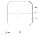
図1は、割断用太陽電池セル1000の構造を示す上面図である。図1に示すように、x軸、y軸、z軸を含む直交座標系が規定される。x軸、y軸は、割断用太陽電池セル1000の平面内において互いに直交する。z軸は、x軸およびy軸に垂直であり、割断用太陽電池セル1000の厚み方向に延びる。また、x軸、y軸、z軸のそれぞれの正の方向は、図1における矢印の方向に規定され、負の方向は、矢印と逆向きの方向に規定される。割断用太陽電池セル1000を形成する2つの主表面であって、かつx−y平面に平行な2つの主表面のうち、z軸の正方向側に配置される主平面が受光面であり、z軸の負方向側に配置される主平面が裏面である。以下では、z軸の正方向側を「受光面側」と呼び、z軸の負方向側を「裏面側」と呼ぶこともある。
(1) Manufacturing Procedure FIG. 1 is a top view showing the structure of the
そのため、図1は、受光面側からの割断用太陽電池セル1000の構造を示す。割断用太陽電池セル1000は、例えば、正方形の四隅を角面に面取りした形状を有する。割断用太陽電池セル1000のy軸方向の中央部分には、x軸方向に延びる割断線12が配置される。割断線12は、割断用太陽電池セル1000の割断が予定される線である。ここでは、割断用太陽電池セル1000を割断線12に沿って割断することによって、第1太陽電池セル10aと第2太陽電池セル10bが形成される。第1太陽電池セル10aと第2太陽電池セル10bは太陽電池セル10と総称され、太陽電池セル10は、y軸方向よりもx軸方向に長い矩形状を有する。このような太陽電池セル10はハーフカットセルとも呼ばれる。図1に示された割断用太陽電池セル1000の形状、割断線12の配置、太陽電池セル10の形状および数は、一例であり、これに限定されない。
Therefore, FIG. 1 shows the structure of the splitting
図2(a)−(f)は、割断用太陽電池セル1000の製造方法を示す。これらは、図1のA−A’線に沿った方向の部分断面図に相当する。図2(a)において、アズスライスシリコンウエハであるn型半導体基板100が用意される。n型半導体基板100は、例えば、単結晶や多結晶の構造を有するシリコン基板またはゲルマニウム基板等により形成されており、裏面側に第1面102を有し、受光面側に第2面104を有する。つまり、第1面102と第2面104は互いに反対側を向く。ここで、第1面102は、後述の処理においてpnヘテロ接合となる予定の方向である。
2 (a)-(f) show a method of manufacturing the
図2(b)において、ブレードダイシングあるいはレーザアブレーションによってn型半導体基板100の第1面102に溝部150が形成される。第1面102に配置される溝部150は、底面152と側面154とを含む。底面152は、第1面102あるいは第2面104に略平行な面であり、側面154は、第1面102と底面152とをつなぐ面である。ここで、第1面102と側面154とがなす角度θは90度以下にされる。つまり、溝部150は、アリ溝の形状の断面を有する。溝部150の幅は、例えば、0.01〜2mm、好ましくは0.02〜1mm、さらに好ましくは0.05〜0.5mmである。溝部150の幅が狭いほど、後述の処理において成膜がなされにくくなる。一方、溝部150の幅が広いほど、出力ロスが大きくなる。溝部150の深さは、例えば、0.01〜0.1mm、好ましくは0.02〜0.04mmである。溝部150の深さが浅いほど、後述の処理によって、未成膜領域が狭くなる。一方、溝部150の深さが深いほど、後述の処理において成膜がなされにくくなるとともに、セル化プロセス中に割れやすくなる。
In FIG. 2B, a
図2(c)において、n型半導体基板100に溝部150を形成した後に、洗浄、異方性エッチングにより、n型半導体基板100の第1面102と第2面104と、溝部150とにテクスチャ106が形成される。溝部150においては特に底面152にテクスチャ106が形成される。溝部150にテクスチャ106を形成する理由は、溝部150に進入した光の閉じ込め効果を高めるためである。
In FIG. 2C, after the
図2(d)において、テクスチャ106を形成した後に、溝部150が形成された第1面102の裏面側にp型パッシベーション層116がプラズマCVD(Chemical Vapor Deposition)法により形成される。その際、溝部150の底面152および側面154にもp型パッシベーション層116が形成される。これにより、n型半導体基板100の第1面102と、溝部150の底面152と側面154には、p型パッシベーション層116が重ねて配置される。p型パッシベーション層116は、真性非晶質半導体層とp型非晶質半導体層とを含み、これらのうちの真性非晶質半導体層が第1面102側に配置される。真性非晶質半導体層とp型非晶質半導体層は、例えば、シリコンあるいはゲルマニウム等により形成される。そのため、p型パッシベーション層116はp型の半導体材料を有するといえる。つまり、pn接合面が形成される側に溝部150が配置される。
In FIG. 2D, after the
また、第2面104の受光面側にn側パッシベーション層126がプラズマCVD法により形成される。これにより、n型半導体基板100の第2面104の受光面側には、n側パッシベーション層126が配置される。n側パッシベーション層126は、真性非晶質半導体層とn型非晶質半導体層とを含み、これらのうちの真性非晶質半導体層が第2面104側に配置される。真性非晶質半導体層とn型非晶質半導体層も、例えば、シリコンあるいはゲルマニウム等により形成される。そのため、n側パッシベーション層126は、n型の半導体材料を有するといえる。
Further, the n-
図2(e)において、溝部150が形成されたp型パッシベーション層116の裏面側にp側透明導電膜層114がPVD(Physical Vapor Deposition)法により形成される。p側透明導電膜層114は、ITO(Indium Tin Oxide)等の透光性の導電性膜であり、前述のTCOに相当する。一般的に、CVD法は表面マイグレーションにより対象物の形状に追随しやすいが、PVD法は対象物の形状に追随しにくい。そのため、p型パッシベーション層116は溝部150の底面152と側面154にも形成されるが、p側透明導電膜層114は、溝部150の底面152に形成され、側面154に形成されない。p側透明導電膜層114が形成されない側面154は、p側透明導電膜層114の未成膜領域160であるといえる。未成膜領域160では、p型パッシベーション層116のみが成膜される。つまり、p側透明導電膜層114を形成する前にn型半導体基板100に溝部150を形成することは、n型半導体基板100の形状によりマスクを形成することに相当する。このようなn型半導体基板100の形状によるマスクによって、未成膜領域160が形成される。さらに、p側透明導電膜層114の裏面側には、印刷プロセス等によりp側集電極(図示せず)が設けられる。p側集電極は、例えば銀電極である。
In FIG. 2E, a p-side transparent
また、n側パッシベーション層126の受光面側にn側透明導電膜層124がPVD法により形成される。n側透明導電膜層124も、ITO等の透光性の導電性膜であり、前述のTCOに相当する。さらに、n側透明導電膜層124の受光面側には、印刷プロセス等によりn側集電極(図示せず)が設けられる。n側集電極は、例えば銀電極である。p側透明導電膜層114あるいはn側透明導電膜層124の厚みは、例えば、1nm〜1μm、好ましくは50nm〜150nmであり、n型半導体基板100の厚みは、例えば、50μm〜500μm、好ましくは100μm〜200μmである。
Further, the n-side transparent
図2(b)において形成される溝部150が狭かったり、深かったりする場合、割断用太陽電池セル1000の構造は、図2(e)の代わりに図2(f)になる。図示のごとく、p型パッシベーション層116は、溝部150の側面154に形成されない。そのため、未成膜領域160には、p側透明導電膜層114、p型パッシベーション層116とが配置されない。
When the
以下では、割断用太陽電池セル1000が図2(e)の構造を有することを前提として、割断用太陽電池セル1000を割断する処理を説明する。図3(a)−(c)は、太陽電池セル10の製造方法を示す。割断は、図3(a)−(c)のいずれかによってなされる。図3(a)において、n側集電極およびp側集電極が形成された後、割断用太陽電池セル1000の第2面104側に、ブレードダイシングあるいはレーザアブレーションによって、割断溝200が形成される。溝部150が配置される面とは反対側の面からダイシング加工がなされるので、位置がずれても側面154へのダメージが生じない。割断溝200の幅は、例えば0.001〜1mm、好ましくは0.001〜0.5mm、さらに好ましくは0.001〜0.1mmである。特に、割断溝200の幅は溝部150の幅よりも狭くされる。割断溝200の幅が狭いほど外観の悪化が小さくなる。一方、割断溝200の幅が広いほど出力ロスが大きくなる。そのため、割断溝200の幅は狭いほうが好ましい。
Hereinafter, the process of splitting the split
割断溝200の深さは、例えば、0.01〜0.1mm、好ましくは0.02〜0.04mmである。割断溝200の深さが深いほど割断しやすくなる。走査回数を増やすことによって、適度な深さにされればよい。溝部150と割断溝200の深さの合計は、n型半導体基板100の厚み全体の40%〜80%、好ましくは50%〜70%にされる。さらに、割断溝200に含まれる割断線12に沿って割断用太陽電池セル1000が割断されることによって、第1太陽電池セル10aと第2太陽電池セル10bが製造される。
The depth of the
図3(b)において、n側集電極およびp側集電極が形成された後、溝部150の底面152に、ブレードダイシングあるいはレーザアブレーションによって、割断溝200が形成される。溝部150に対してダイシング加工がなされるので、受光面からの外観が維持される。割断溝200のサイズは、図3(a)と同一でよい。割断溝200に含まれる割断線12に沿って割断用太陽電池セル1000が割断されることによって、第1太陽電池セル10aと第2太陽電池セル10bが製造される。
In FIG. 3B, after the n-side collecting electrode and the p-side collecting electrode are formed, the
図3(c)において、n側集電極およびp側集電極が形成された後、TLS(Thermal Laser Separation)によって、割断線12に沿って割断用太陽電池セル1000が割断されて、第1太陽電池セル10aと第2太陽電池セル10bが製造される。
In FIG. 3C, after the n-side collecting electrode and the p-side collecting electrode are formed, the dividing
(2)太陽電池モジュールの構造
図4(a)−(c)は、太陽電池セル10を含む太陽電池モジュール50の構造を示す。図4(a)は、太陽電池モジュール50の受光面側からの平面図である。太陽電池モジュール50では、太陽電池パネル60の周囲を囲むようにフレームが取り付けられる。太陽電池パネル60は、太陽電池セル10と総称される第11太陽電池セル10aa、・・・、第44太陽電池セル10dd、ストリング間配線材22、ストリング端配線材24、セル間配線材26を含む。
(2) Structure of Solar Cell Module FIGS. 4 (a)-(c) show the structure of the
各太陽電池セル10は、これまで説明した割断用太陽電池セル1000の割断により生成される。また、各太陽電池セル10の受光面および裏面には、互いに平行にx軸方向に延びる複数のフィンガー電極と、複数のフィンガー電極に直交するようにy軸方向に延びる複数、例えば2本のバスバー電極とが備えられる。バスバー電極は、複数のフィンガー電極のそれぞれを接続する。また、バスバー電極およびフィンガー電極は、前述のp側集電極およびn側集電極に相当する。
Each solar cell 10 is generated by the splitting of the splitting
複数の太陽電池セル10は、x−y平面上にマトリクス状に配列される。ここでは、一例として、x軸方向に4つの太陽電池セル10が並べられ、y軸方向に4つの太陽電池セル10が並べられる。x軸方向に並べられる太陽電池セル10の数と、y軸方向に並べられる太陽電池セル10の数は、これに限定されない。y軸方向に並んで配置される4つの太陽電池セル10は、セル間配線材26によって直列に接続され、1つの太陽電池ストリング20を形成する。例えば、第11太陽電池セル10aa、第12太陽電池セル10ab、第13太陽電池セル10ac、第14太陽電池セル10adが接続されることによって、第1太陽電池ストリング20aが形成される。他の太陽電池ストリング20、例えば、第2太陽電池ストリング20bから第4太陽電池ストリング20dも同様に形成される。その結果、4つの太陽電池ストリング20がx軸方向に平行に並べられる。
The plurality of solar cell 10s are arranged in a matrix on the xy plane. Here, as an example, four solar cells 10 are arranged in the x-axis direction, and four solar cells 10 are arranged in the y-axis direction. The number of solar cells 10 arranged in the x-axis direction and the number of solar cells 10 arranged in the y-axis direction are not limited to this. The four solar cells 10 arranged side by side in the y-axis direction are connected in series by the
太陽電池ストリング20を形成するために、セル間配線材26は、隣接した太陽電池セル10のうちの一方の受光面側のバスバー電極と、他方の裏面側のバスバー電極とを接続する。例えば、第11太陽電池セル10aaと第12太陽電池セル10abとを接続するための2つのセル間配線材26は、第11太陽電池セル10aaの受光面側のバスバー電極と第12太陽電池セル10abの裏面側のバスバー電極とを電気的に接続する。
In order to form the solar cell string 20, the
複数のストリング間配線材22のそれぞれは、x軸方向に延びて、互いに隣接する2つの太陽電池ストリング20に電気的に接続される。例えば、複数の太陽電池セル10よりもy軸の正方向に配置されるストリング間配線材22は、第2太陽電池ストリング20bにおける第21太陽電池セル10baと、第3太陽電池ストリング20cにおける第31太陽電池セル10caとを接続する。他のストリング間配線材22も同様である。その結果、複数の太陽電池ストリング20は直列に接続される。直列に接続された複数の太陽電池ストリング20の両端の太陽電池セル10、例えば、第11太陽電池セル10aaと第41太陽電池セル10daには、ストリング端配線材24が接続される。ストリング端配線材24は、図示しない端子ボックスに接続される。
Each of the plurality of
図4(b)は、太陽電池モジュール50の断面図であり、図4(a)のB−B’断面図である。太陽電池モジュール50における太陽電池パネル60は、太陽電池セル10と総称される第11太陽電池セル10aa、第12太陽電池セル10ab、第13太陽電池セル10ac、セル間配線材26、保護部材40と総称される第1保護部材40a、第2保護部材40b、封止部材42と総称される第1封止部材42a、第2封止部材42bを含む。図4(a)の上側が受光面側に相当し、下側が裏面側に相当する。
FIG. 4B is a cross-sectional view of the
第1保護部材40aは、太陽電池パネル60の受光面側に配置されており、太陽電池パネル60の表面を保護する。第1保護部材40aには、透光性および遮水性を有するガラス、透光性プラスチック等が使用され、矩形板状に形成される。ここでは、一例としてガラスが使用されるとする。第1封止部材42aは、第1保護部材40aの裏面側に積層される。第1封止部材42aは、第1保護部材40aと太陽電池セル10との間に配置されて、これらを接着する。第1封止部材42aとして、例えば、ポリオレフィン、EVA、PVB(ポリビニルブチラール)、ポリイミド等の樹脂フィルムのような熱可塑性樹脂が使用される。熱硬化性樹脂が使用されてもよい。第1封止部材42aは、透光性を有するとともに、第1保護部材40aにおけるx−y平面と略同一寸法の面を有する矩形状のシート材によって形成される。
The first
第2封止部材42bは、第1封止部材42aの裏面側に積層される。第2封止部材42bは、第1封止部材42aとの間で、複数の太陽電池セル10、セル間配線材26等を封止する。第2封止部材42bには、第1封止部材42aと同様のものを用いることができる。また、ラミネート・キュア工程における加熱によって、第2封止部材42bは第1封止部材42aと一体化されていてもよい。
The
第2保護部材40bは、第2封止部材42bの裏面側に積層される。第2保護部材40bは、バックシートとして太陽電池パネル60の裏面側を保護する。第2保護部材40bとしては、例えば、PET等の樹脂フィルムが使用される。第2保護部材40bとして、Al箔を樹脂フィルムで挟んだ構造を有する積層フィルムなどが使用されてもよい。
The second
図4(c)は、太陽電池モジュール50の裏面側からの平面図である。太陽電池モジュール50における太陽電池パネル60には、箱形形状の端子ボックス30が取り付けられる。端子ボックス30には、第1ケーブル32a、第2ケーブル32bが電気的に接続される。第1ケーブル32a、第2ケーブル32bは、太陽電池モジュール50において発電した電力を外部に出力する。
FIG. 4C is a plan view from the back surface side of the
本実施例によれば、n型半導体基板100に溝部150を形成してからp側透明導電膜層114を成膜するので、n型半導体基板100の形状によりマスク効果を得ることができる。また、n型半導体基板100の形状によりマスク効果が得られるので、未成膜領域160を形成できる。また、側面154の少なくとも一部には未成膜領域160が形成されるので、割断による発電の出力の低下を抑制できる。また、溝部150の底面152にもp側透明導電膜層114が形成されるので、p側透明導電膜層114の面積の減少を抑制できる。
According to this embodiment, since the
また、第1面102と溝部150の底面152とにp型パッシベーション層116が形成されるので、パッシベーション層を確保できる。また、側面154にもp型パッシベーション層116が形成されるので、パッシベーション層を確保できる。また、n型半導体基板100の第1面102と、溝部150とにテクスチャ106を形成するので、太陽電池セル10に入射した光を有効に利用できる。また、太陽電池セル10に入射した光が有効に利用されるので、発電効率を向上できる。また、溝部150にテクスチャ106を形成するので、光の閉じ込め効果を高めることができる。また、光の閉じ込め効果が高まるので、出力を向上できる。
Further, since the p-
また、溝部150の底面152に形成した割断溝200に沿って割断するので、受光面から割断溝200を見えなくできる。また、受光面から割断溝200が見えなくなるので、受光面側からの外観を悪化させないように割断できる。また、溝部150に割断溝200を加工するので、加工の位置精度を向上できる。また、n型半導体基板100における第1面102と反対を向いた第2面104に形成した割断溝200に沿って割断するので、側面154へのダメージを抑制できる。また、受光面側に割断溝200を設けるので、割断溝200とpn接合部分との距離を長くできる。また、割断溝200とpn接合部分との距離が長くなるので、加工の影響を低減できる。
Further, since the
本実施例の概要は、次の通りである。本開示のある態様の太陽電池セル10の製造方法は、n型半導体基板100の第1面102に溝部150を形成するステップと、溝部150が形成されたn型半導体基板100の第1面102にp側透明導電膜層114を形成するステップとを備える。溝部150の側面154の少なくとも一部には、p側透明導電膜層114の未成膜領域160が形成される。
The outline of this embodiment is as follows. The method for manufacturing the solar cell 10 according to an aspect of the present disclosure includes a step of forming a
溝部150の底面152にもp側透明導電膜層114が形成される。
The p-side transparent
p側透明導電膜層114を形成するステップの前に、溝部150が形成されたn型半導体基板100の第1面102にp型パッシベーション層116を形成するステップをさらに備えてもよい。溝部150の底面152にもp型パッシベーション層116が形成される。
Prior to the step of forming the p-side transparent
溝部150の側面154の少なくとも一部にもp型パッシベーション層116が形成される。
A p-
p型パッシベーション層116を形成するステップの前に、n型半導体基板100の第1面102と、溝部150とにテクスチャ106を形成するステップをさらに備える。
Prior to the step of forming the p-
溝部150の底面152に割断溝200を形成するステップと、割断溝200に沿って割断するステップと、をさらに備える。
A step of forming the
n型半導体基板100における第1面102と反対を向いた第2面104に割断溝200を形成するステップと、割断溝200に沿って割断するステップと、をさらに備える。
The n-
本開示の別の態様は、割断用太陽電池セル1000である。この割断用太陽電池セル1000は、n型半導体基板100と、n型半導体基板100の第1面102に配置される溝部150と、n型半導体基板100の第1面102と溝部150の底面152とに少なくとも配置されるp型パッシベーション層116と、n型半導体基板100の第1面102と溝部150の底面152とにおいて、p型パッシベーション層116に重ねて配置されるp側透明導電膜層114とを備える。溝部150の側面154の少なくとも一部には、p側透明導電膜層114の未成膜領域160が配置される。
Another aspect of the present disclosure is a splitting
溝部150の側面154の少なくとも一部にもp型パッシベーション層116が配置される。
The p-
n型半導体基板100は、溝部150の底面152にテクスチャ構造を有する。
The n-
以上、本開示について実施例をもとに説明した。この実施例は例示であり、それらの各構成要素あるいは各処理プロセスの組合せにいろいろな変形例が可能なこと、またそうした変形例も本開示の範囲にあることは当業者に理解されるところである。 The present disclosure has been described above based on examples. This embodiment is an example, and it will be understood by those skilled in the art that various modifications are possible for each of these components or combinations of each processing process, and that such modifications are also within the scope of the present disclosure. ..
10 太陽電池セル、 12 割断線、 20 太陽電池ストリング、 22 ストリング間配線材、 24 ストリング端配線材、 26 セル間配線材、 30 端子ボックス、 32 ケーブル、 40 保護部材、 42 封止部材、 50 太陽電池モジュール、 60 太陽電池パネル、 100 n型半導体基板、 102 第1面(表面)、 104 第2面、 106 テクスチャ、 114 p側透明導電膜層、 116 p型パッシベーション層(非晶質半導体層)、 124 n側透明導電膜層、 126 n側パッシベーション層、 150 溝部、 152 底面、 154 側面、 160 未成膜領域、 200 割断溝、 1000 割断用太陽電池セル。 10 Solar cell, 12 Broken wire, 20 Solar cell string, 22 String-to-string wiring material, 24 String-end wiring material, 26 Cell-to-cell wiring material, 30 Terminal box, 32 Cable, 40 Protective member, 42 Sealing member, 50 Solar Battery module, 60 solar cell panel, 100 n type semiconductor substrate, 102 first surface (surface), 104 second surface, 106 texture, 114 p side transparent conductive film layer, 116 p type passion layer (amorphous semiconductor layer) , 124 n-side transparent conductive film layer, 126 n-side passivation layer, 150 groove, 152 bottom surface, 154 side surface, 160 undeposited area, 200 split groove, 1000 split solar cell.
Claims (10)
前記溝部が形成された前記半導体基板の前記表面に透明導電膜層を形成するステップとを備え、
前記溝部の側面の少なくとも一部には、前記透明導電膜層の未成膜領域が形成される、
太陽電池セルの製造方法。 Steps to form grooves on the surface of the semiconductor substrate,
A step of forming a transparent conductive film layer on the surface of the semiconductor substrate on which the groove is formed is provided.
An unfilmed region of the transparent conductive film layer is formed on at least a part of the side surface of the groove.
How to manufacture solar cells.
請求項1に記載の太陽電池セルの製造方法。 The transparent conductive film layer is also formed on the bottom surface of the groove.
The method for manufacturing a solar cell according to claim 1.
前記溝部の底面にも前記非晶質半導体層が形成される、
請求項1または2に記載の太陽電池セルの製造方法。 A step of forming an amorphous semiconductor layer on the surface of the semiconductor substrate on which the groove is formed is further provided before the step of forming the transparent conductive film layer.
The amorphous semiconductor layer is also formed on the bottom surface of the groove.
The method for manufacturing a solar cell according to claim 1 or 2.
請求項3に記載の太陽電池セルの製造方法。 The amorphous semiconductor layer is also formed on at least a part of the side surface of the groove.
The method for manufacturing a solar cell according to claim 3.
請求項3または4に記載の太陽電池セルの製造方法。 Prior to the step of forming the amorphous semiconductor layer, a step of forming a texture on the surface of the semiconductor substrate and the groove portion is further provided.
The method for manufacturing a solar cell according to claim 3 or 4.
前記割断溝に沿って割断するステップと、
をさらに備える請求項1から5のいずれか1項に記載の太陽電池セルの製造方法。 The step of forming a split groove on the bottom surface of the groove,
The step of cutting along the cutting groove and
The method for manufacturing a solar cell according to any one of claims 1 to 5, further comprising.
前記割断溝に沿って割断するステップと、
をさらに備える請求項1から5のいずれか1項に記載の太陽電池セルの製造方法。 A step of forming a split groove on a second surface of the semiconductor substrate facing away from the first surface, wherein the surface is the first surface.
The step of cutting along the cutting groove and
The method for manufacturing a solar cell according to any one of claims 1 to 5, further comprising.
前記半導体基板の表面に配置される溝部と、
前記半導体基板の表面と前記溝部の底面とに少なくとも配置される非晶質半導体層と、
前記半導体基板の表面と前記溝部の底面とにおいて、前記非晶質半導体層に重ねて配置される透明導電膜層とを備え、
前記溝部の側面の少なくとも一部には、前記透明導電膜層の未成膜領域が配置される、
割断用太陽電池セル。 With a semiconductor substrate
Grooves arranged on the surface of the semiconductor substrate and
An amorphous semiconductor layer arranged at least on the surface of the semiconductor substrate and the bottom surface of the groove, and
A transparent conductive film layer arranged on the amorphous semiconductor layer on the surface of the semiconductor substrate and the bottom surface of the groove is provided.
An unfilmed region of the transparent conductive film layer is arranged on at least a part of the side surface of the groove.
Solar cell for splitting.
請求項8に記載の割断用太陽電池セル。 The amorphous semiconductor layer is also arranged on at least a part of the side surface of the groove.
The solar cell for splitting according to claim 8.
Priority Applications (3)
| Application Number | Priority Date | Filing Date | Title |
|---|---|---|---|
| JP2019061114A JP7278831B2 (en) | 2019-03-27 | 2019-03-27 | SOLAR BATTERY CELL MANUFACTURING METHOD AND CUTTING SOLAR BATTERY CELL |
| US16/831,537 US11257968B2 (en) | 2019-03-27 | 2020-03-26 | Method of manufacturing solar cell and splittable solar cell for manufacturing solar cell from splittable solar cell that can be split |
| CN202010227378.0A CN111755562A (en) | 2019-03-27 | 2020-03-27 | Method for manufacturing solar cell and solar cell for dicing |
Applications Claiming Priority (1)
| Application Number | Priority Date | Filing Date | Title |
|---|---|---|---|
| JP2019061114A JP7278831B2 (en) | 2019-03-27 | 2019-03-27 | SOLAR BATTERY CELL MANUFACTURING METHOD AND CUTTING SOLAR BATTERY CELL |
Publications (2)
| Publication Number | Publication Date |
|---|---|
| JP2020161702A true JP2020161702A (en) | 2020-10-01 |
| JP7278831B2 JP7278831B2 (en) | 2023-05-22 |
Family
ID=72604957
Family Applications (1)
| Application Number | Title | Priority Date | Filing Date |
|---|---|---|---|
| JP2019061114A Active JP7278831B2 (en) | 2019-03-27 | 2019-03-27 | SOLAR BATTERY CELL MANUFACTURING METHOD AND CUTTING SOLAR BATTERY CELL |
Country Status (3)
| Country | Link |
|---|---|
| US (1) | US11257968B2 (en) |
| JP (1) | JP7278831B2 (en) |
| CN (1) | CN111755562A (en) |
Cited By (1)
| Publication number | Priority date | Publication date | Assignee | Title |
|---|---|---|---|---|
| CN115548144A (en) * | 2022-11-04 | 2022-12-30 | 安徽华晟新能源科技有限公司 | Semiconductor substrate and processing method thereof, solar cell and preparation method thereof |
Families Citing this family (3)
| Publication number | Priority date | Publication date | Assignee | Title |
|---|---|---|---|---|
| JP7278831B2 (en) * | 2019-03-27 | 2023-05-22 | パナソニックホールディングス株式会社 | SOLAR BATTERY CELL MANUFACTURING METHOD AND CUTTING SOLAR BATTERY CELL |
| CN113380926B (en) * | 2021-06-11 | 2023-02-10 | 安徽华晟新能源科技有限公司 | Manufacturing method of heterojunction solar cell and heterojunction solar cell |
| DE102021121684A1 (en) * | 2021-08-20 | 2023-02-23 | Fraunhofer-Gesellschaft zur Förderung der angewandten Forschung eingetragener Verein | Process for dicing semiconductor components |
Citations (5)
| Publication number | Priority date | Publication date | Assignee | Title |
|---|---|---|---|---|
| JP2003101053A (en) * | 2001-09-27 | 2003-04-04 | Sanyo Electric Co Ltd | Solar battery device and manufacturing method therefor |
| JP2005050925A (en) * | 2003-07-30 | 2005-02-24 | Kyocera Corp | Method for manufacturing solar battery element |
| US20150179858A1 (en) * | 2013-12-25 | 2015-06-25 | Neo Solar Power Corp. | Solar cell and manufacturing method thereof |
| JP2015191962A (en) * | 2014-03-27 | 2015-11-02 | 三菱電機株式会社 | Solar cell and manufacturing method therefor |
| JP2015198142A (en) * | 2014-03-31 | 2015-11-09 | 株式会社カネカ | Crystal silicon solar battery, manufacturing method for the same and solar battery module |
Family Cites Families (11)
| Publication number | Priority date | Publication date | Assignee | Title |
|---|---|---|---|---|
| US5391235A (en) * | 1992-03-31 | 1995-02-21 | Canon Kabushiki Kaisha | Solar cell module and method of manufacturing the same |
| US7879685B2 (en) * | 2006-08-04 | 2011-02-01 | Solyndra, Inc. | System and method for creating electric isolation between layers comprising solar cells |
| NL2004065C2 (en) * | 2010-01-06 | 2011-07-07 | Stichting Energie | Solar panel module and method for manufacturing such a solar panel module. |
| JP5845445B2 (en) * | 2010-01-26 | 2016-01-20 | パナソニックIpマネジメント株式会社 | Solar cell and manufacturing method thereof |
| JP5535709B2 (en) * | 2010-03-19 | 2014-07-02 | 三洋電機株式会社 | SOLAR CELL, SOLAR CELL MODULE USING THE SOLAR CELL, AND SOLAR CELL MANUFACTURING METHOD |
| US8134217B2 (en) * | 2010-12-14 | 2012-03-13 | Sunpower Corporation | Bypass diode for a solar cell |
| JP2014239085A (en) | 2011-10-03 | 2014-12-18 | 三菱電機株式会社 | Solar battery element and method of manufacturing the same |
| US20150270422A1 (en) * | 2012-10-02 | 2015-09-24 | Kaneka Corporation | Method for producing crystalline silicon solar cell, method for producing solar cell module, crystalline silicon solar cell, and solar cell module |
| JP2015053303A (en) * | 2013-09-05 | 2015-03-19 | シャープ株式会社 | Solar cell, solar cell module, and method for manufacturing solar cell |
| WO2018084159A1 (en) * | 2016-11-02 | 2018-05-11 | 株式会社カネカ | Solar cell, method for manufacturing same, and solar cell module |
| JP7278831B2 (en) * | 2019-03-27 | 2023-05-22 | パナソニックホールディングス株式会社 | SOLAR BATTERY CELL MANUFACTURING METHOD AND CUTTING SOLAR BATTERY CELL |
-
2019
- 2019-03-27 JP JP2019061114A patent/JP7278831B2/en active Active
-
2020
- 2020-03-26 US US16/831,537 patent/US11257968B2/en active Active
- 2020-03-27 CN CN202010227378.0A patent/CN111755562A/en active Pending
Patent Citations (5)
| Publication number | Priority date | Publication date | Assignee | Title |
|---|---|---|---|---|
| JP2003101053A (en) * | 2001-09-27 | 2003-04-04 | Sanyo Electric Co Ltd | Solar battery device and manufacturing method therefor |
| JP2005050925A (en) * | 2003-07-30 | 2005-02-24 | Kyocera Corp | Method for manufacturing solar battery element |
| US20150179858A1 (en) * | 2013-12-25 | 2015-06-25 | Neo Solar Power Corp. | Solar cell and manufacturing method thereof |
| JP2015191962A (en) * | 2014-03-27 | 2015-11-02 | 三菱電機株式会社 | Solar cell and manufacturing method therefor |
| JP2015198142A (en) * | 2014-03-31 | 2015-11-09 | 株式会社カネカ | Crystal silicon solar battery, manufacturing method for the same and solar battery module |
Cited By (2)
| Publication number | Priority date | Publication date | Assignee | Title |
|---|---|---|---|---|
| CN115548144A (en) * | 2022-11-04 | 2022-12-30 | 安徽华晟新能源科技有限公司 | Semiconductor substrate and processing method thereof, solar cell and preparation method thereof |
| CN115548144B (en) * | 2022-11-04 | 2024-05-07 | 安徽华晟新能源科技有限公司 | Semiconductor substrate and processing method thereof, solar cell and preparation method thereof |
Also Published As
| Publication number | Publication date |
|---|---|
| US20200313011A1 (en) | 2020-10-01 |
| CN111755562A (en) | 2020-10-09 |
| JP7278831B2 (en) | 2023-05-22 |
| US11257968B2 (en) | 2022-02-22 |
Similar Documents
| Publication | Publication Date | Title |
|---|---|---|
| JP7278831B2 (en) | SOLAR BATTERY CELL MANUFACTURING METHOD AND CUTTING SOLAR BATTERY CELL | |
| US20190393361A1 (en) | Solar panel | |
| JP2013008785A (en) | Solar cell module | |
| KR20180072110A (en) | Solar cell and solar cell panel including the same | |
| JP2013048166A (en) | Solar cell module, solar cell module array, and manufacturing method of solar cell module | |
| JP7085613B2 (en) | Manufacturing method of solar cell module, glass building material, and solar cell module | |
| WO2018001187A1 (en) | Battery cell, battery cell matrix, solar cell, and battery cell preparation method | |
| JP2013143529A (en) | Solar cell module | |
| JP2017174986A (en) | Solar battery cell and solar battery module | |
| KR101788160B1 (en) | Solar cell module | |
| JP2011249736A (en) | Solar cell module manufacturing method | |
| KR101806972B1 (en) | Solar cell module | |
| JP2020161701A (en) | Manufacturing method of solar cell, solar cell, and solar cell module | |
| WO2013042417A1 (en) | Solar cell module and solar cell | |
| JP2020161545A (en) | Solar cell for splitting and solar cell | |
| KR20190043295A (en) | Stile type solar cell module using divided cell | |
| WO2021106417A1 (en) | Photovoltaic cell, photovoltaic cell module, and method for manufacturing photovoltaic cell | |
| JP2018074125A (en) | Solar battery cell, solar battery module, and method for manufacturing solar battery cell | |
| JP5244842B2 (en) | Method for manufacturing thin film solar cell | |
| US20220302332A1 (en) | Unit cell, solar cell comprising same, and method for manufacturing solar cell | |
| WO2020158379A1 (en) | Solar cell string | |
| JP6681607B2 (en) | Solar cell and method for manufacturing solar cell | |
| KR102379388B1 (en) | Solar cell and solar cell panel including the same | |
| JP2009231499A (en) | Photoelectric conversion device | |
| KR101816180B1 (en) | Solar cell module |
Legal Events
| Date | Code | Title | Description |
|---|---|---|---|
| A621 | Written request for application examination |
Free format text: JAPANESE INTERMEDIATE CODE: A621 Effective date: 20220112 |
|
| A977 | Report on retrieval |
Free format text: JAPANESE INTERMEDIATE CODE: A971007 Effective date: 20221012 |
|
| A131 | Notification of reasons for refusal |
Free format text: JAPANESE INTERMEDIATE CODE: A131 Effective date: 20221018 |
|
| A521 | Request for written amendment filed |
Free format text: JAPANESE INTERMEDIATE CODE: A523 Effective date: 20221212 |
|
| A131 | Notification of reasons for refusal |
Free format text: JAPANESE INTERMEDIATE CODE: A131 Effective date: 20230110 |
|
| A521 | Request for written amendment filed |
Free format text: JAPANESE INTERMEDIATE CODE: A523 Effective date: 20230228 |
|
| TRDD | Decision of grant or rejection written | ||
| A01 | Written decision to grant a patent or to grant a registration (utility model) |
Free format text: JAPANESE INTERMEDIATE CODE: A01 Effective date: 20230411 |
|
| A61 | First payment of annual fees (during grant procedure) |
Free format text: JAPANESE INTERMEDIATE CODE: A61 Effective date: 20230510 |
|
| R151 | Written notification of patent or utility model registration |
Ref document number: 7278831 Country of ref document: JP Free format text: JAPANESE INTERMEDIATE CODE: R151 |