JP2020161701A - Manufacturing method of solar cell, solar cell, and solar cell module - Google Patents
Manufacturing method of solar cell, solar cell, and solar cell module Download PDFInfo
- Publication number
- JP2020161701A JP2020161701A JP2019061113A JP2019061113A JP2020161701A JP 2020161701 A JP2020161701 A JP 2020161701A JP 2019061113 A JP2019061113 A JP 2019061113A JP 2019061113 A JP2019061113 A JP 2019061113A JP 2020161701 A JP2020161701 A JP 2020161701A
- Authority
- JP
- Japan
- Prior art keywords
- solar cell
- conductive type
- semiconductor layer
- type
- type semiconductor
- Prior art date
- Legal status (The legal status is an assumption and is not a legal conclusion. Google has not performed a legal analysis and makes no representation as to the accuracy of the status listed.)
- Pending
Links
- 238000004519 manufacturing process Methods 0.000 title claims description 32
- 239000002019 doping agent Substances 0.000 claims abstract description 45
- 239000004065 semiconductor Substances 0.000 claims description 156
- 239000000758 substrate Substances 0.000 claims description 54
- 238000005520 cutting process Methods 0.000 claims description 36
- 239000012535 impurity Substances 0.000 claims description 21
- 238000000034 method Methods 0.000 claims description 19
- 230000001678 irradiating effect Effects 0.000 claims description 14
- 230000007423 decrease Effects 0.000 abstract description 9
- 238000010248 power generation Methods 0.000 abstract description 6
- 238000005516 engineering process Methods 0.000 abstract 1
- 239000010408 film Substances 0.000 description 16
- 239000000463 material Substances 0.000 description 16
- 238000007789 sealing Methods 0.000 description 16
- 238000002161 passivation Methods 0.000 description 15
- 230000001681 protective effect Effects 0.000 description 14
- 230000005685 electric field effect Effects 0.000 description 12
- 239000007789 gas Substances 0.000 description 11
- 238000010586 diagram Methods 0.000 description 5
- 238000010030 laminating Methods 0.000 description 4
- 229920005989 resin Polymers 0.000 description 4
- 239000011347 resin Substances 0.000 description 4
- 238000013459 approach Methods 0.000 description 3
- 230000007547 defect Effects 0.000 description 3
- 230000000694 effects Effects 0.000 description 3
- 239000007790 solid phase Substances 0.000 description 3
- 239000013078 crystal Substances 0.000 description 2
- 230000002950 deficient Effects 0.000 description 2
- 230000005669 field effect Effects 0.000 description 2
- 239000011521 glass Substances 0.000 description 2
- 230000002779 inactivation Effects 0.000 description 2
- 238000003698 laser cutting Methods 0.000 description 2
- 238000012986 modification Methods 0.000 description 2
- 230000004048 modification Effects 0.000 description 2
- 229920002037 poly(vinyl butyral) polymer Polymers 0.000 description 2
- 239000002243 precursor Substances 0.000 description 2
- 239000012808 vapor phase Substances 0.000 description 2
- 239000004642 Polyimide Substances 0.000 description 1
- 238000005452 bending Methods 0.000 description 1
- 230000015572 biosynthetic process Effects 0.000 description 1
- 239000000969 carrier Substances 0.000 description 1
- 229910021419 crystalline silicon Inorganic materials 0.000 description 1
- 230000006866 deterioration Effects 0.000 description 1
- 239000008393 encapsulating agent Substances 0.000 description 1
- 239000011888 foil Substances 0.000 description 1
- 238000010438 heat treatment Methods 0.000 description 1
- 125000004435 hydrogen atom Chemical group [H]* 0.000 description 1
- AMGQUBHHOARCQH-UHFFFAOYSA-N indium;oxotin Chemical compound [In].[Sn]=O AMGQUBHHOARCQH-UHFFFAOYSA-N 0.000 description 1
- 239000011159 matrix material Substances 0.000 description 1
- 239000012071 phase Substances 0.000 description 1
- RLOWWWKZYUNIDI-UHFFFAOYSA-N phosphinic chloride Chemical compound ClP=O RLOWWWKZYUNIDI-UHFFFAOYSA-N 0.000 description 1
- 229920003023 plastic Polymers 0.000 description 1
- 239000004033 plastic Substances 0.000 description 1
- 229920001200 poly(ethylene-vinyl acetate) Polymers 0.000 description 1
- 229920001721 polyimide Polymers 0.000 description 1
- 229920000098 polyolefin Polymers 0.000 description 1
- 238000005215 recombination Methods 0.000 description 1
- 230000006798 recombination Effects 0.000 description 1
- 229910052710 silicon Inorganic materials 0.000 description 1
- 239000010703 silicon Substances 0.000 description 1
- 229920005992 thermoplastic resin Polymers 0.000 description 1
- 229920001187 thermosetting polymer Polymers 0.000 description 1
- 239000010409 thin film Substances 0.000 description 1
- XLYOFNOQVPJJNP-UHFFFAOYSA-N water Substances O XLYOFNOQVPJJNP-UHFFFAOYSA-N 0.000 description 1
Images


Classifications
-
- H—ELECTRICITY
- H01—ELECTRIC ELEMENTS
- H01L—SEMICONDUCTOR DEVICES NOT COVERED BY CLASS H10
- H01L31/00—Semiconductor devices sensitive to infrared radiation, light, electromagnetic radiation of shorter wavelength or corpuscular radiation and specially adapted either for the conversion of the energy of such radiation into electrical energy or for the control of electrical energy by such radiation; Processes or apparatus specially adapted for the manufacture or treatment thereof or of parts thereof; Details thereof
- H01L31/04—Semiconductor devices sensitive to infrared radiation, light, electromagnetic radiation of shorter wavelength or corpuscular radiation and specially adapted either for the conversion of the energy of such radiation into electrical energy or for the control of electrical energy by such radiation; Processes or apparatus specially adapted for the manufacture or treatment thereof or of parts thereof; Details thereof adapted as photovoltaic [PV] conversion devices
- H01L31/06—Semiconductor devices sensitive to infrared radiation, light, electromagnetic radiation of shorter wavelength or corpuscular radiation and specially adapted either for the conversion of the energy of such radiation into electrical energy or for the control of electrical energy by such radiation; Processes or apparatus specially adapted for the manufacture or treatment thereof or of parts thereof; Details thereof adapted as photovoltaic [PV] conversion devices characterised by potential barriers
- H01L31/072—Semiconductor devices sensitive to infrared radiation, light, electromagnetic radiation of shorter wavelength or corpuscular radiation and specially adapted either for the conversion of the energy of such radiation into electrical energy or for the control of electrical energy by such radiation; Processes or apparatus specially adapted for the manufacture or treatment thereof or of parts thereof; Details thereof adapted as photovoltaic [PV] conversion devices characterised by potential barriers the potential barriers being only of the PN heterojunction type
- H01L31/0745—Semiconductor devices sensitive to infrared radiation, light, electromagnetic radiation of shorter wavelength or corpuscular radiation and specially adapted either for the conversion of the energy of such radiation into electrical energy or for the control of electrical energy by such radiation; Processes or apparatus specially adapted for the manufacture or treatment thereof or of parts thereof; Details thereof adapted as photovoltaic [PV] conversion devices characterised by potential barriers the potential barriers being only of the PN heterojunction type comprising a AIVBIV heterojunction, e.g. Si/Ge, SiGe/Si or Si/SiC solar cells
- H01L31/0747—Semiconductor devices sensitive to infrared radiation, light, electromagnetic radiation of shorter wavelength or corpuscular radiation and specially adapted either for the conversion of the energy of such radiation into electrical energy or for the control of electrical energy by such radiation; Processes or apparatus specially adapted for the manufacture or treatment thereof or of parts thereof; Details thereof adapted as photovoltaic [PV] conversion devices characterised by potential barriers the potential barriers being only of the PN heterojunction type comprising a AIVBIV heterojunction, e.g. Si/Ge, SiGe/Si or Si/SiC solar cells comprising a heterojunction of crystalline and amorphous materials, e.g. heterojunction with intrinsic thin layer
-
- H—ELECTRICITY
- H01—ELECTRIC ELEMENTS
- H01L—SEMICONDUCTOR DEVICES NOT COVERED BY CLASS H10
- H01L31/00—Semiconductor devices sensitive to infrared radiation, light, electromagnetic radiation of shorter wavelength or corpuscular radiation and specially adapted either for the conversion of the energy of such radiation into electrical energy or for the control of electrical energy by such radiation; Processes or apparatus specially adapted for the manufacture or treatment thereof or of parts thereof; Details thereof
- H01L31/18—Processes or apparatus specially adapted for the manufacture or treatment of these devices or of parts thereof
- H01L31/1876—Particular processes or apparatus for batch treatment of the devices
-
- H—ELECTRICITY
- H01—ELECTRIC ELEMENTS
- H01L—SEMICONDUCTOR DEVICES NOT COVERED BY CLASS H10
- H01L31/00—Semiconductor devices sensitive to infrared radiation, light, electromagnetic radiation of shorter wavelength or corpuscular radiation and specially adapted either for the conversion of the energy of such radiation into electrical energy or for the control of electrical energy by such radiation; Processes or apparatus specially adapted for the manufacture or treatment thereof or of parts thereof; Details thereof
- H01L31/0248—Semiconductor devices sensitive to infrared radiation, light, electromagnetic radiation of shorter wavelength or corpuscular radiation and specially adapted either for the conversion of the energy of such radiation into electrical energy or for the control of electrical energy by such radiation; Processes or apparatus specially adapted for the manufacture or treatment thereof or of parts thereof; Details thereof characterised by their semiconductor bodies
- H01L31/0352—Semiconductor devices sensitive to infrared radiation, light, electromagnetic radiation of shorter wavelength or corpuscular radiation and specially adapted either for the conversion of the energy of such radiation into electrical energy or for the control of electrical energy by such radiation; Processes or apparatus specially adapted for the manufacture or treatment thereof or of parts thereof; Details thereof characterised by their semiconductor bodies characterised by their shape or by the shapes, relative sizes or disposition of the semiconductor regions
- H01L31/035272—Semiconductor devices sensitive to infrared radiation, light, electromagnetic radiation of shorter wavelength or corpuscular radiation and specially adapted either for the conversion of the energy of such radiation into electrical energy or for the control of electrical energy by such radiation; Processes or apparatus specially adapted for the manufacture or treatment thereof or of parts thereof; Details thereof characterised by their semiconductor bodies characterised by their shape or by the shapes, relative sizes or disposition of the semiconductor regions characterised by at least one potential jump barrier or surface barrier
- H01L31/035281—Shape of the body
-
- H—ELECTRICITY
- H01—ELECTRIC ELEMENTS
- H01L—SEMICONDUCTOR DEVICES NOT COVERED BY CLASS H10
- H01L31/00—Semiconductor devices sensitive to infrared radiation, light, electromagnetic radiation of shorter wavelength or corpuscular radiation and specially adapted either for the conversion of the energy of such radiation into electrical energy or for the control of electrical energy by such radiation; Processes or apparatus specially adapted for the manufacture or treatment thereof or of parts thereof; Details thereof
- H01L31/04—Semiconductor devices sensitive to infrared radiation, light, electromagnetic radiation of shorter wavelength or corpuscular radiation and specially adapted either for the conversion of the energy of such radiation into electrical energy or for the control of electrical energy by such radiation; Processes or apparatus specially adapted for the manufacture or treatment thereof or of parts thereof; Details thereof adapted as photovoltaic [PV] conversion devices
- H01L31/042—PV modules or arrays of single PV cells
-
- H—ELECTRICITY
- H01—ELECTRIC ELEMENTS
- H01L—SEMICONDUCTOR DEVICES NOT COVERED BY CLASS H10
- H01L31/00—Semiconductor devices sensitive to infrared radiation, light, electromagnetic radiation of shorter wavelength or corpuscular radiation and specially adapted either for the conversion of the energy of such radiation into electrical energy or for the control of electrical energy by such radiation; Processes or apparatus specially adapted for the manufacture or treatment thereof or of parts thereof; Details thereof
- H01L31/18—Processes or apparatus specially adapted for the manufacture or treatment of these devices or of parts thereof
- H01L31/1804—Processes or apparatus specially adapted for the manufacture or treatment of these devices or of parts thereof comprising only elements of Group IV of the Periodic Table
-
- H—ELECTRICITY
- H01—ELECTRIC ELEMENTS
- H01L—SEMICONDUCTOR DEVICES NOT COVERED BY CLASS H10
- H01L31/00—Semiconductor devices sensitive to infrared radiation, light, electromagnetic radiation of shorter wavelength or corpuscular radiation and specially adapted either for the conversion of the energy of such radiation into electrical energy or for the control of electrical energy by such radiation; Processes or apparatus specially adapted for the manufacture or treatment thereof or of parts thereof; Details thereof
- H01L31/18—Processes or apparatus specially adapted for the manufacture or treatment of these devices or of parts thereof
- H01L31/186—Particular post-treatment for the devices, e.g. annealing, impurity gettering, short-circuit elimination, recrystallisation
- H01L31/1868—Passivation
-
- H—ELECTRICITY
- H01—ELECTRIC ELEMENTS
- H01L—SEMICONDUCTOR DEVICES NOT COVERED BY CLASS H10
- H01L31/00—Semiconductor devices sensitive to infrared radiation, light, electromagnetic radiation of shorter wavelength or corpuscular radiation and specially adapted either for the conversion of the energy of such radiation into electrical energy or for the control of electrical energy by such radiation; Processes or apparatus specially adapted for the manufacture or treatment thereof or of parts thereof; Details thereof
- H01L31/18—Processes or apparatus specially adapted for the manufacture or treatment of these devices or of parts thereof
- H01L31/20—Processes or apparatus specially adapted for the manufacture or treatment of these devices or of parts thereof such devices or parts thereof comprising amorphous semiconductor materials
- H01L31/208—Particular post-treatment of the devices, e.g. annealing, short-circuit elimination
-
- Y—GENERAL TAGGING OF NEW TECHNOLOGICAL DEVELOPMENTS; GENERAL TAGGING OF CROSS-SECTIONAL TECHNOLOGIES SPANNING OVER SEVERAL SECTIONS OF THE IPC; TECHNICAL SUBJECTS COVERED BY FORMER USPC CROSS-REFERENCE ART COLLECTIONS [XRACs] AND DIGESTS
- Y02—TECHNOLOGIES OR APPLICATIONS FOR MITIGATION OR ADAPTATION AGAINST CLIMATE CHANGE
- Y02E—REDUCTION OF GREENHOUSE GAS [GHG] EMISSIONS, RELATED TO ENERGY GENERATION, TRANSMISSION OR DISTRIBUTION
- Y02E10/00—Energy generation through renewable energy sources
- Y02E10/50—Photovoltaic [PV] energy
- Y02E10/547—Monocrystalline silicon PV cells
-
- Y—GENERAL TAGGING OF NEW TECHNOLOGICAL DEVELOPMENTS; GENERAL TAGGING OF CROSS-SECTIONAL TECHNOLOGIES SPANNING OVER SEVERAL SECTIONS OF THE IPC; TECHNICAL SUBJECTS COVERED BY FORMER USPC CROSS-REFERENCE ART COLLECTIONS [XRACs] AND DIGESTS
- Y02—TECHNOLOGIES OR APPLICATIONS FOR MITIGATION OR ADAPTATION AGAINST CLIMATE CHANGE
- Y02P—CLIMATE CHANGE MITIGATION TECHNOLOGIES IN THE PRODUCTION OR PROCESSING OF GOODS
- Y02P70/00—Climate change mitigation technologies in the production process for final industrial or consumer products
- Y02P70/50—Manufacturing or production processes characterised by the final manufactured product
Landscapes
- Engineering & Computer Science (AREA)
- Computer Hardware Design (AREA)
- Physics & Mathematics (AREA)
- Condensed Matter Physics & Semiconductors (AREA)
- Electromagnetism (AREA)
- General Physics & Mathematics (AREA)
- Microelectronics & Electronic Packaging (AREA)
- Power Engineering (AREA)
- Manufacturing & Machinery (AREA)
- Life Sciences & Earth Sciences (AREA)
- Sustainable Energy (AREA)
- Photovoltaic Devices (AREA)
- Laser Beam Processing (AREA)
Abstract
Description
本開示は、太陽電池セルの製造技術、特に割断可能な割断用太陽電池セルから太陽電池セルを製造するための太陽電池セルの製造方法、太陽電池セル、太陽電池モジュールに関する。 The present disclosure relates to a method for manufacturing a solar cell, particularly a method for manufacturing a solar cell for manufacturing a solar cell from a splittable solar cell for splitting, a solar cell, and a solar cell module.
太陽電池を製造する場合、例えば、半導体基板上に薄膜層を形成した後に、レーザによる加熱照射がなされる(例えば、特許文献1参照)。 When manufacturing a solar cell, for example, after forming a thin film layer on a semiconductor substrate, heat irradiation with a laser is performed (see, for example, Patent Document 1).
結晶Si(シリコン)等の太陽電池セルに対してレーザ割断加工がなされると、結晶欠陥であるレーザダメージが割断端面に形成される。レーザダメージにより、出力特性が低下する。 When laser cutting processing is performed on a solar cell such as crystalline Si (silicon), laser damage, which is a crystal defect, is formed on the cutting end face. The output characteristics deteriorate due to laser damage.
本開示はこうした状況に鑑みなされたものであり、その目的は、割断による発電の出力の低下を抑制する技術を提供することにある。 The present disclosure has been made in view of such circumstances, and an object thereof is to provide a technique for suppressing a decrease in power generation output due to division.
上記課題を解決するために、本開示のある態様の太陽電池セルの製造方法は、第1導電型を有する第1面と、第1導電型とは異なる第2導電型の部分を少なくとも有する第2面とが反対を向いた割断用太陽電池セルを用意するステップと、割断用太陽電池セルの第1面上に、第1導電型のドーパント源を配置するステップと、ドーパント源にレーザを照射するステップと、を備える。 In order to solve the above problems, the method for manufacturing a solar cell according to an embodiment of the present disclosure has a first surface having a first conductive type and a second conductive type portion different from the first conductive type. A step of preparing a splitting solar cell whose two surfaces are opposite to each other, a step of arranging a first conductive type dopant source on the first surface of the splitting solar cell, and irradiating the dopant source with a laser. With steps to do.
本開示の別の態様もまた、太陽電池セルの製造方法である。この方法は、第1導電型を有する第1面と、第1導電型とは異なる第2導電型の部分を少なくとも有する第2面とが反対を向いた割断用太陽電池セルを用意するステップと、割断用太陽電池セルの第1面上に、第1導電型のドーパントガスを供給しながらレーザを照射するステップと、を備える。 Another aspect of the present disclosure is also a method of manufacturing a solar cell. This method is a step of preparing a solar cell for splitting in which the first surface having the first conductive type and the second surface having at least a portion of the second conductive type different from the first conductive type are opposite to each other. A step of irradiating a laser while supplying a first conductive type dopant gas is provided on the first surface of the solar cell for cutting.
本開示のさらに別の態様は、太陽電池セルである。この太陽電池セルは、第1導電型を有する第1面と、第1面とは反対を向き、かつ第1導電型とは異なる第2導電型の部分を少なくとも有する第2面と、第1面と第2面との間に配置される側面とを備える。側面において、第1面側には第1領域が配置され、第2面側には第2領域が配置されるとともに、第1領域における第1導電型の第1不純物濃度は、第2領域における第1導電型の第2不純物濃度よりも高い。 Yet another aspect of the present disclosure is a solar cell. This solar cell has a first surface having a first conductive type, a second surface facing away from the first surface and having at least a second conductive type portion different from the first conductive type, and a first surface. It includes a side surface arranged between the surface and the second surface. On the side surface, the first region is arranged on the first surface side, the second region is arranged on the second surface side, and the concentration of the first impurity of the first conductive type in the first region is in the second region. It is higher than the concentration of the second impurity of the first conductive type.
本開示のさらに別の態様は、太陽電池モジュールである。この太陽電池モジュールは、複数の太陽電池セルを備える。複数の太陽電池セルのそれぞれは、第1導電型を有する第1面と、第1面とは反対を向き、かつ第1導電型とは異なる第2導電型の部分を少なくとも有する第2面と、第1面と第2面との間に配置される側面とを備える。側面において、第1面側には第1領域が配置され、第2面側には第2領域が配置されるとともに、第1領域における第1導電型の第1不純物濃度は、第2領域における第1導電型の第2不純物濃度よりも高い。 Yet another aspect of the present disclosure is a solar cell module. This solar cell module includes a plurality of solar cell cells. Each of the plurality of solar cells has a first surface having a first conductive type and a second surface having at least a second conductive type portion facing away from the first surface and different from the first conductive type. , A side surface arranged between the first surface and the second surface is provided. On the side surface, the first region is arranged on the first surface side, the second region is arranged on the second surface side, and the concentration of the first impurity of the first conductive type in the first region is in the second region. It is higher than the concentration of the second impurity of the first conductive type.
本開示によれば、割断による発電の出力の低下を抑制できる。 According to the present disclosure, it is possible to suppress a decrease in power generation output due to division.
本開示を具体的に説明する前に、概要を述べる。本実施例は、1つの太陽電池セルを複数に割断する技術に関する。ここでは、割断前の1つの太陽電池セルを「割断用太陽電池セル」と呼び、割断後の複数の太陽電池セルのそれぞれを「太陽電池セル」と呼ぶ。割断用太陽電池セルに対してレーザ割断加工を実行する場合、通常、割断端面に形成される結晶欠陥であるレーザダメージにより出力特性が低下する。この出力低下を抑制するためには、割断端面欠陥の不活性化処理が必要になる。一般的に、レーザ割断加工は割断用太陽電池セルの表面集電極を形成した後に実行されるが、表面集電極の形成後に割断端面に不活性化処理を新たに実施することは、集電極の劣化等の観点から容易ではない。ここで、端面・表面に対する不活性化処理には、パッシベーション、電界効果型パッシベーションが含まれる。パッシベーションでは、水素原子などで欠陥の未結合活性手が終端される。また、電界効果型パッシベーションでは、端面・表面に高ドープ濃度領域を設け、バンドベンディング効果(電界効果)によって生成したキャリアが欠陥部から忌避される。いずれもキャリア再結合ロスを低減するので、太陽電池セルの内蔵電位ロス低減につながる。 Before concretely explaining the present disclosure, an outline will be given. The present embodiment relates to a technique for dividing one solar cell into a plurality of cells. Here, one solar cell before cutting is called a "solar cell for cutting", and each of a plurality of solar cells after cutting is called a "solar cell". When laser cutting is performed on a split solar cell, the output characteristics are usually deteriorated due to laser damage, which is a crystal defect formed on the split end face. In order to suppress this output decrease, it is necessary to inactivate the fractured end face defects. Generally, the laser splitting process is performed after forming the surface collecting electrode of the solar cell for cutting, but it is possible to newly carry out the inactivation treatment on the split end face after forming the surface collecting electrode of the collecting electrode. It is not easy from the viewpoint of deterioration. Here, the inactivation treatment for the end face / surface includes passivation and field effect passivation. In passivation, a defective unbonded active hand is terminated by a hydrogen atom or the like. Further, in the electric field effect type passivation, a high doping concentration region is provided on the end face / surface, and carriers generated by the band bending effect (electric field effect) are repelled from the defective portion. Since all of them reduce the carrier recombination loss, it leads to the reduction of the built-in potential loss of the solar cell.
本実施例では、割断用のレーザ照射と同時にレーザドーピング法を実行することによって、割断端面に高ドーピング濃度領域を形成する。これにより、割断端面の高ドーピング濃度領域による電界効果型パッシベーションの効用で出力低下が抑制される。以下の説明において、「平行」、「直交」は、完全な平行、直交だけではなく、誤差の範囲で平行、直交からずれている場合も含む。また、「略」は、おおよその範囲で同一であるという意味である。以下では、(1)製造手順、(2)具体例、(3)太陽電池モジュールの構造の順に説明する。 In this embodiment, a high doping concentration region is formed on the fractured end face by executing the laser doping method at the same time as the laser irradiation for fracture. As a result, the output decrease is suppressed by the effect of the electric field effect type passivation due to the high doping concentration region of the fractured end face. In the following description, "parallel" and "orthogonal" include not only perfectly parallel and orthogonal, but also cases where they deviate from parallel and orthogonal within the range of error. Also, "abbreviation" means that they are the same in an approximate range. Hereinafter, (1) a manufacturing procedure, (2) a specific example, and (3) a structure of a solar cell module will be described in this order.
(1)製造手順
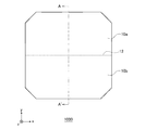
図1は、割断用太陽電池セル1000の構造を示す上面図である。図1に示すように、x軸、y軸、z軸を含む直交座標系が規定される。x軸、y軸は、割断用太陽電池セル1000の平面内において互いに直交する。z軸は、x軸およびy軸に垂直であり、割断用太陽電池セル1000の厚み方向に延びる。また、x軸、y軸、z軸のそれぞれの正の方向は、図1における矢印の方向に規定され、負の方向は、矢印と逆向きの方向に規定される。割断用太陽電池セル1000を形成する2つの主表面であって、かつx−y平面に平行な2つの主表面のうち、z軸の正方向側に配置される主平面がレーザ照射面であり、z軸の負方向側に配置される主平面がレーザ照射裏面である。以下では、z軸の正方向側を「レーザ照射面側」と呼び、z軸の負方向側を「レーザ照射裏面」と呼ぶこともある。割断用太陽電池セルおよび太陽電池セルが受光発電動作をする際、主として受光する面がz軸の正方向側であるか、負方向側であるかは任意である。
(1) Manufacturing Procedure FIG. 1 is a top view showing the structure of the
そのため、図1は、レーザ照射面側からの割断用太陽電池セル1000の構造を示す。割断用太陽電池セル1000は、例えば、正方形の四隅を角面に面取りした形状を有する。割断用太陽電池セル1000のy軸方向の中央部分には、x軸方向に延びる割断線12が配置される。割断線12は、割断用太陽電池セル1000の割断が予定される線である。ここでは、割断用太陽電池セル1000を割断線12に沿って割断することによって、第1太陽電池セル10aと第2太陽電池セル10bが形成される。第1太陽電池セル10aと第2太陽電池セル10bは太陽電池セル10と総称され、太陽電池セル10は、y軸方向よりもx軸方向に長い矩形状を有する。このような太陽電池セル10はハーフカットセルとも呼ばれる。図1に示された割断用太陽電池セル1000の形状、割断線12の配置、太陽電池セル10の形状および数は、一例であり、これに限定されない。
Therefore, FIG. 1 shows the structure of the
図2(a)−(c)は、太陽電池セル10の製造手順の概略を示し、特に、図2(a)−(b)は、固相レーザドーピングによる製造手順を示す。ここでは、図1のA−A’線に沿った割断用太陽電池セル1000の断面図が示される。図2(a)のように互いに反対を向く第1面14と第2面16を有する割断用太陽電池セル1000が用意される。第1面14は、z軸の正方向側を向いたレーザ照射面であり、p型あるいはn型である第1導電型を有する。一方、第2面16は、z軸の負方向側を向いたレーザ照射裏面であり、第1導電型とは異なる第2導電型の部分を少なくとも有する。第2導電型は、第1導電型がp型である場合にn型であり、第1導電型がn型である場合にp型である。また、第2面16は、全面的に第2導電型を有してもよく、一部に第2導電型の部分を有してもよい。割断用太陽電池セル1000の第1面14側に表面電極90が設けられ、割断用太陽電池セル1000の第2面16側に対面電極92が設けられる。割断用太陽電池セル1000の具体的な構造は(2)具体例において説明する。
2 (a)-(c) show the outline of the manufacturing procedure of the solar cell 10, and in particular, FIG. 2 (a)-(b) show the manufacturing procedure by solid-phase laser doping. Here, a cross-sectional view of the splitting
次に、割断用太陽電池セル1000におけるy軸方向の中央部分に、図1の割断線12を含むようにレーザ加工領域70が設けられる。レーザ加工領域70は、レーザを照射する予定の領域である。割断用太陽電池セル1000の第1面14上には、例えばインクジェット法あるいはディスペンス法におけるノズル72により、ドーピングプレカーサとしてドーパント源74が塗布される。ドーパント源74は、例えば、固相のドーピングペーストなどであり、レーザ加工領域70に配置される。ドーパント源74は、固相状態において、第1面14と同一の第1導電型を有する。
Next, a
次に、図2(b)のように、割断用太陽電池セル1000の第1面14側からドーパント源74にレーザ76が照射される。レーザ76の照射によって、割断用太陽電池セル1000の第1面14側部分に高ドーピング濃度領域80が形成される。高ドーピング濃度領域80は、電界効果パッシベーションにより、レーザ照射によるダメージ、あるいは出力低下を抑制する。これに続いて、レーザ76を照射することによって、割断用太陽電池セル1000が第1太陽電池セル10aと第2太陽電池セル10bとに割断されてもよい。あるいは、レーザ76を照射することによって、割断用太陽電池セル1000の第1面14上に、割断線12に沿った割断用の溝が形成されてもよい。さらに、割断用の溝に沿って、割断用太陽電池セル1000が第1太陽電池セル10aと第2太陽電池セル10bへの割断がなされてもよい。
Next, as shown in FIG. 2B, the
図2(c)は、気相レーザドーピングによる製造手順を示す。図2(a)と同一の割断用太陽電池セル1000が用意される。割断用太陽電池セル1000は、ドーピングプレカーサであるドーパントガス78の環境の中に配置される。ドーパントガス78は、ドーパント源を含んだ気相であり、例えば、p型ドーピングのためのBBr3ガス、n型ドーピングのためのPOCl3ガスである。ここでのドーパントガス78は、気相状態において、第1面14と同一の第1導電型を有する。割断用太陽電池セル1000の第1面14上に、ドーパントガス78を供給しながらレーザ76が照射される。レーザ76の照射によって、割断用太陽電池セル1000の第1面14側部分に高ドーピング濃度領域80が形成される。これに続く処理は、前述の通りであるので、ここでは説明を省略する。
FIG. 2C shows a manufacturing procedure by vapor phase laser doping. The same split
図3は、第2太陽電池セル10bの構造を示す断面図である。これは、図2(a)−(c)により割断された第2太陽電池セル10bを示す。第1面14、第2面16、表面電極90、対面電極92は、これまでと同一であるので、ここでは説明を省略する。側面18は、第1面14と第2面16との間に配置され、割断用太陽電池セル1000の厚み方向に延びる。レーザ76の照射によって、第2太陽電池セル10bの角部が削られるようにレーザ加工溝82が形成される。レーザ加工溝82の幅がレーザスクライブ幅であり、例えば、10μm以上かつ100μm以下にされる。また、レーザ加工溝82の深さは、例えば、太陽電池セル10の厚さ方向の25%以上かつ75%以下の範囲にされる。ここで、レーザ加工溝82の深さは、30%以上かつ50%以下の範囲にされることが好ましい。
FIG. 3 is a cross-sectional view showing the structure of the second
レーザ加工溝82に沿って側面18の第1面14側には、高ドーピング濃度領域80が配置される。前述のごとく、高ドーピング濃度領域80は、第1面14と同一の第1導電型を有する。これは、第2面16に含まれる第2導電型とは逆極性であることに相当する。高ドーピング濃度領域80を第1領域と呼ぶ場合、側面18の第2面16側に配置される高ドーピング濃度領域80以外の部分は、第2領域と呼ばれる。ここで、高ドーピング濃度領域80つまり前述の第1領域における第1導電型の第1不純物ピークドーピング濃度は、1019cm−3以上かつ1021cm−3以下であり、ドーピングプロファイルの半値幅は0.1μm以上かつ10μm以下である。一方、第2領域における第1不純物のドーピング濃度は、1016cm−3以下であり、第1導電型の第2不純物濃度であるといえる。このように、第1不純物濃度は第2不純物濃度よりも高い。さらに、不純物濃度は、第1面14に近づくほど高くなり、第2面16に近づくほど低くなる。また、不純物濃度は、レーザ加工溝82が形成される側面18に近づくほど高くなり、当該側面18から離れるほど低くなる。
A high
太陽電池セル10の厚み方向における第2面16からの第2領域の長さ、つまり対面距離は、太陽電池セル10の厚みの10%以上にされる。これは、高ドーピング濃度領域80によって第2面16へのリークパスが生じないようにするためである。
The length of the second region from the
(2)具体例
図4(a)−(d)は、太陽電池セル10の製造手順の具体例を示す。図4(a)−(b)は、割断用太陽電池セル1000および太陽電池セル10に、p型半導体基板200とn型半導体層240と含まれる場合を示す。具体的には、p型半導体基板200のレーザ照射面側にn型半導体層240が積層されることによって、n型半導体層240は第1面14を含み、p型半導体基板200は第2面16を含む。ここで、n型半導体層240が有する第1導電型がn型であり、p型半導体基板200が有する第2導電型がp型である。図4(a)では、このようなn型半導体層240上に、n型半導体層240と同じ第1導電型のn型ドーパント源300が配置され、n型ドーパント源300に対してレーザ76が照射される。つまり、pn接合側からレーザ76が照射される。図4(b)は、割断用太陽電池セル1000を割断した第1太陽電池セル10aと第2太陽電池セル10bを示す。第1太陽電池セル10aと第2太陽電池セル10bの側面18における第1面14側には、電界効果パッシベーションによるn++高ドープ領域320が配置される。n++高ドープ領域320は高ドーピング濃度領域80に対応する。
(2) Specific Examples FIGS. 4 (a)-(d) show specific examples of the manufacturing procedure of the solar cell 10. 4 (a)-(b) show a case where the splitting
図4(c)−(d)は、割断用太陽電池セル1000および太陽電池セル10に、n型半導体基板100とp型半導体層140と含まれる場合を示す。具体的には、n型半導体基板100のレーザ照射面側にp型半導体層140が積層されることによって、p型半導体層140は第1面14を含み、n型半導体基板100は第2面16を含む。ここで、p型半導体層140が有する第1導電型がp型であり、n型半導体基板100が有する第2導電型がn型である。図4(c)では、このようなp型半導体層140上に、p型半導体層140と同じ第1導電型のp型ドーパント源310が配置され、p型ドーパント源310に対してレーザ76が照射される。つまり、pn接合側からレーザ76が照射される。図4(d)は、割断用太陽電池セル1000を割断した第1太陽電池セル10aと第2太陽電池セル10bを示す。第1太陽電池セル10aと第2太陽電池セル10bの側面18における第1面14側には、電界効果パッシベーションによるp++高ドープ領域330が配置される。p++高ドープ領域330は高ドーピング濃度領域80に対応する。
4 (c)-(d) show a case where the splitting
図5(a)−(d)は、太陽電池セル10の製造手順の別の具体例を示す。図5(a)−(b)は、割断用太陽電池セル1000および太陽電池セル10に、p型半導体基板200とn型半導体層240と含まれる場合を示す。具体的には、p型半導体基板200のレーザ照射裏面側にn型半導体層240が積層されることによって、p型半導体基板200は第1面14を含み、n型半導体層240は第2面16を含む。ここで、p型半導体基板200が有する第1導電型がp型であり、n型半導体層240が有する第2導電型がn型である。図5(a)では、このようなp型半導体基板200上に、p型半導体基板200と同じ第1導電型のp型ドーパント源310が配置され、p型ドーパント源310に対してレーザ76が照射される。つまり、pn接合逆側からレーザ76が照射される。図5(b)は、割断用太陽電池セル1000を割断した第1太陽電池セル10aと第2太陽電池セル10bを示す。第1太陽電池セル10aと第2太陽電池セル10bの側面18における第1面14側には、電界効果パッシベーションによるp++高ドープ領域330が配置される。
5 (a)-(d) show another specific example of the manufacturing procedure of the solar cell 10. 5 (a)-(b) show a case where the splitting
図5(c)−(d)は、割断用太陽電池セル1000および太陽電池セル10に、n型半導体基板100とp型半導体層140と含まれる場合を示す。具体的には、n型半導体基板100のレーザ照射裏面側にp型半導体層140が積層されることによって、n型半導体基板100は第1面14を含み、p型半導体層140は第2面16を含む。ここで、n型半導体基板100が有する第1導電型がn型であり、p型半導体層140が有する第2導電型がp型である。図5(c)では、このようなn型半導体基板100上に、n型半導体基板100と同じ第1導電型のn型ドーパント源300が配置され、n型ドーパント源300に対してレーザ76が照射される。つまり、pn接合逆側からレーザ76が照射される。図5(d)は、割断用太陽電池セル1000を割断した第1太陽電池セル10aと第2太陽電池セル10bを示す。第1太陽電池セル10aと第2太陽電池セル10bの側面18における第1面14側には、電界効果パッシベーションによるn++高ドープ領域320が配置される。
5 (c)-(d) show a case where the splitting
図6(a)−(d)は、太陽電池セル10の製造手順のさらに別の具体例を示す。これらは、ヘテロ接合セルの構造を示す。図6(a)において、n型半導体基板100のレーザ照射面側には、真性非晶質半導体層110、p型非晶質半導体層112、p側透明導電膜層114がこの順に設けられる。真性非晶質半導体層110とp型非晶質半導体層112はp型半導体層116に含まれる。p側透明導電膜層114は、ITO(Indium Tin Oxide)等の透光性の導電性膜である。また、n型半導体基板100のレーザ照射裏面側には、真性非晶質半導体層120、n型非晶質半導体層122、n側透明導電膜層124がこの順に設けられる。真性非晶質半導体層120とn型非晶質半導体層122はn型半導体層126に含まれる。
6 (a)-(d) show still another specific example of the manufacturing procedure of the solar cell 10. These show the structure of the heterojunction cell. In FIG. 6A, the intrinsic
p側透明導電膜層114あるいはp型半導体層116は第1面14を含み、n側透明導電膜層124あるいはn型半導体層126は第2面16を含む。ここで、p型半導体層116が有する第1導電型がp型であり、n型半導体層126が有する第2導電型がn型である。図6(a)では、このようなp型半導体層116上に、p型半導体層116と同じ第1導電型のp型ドーパント源310が配置され、p型ドーパント源310に対してレーザ76が照射される。つまり、pn接合側からレーザ76が照射される。図6(b)は、割断用太陽電池セル1000を割断した第1太陽電池セル10aと第2太陽電池セル10bを示す。第1太陽電池セル10aと第2太陽電池セル10bの側面18における第1面14側には、電界効果パッシベーションによるp++高ドープ領域330が配置される。
The p-side transparent
図6(c)において、n型半導体基板100のレーザ照射面側には、真性非晶質半導体層120、n型非晶質半導体層122、n側透明導電膜層124がこの順に設けられる。真性非晶質半導体層120とn型非晶質半導体層122はn型半導体層126に含まれる。また、n型半導体基板100のレーザ照射裏面側には、真性非晶質半導体層110、p型非晶質半導体層112、p側透明導電膜層114がこの順に設けられる。真性非晶質半導体層110とp型非晶質半導体層112はp型半導体層116に含まれる。n側透明導電膜層124あるいはn型半導体層126は第1面14を含み、p側透明導電膜層114あるいはp型半導体層116は第2面16を含む。ここで、n型半導体層126が有する第1導電型がn型であり、p型半導体層116が有する第2導電型がp型である。図6(c)では、このようなn型半導体層126上に、n型半導体層126と同じ第1導電型のn型ドーパント源300が配置され、n型ドーパント源300に対してレーザ76が照射される。つまり、pn接合逆側からレーザ76が照射される。図6(d)は、割断用太陽電池セル1000を割断した第1太陽電池セル10aと第2太陽電池セル10bを示す。第1太陽電池セル10aと第2太陽電池セル10bの側面18における第1面14側には、電界効果パッシベーションによるn++高ドープ領域320が配置される。
In FIG. 6C, the intrinsic
図7(a)−(d)は、太陽電池セル10の製造手順のさらに別の具体例を示す。これはIBC(Interdigitated Back Contact)セルの構造を示す。図7(a)−(b)は、割断用太陽電池セル1000および太陽電池セル10に、p型半導体基板200とp型半導体層140とn型半導体層240と含まれる場合を示す。具体的には、p型半導体基板200のレーザ照射裏面側にp型半導体層140とn型半導体層240とが配置されることによって、p型半導体基板200は第1面14を含み、n型半導体層240は第2面16を含む。ここで、p型半導体基板200が有する第1導電型がp型であり、n型半導体層240が有する第2導電型がn型である。また、第2面16には集電極94が設けられる。図7(a)では、このようなp型半導体基板200上に、p型半導体基板200と同じ第1導電型のp型ドーパント源310が配置され、p型ドーパント源310に対してレーザ76が照射される。つまり、pn接合逆側からレーザ76が照射される。図7(b)は、割断用太陽電池セル1000を割断した第1太陽電池セル10aと第2太陽電池セル10bを示す。第1太陽電池セル10aと第2太陽電池セル10bの側面18における第1面14側には、電界効果パッシベーションによるp++高ドープ領域330が配置される。
7 (a)-(d) show still another specific example of the manufacturing procedure of the solar cell 10. This shows the structure of an IBC (Intergitated Back Contact) cell. 7 (a)-(b) show a case where the splitting
図7(c)−(d)は、割断用太陽電池セル1000および太陽電池セル10に、n型半導体基板100とp型半導体層140とn型半導体層240と含まれる場合を示す。具体的には、n型半導体基板100のレーザ照射裏面側にp型半導体層140とn型半導体層240とが配置されることによって、n型半導体基板100は第1面14を含み、p型半導体層140は第2面16を含む。ここで、n型半導体基板100が有する第1導電型がn型であり、p型半導体層140が有する第2導電型がp型である。図7(c)では、このようなn型半導体基板100上に、n型半導体基板100と同じ第1導電型のn型ドーパント源300が配置され、n型ドーパント源300に対してレーザ76が照射される。つまり、pn接合逆側からレーザ76が照射される。図7(d)は、割断用太陽電池セル1000を割断した第1太陽電池セル10aと第2太陽電池セル10bを示す。第1太陽電池セル10aと第2太陽電池セル10bの側面18における第1面14側には、電界効果パッシベーションによるn++高ドープ領域320が配置される。
7 (c)-(d) show a case where the splitting
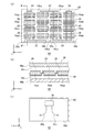
(3)太陽電池モジュールの構造
図8(a)−(c)は、太陽電池セル10を含む太陽電池モジュール50の構造を示す。図8(a)は、太陽電池モジュール50の受光面側からの平面図である。太陽電池モジュール50では、太陽電池パネル60の周囲を囲むようにフレームが取り付けられる。太陽電池パネル60は、太陽電池セル10と総称される第11太陽電池セル10aa、・・・、第44太陽電池セル10dd、ストリング間配線材22、ストリング端配線材24、セル間配線材26を含む。例えば、レーザ照射面は受光面に相当し、レーザ照射裏面は裏面に相当する。
(3) Structure of Solar Cell Module FIGS. 8 (a)-(c) show the structure of the
各太陽電池セル10は、これまで説明した割断用太陽電池セル1000の割断により生成される。また、各太陽電池セル10の受光面および裏面には、互いに平行にx軸方向に延びる複数のフィンガー電極と、複数のフィンガー電極に直交するようにy軸方向に延びる複数、例えば2本のバスバー電極とが備えられる。バスバー電極は、複数のフィンガー電極のそれぞれを接続する。また、バスバー電極およびフィンガー電極は、p側集電極およびn側集電極に相当する。
Each solar cell 10 is generated by the splitting of the splitting
複数の太陽電池セル10は、x−y平面上にマトリクス状に配列される。ここでは、一例として、x軸方向に4つの太陽電池セル10が並べられ、y軸方向に4つの太陽電池セル10が並べられる。x軸方向に並べられる太陽電池セル10の数と、y軸方向に並べられる太陽電池セル10の数は、これに限定されない。y軸方向に並んで配置される4つの太陽電池セル10は、セル間配線材26によって直列に接続され、1つの太陽電池ストリング20を形成する。例えば、第11太陽電池セル10aa、第12太陽電池セル10ab、第13太陽電池セル10ac、第14太陽電池セル10adが接続されることによって、第1太陽電池ストリング20aが形成される。他の太陽電池ストリング20、例えば、第2太陽電池ストリング20bから第4太陽電池ストリング20dも同様に形成される。その結果、4つの太陽電池ストリング20がx軸方向に平行に並べられる。
The plurality of solar cell 10s are arranged in a matrix on the xy plane. Here, as an example, four solar cells 10 are arranged in the x-axis direction, and four solar cells 10 are arranged in the y-axis direction. The number of solar cells 10 arranged in the x-axis direction and the number of solar cells 10 arranged in the y-axis direction are not limited to this. The four solar cells 10 arranged side by side in the y-axis direction are connected in series by the
太陽電池ストリング20を形成するために、セル間配線材26は、隣接した太陽電池セル10のうちの一方の受光面側のバスバー電極と、他方の裏面側のバスバー電極とを接続する。例えば、第11太陽電池セル10aaと第12太陽電池セル10abとを接続するための2つのセル間配線材26は、第11太陽電池セル10aaの受光面側のバスバー電極と第12太陽電池セル10abの裏面側のバスバー電極とを電気的に接続する。
In order to form the solar cell string 20, the
複数のストリング間配線材22のそれぞれは、x軸方向に延びて、互いに隣接する2つの太陽電池ストリング20に電気的に接続される。例えば、複数の太陽電池セル10よりもy軸の正方向に配置されるストリング間配線材22は、第2太陽電池ストリング20bにおける第21太陽電池セル10baと、第3太陽電池ストリング20cにおける第31太陽電池セル10caとを接続する。他のストリング間配線材22も同様である。その結果、複数の太陽電池ストリング20は直列に接続される。直列に接続された複数の太陽電池ストリング20の両端の太陽電池セル10、例えば、第11太陽電池セル10aaと第41太陽電池セル10daには、ストリング端配線材24が接続される。ストリング端配線材24は、図示しない端子ボックスに接続される。
Each of the plurality of
図8(b)は、太陽電池モジュール50の断面図であり、図8(a)のB−B’断面図である。太陽電池モジュール50における太陽電池パネル60は、太陽電池セル10と総称される第11太陽電池セル10aa、第12太陽電池セル10ab、第13太陽電池セル10ac、セル間配線材26、保護部材40と総称される第1保護部材40a、第2保護部材40b、封止部材42と総称される第1封止部材42a、第2封止部材42bを含む。図8(b)の上側が受光面側に相当し、下側が裏面側に相当する。
FIG. 8B is a cross-sectional view of the
第1保護部材40aは、太陽電池パネル60の受光面側に配置されており、太陽電池パネル60の表面を保護する。第1保護部材40aには、透光性および遮水性を有するガラス、透光性プラスチック等が使用され、矩形板状に形成される。ここでは、一例としてガラスが使用されるとする。第1封止部材42aは、第1保護部材40aの裏面側に積層される。第1封止部材42aは、第1保護部材40aと太陽電池セル10との間に配置されて、これらを接着する。第1封止部材42aとして、例えば、ポリオレフィン、EVA、PVB(ポリビニルブチラール)、ポリイミド等の樹脂フィルムのような熱可塑性樹脂が使用される。熱硬化性樹脂が使用されてもよい。第1封止部材42aは、透光性を有するとともに、第1保護部材40aにおけるx−y平面と略同一寸法の面を有する矩形状のシート材によって形成される。
The first
第2封止部材42bは、第1封止部材42aの裏面側に積層される。第2封止部材42bは、第1封止部材42aとの間で、複数の太陽電池セル10、セル間配線材26等を封止する。第2封止部材42bには、第1封止部材42aと同様のものを用いることができる。また、ラミネート・キュア工程における加熱によって、第2封止部材42bは第1封止部材42aと一体化されていてもよい。
The
第2保護部材40bは、第2封止部材42bの裏面側に積層される。第2保護部材40bは、バックシートとして太陽電池パネル60の裏面側を保護する。第2保護部材40bとしては、例えば、PET等の樹脂フィルムが使用される。第2保護部材40bとして、Al箔を樹脂フィルムで挟んだ構造を有する積層フィルムなどが使用されてもよい。
The second
図8(c)は、太陽電池モジュール50の裏面側からの平面図である。太陽電池モジュール50における太陽電池パネル60には、箱形形状の端子ボックス30が取り付けられる。端子ボックス30には、第1ケーブル32a、第2ケーブル32bが電気的に接続される。第1ケーブル32a、第2ケーブル32bは、太陽電池モジュール50において発電した電力を外部に出力する。
FIG. 8C is a plan view from the back surface side of the
本実施例によれば、割断用太陽電池セル1000において、第1導電型を有する第1面14上に、第1導電型のドーパント源74を配置して、ドーパント源にレーザ76を照射するので、太陽電池セル10の側面18に高ドーピング濃度領域80を形成できる。また、太陽電池セル10の側面18に高ドーピング濃度領域80が形成されるので、電界効果型パッシベーション効果により、割断による発電の出力の低下を抑制できる。また、割断用太陽電池セル1000において、第1導電型を有する第1面14上に、第1導電型のドーパントガスを供給しながらレーザ76を照射するので、太陽電池セル10の側面18に高ドーピング濃度領域80を形成できる。
According to this embodiment, in the
また、半導体層と半導体基板とが積層され、半導体層は第1面14を含み、半導体基板は第2面16を含むので、第1面14における導電型とドーパント源74の導電型とを合わせることができる。また、n型半導体層126とn型半導体基板100とp型半導体層116とが順に積層され、n型半導体層126は第1面14を含み、p型半導体層116は第2面16を含むので、第1面14における導電型とドーパント源74の導電型とを合わせることができる。
Further, since the semiconductor layer and the semiconductor substrate are laminated, the semiconductor layer includes the
また、レーザ76を照射することによって、割断用太陽電池セル1000を複数の太陽電池セル10に割断するので、複数の太陽電池セル10を製造できる。また、レーザ76を照射することによって、割断用太陽電池セル1000の第1面14上に形成した割断用の溝に沿って、割断用太陽電池セル1000を複数の太陽電池セル10に割断するので、複数の太陽電池セル10を製造できる。また、側面18において、第1面14側には第1領域が配置され、第2面16側には第2領域が配置されるとともに、第1領域における第1不純物濃度は、第2領域における第2不純物濃度よりも高いので、割断による発電の出力の低下を抑制できる。また、第2面16から第1面14への方向における第2面16からの第2領域の長さは、第2面16から第1面14への長さの10%以上であるので、リークパスの形成を防止できる。
Further, by irradiating the
本実施例の概要は、次の通りである。本開示のある態様の太陽電池セル10の製造方法は、第1導電型を有する第1面14と、第1導電型とは異なる第2導電型の部分を少なくとも有する第2面16とが反対を向いた割断用太陽電池セル1000を用意するステップと、割断用太陽電池セル1000の第1面14上に、第1導電型のドーパント源74を配置するステップと、ドーパント源74にレーザ76を照射するステップと、を備える。
The outline of this embodiment is as follows. In the method for manufacturing a solar cell 10 according to an aspect of the present disclosure, the
本開示の別の態様もまた、太陽電池セル10の製造方法である。この方法は、第1導電型を有する第1面14と、第1導電型とは異なる第2導電型の部分を少なくとも有する第2面16とが反対を向いた割断用太陽電池セル1000を用意するステップと、割断用太陽電池セル1000の第1面14上に、第1導電型のドーパントガス78を供給しながらレーザ76を照射するステップと、を備える。
Another aspect of the present disclosure is also a method of manufacturing the solar cell 10. In this method, a
割断用太陽電池セル1000では、第1導電型を有するn型半導体層240と、第2導電型を有するp型半導体基板200とが積層され、n型半導体層240は第1面14を含んでもよい。p型半導体基板200は第2面16を含む。
In the
割断用太陽電池セル1000では、第1導電型を有するn型半導体層126と、第1導電型を有するn型半導体基板100と、第2導電型を有するp型半導体層116とが順に積層され、n型半導体層126は第1面14を含んでもよい。p型半導体層116は第2面16を含む。
In the
割断用太陽電池セル1000では、第2導電型を有するp型半導体層140と、第1導電型を有するn型半導体基板100とが積層され、p型半導体層140は第2面16を含んでもよい。n型半導体基板100は第1面14を含む。
In the
割断用太陽電池セル1000では、第2導電型を有するn型半導体層126と、第2導電型のn型半導体基板100と、第1導電型を有するp型半導体層116とが順に積層され、n型半導体層126は第2面16を含んでもよい。p型半導体層116は第1面14を含む。
In the
レーザ76を照射することによって、割断用太陽電池セル1000を複数の太陽電池セル10に割断するステップとをさらに備える。
It further includes a step of dividing the
レーザ76を照射することによって、割断用太陽電池セル1000の第1面14上に、割断用の溝を形成するステップと、割断用の溝に沿って、割断用太陽電池セル1000を複数の太陽電池セル10に割断するステップとをさらに備える。
A step of forming a groove for cutting on the
本開示のさらに別の態様は、太陽電池セル10である。この太陽電池セル10は、第1導電型を有する第1面14と、第1面14とは反対を向き、かつ第1導電型とは異なる第2導電型の部分を少なくとも有する第2面16と、第1面14と第2面16との間に配置される側面18とを備える。側面18において、第1面14側には第1領域が配置され、第2面16側には第2領域が配置されるとともに、第1領域における第1導電型の第1不純物濃度は、第2領域における第1導電型の第2不純物濃度よりも高い。
Yet another aspect of the present disclosure is the solar cell 10. The solar cell 10 has a
第2面16から第1面14への方向における第2面16からの第2領域の長さは、第2面16から第1面14への長さの10%以上である。
The length of the second region from the
本開示のさらに別の態様は、太陽電池モジュール50である。この太陽電池モジュール50は、複数の太陽電池セル10を備える。複数の太陽電池セル10のそれぞれは、第1導電型を有する第1面14と、第1面14とは反対を向き、かつ第1導電型とは異なる第2導電型の部分を少なくとも有する第2面16と、第1面14と第2面16との間に配置される側面18とを備える。側面18において、第1面14側には第1領域が配置され、第2面16側には第2領域が配置されるとともに、第1領域における第1導電型の第1不純物濃度は、第2領域における第1導電型の第2不純物濃度よりも高い。
Yet another aspect of the present disclosure is the
以上、本開示について実施例をもとに説明した。この実施例は例示であり、それらの各構成要素あるいは各処理プロセスの組合せにいろいろな変形例が可能なこと、またそうした変形例も本開示の範囲にあることは当業者に理解されるところである。 The present disclosure has been described above based on examples. This embodiment is an example, and it will be understood by those skilled in the art that various modifications are possible for each of these components or combinations of each processing process, and that such modifications are also within the scope of the present disclosure. ..
10 太陽電池セル、 12 割断線、 14 第1面、 16 第2面、 18 側面、 20 太陽電池ストリング、 22 ストリング間配線材、 24 ストリング端配線材、 26 セル間配線材、 30 端子ボックス、 32 ケーブル、 40 保護部材、 42 封止部材、 50 太陽電池モジュール、 60 太陽電池パネル、 70 レーザ加工領域、 72 ノズル、 74 ドーパント源、 76 レーザ、 78 ドーパントガス、 80 高ドーピング濃度領域、 82 レーザ加工溝、 90 表面電極、 92 対面電極、 94 集電極、 100 n型半導体基板、 110 真性非晶質半導体層、 112 p型非晶質半導体層、 114 p側透明導電膜層、 116 p型半導体層、 120 真性非晶質半導体層、 122 n型非晶質半導体層、 124 n側透明導電膜層、 126 n型半導体層、 140 p型半導体層、 200 p型半導体基板、 240 n型半導体層、 300 n型ドーパント源、 310 p型ドーパント源、 320 n++高ドープ領域、 330 p++高ドープ領域、 1000 割断用太陽電池セル。 10 Solar cell, 12 Break wire, 14 1st surface, 16 2nd surface, 18 Side surface, 20 Solar cell string, 22 String-to-string wiring material, 24 String end wiring material, 26 Cell-to-cell wiring material, 30 Terminal box, 32 Cable, 40 Protective member, 42 Encapsulant member, 50 Solar cell module, 60 Solar cell panel, 70 Laser processing area, 72 nozzle, 74 Dopant source, 76 Laser, 78 Dopant gas, 80 High doping concentration area, 82 Laser processing groove , 90 surface electrode, 92 face-to-face electrode, 94 collecting electrode, 100 n-type semiconductor substrate, 110 intrinsic amorphous semiconductor layer, 112 p-type amorphous semiconductor layer, 114 p-side transparent conductive film layer, 116 p-type semiconductor layer, 120 Intrinsic amorphous semiconductor layer, 122 n-type amorphous semiconductor layer, 124 n-side transparent conductive film layer, 126 n-type semiconductor layer, 140 p-type semiconductor layer, 200 p-type semiconductor substrate, 240 n-type semiconductor layer, 300 n-type dopant source, 310 p-type dopant source, 320 n ++ high-doped region, 330 p ++ high-doped region, 1000 splitting solar cell.
Claims (11)
前記割断用太陽電池セルの前記第1面上に、前記第1導電型のドーパント源を配置するステップと、
前記ドーパント源にレーザを照射するステップと、
を備える太陽電池セルの製造方法。 A step of preparing a solar cell for splitting in which the first surface having the first conductive type and the second surface having at least a second conductive type portion different from the first conductive type are opposite to each other.
A step of arranging the first conductive type dopant source on the first surface of the cutting solar cell, and
The step of irradiating the dopant source with a laser and
A method of manufacturing a solar cell comprising.
前記割断用太陽電池セルの前記第1面上に、前記第1導電型のドーパントガスを供給しながらレーザを照射するステップと、
を備える太陽電池セルの製造方法。 A step of preparing a solar cell for splitting in which the first surface having the first conductive type and the second surface having at least a second conductive type portion different from the first conductive type are opposite to each other.
A step of irradiating a laser while supplying the first conductive type dopant gas onto the first surface of the splitting solar cell.
A method of manufacturing a solar cell comprising.
前記半導体層は前記第1面を含み、
前記半導体基板は前記第2面を含む、
請求項1または2に記載の太陽電池セルの製造方法。 In the solar cell for cutting, the semiconductor layer having the first conductive type and the semiconductor substrate having the second conductive type are laminated.
The semiconductor layer includes the first surface.
The semiconductor substrate includes the second surface.
The method for manufacturing a solar cell according to claim 1 or 2.
前記第1半導体層は前記第1面を含み、
前記第2半導体層は前記第2面を含む、
請求項1または2に記載の太陽電池セルの製造方法。 In the solar cell for cutting, the first semiconductor layer having the first conductive type, the semiconductor substrate having the first conductive type, and the second semiconductor layer having the second conductive type are laminated in this order.
The first semiconductor layer includes the first surface.
The second semiconductor layer includes the second surface.
The method for manufacturing a solar cell according to claim 1 or 2.
前記半導体層は前記第2面を含み、
前記半導体基板は前記第1面を含む、
請求項1または2に記載の太陽電池セルの製造方法。 In the solar cell for cutting, the semiconductor layer having the second conductive type and the semiconductor substrate having the first conductive type are laminated.
The semiconductor layer includes the second surface.
The semiconductor substrate includes the first surface.
The method for manufacturing a solar cell according to claim 1 or 2.
前記第1半導体層は前記第2面を含み、
前記第2半導体層は前記第1面を含む、
請求項1または2に記載の太陽電池セルの製造方法。 In the solar cell for cutting, the first semiconductor layer having the second conductive type, the second conductive type semiconductor substrate, and the second semiconductor layer having the first conductive type are laminated in this order.
The first semiconductor layer includes the second surface.
The second semiconductor layer includes the first surface.
The method for manufacturing a solar cell according to claim 1 or 2.
請求項1から6のいずれか1項に記載の太陽電池セルの製造方法。 Further comprising a step of dividing the splitting solar cell into a plurality of solar cells by irradiating the laser.
The method for manufacturing a solar cell according to any one of claims 1 to 6.
前記割断用の溝に沿って、前記割断用太陽電池セルを複数の太陽電池セルに割断するステップとをさらに備える、
請求項1から6のいずれか1項に記載の太陽電池セルの製造方法。 A step of forming a groove for cutting on the first surface of the solar cell for cutting by irradiating the laser.
A step of dividing the solar cell for division into a plurality of solar cells along the groove for division is further provided.
The method for manufacturing a solar cell according to any one of claims 1 to 6.
前記第1面とは反対を向き、かつ前記第1導電型とは異なる第2導電型の部分を少なくとも有する第2面と、
前記第1面と前記第2面との間に配置される側面とを備え、
前記側面において、前記第1面側には第1領域が配置され、前記第2面側には第2領域が配置されるとともに、前記第1領域における前記第1導電型の第1不純物濃度は、前記第2領域における前記第1導電型の第2不純物濃度よりも高い、
太陽電池セル。 The first surface having the first conductive type and
A second surface that faces the opposite side of the first surface and has at least a second conductive type portion that is different from the first conductive type.
A side surface arranged between the first surface and the second surface is provided.
On the side surface, a first region is arranged on the first surface side, a second region is arranged on the second surface side, and the concentration of the first impurity of the first conductive type in the first region is , Higher than the second impurity concentration of the first conductive type in the second region.
Solar cell.
請求項9に記載の太陽電池セル。 The length of the second region from the second surface in the direction from the second surface to the first surface is 10% or more of the length from the second surface to the first surface.
The solar cell according to claim 9.
前記複数の太陽電池セルのそれぞれは、
第1導電型を有する第1面と、
前記第1面とは反対を向き、かつ前記第1導電型とは異なる第2導電型の部分を少なくとも有する第2面と、
前記第1面と前記第2面との間に配置される側面とを備え、
前記側面において、前記第1面側には第1領域が配置され、前記第2面側には第2領域が配置されるとともに、前記第1領域における前記第1導電型の第1不純物濃度は、前記第2領域における前記第1導電型の第2不純物濃度よりも高い、
太陽電池モジュール。 Equipped with multiple solar cells
Each of the plurality of solar cells
The first surface having the first conductive type and
A second surface that faces the opposite side of the first surface and has at least a second conductive type portion that is different from the first conductive type.
A side surface arranged between the first surface and the second surface is provided.
On the side surface, a first region is arranged on the first surface side, a second region is arranged on the second surface side, and the concentration of the first impurity of the first conductive type in the first region is , Higher than the second impurity concentration of the first conductive type in the second region.
Solar cell module.
Priority Applications (3)
| Application Number | Priority Date | Filing Date | Title |
|---|---|---|---|
| JP2019061113A JP2020161701A (en) | 2019-03-27 | 2019-03-27 | Manufacturing method of solar cell, solar cell, and solar cell module |
| US16/816,128 US20200313030A1 (en) | 2019-03-27 | 2020-03-11 | Method of manufacturing solar cell for manufacturing solar cell from splittable solar cell that can be split, solar cell, and solar cell module |
| CN202010227237.9A CN111834490A (en) | 2019-03-27 | 2020-03-27 | Method for manufacturing solar cell, and solar cell module |
Applications Claiming Priority (1)
| Application Number | Priority Date | Filing Date | Title |
|---|---|---|---|
| JP2019061113A JP2020161701A (en) | 2019-03-27 | 2019-03-27 | Manufacturing method of solar cell, solar cell, and solar cell module |
Publications (1)
| Publication Number | Publication Date |
|---|---|
| JP2020161701A true JP2020161701A (en) | 2020-10-01 |
Family
ID=72604920
Family Applications (1)
| Application Number | Title | Priority Date | Filing Date |
|---|---|---|---|
| JP2019061113A Pending JP2020161701A (en) | 2019-03-27 | 2019-03-27 | Manufacturing method of solar cell, solar cell, and solar cell module |
Country Status (3)
| Country | Link |
|---|---|
| US (1) | US20200313030A1 (en) |
| JP (1) | JP2020161701A (en) |
| CN (1) | CN111834490A (en) |
-
2019
- 2019-03-27 JP JP2019061113A patent/JP2020161701A/en active Pending
-
2020
- 2020-03-11 US US16/816,128 patent/US20200313030A1/en not_active Abandoned
- 2020-03-27 CN CN202010227237.9A patent/CN111834490A/en not_active Withdrawn
Also Published As
| Publication number | Publication date |
|---|---|
| US20200313030A1 (en) | 2020-10-01 |
| CN111834490A (en) | 2020-10-27 |
Similar Documents
| Publication | Publication Date | Title |
|---|---|---|
| JP6586080B2 (en) | Solar cell module and manufacturing method thereof | |
| KR101130197B1 (en) | Solar cell module and manufacturing method thereof | |
| EP2043163B1 (en) | Method of manufacturing solar cell module and solar cell module thus manufactured | |
| JP5171001B2 (en) | Method for manufacturing solar cell module, solar cell and solar cell module | |
| JP7278831B2 (en) | SOLAR BATTERY CELL MANUFACTURING METHOD AND CUTTING SOLAR BATTERY CELL | |
| KR20180014172A (en) | Metallization and stringing methods for back-contacting solar cells | |
| US20090078301A1 (en) | Solar cell module | |
| KR20110034182A (en) | Solar cell module and manufacturing method thereof | |
| US20130098447A1 (en) | Method for manufacturing solar battery module and solar battery module manufactured by the manufacturing method | |
| US20140157580A1 (en) | Solar module manufacturing method | |
| US11515436B2 (en) | Photovoltaic device and photovoltaic unit | |
| JPWO2018051658A1 (en) | Solar cell module | |
| JP2013143529A (en) | Solar cell module | |
| JP2018046112A (en) | Solar cell module | |
| JP2017174986A (en) | Solar battery cell and solar battery module | |
| JP2020161701A (en) | Manufacturing method of solar cell, solar cell, and solar cell module | |
| JPWO2019087590A1 (en) | Double-sided electrode type solar cell and solar cell module | |
| JP2018056490A (en) | Solar cell module and solar cell | |
| JP2017152604A (en) | Solar cell element and solar cell module | |
| JP2011249736A (en) | Solar cell module manufacturing method | |
| WO2014103513A1 (en) | Solar cell module and solar cell module manufacturing method | |
| WO2018116782A1 (en) | Solar cell and method for producing solar cell | |
| WO2013031298A1 (en) | Solar cell module and method for producing same | |
| JP2020161545A (en) | Solar cell for splitting and solar cell | |
| JP2018074125A (en) | Solar battery cell, solar battery module, and method for manufacturing solar battery cell |