JP2020142014A - Electrode and biological sensor - Google Patents
Electrode and biological sensor Download PDFInfo
- Publication number
- JP2020142014A JP2020142014A JP2019042985A JP2019042985A JP2020142014A JP 2020142014 A JP2020142014 A JP 2020142014A JP 2019042985 A JP2019042985 A JP 2019042985A JP 2019042985 A JP2019042985 A JP 2019042985A JP 2020142014 A JP2020142014 A JP 2020142014A
- Authority
- JP
- Japan
- Prior art keywords
- electrode
- plasticizer
- mass
- content
- sensitive adhesive
- Prior art date
- Legal status (The legal status is an assumption and is not a legal conclusion. Google has not performed a legal analysis and makes no representation as to the accuracy of the status listed.)
- Pending
Links
- 239000004014 plasticizer Substances 0.000 claims abstract description 65
- 229920001940 conductive polymer Polymers 0.000 claims abstract description 40
- 239000002344 surface layer Substances 0.000 claims abstract description 33
- 229920005989 resin Polymers 0.000 claims abstract description 32
- 239000011347 resin Substances 0.000 claims abstract description 32
- 239000011230 binding agent Substances 0.000 claims abstract description 22
- 239000010410 layer Substances 0.000 claims description 102
- 239000004820 Pressure-sensitive adhesive Substances 0.000 claims description 66
- PEDCQBHIVMGVHV-UHFFFAOYSA-N glycerol group Chemical group OCC(O)CO PEDCQBHIVMGVHV-UHFFFAOYSA-N 0.000 claims description 14
- 235000011187 glycerol Nutrition 0.000 claims description 7
- 230000000149 penetrating effect Effects 0.000 claims description 3
- 239000000203 mixture Substances 0.000 description 79
- 239000000463 material Substances 0.000 description 52
- 239000000523 sample Substances 0.000 description 50
- 239000000758 substrate Substances 0.000 description 39
- 239000003431 cross linking reagent Substances 0.000 description 28
- 239000007864 aqueous solution Substances 0.000 description 23
- 239000004372 Polyvinyl alcohol Substances 0.000 description 18
- -1 dimethylsiloxane Chemical class 0.000 description 18
- 229920002451 polyvinyl alcohol Polymers 0.000 description 18
- 238000000034 method Methods 0.000 description 14
- 229920000642 polymer Polymers 0.000 description 14
- 238000012360 testing method Methods 0.000 description 14
- 239000002904 solvent Substances 0.000 description 13
- ZWEHNKRNPOVVGH-UHFFFAOYSA-N 2-Butanone Chemical compound CCC(C)=O ZWEHNKRNPOVVGH-UHFFFAOYSA-N 0.000 description 12
- ZMXDDKWLCZADIW-UHFFFAOYSA-N N,N-Dimethylformamide Chemical compound CN(C)C=O ZMXDDKWLCZADIW-UHFFFAOYSA-N 0.000 description 12
- 238000005259 measurement Methods 0.000 description 12
- 238000011156 evaluation Methods 0.000 description 9
- 229920000058 polyacrylate Polymers 0.000 description 9
- 239000012790 adhesive layer Substances 0.000 description 8
- 150000001875 compounds Chemical class 0.000 description 8
- 229920002799 BoPET Polymers 0.000 description 7
- OKKJLVBELUTLKV-UHFFFAOYSA-N Methanol Chemical compound OC OKKJLVBELUTLKV-UHFFFAOYSA-N 0.000 description 7
- 238000001069 Raman spectroscopy Methods 0.000 description 7
- NIXOWILDQLNWCW-UHFFFAOYSA-N acrylic acid group Chemical group C(C=C)(=O)O NIXOWILDQLNWCW-UHFFFAOYSA-N 0.000 description 7
- 238000010438 heat treatment Methods 0.000 description 7
- 125000002887 hydroxy group Chemical group [H]O* 0.000 description 7
- 239000004094 surface-active agent Substances 0.000 description 7
- 150000003755 zirconium compounds Chemical class 0.000 description 7
- XEKOWRVHYACXOJ-UHFFFAOYSA-N Ethyl acetate Chemical compound CCOC(C)=O XEKOWRVHYACXOJ-UHFFFAOYSA-N 0.000 description 6
- 102000011782 Keratins Human genes 0.000 description 6
- 108010076876 Keratins Proteins 0.000 description 6
- 239000003125 aqueous solvent Substances 0.000 description 6
- 150000001733 carboxylic acid esters Chemical class 0.000 description 6
- 238000000576 coating method Methods 0.000 description 6
- 230000000052 comparative effect Effects 0.000 description 6
- IAZDPXIOMUYVGZ-UHFFFAOYSA-N Dimethylsulphoxide Chemical compound CS(C)=O IAZDPXIOMUYVGZ-UHFFFAOYSA-N 0.000 description 5
- LFQSCWFLJHTTHZ-UHFFFAOYSA-N Ethanol Chemical compound CCO LFQSCWFLJHTTHZ-UHFFFAOYSA-N 0.000 description 5
- 238000005033 Fourier transform infrared spectroscopy Methods 0.000 description 5
- 239000004642 Polyimide Substances 0.000 description 5
- 239000000853 adhesive Substances 0.000 description 5
- 230000001070 adhesive effect Effects 0.000 description 5
- 229920000249 biocompatible polymer Polymers 0.000 description 5
- 238000006243 chemical reaction Methods 0.000 description 5
- 239000011248 coating agent Substances 0.000 description 5
- 238000004519 manufacturing process Methods 0.000 description 5
- 229910052751 metal Inorganic materials 0.000 description 5
- 239000002184 metal Substances 0.000 description 5
- 229920001721 polyimide Polymers 0.000 description 5
- CSCPPACGZOOCGX-UHFFFAOYSA-N Acetone Chemical compound CC(C)=O CSCPPACGZOOCGX-UHFFFAOYSA-N 0.000 description 4
- KFZMGEQAYNKOFK-UHFFFAOYSA-N Isopropanol Chemical compound CC(C)O KFZMGEQAYNKOFK-UHFFFAOYSA-N 0.000 description 4
- 230000007423 decrease Effects 0.000 description 4
- 230000006870 function Effects 0.000 description 4
- 239000012948 isocyanate Substances 0.000 description 4
- 239000003960 organic solvent Substances 0.000 description 4
- 229920001296 polysiloxane Polymers 0.000 description 4
- 229920003169 water-soluble polymer Polymers 0.000 description 4
- RYGMFSIKBFXOCR-UHFFFAOYSA-N Copper Chemical compound [Cu] RYGMFSIKBFXOCR-UHFFFAOYSA-N 0.000 description 3
- LYCAIKOWRPUZTN-UHFFFAOYSA-N Ethylene glycol Chemical compound OCCO LYCAIKOWRPUZTN-UHFFFAOYSA-N 0.000 description 3
- CERQOIWHTDAKMF-UHFFFAOYSA-N Methacrylic acid Chemical compound CC(=C)C(O)=O CERQOIWHTDAKMF-UHFFFAOYSA-N 0.000 description 3
- DNIAPMSPPWPWGF-UHFFFAOYSA-N Propylene glycol Chemical compound CC(O)CO DNIAPMSPPWPWGF-UHFFFAOYSA-N 0.000 description 3
- 239000003795 chemical substances by application Substances 0.000 description 3
- 238000004891 communication Methods 0.000 description 3
- 229910052802 copper Inorganic materials 0.000 description 3
- 239000010949 copper Substances 0.000 description 3
- 239000000178 monomer Substances 0.000 description 3
- 230000035699 permeability Effects 0.000 description 3
- 229920000139 polyethylene terephthalate Polymers 0.000 description 3
- 239000005020 polyethylene terephthalate Substances 0.000 description 3
- 230000009257 reactivity Effects 0.000 description 3
- XLYOFNOQVPJJNP-UHFFFAOYSA-N water Substances O XLYOFNOQVPJJNP-UHFFFAOYSA-N 0.000 description 3
- ARXJGSRGQADJSQ-UHFFFAOYSA-N 1-methoxypropan-2-ol Chemical compound COCC(C)O ARXJGSRGQADJSQ-UHFFFAOYSA-N 0.000 description 2
- VMAWODUEPLAHOE-UHFFFAOYSA-N 2,4,6,8-tetrakis(ethenyl)-2,4,6,8-tetramethyl-1,3,5,7,2,4,6,8-tetraoxatetrasilocane Chemical compound C=C[Si]1(C)O[Si](C)(C=C)O[Si](C)(C=C)O[Si](C)(C=C)O1 VMAWODUEPLAHOE-UHFFFAOYSA-N 0.000 description 2
- SECXISVLQFMRJM-UHFFFAOYSA-N N-Methylpyrrolidone Chemical compound CN1CCCC1=O SECXISVLQFMRJM-UHFFFAOYSA-N 0.000 description 2
- PXHVJJICTQNCMI-UHFFFAOYSA-N Nickel Chemical compound [Ni] PXHVJJICTQNCMI-UHFFFAOYSA-N 0.000 description 2
- 239000004952 Polyamide Substances 0.000 description 2
- 239000004698 Polyethylene Substances 0.000 description 2
- 239000004743 Polypropylene Substances 0.000 description 2
- 238000000862 absorption spectrum Methods 0.000 description 2
- 230000036982 action potential Effects 0.000 description 2
- 150000001298 alcohols Chemical class 0.000 description 2
- 150000001408 amides Chemical class 0.000 description 2
- 239000003963 antioxidant agent Substances 0.000 description 2
- 230000003078 antioxidant effect Effects 0.000 description 2
- 239000011162 core material Substances 0.000 description 2
- 238000004132 cross linking Methods 0.000 description 2
- 230000002950 deficient Effects 0.000 description 2
- SWXVUIWOUIDPGS-UHFFFAOYSA-N diacetone alcohol Chemical compound CC(=O)CC(C)(C)O SWXVUIWOUIDPGS-UHFFFAOYSA-N 0.000 description 2
- 238000010586 diagram Methods 0.000 description 2
- 238000001035 drying Methods 0.000 description 2
- 150000002148 esters Chemical class 0.000 description 2
- 150000002170 ethers Chemical class 0.000 description 2
- 238000004299 exfoliation Methods 0.000 description 2
- LEQAOMBKQFMDFZ-UHFFFAOYSA-N glyoxal Chemical compound O=CC=O LEQAOMBKQFMDFZ-UHFFFAOYSA-N 0.000 description 2
- 239000012212 insulator Substances 0.000 description 2
- 150000002576 ketones Chemical class 0.000 description 2
- 238000012986 modification Methods 0.000 description 2
- 230000004048 modification Effects 0.000 description 2
- 230000002107 myocardial effect Effects 0.000 description 2
- 210000004165 myocardium Anatomy 0.000 description 2
- 230000002093 peripheral effect Effects 0.000 description 2
- 229920003023 plastic Polymers 0.000 description 2
- 239000004033 plastic Substances 0.000 description 2
- 229920002647 polyamide Polymers 0.000 description 2
- 229920000573 polyethylene Polymers 0.000 description 2
- 229920001228 polyisocyanate Polymers 0.000 description 2
- 239000005056 polyisocyanate Substances 0.000 description 2
- 229920001155 polypropylene Polymers 0.000 description 2
- 229920000123 polythiophene Polymers 0.000 description 2
- 238000002360 preparation method Methods 0.000 description 2
- 238000012545 processing Methods 0.000 description 2
- BDERNNFJNOPAEC-UHFFFAOYSA-N propan-1-ol Chemical compound CCCO BDERNNFJNOPAEC-UHFFFAOYSA-N 0.000 description 2
- 238000009864 tensile test Methods 0.000 description 2
- PQUXFUBNSYCQAL-UHFFFAOYSA-N 1-(2,3-difluorophenyl)ethanone Chemical compound CC(=O)C1=CC=CC(F)=C1F PQUXFUBNSYCQAL-UHFFFAOYSA-N 0.000 description 1
- GKWLILHTTGWKLQ-UHFFFAOYSA-N 2,3-dihydrothieno[3,4-b][1,4]dioxine Chemical compound O1CCOC2=CSC=C21 GKWLILHTTGWKLQ-UHFFFAOYSA-N 0.000 description 1
- VZSRBBMJRBPUNF-UHFFFAOYSA-N 2-(2,3-dihydro-1H-inden-2-ylamino)-N-[3-oxo-3-(2,4,6,7-tetrahydrotriazolo[4,5-c]pyridin-5-yl)propyl]pyrimidine-5-carboxamide Chemical compound C1C(CC2=CC=CC=C12)NC1=NC=C(C=N1)C(=O)NCCC(N1CC2=C(CC1)NN=N2)=O VZSRBBMJRBPUNF-UHFFFAOYSA-N 0.000 description 1
- SMZOUWXMTYCWNB-UHFFFAOYSA-N 2-(2-methoxy-5-methylphenyl)ethanamine Chemical compound COC1=CC=C(C)C=C1CCN SMZOUWXMTYCWNB-UHFFFAOYSA-N 0.000 description 1
- HFCUBKYHMMPGBY-UHFFFAOYSA-N 2-methoxyethyl prop-2-enoate Chemical compound COCCOC(=O)C=C HFCUBKYHMMPGBY-UHFFFAOYSA-N 0.000 description 1
- 125000003504 2-oxazolinyl group Chemical class O1C(=NCC1)* 0.000 description 1
- CUXGDKOCSSIRKK-UHFFFAOYSA-N 7-methyloctyl prop-2-enoate Chemical compound CC(C)CCCCCCOC(=O)C=C CUXGDKOCSSIRKK-UHFFFAOYSA-N 0.000 description 1
- NIXOWILDQLNWCW-UHFFFAOYSA-M Acrylate Chemical compound [O-]C(=O)C=C NIXOWILDQLNWCW-UHFFFAOYSA-M 0.000 description 1
- 239000004925 Acrylic resin Substances 0.000 description 1
- 229920000178 Acrylic resin Polymers 0.000 description 1
- 229920000936 Agarose Polymers 0.000 description 1
- 241000283690 Bos taurus Species 0.000 description 1
- 241000282472 Canis lupus familiaris Species 0.000 description 1
- FBPFZTCFMRRESA-FSIIMWSLSA-N D-Glucitol Natural products OC[C@H](O)[C@H](O)[C@@H](O)[C@H](O)CO FBPFZTCFMRRESA-FSIIMWSLSA-N 0.000 description 1
- FBPFZTCFMRRESA-JGWLITMVSA-N D-glucitol Chemical compound OC[C@H](O)[C@@H](O)[C@H](O)[C@H](O)CO FBPFZTCFMRRESA-JGWLITMVSA-N 0.000 description 1
- ZNZYKNKBJPZETN-WELNAUFTSA-N Dialdehyde 11678 Chemical compound N1C2=CC=CC=C2C2=C1[C@H](C[C@H](/C(=C/O)C(=O)OC)[C@@H](C=C)C=O)NCC2 ZNZYKNKBJPZETN-WELNAUFTSA-N 0.000 description 1
- 239000004593 Epoxy Chemical class 0.000 description 1
- 241000283086 Equidae Species 0.000 description 1
- JOYRKODLDBILNP-UHFFFAOYSA-N Ethyl urethane Chemical compound CCOC(N)=O JOYRKODLDBILNP-UHFFFAOYSA-N 0.000 description 1
- 241000282326 Felis catus Species 0.000 description 1
- 241000287828 Gallus gallus Species 0.000 description 1
- HBBGRARXTFLTSG-UHFFFAOYSA-N Lithium ion Chemical compound [Li+] HBBGRARXTFLTSG-UHFFFAOYSA-N 0.000 description 1
- 241001465754 Metazoa Species 0.000 description 1
- FXHOOIRPVKKKFG-UHFFFAOYSA-N N,N-Dimethylacetamide Chemical compound CN(C)C(C)=O FXHOOIRPVKKKFG-UHFFFAOYSA-N 0.000 description 1
- 238000003841 Raman measurement Methods 0.000 description 1
- 239000004902 Softening Agent Substances 0.000 description 1
- 241000282887 Suidae Species 0.000 description 1
- BZHJMEDXRYGGRV-UHFFFAOYSA-N Vinyl chloride Chemical compound ClC=C BZHJMEDXRYGGRV-UHFFFAOYSA-N 0.000 description 1
- 239000002253 acid Substances 0.000 description 1
- 229940048053 acrylate Drugs 0.000 description 1
- 239000000654 additive Substances 0.000 description 1
- 238000007754 air knife coating Methods 0.000 description 1
- 125000003545 alkoxy group Chemical group 0.000 description 1
- 239000000956 alloy Substances 0.000 description 1
- 229910045601 alloy Inorganic materials 0.000 description 1
- HSFWRNGVRCDJHI-UHFFFAOYSA-N alpha-acetylene Natural products C#C HSFWRNGVRCDJHI-UHFFFAOYSA-N 0.000 description 1
- 229910052782 aluminium Inorganic materials 0.000 description 1
- XAGFODPZIPBFFR-UHFFFAOYSA-N aluminium Chemical compound [Al] XAGFODPZIPBFFR-UHFFFAOYSA-N 0.000 description 1
- 210000003423 ankle Anatomy 0.000 description 1
- 206010003119 arrhythmia Diseases 0.000 description 1
- 230000006793 arrhythmia Effects 0.000 description 1
- 150000001541 aziridines Chemical class 0.000 description 1
- 238000005452 bending Methods 0.000 description 1
- KGBXLFKZBHKPEV-UHFFFAOYSA-N boric acid Chemical compound OB(O)O KGBXLFKZBHKPEV-UHFFFAOYSA-N 0.000 description 1
- 239000004327 boric acid Substances 0.000 description 1
- 239000003990 capacitor Substances 0.000 description 1
- 150000001720 carbohydrates Chemical class 0.000 description 1
- 239000000919 ceramic Substances 0.000 description 1
- 239000013522 chelant Substances 0.000 description 1
- 235000013330 chicken meat Nutrition 0.000 description 1
- 238000004140 cleaning Methods 0.000 description 1
- 239000003086 colorant Substances 0.000 description 1
- 230000008602 contraction Effects 0.000 description 1
- 229920001577 copolymer Polymers 0.000 description 1
- 238000007598 dipping method Methods 0.000 description 1
- 238000005401 electroluminescence Methods 0.000 description 1
- 239000000835 fiber Substances 0.000 description 1
- 239000000945 filler Substances 0.000 description 1
- 238000001914 filtration Methods 0.000 description 1
- 239000011888 foil Substances 0.000 description 1
- 235000010855 food raising agent Nutrition 0.000 description 1
- 210000001061 forehead Anatomy 0.000 description 1
- 239000011521 glass Substances 0.000 description 1
- 239000003365 glass fiber Substances 0.000 description 1
- 125000003976 glyceryl group Chemical group [H]C([*])([H])C(O[H])([H])C(O[H])([H])[H] 0.000 description 1
- 229940015043 glyoxal Drugs 0.000 description 1
- PCHJSUWPFVWCPO-UHFFFAOYSA-N gold Chemical compound [Au] PCHJSUWPFVWCPO-UHFFFAOYSA-N 0.000 description 1
- 229910052737 gold Inorganic materials 0.000 description 1
- 239000010931 gold Substances 0.000 description 1
- 238000007756 gravure coating Methods 0.000 description 1
- 229920001477 hydrophilic polymer Polymers 0.000 description 1
- 230000010354 integration Effects 0.000 description 1
- 230000001678 irradiating effect Effects 0.000 description 1
- 150000002513 isocyanates Chemical class 0.000 description 1
- 229910001416 lithium ion Inorganic materials 0.000 description 1
- 239000011159 matrix material Substances 0.000 description 1
- 150000007974 melamines Chemical class 0.000 description 1
- 238000002156 mixing Methods 0.000 description 1
- 238000000465 moulding Methods 0.000 description 1
- 210000003205 muscle Anatomy 0.000 description 1
- 208000031225 myocardial ischemia Diseases 0.000 description 1
- OMNKZBIFPJNNIO-UHFFFAOYSA-N n-(2-methyl-4-oxopentan-2-yl)prop-2-enamide Chemical compound CC(=O)CC(C)(C)NC(=O)C=C OMNKZBIFPJNNIO-UHFFFAOYSA-N 0.000 description 1
- 229910052759 nickel Inorganic materials 0.000 description 1
- 230000000474 nursing effect Effects 0.000 description 1
- 229920000553 poly(phenylenevinylene) Polymers 0.000 description 1
- 229920000172 poly(styrenesulfonic acid) Polymers 0.000 description 1
- 229920001197 polyacetylene Polymers 0.000 description 1
- 229920000767 polyaniline Polymers 0.000 description 1
- 229920001225 polyester resin Polymers 0.000 description 1
- 239000004645 polyester resin Substances 0.000 description 1
- 229920000307 polymer substrate Polymers 0.000 description 1
- 230000000379 polymerizing effect Effects 0.000 description 1
- 229920005862 polyol Polymers 0.000 description 1
- 229920000128 polypyrrole Polymers 0.000 description 1
- 229920005990 polystyrene resin Polymers 0.000 description 1
- 229940005642 polystyrene sulfonic acid Drugs 0.000 description 1
- 229920005749 polyurethane resin Polymers 0.000 description 1
- 238000001556 precipitation Methods 0.000 description 1
- 238000003825 pressing Methods 0.000 description 1
- 230000008569 process Effects 0.000 description 1
- 230000001681 protective effect Effects 0.000 description 1
- 210000004761 scalp Anatomy 0.000 description 1
- 230000035939 shock Effects 0.000 description 1
- 229920002050 silicone resin Polymers 0.000 description 1
- 229920002379 silicone rubber Polymers 0.000 description 1
- 239000004945 silicone rubber Substances 0.000 description 1
- 210000003491 skin Anatomy 0.000 description 1
- 229940047670 sodium acrylate Drugs 0.000 description 1
- 229910000679 solder Inorganic materials 0.000 description 1
- 239000000600 sorbitol Substances 0.000 description 1
- 238000004528 spin coating Methods 0.000 description 1
- 239000003381 stabilizer Substances 0.000 description 1
- 238000003860 storage Methods 0.000 description 1
- 239000000126 substance Substances 0.000 description 1
- BDHFUVZGWQCTTF-UHFFFAOYSA-M sulfonate Chemical compound [O-]S(=O)=O BDHFUVZGWQCTTF-UHFFFAOYSA-M 0.000 description 1
- 229920005992 thermoplastic resin Polymers 0.000 description 1
- 239000002562 thickening agent Substances 0.000 description 1
- 150000003608 titanium Chemical class 0.000 description 1
- 150000003609 titanium compounds Chemical class 0.000 description 1
- 150000003672 ureas Chemical class 0.000 description 1
- 229920003176 water-insoluble polymer Polymers 0.000 description 1
- 210000000707 wrist Anatomy 0.000 description 1
- 150000003754 zirconium Chemical class 0.000 description 1
Images


Classifications
-
- A—HUMAN NECESSITIES
- A61—MEDICAL OR VETERINARY SCIENCE; HYGIENE
- A61B—DIAGNOSIS; SURGERY; IDENTIFICATION
- A61B5/00—Measuring for diagnostic purposes; Identification of persons
- A61B5/24—Detecting, measuring or recording bioelectric or biomagnetic signals of the body or parts thereof
- A61B5/25—Bioelectric electrodes therefor
- A61B5/263—Bioelectric electrodes therefor characterised by the electrode materials
- A61B5/268—Bioelectric electrodes therefor characterised by the electrode materials containing conductive polymers, e.g. PEDOT:PSS polymers
-
- A—HUMAN NECESSITIES
- A61—MEDICAL OR VETERINARY SCIENCE; HYGIENE
- A61B—DIAGNOSIS; SURGERY; IDENTIFICATION
- A61B5/00—Measuring for diagnostic purposes; Identification of persons
- A61B5/24—Detecting, measuring or recording bioelectric or biomagnetic signals of the body or parts thereof
- A61B5/25—Bioelectric electrodes therefor
- A61B5/251—Means for maintaining electrode contact with the body
- A61B5/257—Means for maintaining electrode contact with the body using adhesive means, e.g. adhesive pads or tapes
- A61B5/259—Means for maintaining electrode contact with the body using adhesive means, e.g. adhesive pads or tapes using conductive adhesive means, e.g. gels
-
- A—HUMAN NECESSITIES
- A61—MEDICAL OR VETERINARY SCIENCE; HYGIENE
- A61B—DIAGNOSIS; SURGERY; IDENTIFICATION
- A61B5/00—Measuring for diagnostic purposes; Identification of persons
- A61B5/68—Arrangements of detecting, measuring or recording means, e.g. sensors, in relation to patient
- A61B5/6801—Arrangements of detecting, measuring or recording means, e.g. sensors, in relation to patient specially adapted to be attached to or worn on the body surface
- A61B5/683—Means for maintaining contact with the body
- A61B5/6832—Means for maintaining contact with the body using adhesives
- A61B5/6833—Adhesive patches
-
- A—HUMAN NECESSITIES
- A61—MEDICAL OR VETERINARY SCIENCE; HYGIENE
- A61B—DIAGNOSIS; SURGERY; IDENTIFICATION
- A61B2562/00—Details of sensors; Constructional details of sensor housings or probes; Accessories for sensors
- A61B2562/12—Manufacturing methods specially adapted for producing sensors for in-vivo measurements
- A61B2562/125—Manufacturing methods specially adapted for producing sensors for in-vivo measurements characterised by the manufacture of electrodes
Abstract
Description
本発明は、電極及び生体センサに関する。 The present invention relates to electrodes and biosensors.
病院や診療所等の医療機関、介護施設又は自宅等において、例えば、心電、脈波、脳波又は筋電等の生体情報を測定する生体センサが用いられる。生体センサは、生体と接触して被験者の生体情報を取得する生体電極を備えている。生体情報を測定する際には、生体センサを被験者の皮膚に貼り付けて、生体電極を被験者の皮膚に接触させる。生体情報に関する電気信号を生体電極で取得することで、生体情報が測定される。 In medical institutions such as hospitals and clinics, nursing care facilities, homes, and the like, biosensors that measure biometric information such as electrocardiogram, pulse wave, electroencephalogram, and myoelectricity are used. The biosensor includes a bioelectrode that comes into contact with the living body and acquires biometric information of the subject. When measuring biometric information, a biosensor is attached to the subject's skin and the bioelectrode is brought into contact with the subject's skin. Biometric information is measured by acquiring electrical signals related to biometric information with bioelectrodes.
このような生体センサとして、例えば、電極を一方の面に有するポリマー層を備え、ポリマー層として、ジメチルビニル末端ジメチルシロキサン(DSDT)とテトラメチルテトラビニルシクロテトラシロキサン(TTC)とを所定の比率で重合させてなるものを用いた生体適合性ポリマー基板が開示されている(例えば、特許文献1参照)。生体適合性ポリマー基板では、ポリマー層が人の皮膚に貼り付けられて、電極が人の皮膚から心筋由来電圧信号を検出し、データ取得用モジュールで心筋由来電圧信号を受信して記録している。 As such a biosensor, for example, a polymer layer having an electrode on one surface is provided, and dimethylvinyl-terminated dimethylsiloxane (DSDT) and tetramethyltetravinylcyclotetrasiloxane (TTC) are used as the polymer layer in a predetermined ratio. A biocompatible polymer substrate using a polymerized polymer substrate is disclosed (see, for example, Patent Document 1). In the biocompatible polymer substrate, a polymer layer is attached to human skin, electrodes detect myocardial-derived voltage signals from human skin, and a data acquisition module receives and records myocardial-derived voltage signals. ..
しかしながら、特許文献1の生体適合性ポリマー基板は、ポリマー層で被験者の皮膚に貼り付けて使用されるため、生体適合性ポリマー基板が厚み方向に折り曲げられたり、被験者の皮膚の動きに応じて、生体センサが面方向に引っ張られたりする場合がある。そのため、従来の生体適合性ポリマー基板では、電極が生体又はポリマー層から剥がれてしまう可能性がある。また、電極が生体又はポリマー層から剥がれることで、安定した導電性が得られない可能性がある。 However, since the biocompatible polymer substrate of Patent Document 1 is used by being attached to the skin of the subject with a polymer layer, the biocompatible polymer substrate may be bent in the thickness direction or the skin of the subject may move. The biosensor may be pulled in the plane direction. Therefore, in the conventional biocompatible polymer substrate, the electrode may be peeled off from the living body or the polymer layer. Further, the electrode may be peeled off from the living body or the polymer layer, so that stable conductivity may not be obtained.
本発明の一態様は、伸縮性に優れると共に、導電性を維持することができる電極を提供することを目的とする。 One aspect of the present invention is to provide an electrode which is excellent in elasticity and can maintain conductivity.
本発明に係る電極の一態様は、導電性高分子と、バインダー樹脂と、可塑剤とを含み、互いに平行な一対の主面を有する板状の電極であって、前記電極の表面から深さ1μm以下の表層部における、前記導電性高分子の含有量に対する前記可塑剤の含有量の割合が、0.5〜500.0である。 One aspect of the electrode according to the present invention is a plate-shaped electrode containing a conductive polymer, a binder resin, and a plasticizer and having a pair of main surfaces parallel to each other, and having a depth from the surface of the electrode. The ratio of the content of the plasticizer to the content of the conductive polymer in the surface layer portion of 1 μm or less is 0.5 to 500.0.
本発明に係る電極の一態様は、伸縮性に優れると共に、導電性を維持することができる。 One aspect of the electrode according to the present invention is excellent in elasticity and can maintain conductivity.
以下、本発明の実施形態について、詳細に説明する。なお、説明の理解を容易にするため、各図面において同一の構成要素に対しては同一の符号を付して、重複する説明は省略する。また、図面における各部材の縮尺は実際とは異なる場合がある。本明細書では、3軸方向(X軸方向、Y軸方向、Z軸方向)の3次元直交座標系を用い、電極の主面における座標をX軸方向及びY軸方向とし、高さ方向(厚さ方向)をZ軸方向とする。電極の下から上に向かう方向を+Z軸方向とし、その反対方向を−Z軸方向とする。以下の説明において、説明の便宜上、Z軸正方向側を上側又は上、Z軸負方向側を下側又は下と称すが、普遍的な上下関係を表すものではない。本明細書において数値範囲を示すチルダ「〜」は、別段の断わりがない限り、その前後に記載された数値を下限値及び上限値として含むことを意味する。 Hereinafter, embodiments of the present invention will be described in detail. In addition, in order to facilitate understanding of the description, the same components are designated by the same reference numerals in each drawing, and duplicate description will be omitted. In addition, the scale of each member in the drawing may differ from the actual scale. In the present specification, a three-dimensional Cartesian coordinate system in the three-axis directions (X-axis direction, Y-axis direction, Z-axis direction) is used, the coordinates on the main surface of the electrode are the X-axis direction and the Y-axis direction, and the height direction ( The thickness direction) is the Z-axis direction. The direction from the bottom to the top of the electrode is the + Z-axis direction, and the opposite direction is the -Z-axis direction. In the following description, for convenience of explanation, the Z-axis positive direction side is referred to as an upper side or an upper side, and the Z-axis negative direction side is referred to as a lower side or a lower side, but does not represent a universal hierarchical relationship. Unless otherwise specified, the tilde "~" indicating a numerical range in the present specification means that the numerical values described before and after the tilde are included as the lower limit value and the upper limit value.
<電極>
一実施形態に係る電極について説明する。図1は、一実施形態に係る電極の斜視図である。図1に示すように、一実施形態に係る電極10は、互いに平行な一対の主面11及び12を有する板状(シート状)部材に、電極10の厚さ方向(Z軸方向)に貫通する複数の孔13を格子状に形成したものである。
<Electrode>
The electrode according to one embodiment will be described. FIG. 1 is a perspective view of an electrode according to an embodiment. As shown in FIG. 1, the
主面11及び12は、それぞれ平坦面である。主面11は、電極10の一方(+Z軸方向)の主面であり、電極10の表面となる。主面12は、主面11とは反対方向(−Z軸方向)に位置する主面であり、電極10の裏面となる。主面11及び12は、平面視において矩形に形成されている。なお、本実施形態において、矩形とは、長方形や正方形の他、長方形や正方形の角を面取りした形を含む。
The
電極10の平面視における大きさは、適宜設計可能である。電極10の厚さは、適宜設計可能であり、0.1μm〜100μmであることが好ましい。電極10の厚さが0.1μm〜100μmであれば、電極10は強度を有すると共に、扱い易い。
The size of the
複数の孔13は、主面11に正方格子状に配置されており、交差する2つの軸方向(X軸方向、Y軸方向)に並列に略等間隔で主面11に配列されている。孔13は、全て、大きさ及び形状が略均一に形成されている。なお、複数の孔13は、等間隔でなくてもよい。
The plurality of
孔13は、平面視において、矩形に形成されている。孔13の大きさは、主面11の大きさ等に応じて適宜設計可能であり、各辺の長さは、100nm〜10mmが好ましい。なお、孔13の形状は長方形でもよい。孔13の形状が長方形である場合、長辺が上述の数値であることが好ましい。
The
孔13同士の距離は、孔13の形状や大きさ等にもよるが、100nm〜10mmが好ましい。なお、孔13同士の距離とは、隣接する孔13同士の最短距離をいう。孔13は平面視において矩形に形成されているため、孔13同士の距離は、隣接する孔13同士の最も近い辺同士の間隔をいう。
The distance between the
電極10は、導電性高分子と、バインダー樹脂と、可塑剤とを含む導電性組成物を用いて形成できる。
The
導電性高分子としては、例えば、ポリチオフェン、ポリアセチレン、ポリピロール、ポリアニリン、又はポリフェニレンビニレン等を用いることができる。これらは、一種単独で用いてもよいし、二種以上併用してもよい。これらの中でも、ポリチオフェン化合物を用いることが好ましい。生体との接触インピーダンスがより低く、高い導電性を有する点から、ポリ3、4−エチレンジオキシチオフェン(PEDOT)にポリスチレンスルホン酸(ポリ4−スチレンサルフォネート;PSS)をドープしたPEDOT/PSSを用いることがより好ましい。 As the conductive polymer, for example, polythiophene, polyacetylene, polypyrrole, polyaniline, polyphenylene vinylene and the like can be used. These may be used alone or in combination of two or more. Among these, it is preferable to use a polythiophene compound. PEDOT / PSS doped with polystyrene sulfonic acid (poly4-styrene sulfonate; PSS) to poly 3,4-ethylenedioxythiophene (PEDOT) because it has lower contact impedance with the living body and has high conductivity. Is more preferable to use.
導電性高分子の含有量は、導電性組成物100質量部に対して、0.20質量部〜20質量部であることが好ましく、2.5質量部〜15質量部であることがより好ましく、3.0質量部〜12質量部であることがさらに好ましい。前記含有量が、導電性組成物に対して、0.20質量部〜20質量部の範囲内であれば、導電性組成物に優れた導電性、強靱性及び柔軟性を付与できる。 The content of the conductive polymer is preferably 0.20 parts by mass to 20 parts by mass, and more preferably 2.5 parts by mass to 15 parts by mass with respect to 100 parts by mass of the conductive composition. , 3.0 parts by mass to 12 parts by mass, more preferably. When the content is in the range of 0.20 parts by mass to 20 parts by mass with respect to the conductive composition, excellent conductivity, toughness and flexibility can be imparted to the conductive composition.
導電性高分子は、溶媒に溶解した水溶液として用いてもよい。この場合、溶媒としては、有機溶媒、又は水系溶媒を用いることができる。有機溶媒としては、例えば、アセトン、メチルエチルケトン(MEK)等のケトン類;酢酸エチル等のエステル類;プロピレングリコールモノメチルエーテル等のエーテル類;N,N−ジメチルホルムアミド等のアミド類が挙げられる。水系溶媒としては、例えば、水;メタノール、エタノール、プロパノール、イソプロパノール等のアルコールが挙げられる。これらの中でも、水系溶媒を用いることが好ましい。 The conductive polymer may be used as an aqueous solution dissolved in a solvent. In this case, as the solvent, an organic solvent or an aqueous solvent can be used. Examples of the organic solvent include ketones such as acetone and methyl ethyl ketone (MEK); esters such as ethyl acetate; ethers such as propylene glycol monomethyl ether; and amides such as N, N-dimethylformamide. Examples of the aqueous solvent include water; alcohols such as methanol, ethanol, propanol and isopropanol. Among these, it is preferable to use an aqueous solvent.
バインダー樹脂としては、水溶性高分子又は水不溶性高分子等を用いることができる。バインダー樹脂としては、導電性組成物に含まれる他の成分との相溶性の観点から、水溶性高分子を用いることが好ましい。なお、水溶性高分子は、水には完全に溶けず、親水性を有する高分子(親水性高分子)を含む。 As the binder resin, a water-soluble polymer, a water-insoluble polymer, or the like can be used. As the binder resin, it is preferable to use a water-soluble polymer from the viewpoint of compatibility with other components contained in the conductive composition. The water-soluble polymer contains a polymer (hydrophilic polymer) that is completely insoluble in water and has hydrophilicity.
水溶性高分子としては、ヒドロキシル基含有高分子等を用いることができる。ヒドロキシル基含有高分子としては、アガロース等の糖類、ポリビニルアルコール(PVA)、変性ポリビニルアルコール、又はアクリル酸とアクリル酸ナトリウムとの共重合体等を用いることができる。これらは、一種単独で用いてもよいし、二種以上併用してもよい。これらの中でも、ポリビニルアルコール、又は変性ポリビニルアルコールが好ましく、変性ポリビニルアルコールがより好ましい。 As the water-soluble polymer, a hydroxyl group-containing polymer or the like can be used. As the hydroxyl group-containing polymer, saccharides such as agarose, polyvinyl alcohol (PVA), modified polyvinyl alcohol, or a copolymer of acrylate and sodium acrylate can be used. These may be used alone or in combination of two or more. Among these, polyvinyl alcohol or modified polyvinyl alcohol is preferable, and modified polyvinyl alcohol is more preferable.
変性ポリビニルアルコールとしては、アセトアセチル基含有ポリビニルアルコール、ジアセトンアクリルアミド変性ポリビニルアルコール等が挙げられる。なお、ジアセトンアクリルアミド変性ポリビニルアルコールとしては、例えば、特開2016−166436号公報に記載されているジアセトンアクリルアミド変性ポリビニルアルコール系樹脂(DA化PVA系樹脂)を用いることができる。 Examples of the modified polyvinyl alcohol include acetacetyl group-containing polyvinyl alcohol and diacetone acrylamide modified polyvinyl alcohol. As the diacetone acrylamide-modified polyvinyl alcohol, for example, a diacetone acrylamide-modified polyvinyl alcohol-based resin (DA-modified PVA-based resin) described in JP-A-2016-166436 can be used.
バインダー樹脂の含有量は、導電性組成物100質量部に対して、5質量部〜140質量部であることが好ましく、10質量部〜100質量部であることがより好ましく、20質量部〜70質量部であることがさらに好ましい。前記含有量が、導電性組成物に対して、5質量部〜140質量部の範囲内であれば、導電性組成物に優れた導電性、強靱性及び柔軟性を付与できる。 The content of the binder resin is preferably 5 parts by mass to 140 parts by mass, more preferably 10 parts by mass to 100 parts by mass, and 20 parts by mass to 70 parts by mass with respect to 100 parts by mass of the conductive composition. It is more preferably parts by mass. When the content is in the range of 5 parts by mass to 140 parts by mass with respect to the conductive composition, excellent conductivity, toughness and flexibility can be imparted to the conductive composition.
バインダー樹脂は、溶媒に溶解した水溶液として用いてもよい。溶媒は、上記の導電性高分子の場合と同様の溶媒を用いることができる。 The binder resin may be used as an aqueous solution dissolved in a solvent. As the solvent, the same solvent as in the case of the above-mentioned conductive polymer can be used.
可塑剤は、導電性組成物に強靱性及び柔軟性を付与する機能を有しており、導電性組成物の引張伸度及び柔軟性を向上させる。 The plasticizer has a function of imparting toughness and flexibility to the conductive composition, and improves the tensile elongation and flexibility of the conductive composition.
なお、強靱性は、優れた強度及び伸度を両立する性質である。強靱性は、強度及び伸度のうち、一方が顕著に優れるが、他方が顕著に低い性質を含まず、強度及び伸度の両方のバランスに優れた性質を含む。 The toughness is a property that achieves both excellent strength and elongation. The toughness does not include the property that one of the strength and the elongation is remarkably excellent, but the other is remarkably low, and includes the property of having an excellent balance of both strength and elongation.
柔軟性は、導電性組成物の硬化物である電極10を屈曲した後、屈曲部分に破断等の損傷の発生を抑制できる性質である。
The flexibility is a property that can suppress the occurrence of damage such as breakage in the bent portion after bending the
可塑剤としては、グリセリン、エチレングリコール、プロピレングリコール、ソルビトール、これらの重合体等のポリオール化合物N−メチルピロリドン(NMP)、ジメチルホルムアルデヒド(DMF)、N−N'−ジメチルアセトアミド(DMAc)、ジメチルスルホキシド(DMSO)等の非プロトン性化合物等が挙げられる。これらは、一種単独で用いてもよいし、二種以上併用してもよい。これらの中でも、他の成分との相溶性の観点から、グリセリンが好ましい。 Examples of the plasticizer include glycerin, ethylene glycol, propylene glycol, sorbitol, and polyol compounds such as N-methylpyrrolidone (NMP), dimethylformamide (DMF), NN'-dimethylacetamide (DMAc), and dimethyl sulfoxide. Examples thereof include aprotic compounds such as (DMSO). These may be used alone or in combination of two or more. Among these, glycerin is preferable from the viewpoint of compatibility with other components.
可塑剤の含有量は、導電性組成物100質量部に対して、0.2質量部〜150質量部が好ましく、1.0質量部〜90質量部であることがより好ましく、10質量部〜70質量部であることがさらに好ましい。前記含有量が、導電性組成物100質量部に対して、0.2質量部〜150質量部の範囲内であれば、導電性組成物に優れた強靱性及び柔軟性を付与できる。 The content of the plasticizer is preferably 0.2 parts by mass to 150 parts by mass, more preferably 1.0 part by mass to 90 parts by mass, and 10 parts by mass to 10 parts by mass with respect to 100 parts by mass of the conductive composition. It is more preferably 70 parts by mass. When the content is in the range of 0.2 parts by mass to 150 parts by mass with respect to 100 parts by mass of the conductive composition, excellent toughness and flexibility can be imparted to the conductive composition.
導電性組成物は、さらに、架橋剤を含むことが好ましい。架橋剤は、可塑剤と同様、導電性組成物に強靱性及び柔軟性を付与する機能を有する。 The conductive composition preferably further contains a cross-linking agent. Like the plasticizer, the cross-linking agent has a function of imparting toughness and flexibility to the conductive composition.
架橋剤は、バインダー樹脂を架橋させる。架橋剤がバインダー樹脂に含まれることで、導電性組成物の強靱性を向上させることができる。架橋剤は、ヒドロキシル基との反応性を有することが好ましい。架橋剤がヒドロキシル基との反応性を有すれば、バインダー樹脂がヒドロキシル基含有ポリマーである場合、架橋剤はヒドロキシル基含有ポリマーのヒドロキシル基と反応できる。 The cross-linking agent cross-links the binder resin. By including the cross-linking agent in the binder resin, the toughness of the conductive composition can be improved. The cross-linking agent preferably has reactivity with a hydroxyl group. If the cross-linking agent has reactivity with a hydroxyl group, the cross-linking agent can react with the hydroxyl group of the hydroxyl group-containing polymer when the binder resin is a hydroxyl group-containing polymer.
架橋剤としては、ジルコニウム塩等のジルコニウム化合物;チタン塩等のチタン化合物;ホウ酸等のホウ化物;ブロックイソシアネート等のイソシアネート化合物;グリオキサール等のジアルデヒド等のアルデヒド化合物;アルコキシル基含有化合物、メチロール基含有化合物等が挙げられる。これらは、一種単独で用いてもよいし、二種以上併用してもよい。中でも、反応性及び安全性の点から、ジルコニウム化合物、イソシアネート化合物又はアルデヒド化合物が好ましい。 Examples of the cross-linking agent include zirconium compounds such as zirconium salts; titanium compounds such as titanium salts; borides such as boric acid; isocyanate compounds such as blocked isocyanate; aldehyde compounds such as dialdehyde such as glyoxal; alkoxyl group-containing compounds and methylol groups. Examples include contained compounds. These may be used alone or in combination of two or more. Of these, a zirconium compound, an isocyanate compound, or an aldehyde compound is preferable from the viewpoint of reactivity and safety.
架橋剤の含有量は、導電性組成物100質量部に対して、0.2質量部〜80質量部であることが好ましく、1質量部〜40質量部であることがより好ましく、3.0質量部〜20質量部であることがより好ましい。前記含有量が、導電性組成物100質量部に対して、0.2質量部〜80質量部の記範囲内であれば、導電性組成物に優れた強靱性及び柔軟性を付与できる。 The content of the cross-linking agent is preferably 0.2 parts by mass to 80 parts by mass, more preferably 1 part by mass to 40 parts by mass, and 3.0 parts by mass with respect to 100 parts by mass of the conductive composition. It is more preferably parts by mass to 20 parts by mass. When the content is within the range of 0.2 parts by mass to 80 parts by mass with respect to 100 parts by mass of the conductive composition, excellent toughness and flexibility can be imparted to the conductive composition.
架橋剤は、溶媒に溶解した水溶液として用いてもよい。溶媒は、上記の導電性高分子の場合と同様の溶媒を用いることができる。 The cross-linking agent may be used as an aqueous solution dissolved in a solvent. As the solvent, the same solvent as in the case of the above-mentioned conductive polymer can be used.
導電性組成物は、架橋剤及び可塑剤のうちの少なくとも可塑剤を含むため、電極10は、強靱性及び柔軟性を向上させることができる。
Since the conductive composition contains at least a plasticizer among a cross-linking agent and a plasticizer, the
導電性組成物は可塑剤を含むが架橋剤を含まない場合、電極10の引張伸度を向上させることができるため、全体として電極10は強靱性を向上させることができる。また、電極10の柔軟性を向上させることができる。
When the conductive composition contains a plasticizer but does not contain a cross-linking agent, the tensile elongation of the
導電性組成物は、可塑剤及び架橋剤の両方を含むことが好ましい。導電性高分子が可塑剤及び架橋剤の両方を含むことで、電極10にはより一層優れた強靱性が付与される。
The conductive composition preferably contains both a plasticizer and a cross-linking agent. When the conductive polymer contains both a plasticizer and a cross-linking agent, the
導電性組成物は、上記成分の他に、必要に応じて、界面活性剤、軟化剤、安定剤、レベリング剤、酸化防止剤、加水分解防止剤、膨張剤、増粘剤、着色剤、又は充填剤等の公知の各種添加剤を適宜任意の割合で含んでもよい。界面活性剤としては、シリコーン系界面活性剤等が挙げられる。 In addition to the above components, the conductive composition may contain a surfactant, a softening agent, a stabilizer, a leveling agent, an antioxidant, an antioxidant, a leavening agent, a thickener, a colorant, or, if necessary. Various known additives such as a filler may be appropriately contained in an arbitrary ratio. Examples of the surfactant include silicone-based surfactants.
導電性組成物は、上記した各成分を上記割合で混合することにより調製される。 The conductive composition is prepared by mixing the above-mentioned components in the above-mentioned ratios.
導電性組成物は、必要に応じて、溶媒を適宜任意の割合で含むことができる。これにより、導電性組成物の水溶液(導電性組成物水溶液)が調製される。 The conductive composition can appropriately contain a solvent in an arbitrary ratio, if necessary. As a result, an aqueous solution of the conductive composition (an aqueous solution of the conductive composition) is prepared.
溶媒としては、有機溶媒、又は水系溶媒を用いることができる。有機溶媒としては、例えば、アセトン、メチルエチルケトン(MEK)等のケトン類;酢酸エチル等のエステル類;プロピレングリコールモノメチルエーテル等のエーテル類;N,N−ジメチルホルムアミド等のアミド類が挙げられる。水系溶媒としては、例えば、水;メタノール、エタノール、プロパノール、イソプロパノール等のアルコールが挙げられる。これらの中でも、水系溶媒を用いることが好ましい。 As the solvent, an organic solvent or an aqueous solvent can be used. Examples of the organic solvent include ketones such as acetone and methyl ethyl ketone (MEK); esters such as ethyl acetate; ethers such as propylene glycol monomethyl ether; and amides such as N, N-dimethylformamide. Examples of the aqueous solvent include water; alcohols such as methanol, ethanol, propanol and isopropanol. Among these, it is preferable to use an aqueous solvent.
本実施形態では、図2に示すように、電極10の表面(主面11、12及び端面)から深さ1μm以下の表層部における、導電性高分子の含有量M1に対する可塑剤の含有量M2の割合(M2/M1)は、0.5〜500.0であり、1.0〜450.0であることが好ましく、3.5〜400.0であることがより好ましく、5.0〜350.0であることがさらに好ましい。表層部におけるM2/M1が0.5未満だと、表層部に含まれる導電性高分子の割合が高くなり、その分だけ可塑剤の含有量が少なくなる。そのため、可塑剤が有効に機能せず、電極10の引張弾性率を高める。そのため、電極10は硬くなり、伸縮し難くなる。一方、表層部におけるM2/M1が500.0を超えると、表層部に含まれる可塑剤の割合が高くなり、その分だけ導電性高分子の含有量が少なくなる。そのため、電極10の導電性が低下する。また、電極10のハンドリング性が低下し易くなる。表層部におけるM2/M1が3.5以上であれば、表層部はより伸縮し易くなるため、割れが発生するのを軽減できる。表層部におけるM2/M1が5.0以上であれば、表層部に可塑剤が多く析出するのを軽減でき、表層部の導電性を安定して維持できる。
In the present embodiment, as shown in FIG. 2, the plasticizer content M2 with respect to the conductive polymer content M1 in the surface layer portion having a depth of 1 μm or less from the surface (
なお、本実施形態においては、表層部における、導電性高分子の含有量M1、可塑剤の含有量M2は、公知の測定方法を用いて測定することができ、例えば、電極10の表面(主面11、12及び端面)上の任意の測定点の赤外吸収スペクトル又はラマンシフト等を測定することで算出することができる。測定点は、測定精度を高めるため、複数であることが好ましい。 In the present embodiment, the content M1 of the conductive polymer and the content M2 of the plasticizer in the surface layer portion can be measured by using a known measuring method, for example, the surface of the electrode 10 (mainly). It can be calculated by measuring the infrared absorption spectrum or Raman shift of any measurement point on the surfaces (11, 12 and end faces). It is preferable that the number of measurement points is a plurality of measurement points in order to improve the measurement accuracy.
赤外線吸収スペクトルは、フーリエ変換赤外分光光度計(FT−IR)によって測定することができる。電極10の表面(主面11、12及び端面)に赤外線を照射することによって、導電性高分子や可塑剤を構成する成分の原子間(例えば、O−H間、C−H間、C−O間、S―O間等)の相対的位置の変動(分子振動)等を調べることができる。
The infrared absorption spectrum can be measured by a Fourier transform infrared spectrophotometer (FT-IR). By irradiating the surface (
ラマンシフトは、ラマン分光法により測定することができる。ラマン分光法においては、電極10の表面(主面11、12及び端面)に対してレーザー等の光を照射し、分極率をもつ分子運動により生じる散乱光を測定する。電極10の表面(主面11、12及び端面)においては、導電性高分子や可塑剤を構成する成分の原子同士の結合角(例えば、H−C−H結合角、C−O−C結合角、O−C−C結合角、C−S−C結合角、S−C−C結合角等)に起因する歪み構造に関係するピークが検出される。ラマン分光法を用いる場合、ラマン測定の条件は、例えば、レーザー波長:532nm(30mW)、露光時間:1秒、積算回数:20回とすることができる。
Raman shift can be measured by Raman spectroscopy. In Raman spectroscopy, the surfaces (
FT−IRを用いた測定、及びラマン分光法による測定は、どちらかのみを用いてもよいし、両方用いてもよい。FT−IRを用いた測定とラマン分光法による測定を両方用いる場合は、何れか一方を先に用いて測定してもよいし、両方同時に用いて測定してもよい。 For the measurement using FT-IR and the measurement by Raman spectroscopy, either one may be used or both may be used. When both the measurement using FT-IR and the measurement by Raman spectroscopy are used, either one may be used first, or both may be used at the same time for measurement.
<電極の製造方法>
電極10の製造方法について説明する。図3は、電極10の製造方法を示すフローチャートである。図3に示すように、電極10の製造方法は、導電性組成物水溶液の調整工程(ステップS11)と、導電性組成物の硬化工程(ステップS12)と、導電性組成物の硬化物に孔を形成する孔形成工程(ステップS13)とを含む。
<Method of manufacturing electrodes>
A method of manufacturing the
調整工程(ステップS11)では、導電性高分子とバインダー樹脂と可塑剤とを混合して、導電性高分子とバインダー樹脂と可塑剤とを含む導電性組成物を調整する。本実施形態では、導電性組成物の硬化物の表層部における可塑剤の含有量を考慮して、可塑剤の含有量を適宜最適な量に調整してもよい。 In the adjusting step (step S11), the conductive polymer, the binder resin, and the plasticizer are mixed to prepare a conductive composition containing the conductive polymer, the binder resin, and the plasticizer. In the present embodiment, the content of the plasticizer may be appropriately adjusted to an optimum amount in consideration of the content of the plasticizer in the surface layer portion of the cured product of the conductive composition.
導電性組成物は、さらに架橋剤を含んでもよい。 The conductive composition may further contain a cross-linking agent.
導電性組成物は、必要に応じて、溶媒を適宜任意の割合で含み、導電性組成物の水溶液(導電性組成物水溶液)としてもよい。 If necessary, the conductive composition may contain a solvent in an appropriate ratio and may be an aqueous solution of the conductive composition (an aqueous solution of the conductive composition).
導電性組成物の硬化工程(ステップS12)では、導電性組成物を剥離基材の表面に塗布した後、導電性組成物が塗布された剥離基材を乾燥機等で加熱する。これにより、導電性組成物内の溶媒を除去すると共に、導電性組成物に含まれる架橋剤によってバインダー樹脂の架橋反応を進行させ、バインダー樹脂を硬化させる。これにより、導電性組成物の硬化物が得られる。 In the curing step of the conductive composition (step S12), after the conductive composition is applied to the surface of the peeling base material, the peeling base material to which the conductive composition is applied is heated by a dryer or the like. As a result, the solvent in the conductive composition is removed, and the cross-linking reaction of the binder resin is promoted by the cross-linking agent contained in the conductive composition to cure the binder resin. As a result, a cured product of the conductive composition is obtained.
剥離基材としては、セパレータ、又はコア材等を用いることができる。セパレータとしては、ポリエチレンテレフタレート(PET)フィルム、ポリエチレン(PE)フィルム、ポリプロピレン(PP)フィルム、ポリアミド(PA)フィルム、ポリイミド(PI)フィルム、又はフッ素樹脂フィルム等の樹脂フィルムを用いることができる。コア材としては、PETフィルムやPIフィルム等の樹脂フィルム;セラミックスシート;アルミウム箔等の金属フィルム;ガラス繊維やプラスチック製不織繊維などで強化された樹脂基板;シリコーン基板、又はガラス基板等を用いることができる。 As the peeling base material, a separator, a core material, or the like can be used. As the separator, a resin film such as polyethylene terephthalate (PET) film, polyethylene (PE) film, polypropylene (PP) film, polyamide (PA) film, polyimide (PI) film, or fluororesin film can be used. As the core material, a resin film such as PET film or PI film; a ceramic sheet; a metal film such as aluminum foil; a resin substrate reinforced with glass fiber or plastic non-woven fiber; a silicone substrate, a glass substrate or the like is used. be able to.
導電性組成物の剥離基材上への塗布方法としては、ロールコート、スクリーンコート、グラビアコート、スピンコート、リバースコート、バーコート、ブレードコート、エアーナイフコート、ディッピング、ディスペンシング等による方法、少量の導電性組成物を基材上に垂らしてドクターブレードで伸ばす方法等を用いることができる。これらの塗布方法により、導電性組成物は剥離基材上に均一に塗布される。 As a method of applying the conductive composition on the peeling substrate, a method by roll coating, screen coating, gravure coating, spin coating, reverse coating, bar coating, blade coating, air knife coating, dipping, dispensing, etc., a small amount A method of hanging the conductive composition of the above on a base material and stretching it with a doctor blade or the like can be used. By these coating methods, the conductive composition is uniformly coated on the release base material.
導電性組成物の加熱方法としては、乾燥オーブン、真空オーブン、空気循環型オーブン、熱風乾燥機、遠赤外線乾燥機、マイクロ波減圧乾燥機、又は高周波乾燥機等の公知の乾燥機を用いることができる。 As a method for heating the conductive composition, a known dryer such as a drying oven, a vacuum oven, an air circulation type oven, a hot air dryer, a far infrared dryer, a microwave vacuum dryer, or a high frequency dryer can be used. it can.
加熱条件としては、導電性組成物に含まれる架橋剤が反応できる条件であればよい。 The heating conditions may be any conditions as long as the cross-linking agent contained in the conductive composition can react.
導電性組成物の加熱温度は、導電性組成物に含まれる架橋剤の反応を進行させることができる温度とする。加熱温度としては、100℃〜200℃が好ましく、110℃〜150℃がより好ましい。加熱温度が100℃〜200℃の範囲内であれば、架橋剤の反応が進行し易くなり、バインダー樹脂の硬化を促進できる。 The heating temperature of the conductive composition is a temperature at which the reaction of the cross-linking agent contained in the conductive composition can proceed. The heating temperature is preferably 100 ° C. to 200 ° C., more preferably 110 ° C. to 150 ° C. When the heating temperature is in the range of 100 ° C. to 200 ° C., the reaction of the cross-linking agent easily proceeds, and the curing of the binder resin can be promoted.
導電性組成物の加熱時間は、0.5分〜300分であることが好ましく、5分〜120分であることがより好ましい。加熱時間が0.5分〜300分の範囲内であれば、バインダー樹脂の硬化を十分行うことができる。 The heating time of the conductive composition is preferably 0.5 minutes to 300 minutes, more preferably 5 minutes to 120 minutes. If the heating time is within the range of 0.5 minutes to 300 minutes, the binder resin can be sufficiently cured.
本実施形態では、導電性組成物の硬化過程で、例えば、導電性組成物の硬化物の表面に可塑剤等に起因してブリードアウト等してくる成分を揮発させる方法、又は導電性組成物の硬化物の表面をアルコール等で洗浄塔して拭きとる方法等により、導電性組成物の硬化物の表層部における可塑剤の含有量を調整してもよい。 In the present embodiment, in the curing process of the conductive composition, for example, a method of volatilizing a component such as bleed-out due to a plasticizer or the like on the surface of the cured product of the conductive composition, or a conductive composition. The content of the plasticizer in the surface layer portion of the cured product of the conductive composition may be adjusted by a method of cleaning the surface of the cured product with alcohol or the like and wiping it off.
得られた硬化物は、剥離基材に載せたまま乾燥機内から取り出される。 The obtained cured product is taken out from the dryer while being placed on the release base material.
成形工程(ステップS13)では、プレス機等を用いて硬化物をプレスすることで、硬化物に所定形状の孔を複数形成する。これにより、図1に示すように、主面11に大きさ及び形状が略均一な孔13が正方格子状に配置されるように形成された、メッシュ状の電極10が得られる。
In the molding step (step S13), a plurality of holes having a predetermined shape are formed in the cured product by pressing the cured product using a press machine or the like. As a result, as shown in FIG. 1, a mesh-shaped
このように、電極10は、導電性高分子、バインダー樹脂及び可塑剤を有するシート状の電極であり、電極10の表層部における導電性高分子の含有量M1に対する可塑剤の含有量M2の割合(M2/M1)を0.5〜15.0とする。可塑剤は導電性組成物の引張伸度及び柔軟性を向上させるため、伸縮性を高めることができるが、相対的に導電性組成物中の導電性高分子の割合が低下して、導電性組成物の導電性の低下を招く可能性がある。特に、電極10が接触する被接触部と接触する表層部における導電性高分子及び可塑剤の割合が電極10の特性に大きく影響し易い傾向にある。本実施形態では、電極10の表層部におけるM2/M1を0.5〜500.0とすることにより、表層部において導電性高分子及び可塑剤のそれぞれの機能が阻害されることなく良好に発揮させることができる。これにより、電極10は、表層部に伸縮性を良好に発揮させるようにしつつ、導電性を持たせることができる。そのため、電極10は、電極10が設置される被接触部に対して伸縮性に優れると共に、導電性を維持することができる。
As described above, the
電極10の表層部の被接触部に対する伸縮性は、例えば、電極10の引張弾性率より評価できる。電極10の引張弾性率は、JIS K7161:2014に準拠した方法等により測定できる。電極10の引張弾性率は、例えば、常温(23℃)において、0.1GPa以下であることが好ましく、0.080GPa以下であることがより好ましく、0.060GPa以下であることがさらに好ましい。電極10の引張弾性率が高すぎると、電極10は硬くなり、伸縮し難くなる。一方、電極10の引張弾性率が低すぎると、電極10は伸縮し易くなるが、電極10の導電性の低下を招く。そのため、電極10の引張弾性率は、例えば、0.001GPa以上あればよい。よって、電極10の常温(23℃)における引張弾性率が0.1GPa以下であれば、電極10は、被接触部の変形に伴い発生する応力を表層部で緩和できるので、被接触部に対して優れた伸縮性を発揮することができる。
The elasticity of the surface layer portion of the
電極10の引張弾性率を、JIS K7161:2014に準拠して求める場合、温度は常温(23℃)、引張速度は100mm/分の条件で引張試験を行い、応力−ひずみ曲線を求める。得られた応力−ひずみ曲線に基づいて、ひずみが0.05%及び0.25%の2点における、曲線の傾きを求めることにより、常温(23℃)における引張弾性率を算出することができる。具体的には、電極10のひずみ(単位:%)が0.05%の時の値をε1、ひずみが0.25%の時の値をε2、ε1及びε2に対応する応力(単位:MPa)をそれぞれσ1及びσ2とする時、下記式(1)のように、常温(23℃)における引張弾性率E(単位:MPa)は、応力の差(σ2−σ1)を歪みの差(ε2−ε1)で除することで求められる。
E=(σ2−σ1)/(ε2ーε1) ・・・(1)
When the tensile elastic modulus of the
E = (σ2-σ1) / (ε2-ε1) ・ ・ ・ (1)
また、電極10は、その表層部が電極10の設置される被接触部に対して優れた伸縮性を発揮することで、優れたハンドリング性を発揮でき、扱いやすくすることができる。
Further, the surface layer portion of the
電極10は、主面11に厚さ方向に貫通する複数の孔13を有することができる。これにより、電極10の主面11側に接着層が設置された際、接着層を孔13を介して被接触部に接触させることができる。そのため、電極10は、接着層と被接触部とを接続することができる。
The
電極10は、孔13を主面11に正方格子状に配置して構成することができる。これにより、電極10に接着層を設置した際、接着層を電極10の孔13を通って電極10の全周に略均等に被接触部に接触させることができると共に、電極10の被接触部との接触面積を略均等に確保できる。よって、電極10は、主面11側に接着層を設置した際、被接触部のあらゆる方向で伸縮が生じても、接着層は被接触部に対する粘着力を安定して維持できると共に、被粘着部との導電を維持できる。
The
電極10は、可塑剤としてグリセリンを用いることができる。グリセリンは、導電性組成物中の他の成分との相溶性に優れるため、導電性組成物の引張伸度及び柔軟性を向上させやすく、導電性組成物の取り扱い性が高められる。また、可塑剤としてグリセリンを用いることで、バインダー樹脂としてポリビニルアルコールを用いる場合には、引張伸度をより向上させることができる。
Glycerin can be used as a plasticizer for the
このように、電極10は、上記のような特性を有することから、生体センサ用電極、電池用電極、タッチスクリーンパネル用電極、太陽電池用電極、エレクトロルミネッセンス用電極、キャパシタ用電極、アクチュエータ素子、及び熱電変換素子等の材料に応用することができる。中でも、電極10は、生体の皮膚等に取り付けて、安定した粘着力及び導電性が要求される貼付型の生体センサの電極として好適に用いることができる。
As described above, since the
<生体センサ>
一実施形態に係る電極10を適用した生体センサについて説明する。電極10は、生体センサのプローブに用いられる。本実施形態では、一例として、生体に接触させて生体情報の測定を行う貼付型生体センサである場合について説明する。なお、生体とは、人体(人)、並びに牛、馬、豚、鶏、犬及び猫等の動物等をいう。生体センサは、生体の一部(例えば、皮膚、頭皮又は額等)に貼付される。生体センサは、生体用、中でも人体用として好適に用いることができる。
<Biosensor>
A biosensor to which the
図4は、実施の形態の貼付型生体センサ100を示す分解図である。図5は、図4のA−A矢視断面に対応する完成状態の断面を示す図である。図4及び図5に示すように、貼付型生体センサ100は、主な構成要素として、感圧接着層110、基材層120、回路部130、基板135、プローブ140、固定テープ145、電子装置150、電池160、及びカバー170を含む。以下、貼付型生体センサ100を構成する各部材について説明する。
FIG. 4 is an exploded view showing the stick-on
貼付型生体センサ100は、平面視で略楕円状の形状を有するシート状の部材である。貼付型生体センサ100は、生体の皮膚200に貼り付ける下面(−Z方向側の面)と反対の上面側は、カバー170によって覆われている。貼付型生体センサ100の下面は貼付面である。
The stick-on
回路部130と基板135は、基材層120の上面に実装されている。また、プローブ140は、感圧接着層110の下面112から表出するように感圧接着層110に埋め込まれる形で設けられている。下面112は、貼付型生体センサ100の貼付面である。
The
感圧接着層110は、平板状の接着層である。感圧接着層110は、長手方向がX軸方向であり、短手方向はY軸方向である。感圧接着層110は、基材層120によって支持されており、基材層120の下面121に貼り付けられている。
The pressure-sensitive adhesive layer 110 is a flat-plate adhesive layer. The pressure-sensitive adhesive layer 110 has a longitudinal direction in the X-axis direction and a lateral direction in the Y-axis direction. The pressure-sensitive adhesive layer 110 is supported by the
感圧接着層110は、図5に示すように、上面111と、下面112とを有する。上面111及び下面112は平坦面である。感圧接着層110は、貼付型生体センサ100が生体と接触する層である。下面112は、感圧接着性を有するため、生体の皮膚200に貼り付けることができる。下面112は貼付型生体センサ100の下面であり、皮膚200等の生体表面に貼り付けることができる。
As shown in FIG. 5, the pressure-sensitive adhesive layer 110 has an
感圧接着層110の材料としては、感圧接着性を有する材料であれば特に限定されず、生体適合性を有する材料等が挙げられる。感圧接着層110の材料として、アクリル系感圧接着剤、シリコーン系感圧接着剤等が挙げられる。好ましくは、アクリル系感圧接着剤が挙げられる。 The material of the pressure-sensitive adhesive layer 110 is not particularly limited as long as it has pressure-sensitive adhesiveness, and examples thereof include materials having biocompatibility. Examples of the material of the pressure-sensitive adhesive layer 110 include an acrylic pressure-sensitive adhesive and a silicone-based pressure-sensitive adhesive. Acrylic pressure-sensitive adhesives are preferable.
アクリル系感圧接着剤は、アクリルポリマーを主成分として含有する。 The acrylic pressure-sensitive adhesive contains an acrylic polymer as a main component.
アクリルポリマーは、感圧接着成分である。アクリルポリマーとしては、アクリル酸イソノニル、アクリル酸メトキシエチル等の(メタ)アクリル酸エステルを主成分として含み、アクリル酸等の(メタ)アクリル酸エステルと共重合可能なモノマーを任意成分として含むモノマー成分を重合したポリマーを用いることができる。主成分のモノマー成分における含有量は、70質量%〜99質量%とし、任意成分のモノマー成分における含有量は、1質量%〜30質量%とする。アクリルポリマーとしては、例えば、特開2003−342541号公報に記載の(メタ)アクリル酸エステル系ポリマー等を用いることができる。 Acrylic polymer is a pressure sensitive adhesive component. The acrylic polymer contains a (meth) acrylic acid ester such as isononyl acrylate and methoxyethyl acrylate as a main component, and a monomer component copolymerizing with a (meth) acrylic acid ester such as acrylic acid as an optional component. A polymer obtained by polymerizing the above can be used. The content of the main component in the monomer component is 70% by mass to 99% by mass, and the content of the optional component in the monomer component is 1% by mass to 30% by mass. As the acrylic polymer, for example, the (meth) acrylic acid ester-based polymer described in JP-A-2003-342541 can be used.
アクリル系感圧接着剤は、好ましくは、カルボン酸エステルをさらに含有する。 The acrylic pressure-sensitive adhesive preferably further contains a carboxylic acid ester.
アクリル系感圧接着剤に含まれるカルボン酸エステルは、アクリルポリマーの感圧接着力を低減して、感圧接着層110の感圧接着力を調整する感圧接着力調整剤である。カルボン酸エステルは、アクリルポリマーと相溶可能なカルボン酸エステルである。 The carboxylic acid ester contained in the acrylic pressure-sensitive adhesive is a pressure-sensitive adhesive force adjusting agent that reduces the pressure-sensitive adhesive force of the acrylic polymer and adjusts the pressure-sensitive adhesive force of the pressure-sensitive adhesive layer 110. The carboxylic acid ester is a carboxylic acid ester compatible with an acrylic polymer.
具体的には、カルボン酸エステルは、一例としてトリ脂肪酸グリセリルである。 Specifically, the carboxylic acid ester is, for example, the trifatty acid glyceryl.
カルボン酸エステルの含有量は、アクリルポリマー100質量部に対して、30質量部〜100質量部であることが好ましく、50質量部〜70質量部以下であることがより好ましい。 The content of the carboxylic acid ester is preferably 30 parts by mass to 100 parts by mass, and more preferably 50 parts by mass to 70 parts by mass or less with respect to 100 parts by mass of the acrylic polymer.
アクリル系感圧接着剤は、必要により、架橋剤を含有してもよい。架橋剤は、アクリルポリマーを架橋する架橋成分である。架橋剤としては、ポリイソシアネート化合物、エポキシ化合物、メラミン化合物、過酸化化合物、尿素化合物、金属アルコキシド化合物、金属キレート化合物、金属塩化合物、カルボジイミド化合物、オキサゾリン化合物、アジリジン化合物、又はアミン化合物等が挙げられる。これらの架橋剤は、単独で使用してもよいし、併用してもよい。架橋剤としては、好ましくは、ポリイソシアネート化合物(多官能イソシアネート化合物)が挙げられる。 The acrylic pressure-sensitive adhesive may contain a cross-linking agent, if necessary. The cross-linking agent is a cross-linking component that cross-links the acrylic polymer. Examples of the cross-linking agent include polyisocyanate compounds, epoxy compounds, melamine compounds, peroxide compounds, urea compounds, metal alkoxide compounds, metal chelate compounds, metal salt compounds, carbodiimide compounds, oxazoline compounds, aziridine compounds, amine compounds and the like. .. These cross-linking agents may be used alone or in combination. The cross-linking agent is preferably a polyisocyanate compound (polyfunctional isocyanate compound).
架橋剤の含有量は、アクリルポリマー100質量部に対して、例えば、0.001質量部〜10質量部が好ましく、0.01質量部〜1質量部がより好ましい。 The content of the cross-linking agent is preferably, for example, 0.001 part by mass to 10 parts by mass, and more preferably 0.01 part by mass to 1 part by mass with respect to 100 parts by mass of the acrylic polymer.
感圧接着層110は、優れた生体適合性を有することが好ましい。例えば、感圧接着層110を角質剥離試験した時に、角質剥離面積率は、0%〜50%であることが好ましく、1%〜15%であることがより好ましい。角質剥離面積率が0%〜50%の範囲内であれば、感圧接着層110を皮膚200(図5参照)に貼着しても、皮膚200(図5参照)の負荷を抑制できる。なお、角質剥離試験は、特開2004−83425号公報に記載の方法によって、測定される。 The pressure-sensitive adhesive layer 110 preferably has excellent biocompatibility. For example, when the pressure-sensitive adhesive layer 110 is subjected to a keratin peeling test, the keratin peeling area ratio is preferably 0% to 50%, more preferably 1% to 15%. When the keratin exfoliation area ratio is within the range of 0% to 50%, the load on the skin 200 (see FIG. 5) can be suppressed even if the pressure-sensitive adhesive layer 110 is attached to the skin 200 (see FIG. 5). The keratin exfoliation test is measured by the method described in JP-A-2004-83425.
感圧接着層110の透湿度は、300(g/m2/day)以上であることが好ましく、600(g/m2/day)以上であることがより好ましく、1000(g/m2/day)以上であることがさらに好ましい。感圧接着層110の透湿度が300(g/m2/day)以上であれば、感圧接着層110を生体200(図5参照)に貼着しても、生体200(図5参照)の負荷を抑制できる。 The moisture permeability of the pressure-sensitive adhesive layer 110 is preferably 300 (g / m 2 / day) or more, more preferably 600 (g / m 2 / day) or more, and 1000 (g / m 2 / day) or more. Day) or more is more preferable. If the moisture permeability of the pressure-sensitive adhesive layer 110 is 300 (g / m 2 / day) or more, even if the pressure-sensitive adhesive layer 110 is attached to the living body 200 (see FIG. 5), the living body 200 (see FIG. 5) Load can be suppressed.
感圧接着層110は、角質剥離試験の角質剥離面積率が50%以下であることと、透湿度が300(g/m2/day)以上であることとの少なくともいずれかの要件を満たすことで、感圧接着層110は生体適合性を有する。感圧接着層110の材料は、上記要件の両方の要件を満たすことがより好ましい。これにより、感圧接着層110はより安定して高い生体適合性を有する。 The pressure-sensitive adhesive layer 110 satisfies at least one of the requirements that the keratin peeling area ratio in the keratin peeling test is 50% or less and the moisture permeability is 300 (g / m 2 / day) or more. The pressure-sensitive adhesive layer 110 is biocompatible. It is more preferable that the material of the pressure-sensitive adhesive layer 110 satisfies both of the above requirements. As a result, the pressure-sensitive adhesive layer 110 is more stable and has high biocompatibility.
感圧接着層110の上面111と下面112との間の厚さは、10μm〜300μmであることが好ましい。感圧接着層110の厚さが10μm〜95μmであれば、貼付型生体センサ100の薄型化、特に、貼付型生体センサ100における電子装置150以外の領域の薄型化が図れる。
The thickness between the
基材層120は、感圧接着層110を支持する支持層であり、感圧接着層110は基材層120の下面121に接着されている。基材層120の上面側には回路部130と基板135が配置されている。
The
基材層120は、絶縁体製の平板状(シート状)の部材である。基材層120の平面視における形状は、感圧接着層110の平面視における形状と同一であり、平面視において位置を合わせて重ねられている。
The
基材層120は、下面121と上面122とを有する。下面121及び上面122は、平坦面である。下面121は、感圧接着層110の上面111に接触(感圧接着)している。基材層120は、適度な伸縮性、可撓性及び靱性を有する可撓性樹脂製であればよく、例えば、ポリウレタン系樹脂、シリコーン系樹脂、アクリル系樹脂、ポリスチレン系樹脂、塩化ビニル系樹脂、及びポリエステル樹脂系等の熱可塑性樹脂で作製すればよい。
The
基材層120の厚さは、1μm〜300μmであることが好ましく、5μm〜100μmであることがより好ましく、10μm〜50μmであることがさらに好ましい。
The thickness of the
回路部130は、配線131、フレーム132、及び基板133を有する。貼付型生体センサ100は、このような回路部130を2つ含む。配線131及びフレーム132は、基板133の上面に設けられており、一体的に形成されている。配線131は、フレーム132と電子装置150及び電池160とを接続する。
The
配線131及びフレーム132は、銅、ニッケル、金、又はこれらの合金等で作製することができる。配線131及びフレーム132の厚さは、0.1μm〜100μmであることが好ましく、1μm〜50μmであることがより好ましく、5μm〜30μmであることがさらに好ましい。
The
2つの回路部130は、それぞれ、感圧接着層110及び基材層120の2つの貫通孔113及び123に対応して設けられている。配線131は、基板135の配線を介して、電子装置150と、電池160用の端子135Aとに接続されている。フレーム132は、基材層120の貫通孔123の開口よりも大きな矩形環状の導電部材である。
The two
基板133は、平面視で配線131及びフレーム132と同様の形状を有する。基板133のうちフレーム132が設けられている部分は、基材層120の貫通孔123の開口よりも大きな矩形環状の形状を有する。フレーム132と、基板133のうちフレーム132が設けられている矩形環状の部分とは、基材層120の上面で貫通孔123を囲むように設けられている。基板133は、絶縁体製であればよく、例えばポリイミド製の基板又はフィルムを用いることができる。基材層120は、粘着性(タック)を有するため、基板133は基材層120の上面に固定される。
The
基板135は、電子装置150及び電池160を実装する絶縁体製の基板であり、基材層120の上面122に設けられる。基板135は基材層のタック(粘着性)によって固定される。基板135としては、一例としてポリイミド製の基板又はフィルムを用いることができる。基板135の上面には、配線と電池160用の端子135Aとが設けられている。基板135の配線は、電子装置150及び端子135Aに接続されるとともに、回路部130の配線131に接続される。
The
プローブ140は、感圧接着層110が皮膚200に貼付されたときに、皮膚200に接触して、生体信号を検出する電極である。生体信号は、例えば、心電波形、脳波、脈拍等を表す電気信号である。
The
プローブ140は、一実施形態による電極10が用いられるため、プローブ140を形成する材料についての詳細な説明は省略する。
Since the
プローブ140は、平面視で矩形状で感圧接着層110及び基材層120の貫通孔113及び123よりも大きく、マトリクス状に配置される孔140Aを有する。プローブ140のX方向及びY方向における端(四方の端の部分)では、プローブ140の梯子状の辺が突出していてもよい。
The
固定テープ145は、一例として銅テープであり、平面視で矩形環状である。固定テープ145は、下面に粘着剤が塗布されている。固定テープ145は、平面視で貫通孔113及び123の開口の外側で、プローブ140の四方を囲むようにフレーム132の上に設けられ、プローブ140をフレーム132に固定する。固定テープ145は、銅以外の金属テープであってもよい。
The fixing
プローブ140は、四方の端の部分がフレーム132の上に配置された状態で、四方の端の部分の上に被せられる固定テープ145によってフレーム132に固定される。固定テープ145は、プローブ140の孔140A等の隙間を通じてフレーム132に接着される。
The
このように、固定テープ145でプローブ140の四方の端の部分をフレーム132に固定した状態で、固定テープ145及びプローブ140の上に感圧接着層110A及び基材層120Aを重ねる。感圧接着層110A及び基材層120Aを下方向に押圧すると、プローブ140は貫通孔113及び123の内壁に沿って押し込まれ、感圧接着層110Aがプローブ140の孔140Aの内部にまで押し込まれる。
In this way, the pressure-
プローブ140は、四方の端の部分が固定テープ145によってフレーム132に固定された状態で、中央部が感圧接着層110の下面112と略面一になる位置まで押し下げられる。このため、プローブ140を生体の皮膚200(図5参照)に当てれば、感圧接着層110Aが皮膚200に接着され、プローブ140を皮膚200に密着させることができる。
The
プローブ140の厚さは、感圧接着層110の厚さより薄いことが好ましい。プローブ140の厚さは、0.1μm〜100μmであることが好ましく、1μm〜50μmであることがより好ましい。
The thickness of the
また、感圧接着層110Aの平面視で中央部を囲む周囲の部分(矩形環状の部分)は、固定テープ145の上に位置する。図5では、感圧接着層110Aの上面は略平坦であるが、中央部が周囲の部分よりも下方に凹んでいてもよい。基材層120Aは、感圧接着層110Aの略平坦な上面の上に重ねられる。
Further, the peripheral portion (rectangular annular portion) surrounding the central portion in the plan view of the pressure-
このような感圧接着層110A及び基材層120Aは、それぞれ、感圧接着層110及び基材層120と同じ材質で作製されていてもよい。また、感圧接着層110Aは、感圧接着層110とは異なる材質で作製されていてもよい。また、基材層120Aは、基材層120とは異なる材質で作製されていてもよい。
Such the pressure-
なお、図5では、各部の厚さを誇張しているが、実際には、感圧接着層110及び110Aの厚さは10μm〜300μmであり、基材層120及び120Aの厚さは1μm〜300μmである。また、配線131の厚さは0.1μm〜100μmであり、基板133の厚さは数100μm程度であり、固定テープ145の厚さは10μm〜300μmである。
Although the thickness of each part is exaggerated in FIG. 5, the thicknesses of the pressure-sensitive
また、図5に示すように、プローブ140とフレーム132が直接接触して電気的な接続が確保されている場合には、固定テープ145は、導電性を有しない樹脂製等のテープであってもよい。
Further, as shown in FIG. 5, when the
また、図5では、固定テープ145は、プローブ140に加えてフレーム132及び基板133の側面を覆い、基材層120の上面にまで到達している。しかしながら、固定テープ145はプローブ140とフレーム132を接合できればよいため、基材層120の上面にまで到達していなくてもよく、基板133の側面を覆っていなくてもよく、フレーム132の側面を覆っていなくてもよい。
Further, in FIG. 5, the fixing
また、基板133と2つの基板135は一体化された1つの基板であってもよい。この場合は、1つの基板の表面に、配線131、2つのフレーム132、及び端子135Aが設けられ、電子装置150と電池160が実装される。
Further, the
電子装置150は、基材層120の上面122に設置されており、配線131と電気的に接続されている。電子装置150は、断面視において矩形状である。電子装置150の下面(−Z方向)には、端子が設けられる。電子装置150の端子の材料としては、はんだ、導電性ペースト等が挙げられる。
The
電子装置150は、図4に示すように、一例としてASIC(application specific integrated circuit、特定用途向け集積回路)150A、MPU(Micro Processing Unit)150B、メモリ150C、及び無線通信部150Dを含み、回路部130を介してプローブ140及び電池160に接続されている。
As shown in FIG. 4, the
ASIC150AはA/D(Analog to digital)変換器を含む。電子装置150は、電池160から供給される電力によって駆動され、プローブ140によって測定される生体信号を取得する。電子装置150は、生体信号にフィルタ処理やデジタル変換等の処理を行い、複数回にわたって取得された生体信号の加算平均値をMPU150Bが求めてメモリ150Cに格納する。電子装置150は、一例として24時間以上にわたって連続的に生体信号を取得することができる。電子装置150は、長時間にわたって生体信号を測定する場合があるため、消費電力を低減するための工夫が施されている。
The
無線通信部150Dは、評価試験においてメモリ150Cに格納された生体信号を評価試験の試験装置が無線通信で読み出す際に用いられるトランシーバであり、一例として2.4GHzで通信を行う。評価試験は、一例としてJIS 60601−2−47の規格の試験である。評価試験は、医療機器として生体信号を検出する生体センサの完成後に行われる動作確認を行う試験である。評価試験は、生体センサに入力される生体信号に対する、生体センサから取り出される生体信号の減衰率が5%未満であることを要求している。この評価試験は、すべての完成品に対して行うものである。
The wireless communication unit 150D is a transceiver used when the test device of the evaluation test reads out the biological signal stored in the
電池160は、図5に示すように、基材層120の上面122に設けられている。電池160としては、鉛蓄電池又はリチウムイオン二次電池等を用いることができる。電池160は、ボタン電池型であってもよい。電池160は、バッテリの一例である。電池160は、その下面に設けられる端子を有する。電池160の端子は、回路部130を介してプローブ140と電子装置150に接続される。電池160の容量は、一例として電子装置150が24時間以上にわたって生体信号の測定を行えるように設定されている。
As shown in FIG. 5, the
カバー170は、基材層120、回路部130、基板135、プローブ140、固定テープ145、電子装置150、及び電池160の上を覆っている。カバー170は、基部170Aと、基部170Aの中央から+Z方向に突出した突出部170Bとを有する。基部170Aは、カバー170の平面視で周囲に位置する部分であり、突出部170Bよりも低い部分である。突出部170Bの下側には凹部170Cが設けられている。カバー170は、基部170Aの下面が基材層120の上面122に接着される。凹部170C内には、基板135、電子装置150、電池160が収納される。カバー170は、電子装置150及び電池160等を凹部170Cに収納した状態で、基材層120の上面122に接着されている。
The
カバー170は、基材層120上の回路部130、電子装置150、及び電池160を保護するカバーとしての役割の他に、貼付型生体センサ100に上面側から加えられる衝撃から内部の構成要素を保護する衝撃吸収層としての役割を有する。カバー170としては、例えば、シリコーンゴム、軟質樹脂、ウレタン等を用いることができる。
The
図6は、貼付型生体センサ100の回路構成を示す図である。各プローブ140は、配線131及び基板135の配線135Bを介して電子装置150及び電池160に接続されている。2つのプローブ140は、電子装置150及び電池160に対して並列に接続されている。
FIG. 6 is a diagram showing a circuit configuration of the stick-on
このように、貼付型生体センサ100は、上記の一実施形態に係る電極10(図1参照)をプローブ140に用いており、プローブ140は、その表層部において被接触部に対して優れた伸縮性を有すると共に、導電性を有する。貼付型生体センサ100は、プローブ140が感圧接着層110に粘着されている状態で、被験者の肌の表面が動いても、プローブ140は肌の動きに合わせて伸縮し易い。そのため、貼付型生体センサ100は、感圧接着層110をプローブ140の孔140Aを介して肌に粘着させた状態を維持し易いため、プローブ140が肌から剥離するのを抑制できる。また、貼付型生体センサ100は、プローブ140において導電性を確保できるため、肌との導通を安定して有することができる。よって、貼付型生体センサ100は、肌から剥がれにくく導電性を維持できるため、貼付型生体センサ100を皮膚に貼付して長時間使用しても、貼付型生体センサ100は生体情報の測定を安定して行うことができる。
As described above, the stick-on
貼付型生体センサ100は、プローブ140にその主面に厚さ方向に貫通する複数の孔140aを有することできる。プローブ140上の感圧接着層110を孔140Aを介して被接触部に接触させることで、貼付型生体センサ100は、感圧接着層110をプローブ140の孔140Aを介して肌に安定して接続させることができるため、感圧接着層110の肌に対する粘着力を発揮することができる。
The stick-on
貼付型生体センサ100は、プローブ140の孔140Aを主面に正方格子状に配置して構成できる。これにより、プローブ140の全周にわたって感圧接着層110を孔140Aから略均等に肌に接触させることができると共に、プローブ140の肌との接触面積を略均等に確保できる。そのため、貼付型生体センサ100は、肌の表面が動いて、プローブ140と接する肌があらゆる方向に伸縮等しても、感圧接着層110はプローブ140の孔140Aを介して肌に貼り付いた状態を安定して維持できる。
The stick-on
貼付型生体センサ100は、生体情報の測定に使用された後、必要により回収して、電子装置150や電池160を取り出し、これらを交換することで、再利用することもできる。
After being used for measuring biometric information, the
貼付型生体センサ100は、生体からの電気信号をセンシングして生体情報を測定する測定装置であり、貼付型心電計、貼付型脳波計、貼付型血圧計、貼付型脈拍計、貼付型筋電計、貼付型温度計、貼付型加速度計等として用いることができる。
The stick-on
中でも、貼付型生体センサ100は、貼付型心電計として好適に用いられる。心電図検査では、貼付型生体センサ100で、被験者の心臓の拍動に伴って発生する心筋の微少な活動電位(起電力)を生体情報として取得することで、不整脈や虚血性心疾患等の心電図異常が調べられる。心電図検査において、貼付型生体センサ100は、被検者の胸部、両手首、又は両足首等に取付けられることで、プローブ140で被験者の心臓の拍動により発生する心筋の活動電位を電気信号として安定して検出できる。貼付型生体センサ100は、プローブ140で検出された電気信号を利用することで、心電図波形をより正確に取得できる。
Above all, the stick-on
(変形例)
なお、本実施形態では、電極10は、孔13を有していなくてもよい。
(Modification example)
In this embodiment, the
本実施形態では、孔13は、電極10の主面11に形成される数に応じて、適宜最適な位置や大きさ等に形成できる。
In the present embodiment, the
本実施形態では、孔13の並び方は、正方格子状に限らず、斜方格子状、六角格子状(千鳥状)でもよい。また、複数の孔13は、規則的に又は不規則に配列されていてもよい。
In the present embodiment, the arrangement of the
本実施形態では、孔13の形状は、平面視において、長方形、四角形以外の多角形、円形、又は楕円形等でもよい。また、各孔の形状や寸法は、揃っていなくてもよい。
In the present embodiment, the shape of the
本実施形態では、貼付型生体センサ100の貫通孔113及び123は、平面視において矩形状に形成されているが、円形等の他の形状でもよい。
In the present embodiment, the through
本実施形態では、貼付型生体センサ100は、電子装置150、電池160、又はカバー170を備えなくてもよい。
In this embodiment, the stick-on
本実施形態では、貼付型生体センサ100は、感圧接着層110、感圧接着層110A、及びプローブ140の下面に、例えば、ポリエチレンテレフタレート等の樹脂で形成された剥離シートを設けてもよい。
In the present embodiment, the stick-on
以下、実施例及び比較例を示して実施形態を更に具体的に説明するが、実施形態はこれらの実施例及び比較例により限定されるものではない。 Hereinafter, embodiments will be described in more detail with reference to Examples and Comparative Examples, but the embodiments are not limited to these Examples and Comparative Examples.
<実施例1−1>
(導電性組成物の作製)
導電性高分子としてPEDOT/PSSを含む水溶液(PEDOT/PSS濃度:1%、「Clevious PH1000」、ヘレウス社製)38.0質量部と、バインダー樹脂として変性ポリビニルアルコールを含む水溶液(変性ポリビニルアルコール濃度:10%、「ゴーセネックスZ−410」、日本合成化学社製)10.0質量部と、架橋剤としてジルコニウム系化合物を含む水溶液(ジルコニウム系化合物濃度:10%、「セーフリンク SPM−01」、日本合成化学社製)2.0質量部と、可塑剤としてグリセリン(和光純薬社製)2.0質量部と、界面活性剤としてシリコーン系界面活性剤(「シルフェイスSAG002」、日信化学工業社製)0.08質量部とを、超音波浴に添加した。そして、これらの成分を含む水溶液を超音波浴で30分間混合し、均一な導電性組成物水溶液を調整した。
<Example 1-1>
(Preparation of conductive composition)
Aqueous solution containing PEDOT / PSS as a conductive polymer (PEDOT / PSS concentration: 1%, "Clevious PH1000", manufactured by Heleus) 38.0 parts by mass, and an aqueous solution containing modified polyvinyl alcohol as a binder resin (modified polyvinyl alcohol concentration) : 10%, "Gosenex Z-410", manufactured by Nippon Synthetic Chemical Co., Ltd.) and an aqueous solution containing a zirconium compound as a cross-linking agent (zirconium compound concentration: 10%, "Safelink SPM-01", 2.0 parts by mass of Nippon Synthetic Chemical Co., Ltd., 2.0 parts by mass of glycerin (manufactured by Wako Pure Chemical Industries, Ltd.) as a plasticizer, and silicone-based surfactant ("Silface SAG002", Nissin Chemical Co., Ltd.) as a surfactant. 0.08 parts by mass (manufactured by Kogyo Co., Ltd.) was added to the ultrasonic bath. Then, the aqueous solution containing these components was mixed in an ultrasonic bath for 30 minutes to prepare a uniform aqueous solution of the conductive composition.
PEDOT/PSSを含む水溶液中のPEDOT/PSSの濃度は約1%であるため、導電性組成物水溶液中のPEDOT/PSSの含有量は0.38質量部となる。変性ポリビニルアルコールを含む水溶液中の変性ポリビニルアルコールの濃度は約10%であるため、導電性組成物水溶液中の変性ポリビニルアルコールの含有量は1.00質量部となる。ジルコニウム系化合物を含む水溶液中のジルコニウム系化合物の濃度は約10%であるため、導電性組成物水溶液中のジルコニウム系化合物の含有量は0.20質量部となる。なお、残部は、導電性組成物水溶液中の溶媒である。 Since the concentration of PEDOT / PSS in the aqueous solution containing PEDOT / PSS is about 1%, the content of PEDOT / PSS in the aqueous solution of the conductive composition is 0.38 parts by mass. Since the concentration of the modified polyvinyl alcohol in the aqueous solution containing the modified polyvinyl alcohol is about 10%, the content of the modified polyvinyl alcohol in the aqueous solution of the conductive composition is 1.00 parts by mass. Since the concentration of the zirconium compound in the aqueous solution containing the zirconium compound is about 10%, the content of the zirconium compound in the aqueous solution of the conductive composition is 0.20 parts by mass. The balance is the solvent in the aqueous solution of the conductive composition.
導電性組成物100質量部に対する、導電性高分子、バインダー樹脂、架橋剤、可塑剤、及び界面活性剤の含有量は、それぞれ、10.4質量部、27.3質量部、5.5質量部、54.6質量部、2.2質量部である。導電性高分子の含有量M1に対する可塑剤の含有量M2の割合(M2/M1)は、5.3(=54.6/10.4)であった。 The contents of the conductive polymer, binder resin, cross-linking agent, plasticizer, and surfactant with respect to 100 parts by mass of the conductive composition are 10.4 parts by mass, 27.3 parts by mass, and 5.5 parts by mass, respectively. Parts, 54.6 parts by mass, 2.2 parts by mass. The ratio (M2 / M1) of the plasticizer content M2 to the conductive polymer content M1 was 5.3 (= 54.6 / 10.4).
(電極の作製)
調整した導電性組成物水溶液をPETフィルム上にアプリケータを用いて塗工した後、乾燥オーブン(SPHH−201、ESPEC社製)で、導電性組成物水溶液を120℃、10分間加熱乾燥して、導電性組成物の硬化物を作製した。その後、乾燥機で得た硬化物をPETフィルム上に密着させた状態で乾燥機から取り出して、プレス機でプレスし、主面に複数の矩形に形成された孔がメッシュ状に形成された電極(各辺:300μm)を作製した。
(Preparation of electrodes)
After applying the prepared aqueous solution of the conductive composition on the PET film using an applicator, the aqueous solution of the conductive composition is heated and dried at 120 ° C. for 10 minutes in a drying oven (SPHH-201, manufactured by ESPEC). , A cured product of the conductive composition was prepared. After that, the cured product obtained by the dryer is taken out from the dryer in a state of being in close contact with the PET film, pressed by the press, and an electrode having a plurality of rectangular holes formed on the main surface in a mesh shape. (Each side: 300 μm) was prepared.
電極の表面から1μmの範囲における表層部の導電性高分子の含有量と可塑剤の含有量をFT−IRを用いて測定した。導電性高分子、バインダー樹脂、架橋剤、可塑剤、及び界面活性剤の含有量は、導電性組成物水溶液の状態と同じであった。表層部における、導電性高分子の含有量M1に対する可塑剤の含有量M2の割合(M2/M1)は、13.84であった。 The content of the conductive polymer and the content of the plasticizer in the surface layer portion in the range of 1 μm from the surface of the electrode were measured using FT-IR. The contents of the conductive polymer, the binder resin, the cross-linking agent, the plasticizer, and the surfactant were the same as those in the aqueous solution of the conductive composition. The ratio (M2 / M1) of the plasticizer content M2 to the conductive polymer content M1 in the surface layer portion was 13.84.
電極の組成と、導電性高分子の含有量M1に対する可塑剤の含有量M2の割合(M2/M1)と、表層部(0〜1μm)における導電性高分子の含有量M1に対する可塑剤の含有量M2の割合(M2/M1)とを表1に示す。 The composition of the electrode, the ratio of the plasticizer content M2 to the conductive polymer content M1 (M2 / M1), and the content of the plasticizer to the conductive polymer content M1 in the surface layer portion (0-1 μm). The ratio of the amount M2 (M2 / M1) is shown in Table 1.
(引張弾性率の評価)
得られた電極の引張弾性率は、JIS K7161−1:2014に準拠して測定した。卓上形精密万能試験機(「オートグラフAGS−50NX」、島津製作所社製)を用い、試験温度は23℃±2℃とし、引張速度は100mm/分として、電極の引張試験を行い、応力−ひずみ曲線を求めた。得られた応力−ひずみ曲線に基づいて、ひずみが0.05%及び0.25%の2点における、曲線の傾きを求めることにより、電極の常温(23℃)における引張弾性率を算出した。
(Evaluation of tensile modulus)
The tensile elastic modulus of the obtained electrode was measured according to JIS K7161-1: 2014. Using a desktop precision universal testing machine ("Autograph AGS-50NX", manufactured by Shimadzu Corporation), the test temperature was 23 ° C ± 2 ° C, the tensile speed was 100 mm / min, and the electrode tensile test was performed. The strain curve was calculated. Based on the obtained stress-strain curve, the tensile elastic modulus of the electrode at room temperature (23 ° C.) was calculated by obtaining the slope of the curve at two points where the strain was 0.05% and 0.25%.
引張弾性率が、0.1GPa以下であった場合は、良好(表1では、Aと表記)と判断した。引張弾性率が、0.1GPaを超えた場合は、不良(表1では、Bと表記)と判断した。 When the tensile elastic modulus was 0.1 GPa or less, it was judged to be good (denoted as A in Table 1). When the tensile elastic modulus exceeded 0.1 GPa, it was judged to be defective (denoted as B in Table 1).
得られた引張弾性率の測定結果を図7に示す。また、引張弾性率の測定結果と評価結果を表1に示す。 The measurement result of the obtained tensile elastic modulus is shown in FIG. Table 1 shows the measurement results and evaluation results of the tensile elastic modulus.
(ハンドリング性の評価)
得られた電極をPETフィルム(「ルミラ― S10」、東レ(株)製、厚さ50μm)に貼り付けた後、電極をPETフィルムから剥離できるか否か評価した。電極をPETフィルムから剥離できた場合は、良好(表1では、Aと表記)と判断し、電極をPETフィルムから剥離できなかったか、電極が切れた場合は、不良(表1では、Bと表記)と判断した。
(Evaluation of handleability)
After the obtained electrode was attached to a PET film (“Lumira-S10”, manufactured by Toray Industries, Inc., thickness 50 μm), it was evaluated whether or not the electrode could be peeled off from the PET film. If the electrode can be peeled off from the PET film, it is judged to be good (indicated as A in Table 1), and if the electrode cannot be peeled off from the PET film, or if the electrode is broken, it is judged to be defective (B in Table 1). Notation) was judged.
<実施例2>
実施例1において、電極の作製に用いた導電性組成物の可塑剤の含有量を10.9質量部として、可塑剤の含有量が実施例1の約1/5倍となるように変更し、導電性高分子の含有量M1に対する可塑剤の含有量M2の割合(M2/M1)を、1.0(=10.9/10.4)とした。そして、電極の表層部における、導電性高分子の含有量M1に対する可塑剤の含有量M2の割合(M2/M1)は、5.77とした。それ以外は、実施例1と同様にして行った。
<Example 2>
In Example 1, the content of the plasticizer of the conductive composition used for producing the electrode was set to 10.9 parts by mass, and the content of the plasticizer was changed to be about 1/5 times that of Example 1. The ratio (M2 / M1) of the plasticizer content M2 to the conductive polymer content M1 was set to 1.0 (= 10.9 / 10.4). The ratio (M2 / M1) of the plasticizer content M2 to the conductive polymer content M1 on the surface layer of the electrode was set to 5.77. Other than that, the procedure was the same as in Example 1.
<実施例3>
実施例1において、電極の作製に用いた導電性組成物の可塑剤の含有量を27.3質量部として、可塑剤の含有量が実施例1の約1/2倍となるように変更し、導電性高分子の含有量M1に対する可塑剤の含有量M2の割合(M2/M1)を、2.6(=27.3/10.4)としたこと以外は、実施例1と同様にして行った。
<Example 3>
In Example 1, the content of the plasticizer of the conductive composition used for producing the electrode was set to 27.3 parts by mass, and the content of the plasticizer was changed to be about 1/2 times that of Example 1. , The same as in Example 1 except that the ratio of the plasticizer content M2 to the conductive polymer content M1 (M2 / M1) was 2.6 (= 27.3 / 10.4). I went.
<実施例4>
実施例1において、電極の作製に用いた導電性組成物の可塑剤の含有量を163.8質量部として、可塑剤の含有量が実施例1の約3倍となるように変更し、導電性高分子の含有量M1に対する可塑剤の含有量M2の割合(M2/M1)を、15.8(=163.8/10.4)とした。そして、電極の表層部における、導電性高分子の含有量M1に対する可塑剤の含有量M2の割合(M2/M1)は、320.5とした。それ以外は、実施例1と同様にして行った。
<Example 4>
In Example 1, the content of the plasticizer of the conductive composition used for producing the electrode was set to 163.8 parts by mass, and the content of the plasticizer was changed to be about 3 times that of Example 1, and the conductivity was changed. The ratio (M2 / M1) of the plasticizer content M2 to the polypolymer content M1 was set to 15.8 (= 163.8 / 10.4). The ratio (M2 / M1) of the plasticizer content M2 to the conductive polymer content M1 on the surface layer of the electrode was 320.5. Other than that, the procedure was the same as in Example 1.
<比較例1>
実施例1において、電極の作製に用いた導電性組成物の可塑剤の含有量を0.0質量部として、可塑剤の含有量が実施例1の0倍となるように変更し、導電性高分子の含有量M1に対する可塑剤の含有量M2の割合(M2/M1)を、0.0(=0.0/10.4)とした。そして、電極の表層部における、導電性高分子の含有量M1に対する可塑剤の含有量M2の割合(M2/M1)は、0.00とした。それ以外は、実施例1と同様にして行った。
<Comparative example 1>
In Example 1, the content of the plasticizer of the conductive composition used for producing the electrode was set to 0.0 parts by mass, and the content of the plasticizer was changed to be 0 times that of Example 1, and the conductivity was changed. The ratio (M2 / M1) of the plasticizer content M2 to the polymer content M1 was set to 0.0 (= 0.0 / 10.4). The ratio (M2 / M1) of the plasticizer content M2 to the conductive polymer content M1 on the surface layer of the electrode was set to 0.00. Other than that, the procedure was the same as in Example 1.
<比較例2>
実施例1において、電極の作製に用いた導電性組成物の可塑剤の含有量を273質量部として、可塑剤の含有量が実施例1の約5倍となるように変更し、導電性高分子の含有量M1に対する可塑剤の含有量M2の割合(M2/M1)を、26.25(=273/10.4)としたこと以外は、実施例1と同様にして行った。
<Comparative example 2>
In Example 1, the content of the plasticizer of the conductive composition used for producing the electrode was set to 273 parts by mass, and the content of the plasticizer was changed to be about 5 times that of Example 1 to increase the conductivity. The procedure was carried out in the same manner as in Example 1 except that the ratio of the plasticizer content M2 to the molecule content M1 (M2 / M1) was 26.25 (= 273 / 10.4).
各実施例及び比較例の電極の表層部の組成、及び電極の引張弾性率を表1に示す。 Table 1 shows the composition of the surface layer portion of the electrodes of each Example and Comparative Example, and the tensile elastic modulus of the electrodes.
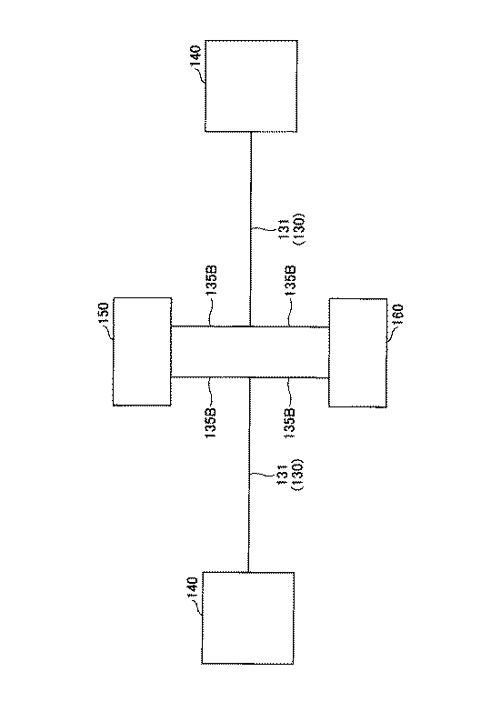
図7及び表1に示すように、実施例1〜4では、電極の引張弾性率は0.003GPa〜0.020GPaの範囲内であった。一方、比較例1では、電極の引張弾性率は1.0GPaであった。 As shown in FIGS. 7 and 1, in Examples 1 to 4, the tensile elastic modulus of the electrode was in the range of 0.003 GPa to 0.020 GPa. On the other hand, in Comparative Example 1, the tensile elastic modulus of the electrode was 1.0 GPa.
よって、電極の表層部におけるM2/M1が5.77〜320.5の範囲内であれば、電極は引張弾性率を0.003GPa〜0.020GPaにでき、好適な伸縮性を有しつつ導電性を有することができるといえることが確認された。したがって、一実施形態に係る電極は、生体センサの電極として用いた際、安定した粘着力及び導電性を有することができる。そのため、生体センサを被験者の肌に密着させて長時間(例えば、24時間)継続して心電図を測定するのに有効に用いることができるといえる。 Therefore, if M2 / M1 on the surface layer of the electrode is within the range of 5.77 to 320.5, the electrode can have a tensile elastic modulus of 0.003 GPa to 0.020 GPa, and is conductive while having suitable elasticity. It was confirmed that it can be said that it can have sex. Therefore, the electrode according to one embodiment can have stable adhesive strength and conductivity when used as an electrode of a biosensor. Therefore, it can be said that the biosensor can be effectively used to bring the biosensor into close contact with the skin of the subject and continuously measure the electrocardiogram for a long time (for example, 24 hours).
以上の通り、実施形態を説明したが、上記実施形態は、例として提示したものであり、上記実施形態により本発明が限定されるものではない。上記実施形態は、その他の様々な形態で実施されることが可能であり、発明の要旨を逸脱しない範囲で、種々の組み合わせ、省略、置き換え、変更等を行うことが可能である。これら実施形態やその変形は、発明の範囲や要旨に含まれると共に、特許請求の範囲に記載された発明とその均等の範囲に含まれる。 Although the embodiments have been described above, the above embodiments are presented as examples, and the present invention is not limited to the above embodiments. The above-described embodiment can be implemented in various other forms, and various combinations, omissions, replacements, changes, etc. can be made without departing from the gist of the invention. These embodiments and modifications thereof are included in the scope and gist of the invention, and are also included in the scope of the invention described in the claims and the equivalent scope thereof.
10 電極
11、12 主面
13、140A 孔
100 貼付型生体センサ(生体センサ)
110 感圧接着層
120 基材層
130 回路部
140 プローブ
150 電子装置
160 電池
170 カバー
10
110 Pressure-
Claims (5)
前記電極の表面から深さ1μm以下の表層部における、前記導電性高分子の含有量に対する前記可塑剤の含有量の割合が、0.5〜500.0である電極。 A plate-shaped electrode containing a conductive polymer, a binder resin, and a plasticizer, and having a pair of main surfaces parallel to each other.
An electrode in which the ratio of the content of the plasticizer to the content of the conductive polymer in the surface layer portion having a depth of 1 μm or less from the surface of the electrode is 0.5 to 500.0.
前記電極の一方の主面側に設置される感圧接着層と、
を含む生体センサ。 The electrode according to any one of claims 1 to 4,
A pressure-sensitive adhesive layer installed on one main surface side of the electrode and
Biosensors including.
Priority Applications (5)
| Application Number | Priority Date | Filing Date | Title |
|---|---|---|---|
| JP2019042985A JP2020142014A (en) | 2019-03-08 | 2019-03-08 | Electrode and biological sensor |
| PCT/JP2020/008643 WO2020184249A1 (en) | 2019-03-08 | 2020-03-02 | Electrode and biosensor |
| CN202080018974.6A CN113543707A (en) | 2019-03-08 | 2020-03-02 | Electrode and biosensor |
| US17/436,583 US20220142540A1 (en) | 2019-03-08 | 2020-03-02 | Electrode and biosensor |
| EP20769578.4A EP3936040A4 (en) | 2019-03-08 | 2020-03-02 | Electrode and biosensor |
Applications Claiming Priority (1)
| Application Number | Priority Date | Filing Date | Title |
|---|---|---|---|
| JP2019042985A JP2020142014A (en) | 2019-03-08 | 2019-03-08 | Electrode and biological sensor |
Publications (1)
| Publication Number | Publication Date |
|---|---|
| JP2020142014A true JP2020142014A (en) | 2020-09-10 |
Family
ID=72354992
Family Applications (1)
| Application Number | Title | Priority Date | Filing Date |
|---|---|---|---|
| JP2019042985A Pending JP2020142014A (en) | 2019-03-08 | 2019-03-08 | Electrode and biological sensor |
Country Status (5)
| Country | Link |
|---|---|
| US (1) | US20220142540A1 (en) |
| EP (1) | EP3936040A4 (en) |
| JP (1) | JP2020142014A (en) |
| CN (1) | CN113543707A (en) |
| WO (1) | WO2020184249A1 (en) |
Cited By (1)
| Publication number | Priority date | Publication date | Assignee | Title |
|---|---|---|---|---|
| WO2021200859A1 (en) * | 2020-03-30 | 2021-10-07 | 日東電工株式会社 | Electrode and biosensor using same |
Citations (6)
| Publication number | Priority date | Publication date | Assignee | Title |
|---|---|---|---|---|
| JPS61137539A (en) * | 1984-12-10 | 1986-06-25 | 積水化学工業株式会社 | Medical conductive pressure-sensitive agent and skin electrode using the same |
| JPH05207983A (en) * | 1991-11-15 | 1993-08-20 | Minnesota Mining & Mfg Co <3M> | Biological medical treatment electrode containing solid conductive polymer composition |
| WO2017183463A1 (en) * | 2016-04-18 | 2017-10-26 | 東レ株式会社 | Electrically conductive fiber structure, electrode member, and method for manufacturing electrically conductive fiber structure |
| JP2018103057A (en) * | 2011-11-17 | 2018-07-05 | 日本電信電話株式会社 | Bioelectrode |
| WO2018198456A1 (en) * | 2017-04-28 | 2018-11-01 | 日東電工株式会社 | Sheet for biosensor |
| JP2019034440A (en) * | 2017-08-10 | 2019-03-07 | 日本電信電話株式会社 | Conductive polymer electrode, and manufacturing method of the same |
Family Cites Families (8)
| Publication number | Priority date | Publication date | Assignee | Title |
|---|---|---|---|---|
| JP3884995B2 (en) | 2002-05-29 | 2007-02-21 | 日東電工株式会社 | Adhesive sheet for skin application |
| JP4925545B2 (en) | 2002-08-23 | 2012-04-25 | 日東電工株式会社 | Adhesive material for skin application |
| JP5544600B2 (en) | 2010-06-30 | 2014-07-09 | 独立行政法人科学技術振興機構 | Biocompatible polymer substrate |
| WO2012056774A1 (en) * | 2010-10-29 | 2012-05-03 | リンテック株式会社 | Transparent conductive film, electronic device, and method for manufacturing electronic device |
| JP6106148B2 (en) * | 2013-11-27 | 2017-03-29 | 日東電工株式会社 | Conductive adhesive tape, electronic member and adhesive |
| JP2016166436A (en) | 2015-03-10 | 2016-09-15 | 日本合成化学工業株式会社 | Laminate, thermosensitive recording medium, and inkjet recording medium |
| JP6984241B2 (en) | 2017-08-31 | 2021-12-17 | セイコーエプソン株式会社 | Liquid tank |
| JP7418944B2 (en) * | 2017-09-11 | 2024-01-22 | 日東電工株式会社 | Conductive compositions and biosensors |
-
2019
- 2019-03-08 JP JP2019042985A patent/JP2020142014A/en active Pending
-
2020
- 2020-03-02 CN CN202080018974.6A patent/CN113543707A/en active Pending
- 2020-03-02 WO PCT/JP2020/008643 patent/WO2020184249A1/en active Application Filing
- 2020-03-02 EP EP20769578.4A patent/EP3936040A4/en active Pending
- 2020-03-02 US US17/436,583 patent/US20220142540A1/en active Pending
Patent Citations (6)
| Publication number | Priority date | Publication date | Assignee | Title |
|---|---|---|---|---|
| JPS61137539A (en) * | 1984-12-10 | 1986-06-25 | 積水化学工業株式会社 | Medical conductive pressure-sensitive agent and skin electrode using the same |
| JPH05207983A (en) * | 1991-11-15 | 1993-08-20 | Minnesota Mining & Mfg Co <3M> | Biological medical treatment electrode containing solid conductive polymer composition |
| JP2018103057A (en) * | 2011-11-17 | 2018-07-05 | 日本電信電話株式会社 | Bioelectrode |
| WO2017183463A1 (en) * | 2016-04-18 | 2017-10-26 | 東レ株式会社 | Electrically conductive fiber structure, electrode member, and method for manufacturing electrically conductive fiber structure |
| WO2018198456A1 (en) * | 2017-04-28 | 2018-11-01 | 日東電工株式会社 | Sheet for biosensor |
| JP2019034440A (en) * | 2017-08-10 | 2019-03-07 | 日本電信電話株式会社 | Conductive polymer electrode, and manufacturing method of the same |
Non-Patent Citations (1)
| Title |
|---|
| CHENGXIN HU ET AL.: "Stable, Strain-Sensitive Conductive Hydrogel with Antifreezing Capability, Remoldability, and Reusab", APPLIED MATERIALS & INTERFACES, vol. 10, no. 50, JPN6022028902, 19 December 2018 (2018-12-19), US, pages 44000 - 44002, ISSN: 0004892505 * |
Cited By (1)
| Publication number | Priority date | Publication date | Assignee | Title |
|---|---|---|---|---|
| WO2021200859A1 (en) * | 2020-03-30 | 2021-10-07 | 日東電工株式会社 | Electrode and biosensor using same |
Also Published As
| Publication number | Publication date |
|---|---|
| WO2020184249A1 (en) | 2020-09-17 |
| US20220142540A1 (en) | 2022-05-12 |
| EP3936040A1 (en) | 2022-01-12 |
| EP3936040A4 (en) | 2022-04-20 |
| CN113543707A (en) | 2021-10-22 |
Similar Documents
| Publication | Publication Date | Title |
|---|---|---|
| Kim et al. | Epidermal electronics | |
| JP6886540B2 (en) | Data acquisition device and biosensor | |
| WO2021076054A1 (en) | Polymer composites, methods of fabrication and uses thereof | |
| JP6814899B2 (en) | Biosensor | |
| WO2020184249A1 (en) | Electrode and biosensor | |
| WO2020184346A1 (en) | Biosensor | |
| JP6886538B2 (en) | Stick-on biosensor | |
| JP2020151104A (en) | Sticking type biological sensor | |
| WO2020195796A1 (en) | Electrode joining structure and biological sensor | |
| WO2020196097A1 (en) | Stick-on biosensor | |
| JP2020142013A (en) | Manufacturing method for electrode sheet | |
| WO2021200805A1 (en) | Biosensor | |
| Minakata et al. | BIOSENSOR | |
| JP2020145156A (en) | Manufacturing method of conductive material | |
| JP7397041B2 (en) | biosensor | |
| WO2023054267A1 (en) | Electrode pad and biometric sensor | |
| WO2023234332A1 (en) | Biosensor | |
| WO2022107710A1 (en) | Biosensor | |
| JP2020151105A (en) | Sticking type biological sensor | |
| WO2023120326A1 (en) | Biosensor | |
| WO2024024694A1 (en) | Biological adhesive and biosensor | |
| JP2020146237A (en) | Sticking type biological sensor | |
| CN116507278A (en) | Biosensor | |
| JP2020142005A (en) | Sticking type sensor |
Legal Events
| Date | Code | Title | Description |
|---|---|---|---|
| A621 | Written request for application examination |
Free format text: JAPANESE INTERMEDIATE CODE: A621 Effective date: 20220125 |
|
| A131 | Notification of reasons for refusal |
Free format text: JAPANESE INTERMEDIATE CODE: A131 Effective date: 20220712 |
|
| A521 | Request for written amendment filed |
Free format text: JAPANESE INTERMEDIATE CODE: A523 Effective date: 20220906 |
|
| A02 | Decision of refusal |
Free format text: JAPANESE INTERMEDIATE CODE: A02 Effective date: 20221011 |
|
| A521 | Request for written amendment filed |
Free format text: JAPANESE INTERMEDIATE CODE: A523 Effective date: 20230110 |
|
| C60 | Trial request (containing other claim documents, opposition documents) |
Free format text: JAPANESE INTERMEDIATE CODE: C60 Effective date: 20230110 |
|
| A911 | Transfer to examiner for re-examination before appeal (zenchi) |
Free format text: JAPANESE INTERMEDIATE CODE: A911 Effective date: 20230118 |
|
| C21 | Notice of transfer of a case for reconsideration by examiners before appeal proceedings |
Free format text: JAPANESE INTERMEDIATE CODE: C21 Effective date: 20230124 |
|
| A912 | Re-examination (zenchi) completed and case transferred to appeal board |
Free format text: JAPANESE INTERMEDIATE CODE: A912 Effective date: 20230310 |
|
| C211 | Notice of termination of reconsideration by examiners before appeal proceedings |
Free format text: JAPANESE INTERMEDIATE CODE: C211 Effective date: 20230314 |