JP2020053475A - Thin-film transistor and display device - Google Patents
Thin-film transistor and display device Download PDFInfo
- Publication number
- JP2020053475A JP2020053475A JP2018179131A JP2018179131A JP2020053475A JP 2020053475 A JP2020053475 A JP 2020053475A JP 2018179131 A JP2018179131 A JP 2018179131A JP 2018179131 A JP2018179131 A JP 2018179131A JP 2020053475 A JP2020053475 A JP 2020053475A
- Authority
- JP
- Japan
- Prior art keywords
- layer
- insulating layer
- gate insulating
- gate
- electrode
- Prior art date
- Legal status (The legal status is an assumption and is not a legal conclusion. Google has not performed a legal analysis and makes no representation as to the accuracy of the status listed.)
- Pending
Links
- 239000010409 thin film Substances 0.000 title claims abstract description 19
- 239000004065 semiconductor Substances 0.000 claims abstract description 48
- 239000001257 hydrogen Substances 0.000 claims abstract description 28
- 229910052739 hydrogen Inorganic materials 0.000 claims abstract description 28
- 229910052738 indium Inorganic materials 0.000 claims abstract description 12
- APFVFJFRJDLVQX-UHFFFAOYSA-N indium atom Chemical compound [In] APFVFJFRJDLVQX-UHFFFAOYSA-N 0.000 claims abstract description 12
- GYHNNYVSQQEPJS-UHFFFAOYSA-N Gallium Chemical compound [Ga] GYHNNYVSQQEPJS-UHFFFAOYSA-N 0.000 claims abstract description 7
- 229910052733 gallium Inorganic materials 0.000 claims abstract description 7
- 125000004435 hydrogen atom Chemical group [H]* 0.000 claims abstract description 3
- 229910052581 Si3N4 Inorganic materials 0.000 claims description 18
- HQVNEWCFYHHQES-UHFFFAOYSA-N silicon nitride Chemical group N12[Si]34N5[Si]62N3[Si]51N64 HQVNEWCFYHHQES-UHFFFAOYSA-N 0.000 claims description 18
- VYPSYNLAJGMNEJ-UHFFFAOYSA-N Silicium dioxide Chemical group O=[Si]=O VYPSYNLAJGMNEJ-UHFFFAOYSA-N 0.000 claims description 13
- 229910052814 silicon oxide Inorganic materials 0.000 claims description 11
- 239000000758 substrate Substances 0.000 abstract description 28
- 238000004519 manufacturing process Methods 0.000 abstract description 14
- 239000010410 layer Substances 0.000 description 320
- UFHFLCQGNIYNRP-UHFFFAOYSA-N Hydrogen Chemical compound [H][H] UFHFLCQGNIYNRP-UHFFFAOYSA-N 0.000 description 23
- 239000010408 film Substances 0.000 description 20
- 239000000463 material Substances 0.000 description 10
- 239000012044 organic layer Substances 0.000 description 9
- 239000000956 alloy Substances 0.000 description 8
- 229910045601 alloy Inorganic materials 0.000 description 8
- 238000000034 method Methods 0.000 description 8
- 238000009792 diffusion process Methods 0.000 description 7
- 229910052751 metal Inorganic materials 0.000 description 7
- 239000011347 resin Substances 0.000 description 7
- 229920005989 resin Polymers 0.000 description 7
- 230000015572 biosynthetic process Effects 0.000 description 6
- 239000002184 metal Substances 0.000 description 6
- 229910052782 aluminium Inorganic materials 0.000 description 5
- XAGFODPZIPBFFR-UHFFFAOYSA-N aluminium Chemical compound [Al] XAGFODPZIPBFFR-UHFFFAOYSA-N 0.000 description 5
- 230000000903 blocking effect Effects 0.000 description 5
- 229910044991 metal oxide Inorganic materials 0.000 description 5
- 150000004706 metal oxides Chemical class 0.000 description 5
- 238000007789 sealing Methods 0.000 description 5
- RTAQQCXQSZGOHL-UHFFFAOYSA-N Titanium Chemical compound [Ti] RTAQQCXQSZGOHL-UHFFFAOYSA-N 0.000 description 4
- 230000004888 barrier function Effects 0.000 description 4
- 239000004020 conductor Substances 0.000 description 4
- PMHQVHHXPFUNSP-UHFFFAOYSA-M copper(1+);methylsulfanylmethane;bromide Chemical compound Br[Cu].CSC PMHQVHHXPFUNSP-UHFFFAOYSA-M 0.000 description 4
- 238000010586 diagram Methods 0.000 description 4
- 239000004973 liquid crystal related substance Substances 0.000 description 4
- 238000005259 measurement Methods 0.000 description 4
- 229910052709 silver Inorganic materials 0.000 description 4
- 239000004332 silver Substances 0.000 description 4
- 229920001187 thermosetting polymer Polymers 0.000 description 4
- 229910052719 titanium Inorganic materials 0.000 description 4
- 239000010936 titanium Substances 0.000 description 4
- VYZAMTAEIAYCRO-UHFFFAOYSA-N Chromium Chemical compound [Cr] VYZAMTAEIAYCRO-UHFFFAOYSA-N 0.000 description 3
- ZOKXTWBITQBERF-UHFFFAOYSA-N Molybdenum Chemical compound [Mo] ZOKXTWBITQBERF-UHFFFAOYSA-N 0.000 description 3
- 229910052795 boron group element Inorganic materials 0.000 description 3
- 239000003990 capacitor Substances 0.000 description 3
- 229910052804 chromium Inorganic materials 0.000 description 3
- 239000011651 chromium Substances 0.000 description 3
- 239000011521 glass Substances 0.000 description 3
- 239000012535 impurity Substances 0.000 description 3
- 229910052750 molybdenum Inorganic materials 0.000 description 3
- 239000011733 molybdenum Substances 0.000 description 3
- TWNQGVIAIRXVLR-UHFFFAOYSA-N oxo(oxoalumanyloxy)alumane Chemical compound O=[Al]O[Al]=O TWNQGVIAIRXVLR-UHFFFAOYSA-N 0.000 description 3
- 229910052715 tantalum Inorganic materials 0.000 description 3
- GUVRBAGPIYLISA-UHFFFAOYSA-N tantalum atom Chemical compound [Ta] GUVRBAGPIYLISA-UHFFFAOYSA-N 0.000 description 3
- 238000002834 transmittance Methods 0.000 description 3
- WFKWXMTUELFFGS-UHFFFAOYSA-N tungsten Chemical compound [W] WFKWXMTUELFFGS-UHFFFAOYSA-N 0.000 description 3
- 229910052721 tungsten Inorganic materials 0.000 description 3
- 239000010937 tungsten Substances 0.000 description 3
- IJGRMHOSHXDMSA-UHFFFAOYSA-N Atomic nitrogen Chemical compound N#N IJGRMHOSHXDMSA-UHFFFAOYSA-N 0.000 description 2
- FYYHWMGAXLPEAU-UHFFFAOYSA-N Magnesium Chemical compound [Mg] FYYHWMGAXLPEAU-UHFFFAOYSA-N 0.000 description 2
- 239000000853 adhesive Substances 0.000 description 2
- 230000001070 adhesive effect Effects 0.000 description 2
- 150000001875 compounds Chemical class 0.000 description 2
- 239000013078 crystal Substances 0.000 description 2
- 230000007423 decrease Effects 0.000 description 2
- 150000002431 hydrogen Chemical class 0.000 description 2
- 238000002347 injection Methods 0.000 description 2
- 239000007924 injection Substances 0.000 description 2
- 229910052749 magnesium Inorganic materials 0.000 description 2
- 239000011777 magnesium Substances 0.000 description 2
- 239000007769 metal material Substances 0.000 description 2
- 239000010453 quartz Substances 0.000 description 2
- QGZKDVFQNNGYKY-UHFFFAOYSA-N Ammonia Chemical compound N QGZKDVFQNNGYKY-UHFFFAOYSA-N 0.000 description 1
- XUIMIQQOPSSXEZ-UHFFFAOYSA-N Silicon Chemical compound [Si] XUIMIQQOPSSXEZ-UHFFFAOYSA-N 0.000 description 1
- ATJFFYVFTNAWJD-UHFFFAOYSA-N Tin Chemical compound [Sn] ATJFFYVFTNAWJD-UHFFFAOYSA-N 0.000 description 1
- HCHKCACWOHOZIP-UHFFFAOYSA-N Zinc Chemical compound [Zn] HCHKCACWOHOZIP-UHFFFAOYSA-N 0.000 description 1
- QCWXUUIWCKQGHC-UHFFFAOYSA-N Zirconium Chemical compound [Zr] QCWXUUIWCKQGHC-UHFFFAOYSA-N 0.000 description 1
- 230000002411 adverse Effects 0.000 description 1
- QVGXLLKOCUKJST-UHFFFAOYSA-N atomic oxygen Chemical compound [O] QVGXLLKOCUKJST-UHFFFAOYSA-N 0.000 description 1
- 229910052800 carbon group element Inorganic materials 0.000 description 1
- 230000015556 catabolic process Effects 0.000 description 1
- 239000000470 constituent Substances 0.000 description 1
- 239000006059 cover glass Substances 0.000 description 1
- 230000007547 defect Effects 0.000 description 1
- 238000001514 detection method Methods 0.000 description 1
- 230000009977 dual effect Effects 0.000 description 1
- 230000005684 electric field Effects 0.000 description 1
- 238000005530 etching Methods 0.000 description 1
- 229910021480 group 4 element Inorganic materials 0.000 description 1
- 229910000449 hafnium oxide Inorganic materials 0.000 description 1
- WIHZLLGSGQNAGK-UHFFFAOYSA-N hafnium(4+);oxygen(2-) Chemical compound [O-2].[O-2].[Hf+4] WIHZLLGSGQNAGK-UHFFFAOYSA-N 0.000 description 1
- 238000010438 heat treatment Methods 0.000 description 1
- 230000005525 hole transport Effects 0.000 description 1
- 238000010348 incorporation Methods 0.000 description 1
- 230000014759 maintenance of location Effects 0.000 description 1
- 239000013081 microcrystal Substances 0.000 description 1
- 239000000203 mixture Substances 0.000 description 1
- 229910052757 nitrogen Inorganic materials 0.000 description 1
- 230000003287 optical effect Effects 0.000 description 1
- 239000001301 oxygen Substances 0.000 description 1
- 229910052760 oxygen Inorganic materials 0.000 description 1
- 239000002245 particle Substances 0.000 description 1
- 238000005192 partition Methods 0.000 description 1
- 238000000059 patterning Methods 0.000 description 1
- 230000000149 penetrating effect Effects 0.000 description 1
- 230000035515 penetration Effects 0.000 description 1
- 230000002093 peripheral effect Effects 0.000 description 1
- 238000000206 photolithography Methods 0.000 description 1
- -1 polycrystal Substances 0.000 description 1
- 238000002310 reflectometry Methods 0.000 description 1
- 230000035945 sensitivity Effects 0.000 description 1
- 229910052710 silicon Inorganic materials 0.000 description 1
- 239000010703 silicon Substances 0.000 description 1
- 239000002356 single layer Substances 0.000 description 1
- 238000009751 slip forming Methods 0.000 description 1
- 239000002344 surface layer Substances 0.000 description 1
- 229910052725 zinc Inorganic materials 0.000 description 1
- 239000011701 zinc Substances 0.000 description 1
- 229910052726 zirconium Inorganic materials 0.000 description 1
Images


Classifications
-
- H—ELECTRICITY
- H10—SEMICONDUCTOR DEVICES; ELECTRIC SOLID-STATE DEVICES NOT OTHERWISE PROVIDED FOR
- H10K—ORGANIC ELECTRIC SOLID-STATE DEVICES
- H10K59/00—Integrated devices, or assemblies of multiple devices, comprising at least one organic light-emitting element covered by group H10K50/00
- H10K59/10—OLED displays
- H10K59/12—Active-matrix OLED [AMOLED] displays
- H10K59/121—Active-matrix OLED [AMOLED] displays characterised by the geometry or disposition of pixel elements
- H10K59/1213—Active-matrix OLED [AMOLED] displays characterised by the geometry or disposition of pixel elements the pixel elements being TFTs
-
- H—ELECTRICITY
- H01—ELECTRIC ELEMENTS
- H01L—SEMICONDUCTOR DEVICES NOT COVERED BY CLASS H10
- H01L29/00—Semiconductor devices adapted for rectifying, amplifying, oscillating or switching, or capacitors or resistors with at least one potential-jump barrier or surface barrier, e.g. PN junction depletion layer or carrier concentration layer; Details of semiconductor bodies or of electrodes thereof ; Multistep manufacturing processes therefor
- H01L29/66—Types of semiconductor device ; Multistep manufacturing processes therefor
- H01L29/68—Types of semiconductor device ; Multistep manufacturing processes therefor controllable by only the electric current supplied, or only the electric potential applied, to an electrode which does not carry the current to be rectified, amplified or switched
- H01L29/76—Unipolar devices, e.g. field effect transistors
- H01L29/772—Field effect transistors
- H01L29/78—Field effect transistors with field effect produced by an insulated gate
- H01L29/786—Thin film transistors, i.e. transistors with a channel being at least partly a thin film
- H01L29/78645—Thin film transistors, i.e. transistors with a channel being at least partly a thin film with multiple gate
- H01L29/78648—Thin film transistors, i.e. transistors with a channel being at least partly a thin film with multiple gate arranged on opposing sides of the channel
-
- G—PHYSICS
- G09—EDUCATION; CRYPTOGRAPHY; DISPLAY; ADVERTISING; SEALS
- G09F—DISPLAYING; ADVERTISING; SIGNS; LABELS OR NAME-PLATES; SEALS
- G09F9/00—Indicating arrangements for variable information in which the information is built-up on a support by selection or combination of individual elements
- G09F9/30—Indicating arrangements for variable information in which the information is built-up on a support by selection or combination of individual elements in which the desired character or characters are formed by combining individual elements
-
- H—ELECTRICITY
- H01—ELECTRIC ELEMENTS
- H01L—SEMICONDUCTOR DEVICES NOT COVERED BY CLASS H10
- H01L27/00—Devices consisting of a plurality of semiconductor or other solid-state components formed in or on a common substrate
- H01L27/02—Devices consisting of a plurality of semiconductor or other solid-state components formed in or on a common substrate including semiconductor components specially adapted for rectifying, oscillating, amplifying or switching and having at least one potential-jump barrier or surface barrier; including integrated passive circuit elements with at least one potential-jump barrier or surface barrier
- H01L27/12—Devices consisting of a plurality of semiconductor or other solid-state components formed in or on a common substrate including semiconductor components specially adapted for rectifying, oscillating, amplifying or switching and having at least one potential-jump barrier or surface barrier; including integrated passive circuit elements with at least one potential-jump barrier or surface barrier the substrate being other than a semiconductor body, e.g. an insulating body
- H01L27/1214—Devices consisting of a plurality of semiconductor or other solid-state components formed in or on a common substrate including semiconductor components specially adapted for rectifying, oscillating, amplifying or switching and having at least one potential-jump barrier or surface barrier; including integrated passive circuit elements with at least one potential-jump barrier or surface barrier the substrate being other than a semiconductor body, e.g. an insulating body comprising a plurality of TFTs formed on a non-semiconducting substrate, e.g. driving circuits for AMLCDs
- H01L27/1222—Devices consisting of a plurality of semiconductor or other solid-state components formed in or on a common substrate including semiconductor components specially adapted for rectifying, oscillating, amplifying or switching and having at least one potential-jump barrier or surface barrier; including integrated passive circuit elements with at least one potential-jump barrier or surface barrier the substrate being other than a semiconductor body, e.g. an insulating body comprising a plurality of TFTs formed on a non-semiconducting substrate, e.g. driving circuits for AMLCDs with a particular composition, shape or crystalline structure of the active layer
- H01L27/1225—Devices consisting of a plurality of semiconductor or other solid-state components formed in or on a common substrate including semiconductor components specially adapted for rectifying, oscillating, amplifying or switching and having at least one potential-jump barrier or surface barrier; including integrated passive circuit elements with at least one potential-jump barrier or surface barrier the substrate being other than a semiconductor body, e.g. an insulating body comprising a plurality of TFTs formed on a non-semiconducting substrate, e.g. driving circuits for AMLCDs with a particular composition, shape or crystalline structure of the active layer with semiconductor materials not belonging to the group IV of the periodic table, e.g. InGaZnO
-
- H—ELECTRICITY
- H01—ELECTRIC ELEMENTS
- H01L—SEMICONDUCTOR DEVICES NOT COVERED BY CLASS H10
- H01L29/00—Semiconductor devices adapted for rectifying, amplifying, oscillating or switching, or capacitors or resistors with at least one potential-jump barrier or surface barrier, e.g. PN junction depletion layer or carrier concentration layer; Details of semiconductor bodies or of electrodes thereof ; Multistep manufacturing processes therefor
- H01L29/40—Electrodes ; Multistep manufacturing processes therefor
- H01L29/41—Electrodes ; Multistep manufacturing processes therefor characterised by their shape, relative sizes or dispositions
- H01L29/423—Electrodes ; Multistep manufacturing processes therefor characterised by their shape, relative sizes or dispositions not carrying the current to be rectified, amplified or switched
- H01L29/42312—Gate electrodes for field effect devices
- H01L29/42316—Gate electrodes for field effect devices for field-effect transistors
- H01L29/4232—Gate electrodes for field effect devices for field-effect transistors with insulated gate
- H01L29/42384—Gate electrodes for field effect devices for field-effect transistors with insulated gate for thin film field effect transistors, e.g. characterised by the thickness or the shape of the insulator or the dimensions, the shape or the lay-out of the conductor
-
- H—ELECTRICITY
- H01—ELECTRIC ELEMENTS
- H01L—SEMICONDUCTOR DEVICES NOT COVERED BY CLASS H10
- H01L29/00—Semiconductor devices adapted for rectifying, amplifying, oscillating or switching, or capacitors or resistors with at least one potential-jump barrier or surface barrier, e.g. PN junction depletion layer or carrier concentration layer; Details of semiconductor bodies or of electrodes thereof ; Multistep manufacturing processes therefor
- H01L29/40—Electrodes ; Multistep manufacturing processes therefor
- H01L29/43—Electrodes ; Multistep manufacturing processes therefor characterised by the materials of which they are formed
- H01L29/49—Metal-insulator-semiconductor electrodes, e.g. gates of MOSFET
- H01L29/4908—Metal-insulator-semiconductor electrodes, e.g. gates of MOSFET for thin film semiconductor, e.g. gate of TFT
-
- H—ELECTRICITY
- H01—ELECTRIC ELEMENTS
- H01L—SEMICONDUCTOR DEVICES NOT COVERED BY CLASS H10
- H01L29/00—Semiconductor devices adapted for rectifying, amplifying, oscillating or switching, or capacitors or resistors with at least one potential-jump barrier or surface barrier, e.g. PN junction depletion layer or carrier concentration layer; Details of semiconductor bodies or of electrodes thereof ; Multistep manufacturing processes therefor
- H01L29/66—Types of semiconductor device ; Multistep manufacturing processes therefor
- H01L29/68—Types of semiconductor device ; Multistep manufacturing processes therefor controllable by only the electric current supplied, or only the electric potential applied, to an electrode which does not carry the current to be rectified, amplified or switched
- H01L29/76—Unipolar devices, e.g. field effect transistors
- H01L29/772—Field effect transistors
- H01L29/78—Field effect transistors with field effect produced by an insulated gate
- H01L29/786—Thin film transistors, i.e. transistors with a channel being at least partly a thin film
- H01L29/7869—Thin film transistors, i.e. transistors with a channel being at least partly a thin film having a semiconductor body comprising an oxide semiconductor material, e.g. zinc oxide, copper aluminium oxide, cadmium stannate
-
- H—ELECTRICITY
- H10—SEMICONDUCTOR DEVICES; ELECTRIC SOLID-STATE DEVICES NOT OTHERWISE PROVIDED FOR
- H10K—ORGANIC ELECTRIC SOLID-STATE DEVICES
- H10K50/00—Organic light-emitting devices
-
- H—ELECTRICITY
- H01—ELECTRIC ELEMENTS
- H01L—SEMICONDUCTOR DEVICES NOT COVERED BY CLASS H10
- H01L29/00—Semiconductor devices adapted for rectifying, amplifying, oscillating or switching, or capacitors or resistors with at least one potential-jump barrier or surface barrier, e.g. PN junction depletion layer or carrier concentration layer; Details of semiconductor bodies or of electrodes thereof ; Multistep manufacturing processes therefor
- H01L29/40—Electrodes ; Multistep manufacturing processes therefor
- H01L29/41—Electrodes ; Multistep manufacturing processes therefor characterised by their shape, relative sizes or dispositions
- H01L29/423—Electrodes ; Multistep manufacturing processes therefor characterised by their shape, relative sizes or dispositions not carrying the current to be rectified, amplified or switched
- H01L29/42312—Gate electrodes for field effect devices
- H01L29/42316—Gate electrodes for field effect devices for field-effect transistors
- H01L29/4232—Gate electrodes for field effect devices for field-effect transistors with insulated gate
- H01L29/42384—Gate electrodes for field effect devices for field-effect transistors with insulated gate for thin film field effect transistors, e.g. characterised by the thickness or the shape of the insulator or the dimensions, the shape or the lay-out of the conductor
- H01L2029/42388—Gate electrodes for field effect devices for field-effect transistors with insulated gate for thin film field effect transistors, e.g. characterised by the thickness or the shape of the insulator or the dimensions, the shape or the lay-out of the conductor characterised by the shape of the insulating material
-
- H—ELECTRICITY
- H10—SEMICONDUCTOR DEVICES; ELECTRIC SOLID-STATE DEVICES NOT OTHERWISE PROVIDED FOR
- H10K—ORGANIC ELECTRIC SOLID-STATE DEVICES
- H10K50/00—Organic light-emitting devices
- H10K50/80—Constructional details
- H10K50/805—Electrodes
- H10K50/81—Anodes
- H10K50/814—Anodes combined with auxiliary electrodes, e.g. ITO layer combined with metal lines
-
- H—ELECTRICITY
- H10—SEMICONDUCTOR DEVICES; ELECTRIC SOLID-STATE DEVICES NOT OTHERWISE PROVIDED FOR
- H10K—ORGANIC ELECTRIC SOLID-STATE DEVICES
- H10K59/00—Integrated devices, or assemblies of multiple devices, comprising at least one organic light-emitting element covered by group H10K50/00
- H10K59/10—OLED displays
- H10K59/12—Active-matrix OLED [AMOLED] displays
- H10K59/123—Connection of the pixel electrodes to the thin film transistors [TFT]
Abstract
Description
本発明は、薄膜トランジスタ及び表示装置に関する。 The present invention relates to a thin film transistor and a display device.
特許文献1には、ゲート電極層に窒素を含むシリコン膜を含んで構成されるゲート絶縁層と、ゲート絶縁層上の酸化物絶縁層と、酸化物絶縁層上に接する酸化物半導体層を有する半導体装置が開示されている。同文献において、ゲート絶縁層は窒化シリコン膜、酸化物絶縁層は酸化物半導体層の構成元素から選択される一又は複数の金属元素を含む酸化物膜であり、ゲート絶縁層の膜厚は、酸化物絶縁層よりも厚い。 Patent Document 1 includes a gate insulating layer including a silicon film containing nitrogen in a gate electrode layer, an oxide insulating layer over the gate insulating layer, and an oxide semiconductor layer in contact with the oxide insulating layer. A semiconductor device is disclosed. In the document, the gate insulating layer is a silicon nitride film, the oxide insulating layer is an oxide film containing one or more metal elements selected from constituent elements of the oxide semiconductor layer, and the thickness of the gate insulating layer is Thicker than the oxide insulating layer.
インジウム、ガリウム等の第13族元素等を含んだIGO、IGZO等の酸化物半導体を活性層とするトランジスタは、オフリーク電流が非常に小さいため、これを表示装置の駆動素子等に用いた場合には低消費電力を実現できる。また容量と接続するスイッチング素子として用いた場合の電荷保持性能が高いため、各種の応用が期待される。
A transistor having an active layer of an oxide semiconductor such as IGO or IGZO containing a
しかしながら、酸化物半導体は水素に対する感受性が高く、水素に暴露されることにより活性層がn型化し、オフリーク電流を十分に下げることができなくなる。ゲート絶縁層として、窒化シリコンを用いた場合、製膜プロセスに使用されるアンモニアガスに由来する水素が窒化シリコン中に残留し、これが拡散により酸化物半導体に悪影響を及ぼす。この窒化シリコン中の水素の含有量は、フラットパネルディスプレイ製造に用いられるマザーガラスなどの大型の基板に対して窒化シリコン膜を製膜する際には、面内の制御が難しく、その分布が不均一となってしまい、均一な特性のトランジスタを得るのは難しい。 However, an oxide semiconductor has high sensitivity to hydrogen, and an active layer becomes n-type due to exposure to hydrogen, so that an off-leak current cannot be sufficiently reduced. In the case where silicon nitride is used as the gate insulating layer, hydrogen derived from ammonia gas used in the film formation process remains in silicon nitride, which adversely affects the oxide semiconductor by diffusion. When forming a silicon nitride film on a large-sized substrate such as a mother glass used for manufacturing a flat panel display, it is difficult to control the in-plane distribution of the hydrogen content in the silicon nitride. It becomes uniform, and it is difficult to obtain a transistor having uniform characteristics.
あるいは、ゲート絶縁層として酸化シリコンを用いた場合、十分に厚膜として形成すれば、製膜プロセス中の水素の混入は避けられるが、一方で酸化シリコンは比誘電率が4前後と、窒化シリコンの比誘電率である8程度に比べて小さく、十分なドレイン電流を得るためには膜厚を薄くしなければならず、段差のカバレッジ不良や絶縁破壊耐性の低下が心配される。 Alternatively, when silicon oxide is used as the gate insulating layer, if a sufficiently thick film is formed, the incorporation of hydrogen during the film formation process can be avoided, but silicon oxide has a relative dielectric constant of about 4 and silicon nitride. It is smaller than the relative dielectric constant of about 8, and the film thickness must be reduced in order to obtain a sufficient drain current, and there is a concern about poor coverage of steps and a decrease in dielectric breakdown resistance.
本発明は、上記事情に鑑みてなされたものであり、酸化物半導体を活性層とするトランジスタのオフリーク電流を十分に小さくするとともに、大型基板に対して多数のトランジスタを形成する際にも均一な特性が得られ、なおかつ製造工程への負荷を小さくすることを目的とする。 The present invention has been made in view of the above circumstances, and while sufficiently reducing the off-leakage current of a transistor including an oxide semiconductor as an active layer, a uniform uniformity can be obtained when forming a large number of transistors on a large substrate. It is an object to obtain characteristics and reduce the load on the manufacturing process.
上記課題を解決すべく本出願において開示される発明は種々の側面を有しており、それ
ら側面の代表的なものの概要は以下の通りである。
The invention disclosed in the present application has various aspects in order to solve the above-mentioned problems, and typical aspects of the aspects are outlined below.
(1)少なくともインジウム及びガリウムを含む酸化物半導体からなる活性層と、少なくとも1つのゲート電極と、前記活性層と前記ゲート電極間の前記ゲート電極側に配置された第1ゲート絶縁層と、前記活性層と前記ゲート電極化の前記活性層側に配置された水素ブロック層である第2ゲート絶縁層と、を有する薄膜トランジスタ。 (1) an active layer made of an oxide semiconductor containing at least indium and gallium; at least one gate electrode; a first gate insulating layer disposed between the active layer and the gate electrode on the gate electrode side; A thin film transistor comprising: an active layer; and a second gate insulating layer that is a hydrogen block layer disposed on the active layer side of the gate electrode.
(2)(1)において、前記第1ゲート絶縁層は窒化シリコン層であり、前記第2ゲート絶縁層は酸化シリコン層であり、前記第2ゲート絶縁層の厚みが前記第1ゲート絶縁層より厚い薄膜トランジスタ。 (2) In (1), the first gate insulating layer is a silicon nitride layer, the second gate insulating layer is a silicon oxide layer, and the thickness of the second gate insulating layer is greater than that of the first gate insulating layer. Thick thin film transistor.
(3)(2)において、前記第1ゲート絶縁層の厚みは30nm以上400nm以下であり、前記第2ゲート絶縁層の厚みは50nm以上500nm以下であり、前記第1ゲート絶縁層と前記第2ゲート絶縁層の合計の厚みは400nm以上である、薄膜トランジスタ。 (3) In (2), the thickness of the first gate insulating layer is 30 nm or more and 400 nm or less, and the thickness of the second gate insulating layer is 50 nm or more and 500 nm or less. The thin film transistor in which the total thickness of the gate insulating layer is 400 nm or more.
(4)(2)又は(3)において、前記第1ゲート絶縁層と前記第2ゲート絶縁層の厚みの差は50nm以上である、薄膜トランジスタ。 (4) The thin film transistor according to (2) or (3), wherein a difference in thickness between the first gate insulating layer and the second gate insulating layer is 50 nm or more.
(5)(2)〜(4)のいずれかにおいて、前記第1ゲート絶縁層と前記第2ゲート絶縁層の合計の厚みは600nm以下である、薄膜トランジスタ。 (5) The thin film transistor according to any one of (2) to (4), wherein a total thickness of the first gate insulating layer and the second gate insulating layer is 600 nm or less.
(6)(1)〜(5)のいずれかにおいて、前記ゲート電極は、前記活性層の下部に設けられた下部ゲート電極と、前記活性層の上部に設けられた上部ゲート電極からなる、薄膜トランジスタ。 (6) The thin film transistor according to any one of (1) to (5), wherein the gate electrode includes a lower gate electrode provided below the active layer and an upper gate electrode provided above the active layer. .
(7)(1)〜(6)のいずれかの薄膜トランジスタを用いた表示装置。 (7) A display device using the thin film transistor according to any one of (1) to (6).
図1は本発明の実施形態に係るトランジスタ10の断面を説明する図である。
FIG. 1 is a diagram illustrating a cross section of a
トランジスタ10は、基板1上に形成されたアンダーコート層2上にフォトリソグラフィの手法を用いて形成されたいわゆる薄膜トランジスタである。本実施形態では、トランジスタ10は、活性層である酸化物半導体層13の上下にそれぞれゲート電極を有する、いわゆるデュアルゲート構造であるが、これに替えて、酸化物半導体層13の上下いずれか片側のみにゲート電極を有する、いわゆるスタガ型、あるいは逆スタガ型の構造であってもよい。
The
基板1は、ガラス基板、石英基板、樹脂基板等の無機又は有機基板であり、剛性を持つものであっても、可撓性を持つものであってもよい。また、アンダーコート層2は、不純物に対するバリア層として機能する膜である。アンダーコート層2上には、下部ゲート電極層11が形成される。下部ゲート電極層11は金属若しくは合金層、又は導電性金属酸化物やその他の導電性材料からなってよく、好ましくは低抵抗性の材料を選択する。
The substrate 1 is an inorganic or organic substrate such as a glass substrate, a quartz substrate, and a resin substrate, and may be rigid or flexible. The
下部ゲート電極層11上に、下部ゲート絶縁層12が形成される。下部ゲート絶縁層12は、ゲート電極層11と接する下部第1ゲート絶縁層121と、下部ゲート絶縁層12上に形成される酸化物半導体層13と接する下部第2ゲート絶縁層122を含み、下部第1ゲート絶縁層121と下部第2ゲート絶縁層122はその材質が異なる。ここでは、下部第1ゲート絶縁層121は、組成あるいは製造プロセス上の理由から、内部に水素を含有する層である。一方、下部第2ゲート絶縁層122は、内部に水素を事実上含まない層であり、下部第1ゲート絶縁層121から酸化物半導体層13への水素の拡散を妨げる、水素ブロック層として機能する層である。
On the lower
本実施形態では、下部第1ゲート絶縁層121は窒化シリコン、下部第2ゲート絶縁層122は酸化シリコン層であり、比誘電率は下部第1ゲート絶縁層121がおよそ8に対し、下部第2ゲート絶縁層122は4であって、下部第1ゲート絶縁層121の方が比誘電率が大きい。下部第1ゲート絶縁層121の厚みは30nm以上400nm以下、好ましくは50nm以上300nm以下とし、より好ましくは100nm以上200nm以下とする。また、下部第2ゲート絶縁層122の厚みは50nm以上500nm以下、好ましくは100nm以下400nm以下とし、より好ましくは200nm以上300nm以下とする。また、下部第1ゲート絶縁層121と下部第2ゲート絶縁層122の合計の厚みは400nm以上とする。下部第1ゲート絶縁層121と下部第2ゲート絶縁層122の合計の厚みの上限は必ずしも設ける必要はないが、製膜時間の観点から、600nm以下とすることが製造上好ましい。
In the present embodiment, the lower first
また、下部第2ゲート絶縁層122の厚みは下部第1ゲート絶縁層121の厚みより厚くすることが望ましい。そして、下部第2ゲート絶縁層122の厚みと下部第1ゲート絶縁層121の厚みとの差は、好ましくは50nm以上とし、より好ましくは100nm以上とする。
It is preferable that the thickness of the lower second
以上の下部第1ゲート絶縁層121と下部第2ゲート絶縁層122を積層する理由は、下部第1ゲート絶縁層121は製造工程により組織中に水素を含有するため、酸化物半導体層13と直接接触させることなく、水素の酸化物半導体層13への拡散を妨げることにある。そのため、下部第2ゲート絶縁層122は、下部第1ゲート絶縁層121から酸化物半導体層13への水素の拡散を妨げる性能が必要であるが、本実施形態で下部第2ゲート絶縁層122に用いている酸化シリコンは、拡散による水素の組織中への侵入を防ぐ性質は持っていない。そのため、下部第2ゲート絶縁層122には、トランジスタ10の製造工程における加熱等により、下部第1ゲート絶縁層121からの水素の拡散が生じたとしても、実質的に水素が下部第2ゲート絶縁層122を透過することのない厚みが必要であり、それ故に下部第1ゲート絶縁層121よりも厚みが厚い必要がある。
The reason why the lower first
一方で、酸化シリコンは前述の通り誘電率が低いため、ゲート絶縁層12を酸化シリコンのみで生成すると、ドレイン電流の不足が生じるか、または厚膜化によるプロセスコストの増大が生じるため、誘電率の高い窒化シリコンによる下部第1ゲート絶縁層121を、酸化物半導体層13からできるだけ離れた、下部ゲート電極層11と接する位置に設け、ゲート絶縁層12全体での誘電率を高める。ゲート絶縁層12全体での誘電率を十分に確保するためと、水素の酸化物半導体層13への拡散を抑制するため、下部第1ゲート絶縁層121と下部第2ゲート絶縁層122の合計の厚みは400nm以上とする。
On the other hand, since the silicon oxide has a low dielectric constant as described above, if the
なお、下部第2ゲート絶縁層122の材質として、酸化シリコン以外の材質を用いてもよい。水素ブロック性能が高く、誘電率も高い材質であれば、下部第2ゲート絶縁層122の厚みは上記数値範囲に限定されることなく設定してもよい。そのような材質の例としては、酸化アルミニウムや酸化ハフニウムを挙げることができる。
Note that a material other than silicon oxide may be used as the material of the lower second
さらに、下部ゲート絶縁層12上であって、下部ゲート電極層11に重畳する領域に、酸化物半導体層13が形成される。酸化物半導体層13は、トランジスタ10の活性層であり、第13族元素の内、少なくともインジウム及びガリウムを含む金属酸化物である。本実施形態では、酸化物半導体層13は、いわゆるIGZOとして知られるインジウム、ガリウム及び亜鉛の酸化物からなる透明半導体である。
Further, an
酸化物半導体層13及びゲート絶縁層12上に、酸化物半導体層13に一部分が接するように、電極層14が形成される。電極層14は、パターニングにより、ソース電極及びドレイン電極としての形状を有し、酸化物半導体層13上で互いに接することなく、所定の距離を離して配置される。そのため、酸化物半導体層13上には、電極層14に覆われない部分が存在する。電極層14は、下部ゲート電極11と同様に、金属若しくは合金層、又は導電性金属酸化物やその他の導電性材料からなってよく、好ましくは低抵抗性の材料を選択する。また、電極層14は単層であっても、複層であってもよい。
An
酸化物半導体層13、電極層14上には、さらに上部ゲート絶縁層15が形成される。上部ゲート絶縁層15は、上部ゲート電極層16と接する上部第1ゲート絶縁層151と、酸化物半導体層13と接する上部第2ゲート絶縁層122を含み、上部第1ゲート絶縁層151と上部第2ゲート絶縁層152はその材質が異なる。ここで、上部第1ゲート絶縁層151の性状は、すでに説明した下部第1ゲート絶縁層121と同様であり、上部第2ゲート絶縁層152の性状は、すでに説明した下部第2ゲート絶縁層122と同様である。
On the
すなわち、上部第1ゲート絶縁層151は、製造工程により組織中に水素を含有する層であり、本実施形態では窒化シリコンである。そして上部第1ゲート絶縁層151の厚みは30nm以上400nm以下、好ましくは50nm以上300nm以下とし、より好ましくは100nm以上200nm以下とする。また、上部第2ゲート絶縁層152は、内部に水素を事実上含まない層であり、水素ブロック層として機能する層である。上部第2ゲート絶縁層152の厚みは、0nm以上500nm以下、好ましくは100nm以下400nm以下とし、より好ましくは200nm以上300nm以下とする。
That is, the upper first
上部第1ゲート絶縁層151と上部第2ゲート絶縁層152の厚みの合計を400nm以上とし、600nm以下とすることが製造上好ましいこと、上部第1ゲート絶縁層151よりも、上部第2ゲート絶縁層152の方が厚みが厚いこと、その差は好ましくは50nm以上とし、より好ましくは100nm以上とすることについても同様である。
It is preferable that the total thickness of the upper first
以上より、下部ゲート電極層11及び上部ゲート電極層16のいずれに対しても、ゲート絶縁層として、ゲート電極層に接する第1ゲート絶縁層と、酸化物半導体層13に接する第2ゲート絶縁層を積層し、第2ゲート絶縁層は水素ブロック層として機能し、第1ゲート絶縁層の厚みは30nm以上400nm以下、好ましくは50nm以上300nm以下とし、より好ましくは100nm以上200nm以下とし、第2ゲート絶縁層の厚みは、0nm以上500nm以下、好ましくは100nm以下400nm以下とし、より好ましくは200nm以上300nm以下とする。そして、第1ゲート絶縁層と第2ゲート絶縁層の厚みの合計を400nm以上600nm以下とし、第1ゲート絶縁層よりも、第2ゲート絶縁層の方が厚みが厚く、その差は好ましくは50nm以上とし、より好ましくは100nm以上とすると良い。
As described above, the first gate insulating layer in contact with the gate electrode layer and the second gate insulating layer in contact with the
最後に、上部ゲート絶縁層15上であって、酸化物半導体層13と重畳する位置に、上部ゲート電極層16が形成される。上部ゲート電極層16としては下部ゲート電極層11と同様に、金属若しくは合金層、又は導電性金属酸化物やその他の導電性材料からなってよく、好ましくは低抵抗性の材料を選択する。
Finally, an upper
このようにしてトランジスタ10が基板1上に形成される。そして、トランジスタ10の用途に応じ、上部ゲート絶縁層15を貫通するスルーホールを適宜形成し、上部ゲート絶縁層上に形成した適宜の電気回路とを接続することにより、トランジスタ10を有する任意の装置が形成される。そのような装置として、LCDやOLEDのような表示装置が例示される。なお、上述の電気回路は、トランジスタ10の上にさらに平坦化層等の任意の絶縁層を形成し、その上に形成してもよい。
Thus, the
次に、本発明の実施形態に係るトランジスタと、当該トランジスタを使用した表示装置の製造方法を、図2及び図3を参照して説明する。 Next, a transistor according to an embodiment of the present invention and a method for manufacturing a display device using the transistor will be described with reference to FIGS.
[トランジスタ110の作製](図2及び図3)
基板101を用意する。基板101としては、ガラス基板、石英基板、樹脂基板等が用いられる。樹脂基板を用いることで、基板101に可撓性を付与することができる。
[Production of Transistor 110] (FIGS. 2 and 3)
A
基板101上に、アンダーコート層102を形成する。アンダーコート層102は、基板101に含まれる不純物、又は基板101の裏面側から侵入する不純物に対するバリア膜とすることを目的の一として設けられる。この場合、バリア性に優れた窒化シリコン、窒化酸化シリコン、窒化アルミニウム、窒化酸化アルミニウム、酸化アルミニウム、又はそれらを含む積層膜として形成することができる。
An
アンダーコート上に下部ゲート電極層111が形成される。下部ゲート電極層111としては、例えばアルミニウム、チタン、クロム、モリブデン、タンタル、タングステン等の金属、又はそれらを含む合金を使用することができる。トランジスタ110の下部ゲート電極層111としては、前述の金属材料のみならず、ITO、IZO等の透明導電材料等を使用することもできる。当該層をトランジスタ110の下部ゲート電極層111のみならず、周辺の配線を形成するための導電層として使用する場合は、低抵抗性が求められることから前述の金属材料を用いることがより好ましい。下部ゲート電極層111の膜厚は、50nm乃至700nm、好ましくは100nm乃至500nm程度で形成されると良い。
A lower
下部ゲート電極層111上に、下部ゲート絶縁層112が形成される。下部ゲート絶縁層112は、下部ゲート電極層111に接する下部第1ゲート絶縁層と、酸化物半導体層113に接する下部第2ゲート絶縁層を含む多層膜であり、本実施形態では、下部第1ゲート絶縁層は窒化シリコン、下部第2ゲート絶縁膜は酸化シリコンとして形成した。下部ゲート絶縁層112の厚みや性状については、すでに説明したとおりである。
A lower
下部ゲート絶縁層112上であって、先に形成した下部ゲート電極層111に重畳する領域に、酸化物半導体層113が形成される。酸化物半導体層113としては、インジウムやガリウム等の第13族元素等を含んだ金属酸化物、具体的にはIGO、IGZO等が代表的である。また、酸化物半導体層113として、その他の元素、例えば第14族元素に属するスズ、第4族元素に属するチタン、ジルコニウム等を含んでいても良い。酸化物半導体層113の膜厚は、5nm乃至100nm、好ましくは5nm乃至60nm程度で形成されると良い。
An
酸化物半導体層113は、特にその結晶性についての限定は無く、単結晶、多結晶、微結晶のいずれの態様であっても良い。または、非晶質であっても良い。酸化物半導体層113の特性としては、酸素欠損等の結晶欠陥が少なく、水素含有濃度は低いことが好ましい。酸化物半導体層113に含まれる水素がドナーとして機能し、トランジスタの電流リークを誘発するためである。
The crystallinity of the
酸化物半導体層113に接するように、電極層114が形成される。電極層114は、図中示されるように、ソース電極及びドレイン電極として形成される。電極層114は、ゲート電極層111と同様、例えばアルミニウム、チタン、クロム、モリブデン、タンタル、タングステン等の金属、又はそれらを含む合金を使用することができる。また、電極層114は酸化物半導体層113に接して形成されるため、酸化物半導体層113に接する面は、両者の接合部においてオーミックな抵抗特性が取れるような材料を選択することが好ましい。電極層114の膜厚は、50nm乃至1μm、好ましくは300nm乃至700nm程度で形成されると良い。
The
電極層114には、エッチングによるパターニングがなされ、ソース電極及びドレイン電極が形成される。また、この時同時に、周囲の配線回路を形成してもよい。
The
以上により、逆スタガ型のシングルゲート型のトランジスタが形成される。トランジスタをデュアルゲート型のトランジスタ110とする場合には、さらに以下の工程を経ても良い。
Thus, an inverted staggered single-gate transistor is formed. In the case where the transistor is a
すなわち、酸化物半導体層113及び電極層114上に、上部ゲート絶縁層115が形成される。上部ゲート絶縁層115は、上部ゲート電極層116に接する上部第1ゲート絶縁層と、酸化物半導体層113に接する上部第2ゲート絶縁層を含む多層膜であり、本実施形態では、上部第1ゲート絶縁層は窒化シリコン、上部第2ゲート絶縁膜は酸化シリコンとして形成した。上部ゲート絶縁層112の厚みや性状についても、すでに説明したとおりである。
That is, the upper
上部ゲート絶縁層112上であって、酸化物半導体層113に重畳する位置に、上部ゲート電極層116が形成される。上部ゲート電極層116は、下部ゲート電極層111と同様に、例えばアルミニウム、チタン、クロム、モリブデン、タンタル、タングステン等の金属、又はそれらを含む合金を使用することができ、また、ITO、IZO等の透明導電材料等を使用することもできる。上部ゲート電極層111の膜厚は、50nm乃至700nm、好ましくは100nm乃至500nm程度とすると良い。
An upper
以上の工程で、デュアルゲート型のトランジスタ110、及び周囲の配線層(図示せず)が形成される。
Through the above steps, the
[表示装置200の作製](図2)
トランジスタ110の形成後、トランジスタ110を覆う平坦化層318が形成される。平坦化層318は、トランジスタ110等による凹凸の緩和を目的の一として設けられる。平坦化層318としては、熱硬化型あるいは光硬化型の有機樹脂を用いることができる。平坦化層318の膜厚は、300nm乃至2μm、好ましくは500nm乃至1μm程度で形成されると良い。
[Production of display device 200] (FIG. 2)
After formation of the
平坦化層318に、電極層114に達するコンタクトホールが形成される。その後、当該コンタクトホールを介して電極層114のドレイン電極と電気的に接続される画素電極323が形成される。同図に示すように、コンタクトホール形成後、コンタクトホールを覆うように導電層319が形成され、同時に導電層321が形成されても良い。導電層319は、電極層114のドレイン電極と画素電極323との接続を良好にすることを目的の一として設けられる。導電層321は、容量絶縁層322を介して画素電極323と重畳するように設けられ、当該重畳箇所で容量を形成することを目的の一として設けられる。
A contact hole reaching the
画素電極323は、ここでは有機EL素子330の陽極(アノード)として機能する。また、表示装置200をトップエミッション型として構成する場合は、画素電極323は反射電極として形成される。このとき、画素電極323には、良好な表面反射性と、有機EL素子330の陽極として機能するための仕事関数が求められる。これらを満たす構成として、画素電極323は、最表面をITO、IZO等のインジウム系酸化物導電層とし、反射性の高いアルミニウムや銀との積層膜として形成されると良い。画素電極の膜厚は、アルミニウムや銀等でなる反射層を50nm乃至300nm、好ましくは100nm乃至200nm程度、その上にITO、IZO等でなる表層を5nm乃至100nm、好ましくは10nm乃至50nm程度で形成されると良い。
Here, the
その後、画素電極323の端部を覆うと共に、画素電極323の上面を露出する開口を有する絶縁層324が設けられる。絶縁層324から露出する画素電極323の上面に相当する領域が、後に有機EL素子の発光領域となる。絶縁層324は、隣接する画素電極323を隔離する部材として機能することから、一般的に「隔壁」「バンク」「リブ」等と称される。絶縁層324としては、上面の平坦性と共に、開口部分の側壁がなだらかなテーパー形状となるように形成されることが好ましく、平坦化層318と同様、熱硬化性あるいは光硬化性の有機樹脂を用いることができる。絶縁層324の膜厚は、300nm乃至2μm、好ましくは500nm乃至1μm程度で形成されると良い。
After that, an insulating
露出した画素電極323を覆うように、有機層325が形成される。有機層325は、少なくとも発光層を有し、有機EL素子330の発光部として機能する。有機層325は、発光層以外に、正孔注入層、正孔輸送層、電子注入層、電子輸送層といった各種の電荷輸送層が含まれても良く、さらには正孔ブロック層、電子ブロック層等といった各種の電荷ブロック層が含まれても良い。有機層325の膜厚は、含まれる層やその光学的特性によって異なるが、5nm乃至500nm、好ましくは10nm乃至150nm程度で形成されると良い。また、同図では有機層325は、1つの画素電極323上に設けられているが、複数の画素電極325と、絶縁層324上に連続的に形成されても良い。
An
有機層325の形成後、対向電極326が形成される。対向電極326は、ここでは有機EL素子330の陰極(カソード)として機能する。また、表示装置200をトップエミッション型として構成する場合は、対向電極326は透明電極として形成される。このとき、対向電極326には、有機層325から得られる発光を阻害しない高い透過率と、有機EL素子330も陰極として機能するための仕事関数が求められる。これらを満たす構成として、対向電極326は、ITO、IZO等のインジウム系酸化物透明導電層、又はマグネシウム、銀、もしくはそれらの合金、化合物であって、透過率を確保できる程度の薄膜として形成されると良い。対向電極326の膜厚は、インジウム系酸化物透明導電層を用いる場合は50nm乃至500nm、好ましくは100nm乃至300nm程度、マグネシウム、銀、もしくはそれらの合金、化合物を用いる場合は5nm乃至50nm、好ましくは10nm乃至30nm程度で形成されると良い。また、対向電極326は、複数の有機EL素子330に対して共通の電極であり、複数の画素電極325上と、絶縁層324上に連続的に形成される。
After the formation of the
有機EL素子330は、水分侵入等によって容易に機能劣化を生ずるため、封止層が形成される。同図では、一例として無機絶縁層331、有機絶縁層332、無機絶縁層333を含む封止層が形成される。無機絶縁層331、333としては、バリア性に優れた窒化シリコン、窒化酸化シリコン、窒化アルミニウム、窒化酸化アルミニウム、酸化アルミニウム、又はそれらを含む積層膜として形成することができる。有機絶縁層332としては、熱硬化型あるいは光硬化型の有機樹脂を用いることができる。封止層を無機絶縁層331、333と有機絶縁層332の積層構造とすることで、工程中に混入したパーティクル等による封止不良を抑制することができる。封止層の膜厚は、無機絶縁層331、333においてはそれぞれ300nm乃至2μm、好ましくは500nm乃至1μm程度、有機絶縁層332においては1μm乃至20μm、好ましくは2μm乃至10μm程度で形成されると良い。
Since the
以上の工程によって、OLEDである表示装置200が完成する。なお、図に示すように、無機絶縁層333上に、粘着材334を介して対向基板335が設けられても良い。対向基板335は、カバーグラスやタッチセンサ等の機能を有していても良い。
Through the above steps, the
[表示装置400の作製](図3)
トランジスタ110の形成後、トランジスタ110を覆う平坦化層418が形成される。平坦化層418は、トランジスタ110等による凹凸の緩和を目的の一として設けられる。平坦化層418としては、熱硬化型あるいは光硬化型の有機樹脂を用いることができる。平坦化層418の膜厚は、300nm乃至2μm、好ましくは500nm乃至1μm程度で形成されると良い。
[Production of display device 400] (FIG. 3)
After formation of the
平坦化層418に、電極層114に達するコンタクトホールが形成される。その後、当該コンタクトホールを介して電極層114のドレイン電極と電気的に接続される画素電極421が形成される。画素電極421としては、ITO、IZO等のインジウム系酸化物透明導電層を用いることができる。画素電極421の膜厚は、50nm乃至500nm、好ましくは100nm乃至300nm程度で形成されると良い。
A contact hole reaching the
画素電極421上には、絶縁層422を介して共通電極423が形成される。共通電極423としては、画素電極421と同様、ITO、IZO等のインジウム系酸化物透明導電層を用いることができる。図では共通電極423は離散的に表されているが、平面視したとき、これらは互いに接続されて、櫛歯状あるいはスリットを有する板状に形成される。画素電極421と共通電極423の形状についてはこの限りではなく、板状に形成された共通電極上に、絶縁層422を介して櫛歯状あるいはスリットを有する板状の画素電極が形成されても良い。
A
一方、対向基板427上にはカラーフィルタ426、及びオーバーコート層425が形成され、基板101に対向するように配置されると共に、両者の間隙に液晶層424が設けられる。液晶層424は、前述した画素電極421および共通電極423とによって、矢印で示すように印加される横電界によって液晶の配向方向が制御され、光線の透過率が制御される。
On the other hand, a
以上の工程によって、LCDである表示装置400が完成する。
Through the above steps, the
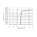
図4は、以上説明した工程により作成したトランジスタのゲート電圧に対するドレイン電流値の測定結果を示すグラフである。図の横軸はゲート電圧[V]、縦軸はドレイン電流[A]を示している。 FIG. 4 is a graph showing a measurement result of a drain current value with respect to a gate voltage of a transistor formed by the above-described steps. The horizontal axis of the figure shows the gate voltage [V], and the vertical axis shows the drain current [A].
グラフより、ゲート電圧が正の値から0付近になると、トランジスタがオフとなり、ドレイン電流が急激に減少することがわかる。ゲート電圧がおおよそ−1Vを下回ると、ドレイン電流値は検出限界を下回り、この測定例では、少なくとも1.0×10⁻¹³[A]以下となる。ゲート電圧をそれ以下の負電圧としても、ドレイン電流が検出されることはなく、オフリーク電流は1.0×10⁻¹³[A]以下を保っている。 From the graph, it can be seen that when the gate voltage becomes closer to 0 from a positive value, the transistor is turned off, and the drain current sharply decreases. When the gate voltage falls below approximately -1 V, the drain current value falls below the detection limit, and in this measurement example, it becomes at least 1.0 × 10 -13 [A] or less. Even if the gate voltage is set to a lower negative voltage, the drain current is not detected, and the off-leak current is kept at 1.0 × 10 -13 [A] or less.
なお、この測定サンプルでは、リーク耐性を測定するためのサンプルとして、ゲート電極の幅を3.5μm、長さを12cm(120,000μm)とした。したがって、同じ幅3.5μmのゲート電極を考えると、電極長さ1mm当たりのオフリーク電流は1.0×10⁻¹⁸[A]以下と極めて小さい値であり、オフリーク電流を十分に小さくすることができている。 In this measurement sample, the width of the gate electrode was 3.5 μm and the length was 12 cm (120,000 μm) as a sample for measuring leak resistance. Therefore, considering a gate electrode having the same width of 3.5 μm, the off-leak current per 1 mm of the electrode length is an extremely small value of 1.0 × 10 −18 [A] or less, and the off-leak current can be sufficiently reduced. I have.
また、窒化シリコンなどの水素を含有する層からの酸化物半導体層への水素の拡散が構造上抑制されているため、トランジスタの特性のばらつきが少なく、均一な特性が得られるとともに、ゲート絶縁層の厚みを過度に厚くする必要がないため、製造工程への負荷も小さい。 In addition, since diffusion of hydrogen from a layer containing hydrogen such as silicon nitride into the oxide semiconductor layer is structurally suppressed, variation in transistor characteristics is small, uniform characteristics are obtained, and the gate insulating layer is formed. Since it is not necessary to make the thickness excessively large, the load on the manufacturing process is small.
すなわち、以上説明した本実施形態に係るトランジスタを使用した表示装置200及び400においては、オフリーク電流が小さく省電力であって、面内において均一な表現性能が得られる。
That is, in the above-described
1 基板、2 アンダーコート層、10 トランジスタ、11 下部ゲート電極層、12 下部ゲート絶縁層、13 酸化物半導体層、14 電極層、15 上部ゲート絶縁層、16 上部ゲート電極層、101 基板、102 アンダーコート層、110 トランジスタ、111 下部ゲート電極層、112 下部ゲート絶縁層、113 酸化物半導体層、114 電極層、115 上部ゲート絶縁層、116 上部ゲート電極層、121 下部第1ゲート絶縁層、122 下部第2ゲート絶縁層、151 上部第1ゲート絶縁層、152 上部第2ゲート絶縁層、200 表示装置、318 平坦化層、319 導電層、321 導電層、322 容量絶縁層、323 画素電極、324 絶縁層、325 有機層、326 対向電極、330 有機EL素子、331 無機絶縁層、332 有機絶縁層、333 無機絶縁層、334 粘着剤、335 対向基板、400 表示装置、418 平坦化層、421 画素電極、422 絶縁層、423 共通電極、424 液晶層、425 オーバーコート層、426 カラーフィルタ、427 対向基板。
Reference Signs List 1 substrate, 2 undercoat layer, 10 transistor, 11 lower gate electrode layer, 12 lower gate insulating layer, 13 oxide semiconductor layer, 14 electrode layer, 15 upper gate insulating layer, 16 upper gate electrode layer, 101 substrate, 102 under Coat layer, 110 transistor, 111 lower gate electrode layer, 112 lower gate insulating layer, 113 oxide semiconductor layer, 114 electrode layer, 115 upper gate insulating layer, 116 upper gate electrode layer, 121 lower first gate insulating layer, 122 lower 2nd gate insulating layer, 151 upper first gate insulating layer, 152 upper second gate insulating layer, 200 display device, 318 planarization layer, 319 conductive layer, 321 conductive layer, 322 capacitive insulating layer, 323 pixel electrode, 324 insulating Layer, 325 organic layer, 326 counter electrode, 330 organic EL element, 331 inorganic insulating layer, 3 2 organic insulating layer, 333 inorganic insulating layer, 334 adhesive, 335 counter substrate, 400 display device, 418 flattening layer, 421 pixel electrode, 422 insulating layer, 423 common electrode, 424 liquid crystal layer, 425 overcoat layer, 426 color Filter, 427 Counter substrate.
Claims (7)
少なくとも1つのゲート電極と、
前記活性層と前記ゲート電極間の前記ゲート電極側に配置された第1ゲート絶縁層と、
前記活性層と前記ゲート電極化の前記活性層側に配置された水素ブロック層である第2ゲート絶縁層と、
を有する薄膜トランジスタ。 An active layer made of an oxide semiconductor containing at least indium and gallium,
At least one gate electrode;
A first gate insulating layer disposed on the gate electrode side between the active layer and the gate electrode;
A second gate insulating layer that is a hydrogen block layer disposed on the active layer side of the active layer and the gate electrode;
A thin film transistor.
請求項1に記載の薄膜トランジスタ。 The thin film transistor according to claim 1, wherein the first gate insulating layer is a silicon nitride layer, the second gate insulating layer is a silicon oxide layer, and the thickness of the second gate insulating layer is thicker than the first gate insulating layer. .
請求項2に記載の薄膜トランジスタ。 The thickness of the first gate insulating layer is 30 nm or more and 400 nm or less, the thickness of the second gate insulating layer is 50 nm or more and 500 nm or less, and the total thickness of the first gate insulating layer and the second gate insulating layer is 400 nm or more,
The thin film transistor according to claim 2.
請求項2又は3に記載の薄膜トランジスタ。 A difference in thickness between the first gate insulating layer and the second gate insulating layer is 50 nm or more;
The thin film transistor according to claim 2.
請求項2〜4のいずれか1項に記載の薄膜トランジスタ。 A total thickness of the first gate insulating layer and the second gate insulating layer is 600 nm or less;
The thin film transistor according to claim 2.
請求項1〜5のいずれか1項に記載の薄膜トランジスタ。 The gate electrode includes a lower gate electrode provided below the active layer, and an upper gate electrode provided above the active layer.
The thin film transistor according to claim 1.
A display device using the thin-film transistor according to claim 1.
Priority Applications (3)
| Application Number | Priority Date | Filing Date | Title |
|---|---|---|---|
| JP2018179131A JP2020053475A (en) | 2018-09-25 | 2018-09-25 | Thin-film transistor and display device |
| PCT/JP2019/030207 WO2020066288A1 (en) | 2018-09-25 | 2019-08-01 | Thin-film transistor and display device |
| US17/199,991 US20210202639A1 (en) | 2018-09-25 | 2021-03-12 | Thin film transistor and display device |
Applications Claiming Priority (1)
| Application Number | Priority Date | Filing Date | Title |
|---|---|---|---|
| JP2018179131A JP2020053475A (en) | 2018-09-25 | 2018-09-25 | Thin-film transistor and display device |
Publications (2)
| Publication Number | Publication Date |
|---|---|
| JP2020053475A true JP2020053475A (en) | 2020-04-02 |
| JP2020053475A5 JP2020053475A5 (en) | 2021-11-04 |
Family
ID=69950583
Family Applications (1)
| Application Number | Title | Priority Date | Filing Date |
|---|---|---|---|
| JP2018179131A Pending JP2020053475A (en) | 2018-09-25 | 2018-09-25 | Thin-film transistor and display device |
Country Status (3)
| Country | Link |
|---|---|
| US (1) | US20210202639A1 (en) |
| JP (1) | JP2020053475A (en) |
| WO (1) | WO2020066288A1 (en) |
Families Citing this family (1)
| Publication number | Priority date | Publication date | Assignee | Title |
|---|---|---|---|---|
| US20210193049A1 (en) * | 2019-12-23 | 2021-06-24 | Apple Inc. | Electronic Display with In-Pixel Compensation and Oxide Drive Transistors |
Citations (3)
| Publication number | Priority date | Publication date | Assignee | Title |
|---|---|---|---|---|
| JP2011054946A (en) * | 2009-08-07 | 2011-03-17 | Semiconductor Energy Lab Co Ltd | Semiconductor device, and method for manufacturing semiconductor device |
| JP2011141524A (en) * | 2009-10-21 | 2011-07-21 | Semiconductor Energy Lab Co Ltd | Display device and electronic device including the same |
| JP2016178279A (en) * | 2014-11-28 | 2016-10-06 | 株式会社半導体エネルギー研究所 | Semiconductor device and display device having semiconductor device |
Family Cites Families (1)
| Publication number | Priority date | Publication date | Assignee | Title |
|---|---|---|---|---|
| JP2019186301A (en) * | 2018-04-04 | 2019-10-24 | 株式会社ジャパンディスプレイ | Display unit |
-
2018
- 2018-09-25 JP JP2018179131A patent/JP2020053475A/en active Pending
-
2019
- 2019-08-01 WO PCT/JP2019/030207 patent/WO2020066288A1/en active Application Filing
-
2021
- 2021-03-12 US US17/199,991 patent/US20210202639A1/en active Pending
Patent Citations (3)
| Publication number | Priority date | Publication date | Assignee | Title |
|---|---|---|---|---|
| JP2011054946A (en) * | 2009-08-07 | 2011-03-17 | Semiconductor Energy Lab Co Ltd | Semiconductor device, and method for manufacturing semiconductor device |
| JP2011141524A (en) * | 2009-10-21 | 2011-07-21 | Semiconductor Energy Lab Co Ltd | Display device and electronic device including the same |
| JP2016178279A (en) * | 2014-11-28 | 2016-10-06 | 株式会社半導体エネルギー研究所 | Semiconductor device and display device having semiconductor device |
Also Published As
| Publication number | Publication date |
|---|---|
| US20210202639A1 (en) | 2021-07-01 |
| WO2020066288A1 (en) | 2020-04-02 |
Similar Documents
| Publication | Publication Date | Title |
|---|---|---|
| US9570621B2 (en) | Display substrate, method of manufacturing the same | |
| US11348948B2 (en) | Manufacturing method of a display device | |
| US8952376B2 (en) | Thin film transistor, and method of manufacturing the same | |
| US9640559B2 (en) | Low temperature poly-silicon array substrate and forming method thereof | |
| US8835929B2 (en) | Pixel structure and thin film transistor | |
| US9214533B2 (en) | Semiconductor device having transparent electrodes | |
| KR20150041511A (en) | Display apparatus and method for manufacturing the same | |
| KR20120042029A (en) | Display device and method for manufacturing the same | |
| JP2018125340A (en) | Display device | |
| KR102067968B1 (en) | Organic Light Emitting Diode Display Device And Manufacturing Method Of The Same | |
| US11791346B2 (en) | Method for manufacturing a display device | |
| TWI451179B (en) | Pixel structure and manufacturing method thereof | |
| KR20170126535A (en) | Thin film transistor array panel | |
| US9595545B2 (en) | Semiconductor device | |
| US9583515B2 (en) | Semiconductor device including substrate which is used in display devices | |
| US20210210524A1 (en) | Thin film transistor and manufacturing method for thin film transistor | |
| KR101604480B1 (en) | Method of fabricating the thin film transistor array substrate using a oxidized semiconductor | |
| US20180233596A1 (en) | Semiconductor device | |
| US20210202639A1 (en) | Thin film transistor and display device | |
| US9305939B2 (en) | Semiconductor device with oxide layer as transparent electrode | |
| US11450721B2 (en) | Array substrate including pixel unit with switching transistor and driving transistor having different threshold voltages for improving display effect, and method of manufacturing the same | |
| KR102468858B1 (en) | Substrate for display and display including the same | |
| KR102659970B1 (en) | Display substrate and method of manufacturing the same | |
| US20230418123A1 (en) | Active matrix substrate and display device | |
| KR20190001279A (en) | Thin Film Transistor Substrate Having High Mobility Semiconductor Material And Method for Manufacturing The Same |
Legal Events
| Date | Code | Title | Description |
|---|---|---|---|
| A521 | Request for written amendment filed |
Free format text: JAPANESE INTERMEDIATE CODE: A523 Effective date: 20210922 |
|
| A621 | Written request for application examination |
Free format text: JAPANESE INTERMEDIATE CODE: A621 Effective date: 20210922 |
|
| A131 | Notification of reasons for refusal |
Free format text: JAPANESE INTERMEDIATE CODE: A131 Effective date: 20220906 |
|
| A02 | Decision of refusal |
Free format text: JAPANESE INTERMEDIATE CODE: A02 Effective date: 20230228 |