JP2020017841A - Voltage-controlled oscillator, pll circuit and cdr device - Google Patents
Voltage-controlled oscillator, pll circuit and cdr device Download PDFInfo
- Publication number
- JP2020017841A JP2020017841A JP2018139140A JP2018139140A JP2020017841A JP 2020017841 A JP2020017841 A JP 2020017841A JP 2018139140 A JP2018139140 A JP 2018139140A JP 2018139140 A JP2018139140 A JP 2018139140A JP 2020017841 A JP2020017841 A JP 2020017841A
- Authority
- JP
- Japan
- Prior art keywords
- circuit
- mos transistor
- node
- controlled oscillator
- capacitance
- Prior art date
- Legal status (The legal status is an assumption and is not a legal conclusion. Google has not performed a legal analysis and makes no representation as to the accuracy of the status listed.)
- Granted
Links
Images


Classifications
-
- H—ELECTRICITY
- H03—ELECTRONIC CIRCUITRY
- H03B—GENERATION OF OSCILLATIONS, DIRECTLY OR BY FREQUENCY-CHANGING, BY CIRCUITS EMPLOYING ACTIVE ELEMENTS WHICH OPERATE IN A NON-SWITCHING MANNER; GENERATION OF NOISE BY SUCH CIRCUITS
- H03B5/00—Generation of oscillations using amplifier with regenerative feedback from output to input
- H03B5/08—Generation of oscillations using amplifier with regenerative feedback from output to input with frequency-determining element comprising lumped inductance and capacitance
- H03B5/12—Generation of oscillations using amplifier with regenerative feedback from output to input with frequency-determining element comprising lumped inductance and capacitance active element in amplifier being semiconductor device
- H03B5/1206—Generation of oscillations using amplifier with regenerative feedback from output to input with frequency-determining element comprising lumped inductance and capacitance active element in amplifier being semiconductor device using multiple transistors for amplification
- H03B5/1212—Generation of oscillations using amplifier with regenerative feedback from output to input with frequency-determining element comprising lumped inductance and capacitance active element in amplifier being semiconductor device using multiple transistors for amplification the amplifier comprising a pair of transistors, wherein an output terminal of each being connected to an input terminal of the other, e.g. a cross coupled pair
- H03B5/1215—Generation of oscillations using amplifier with regenerative feedback from output to input with frequency-determining element comprising lumped inductance and capacitance active element in amplifier being semiconductor device using multiple transistors for amplification the amplifier comprising a pair of transistors, wherein an output terminal of each being connected to an input terminal of the other, e.g. a cross coupled pair the current source or degeneration circuit being in common to both transistors of the pair, e.g. a cross-coupled long-tailed pair
-
- H—ELECTRICITY
- H03—ELECTRONIC CIRCUITRY
- H03L—AUTOMATIC CONTROL, STARTING, SYNCHRONISATION OR STABILISATION OF GENERATORS OF ELECTRONIC OSCILLATIONS OR PULSES
- H03L7/00—Automatic control of frequency or phase; Synchronisation
- H03L7/06—Automatic control of frequency or phase; Synchronisation using a reference signal applied to a frequency- or phase-locked loop
- H03L7/08—Details of the phase-locked loop
- H03L7/085—Details of the phase-locked loop concerning mainly the frequency- or phase-detection arrangement including the filtering or amplification of its output signal
- H03L7/087—Details of the phase-locked loop concerning mainly the frequency- or phase-detection arrangement including the filtering or amplification of its output signal using at least two phase detectors or a frequency and phase detector in the loop
-
- H—ELECTRICITY
- H02—GENERATION; CONVERSION OR DISTRIBUTION OF ELECTRIC POWER
- H02M—APPARATUS FOR CONVERSION BETWEEN AC AND AC, BETWEEN AC AND DC, OR BETWEEN DC AND DC, AND FOR USE WITH MAINS OR SIMILAR POWER SUPPLY SYSTEMS; CONVERSION OF DC OR AC INPUT POWER INTO SURGE OUTPUT POWER; CONTROL OR REGULATION THEREOF
- H02M3/00—Conversion of DC power input into DC power output
- H02M3/02—Conversion of DC power input into DC power output without intermediate conversion into AC
- H02M3/04—Conversion of DC power input into DC power output without intermediate conversion into AC by static converters
- H02M3/06—Conversion of DC power input into DC power output without intermediate conversion into AC by static converters using resistors or capacitors, e.g. potential divider
- H02M3/07—Conversion of DC power input into DC power output without intermediate conversion into AC by static converters using resistors or capacitors, e.g. potential divider using capacitors charged and discharged alternately by semiconductor devices with control electrode, e.g. charge pumps
-
- H—ELECTRICITY
- H03—ELECTRONIC CIRCUITRY
- H03B—GENERATION OF OSCILLATIONS, DIRECTLY OR BY FREQUENCY-CHANGING, BY CIRCUITS EMPLOYING ACTIVE ELEMENTS WHICH OPERATE IN A NON-SWITCHING MANNER; GENERATION OF NOISE BY SUCH CIRCUITS
- H03B5/00—Generation of oscillations using amplifier with regenerative feedback from output to input
- H03B5/02—Details
- H03B5/04—Modifications of generator to compensate for variations in physical values, e.g. power supply, load, temperature
-
- H—ELECTRICITY
- H03—ELECTRONIC CIRCUITRY
- H03B—GENERATION OF OSCILLATIONS, DIRECTLY OR BY FREQUENCY-CHANGING, BY CIRCUITS EMPLOYING ACTIVE ELEMENTS WHICH OPERATE IN A NON-SWITCHING MANNER; GENERATION OF NOISE BY SUCH CIRCUITS
- H03B5/00—Generation of oscillations using amplifier with regenerative feedback from output to input
- H03B5/08—Generation of oscillations using amplifier with regenerative feedback from output to input with frequency-determining element comprising lumped inductance and capacitance
- H03B5/12—Generation of oscillations using amplifier with regenerative feedback from output to input with frequency-determining element comprising lumped inductance and capacitance active element in amplifier being semiconductor device
- H03B5/1206—Generation of oscillations using amplifier with regenerative feedback from output to input with frequency-determining element comprising lumped inductance and capacitance active element in amplifier being semiconductor device using multiple transistors for amplification
- H03B5/1212—Generation of oscillations using amplifier with regenerative feedback from output to input with frequency-determining element comprising lumped inductance and capacitance active element in amplifier being semiconductor device using multiple transistors for amplification the amplifier comprising a pair of transistors, wherein an output terminal of each being connected to an input terminal of the other, e.g. a cross coupled pair
-
- H—ELECTRICITY
- H03—ELECTRONIC CIRCUITRY
- H03B—GENERATION OF OSCILLATIONS, DIRECTLY OR BY FREQUENCY-CHANGING, BY CIRCUITS EMPLOYING ACTIVE ELEMENTS WHICH OPERATE IN A NON-SWITCHING MANNER; GENERATION OF NOISE BY SUCH CIRCUITS
- H03B5/00—Generation of oscillations using amplifier with regenerative feedback from output to input
- H03B5/08—Generation of oscillations using amplifier with regenerative feedback from output to input with frequency-determining element comprising lumped inductance and capacitance
- H03B5/12—Generation of oscillations using amplifier with regenerative feedback from output to input with frequency-determining element comprising lumped inductance and capacitance active element in amplifier being semiconductor device
- H03B5/1228—Generation of oscillations using amplifier with regenerative feedback from output to input with frequency-determining element comprising lumped inductance and capacitance active element in amplifier being semiconductor device the amplifier comprising one or more field effect transistors
-
- H—ELECTRICITY
- H03—ELECTRONIC CIRCUITRY
- H03B—GENERATION OF OSCILLATIONS, DIRECTLY OR BY FREQUENCY-CHANGING, BY CIRCUITS EMPLOYING ACTIVE ELEMENTS WHICH OPERATE IN A NON-SWITCHING MANNER; GENERATION OF NOISE BY SUCH CIRCUITS
- H03B5/00—Generation of oscillations using amplifier with regenerative feedback from output to input
- H03B5/08—Generation of oscillations using amplifier with regenerative feedback from output to input with frequency-determining element comprising lumped inductance and capacitance
- H03B5/12—Generation of oscillations using amplifier with regenerative feedback from output to input with frequency-determining element comprising lumped inductance and capacitance active element in amplifier being semiconductor device
- H03B5/1237—Generation of oscillations using amplifier with regenerative feedback from output to input with frequency-determining element comprising lumped inductance and capacitance active element in amplifier being semiconductor device comprising means for varying the frequency of the generator
- H03B5/124—Generation of oscillations using amplifier with regenerative feedback from output to input with frequency-determining element comprising lumped inductance and capacitance active element in amplifier being semiconductor device comprising means for varying the frequency of the generator the means comprising a voltage dependent capacitance
- H03B5/1243—Generation of oscillations using amplifier with regenerative feedback from output to input with frequency-determining element comprising lumped inductance and capacitance active element in amplifier being semiconductor device comprising means for varying the frequency of the generator the means comprising a voltage dependent capacitance the means comprising voltage variable capacitance diodes
-
- H—ELECTRICITY
- H03—ELECTRONIC CIRCUITRY
- H03B—GENERATION OF OSCILLATIONS, DIRECTLY OR BY FREQUENCY-CHANGING, BY CIRCUITS EMPLOYING ACTIVE ELEMENTS WHICH OPERATE IN A NON-SWITCHING MANNER; GENERATION OF NOISE BY SUCH CIRCUITS
- H03B5/00—Generation of oscillations using amplifier with regenerative feedback from output to input
- H03B5/08—Generation of oscillations using amplifier with regenerative feedback from output to input with frequency-determining element comprising lumped inductance and capacitance
- H03B5/12—Generation of oscillations using amplifier with regenerative feedback from output to input with frequency-determining element comprising lumped inductance and capacitance active element in amplifier being semiconductor device
- H03B5/1237—Generation of oscillations using amplifier with regenerative feedback from output to input with frequency-determining element comprising lumped inductance and capacitance active element in amplifier being semiconductor device comprising means for varying the frequency of the generator
- H03B5/124—Generation of oscillations using amplifier with regenerative feedback from output to input with frequency-determining element comprising lumped inductance and capacitance active element in amplifier being semiconductor device comprising means for varying the frequency of the generator the means comprising a voltage dependent capacitance
- H03B5/1246—Generation of oscillations using amplifier with regenerative feedback from output to input with frequency-determining element comprising lumped inductance and capacitance active element in amplifier being semiconductor device comprising means for varying the frequency of the generator the means comprising a voltage dependent capacitance the means comprising transistors used to provide a variable capacitance
- H03B5/1253—Generation of oscillations using amplifier with regenerative feedback from output to input with frequency-determining element comprising lumped inductance and capacitance active element in amplifier being semiconductor device comprising means for varying the frequency of the generator the means comprising a voltage dependent capacitance the means comprising transistors used to provide a variable capacitance the transistors being field-effect transistors
-
- H—ELECTRICITY
- H03—ELECTRONIC CIRCUITRY
- H03B—GENERATION OF OSCILLATIONS, DIRECTLY OR BY FREQUENCY-CHANGING, BY CIRCUITS EMPLOYING ACTIVE ELEMENTS WHICH OPERATE IN A NON-SWITCHING MANNER; GENERATION OF NOISE BY SUCH CIRCUITS
- H03B5/00—Generation of oscillations using amplifier with regenerative feedback from output to input
- H03B5/08—Generation of oscillations using amplifier with regenerative feedback from output to input with frequency-determining element comprising lumped inductance and capacitance
- H03B5/12—Generation of oscillations using amplifier with regenerative feedback from output to input with frequency-determining element comprising lumped inductance and capacitance active element in amplifier being semiconductor device
- H03B5/1237—Generation of oscillations using amplifier with regenerative feedback from output to input with frequency-determining element comprising lumped inductance and capacitance active element in amplifier being semiconductor device comprising means for varying the frequency of the generator
- H03B5/1262—Generation of oscillations using amplifier with regenerative feedback from output to input with frequency-determining element comprising lumped inductance and capacitance active element in amplifier being semiconductor device comprising means for varying the frequency of the generator the means comprising switched elements
- H03B5/1265—Generation of oscillations using amplifier with regenerative feedback from output to input with frequency-determining element comprising lumped inductance and capacitance active element in amplifier being semiconductor device comprising means for varying the frequency of the generator the means comprising switched elements switched capacitors
-
- H—ELECTRICITY
- H03—ELECTRONIC CIRCUITRY
- H03B—GENERATION OF OSCILLATIONS, DIRECTLY OR BY FREQUENCY-CHANGING, BY CIRCUITS EMPLOYING ACTIVE ELEMENTS WHICH OPERATE IN A NON-SWITCHING MANNER; GENERATION OF NOISE BY SUCH CIRCUITS
- H03B5/00—Generation of oscillations using amplifier with regenerative feedback from output to input
- H03B5/20—Generation of oscillations using amplifier with regenerative feedback from output to input with frequency-determining element comprising resistance and either capacitance or inductance, e.g. phase-shift oscillator
- H03B5/24—Generation of oscillations using amplifier with regenerative feedback from output to input with frequency-determining element comprising resistance and either capacitance or inductance, e.g. phase-shift oscillator active element in amplifier being semiconductor device
-
- H—ELECTRICITY
- H03—ELECTRONIC CIRCUITRY
- H03L—AUTOMATIC CONTROL, STARTING, SYNCHRONISATION OR STABILISATION OF GENERATORS OF ELECTRONIC OSCILLATIONS OR PULSES
- H03L7/00—Automatic control of frequency or phase; Synchronisation
- H03L7/06—Automatic control of frequency or phase; Synchronisation using a reference signal applied to a frequency- or phase-locked loop
- H03L7/08—Details of the phase-locked loop
- H03L7/0807—Details of the phase-locked loop concerning mainly a recovery circuit for the reference signal
-
- H—ELECTRICITY
- H03—ELECTRONIC CIRCUITRY
- H03L—AUTOMATIC CONTROL, STARTING, SYNCHRONISATION OR STABILISATION OF GENERATORS OF ELECTRONIC OSCILLATIONS OR PULSES
- H03L7/00—Automatic control of frequency or phase; Synchronisation
- H03L7/06—Automatic control of frequency or phase; Synchronisation using a reference signal applied to a frequency- or phase-locked loop
- H03L7/08—Details of the phase-locked loop
- H03L7/085—Details of the phase-locked loop concerning mainly the frequency- or phase-detection arrangement including the filtering or amplification of its output signal
- H03L7/093—Details of the phase-locked loop concerning mainly the frequency- or phase-detection arrangement including the filtering or amplification of its output signal using special filtering or amplification characteristics in the loop
-
- H—ELECTRICITY
- H03—ELECTRONIC CIRCUITRY
- H03L—AUTOMATIC CONTROL, STARTING, SYNCHRONISATION OR STABILISATION OF GENERATORS OF ELECTRONIC OSCILLATIONS OR PULSES
- H03L7/00—Automatic control of frequency or phase; Synchronisation
- H03L7/06—Automatic control of frequency or phase; Synchronisation using a reference signal applied to a frequency- or phase-locked loop
- H03L7/08—Details of the phase-locked loop
- H03L7/099—Details of the phase-locked loop concerning mainly the controlled oscillator of the loop
-
- H—ELECTRICITY
- H04—ELECTRIC COMMUNICATION TECHNIQUE
- H04L—TRANSMISSION OF DIGITAL INFORMATION, e.g. TELEGRAPHIC COMMUNICATION
- H04L7/00—Arrangements for synchronising receiver with transmitter
- H04L7/02—Speed or phase control by the received code signals, the signals containing no special synchronisation information
- H04L7/033—Speed or phase control by the received code signals, the signals containing no special synchronisation information using the transitions of the received signal to control the phase of the synchronising-signal-generating means, e.g. using a phase-locked loop
- H04L7/0331—Speed or phase control by the received code signals, the signals containing no special synchronisation information using the transitions of the received signal to control the phase of the synchronising-signal-generating means, e.g. using a phase-locked loop with a digital phase-locked loop [PLL] processing binary samples, e.g. add/subtract logic for correction of receiver clock
-
- H—ELECTRICITY
- H03—ELECTRONIC CIRCUITRY
- H03B—GENERATION OF OSCILLATIONS, DIRECTLY OR BY FREQUENCY-CHANGING, BY CIRCUITS EMPLOYING ACTIVE ELEMENTS WHICH OPERATE IN A NON-SWITCHING MANNER; GENERATION OF NOISE BY SUCH CIRCUITS
- H03B2201/00—Aspects of oscillators relating to varying the frequency of the oscillations
- H03B2201/02—Varying the frequency of the oscillations by electronic means
- H03B2201/0208—Varying the frequency of the oscillations by electronic means the means being an element with a variable capacitance, e.g. capacitance diode
-
- H—ELECTRICITY
- H04—ELECTRIC COMMUNICATION TECHNIQUE
- H04L—TRANSMISSION OF DIGITAL INFORMATION, e.g. TELEGRAPHIC COMMUNICATION
- H04L7/00—Arrangements for synchronising receiver with transmitter
- H04L7/02—Speed or phase control by the received code signals, the signals containing no special synchronisation information
- H04L7/033—Speed or phase control by the received code signals, the signals containing no special synchronisation information using the transitions of the received signal to control the phase of the synchronising-signal-generating means, e.g. using a phase-locked loop
Landscapes
- Engineering & Computer Science (AREA)
- Power Engineering (AREA)
- Computer Networks & Wireless Communication (AREA)
- Signal Processing (AREA)
- Inductance-Capacitance Distribution Constants And Capacitance-Resistance Oscillators (AREA)
- Stabilization Of Oscillater, Synchronisation, Frequency Synthesizers (AREA)
Abstract
【課題】可変容量素子のリーク電流による性能悪化を抑制することができる電圧制御発振器を提供する。【解決手段】電圧制御発振器40Aは、第1容量回路41A、第2容量回路42A、第3容量回路43、インダクタ44,45およびNMOSトランジスタ46,47を備える。第1容量回路41Aおよび第2容量回路42Aそれぞれは、可変容量素子C1、容量素子C2、検出回路48および補償回路49を含む。可変容量素子C1は、ノードN1とノードN2との間に設けられている。可変容量素子C1の容量値は、ノードN1とノードN2との間の電圧値に依存する。検出回路48は、ノードN2にバイアス電圧値Vbiasを与えるとともに、可変容量素子C1に流れるリーク電流の量を検出する。補償回路49は、検出回路48による検出結果に基づいて、可変容量素子C1のリーク電流を補償する電流をノードN1に流す。【選択図】図5Provided is a voltage controlled oscillator that can suppress performance deterioration due to leakage current of a variable capacitance element. A voltage controlled oscillator includes a first capacitance circuit, a second capacitance circuit, a third capacitance circuit, inductors, and NMOS transistors. Each of the first capacitance circuit 41A and the second capacitance circuit 42A includes a variable capacitance element C1, a capacitance element C2, a detection circuit 48, and a compensation circuit 49. The variable capacitance element C1 is provided between the node N1 and the node N2. The capacitance value of the variable capacitance element C1 depends on the voltage value between the nodes N1 and N2. The detection circuit 48 supplies the bias voltage Vbias to the node N2 and detects the amount of leak current flowing through the variable capacitance element C1. The compensating circuit 49 supplies a current for compensating for a leak current of the variable capacitance element C1 to the node N1 based on the detection result of the detecting circuit 48. [Selection diagram] FIG.
Description
本発明は、電圧制御発振器、PLL回路およびCDR装置に関するものである。 The present invention relates to a voltage controlled oscillator, a PLL circuit, and a CDR device.
電圧制御発振器(VCO: Voltage Controlled Oscillator)は、入力される制御電圧値に応じた周波数を有する発振信号を出力することができる。電圧制御発振器は、PLL(Phase Locked Loop)回路およびCDR(Clock Data Recovery)装置等において重要な一構成要素として用いられる。電圧制御発振器としては様々なタイプのものがある。そのなかでも、LC-VCOは、インダクタおよび電圧制御によって容量値が変化するキャパシタを含み、これらインダクタおよびキャパシタによる共振現象により、入力される制御電圧値に応じた周波数を有する発振信号を出力する。他のタイプの電圧制御発振器と比較すると、LC-VCOのジッタは少ない。したがって、10Gbps以上の周波数の場合には、様々なタイプがある電圧制御発振器のなかでもLC-VCOの使用が不可欠である。 A voltage controlled oscillator (VCO) can output an oscillation signal having a frequency corresponding to an input control voltage value. The voltage controlled oscillator is used as an important component in a PLL (Phase Locked Loop) circuit, a CDR (Clock Data Recovery) device, and the like. There are various types of voltage controlled oscillators. Among them, the LC-VCO includes an inductor and a capacitor whose capacitance value changes by voltage control, and outputs an oscillation signal having a frequency corresponding to an input control voltage value by a resonance phenomenon of the inductor and the capacitor. Compared to other types of voltage controlled oscillators, the LC-VCO has less jitter. Therefore, in the case of a frequency of 10 Gbps or more, use of the LC-VCO is indispensable among various types of voltage controlled oscillators.
LC-VCOは、共振現象に関与するキャパシタとして、2端子間に印加される電圧値によって容量値が変化する容量素子を含む。このような容量素子は、バリキャップ(Varicap Diode)、バラクタ(Varactor Diode)または可変容量ダイオード(Variable Capacitance Diode)と呼ばれている。本明細書では、このような容量素子を「可変容量素子」という。例えば、可変容量素子は、CMOSプロセスにより低濃度N型不純物を注入したNウェルに高濃度P型不純物を注入したP+領域を有するダイオードにより構成される。また、例えば、可変容量素子は、低濃度P型不純物を注入したPウェルに高濃度N型不純物を注入した2つのN+領域を有するMOSトランジスタにより構成される。 The LC-VCO includes, as a capacitor involved in the resonance phenomenon, a capacitance element whose capacitance value changes according to a voltage value applied between two terminals. Such a capacitance element is called a varicap (Varicap Diode), a varactor (Varactor Diode), or a variable capacitance diode (Variable Capacitance Diode). In this specification, such a capacitor is referred to as a “variable capacitor”. For example, the variable capacitance element is configured by a diode having a P + region in which a high-concentration P-type impurity is implanted in an N-well in which a low-concentration N-type impurity is implanted by a CMOS process. Further, for example, the variable capacitance element is configured by a MOS transistor having two N + regions in which a high concentration N-type impurity is implanted in a P well in which a low concentration P-type impurity is implanted.
一般に、可変容量素子は、印加される電圧値に応じた容量値を有するだけでなく、該電圧値に応じた量のリーク電流が生じる。可変容量素子のリーク電流により、LC-VCOから出力される発振信号にジッタが生じて、LC-VCOの性能が悪くなる場合がある。LC-VCOの性能が悪いと、これを用いるPLL回路またはCDR装置の性能も悪くなる。 In general, a variable capacitance element has not only a capacitance value according to an applied voltage value but also an amount of leakage current according to the voltage value. Oscillation signals output from the LC-VCO may cause jitter due to leakage current of the variable capacitance element, and the performance of the LC-VCO may deteriorate. When the performance of the LC-VCO is poor, the performance of the PLL circuit or CDR device using the same is also poor.
このような問題を解消することを意図した発明が特許文献1に開示されている。この文献に開示された発明は、LC-VCOとは別にレプリカ回路を備える。レプリカ回路は、LC-VCOの可変容量素子と同等の可変容量素子を含み、また、差動アンプおよびカレントミラー回路をも含む。そして、この発明は、レプリカ回路の可変容量素子のリーク電流によりLC-VCOの可変容量素子のリーク電流を補償することにより、LC-VCOの性能悪化を抑制することを図る。
しかし、特許文献1に開示された発明では、LC-VCOの可変容量素子とレプリカ回路の可変容量素子との間で特性が相違していると、各々の可変容量素子に流れるリーク電流が相違し、十分に補償をすることができない。それ故、LC-VCOの性能悪化を十分に抑制することができず、また、これを用いるPLL回路またはCDR装置の性能悪化を十分に抑制することもできない。また、特許文献1に開示された発明では、半導体基板上に集積化する場合にレプリカ回路の可変容量素子のレイアウト面積が大きい。
However, in the invention disclosed in
本発明は、上記問題点を解消する為になされたものであり、可変容量素子のリーク電流による性能悪化を抑制することができ、レイアウト面積の増加を抑制することができる電圧制御発振器を提供することを目的とする。また、本発明は、LC-VCOの可変容量素子のリーク電流による性能悪化を抑制することができるPLL回路およびCDR装置を提供することを目的とする。 The present invention has been made to solve the above problems, and provides a voltage controlled oscillator that can suppress performance deterioration due to leakage current of a variable capacitance element and can suppress an increase in layout area. The purpose is to: It is another object of the present invention to provide a PLL circuit and a CDR device that can suppress performance deterioration due to leakage current of a variable capacitance element of an LC-VCO.
本発明の電圧制御発振器は、インダクタ、第1容量回路および第2容量回路を備え、これらインダクタ、第1容量回路および第2容量回路による共振現象により、入力される制御電圧値に応じた周波数を有する発振信号を出力する。本発明の電圧制御発振器において、第1容量回路および第2容量回路それぞれは、ノードN1とノードN2との間に設けられ両ノード間の電圧値に応じた容量値を有する可変容量素子と、ノードN2とノードN3との間に設けられた容量素子と、ノードN2にバイアス電圧値を与えるとともに可変容量素子に流れるリーク電流の量を検出する検出回路と、検出回路による検出結果に基づいてリーク電流を補償する電流をノードN1に流す補償回路と、を備える。さらに、本発明の電圧制御発振器において、第1容量回路および第2容量回路それぞれのノードN3の間にインダクタが設けられており、第1容量回路および第2容量回路それぞれのノードN1は互いに電気的に接続されて制御電圧値が入力される。 A voltage controlled oscillator according to the present invention includes an inductor, a first capacitance circuit, and a second capacitance circuit, and a frequency corresponding to an input control voltage value is set by a resonance phenomenon of the inductor, the first capacitance circuit, and the second capacitance circuit. Output an oscillation signal. In the voltage controlled oscillator according to the present invention, each of the first capacitance circuit and the second capacitance circuit is provided between the node N1 and the node N2, and has a variable capacitance element having a capacitance value according to a voltage value between the two nodes; A capacitance element provided between N2 and node N3, a detection circuit for applying a bias voltage value to node N2 and detecting the amount of leakage current flowing through the variable capacitance element, and a leakage current based on a detection result by the detection circuit And a compensating circuit that supplies a current for compensating the above to the node N1. Further, in the voltage controlled oscillator of the present invention, an inductor is provided between the node N3 of each of the first capacitance circuit and the second capacitance circuit, and the node N1 of each of the first capacitance circuit and the second capacitance circuit is electrically connected to each other. And a control voltage value is input.
本発明の電圧制御発振器は、第1容量回路および第2容量回路それぞれのノードN3に接続され、制御信号により設定される容量値を有する第3容量回路を更に備えるのが好適である。 It is preferable that the voltage controlled oscillator of the present invention further includes a third capacitance circuit connected to the node N3 of each of the first capacitance circuit and the second capacitance circuit and having a capacitance value set by a control signal.
本発明の電圧制御発振器において、第1容量回路および第2容量回路それぞれの検出回路が共通であるのが好適であり、第1容量回路および第2容量回路それぞれの補償回路が共通であるのも好適である。 In the voltage controlled oscillator of the present invention, it is preferable that the first capacitance circuit and the second capacitance circuit have a common detection circuit, and that the first capacitance circuit and the second capacitance circuit have a common compensation circuit. It is suitable.
本発明の電圧制御発振器において、検出回路は、(1) 第1電位供給端にソースが接続されたMOSトランジスタM1と、(2) MOSトランジスタM1のドレインとノードN2との間に設けられた抵抗部と、(3) MOSトランジスタM1のドレインに接続された第1入力端子と、バイアス電圧値が入力される第2入力端子と、MOSトランジスタM1のゲートに接続された出力端子とを有する差動アンプと、を含むのが好適である。また、補償回路は、(1) 第1電位供給端にソースが接続され、差動アンプの出力端子にゲートが接続されたMOSトランジスタM2と、(2) 第2電位供給端とMOSトランジスタM2のドレインとの間に設けられたMOSトランジスタM3と、(3) 第2電位供給端とノードN1との間に設けられ、MOSトランジスタM3とともにカレントミラー回路を構成し、MOSトランジスタM3に流れる電流と同じ量の電流を流すMOSトランジスタM4と、を含むのが好適である。 In the voltage controlled oscillator of the present invention, the detection circuit includes: (1) a MOS transistor M1 having a source connected to the first potential supply terminal; and (2) a resistor provided between the drain of the MOS transistor M1 and the node N2. And (3) a differential having a first input terminal connected to the drain of the MOS transistor M1, a second input terminal to which a bias voltage value is input, and an output terminal connected to the gate of the MOS transistor M1. And an amplifier. The compensation circuit includes: (1) a MOS transistor M2 having a source connected to the first potential supply terminal and a gate connected to the output terminal of the differential amplifier; and (2) a MOS transistor M2 having the second potential supply terminal and the MOS transistor M2. A MOS transistor M3 provided between the MOS transistor M3 and the drain; and (3) a current mirror circuit provided between the second potential supply terminal and the node N1 to form a current mirror circuit together with the MOS transistor M3. And a MOS transistor M4 for flowing an amount of current.
なお、第1電位供給端および第2電位供給端のうち、一方は高電位供給端であり、他方は低電位供給端である。第1電位供給端が高電位供給端であって第2電位供給端が低電位供給端である場合、高電位供給端にソースが接続されるMOSトランジスタM1,M2はPMOSトランジスタであり、低電位供給端にソースが接続されるMOSトランジスタM3,M4はNMOSトランジスタである。逆に、第1電位供給端が低電位供給端であって第2電位供給端が高電位供給端である場合、低電位供給端にソースが接続されるMOSトランジスタM1,M2はNMOSトランジスタであり、高電位供給端にソースが接続されるMOSトランジスタM3,M4はPMOSトランジスタである。 One of the first potential supply terminal and the second potential supply terminal is a high potential supply terminal, and the other is a low potential supply terminal. When the first potential supply terminal is a high potential supply terminal and the second potential supply terminal is a low potential supply terminal, the MOS transistors M1 and M2 whose sources are connected to the high potential supply terminal are PMOS transistors, and The MOS transistors M3 and M4 whose sources are connected to the supply terminals are NMOS transistors. Conversely, when the first potential supply terminal is a low potential supply terminal and the second potential supply terminal is a high potential supply terminal, the MOS transistors M1 and M2 whose sources are connected to the low potential supply terminal are NMOS transistors. And the MOS transistors M3 and M4 whose sources are connected to the high potential supply terminals are PMOS transistors.
本発明の電圧制御発振器において、検出回路は、第2電位供給端とMOSトランジスタM1のドレインとの間に設けられた第1電流源を更に含むのが好適である。また、検出回路は、第2電位供給端とノードN2との間に設けられた第2電流源を更に含むのも好適である。 In the voltage controlled oscillator according to the present invention, it is preferable that the detection circuit further includes a first current source provided between the second potential supply terminal and the drain of the MOS transistor M1. Preferably, the detection circuit further includes a second current source provided between the second potential supply terminal and the node N2.
本発明の電圧制御発振器において、補償回路は、第1電位供給端とノードN1との間に設けられた第3電流源を更に含むのが好適である。また、補償回路は、第2電位供給端とMOSトランジスタM3およびMOSトランジスタM4それぞれのゲートとの間に設けられた第4電流源を更に含むのも好適である。 In the voltage controlled oscillator of the present invention, it is preferable that the compensation circuit further includes a third current source provided between the first potential supply terminal and the node N1. It is also preferable that the compensation circuit further includes a fourth current source provided between the second potential supply terminal and the gates of the MOS transistor M3 and the MOS transistor M4.
本発明の電圧制御発振器において、検出回路は、(1) 第1電位供給端にソースが接続されたMOSトランジスタM11と、(2) 第2電位供給端にソースが接続されたMOSトランジスタM21と、(3) MOSトランジスタM11およびMOSトランジスタM21それぞれのドレインとノードN2との間に設けられた抵抗部と、(4) MOSトランジスタM11およびMOSトランジスタM21それぞれのドレインに接続された第1入力端子と、バイアス電圧値が入力される第2入力端子と、MOSトランジスタM11およびMOSトランジスタM21それぞれのゲートに接続された出力端子とを有する差動アンプと、を含むのが好適である。また、補償回路は、(1) 第1電位供給端にソースが接続され、差動アンプの出力端子にゲートが接続されたMOSトランジスタM12と、(2) 第2電位供給端とMOSトランジスタM12のドレインとの間に設けられたMOSトランジスタM13と、(3) 第2電位供給端とノードN1との間に設けられ、MOSトランジスタM13とともにカレントミラー回路を構成し、MOSトランジスタM13に流れる電流と同じ量の電流を流すMOSトランジスタM14と、(4) 第2電位供給端にソースが接続され、差動アンプの出力端子にゲートが接続されたMOSトランジスタM22と、(5) 第1電位供給端とMOSトランジスタM22のドレインとの間に設けられたMOSトランジスタM23と、(6) 第1電位供給端とノードN1との間に設けられ、MOSトランジスタM23とともにカレントミラー回路を構成し、MOSトランジスタM23に流れる電流と同じ量の電流を流すMOSトランジスタM24と、を含むのが好適である。 In the voltage controlled oscillator of the present invention, the detection circuit includes: (1) a MOS transistor M11 having a source connected to the first potential supply terminal; and (2) a MOS transistor M21 having a source connected to the second potential supply terminal. (3) a resistor provided between the drain of each of the MOS transistors M11 and M21 and the node N2; (4) a first input terminal connected to the drain of each of the MOS transistors M11 and M21; It is preferable to include a differential amplifier having a second input terminal to which a bias voltage value is input, and an output terminal connected to the gate of each of the MOS transistor M11 and the MOS transistor M21. The compensation circuit includes: (1) a MOS transistor M12 having a source connected to the first potential supply terminal and a gate connected to the output terminal of the differential amplifier; and (2) a MOS transistor M12 having the second potential supply terminal and the MOS transistor M12. A MOS transistor M13 provided between the MOS transistor M13 and the drain; and (3) a current mirror circuit provided between the second potential supply terminal and the node N1 to form a current mirror circuit together with the MOS transistor M13. (4) a MOS transistor M22 having a source connected to the second potential supply terminal and a gate connected to the output terminal of the differential amplifier, and (5) a first potential supply terminal. A MOS transistor M23 provided between the drain of the MOS transistor M22 and (6) a MOS transistor M23 provided between the first potential supply terminal and the node N1; The transistor M23 constitute a current mirror circuit, the MOS transistors M24 to flow the same amount of current as the current flowing through the MOS transistor M23, which preferably includes a.
なお、第1電位供給端および第2電位供給端のうち、一方は高電位供給端であり、他方は低電位供給端である。第1電位供給端が高電位供給端であって第2電位供給端が低電位供給端である場合、高電位供給端にソースが接続されるMOSトランジスタM11,M12,M23,M24はPMOSトランジスタであり、低電位供給端にソースが接続されるMOSトランジスタM21,M22,M13,M14はNMOSトランジスタである。逆に、第1電位供給端が低電位供給端であって第2電位供給端が高電位供給端である場合、低電位供給端にソースが接続されるMOSトランジスタM11,M12,M23,M24はNMOSトランジスタであり、高電位供給端にソースが接続されるMOSトランジスタM21,M22,M13,M14はPMOSトランジスタである。また、差動アンプの第1入力端子および第2入力端子のうち、一方は反転入力端子であり、他方は非反転入力端子である。 One of the first potential supply terminal and the second potential supply terminal is a high potential supply terminal, and the other is a low potential supply terminal. When the first potential supply terminal is a high potential supply terminal and the second potential supply terminal is a low potential supply terminal, the MOS transistors M11, M12, M23, and M24 whose sources are connected to the high potential supply terminal are PMOS transistors. The MOS transistors M21, M22, M13, M14 whose sources are connected to the low potential supply terminals are NMOS transistors. Conversely, when the first potential supply terminal is the low potential supply terminal and the second potential supply terminal is the high potential supply terminal, the MOS transistors M11, M12, M23, and M24 whose sources are connected to the low potential supply terminal are The MOS transistors M21, M22, M13 and M14, which are NMOS transistors and whose sources are connected to the high potential supply terminals, are PMOS transistors. One of the first input terminal and the second input terminal of the differential amplifier is an inverting input terminal, and the other is a non-inverting input terminal.
本発明の電圧制御発振器において、検出回路は、抵抗部として、ゲート電圧に応じた抵抗値を有するMOSトランジスタM5を含むのが好適である。 In the voltage controlled oscillator according to the present invention, it is preferable that the detection circuit includes, as the resistance unit, a MOS transistor M5 having a resistance value according to a gate voltage.
本発明のPLL回路は、(1) 入力される制御電圧値に応じた周波数を有する発振信号を出力する上記の本発明の電圧制御発振器と、(2) 電圧制御発振器から出力される発振信号または該発振信号を分周した信号を帰還発振信号として入力するとともに、入力信号をも入力し、これら帰還発振信号と入力信号との間の位相差を検出して、この位相差を表す位相差信号を出力する位相比較器と、(3) 位相比較器から出力される位相差信号を入力して、この位相差信号が表す位相差に応じた充放電電流を出力するチャージポンプと、(4) チャージポンプから出力される充放電電流を入力し、この充放電量に応じて増減される制御電圧値を電圧制御発振器へ出力するループフィルタと、を備える。 The PLL circuit of the present invention includes: (1) the above-described voltage-controlled oscillator that outputs an oscillation signal having a frequency corresponding to the input control voltage value; and (2) the oscillation signal output from the voltage-controlled oscillator. A signal obtained by dividing the oscillation signal is input as a feedback oscillation signal, an input signal is also input, a phase difference between the feedback oscillation signal and the input signal is detected, and a phase difference signal representing the phase difference is detected. And (3) a charge pump that receives the phase difference signal output from the phase comparator and outputs a charge / discharge current corresponding to the phase difference represented by the phase difference signal, and (4) A loop filter that receives a charge / discharge current output from the charge pump and outputs a control voltage value that is increased or decreased according to the charge / discharge amount to a voltage-controlled oscillator.
本発明のPLL回路は、電圧制御発振器として複数の電圧制御発振器を備え、複数の電圧制御発振器のうち何れか1つの電圧制御発振器から出力される発振信号を選択して出力する選択部を更に備えるのが好適である。 The PLL circuit of the present invention includes a plurality of voltage-controlled oscillators as voltage-controlled oscillators, and further includes a selection unit that selects and outputs an oscillation signal output from any one of the plurality of voltage-controlled oscillators. Is preferred.
本発明のPLL回路において、複数の電圧制御発振器のうち選択部により選択された電圧制御発振器を除く他の電圧制御発振器は、バイアス電圧値に替えて制御電圧値を入力するのが好適である。 In the PLL circuit of the present invention, it is preferable that a voltage controlled oscillator other than the voltage controlled oscillator selected by the selection unit among the plurality of voltage controlled oscillators receives a control voltage value instead of the bias voltage value.
本発明のCDR装置は、クロックが埋め込まれたデジタル信号を入力し、このデジタル信号に基づいてデータおよびクロックを復元して、その復元データおよび復元クロックを出力する。本発明のCDR装置は、(1) 復元クロックが指示するタイミングでデジタル信号のデータをサンプリングして、そのサンプリングしたデータを復元データとして復元クロックに同期して出力するサンプラと、(2) 入力信号として復元データを位相比較器に入力し、電圧制御発振器から発振信号として復元クロックを出力するともに、復元クロックをサンプラに与える上記の本発明のPLL回路と、を備える。 The CDR device of the present invention receives a digital signal in which a clock is embedded, restores data and a clock based on the digital signal, and outputs the restored data and the restored clock. The CDR device according to the present invention includes: (1) a sampler that samples digital signal data at a timing indicated by a restored clock, and outputs the sampled data as restored data in synchronization with the restored clock; And the PLL circuit of the present invention for supplying a restored clock to a sampler while inputting restored data to a phase comparator, outputting a restored clock as an oscillation signal from a voltage controlled oscillator.
本発明の容量回路は、ノードN1とノードN2との間に設けられ両ノード間の電圧値に応じた容量値を有する可変容量素子と、ノードN2とノードN3との間に設けられた容量素子と、ノードN2にバイアス電圧値を与えるとともに可変容量素子に流れるリーク電流の量を検出する検出回路と、検出回路による検出結果に基づいてリーク電流を補償する電流をノードN1に流す補償回路と、を備える。 A capacitance circuit according to the present invention includes a variable capacitance element provided between a node N1 and a node N2 and having a capacitance value according to a voltage value between the two nodes, and a capacitance element provided between a node N2 and a node N3. A detection circuit for applying a bias voltage value to the node N2 and detecting an amount of leakage current flowing through the variable capacitance element; a compensation circuit for flowing a current for compensating the leakage current to the node N1 based on a detection result by the detection circuit; Is provided.
本発明のLC-VCOは、可変容量素子のリーク電流による性能悪化を抑制することができ、レイアウト面積の増加を抑制することができる。 The LC-VCO of the present invention can suppress the performance deterioration due to the leak current of the variable capacitance element, and can suppress the increase in the layout area.
以下、添付図面を参照して、本発明を実施するための形態を詳細に説明する。なお、図面の説明において同一の要素には同一の符号を付し、重複する説明を省略する。本発明は、これらの例示に限定されるものではなく、特許請求の範囲によって示され、特許請求の範囲と均等の意味および範囲内でのすべての変更が含まれることが意図される。 Hereinafter, embodiments for carrying out the present invention will be described in detail with reference to the accompanying drawings. In the description of the drawings, the same elements will be denoted by the same reference symbols, without redundant description. The present invention is not limited to these exemplifications, but is indicated by the claims, and is intended to include any modifications within the scope and meaning equivalent to the claims.
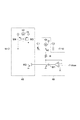
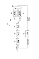
図1は、PLL回路1の構成を示す図である。PLL回路1は、位相比較器10、チャージポンプ20、ループフィルタ30、電圧制御発振器40および分周器50を備える。ループフィルタ30は、抵抗器31、容量素子32および容量素子33を含む。
FIG. 1 is a diagram showing a configuration of the
位相比較器10は、分周器50から出力される帰還発振信号を入力するとともに、入力信号をも入力する。入力信号は、周波数が一定である基準発振信号であってもよいし、各ビットの期間が一定であるデジタル信号であってもよい。位相比較器10は、これら帰還発振信号と入力信号との間の位相差を検出して、この位相差を表す位相差信号をチャージポンプ20へ出力する。位相差信号は、帰還発振信号および入力信号のうち何れの信号の位相が進んでいるかを表す。
The
チャージポンプ20は、位相比較器10から出力される位相差信号を入力して、この位相差信号が表す位相差に応じた充放電電流をループフィルタ30へ出力する。チャージポンプ20からループフィルタ30へ出力される充放電電流は、基準発振信号および入力信号のうち何れの信号の位相が進んでいるかに応じて極性が異なる。ループフィルタ30は、チャージポンプ20から出力される充放電電流を入力し、この充放電量に応じて増減される制御電圧値VCを電圧制御発振器40へ出力する。
The
ループフィルタ30は、チャージポンプ20から出力される充放電電流を第1端に入力する抵抗器31と、抵抗器31の第2端と接地電位端との間に設けられた容量素子32と、抵抗器31の第1端と接地電位端との間に設けられた容量素子33と、を含む。チャージポンプ20の出力端および電圧制御発振器40の入力端は、ループフィルタ30の抵抗器31の第1端と接続されている。
The
電圧制御発振器40は、ループフィルタ30から出力される制御電圧値VCを入力し、この制御電圧値VCに応じた周波数を有する発振信号CLKoutを出力する。分周器50は、電圧制御発振器40から出力される発振信号を入力し、この発振信号をN分周して帰還発振信号を生成し、この帰還発振信号を位相比較器10へ出力する。
The
位相比較器10、チャージポンプ20、ループフィルタ30、電圧制御発振器40および分周器50はループを構成している。このループにおいて、位相比較器10に入力される帰還発振信号と入力信号との間の位相差が小さくなるように、チャージポンプ20からループフィルタ30へ充放電電流が入力される。そして、このループの動作が安定した状態では、電圧制御発振器40から出力される発振信号は、入力信号の周波数をN倍した周波数を有する。なお、分周器50は設けられなくてもよく、この場合には、電圧制御発振器40から出力される発振信号は基準発振信号の周波数と同じ周波数を有し、分周比N=1とする。
The
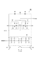
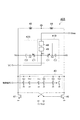
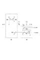
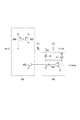
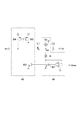
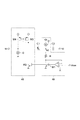
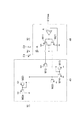
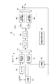
図2は、電圧制御発振器40の回路例を示す図である。この図に示される電圧制御発振器40はLC-VCOである。電圧制御発振器40は、第1容量回路41、第2容量回路42、第3容量回路43、インダクタ44、インダクタ45、NMOSトランジスタ46およびNMOSトランジスタ47を含む。
FIG. 2 is a diagram illustrating a circuit example of the voltage controlled
第1容量回路41および第2容量回路42は共通の構成を有する。第1容量回路41および第2容量回路42それぞれは、可変容量素子C1、容量素子C2および抵抗器Rを含む。可変容量素子C1は、ノードN1とノードN2との間に設けられている。可変容量素子C1の容量値は、ノードN1とノードN2との間の電圧値に依存する。容量素子C2は、ノードN2とノードN3との間に設けられている。容量素子C2の容量値は、ノードN2とノードN3との間の電圧値に依らず一定であってよい。抵抗器Rの一端はノードN2に接続され、抵抗器Rの他端に任意のバイアス電圧値Vbiasが入力される。抵抗器Rの抵抗値は高く、第1容量回路41および第2容量回路42それぞれのノードN2に任意のバイアス電圧値Vbiasが与えられる。
The
第3容量回路43は、第1容量回路41および第2容量回路42それぞれのノードN3に接続されている。第3容量回路43は、第1容量回路41のノードN3に接続された複数の容量素子と、これら複数の容量素子それぞれに対応して直列に接続されたスイッチとを含む。また、第3容量回路43は、第2容量回路42のノードN3に接続された複数の容量素子と、これら複数の容量素子それぞれに対応して直列に接続されたスイッチとを含む。第3容量回路43は、外部から与えられる制御信号により各スイッチのオン/オフの状態が設定されて、これらの設定に応じた容量値を有する。
The
インダクタ44およびインダクタ45は共通の特性を有する。インダクタ44は、電源電位供給端と第1容量回路41のノードN3との間に設けられている。インダクタ45は、電源電位供給端と第2容量回路42のノードN3との間に設けられている。
The
NMOSトランジスタ46およびNMOSトランジスタ47は共通の特性を有する。NMOSトランジスタ46のドレインは第1容量回路41のノードN3に接続されている。NMOSトランジスタ46のソースは接地電位供給端に接続されている。NMOSトランジスタ46のゲートはNMOSトランジスタ47のドレインに接続されている。NMOSトランジスタ47のドレインは第2容量回路42のノードN3に接続されている。NMOSトランジスタ47のソースは接地電位供給端に接続されている。NMOSトランジスタ47のゲートはNMOSトランジスタ46のドレインに接続されている。
The
第1容量回路41および第2容量回路42それぞれのノードN1は共通であり、このノードN1に制御電圧値VCが入力される。第1容量回路41および第2容量回路42それぞれのノードN3(または、これに電気的に接続されたノード)から発振信号CLKoutが出力される。
The node N1 of the
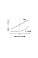
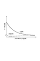
図3は、電圧制御発振器40の特性を説明する図である。この図において、横軸は、電圧制御発振器40に入力される制御電圧値VCである。縦軸は、電圧制御発振器40から出力される発振信号CLKoutの周波数である。この図では、制御電圧値VCと発振信号CLKoutの周波数との間の関係(FV特性)を示す線が9本示されている。制御信号により第3容量回路43の容量値を設定することで、その9つのFV特性のうちの何れか1つのFV特性を選択することができる。そして、その選択したFV特性において制御電圧値VCに対応する周波数の発振信号CLKoutが電圧制御発振器40から出力される。なお、複数のFV特性のうちから一つを選択する必要がなく、FV特性が固定でも構わなければ、第3容量回路43は設けられなくてもよい。
FIG. 3 is a diagram illustrating characteristics of the voltage controlled
ところで、電圧制御発振器40の第1容量回路41および第2容量回路42それぞれに含まれる可変容量素子C1は、ノードN1とノードN2との間に印加される電圧値に応じた量のリーク電流が生じる。そのリーク電流の量によっては、PLL回路1の性能が悪化する。
By the way, the variable capacitance element C1 included in each of the
例えば、可変容量素子は、CMOS微細プロセスによりPウェルに2つのN+領域を有するMOSトランジスタにより構成される。このMOSトランジスタのソースおよびドレインを互いに電気的に接続して一方の端子とし、ゲートを他方の端子としたとき、このMOSトランジスタの接合容量値は、これら2つの端子の間に印加される電圧値に応じたものになる。また、これら2つの端子の間に、印加電圧値に応じた量のリーク電流が生じる。このMOSトランジスタにおけるリーク電流はゲートリークと呼ばれる。近年、プロセスが微細化してゲート酸化膜が薄くなることによりゲートリークは顕在化してきた。 For example, the variable capacitance element is constituted by a MOS transistor having two N + regions in a P well by a CMOS fine process. When the source and the drain of the MOS transistor are electrically connected to each other to form one terminal and the gate to the other terminal, the junction capacitance value of the MOS transistor is a voltage value applied between these two terminals. It depends on. Also, an amount of leak current corresponding to the applied voltage value is generated between these two terminals. The leak current in this MOS transistor is called gate leak. In recent years, gate leakage has become apparent as the process becomes finer and the gate oxide film becomes thinner.
図4は、可変容量素子の特性を説明する図である。この図は、2端子間の印加電圧値と容量値との間の関係、および、2端子間の印加電圧値とリーク電流量との間の関係を示す。この図に示されるように、印加電圧値が0を超えて大きくなると、リーク電流量は急激に大きくなっていく。なお、リーク電流量は、温度によっても大きく変化する。通常は、温度が高いほど、リーク電流量は大きい。リーク電流量は例えば数nA〜数十μAである。 FIG. 4 is a diagram illustrating characteristics of the variable capacitance element. This figure shows the relationship between the applied voltage value between the two terminals and the capacitance value, and the relationship between the applied voltage value between the two terminals and the amount of leakage current. As shown in this figure, when the applied voltage value exceeds 0 and increases, the amount of leak current increases sharply. It should be noted that the amount of leak current varies greatly depending on the temperature. Normally, the higher the temperature, the larger the amount of leakage current. The amount of leakage current is, for example, several nA to several tens μA.
電圧制御発振器40の第1容量回路41および第2容量回路42それぞれに含まれる可変容量素子C1にリーク電流が生じると、その電流は、バイアス電圧値Vbiasの入力端から抵抗器Rおよび可変容量素子C1を経て制御電圧値VCの入力端へ向かう方向に、または、これとは逆の方向に、流れる。電流が流れる方向は、可変容量素子C1の向き及びバイアス電圧値Vbiasに依って異なる。
When a leak current occurs in the variable capacitance element C1 included in each of the
この電流が流れる方向が何れであっても、この電流により、ループフィルタ30の容量素子32,33の蓄積電荷量が変動して、ループフィルタ30から出力される制御電圧値VCが変動する。電圧制御発振器40に入力される制御電圧値VCが変動すると、電圧制御発振器40から出力される発振信号CLKoutの周波数も変動し、位相比較器10に入力される帰還発振信号の周波数も変動する。
Regardless of the direction in which this current flows, the amount of charge stored in the
位相比較器10において、入力信号と帰還発振信号との間の位相差が検出される。この位相差が小さくなるように、チャージポンプ20からループフィルタ30へ充放電電流が入力される。この充放電電流は例えば10μA程度以上である。制御電圧値VCが元の値に戻ることで、電圧制御発振器40から出力される発振信号CLKoutの周波数も元に戻る。
In the
しかし、PLL回路1におけるフィードバックは入力信号の周期毎に行われるので、入力信号の周期(または1ビット当たりの時間)が長いと、1周期の間の発振信号CLKoutの周波数の変動幅が大きくなり、発振信号CLKoutのジッタが大きくなる。また、チャージポンプ20からループフィルタ30へ与えられる充放電電流量より可変容量素子C1のリーク電流量が大きいと、フィードバックによって制御電圧値VCを元の値に戻すことができなくなり、PLL回路として動作しなくなる。
However, since feedback in the
可変容量素子として、例えば以下の二つの素子がある。その一つは、ゲート酸化膜が薄く低電圧(1.0V)で動作して、容量変化量が大きく、リーク電流量が比較的大きい。他の一つは、ゲート酸化膜が厚く高電圧(3.3V)で動作して、容量変化量が小さく、リーク電流量が比較的小さい。後者の高電圧動作の可変容量素子を用いる場合には、容量可変範囲を増やすために制御電圧の範囲を増加させる方法があるが、チャージポンプおよびループフィルタ等の周辺回路をも高電圧で動作するものを用いる必要があり、半導体基板上に集積化する場合にレイアウト面積が大きくなる。また、制御電圧の範囲を増加させずに、可変容量素子のサイズを大きくすることも対策として考えられるが、この場合にもレイアウト面積が大きくなる。 As the variable capacitance element, for example, there are the following two elements. One is that the gate oxide film is thin and operates at a low voltage (1.0 V), the capacitance change is large, and the leak current is relatively large. The other is that the gate oxide film is thick and operates at a high voltage (3.3 V), the capacitance variation is small, and the leakage current is relatively small. In the case of using the latter high-voltage operation variable capacitance element, there is a method of increasing the control voltage range in order to increase the capacitance variable range. However, peripheral circuits such as a charge pump and a loop filter also operate at a high voltage. It is necessary to use a semiconductor device, and the layout area becomes large when integrated on a semiconductor substrate. As a countermeasure, it is possible to increase the size of the variable capacitance element without increasing the range of the control voltage. However, in this case, the layout area also increases.
特許文献1に開示された発明は、LC-VCOの可変容量素子と同等の可変容量素子を含むレプリカ回路を設け、このレプリカ回路の可変容量素子のリーク電流によりLC-VCOの可変容量素子のリーク電流を補償することにより、LC-VCOの性能悪化を抑制することを図る。しかし、この場合もレイアウト面積が大きくなる。また、LC-VCOの可変容量素子とレプリカ回路の可変容量素子との間で特性が相違していると、各々の可変容量素子に流れるリーク電流が相違し、十分に補償をすることができない。それ故、LC-VCOの性能悪化を十分に抑制することができず、また、これを用いるPLL回路またはCDR装置の性能悪化を十分に抑制することもできない。
In the invention disclosed in
以下に説明する実施形態は、このような問題点を解消し得るものである。
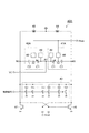
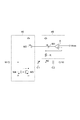
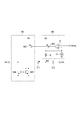
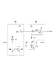
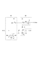
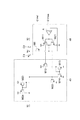
図5は、電圧制御発振器40Aの構成を示す図である。この図に示される電圧制御発振器40Aは、第1容量回路41A、第2容量回路42A、第3容量回路43、インダクタ44、インダクタ45、NMOSトランジスタ46およびNMOSトランジスタ47を備える。図2に示された電圧制御発振器40の構成と比較すると、図5に示される電圧制御発振器40Aは、第1容量回路41に替えて第1容量回路41Aを備える点で相違し、第2容量回路42に替えて第2容量回路42Aを備える点で相違する。
The embodiment described below can solve such a problem.
FIG. 5 is a diagram showing a configuration of the voltage controlled
第1容量回路41Aおよび第2容量回路42Aは共通の構成を有する。第1容量回路41Aおよび第2容量回路42Aそれぞれは、可変容量素子C1、容量素子C2、検出回路48および補償回路49を含む。可変容量素子C1は、ノードN1とノードN2との間に設けられている。可変容量素子C1の容量値は、ノードN1とノードN2との間の電圧値に依存する。容量素子C2は、ノードN2とノードN3との間に設けられている。容量素子C2の容量値は、ノードN2とノードN3との間の電圧値に依らず一定であってよい。検出回路48は、ノードN2にバイアス電圧値Vbiasを与えるとともに、可変容量素子C1に流れるリーク電流の量を検出する。補償回路49は、検出回路48による検出結果に基づいて、可変容量素子C1のリーク電流を補償する電流をノードN1に流す。
The
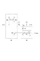
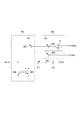
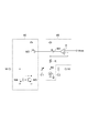
図6は、電圧制御発振器40Bの構成を示す図である。この図に示される電圧制御発振器40Bは、第1容量回路41B、第2容量回路42B、第3容量回路43、インダクタ44、インダクタ45、NMOSトランジスタ46およびNMOSトランジスタ47を備える。図5に示された電圧制御発振器40Aの構成と比較すると、図6に示される電圧制御発振器40Bは、第1容量回路41Aに替えて第1容量回路41Bを備える点で相違し、第2容量回路42Aに替えて第2容量回路42Bを備える点で相違する。
FIG. 6 is a diagram showing a configuration of the voltage controlled
第1容量回路41Bおよび第2容量回路42Bは共通の構成を有する。第1容量回路41Bおよび第2容量回路42Bそれぞれは、可変容量素子C1、容量素子C2、検出回路48および補償回路49を含む。本構成では、第1容量回路41Bおよび第2容量回路42Bそれぞれの検出回路48が共通である。また、第1容量回路41Bおよび第2容量回路42Bそれぞれの補償回路49が共通である。
The
なお、電圧制御発振器40A(図5)および電圧制御発振器40B(図6)それぞれにおいて、複数のFV特性のうちから一つを選択する必要がなく、FV特性が固定でも構わなければ、第3容量回路43は設けられなくてもよい。
In each of the voltage controlled
図7は、検出回路48および補償回路49の第1回路例を示す図である。第1回路例では、検出回路48は、PMOSトランジスタM1、抵抗器Rおよび差動アンプAを含む。補償回路49は、PMOSトランジスタM2、NMOSトランジスタM3およびNMOSトランジスタM4を含む。
FIG. 7 is a diagram illustrating a first circuit example of the
検出回路48において、PMOSトランジスタM1のソースは、電源電位供給端に接続されている。抵抗器Rは、PMOSトランジスタM1のドレインとノードN2との間に設けられている。差動アンプAの非反転入力端子は、PMOSトランジスタM1のドレインに接続されている。差動アンプAの反転入力端子は、バイアス電圧値Vbiasが入力される。差動アンプAの出力端子は、PMOSトランジスタM1のゲートに接続されている。
In the
補償回路49において、PMOSトランジスタM2のソースは、電源電位供給端に接続されている。PMOSトランジスタM2のゲートは、差動アンプAの出力端子に接続されている。NMOSトランジスタM3のソースは、接地電位供給端に接続されている。NMOSトランジスタM3のドレインは、PMOSトランジスタM2のドレインに接続されている。NMOSトランジスタM4のソースは、接地電位供給端に接続されている。NMOSトランジスタM4のドレインは、ノードN1に接続されている。NMOSトランジスタM4のゲートは、NMOSトランジスタM3のゲートおよびドレインに接続されている。NMOSトランジスタM4は、NMOSトランジスタM3とともにカレントミラー回路を構成し、NMOSトランジスタM3に流れる電流と同じ量の電流を流す。
In the
検出回路48において、差動アンプAの反転入力端子と非反転入力端子とはイマジナリショートの関係を有することから、差動アンプAの反転入力端子は非反転入力端子と同じバイアス電圧値Vbiasとされ、そのバイアス電圧値Vbiasが抵抗器Rを介してノードN2に与えられる。可変容量素子C1のリーク電流は、電源電位供給端からPMOSトランジスタM1,抵抗器Rおよび可変容量素子C1を経てノードN1へ流れる。すなわち、PMOSトランジスタM1に流れる電流の量は、可変容量素子C1のリーク電流量と同じである。差動アンプAの出力端子からPMOSトランジスタM1のゲートに与えられる電圧値は、可変容量素子C1のリーク電流量と同じ量の電流がPMOSトランジスタM1に流れるような値となる。
In the
補償回路49において、差動アンプAの出力端子からPMOSトランジスタM2のゲートに与えられる電圧値は、差動アンプAの出力端子からPMOSトランジスタM1のゲートに与えられる電圧値と同じである。したがって、PMOSトランジスタM2に流れる電流の量は、PMOSトランジスタM1に流れる電流の量と同じである。PMOSトランジスタM2に流れる電流は、NMOSトランジスタM3にも流れる。NMOSトランジスタM4とNMOSトランジスタM3とはカレントミラー回路を構成しているから、NMOSトランジスタM4に流れる電流の量は、PMOSトランジスタM3に流れる電流の量と同じである。すなわち、NMOSトランジスタM4に流れる電流の量は、可変容量素子C1のリーク電流量と同じである。したがって、NMOSトランジスタM4に流れる電流は、可変容量素子C1のリーク電流を補償することができる。
In the
図8は、検出回路48および補償回路49の第2回路例を示す図である。第2回路例では、検出回路48は、NMOSトランジスタM1、抵抗器Rおよび差動アンプAを含む。また、補償回路49は、NMOSトランジスタM2、PMOSトランジスタM3およびPMOSトランジスタM4を含む。
FIG. 8 is a diagram showing a second circuit example of the
検出回路48において、NMOSトランジスタM1のソースは、接地電位供給端に接続されている。抵抗器Rは、NMOSトランジスタM1のドレインとノードN2との間に設けられている。差動アンプAの非反転入力端子は、NMOSトランジスタM1のドレインに接続されている。差動アンプAの反転入力端子は、バイアス電圧値Vbiasが入力される。差動アンプAの出力端子は、NMOSトランジスタM1のゲートに接続されている。
In the
補償回路49において、NMOSトランジスタM2のソースは、接地電位供給端に接続されている。NMOSトランジスタM2のゲートは、差動アンプAの出力端子に接続されている。PMOSトランジスタM3のソースは、電源電位供給端に接続されている。PMOSトランジスタM3のドレインは、NMOSトランジスタM2のドレインに接続されている。PMOSトランジスタM4のソースは、電源電位供給端に接続されている。PMOSトランジスタM4のドレインは、ノードN1に接続されている。PMOSトランジスタM4のゲートは、PMOSトランジスタM3のゲートおよびドレインに接続されている。PMOSトランジスタM4は、PMOSトランジスタM3とともにカレントミラー回路を構成し、PMOSトランジスタM3に流れる電流と同じ量の電流を流す。
In the
検出回路48において、差動アンプAの反転入力端子と非反転入力端子とはイマジナリショートの関係を有することから、差動アンプAの反転入力端子は非反転入力端子と同じバイアス電圧値Vbiasとされ、そのバイアス電圧値Vbiasが抵抗器Rを介してノードN2に与えられる。可変容量素子C1のリーク電流は、ノードN1から可変容量素子C1,抵抗器RおよびNMOSトランジスタM1を経て接地電位供給端へ流れる。すなわち、NMOSトランジスタM1に流れる電流の量は、可変容量素子C1のリーク電流量と同じである。差動アンプAの出力端子からNMOSトランジスタM1のゲートに与えられる電圧値は、可変容量素子C1のリーク電流量と同じ量の電流がNMOSトランジスタM1に流れるような値となる。
In the
補償回路49において、差動アンプAの出力端子からNMOSトランジスタM2のゲートに与えられる電圧値は、差動アンプAの出力端子からNMOSトランジスタM1のゲートに与えられる電圧値と同じである。したがって、NMOSトランジスタM2に流れる電流の量は、NMOSトランジスタM1に流れる電流の量と同じである。NMOSトランジスタM2に流れる電流は、PMOSトランジスタM3にも流れる。PMOSトランジスタM4とPMOSトランジスタM3とはカレントミラー回路を構成しているから、PMOSトランジスタM4に流れる電流の量は、NMOSトランジスタM3に流れる電流の量と同じである。すなわち、PMOSトランジスタM4に流れる電流の量は、可変容量素子C1のリーク電流量と同じである。したがって、PMOSトランジスタM4に流れる電流は、可変容量素子C1のリーク電流を補償することができる。
In the
図9は、検出回路48および補償回路49の第3回路例を示す図である。第3回路例では、検出回路48は、PMOSトランジスタM1、PMOSトランジスタM5および差動アンプAを含む。また、補償回路49は、PMOSトランジスタM2、NMOSトランジスタM3およびNMOSトランジスタM4を含む。
FIG. 9 is a diagram illustrating a third circuit example of the
第1回路例(図7)と比較すると、第3回路例(図9)は、検出回路48が抵抗器Rに替えてPMOSトランジスタM5を含む点で相違する。PMOSトランジスタM5は、PMOSトランジスタM1のドレインとノードN2との間に設けられている。PMOSトランジスタM5は、抵抗器Rと同様に抵抗部として用いられるものであり、ゲートに与えられる参照電圧値Vrefに応じた抵抗値を有する。PMOSトランジスタM5を抵抗部として用いることで、小さいレイアウト面積で高抵抗の抵抗部を実現することができる。
As compared with the first circuit example (FIG. 7), the third circuit example (FIG. 9) is different in that the
図10は、検出回路48および補償回路49の第4回路例を示す図である。第4回路例では、検出回路48は、NMOSトランジスタM1、NMOSトランジスタM5および差動アンプAを含む。また、補償回路49は、NMOSトランジスタM2、PMOSトランジスタM3およびPMOSトランジスタM4を含む。
FIG. 10 is a diagram illustrating a fourth circuit example of the
第2回路例(図8)と比較すると、第4回路例(図10)は、検出回路48が抵抗器Rに替えてNMOSトランジスタM5を含む点で相違する。NMOSトランジスタM5は、NMOSトランジスタM1のドレインとノードN2との間に設けられている。NMOSトランジスタM5は、抵抗器Rと同様に抵抗部として用いられるものであり、ゲートに与えられる参照電圧値Vrefに応じた抵抗値を有する。NMOSトランジスタM5を抵抗部として用いることで、小さいレイアウト面積で高抵抗の抵抗部を実現することができる。
Compared to the second circuit example (FIG. 8), the fourth circuit example (FIG. 10) is different in that the
これまでに説明した第1回路例(図7)、第2回路例(図8)、第3回路例(図9)および第4回路例(図10)では、制御電圧値VCの大きさによっては、リーク電流が小さくなって、検出回路48によるリーク電流量の検出ができず、補償回路49によるリーク電流の補償ができない可能性がある。その対策として、以下に説明する第5回路例(図11)、第6回路例(図12)、第7回路例(図13)および第8回路例(図14)のように、ダミーのリーク電流を流す第1電流源I1または第2電流源I2を設けるのが好適である。第1電流源I1または第2電流源I2が流すダミーのリーク電流の量は数十nA程度であるのが妥当である。このようなダミーのリーク電流を流すことは、回路起因のリーク電流になる。しかし、ダミーのリーク電流の量は、チャージポンプからの電流の量と比べて1/100程度であって十分に小さいことから、誤差として扱うことができる。
In the first circuit example (FIG. 7), the second circuit example (FIG. 8), the third circuit example (FIG. 9), and the fourth circuit example (FIG. 10) described above, depending on the magnitude of the control voltage value VC. In this case, there is a possibility that the leakage current becomes small, the
図11は、検出回路48および補償回路49の第5回路例を示す図である。第5回路例では、検出回路48は、PMOSトランジスタM1、抵抗器R、差動アンプAおよび第1電流源I1を含む。また、補償回路49は、PMOSトランジスタM2、NMOSトランジスタM3およびNMOSトランジスタM4を含む。第1回路例(図7)と比較すると、第5回路例(図11)は、検出回路48が第1電流源I1を更に含む点で相違する。第1電流源I1は、接地電位供給端とPMOSトランジスタM1のドレインとの間に設けられている。
FIG. 11 is a diagram illustrating a fifth circuit example of the
図12は、検出回路48および補償回路49の第6回路例を示す図である。第6回路例では、検出回路48は、NMOSトランジスタM1、抵抗器R、差動アンプAおよび第1電流源I1を含む。また、補償回路49は、NMOSトランジスタM2、PMOSトランジスタM3およびPMOSトランジスタM4を含む。第2回路例(図8)と比較すると、第6回路例(図12)は、検出回路48が第1電流源I1を更に含む点で相違する。第1電流源I1は、電源電位供給端とNMOSトランジスタM1のドレインとの間に設けられている。
FIG. 12 is a diagram illustrating a sixth circuit example of the
図13は、検出回路48および補償回路49の第7回路例を示す図である。第7回路例では、検出回路48は、PMOSトランジスタM1、抵抗器R、差動アンプAおよび第2電流源I2を含む。また、補償回路49は、PMOSトランジスタM2、NMOSトランジスタM3およびNMOSトランジスタM4を含む。第1回路例(図7)と比較すると、第7回路例(図11)は、検出回路48が第2電流源I2を更に含む点で相違する。第2電流源I2は、接地電位供給端とノードN2との間に設けられている。
FIG. 13 is a diagram illustrating a seventh circuit example of the
図14は、検出回路48および補償回路49の第8回路例を示す図である。第8回路例では、検出回路48は、NMOSトランジスタM1、抵抗器R、差動アンプAおよび第2電流源I2を含む。また、補償回路49は、NMOSトランジスタM2、PMOSトランジスタM3およびPMOSトランジスタM4を含む。第2回路例(図8)と比較すると、第8回路例(図12)は、検出回路48が第2電流源I2を更に含む点で相違する。第2電流源I2は、電源電位供給端とノードN2との間に設けられている。
FIG. 14 is a diagram illustrating an eighth circuit example of the
第5回路例(図11)、第6回路例(図12)、第7回路例(図13)および第8回路例(図14)それぞれにおいて、第3回路例(図9)および第4回路例(図10)と同様に、抵抗器Rに替えてMOSトランジスタM5を設けてもよい。 In the fifth circuit example (FIG. 11), the sixth circuit example (FIG. 12), the seventh circuit example (FIG. 13) and the eighth circuit example (FIG. 14), respectively, the third circuit example (FIG. 9) and the fourth circuit example As in the example (FIG. 10), a MOS transistor M5 may be provided instead of the resistor R.
これまでに説明した第5回路例(図11)、第6回路例(図12)、第7回路例(図13)および第8回路例(図14)では、第1電流源I1または第2電流源I2が流すダミーのリーク電流により誤差が生じる。以下に説明する第9回路例(図15)、第10回路例(図16)、第11回路例(図17)および第12回路例(図18)では、この誤差を抑制するための第3電流源I3または第4電流源I4を設ける。 In the fifth circuit example (FIG. 11), the sixth circuit example (FIG. 12), the seventh circuit example (FIG. 13), and the eighth circuit example (FIG. 14) described above, the first current source I1 or the second current example An error occurs due to a dummy leak current flowing from the current source I2. In the ninth circuit example (FIG. 15), the tenth circuit example (FIG. 16), the eleventh circuit example (FIG. 17), and the twelfth circuit example (FIG. 18) described below, a third circuit example for suppressing this error is used. A current source I3 or a fourth current source I4 is provided.
図15は、検出回路48および補償回路49の第9回路例を示す図である。第9回路例では、検出回路48は、PMOSトランジスタM1、抵抗器R、差動アンプAおよび第2電流源I2を含む。また、補償回路49は、PMOSトランジスタM2、NMOSトランジスタM3、NMOSトランジスタM4および第3電流源I3を含む。第7回路例(図13)と比較すると、第9回路例(図15)は、補償回路49が第3電流源I3を更に含む点で相違する。第3電流源I3は、電源電位供給端とノードN1との間に設けられている。第3電流源I3が流す電流の量は、第2電流源I2が流す電流の量と同じである。
FIG. 15 is a diagram illustrating a ninth circuit example of the
図16は、検出回路48および補償回路49の第10回路例を示す図である。第10回路例では、検出回路48は、NMOSトランジスタM1、抵抗器R、差動アンプAおよび第2電流源I2を含む。また、補償回路49は、NMOSトランジスタM2、PMOSトランジスタM3、PMOSトランジスタM4および第3電流源I3を含む。第8回路例(図14)と比較すると、第10回路例(図16)は、補償回路49が第3電流源I3を更に含む点で相違する。第3電流源I3は、接地電位供給端とノードN1との間に設けられている。第3電流源I3が流す電流の量は、第2電流源I2が流す電流の量と同じである。
FIG. 16 is a diagram illustrating a tenth circuit example of the
図17は、検出回路48および補償回路49の第11回路例を示す図である。第11回路例では、検出回路48は、PMOSトランジスタM1、抵抗器R、差動アンプAおよび第2電流源I2を含む。また、補償回路49は、PMOSトランジスタM2、NMOSトランジスタM3、NMOSトランジスタM4および第4電流源I4を含む。第7回路例(図13)と比較すると、第11回路例(図17)は、補償回路49が第4電流源I4を更に含む点で相違する。第4電流源I4は、接地電位供給端とNMOSトランジスタM3およびNMOSトランジスタM4それぞれのゲートとの間に設けられている。第4電流源I4が流す電流の量は、第2電流源I2が流す電流の量と同じである。
FIG. 17 is a diagram illustrating an eleventh circuit example of the
図18は、検出回路48および補償回路49の第12回路例を示す図である。第12回路例では、検出回路48は、NMOSトランジスタM1、抵抗器R、差動アンプAおよび第2電流源I2を含む。また、補償回路49は、NMOSトランジスタM2、PMOSトランジスタM3、PMOSトランジスタM4および第4電流源I4を含む。第8回路例(図14)と比較すると、第12回路例(図18)は、補償回路49が第4電流源I4を更に含む点で相違する。第4電流源I4は、電源電位供給端とPMOSトランジスタM3およびPMOSトランジスタM4それぞれのゲートとの間に設けられている。第4電流源I4が流す電流の量は、第2電流源I2が流す電流の量と同じである。
FIG. 18 is a diagram illustrating a twelfth circuit example of the
第9回路例(図15)、第10回路例(図16)、第11回路例(図17)および第12回路例(図18)それぞれにおいて、第3回路例(図9)および第4回路例(図10)と同様に、抵抗器Rに替えてMOSトランジスタM5を設けてもよい。また、第5回路例(図11)および第6回路例(図12)それぞれに対して、第3電流源I3または第4電流源I4を設けてもよい。 In the ninth circuit example (FIG. 15), the tenth circuit example (FIG. 16), the eleventh circuit example (FIG. 17), and the twelfth circuit example (FIG. 18), respectively, the third circuit example (FIG. 9) and the fourth circuit example As in the example (FIG. 10), a MOS transistor M5 may be provided instead of the resistor R. Further, a third current source I3 or a fourth current source I4 may be provided for each of the fifth circuit example (FIG. 11) and the sixth circuit example (FIG. 12).
これまでに説明した第5〜第12の各回路例は、第1電流源I1または第2電流源I2によりダミーのリーク電流を流すものであった。また、第9〜第12の各回路例は、第1電流源I1または第2電流源I2が流すダミーのリーク電流により生じる誤差を第3電流源I3または第4電流源I4により抑制するものであった。以下に説明する第13回路例(図19)、第14回路例(図20)および第15回路例(図21)は、電流源を付加することなく、検出回路48および補償回路49を構成することができる。
In each of the fifth to twelfth circuit examples described above, a dummy leak current is caused to flow by the first current source I1 or the second current source I2. The ninth to twelfth circuit examples suppress errors caused by a dummy leak current flowing from the first current source I1 or the second current source I2 by the third current source I3 or the fourth current source I4. there were. The thirteenth circuit example (FIG. 19), the fourteenth circuit example (FIG. 20), and the fifteenth circuit example (FIG. 21) described below constitute the
図19は、検出回路48および補償回路49の第13回路例を示す図である。第13回路例では、検出回路48は、PMOSトランジスタM11、NMOSトランジスタM21、抵抗器Rおよび差動アンプAを含む。補償回路49は、PMOSトランジスタM12、NMOSトランジスタM13、NMOSトランジスタM14、NMOSトランジスタM22、PMOSトランジスタM23およびPMOSトランジスタM24を含む。
FIG. 19 is a diagram illustrating a thirteenth circuit example of the
検出回路48において、PMOSトランジスタM11のソースは、電源電位供給端に接続されている。NMOSトランジスタM21のソースは、接地電位供給端に接続されている。PMOSトランジスタM11およびNMOSトランジスタM21それぞれのドレインは、互いに接続されている。抵抗器Rは、PMOSトランジスタM11およびNMOSトランジスタM21それぞれのドレインとノードN2との間に設けられている。差動アンプAの非反転入力端子は、PMOSトランジスタM11およびNMOSトランジスタM21それぞれのドレインに接続されている。差動アンプAの反転入力端子は、バイアス電圧値Vbiasが入力される。差動アンプAの出力端子は、PMOSトランジスタM11およびNMOSトランジスタM21それぞれのゲートに接続されている。
In the
補償回路49において、PMOSトランジスタM12のソースは、電源電位供給端に接続されている。PMOSトランジスタM12のゲートは、差動アンプAの出力端子に接続されている。NMOSトランジスタM13のソースは、接地電位供給端に接続されている。NMOSトランジスタM13のドレインは、PMOSトランジスタM12のドレインに接続されている。NMOSトランジスタM14のソースは、接地電位供給端に接続されている。NMOSトランジスタM14のドレインは、ノードN1に接続されている。NMOSトランジスタM14のゲートは、NMOSトランジスタM13のゲートおよびドレインに接続されている。NMOSトランジスタM14は、NMOSトランジスタM13とともにカレントミラー回路を構成し、NMOSトランジスタM13に流れる電流と同じ量の電流を流す。
In the
また、補償回路49において、NMOSトランジスタM22のソースは、接地電位供給端に接続されている。NMOSトランジスタM22のゲートは、差動アンプAの出力端子に接続されている。PMOSトランジスタM23のソースは、電源電位供給端に接続されている。PMOSトランジスタM23のドレインは、NMOSトランジスタM22のドレインに接続されている。PMOSトランジスタM24のソースは、電源電位供給端に接続されている。PMOSトランジスタM24のドレインは、ノードN1に接続されている。PMOSトランジスタM24のゲートは、PMOSトランジスタM23のゲートおよびドレインに接続されている。PMOSトランジスタM24は、PMOSトランジスタM23とともにカレントミラー回路を構成し、PMOSトランジスタM23に流れる電流と同じ量の電流を流す。
In the
検出回路48および補償回路49の第13回路例(図19)は、第1回路例(図7)および第2回路例(図8)の双方の構成を含む構成とした上で、第1回路例(図7)および第2回路例(図8)それぞれに含まれる抵抗器Rおよび差動アンプAを共通化したものである。検出回路48におけるPMOSトランジスタM11およびNMOSトランジスタM21は、プッシュ・プル・バッファを構成している。
The thirteenth circuit example (FIG. 19) of the
図20は、検出回路48および補償回路49の第14回路例を示す図である。図21は、検出回路48および補償回路49の第15回路例を示す図である。第14回路例(図20)および第15回路例(図21)それぞれでは、検出回路48は、PMOSトランジスタM11、NMOSトランジスタM21、MOSトランジスタM5および差動アンプAを含む。補償回路49は、PMOSトランジスタM12、NMOSトランジスタM13、NMOSトランジスタM14、NMOSトランジスタM22、PMOSトランジスタM23およびPMOSトランジスタM24を含む。
FIG. 20 is a diagram illustrating a fourteenth circuit example of the
第13回路例(図19)と比較すると、第14回路例(図20)および第15回路例(図21)それぞれは、検出回路48が抵抗器Rに替えてMOSトランジスタM5を含む点で相違する。MOSトランジスタM5は、PMOSトランジスタM11およびNMOSトランジスタM21それぞれのドレインとノードN2との間に設けられている。MOSトランジスタM5は、抵抗器Rと同様に抵抗部として用いられるものであり、ゲートに与えられる参照電圧値Vrefに応じた抵抗値を有する。MOSトランジスタM5を抵抗部として用いることで、小さいレイアウト面積で高抵抗の抵抗部を実現することができる。
Compared with the thirteenth circuit example (FIG. 19), the fourteenth circuit example (FIG. 20) and the fifteenth circuit example (FIG. 21) are different in that the
第14回路例(図20)と第15回路例(図21)とは、可変容量素子C1に流れるリーク電流の向きの点で相違する。第14回路例(図20)では、可変容量素子C1のリーク電流は、ノードN1から可変容量素子C1,MOSトランジスタM5およびNMOSトランジスタM21を経て接地電位供給端へ流れる。第15回路例(図21)では、可変容量素子C1のリーク電流は、電源電位供給端からPMOSトランジスタM11,MOSトランジスタM5および可変容量素子C1を経てノードN1へ流れる。 The fourteenth circuit example (FIG. 20) and the fifteenth circuit example (FIG. 21) differ in the direction of the leak current flowing through the variable capacitance element C1. In the fourteenth circuit example (FIG. 20), the leak current of the variable capacitance element C1 flows from the node N1 to the ground potential supply terminal via the variable capacitance element C1, the MOS transistor M5, and the NMOS transistor M21. In the fifteenth circuit example (FIG. 21), the leak current of the variable capacitance element C1 flows from the power supply potential supply terminal to the node N1 via the PMOS transistor M11, the MOS transistor M5, and the variable capacitance element C1.
図22は、第1回路例(図7)を採用した電圧制御発振器40B(図6)の構成を示す図である。検出回路48は、LDO(Low Dropout)構成を有しており、差動アンプAの反転入力端子に入力されるバイアス電圧値Vbiasと同じ電圧値を、差動アンプAの非反転入力端子から抵抗器Rを介してノードN2に与える。PMOSトランジスタM1には、2個の可変容量素子C1のリーク電流と同量の電流が流れる。PMOSトランジスタM2に流れる電流の量は、PMOSトランジスタM1に流れる電流の量と同じである。PMOSトランジスタM2に流れる電流は、NMOSトランジスタM3にも流れる。NMOSトランジスタM4とNMOSトランジスタM3とはカレントミラー回路を構成しているから、NMOSトランジスタM4に流れる電流の量は、PMOSトランジスタM3に流れる電流の量と同じである。すなわち、NMOSトランジスタM4に流れる電流の量は、2個の可変容量素子C1のリーク電流量と同じである。したがって、NMOSトランジスタM4に流れる電流は、2個の可変容量素子C1のリーク電流を補償することができる。
FIG. 22 is a diagram showing a configuration of a voltage controlled
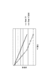
図23は、可変容量素子における2端子間の印加電圧値とリーク電流量との間の関係を示す図である。ここでのリーク電流は、可変容量素子C1のリーク電流のうち電圧制御発振器からチャージポンプへ流れる電流(または、これとは逆の方向に流れる電流)を表す。この図は、検出回路48および補償回路49が設けられていない比較例、および、検出回路48および補償回路49が設けられている実施形態、それぞれについて示す。検出回路48および補償回路49が設けられることにより、可変容量素子C1のリーク電流のうち電圧制御発振器からチャージポンプへ流れる電流の量は大きく減少する。
FIG. 23 is a diagram illustrating a relationship between an applied voltage value between two terminals and a leak current amount in the variable capacitance element. Here, the leak current indicates a current flowing from the voltage controlled oscillator to the charge pump (or a current flowing in the opposite direction) from the leak current of the variable capacitance element C1. This figure shows a comparative example in which the
図24は、PLL回路における制御電圧値VCおよび発振信号CLKoutの周波数それぞれの時間変化を示す図である。この図も、検出回路48および補償回路49が設けられていない比較例、および、検出回路48および補償回路49が設けられている実施形態、それぞれについて示す。検出回路48および補償回路49が設けられることにより、制御電圧値VCの変動幅は小さく、また、発振信号CLKoutの周波数の変動幅も小さい。
FIG. 24 is a diagram showing a time change of each of the control voltage value VC and the frequency of the oscillation signal CLKout in the PLL circuit. This figure also shows a comparative example in which the
本実施形態では、レプリカの可変容量素子が不要であるので、LC-VCOの可変容量素子とレプリカの可変容量素子との間の特性の相違の問題が生じることはない。本実施形態では、可変容量素子のリーク電流による性能悪化を抑制することができ、レイアウト面積の増加を抑制することができる。 In the present embodiment, since the variable capacitance element of the replica is unnecessary, the problem of the difference in characteristics between the variable capacitance element of the LC-VCO and the variable capacitance element of the replica does not occur. In the present embodiment, it is possible to suppress the performance deterioration due to the leak current of the variable capacitance element, and to suppress the increase in the layout area.
次に、PLL回路の実施形態について説明する。本実施形態のPLL回路は、PLL回路1(図1)において電圧制御発振器40として電圧制御発振器40A(図5)または電圧制御発振器40B(図6)を採用したものである。また、電圧制御発振器40A(図5)または電圧制御発振器40B(図6)において、検出回路48および補償回路49として第1〜第15の回路例の何れか(または、これらの組合せ若しくは変形例)を採用することができる。本実施形態のPLL回路は、図25に示される構成を有するのが好ましい。
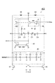
Next, an embodiment of the PLL circuit will be described. The PLL circuit of the present embodiment employs the voltage controlled
図25は、PLL回路1Aの構成を示す図である。PLL回路1Aは、位相比較器10、チャージポンプ20、ループフィルタ30、電圧制御発振器401,402、分周器50および選択部60を備える。図1に示されたPLL回路1の構成と比較すると、図25に示されるPLL回路1Aは、1個の電圧制御発振器40に替えて複数個の電圧制御発振器(図では2個の電圧制御発振器401,402)を備える点で相違し、また、選択部60を更に備える点で相違する。電圧制御発振器401,402それぞれは、電圧制御発振器40A(図5)または電圧制御発振器40B(図6)と同様の構成を有する。
FIG. 25 is a diagram showing a configuration of the
電圧制御発振器401,402それぞれは、制御電圧値VCと発振信号CLKoutの周波数との間の関係(FV特性)が相違している。選択部60は、電圧制御発振器401,402のうち何れか1つの電圧制御発振器から出力される発振信号を選択して分周器50へ出力する。これにより、1個の電圧制御発振器が設けられる場合と比較して、このPLL回路1Aでは動作可能な周波数範囲を拡大することができる。
Each of the voltage controlled
また、電圧制御発振器401,402それぞれに入力される制御電圧値VCは共通である。これにより、チャージポンプ20およびループフィルタ30それぞれを1個だけ設ければよいので、回路規模の増大を抑制することができる。
The control voltage value VC input to each of the voltage controlled
電圧制御発振器401,402のうち何れか1個が使用状態となり、その他は不使用状態となる。ループフィルタ30の容量素子33の容量値には、電圧制御発振器401,402それぞれの可変容量素子C1の容量値が付加される。不使用状態の電圧制御発振器において、ノードN2に与えられるバイアス電圧値Vbiasが、ノードN1に与えられる制御電圧値VCより小さいと、可変容量素子C1のリーク電流量が小さくなり、ループフィルタ30への影響が小さい。しかし、制御電圧値VCの変動によって可変容量素子C1の容量値が変動し、この可変容量素子C1の容量値の変動が、ループフィルタ30の容量素子33の容量値に影響を与える。
1 one of the voltage controlled
そこで、不使用状態の電圧制御発振器において、ノードN2に与える電圧値を一定のバイアス電圧値Vbiasに替えて制御電圧値VCとすることで、可変容量素子C1の容量値の変動を抑制するのが好適である。すなわち、電圧制御発振器401,402それぞれは、ノードN2に与える電圧値として一定のバイアス電圧値Vbiasおよび制御電圧値VCのうちから何れか一方を選択するスイッチを備えるのが好適である。使用状態の電圧制御発振器は、一定のバイアス電圧値Vbiasをスイッチにより選択してノードN2に与える。不使用状態の電圧制御発振器は、制御電圧値VCをスイッチにより選択してノードN2に与える。これにより、不使用状態の電圧制御発振器において、可変容量素子C1の容量値の変動を抑制することができ、また、可変容量素子C1のリーク電流を抑制することができる。
Therefore, in the voltage-controlled oscillator in the unused state, the voltage value applied to the node N2 is changed to the control voltage value VC instead of the constant bias voltage value Vbias, thereby suppressing the fluctuation of the capacitance value of the variable capacitance element C1. It is suitable. That is, it is preferable that each of the voltage controlled
図26は、電圧制御発振器401,402それぞれの可変容量素子C1の容量値が付加されたループフィルタ30の容量素子33の容量値と制御電圧値VCとの間の関係を示すグラフである。この図は、不使用状態の電圧制御発振器において一定のバイアス電圧値(0V)をノードN2に与えた場合、および、不使用状態の電圧制御発振器において制御電圧値VCをノードN2に与えた場合を示す。後者の場合の方が、ループフィルタ30の容量素子33の容量値の変動が小さい。
FIG. 26 is a graph illustrating the relationship between the control voltage value VC and the capacitance value of the
ループフィルタ30の容量素子33の容量値の変動が小さい方が、設計パラメータのばらつきが少なく、設計が容易になる。このような構成により、使用状態の電圧制御発振器における可変容量素子C1のリーク電流を抑制することができ、また、不使用状態の電圧制御発振器における可変容量素子C1の容量値の変動を抑制することができて、ループフィルタ30の容量素子33の容量値の変動を抑制することができる。また、不使用状態の電圧制御発振器における可変容量素子C1のリーク電流があっても、そのリーク電流を補償することができる。
The smaller the fluctuation of the capacitance value of the
次に、CDR装置の実施形態について説明する。CDR装置は、クロックが埋め込まれたデジタル信号(例えば8B10B又は128B130Bのコーディングデータ)を入力し、このデジタル信号に基づいてデータおよびクロックを復元して、その復元データおよび復元クロックを出力するものである。CDR装置は、PLL回路およびサンプラを備えて構成される。CDR装置において、サンプラは、復元クロックが指示するタイミングでデジタル信号のデータをサンプリングして、そのサンプリングしたデータを復元データとして復元クロックに同期して出力する。PLL回路は、入力信号として復元データを位相比較器に入力し、電圧制御発振器から発振信号として復元クロックを出力するともに、復元クロックをサンプラに与える。本実施形態のCDR装置は、前述した本実施形態のPLL回路を備える。本実施形態のCDR装置は、図27に示される構成を有するのが好ましい。 Next, an embodiment of a CDR device will be described. The CDR device inputs a digital signal (for example, coding data of 8B10B or 128B130B) in which a clock is embedded, restores data and a clock based on the digital signal, and outputs restored data and a restored clock. . The CDR device includes a PLL circuit and a sampler. In the CDR device, the sampler samples digital signal data at a timing indicated by the restored clock, and outputs the sampled data as restored data in synchronization with the restored clock. The PLL circuit inputs restored data as an input signal to the phase comparator, outputs a restored clock as an oscillation signal from the voltage controlled oscillator, and supplies the restored clock to the sampler. The CDR device of the present embodiment includes the PLL circuit of the present embodiment described above. The CDR device of the present embodiment preferably has the configuration shown in FIG.
図27は、CDR装置2の構成を示す図である。CDR装置2は、位相比較器101,102、チャージポンプ20、ループフィルタ30、電圧制御発振器401,402、分周器50,51、選択部60,61、サンプラ70および周波数同期検出部80を備える。これらのうち、位相比較器101、チャージポンプ20、ループフィルタ30、電圧制御発振器401および分周器50を含むループは、第1のPLL回路を構成している。位相比較器102、チャージポンプ20、ループフィルタ30および電圧制御発振器402を含むループは、第2のPLL回路を構成している。これら第1および第2のPLL回路において、チャージポンプ20およびループフィルタ30は共通に設けられている。第2のPLL回路は分周器を含まない。
FIG. 27 is a diagram illustrating a configuration of the
サンプラ70は、クロックが埋め込まれたデジタル信号を入力するとともに、選択部60により選択されて出力された発振信号(復元クロック)を入力する。サンプラ70は、復元クロックが指示するタイミングでデジタル信号のデータをサンプリングして、そのサンプリングしたデータを復元データとして復元クロックに同期して位相比較器102へ出力する。
The
位相比較器102は、サンプラ70から復元データを入力するとともに、選択部60により選択されて出力された発振信号(復元クロック)を入力する。位相比較器102は、これら復元クロックと復元データとの間の位相差を検出して、この位相差を表す位相差信号を選択部61へ出力する。位相比較器102はBang-Bang型のものであるのが好適である。
The
分周器51は、入力信号が101010・・・のように一定周期の繰り返しパターンのデータである場合に、その入力信号を分周して基準クロックを生成し、その基準クロックを位相比較器101へ出力する。
When the input signal is data of a repetitive pattern having a constant period, such as 101010..., The
位相比較器101は、入力信号が分周器51により分周されて生成された基準クロックを入力するとともに、分周器50から出力される帰還発振信号を入力する。位相比較器101は、これら帰還発振信号と基準クロックとの間の位相差を検出して、この位相差を表す位相差信号を選択部61へ出力する。
The
周波数同期検出部80は、位相比較器101に入力される帰還発振信号と基準クロックとの間で周波数が同期しているか否かを検出する。
Frequency synchronization detection unit 80, the frequency between the feedback oscillation signal and the reference clock input to the
周波数同期検出部80により周波数同期が検出されない第1期間では、選択部61は、入力信号として基準発振信号を入力する位相比較器101から出力される位相差信号を選択してチャージポンプ20へ出力する。また、この第1期間では、選択部60は、電圧制御発振器401,402のうち電圧制御発振器401から出力される発振信号を選択して出力する。
In the first period of frequency synchronization by the frequency synchronization detection unit 80 is not detected, the
周波数同期検出部80により周波数同期が検出されている第2期間では、選択部61は、入力信号として復元データを入力する位相比較器102から出力される位相差信号を選択してチャージポンプ20へ出力する。また、この第2期間では、選択部60は、電圧制御発振器401,402のうち電圧制御発振器402から出力される発振信号を選択して出力する。
In the second period in which frequency synchronization by the frequency synchronization detection unit 80 is detected, the
このCDR装置2では、周波数同期がとれていない第1期間では、分周器51から出力される基準クロックを入力する位相比較器101および電圧制御発振器401を含む第1のPLL回路が動作する。一方、周波数同期がとれている第2期間では、サンプラ70から出力される復元データを入力する位相比較器102および電圧制御発振器402を含む第2のPLL回路が動作する。したがって、基準クロックを用いた第1のPLL回路の動作を短時間で安定化することができて、入力されるデジタル信号に基づくデータおよびクロックの復元を早期に開始することができる。
In the
本実施形態のPLL回路およびCDR装置は、電圧制御発振器401,402が上述した構成を有することにより、可変容量素子C1のリーク電流による性能悪化を抑制することができる。
PLL circuit and CDR apparatus of this embodiment, by having a configuration in which the voltage controlled
1,1A…PLL回路、2…CDR装置、10…位相比較器、20…チャージポンプ、30…ループフィルタ、31…抵抗器、32…容量素子、33…容量素子、40,40A,40B…電圧制御発振器、41,41A,41B…第1容量回路、42,42A,42B…第2容量回路、43…第3容量回路、44,45…インダクタ、46,47…NMOSトランジスタ、48…検出回路、49…補償回路、50,51…分周器、60,61…選択部、70…サンプラ、80…周波数同期検出部、C1…可変容量素子、C2…容量素子。 1, 1A PLL circuit, 2 CDR device, 10 phase comparator, 20 charge pump, 30 loop filter, 31 resistor, 32 capacitance element, 33 capacitance element, 40, 40A, 40B voltage Control oscillators, 41, 41A, 41B: first capacitance circuit, 42, 42A, 42B: second capacitance circuit, 43: third capacitance circuit, 44, 45: inductor, 46, 47: NMOS transistor, 48: detection circuit, 49: Compensation circuit, 50, 51: Frequency divider, 60, 61: Selector, 70: Sampler, 80: Frequency synchronization detector, C1: Variable capacitor, C2: Capacitor.
Claims (15)
前記第1容量回路および前記第2容量回路それぞれは、ノードN1とノードN2との間に設けられ両ノード間の電圧値に応じた容量値を有する可変容量素子と、前記ノードN2とノードN3との間に設けられた容量素子と、前記ノードN2にバイアス電圧値を与えるとともに前記可変容量素子に流れるリーク電流の量を検出する検出回路と、前記検出回路による検出結果に基づいて前記リーク電流を補償する電流を前記ノードN1に流す補償回路と、を備え、
前記第1容量回路および前記第2容量回路それぞれのノードN3の間に前記インダクタが設けられており、
前記第1容量回路および前記第2容量回路それぞれのノードN1は互いに電気的に接続されて前記制御電圧値が入力される、
電圧制御発振器。 Voltage control that includes an inductor, a first capacitance circuit, and a second capacitance circuit, and outputs an oscillation signal having a frequency corresponding to an input control voltage value by a resonance phenomenon of the inductor, the first capacitance circuit, and the second capacitance circuit. An oscillator,
The first capacitance circuit and the second capacitance circuit each include a variable capacitance element provided between a node N1 and a node N2 and having a capacitance value according to a voltage value between the two nodes; A detection circuit for applying a bias voltage value to the node N2 and detecting an amount of leakage current flowing through the variable capacitance element; and detecting the leakage current based on a detection result by the detection circuit. A compensating circuit for causing a current to be compensated to flow through the node N1.
The inductor is provided between nodes N3 of the first capacitance circuit and the second capacitance circuit, respectively.
Nodes N1 of the first capacitance circuit and the second capacitance circuit are electrically connected to each other and the control voltage value is input thereto.
Voltage controlled oscillator.
請求項1に記載の電圧制御発振器。 A third capacitance circuit connected to a node N3 of each of the first capacitance circuit and the second capacitance circuit and having a capacitance value set by a control signal;
The voltage controlled oscillator according to claim 1.
前記第1容量回路および前記第2容量回路それぞれの補償回路が共通である、
請求項1または2に記載の電圧制御発振器。 A common detection circuit for the first capacitance circuit and the second capacitance circuit;
The first capacitance circuit and the second capacitance circuit have a common compensation circuit.
The voltage controlled oscillator according to claim 1.
第1電位供給端にソースが接続されたMOSトランジスタM1と、
前記MOSトランジスタM1のドレインと前記ノードN2との間に設けられた抵抗部と、
前記MOSトランジスタM1のドレインに接続された第1入力端子と、バイアス電圧値が入力される第2入力端子と、前記MOSトランジスタM1のゲートに接続された出力端子とを有する差動アンプと、
を含み、
前記補償回路は、
前記第1電位供給端にソースが接続され、前記差動アンプの前記出力端子にゲートが接続されたMOSトランジスタM2と、
第2電位供給端と前記MOSトランジスタM2のドレインとの間に設けられたMOSトランジスタM3と、
前記第2電位供給端と前記ノードN1との間に設けられ、前記MOSトランジスタM3とともにカレントミラー回路を構成し、前記MOSトランジスタM3に流れる電流と同じ量の電流を流すMOSトランジスタM4と、
を含む、
請求項1〜3の何れか1項に記載の電圧制御発振器。 The detection circuit,
A MOS transistor M1 having a source connected to the first potential supply terminal;
A resistor provided between the drain of the MOS transistor M1 and the node N2;
A differential amplifier having a first input terminal connected to the drain of the MOS transistor M1, a second input terminal to which a bias voltage value is input, and an output terminal connected to the gate of the MOS transistor M1;
Including
The compensation circuit includes:
A MOS transistor M2 having a source connected to the first potential supply terminal and a gate connected to the output terminal of the differential amplifier;
A MOS transistor M3 provided between a second potential supply terminal and a drain of the MOS transistor M2,
A MOS transistor M4 provided between the second potential supply terminal and the node N1, forms a current mirror circuit together with the MOS transistor M3, and flows a current of the same amount as the current flowing through the MOS transistor M3;
including,
The voltage controlled oscillator according to claim 1.
請求項4に記載の電圧制御発振器。 The detection circuit further includes a first current source provided between the second potential supply terminal and a drain of the MOS transistor M1.
The voltage controlled oscillator according to claim 4.
請求項4に記載の電圧制御発振器。 The detection circuit further includes a second current source provided between the second potential supply terminal and the node N2.
The voltage controlled oscillator according to claim 4.
請求項5または6に記載の電圧制御発振器。 The compensation circuit further includes a third current source provided between the first potential supply terminal and the node N1.
The voltage controlled oscillator according to claim 5.
請求項5または6に記載の電圧制御発振器。 The compensation circuit further includes a fourth current source provided between the second potential supply terminal and a gate of each of the MOS transistor M3 and the MOS transistor M4.
The voltage controlled oscillator according to claim 5.
第1電位供給端にソースが接続されたMOSトランジスタM11と、
第2電位供給端にソースが接続されたMOSトランジスタM21と、
前記MOSトランジスタM11および前記MOSトランジスタM21それぞれのドレインと前記ノードN2との間に設けられた抵抗部と、
前記MOSトランジスタM11および前記MOSトランジスタM21それぞれのドレインに接続された第1入力端子と、バイアス電圧値が入力される第2入力端子と、前記MOSトランジスタM11および前記MOSトランジスタM21それぞれのゲートに接続された出力端子とを有する差動アンプと、
を含み、
前記補償回路は、
前記第1電位供給端にソースが接続され、前記差動アンプの前記出力端子にゲートが接続されたMOSトランジスタM12と、
前記第2電位供給端と前記MOSトランジスタM12のドレインとの間に設けられたMOSトランジスタM13と、
前記第2電位供給端と前記ノードN1との間に設けられ、前記MOSトランジスタM13とともにカレントミラー回路を構成し、前記MOSトランジスタM13に流れる電流と同じ量の電流を流すMOSトランジスタM14と、
前記第2電位供給端にソースが接続され、前記差動アンプの前記出力端子にゲートが接続されたMOSトランジスタM22と、
前記第1電位供給端と前記MOSトランジスタM22のドレインとの間に設けられたMOSトランジスタM23と、
前記第1電位供給端と前記ノードN1との間に設けられ、前記MOSトランジスタM23とともにカレントミラー回路を構成し、前記MOSトランジスタM23に流れる電流と同じ量の電流を流すMOSトランジスタM24と、
を含む、
請求項1〜3の何れか1項に記載の電圧制御発振器。 The detection circuit,
A MOS transistor M11 having a source connected to the first potential supply terminal;
A MOS transistor M21 having a source connected to the second potential supply terminal,
A resistor provided between the drain of each of the MOS transistor M11 and the MOS transistor M21 and the node N2;
A first input terminal connected to the drain of each of the MOS transistor M11 and the MOS transistor M21, a second input terminal to which a bias voltage value is input, and a gate connected to each of the MOS transistor M11 and the MOS transistor M21. A differential amplifier having an output terminal
Including
The compensation circuit includes:
A MOS transistor M12 having a source connected to the first potential supply terminal and a gate connected to the output terminal of the differential amplifier;
A MOS transistor M13 provided between the second potential supply terminal and the drain of the MOS transistor M12;
A MOS transistor M14 provided between the second potential supply terminal and the node N1 to form a current mirror circuit together with the MOS transistor M13, and to flow the same amount of current as the current flowing to the MOS transistor M13;
A MOS transistor M22 having a source connected to the second potential supply terminal and a gate connected to the output terminal of the differential amplifier;
A MOS transistor M23 provided between the first potential supply terminal and the drain of the MOS transistor M22;
A MOS transistor M24 provided between the first potential supply terminal and the node N1, forms a current mirror circuit together with the MOS transistor M23, and flows a current of the same amount as the current flowing through the MOS transistor M23;
including,
The voltage controlled oscillator according to claim 1.
請求項4〜9の何れか1項に記載の電圧制御発振器。 The detection circuit includes a MOS transistor M5 having a resistance value according to a gate voltage as the resistance unit.
The voltage controlled oscillator according to claim 4.
前記電圧制御発振器から出力される発振信号または該発振信号を分周した信号を帰還発振信号として入力するとともに、入力信号をも入力し、これら帰還発振信号と入力信号との間の位相差を検出して、この位相差を表す位相差信号を出力する位相比較器と、
前記位相比較器から出力される位相差信号を入力して、この位相差信号が表す位相差に応じた充放電電流を出力するチャージポンプと、
前記チャージポンプから出力される充放電電流を入力し、この充放電量に応じて増減される前記制御電圧値を前記電圧制御発振器へ出力するループフィルタと、
を備えるPLL回路。 The voltage-controlled oscillator according to any one of claims 1 to 10, which outputs an oscillation signal having a frequency corresponding to the input control voltage value.
An oscillation signal output from the voltage controlled oscillator or a signal obtained by dividing the oscillation signal is input as a feedback oscillation signal, an input signal is also input, and a phase difference between the feedback oscillation signal and the input signal is detected. A phase comparator that outputs a phase difference signal representing the phase difference;
A charge pump that receives a phase difference signal output from the phase comparator, and outputs a charge / discharge current corresponding to a phase difference represented by the phase difference signal;
A loop filter that inputs a charge / discharge current output from the charge pump and outputs the control voltage value that is increased or decreased according to the charge / discharge amount to the voltage controlled oscillator,
A PLL circuit comprising:
前記複数の電圧制御発振器のうち何れか1つの電圧制御発振器から出力される発振信号を選択して出力する選択部を更に備える、
請求項11に記載のPLL回路。 Comprising a plurality of voltage-controlled oscillators as the voltage-controlled oscillator,
A selection unit that selects and outputs an oscillation signal output from any one of the plurality of voltage controlled oscillators,
The PLL circuit according to claim 11.
請求項12に記載のPLL回路。 Other voltage controlled oscillators except the voltage controlled oscillator selected by the selection unit among the plurality of voltage controlled oscillators input the control voltage value in place of the bias voltage value,
The PLL circuit according to claim 12.
前記復元クロックが指示するタイミングで前記デジタル信号のデータをサンプリングして、そのサンプリングしたデータを前記復元データとして前記復元クロックに同期して出力するサンプラと、
前記入力信号として前記復元データを前記位相比較器に入力し、前記電圧制御発振器から前記発振信号として前記復元クロックを出力するともに、前記復元クロックを前記サンプラに与える請求項11〜13の何れか1項に記載のPLL回路と、
を備えるCDR装置。 A CDR device for receiving a digital signal embedded with a clock, restoring data and a clock based on the digital signal, and outputting the restored data and the restored clock,
A sampler that samples the data of the digital signal at a timing indicated by the restored clock, and outputs the sampled data as the restored data in synchronization with the restored clock;
14. The apparatus according to claim 11, wherein the restored data is input to the phase comparator as the input signal, the restored clock is output from the voltage controlled oscillator as the oscillation signal, and the restored clock is supplied to the sampler. A PLL circuit described in the section,
CDR device comprising:
前記ノードN2とノードN3との間に設けられた容量素子と、
前記ノードN2にバイアス電圧値を与えるとともに前記可変容量素子に流れるリーク電流の量を検出する検出回路と、
前記検出回路による検出結果に基づいて前記リーク電流を補償する電流を前記ノードN1に流す補償回路と、
を備える容量回路。 A variable capacitance element provided between the node N1 and the node N2 and having a capacitance value according to a voltage value between the two nodes;
A capacitor provided between the node N2 and the node N3;
A detection circuit for applying a bias voltage value to the node N2 and detecting an amount of leakage current flowing through the variable capacitance element;
A compensating circuit for flowing a current for compensating the leak current to the node N1 based on a detection result by the detecting circuit;
A capacitive circuit comprising:
Priority Applications (5)
| Application Number | Priority Date | Filing Date | Title |
|---|---|---|---|
| JP2018139140A JP7104407B2 (en) | 2018-07-25 | 2018-07-25 | Voltage controlled oscillator, PLL circuit and CDR device |
| KR1020190085261A KR102683883B1 (en) | 2018-07-25 | 2019-07-15 | Voltage-controlled oscillator, pll circuit, and cdr device |
| TW108125553A TWI799620B (en) | 2018-07-25 | 2019-07-19 | Voltage controlled oscillator, PLL circuit and CDR device |
| CN201910664822.2A CN110784177B (en) | 2018-07-25 | 2019-07-23 | Voltage controlled oscillator, PLL circuit and CDR device |
| US16/520,579 US10951164B2 (en) | 2018-07-25 | 2019-07-24 | Voltage-controlled oscillator, PLL circuit, and CDR device |
Applications Claiming Priority (1)
| Application Number | Priority Date | Filing Date | Title |
|---|---|---|---|
| JP2018139140A JP7104407B2 (en) | 2018-07-25 | 2018-07-25 | Voltage controlled oscillator, PLL circuit and CDR device |
Publications (2)
| Publication Number | Publication Date |
|---|---|
| JP2020017841A true JP2020017841A (en) | 2020-01-30 |
| JP7104407B2 JP7104407B2 (en) | 2022-07-21 |
Family
ID=69178801
Family Applications (1)
| Application Number | Title | Priority Date | Filing Date |
|---|---|---|---|
| JP2018139140A Active JP7104407B2 (en) | 2018-07-25 | 2018-07-25 | Voltage controlled oscillator, PLL circuit and CDR device |
Country Status (5)
| Country | Link |
|---|---|
| US (1) | US10951164B2 (en) |
| JP (1) | JP7104407B2 (en) |
| KR (1) | KR102683883B1 (en) |
| CN (1) | CN110784177B (en) |
| TW (1) | TWI799620B (en) |
Families Citing this family (6)
| Publication number | Priority date | Publication date | Assignee | Title |
|---|---|---|---|---|
| JP7388240B2 (en) * | 2020-02-27 | 2023-11-29 | セイコーエプソン株式会社 | Charge pump circuit, PLL circuit and oscillator |
| JP2021145529A (en) * | 2020-03-13 | 2021-09-24 | キオクシア株式会社 | Electronic circuit and semiconductor device |
| TWI755155B (en) * | 2020-11-16 | 2022-02-11 | 大陸商北京集創北方科技股份有限公司 | RC oscillator circuit and information processing device |
| CN114510106B (en) * | 2022-02-22 | 2022-11-04 | 电子科技大学 | An ultra-low static power leakage compensation circuit applied to high temperature LDO |
| CN116584714B (en) * | 2023-07-18 | 2023-10-20 | 杭州拓尔微电子有限公司 | Start control device, electronic atomizer and module thereof |
| CN117277968B (en) * | 2023-11-20 | 2024-03-26 | 深圳市华普微电子股份有限公司 | Differential complementary variable capacitor for voltage-controlled oscillator |
Citations (6)
| Publication number | Priority date | Publication date | Assignee | Title |
|---|---|---|---|---|
| JP2002314412A (en) * | 2001-03-02 | 2002-10-25 | Texas Instr Deutschland Gmbh | Circuit configuration for compensation of leakage currents in a voltage-controlled oscillator of pll circuit |
| JP2005528034A (en) * | 2002-05-28 | 2005-09-15 | コーニンクレッカ フィリップス エレクトロニクス エヌ ヴィ | PLL circuit |
| JP2007184778A (en) * | 2006-01-06 | 2007-07-19 | Kawasaki Microelectronics Kk | Pll circuit with leakage current compensating circuit |
| JP2007300623A (en) * | 2006-04-28 | 2007-11-15 | Renesas Technology Corp | Oscillation circuit with embedded power supply circuit |
| JP2010226286A (en) * | 2009-03-23 | 2010-10-07 | Toyota Industries Corp | Pll circuit |
| JP2018506894A (en) * | 2015-01-09 | 2018-03-08 | クゥアルコム・インコーポレイテッドQualcomm Incorporated | System and method for dynamically biasing an oscillator for optimal phase noise |
Family Cites Families (14)
| Publication number | Priority date | Publication date | Assignee | Title |
|---|---|---|---|---|
| US4272736A (en) * | 1979-06-11 | 1981-06-09 | Motorola, Inc. | Start stop oscillator having fixed starting phase |
| JP3360990B2 (en) * | 1995-09-20 | 2003-01-07 | 株式会社東芝 | Data reproduction processing device of disk recording / reproduction device |
| JP4454810B2 (en) * | 2000-08-04 | 2010-04-21 | Necエレクトロニクス株式会社 | Digital phase control method and digital phase control circuit |
| JP2003023353A (en) * | 2001-07-09 | 2003-01-24 | Matsushita Electric Ind Co Ltd | PLL circuit |
| JP4391263B2 (en) * | 2004-02-20 | 2009-12-24 | Okiセミコンダクタ株式会社 | Semiconductor device, method for manufacturing the same, and high-frequency integrated circuit using the semiconductor device |
| US7446617B2 (en) * | 2006-11-30 | 2008-11-04 | National Taiwan University Of Science & Technology | Low power consumption frequency divider circuit |
| US8212599B2 (en) * | 2009-12-30 | 2012-07-03 | Sandisk Technologies Inc. | Temperature-stable oscillator circuit having frequency-to-current feedback |
| TWI450492B (en) * | 2011-07-06 | 2014-08-21 | Ind Tech Res Inst | Inductance-capacitance (lc) oscillator |
| US8611842B2 (en) * | 2011-11-04 | 2013-12-17 | Broadcom Corporation | Apparatus and method for fast phase locked loop (PLL) settling for cellular time-division duplex (TDD) communications systems |
| US9166607B2 (en) * | 2012-03-01 | 2015-10-20 | Qualcomm Incorporated | Capacitor leakage compensation for PLL loop filter capacitor |
| US9148323B2 (en) * | 2012-09-07 | 2015-09-29 | Agency For Science, Technology And Research | Transmitter |
| CN103023490B (en) * | 2012-12-07 | 2015-05-27 | 广州润芯信息技术有限公司 | Circuit for stabilizing phase-locked loop characteristics |
| US9455668B1 (en) * | 2015-11-20 | 2016-09-27 | Stmicroelectronics S.R.L. | Capacitance to voltage converter with a leakage compensation loop |
| TWI594577B (en) * | 2016-01-14 | 2017-08-01 | 瑞昱半導體股份有限公司 | Oscillator frequency generating circuit and controlling method |
-
2018
- 2018-07-25 JP JP2018139140A patent/JP7104407B2/en active Active
-
2019
- 2019-07-15 KR KR1020190085261A patent/KR102683883B1/en active Active
- 2019-07-19 TW TW108125553A patent/TWI799620B/en active
- 2019-07-23 CN CN201910664822.2A patent/CN110784177B/en active Active
- 2019-07-24 US US16/520,579 patent/US10951164B2/en active Active
Patent Citations (6)
| Publication number | Priority date | Publication date | Assignee | Title |
|---|---|---|---|---|
| JP2002314412A (en) * | 2001-03-02 | 2002-10-25 | Texas Instr Deutschland Gmbh | Circuit configuration for compensation of leakage currents in a voltage-controlled oscillator of pll circuit |
| JP2005528034A (en) * | 2002-05-28 | 2005-09-15 | コーニンクレッカ フィリップス エレクトロニクス エヌ ヴィ | PLL circuit |
| JP2007184778A (en) * | 2006-01-06 | 2007-07-19 | Kawasaki Microelectronics Kk | Pll circuit with leakage current compensating circuit |
| JP2007300623A (en) * | 2006-04-28 | 2007-11-15 | Renesas Technology Corp | Oscillation circuit with embedded power supply circuit |
| JP2010226286A (en) * | 2009-03-23 | 2010-10-07 | Toyota Industries Corp | Pll circuit |
| JP2018506894A (en) * | 2015-01-09 | 2018-03-08 | クゥアルコム・インコーポレイテッドQualcomm Incorporated | System and method for dynamically biasing an oscillator for optimal phase noise |
Also Published As
| Publication number | Publication date |
|---|---|
| KR102683883B1 (en) | 2024-07-10 |
| TW202008714A (en) | 2020-02-16 |
| US20200036328A1 (en) | 2020-01-30 |
| KR20200011877A (en) | 2020-02-04 |
| CN110784177A (en) | 2020-02-11 |
| CN110784177B (en) | 2025-02-11 |
| TWI799620B (en) | 2023-04-21 |
| JP7104407B2 (en) | 2022-07-21 |
| US10951164B2 (en) | 2021-03-16 |
Similar Documents
| Publication | Publication Date | Title |
|---|---|---|
| KR102683883B1 (en) | Voltage-controlled oscillator, pll circuit, and cdr device | |
| CN106685415B (en) | Charge pump circuit and phase-locked loop | |
| US7154352B2 (en) | Clock generator and related biasing circuit | |
| US20080284529A1 (en) | Method and apparatus of a ring oscillator for phase locked loop (pll) | |
| US11196410B2 (en) | Method of generating precise and PVT-stable time delay or frequency using CMOS circuits | |
| US9543972B2 (en) | Stability controlled high frequency chopper-based oscillator | |
| JP2019153962A (en) | PLL circuit and CDR device | |
| US10291238B2 (en) | Semiconductor device and PLL circuit | |
| CN113300705B (en) | Phase-locked loop circuits and signal processing equipment | |
| JP2007110504A (en) | Semiconductor integrated circuit device | |
| US20070103242A1 (en) | Voltage Controlled Oscillator And Related Method | |
| US20130027101A1 (en) | Phase locked loop | |
| CN110572151B (en) | Phase-locked loop circuit | |
| US6373304B1 (en) | Techniques for making and using an improved loop filter which maintains a constant zero frequency to bandwidth ratio | |
| US10361706B2 (en) | Clock and data recovery (CDR) circuit | |
| WO2004051841A1 (en) | Current-controlled oscillator | |
| JP2006033197A (en) | PLL circuit | |
| KR20210049234A (en) | Charge pump circuit | |
| JP2009182584A (en) | Pll circuit | |
| JP5338148B2 (en) | Semiconductor integrated circuit, temperature change detection method | |
| CN110798197B (en) | FD-SOI device correction circuit and method | |
| TWI637601B (en) | Band selected clock data recovery circuit and associated method | |
| KR100423011B1 (en) | Charge Pump Circuit for PLL | |
| CN223194693U (en) | OSC power supply circuit, integrated OSC circuit and integrated circuit chip | |
| JP4370213B2 (en) | PLL circuit |
Legal Events
| Date | Code | Title | Description |
|---|---|---|---|
| A621 | Written request for application examination |
Free format text: JAPANESE INTERMEDIATE CODE: A621 Effective date: 20210607 |
|
| A977 | Report on retrieval |
Free format text: JAPANESE INTERMEDIATE CODE: A971007 Effective date: 20220526 |
|
| TRDD | Decision of grant or rejection written | ||
| A01 | Written decision to grant a patent or to grant a registration (utility model) |
Free format text: JAPANESE INTERMEDIATE CODE: A01 Effective date: 20220614 |
|
| A61 | First payment of annual fees (during grant procedure) |
Free format text: JAPANESE INTERMEDIATE CODE: A61 Effective date: 20220701 |
|
| R150 | Certificate of patent or registration of utility model |
Ref document number: 7104407 Country of ref document: JP Free format text: JAPANESE INTERMEDIATE CODE: R150 |
|
| R250 | Receipt of annual fees |
Free format text: JAPANESE INTERMEDIATE CODE: R250 |