JP2020004802A - Laser driver, light source, and image projection device - Google Patents
Laser driver, light source, and image projection device Download PDFInfo
- Publication number
- JP2020004802A JP2020004802A JP2018121164A JP2018121164A JP2020004802A JP 2020004802 A JP2020004802 A JP 2020004802A JP 2018121164 A JP2018121164 A JP 2018121164A JP 2018121164 A JP2018121164 A JP 2018121164A JP 2020004802 A JP2020004802 A JP 2020004802A
- Authority
- JP
- Japan
- Prior art keywords
- current
- laser
- code
- correction
- luminance
- Prior art date
- Legal status (The legal status is an assumption and is not a legal conclusion. Google has not performed a legal analysis and makes no representation as to the accuracy of the status listed.)
- Pending
Links
- 238000012937 correction Methods 0.000 claims abstract description 84
- 239000004065 semiconductor Substances 0.000 claims abstract description 73
- 210000001525 retina Anatomy 0.000 claims description 9
- 230000003287 optical effect Effects 0.000 abstract description 48
- 238000010586 diagram Methods 0.000 description 20
- 230000004048 modification Effects 0.000 description 16
- 238000012986 modification Methods 0.000 description 16
- 238000000034 method Methods 0.000 description 15
- 101100005986 Caenorhabditis elegans cth-2 gene Proteins 0.000 description 4
- 210000000695 crystalline len Anatomy 0.000 description 3
- 210000005252 bulbus oculi Anatomy 0.000 description 2
- 239000003086 colorant Substances 0.000 description 1
- 230000006870 function Effects 0.000 description 1
- 238000002347 injection Methods 0.000 description 1
- 239000007924 injection Substances 0.000 description 1
- 238000011179 visual inspection Methods 0.000 description 1
Images


Landscapes
- Semiconductor Lasers (AREA)
Abstract
Description
本発明は、レーザドライバ、光源および画像投影装置に関し、例えば半導体レーザに駆動電流を出力するレーザドライバ、光源および画像投影装置に関する。 The present invention relates to a laser driver, a light source, and an image projection device, for example, a laser driver that outputs a drive current to a semiconductor laser, a light source, and an image projection device.
レーザ光を走査することで網膜に直接画像を投影する画像投影装置が知られている(例えば特許文献1)。このような画像投影装置の光源としては半導体レーザが用いられる。半導体レーザのI−L(Injection current - Light output)特性が非線形なときに、半導体レーザを駆動する駆動電流を補正することが知られている(例えば特許文献2)。 2. Description of the Related Art An image projection apparatus that projects an image directly on a retina by scanning a laser beam is known (for example, Patent Document 1). A semiconductor laser is used as a light source of such an image projection device. It is known that a drive current for driving a semiconductor laser is corrected when an IL (Injection current-Light output) characteristic of the semiconductor laser is nonlinear (for example, Patent Document 2).
特許文献1のような画像投影装置では、網膜にレーザ光を照射するためレーザ光の強度を弱くすることがある。このような場合、光源として半導体レーザを用いると、I−L特性の非線形な領域を用いることになる。しかし、特許文献2のように、駆動電流を補正すると駆動電流の制御が複雑になり、レーザドライバの回路規模が大きくなる。
In an image projection device as disclosed in
本発明は、上記課題に鑑みなされたものであり、レーザドライバを小型化することを目的とする。 The present invention has been made in view of the above problems, and has as its object to reduce the size of a laser driver.
本発明は、半導体レーザを駆動させるための輝度コードを生成するコード生成部と、前記輝度コードに基づいて、前記半導体レーザを駆動する駆動電流を生成する駆動回路と、前記輝度コードの変化に応じて、前記半導体レーザの光出力強度が線形的に変化するように、前記駆動電流を補正する補正電流を生成する電流調整部と、を備え、前記電流調整部は、前記輝度コードが第1閾値以下であるとき、前記駆動電流を補正する補正電流を生成するレーザドライバである。 The present invention provides a code generation unit that generates a luminance code for driving a semiconductor laser, a driving circuit that generates a drive current for driving the semiconductor laser based on the luminance code, A current adjustment unit that generates a correction current that corrects the drive current so that the optical output intensity of the semiconductor laser changes linearly. In the following, the laser driver generates a correction current for correcting the drive current.
上記構成において、前記電流調整部は、前記輝度コードが前記第1閾値より大きいとき、前記補正電流を生成しない構成とすることができる。 In the above configuration, the current adjustment unit may not generate the correction current when the luminance code is larger than the first threshold.
上記構成において、前記電流調整部は、前記輝度コードが前記第1閾値以下であるとき、前記輝度コードに対応する補正電流を前記駆動電流から減じる構成とすることができる。 In the above configuration, the current adjustment unit may be configured to subtract a correction current corresponding to the luminance code from the drive current when the luminance code is equal to or less than the first threshold.
上記構成において、前記電流調整部は、各々が補正電流を生成する複数の電流生成回路を備え、前記輝度コードが前記第1閾値以下であるとき、前記複数の電流生成回路が出力したそれぞれの補正電流を合成し前記駆動電流から減じる構成とすることができる。 In the above configuration, the current adjustment unit includes a plurality of current generation circuits each of which generates a correction current, and when the luminance code is equal to or less than the first threshold, each of the corrections output by the plurality of current generation circuits. The current may be combined and subtracted from the drive current.
上記構成において、前記電流調整部は、前記輝度コードが前記第1閾値以下であるとき、前記第1閾値以下である輝度コードのうち連続する輝度コードの範囲において、前記複数の電流生成回路のうち1つの電流生成回路のみに前記補正電流を生成させ、他の電流生成回路に前記輝度コードに基づき前記補正電流のうち最大電流または0を出力させる制御部を備える構成とすることができる。 In the above configuration, when the luminance code is equal to or less than the first threshold, the current adjustment unit may include a plurality of current generation circuits in a range of consecutive luminance codes among the luminance codes that are equal to or less than the first threshold. A control unit may be provided that causes only one current generation circuit to generate the correction current and causes another current generation circuit to output the maximum current or 0 among the correction currents based on the luminance code.
上記構成において、前記輝度コードが前記第1閾値より小さい第2閾値以下であるとき、前記駆動電流を遮断する電流遮断部を備える構成とすることができる。 In the above configuration, a configuration may be provided that includes a current cutoff unit that cuts off the drive current when the luminance code is equal to or smaller than a second threshold smaller than the first threshold.
本発明は、上記レーザドライバと、前記レーザドライバにより駆動されレーザ光を出射する半導体レーザと、を備える光源である。 The present invention is a light source including the above laser driver, and a semiconductor laser driven by the laser driver to emit laser light.
本発明は、上記光源と、前記光源が出射したレーザ光を走査する走査部と、前記走査されたレーザ光を画像として網膜に投影する画像投影部と、を備える画像投影装置である。 The present invention is an image projection device comprising: the light source; a scanning unit that scans the laser light emitted by the light source; and an image projection unit that projects the scanned laser light as an image onto a retina.
上記構成において、前記光源は前記レーザドライバおよび前記半導体レーザを各々複数備え、前記複数のレーザドライバ内の電流調整部は、各々、前記輝度コードが前記第1閾値以下であるとき、前記複数の半導体レーザのうち対応する半導体レーザの輝度コードに対する光出力強度が線形性を有するように、補正電流を生成する構成とすることができる。 In the above configuration, the light source includes a plurality of the laser drivers and the plurality of semiconductor lasers, respectively, and a current adjustment unit in each of the plurality of laser drivers includes a plurality of semiconductor lasers when the luminance code is equal to or less than the first threshold. The correction current may be generated such that the light output intensity of the corresponding semiconductor laser among the lasers with respect to the luminance code has linearity.
上記構成において、前記光源は前記レーザドライバおよび前記半導体レーザを各々3種備え、前記3種の半導体レーザは、それぞれ赤、緑および青のレーザ光を発生し、前記コード生成部は、輝度コードとして、それぞれ赤、緑および青のカラーコードを生成する構成とすることができる。 In the above configuration, the light source includes three types of the laser driver and the semiconductor laser, the three types of semiconductor lasers generate red, green, and blue laser beams, respectively, and the code generation unit generates a luminance code as a luminance code. , Respectively, for generating red, green and blue color codes.
本発明によれば、レーザドライバを小型化することを目的とする。 According to the present invention, an object is to reduce the size of a laser driver.
以下、図面を参照し、本発明の実施例について説明する。 Hereinafter, embodiments of the present invention will be described with reference to the drawings.
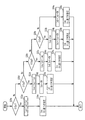
図1(a)および図1(b)は、実施例1に係るレーザドライバが用いられる光源のブロック図である。図1(a)に示すように、光源30は、複数の半導体レーザ18aから18c、複数のレーザドライバ10aから10c、およびコード生成部16を備えている。複数の半導体レーザ18aから18cは、アノードが電源にカソードがレーザドライバ10aから10cに接続されている。レーザドライバ10aから10cは、それぞれ半導体レーザ18aから18cに駆動電流Iopを供給する。コード生成部16は画像の輝度(レベル)データに基づいた輝度コードを生成する。ここで、光源30が有する複数の半導体レーザ18a、18bおよび18c、はそれぞれ赤(R)、緑(G)および青(B)の3色の半導体レーザである。半導体レーザ18a、18bおよび18cそれぞれをドライブするレーザドライバ10a、10bおよび10cに対して、コード生成部16は、各色の輝度レベルに対応した輝度コードであるカラーコードCR、CGおよびCBを生成し、各レーザドライバ10a、10bおよび10cに出力する。カラーコードCR、CGおよびCBは画像データ内のピクセルのRGBに対応する。
FIGS. 1A and 1B are block diagrams of a light source in which the laser driver according to the first embodiment is used. As shown in FIG. 1A, the
レーザドライバ10aから10cは、各半導体レーザ18aから18cにカラーコードCR、CGおよびCBに対応する駆動電流IopR、IopGおよびIopBを供給する。半導体レーザ18aから18cは、それぞれ駆動電流IopR、IopGおよびIopBに対応する光出力パワーの赤色レーザ光(波長:610nm〜660nm程度)、緑色レーザ光(波長:515nm〜540nm程度)および青色レーザ光(波長:440nm〜480nm程度)を出射する。
The
図1(b)は、3つの半導体レーザ18aから18cおよび3つのレーザドライバ10aから10cのうち1つを半導体レーザ18およびレーザドライバ10として図示している。レーザドライバ10は、駆動回路12、電流調整部14およびコード生成部16を備えている。コード生成部16は、図1(a)のように、複数のレーザドライバ10aから10cに対し設けられていてもよいし、図1(b)のように、レーザドライバ10内に設けられていてもよい。駆動回路12は、コード生成部16が生成したカラーコードCR、CGおよびCBのうち対応するカラーコードCに基づき電流Idを生成する。電流Idの方向は半導体レーザ18のダイオードの順方向である。電流調整部14は、カラーコードCに基づき半導体レーザ18に補正電流Isを生成する。電流IdとIsとは逆方向である。電流IdとIsとはノードNにおいて合成される。これにより、半導体レーザ18には、駆動電流Iopとして電流Id−Isが供給される。
FIG. 1B illustrates one of the three
[半導体レーザのI−L特性]
半導体レーザ18のI−L特性について説明する。図2(a)および図2(b)は、実施例1における半導体レーザのI−L特性を示す図である。図2(b)は、図2(a)の範囲Aの拡大図である。横軸が半導体レーザ18に供給される順方向の駆動電流Iop、駆動回路12が出力する電流IdおよびカラーコードCであり、縦軸が半導体レーザ18の光出力パワーである。I−L曲線60を太実線で示す。
[IL Characteristics of Semiconductor Laser]
The IL characteristics of the
図2(a)に示すように、駆動電流Iopが0Aのとき、光出力パワーPはほぼ0Wである。駆動電流Iopが0から大きくなっても光出力パワーPはほぼ0である。駆動電流Iopがある電流を越えると光出力パワーPが大きくなりはじめる。その後、光出力パワーPは駆動電流Iopに対し増加する。駆動電流Iopと光出力パワーPとの近似直線62を破線で示す。近似直線62が光出力パワーP=0の軸と交わる駆動電流Iopが閾値電流Ithである。図2(b)に示すように、駆動電流Iopが電流値Ith1以下では、I−L曲線60の光出力パワーPは近似直線62より大きくなる。このように、駆動電流Iopが電流値Ith1以下ではI−L特性の非線形性が大きくなる。
As shown in FIG. 2A, when the drive current Iop is 0 A, the optical output power P is almost 0 W. Even if the drive current Iop increases from 0, the optical output power P is almost 0. When the drive current Iop exceeds a certain current, the optical output power P starts to increase. Thereafter, the optical output power P increases with respect to the drive current Iop. An approximate
光源30を画像生成に用いる場合、カラーコードCと光出力パワーPとはほぼ比例することが求められる。半導体レーザ18を光出力パワーが大きな範囲で用いる場合、駆動回路12がカラーコードCに対し電流Idを線形的に出力するように設定すれば、カラーコードCと光出力パワーPはほぼ比例する。カラーコードCに対し電流Idを線形的に設定する駆動回路12は回路構成が単純であり小型化できる。
When the
半導体レーザ18を光出力パワーの小さな範囲で用いる場合、I−L特性が非線形な範囲(電流値Ith1以下の範囲)の影響が大きくなる。そこで、カラーコードCと駆動電流Iopとの関係をテーブルに記憶しておき、駆動回路12にカラーコードCが入力されると、駆動回路12はテーブルから駆動電流Iopに対応するデータを取得し出力することが考えられる。しかし、例えばカラーコードCが10ビットの場合1024階調分のカラーコードCと駆動電流Iopとのテーブルを記憶するため記憶容量の大きなメモリが必要になる。また、駆動回路12が補正式等を用いカラーコードCから駆動電流Iopを算出することが考えられる。しかし、駆動回路12の回路規模が大きくなってしまう。
When the
そこで、実施例1では、カラーコードC0のとき駆動回路12が出力する電流Idをほぼ閾値電流Ithとする。カラーコードCmaxのとき、駆動回路12が出力する電流Idを光出力パワーPがPmaxとなる電流Imaxとする。I−L曲線60が近似直線62から外れる電流値Ith1に相当するカラーコードCをコードCth1とする。駆動回路12はカラーコードCに対し線形的な電流Idを生成する。電流調整部14は、カラーコードCがコードCth1以下のとき補正電流Isを生成し、カラーコードCがコードCthより大きいとき補正電流Isを生成しない(例えば補正電流Isを0Aとする)。
Therefore, in the first embodiment, the current Id output from the
[電流調整部の制御]
電流調整部14の制御について説明する。図3は、実施例1における電流調整部の処理を示すフローチャートである。図3に示すように、電流調整部14は、コード生成部16からカラーコードCを取得する(ステップS10)。電流調整部14は、カラーコードCが所定コードCth1以下か判定する(ステップS12)。Yesのとき、電流調整部14は、電流調整を行う(ステップS14)。すなわち、電流調整部14は、電流Idと逆方向の補正電流Isを生成する。ステップS12においてNoのとき、電流調整部14は電流調整を行わない(ステップS16)。すなわち、電流調整部14は補正電流Isを生成しない(例えばIsを0Aとする)。その後終了し、ステップS10に戻り次のカラーコードCを取得する。
[Control of current adjustment unit]
Control of the
駆動回路12および電流調整部14の制御について具体的に説明する。
The control of the
[駆動回路が生成する電流の説明]
図4(a)は、実施例1におけるカラーコードCと電流Idとの関係を示す図である。ドットがカラーコードCと駆動回路12が出力する電流Idとの関係を示す点であり、破線直線65はドットを接続した線である。図4(a)に示すように、カラーコードCと電流Idとは比例関係にある。例えば、カラーコードC0からC6はそれぞれ電流Id0からId6に対応し、カラーコードCmaxはカラーコードCの最大値であり、電流Imaxに対応する。カラーコードCが10ビットの場合、カラーコードC0は0でありカラーコードCmaxは1023である。
[Description of Current Generated by Drive Circuit]
FIG. 4A is a diagram illustrating a relationship between the color code C and the current Id in the first embodiment. The dots are points indicating the relationship between the color code C and the current Id output by the
図4(b)は、実施例1における電流IdおよびカラーコードCと光出力パワーPとの関係を示す図である。ドットは各カラーコードC(すなわち駆動回路12の出力する電流Id)における目標とする光出力パワーPを示す点である。破線直線64はドットを接続した線である。図4(b)に示すように、カラーコードCがC0からC6のとき、電流IdはそれぞれId0からId6である。隣接するカラーコードC間の電流Idの間隔ΔIdはほぼ等間隔である。カラーコードC0からC6のとき目標とする光出力パワーPはそれぞれP1からP6である。光出力パワーP0は例えば0Wである。隣接するカラーコードCに対応する光出力パワーの間隔ΔPはほぼ等間隔である。
FIG. 4B is a diagram illustrating a relationship between the current Id and the color code C and the optical output power P in the first embodiment. The dot is a point indicating the target optical output power P in each color code C (that is, the current Id output from the drive circuit 12). The
実施例1では、図4(a)および図4(b)のように、カラーコードCと駆動回路12が出力する電流Idとの関係を線形的な関係(すなわち直線関係)にする。カラーコードCと電流Idが線形的な関係の場合、駆動回路12の回路規模を小さくできる。
In the first embodiment, as shown in FIGS. 4A and 4B, the relationship between the color code C and the current Id output from the
[電流調整部が生成する電流の説明]
図5は、実施例1における駆動電流Iop、電流IdおよびカラーコードCと光出力パワーPとの関係を示す図である。図3のステップS14において、電流調整部14が生成する補正電流Isを矢印で示している。図5に示すように、例えばカラーコードC1のとき、駆動回路12は電流Id1(図4(b)参照)を出力する。このとき、光出力パワーPの目標はP1であるが、実際の光出力パワーPは、I−L曲線60上のA点の光出力パワー(Pa)となり、目標のP1より大きくなってしまう。そこで、電流調整部14は、補正電流Is1を生成する。補正電流Is1をId1に合成すると駆動電流Iopは電流I1=Id1−Is1となる。これにより、カラーコードC1のときの光出力パワーPはほぼ目標のP1となり、つまり、破線直線64上のB点の位置の光出力パワーP1となり、カラーコードCに対して線形性のある光出力パワーで半導体レーザ18を点灯させることができる。
[Description of current generated by current adjusting unit]
FIG. 5 is a diagram illustrating the relationship between the drive current Iop, the current Id, the color code C, and the optical output power P in the first embodiment. In step S14 of FIG. 3, the correction current Is generated by the
同様に、カラーコードC2からC6のとき、電流調整部14は、それぞれ補正電流Is2からIs6を生成する。これにより、駆動電流I2からI6はそれぞれId2−Is2からId6−Is6となり、光出力パワーPはそれぞれ目標とするP2からP6となる。すなわち、このような電流補正を行うことによって、カラーコードC2からC6に対して、光出力パワーPがP2からP6となるので、カラーコードCに対して線形性のある(比例関係となる)光出力パワーPを得ることができる。言い換えると、カラーコードCを変化させ、その変化に応じて電流補正を行うことによって、光出力パワーPを線形的に変化させることができる。カラーコードC0のとき、目標とする光出力パワーP0が有限な値の場合、カラーコードC1からC6と同様に、電流調整部14は補正電流Is0を生成する。目標とする光出力パワーP0が0Wの場合、電流調整部14は駆動回路12の電流Idを0Aとしてもよい。
Similarly, for the color codes C2 to C6, the
[電流調整部の例]
図6は、実施例1における電流調整部の例を示すブロック図である。図6に示すように、電流調整部14は、複数の電流生成回路20aから20e、制御回路22およびメモリ24を備えている。電流生成回路20aから20eは、それぞれ補正電流IsaからIseを生成する。補正電流IsaからIseが合成された電流が補正電流Isである。制御回路22は、カラーコードCに基づいて電流生成回路20aから20eに補正電流IsaからIseを生成させる。メモリ24は、カラーコードCに基づいて補正電流IsaからIseを生成するためのパラメータ等を記憶する。
[Example of current adjustment unit]
FIG. 6 is a block diagram illustrating an example of a current adjustment unit according to the first embodiment. As shown in FIG. 6, the
図7は、実施例1におけるカラーコードCに対する補正電流Isを示す図である。図7に示すように、電流調整部14は、図3のステップS14においてカラーコードCに対応し補正電流Isを生成する。図5におけるカラーコードCに対する補正電流Is1からIs6を理想的な補正電流Isとし、図7において点線曲線68で表す。実施例1では、補正電流Isが0およびIa1からIa5となるカラーコードCをそれぞれCa0からCa5とする。点線曲線68を5個の直線66で近似する。0とIa1との間の補正電流Isは電流生成回路20aの生成する補正電流Isaに対応する。Ia1とIa2との間の補正電流Isは電流生成回路20bが生成する補正電流Isbに対応する。以下、同様に、Ia2とIa3との間、Ia3とIa4との間、およびIa4とIa5との間の補正電流Isはそれぞれ電流生成回路20cから20eの生成する補正電流IscからIseに対応する。電流生成回路20aから20eが各々生成する最大の電流値をIsmとする。この例では各補正電流IsaからIseの最大の電流値Ismは互いにほぼ同じである。各補正電流IsaからIseの最大の電流値は互いに異なっていてもよい。
FIG. 7 is a diagram illustrating the correction current Is for the color code C in the first embodiment. As shown in FIG. 7, the
図8は、実施例1において制御回路22が実行する処理を示すフローチャートであり、図3のステップS14の処理に対応する。図8に示すように、制御回路22はカラーコードCがCa1より小さいか判定する(ステップS30e)。Yesのとき、制御回路22は、補正電流IsaからIsdを一定のIsmに設定する(ステップS32e)。制御回路22は、補正電流IseをカラーコードCに線形的に対応する電流値とする(ステップS36e)。その後終了する。
FIG. 8 is a flowchart illustrating a process executed by the
ステップS30eにおいてNoのとき、制御回路22はカラーコードCがCa2より小さいか判定する(ステップS30d)。Yesのとき、制御回路22は、補正電流IsaからIscをIsmに設定し(ステップS32d)、補正電流Iseを0Aに設定し(ステップS34d)、補正電流IsdをカラーコードCに線形的に対応する電流値とする(ステップS36d)。その後終了する。
If No in step S30e, the
ステップS30dにおいてNoのとき、制御回路22はカラーコードCがCa3より小さいか判定する(ステップS30c)。Yesのとき、制御回路22は、補正電流IsaおよびIsbをIsmに設定し(ステップS32c)、補正電流IsdおよびIseを0Aに設定し(ステップS34c)、補正電流IscをカラーコードCに線形的に対応する電流値とする(ステップS36c)。その後終了する。
If No in step S30d, the
ステップS30cにおいてNoのとき、制御回路22はカラーコードCがCa4より小さいか判定する(ステップS30b)。Yesのとき、制御回路22は、補正電流IsaをIsmに設定し(ステップS32b)、補正電流IscからIseを0Aに設定し(ステップS34b)、補正電流IsbをカラーコードCに線形的に対応する電流値とする(ステップS36b)。その後終了する。
If No in step S30c, the
ステップS30bにおいてNoのとき、制御回路22は、補正電流IsbからIseを0Aに設定し(ステップS34a)、補正電流IsaをカラーコードCに線形的に対応する電流値とする(ステップS36a)。その後終了する。
If No in step S30b, the
制御回路22は、電流生成回路20aから20eが生成する補正電流IsaからIseをカラーコードCに基づきIsmまたは0にする制御、および補正電流IsaからIseをカラーコードCに対し線形にする制御を行えばよい。カラーコードCと生成する補正電流IsaからIseとが線形的な関係の場合、制御回路22の回路規模を小さくできる。また、記憶するパラメータの個数を少なくできる。さらに、カラーコードCに基づき補正電流IsaからIseをIsmまたは0Aとする制御を行う場合、制御回路22の回路規模を小さくできる。また、記憶するパラメータの個数を少なくできる。よって、電流調整部14の回路規模を小さくできる。制御回路22は、専用の論理回路を用いて実現してもよいし、プロセッサがプログラムと協働し実現してもよい。
The
[実施例1の変形例1]
図9は、実施例1の変形例1に係るレーザドライバが用いられる光源のブロック図である。図9に示すように、レーザドライバ10は電流遮断部26を備えている。電流遮断部26は、専用の論理回路を用いて実現してもよいし、プロセッサがプログラムと協働し実現してもよい。その他の構成は図1(b)と同じであり説明を省略する。
[
FIG. 9 is a block diagram of a light source in which the laser driver according to the first modification of the first embodiment is used. As shown in FIG. 9, the
図10は、実施例1の変形例1における電流遮断部および電流調整部の処理を示すフローチャートである。図10に示すように、ステップS10の後に、電流遮断部26は、カラーコードCが、Cth1より小さい所定のコードCth2以下か判定する(ステップS18)。Yesのとき、電流遮断部26は、駆動回路12および電流調整部14に駆動電流Iopを遮断させる(ステップS20)。例えば電流Idおよび補正電流Isを0Aとする。その後終了する。ステップS18においてNoのとき、ステップS12に進む。その他のフローは図3と同じであり説明を省略する。
FIG. 10 is a flowchart illustrating a process of the current interrupting unit and the current adjusting unit according to the first modification of the first embodiment. As shown in FIG. 10, after step S10, the current interrupting
図11は、実施例1の変形例1における駆動電流Iop、電流IdおよびカラーコードCと光出力パワーPとの関係を示す図である。図11に示すように、Cth1より小さいCth2を例えばC2とする。このときの電流IdはIth2である。電流調整部14は、カラーコードCがC0からC2のとき、駆動電流Iopを0Aとする。例えば電流調整部14は、電流IdおよびIsを0Aとする。これにより、カラーコードC0からC2のとき光出力パワーPは0Wとなる。その他は図5と同じであり説明を省略する。
FIG. 11 is a diagram illustrating a relationship between the drive current Iop, the current Id, the color code C, and the optical output power P in the first modification of the first embodiment. As shown in FIG. 11, Cth2 smaller than Cth1 is assumed to be C2, for example. The current Id at this time is Ith2. When the color code C ranges from C0 to C2, the
光出力パワーPが小さい領域では、駆動電流Iopに対する光出力パワーPの関係が不安定である。そこで、実施例1の変形例1のように、カラーコードCが所定コードCth2以下のとき駆動電流Iopを遮断する。これにより、意図しない光出力パワーとなることを抑制できる。 In a region where the light output power P is small, the relationship between the drive current Iop and the light output power P is unstable. Therefore, as in the first modification of the first embodiment, when the color code C is equal to or less than the predetermined code Cth2, the drive current Iop is cut off. Thereby, it is possible to suppress an unintended optical output power.
実施例1およびその変形例によれば、コード生成部16は、半導体レーザ18を駆動させるためのカラーコードC(輝度コード)を生成する。駆動回路12は、カラーコードCに基づいて、半導体レーザ18を駆動する電流Id(駆動電流)を生成する。電流調整部14は、カラーコードCの変化に応じて、半導体レーザ18の光出力パワーP(光出力強度)が線形的に変化するように、電流Idを補正する補正電流Isを生成する。電流調整部14は、カラーコードCがコードCth1(第1閾値)以下であるとき、電流Idを補正する補正電流Isを生成する。これにより、駆動回路12はカラーコードCに基づいて電流Idを生成するため駆動回路12を小型化できる。電流調整部14は、カラーコードCがコードCth1以下のとき、電流Idを補正する補正電流Isを生成する。これにより、カラーコードC全体にわたりカラーコードCに対し非線形な駆動電流を生成する場合に比べ、回路規模を小さくできる。
According to the first embodiment and its modification, the
電流調整部14は、カラーコードCがCth1より大きいとき、補正電流Isを生成しない。これにより、回路規模をより小さくできる。
When the color code C is larger than Cth1, the
Cth1が大きすぎると回路規模が大きくなってしまう。このため、Cth1はカラーコードCの最大値のカラーコードCmaxの1/2以下が好ましく、1/4以下がより好ましい。Cth1が小さすぎると、電流調整部14を用いる意味が薄くなる。よって、Cth1はCmaxの1/100以上が好ましく1/20以上がより好ましい。
If Cth1 is too large, the circuit scale will increase. For this reason, Cth1 is preferably 1 / or less, and more preferably 1 / or less, of the maximum value of the color code Cmax of the color code C. If Cth1 is too small, the meaning of using the
電流調整部14は、入力されたカラーコードCがCth1以下であるとき、入力されたカラーコードCに対応する補正電流Is(第2電流)を電流Idから減じる。これにより、駆動電流Iopを調整できる。
When the input color code C is equal to or smaller than Cth1, the
図6から図8のように、電流調整部14は、各々がカラーコードCに線形的に対応する補正電流IsaからIse(第2電流)を生成する複数の電流生成回路20aから20eを備えている。電流調整部14は、入力されたカラーコードCがCth1以下であるとき、複数の電流生成回路20aから20eが出力した補正電流IsaからIseを合成し電流Idから減じる。これにより、駆動電流Iopを調整できる。電流生成回路20aから20eの個数は適宜設定できる。
As shown in FIGS. 6 to 8, the
また、制御回路22は、入力されたカラーコードCがCth1以下であるとき、Cth1以下であるカラーコードCのうち連続するコードの範囲において、複数の電流生成回路20aから20eのうち1つの電流生成回路(例えば22c)のみに電流を生成(例えばIsc)させる。制御回路22(制御部)は、他の電流生成回路(例えば22a、22b、22dおよび22e)に入力されたカラーコードCに基づき最大の電流値Ismまたは0を出力させる。これにより、複数の電流生成回路20aから20eをカラーコードCに対し線形に制御すればよいため、制御回路22の回路規模を小さくできる。
Further, when the input color code C is equal to or less than Cth1, the
実施例1の変形例1のように、電流調整部14(電流遮断部)は、入力されたカラーコードCがCth1より小さいCth2(第2閾値)以下であるとき、駆動電流Iopを遮断する。これにより、光出力パワーPの小さい領域で光出力パワーが不安定となることを抑制できる。 As in the first modification of the first embodiment, the current adjusting unit 14 (current interrupting unit) interrupts the driving current Iop when the input color code C is equal to or smaller than Cth2 (second threshold) smaller than Cth1. This makes it possible to suppress the optical output power from becoming unstable in a region where the optical output power P is small.
光源30は、実施例1およびその変形例のレーザドライバ10と、レーザドライバ10により駆動されレーザ光を出射する半導体レーザ18と、を備えている。これにより、カラーコードCと半導体レーザ18の光出力パワーとの線形性が得ることができ、かつレーザドライバ10を小型化できる。
The
実施例1およびその変形例では、カラーコードに基づく、3色カラー表示の構成による光出力パワーの補正について説明したが、単色の光源や、赤外線(IR:infrared)などの不可視の光源において、光出力パワーの補正を行ってもよい。 In the first embodiment and its modifications, the correction of the light output power by the configuration of the three-color display based on the color code has been described. However, the light output power may be reduced by using a monochromatic light source or an invisible light source such as an infrared ray (IR). The output power may be corrected.
図12は、実施例2に係る画像投影装置のブロック図である。図12に示すように、画像投影装置100は、光源30、走査ミラー32、反射ミラー34、投影ミラー36、制御部38および画像入力部40を備えている。
FIG. 12 is a block diagram of the image projection apparatus according to the second embodiment. As shown in FIG. 12, the
画像投影装置100は、例えば眼鏡型のヘッドマウントディスプレイである。光源30は、例えば図1(a)および図1(b)に図示した光源であり、例えば眼鏡のツルに設置されている。投影ミラー36は、例えば眼鏡のレンズとしても機能する。制御部38および画像入力部40は、例えばツルに設けられている。制御部38および画像入力部40は、ヘッドマウントディスプレイに設けられずに外部装置(例えば携帯端末)に設けられていてもよい。
The
画像入力部40は、図示しないカメラおよび/または録画機器などから画像データが入力される。制御部38は、画像データに基づき光源30を制御する。制御部38は、例えばプロセッサがプログラムと協働し処理を行ってもよい。制御部38は、専用に設計された回路でもよい。
The
光源30は、レーザ光50として、例えばRGB(赤・緑・青)それぞれのレーザ光を出射する。また光源30は1つの光源であり単一の波長のレーザ光を出射してもよい。
The
走査ミラー32は、例えばMEMS(Micro Electro Mechanical Systems)であり、レーザ光50を2次元に走査する。走査されたレーザ光52は反射ミラー34に反射され投影ミラー36に照射される。
The
投影ミラー36は、ユーザの眼球42の正面に配置され、正の集光パワーを有している。投影ミラー36は、レーザ光52を水晶体46内または近傍に収束させ、網膜44近傍に合焦させる。これにより、網膜44に画像が投影される。
The
光源30は、図1(a)に示した光源であり、3色の半導体レーザ18aから18cと、半導体レーザ18aから18cを駆動するレーザドライバ10aから10cを備えている。
The
図13(a)から図13(c)は、実施例2におけるカラーコードCに対する半導体レーザの光出力パワーPを示す図である。図13(a)から図13(c)は、例えば半導体レーザ18aから18cに対応する。破線曲線70はレーザドライバ10aから10cの電流調整部14が補正電流Isを生成しないときのカラーコードCに対する光出力パワーPを示し、実線直線72は電流調整部14が補正電流Isを生成するときのカラーコードCに対する光出力パワーPを示す。
FIGS. 13A to 13C are diagrams illustrating the optical output power P of the semiconductor laser with respect to the color code C according to the second embodiment. FIGS. 13A to 13C correspond to, for example, the
半導体レーザ18aから18cのI−L特性が異なることがある。例えば、図3(a)および図3(b)における近似直線62の傾き、閾値電流IthおよびI−L曲線60が非線形となる電流値Ith1が半導体レーザ18aから18cにより異なる。
The IL characteristics of the
図13(a)から図13(c)のように、レーザドライバ10aから10cの電流調整部14が補正電流Isを生成しないと、破線曲線70のように、カラーコードCに対する光出力パワーPの非線形の度合いは半導体レーザ18aから18cで異なる。例えば、破線曲線70が非線形となるCth1および/またはCが0のときのPが半導体レーザ18aから18cで異なる。このとき、輝度の低く光出力パワーが低い画素では色ずれが発生しやすい。例えば、図13(a)から図13(c)の例では、半導体レーザ18cの非線形性が小さい。このため、カラーコードCが0付近では半導体レーザ18cの光出力パワーは半導体レーザ18aおよび18bの光出力パワーに比べ小さくなる。このため、光出力パワーが低い画素では色ずれが発生しやすくなる。
As shown in FIGS. 13A to 13C, unless the
そこで、レーザドライバ10aから10cの電流調整部14は、実施例1およびその変形例1のレーザドライバ10のように、独立に補正電流Isを生成し電流Idを補正する。これにより、図13(a)から図13(c)の実線直線72のように、半導体レーザ18aから18cのカラーコードCに対する光出力パワーPはほぼ直線となる。よって、色ずれ等を抑制できる。
Therefore, the
実施例2によれば、画像投影装置100は、実施例1およびその変形例の光源30を有する。走査ミラー32(走査部、スキャナ)は、光源30が出射したレーザ光50を走査する。投影ミラー36(画像投影部、プロジェクタ)は、走査されたレーザ光52を画像として網膜44に投影する。このような画像投影装置100では、網膜44にレーザ光52を照射する。このため、安全性の観点から半導体レーザが出力するレーザ光の光出力パワーを小さくすることが求められる。よって、I−L特性が非線形の領域を用いることになる。そこで、実施例1およびその変形例のレーザドライバを用いる。これによりレーザドライバを小型化できる。
According to the second embodiment, the
実施例2によれば、図1(a)のように、光源30はレーザドライバ10aから10c(レーザドライバ)および半導体レーザ18aから18cを各々複数備えている。図13(a)から図13(c)のように、複数のレーザドライバ10aから10c内の電流調整部14は、各々、カラーコードCがコードCth1以下であるとき、複数の半導体レーザ18aから18cのうち対応する半導体レーザのカラーコードCに対する光出力パワーPが線形性を有するように、補正電流Isを生成する。これにより、色ずれ等を抑制できる。
According to the second embodiment, as shown in FIG. 1A, the
光源30はレーザドライバ10aから10cおよび半導体レーザ18aから18cを各々3種備えている。3種の半導体レーザ18aから18cは、それぞれ赤、緑および青のレーザ光を発生する。コード生成部16は、輝度コードとして、それぞれ赤、緑および青のカラーコードを生成する。これにより、色ずれ等をより抑制できる。
The
画像投影装置100として、ヘッドマウントディスプレイを例に説明したが、画像投影装置100は視覚検査装置でもよい。実施例1およびその変形例に係るレーザドライバは、画像投影装置以外に用いてもよい。
Although the head mounted display has been described as an example of the
以上、本発明の実施例について詳述したが、本発明はかかる特定の実施例に限定されるものではなく、特許請求の範囲に記載された本発明の要旨の範囲内において、種々の変形・変更が可能である。 As described above, the embodiments of the present invention have been described in detail. However, the present invention is not limited to the specific embodiments, and various modifications and changes may be made within the scope of the present invention described in the appended claims. Changes are possible.
10、10a−10c レーザドライバ
12 駆動回路
14 電流調整部
16 コード生成部
18、18a−18c 半導体レーザ
20a−20e 電流生成回路
22 制御回路
24 メモリ
30 光源
32 走査ミラー
34 反射ミラー
36 投影ミラー
42 眼球
44 網膜
46 水晶体
10, 10a-
Claims (10)
前記輝度コードに基づいて、前記半導体レーザを駆動する駆動電流を生成する駆動回路と、
前記輝度コードの変化に応じて、前記半導体レーザの光出力強度が線形的に変化するように、前記駆動電流を補正する補正電流を生成する電流調整部と、を備え、
前記電流調整部は、前記輝度コードが第1閾値以下であるとき、前記駆動電流を補正する補正電流を生成するレーザドライバ。 A code generation unit that generates a luminance code for driving the semiconductor laser,
A drive circuit that generates a drive current for driving the semiconductor laser based on the luminance code;
A current adjusting unit that generates a correction current for correcting the drive current, so that the light output intensity of the semiconductor laser linearly changes in accordance with the change in the luminance code.
A laser driver configured to generate a correction current for correcting the drive current when the luminance code is equal to or less than a first threshold.
前記レーザドライバにより駆動されレーザ光を出射する半導体レーザと、
を備える光源。 A laser driver according to any one of claims 1 to 6,
A semiconductor laser driven by the laser driver to emit laser light;
A light source.
前記光源が出射したレーザ光を走査する走査部と、
前記走査されたレーザ光を画像として網膜に投影する画像投影部と、
を備える画像投影装置。 A light source according to claim 7,
A scanning unit that scans the laser light emitted by the light source,
An image projection unit that projects the scanned laser light as an image onto the retina,
An image projection device comprising:
前記複数のレーザドライバ内の電流調整部は、各々、前記輝度コードが前記第1閾値以下であるとき、前記複数の半導体レーザのうち対応する半導体レーザの輝度コードに対する光出力強度が線形性を有するように、補正電流を生成する、請求項8記載の画像投影装置。 The light source includes a plurality of the laser driver and the semiconductor laser, respectively,
The current adjustment units in the plurality of laser drivers each have a linear light output intensity with respect to a brightness code of a corresponding semiconductor laser among the plurality of semiconductor lasers when the brightness code is equal to or less than the first threshold. 9. The image projection device according to claim 8, wherein the correction current is generated as described above.
前記3種の半導体レーザは、それぞれ赤、緑および青のレーザ光を発生し、
前記コード生成部は、輝度コードとして、それぞれ赤、緑および青のカラーコードを生成する、請求項9記載の画像投影装置。 The light source includes three types of the laser driver and the semiconductor laser, respectively.
The three types of semiconductor lasers generate red, green, and blue laser beams, respectively.
The image projection device according to claim 9, wherein the code generation unit generates red, green, and blue color codes as luminance codes, respectively.
Priority Applications (1)
| Application Number | Priority Date | Filing Date | Title |
|---|---|---|---|
| JP2018121164A JP2020004802A (en) | 2018-06-26 | 2018-06-26 | Laser driver, light source, and image projection device |
Applications Claiming Priority (1)
| Application Number | Priority Date | Filing Date | Title |
|---|---|---|---|
| JP2018121164A JP2020004802A (en) | 2018-06-26 | 2018-06-26 | Laser driver, light source, and image projection device |
Publications (1)
| Publication Number | Publication Date |
|---|---|
| JP2020004802A true JP2020004802A (en) | 2020-01-09 |
Family
ID=69100449
Family Applications (1)
| Application Number | Title | Priority Date | Filing Date |
|---|---|---|---|
| JP2018121164A Pending JP2020004802A (en) | 2018-06-26 | 2018-06-26 | Laser driver, light source, and image projection device |
Country Status (1)
| Country | Link |
|---|---|
| JP (1) | JP2020004802A (en) |
Citations (9)
| Publication number | Priority date | Publication date | Assignee | Title |
|---|---|---|---|---|
| JPS63143887A (en) * | 1986-12-08 | 1988-06-16 | Ricoh Co Ltd | Semiconductor laser driving circuit |
| US5323408A (en) * | 1992-07-21 | 1994-06-21 | Alcatel N.V. | Regulation of preconduction current of a laser diode using the third derivative of the output signal |
| JPH10200179A (en) * | 1997-01-16 | 1998-07-31 | Konica Corp | Semiconductor laser device |
| JPH11112438A (en) * | 1997-10-02 | 1999-04-23 | Kokusai Electric Co Ltd | Analog light transmission circuit and its control method |
| JP2000200941A (en) * | 1998-12-29 | 2000-07-18 | Konica Corp | Semiconductor laser drive circuit |
| JP2004288869A (en) * | 2003-03-20 | 2004-10-14 | Fuji Xerox Co Ltd | Light emitting element driving apparatus |
| JP2007245691A (en) * | 2006-03-20 | 2007-09-27 | Seiko Epson Corp | Electro-optic device, electronic equipment, and drive method |
| JP2011508427A (en) * | 2007-12-21 | 2011-03-10 | マイクロビジョン,インク. | Laser diode compensation method and apparatus |
| JP2017194623A (en) * | 2016-04-22 | 2017-10-26 | ミツミ電機株式会社 | Display device |
-
2018
- 2018-06-26 JP JP2018121164A patent/JP2020004802A/en active Pending
Patent Citations (9)
| Publication number | Priority date | Publication date | Assignee | Title |
|---|---|---|---|---|
| JPS63143887A (en) * | 1986-12-08 | 1988-06-16 | Ricoh Co Ltd | Semiconductor laser driving circuit |
| US5323408A (en) * | 1992-07-21 | 1994-06-21 | Alcatel N.V. | Regulation of preconduction current of a laser diode using the third derivative of the output signal |
| JPH10200179A (en) * | 1997-01-16 | 1998-07-31 | Konica Corp | Semiconductor laser device |
| JPH11112438A (en) * | 1997-10-02 | 1999-04-23 | Kokusai Electric Co Ltd | Analog light transmission circuit and its control method |
| JP2000200941A (en) * | 1998-12-29 | 2000-07-18 | Konica Corp | Semiconductor laser drive circuit |
| JP2004288869A (en) * | 2003-03-20 | 2004-10-14 | Fuji Xerox Co Ltd | Light emitting element driving apparatus |
| JP2007245691A (en) * | 2006-03-20 | 2007-09-27 | Seiko Epson Corp | Electro-optic device, electronic equipment, and drive method |
| JP2011508427A (en) * | 2007-12-21 | 2011-03-10 | マイクロビジョン,インク. | Laser diode compensation method and apparatus |
| JP2017194623A (en) * | 2016-04-22 | 2017-10-26 | ミツミ電機株式会社 | Display device |
Similar Documents
| Publication | Publication Date | Title |
|---|---|---|
| JP4582179B2 (en) | Image display device | |
| JP5640420B2 (en) | Projection-type image display device | |
| US8067725B2 (en) | Device and method for displaying image | |
| US7959303B2 (en) | Image display device | |
| US10944945B2 (en) | Projection device and projection method, projection module, electronic device, and program | |
| JP6649148B2 (en) | Laser projection display device | |
| JP5956949B2 (en) | Image display device | |
| US8767023B2 (en) | Scanning image display device and method of controlling the same | |
| JP5316346B2 (en) | Retina scanning image display device | |
| CN108693649B (en) | Display device | |
| US11056031B2 (en) | Control device, optical scanner, display device, and control method | |
| US11146764B2 (en) | Control device, optical scanning device, display apparatus, and control method | |
| JP2012053279A (en) | Color image forming apparatus, color image forming method, and projector including the color image forming apparatus | |
| JP2020004802A (en) | Laser driver, light source, and image projection device | |
| WO2014162414A1 (en) | Projection device, head-up display, control method, program, and storage medium | |
| US11997432B2 (en) | Display apparatus | |
| JP2016099561A (en) | Projection device, projection method, program, and storage medium | |
| KR102210710B1 (en) | Layer display device and operation method thereof | |
| JP2014059522A (en) | Image display device | |
| US20230388462A1 (en) | Control device, control method, control program, and projection apparatus | |
| JP6721082B2 (en) | Projection apparatus, projection method, program and storage medium | |
| JP6961910B2 (en) | Optical axis correction device, control method, program and storage medium | |
| JP2021149005A (en) | Video display device, head-up display device, and moving body |
Legal Events
| Date | Code | Title | Description |
|---|---|---|---|
| A621 | Written request for application examination |
Free format text: JAPANESE INTERMEDIATE CODE: A621 Effective date: 20210114 |
|
| A977 | Report on retrieval |
Free format text: JAPANESE INTERMEDIATE CODE: A971007 Effective date: 20211222 |
|
| A131 | Notification of reasons for refusal |
Free format text: JAPANESE INTERMEDIATE CODE: A131 Effective date: 20220105 |
|
| A521 | Request for written amendment filed |
Free format text: JAPANESE INTERMEDIATE CODE: A523 Effective date: 20220210 |
|
| A131 | Notification of reasons for refusal |
Free format text: JAPANESE INTERMEDIATE CODE: A131 Effective date: 20220524 |
|
| A02 | Decision of refusal |
Free format text: JAPANESE INTERMEDIATE CODE: A02 Effective date: 20221122 |