JP2020002441A - Facing target sputtering film deposition apparatus - Google Patents
Facing target sputtering film deposition apparatus Download PDFInfo
- Publication number
- JP2020002441A JP2020002441A JP2018124237A JP2018124237A JP2020002441A JP 2020002441 A JP2020002441 A JP 2020002441A JP 2018124237 A JP2018124237 A JP 2018124237A JP 2018124237 A JP2018124237 A JP 2018124237A JP 2020002441 A JP2020002441 A JP 2020002441A
- Authority
- JP
- Japan
- Prior art keywords
- targets
- target
- sputtering
- film forming
- frequency power
- Prior art date
- Legal status (The legal status is an assumption and is not a legal conclusion. Google has not performed a legal analysis and makes no representation as to the accuracy of the status listed.)
- Granted
Links
Images


Abstract
Description
本発明は、スパッタリングによって成膜を行う装置に関し、特に一対のスパッタリングターゲット(以下、適宜「ターゲット」という。)を対向させて高周波電源を用いて放電させることにより成膜を行うスパッタ成膜装置の技術に関する。 The present invention relates to an apparatus for forming a film by sputtering, and more particularly to a sputter film forming apparatus for forming a film by discharging using a high frequency power supply with a pair of sputtering targets (hereinafter, appropriately referred to as “targets”) facing each other. About technology.
近年、種々のデバイス(半導体、電子、ディスプレイ、太陽電池など)の高性能化、微細化が進んでいる。
このようなデバイスを製造するには、真空中においてパーティクルの発生が少なく高品質な薄膜形成技術が重要である。
In recent years, various devices (semiconductors, electronics, displays, solar cells, and the like) have been improved in performance and miniaturization.
In order to manufacture such a device, a high-quality thin film forming technique that generates few particles in a vacuum is important.
かかる薄膜形成技術としては、従来より、マグネトロン式スパッタリング装置と対向ターゲット式スパッタリング装置が知られている。
しかし、マグネトロン式スパッタリング装置では、成膜中に高い運動エネルギーを持った粒子が基板表面に衝突し膜質の低下を引き起こすという問題がある。
As such a thin film forming technique, a magnetron type sputtering apparatus and a facing target type sputtering apparatus are conventionally known.
However, the magnetron sputtering apparatus has a problem in that particles having high kinetic energy collide with the substrate surface during film formation and cause deterioration in film quality.
これに対し、対向ターゲット式スパッタリング装置は、一対のターゲットが対向し基板はその側方に設置する構造であるため、成膜中に高い運動エネルギーを持った粒子が基板表面に衝突するのを抑制することでができ、これにより高品質の薄膜を形成することができる。 On the other hand, the facing target type sputtering device has a structure in which a pair of targets face each other and the substrate is set on the side of the target, so that particles having high kinetic energy during the film formation are prevented from colliding with the substrate surface. Thus, a high-quality thin film can be formed.
しかし、対向ターゲット式スパッタリング装置は、ターゲットが対向する構造であるため、ターゲット表面に非エロージョン領域が存在すると、この非エロージョン領域に膜が堆積し、その結果、長期間にわたって使用すると、非エロージョン領域から膜が剥離し、パーティクルが発生するという問題がある。 However, the facing target type sputtering apparatus has a structure in which the target faces each other. Therefore, when a non-erosion region exists on the target surface, a film is deposited on the non-erosion region. There is a problem that the film is peeled off from the substrate and particles are generated.
従来の対向ターゲット式スパッタリング装置では、対向するターゲットの背面側に設置した永久磁石が形成する磁場構造によりターゲットの中心部分がスパッタされる一方、ターゲットの縁部近傍には全くスパッタされないためターゲットの縁部に非エロージョン領域が形成される。
したがって、パーティクルの発生を抑制するためには、ターゲット表面に非エロージョン領域が発生しないように放電させることが重要である。
In a conventional facing target type sputtering apparatus, the center portion of the target is sputtered by a magnetic field structure formed by a permanent magnet installed on the back side of the facing target, but the target edge is not sputtered at all near the edge of the target. A non-erosion region is formed in the portion.
Therefore, in order to suppress the generation of particles, it is important to discharge so that a non-erosion region is not generated on the target surface.
これに対し、従来、ターゲットの非エロージョン領域の表面に防着板を設置してパーティクルの発生を抑制する技術も提案されている(例えば特許文献1参照)。
しかし、この従来技術の防着板はプラズマの影響で加熱され易く、かつ、構造的に冷却しにくいため、成膜時と非成膜時の熱サイクルにより防着板が熱膨張と収縮を繰り返し、その結果、長期的に使用するとパーティクルが発生するという問題がある。
On the other hand, conventionally, a technique has been proposed in which a deposition plate is provided on the surface of a non-erosion region of a target to suppress generation of particles (for example, see Patent Document 1).
However, since this conventional deposition-preventing plate is easily heated by the influence of plasma and is structurally difficult to cool, the deposition-preventing plate repeatedly undergoes thermal expansion and contraction due to thermal cycles during film formation and non-film formation. As a result, there is a problem that particles are generated when used for a long time.
本発明は、このような従来の技術の課題を考慮してなされたもので、その目的とするところは、対向ターゲット式スパッタ成膜装置において、ターゲット表面における非エロージョン領域の発生を阻止し、非エロージョン領域の膜剥がれによるパーティクルの発生を抑制する技術を提供することにある。 The present invention has been made in consideration of such problems of the related art, and an object of the present invention is to prevent the generation of a non-erosion region on a target surface in a facing target type sputtering film forming apparatus. An object of the present invention is to provide a technique for suppressing generation of particles due to peeling of a film in an erosion region.
上記目的を達成するためになされた本発明は、接地された真空槽内で一対のスパッタリングターゲットを対向させてスパッタ成膜を行う対向ターゲット式スパッタ成膜装置であって、第1及び第2のカソード電極と、前記第1及び第2のカソード電極に電気的にそれぞれ接続され、放電空間を挟んで対向配置される第1及び第2のスパッタリングターゲットと、前記第1及び第2のカソード電極の背面側で前記第1及び第2のスパッタリングターゲットの縁部に対応する位置に、前記放電空間を挟んで異なる磁極が対向するようにそれぞれ配置された第1及び第2の磁石装置と、前記第1及び第2のカソード電極の電力供給端子と前記真空槽の接地端子との間にそれぞれ高周波電力を供給する高周波電源とを備え、前記第1及び第2のスパッタリングターゲットの周囲をそれぞれ近接して取り囲むように、当該第1及び第2のスパッタリングターゲットのターゲット表面との間の結合容量がそれぞれ調整された第1及び第2のアノード電極が設けられているものである。
本発明では、前記第1及び第2のアノード電極は、前記第1及び第2のスパッタリングターゲットのターゲット表面側の部分に凹凸が設けられていることも効果的である。
本発明では、前記第1及び第2のスパッタリングターゲットのターゲット表面に対する第1及び第2のアノード電極の表面の角度がそれぞれ−45°以上90°以下となるように構成されていることも効果的である。
本発明では、前記第1及び第2のスパッタリングターゲットと前記第1及び第2のアノード電極との間にそれぞれ所定の厚さの絶縁体が設けられていることも効果的である。
本発明では、前記第1及び第2のカソード電極に対してそれぞれ13.56MHz以上100MHz以下の高周波電力を供給するように構成されていることも効果的である。
本発明では、前記第1及び第2のカソード電極の中央部に対してそれぞれ前記高周波電力を供給するように構成されていることも効果的である。
本発明では、前記第1及び第2のカソード電極に対してそれぞれ直流電力を更に供給するように構成されていることも効果的である。
本発明では、前記第1及び第2のカソード電極に高周波電力を供給した場合において当該第1及び第2のカソード電極の各部分のインピーダンスを調整するインピーダンス調整手段がそれぞれ設けられていることも効果的である。
The present invention made in order to achieve the above object is a facing target type sputtering film forming apparatus for performing sputtering film formation with a pair of sputtering targets facing each other in a grounded vacuum chamber. A cathode electrode, first and second sputtering targets electrically connected to the first and second cathode electrodes, respectively, and opposed to each other with a discharge space interposed therebetween; A first and a second magnet device arranged at positions corresponding to the edges of the first and second sputtering targets on the back side so that different magnetic poles face each other across the discharge space; A high-frequency power supply for supplying high-frequency power between power supply terminals of the first and second cathode electrodes and a ground terminal of the vacuum chamber, respectively; A first and a second anode electrodes, each of which has a coupling capacity between the first and second sputtering targets and a target surface thereof, respectively, so as to surround the ring target in close proximity to each other. It is.
In the present invention, it is also effective that the first and second anode electrodes are provided with irregularities on the target surface side of the first and second sputtering targets.
In the present invention, it is also effective that the angles of the surfaces of the first and second anode electrodes with respect to the target surfaces of the first and second sputtering targets are respectively −45 ° or more and 90 ° or less. It is.
In the present invention, it is also effective that an insulator having a predetermined thickness is provided between the first and second sputtering targets and the first and second anode electrodes, respectively.
In the present invention, it is also effective that the first and second cathode electrodes are configured to supply high-frequency power of 13.56 MHz to 100 MHz, respectively.
In the present invention, it is also effective that the high-frequency power is supplied to the central portions of the first and second cathode electrodes, respectively.
In the present invention, it is also effective that DC power is further supplied to each of the first and second cathode electrodes.
According to the present invention, it is also advantageous that, when high-frequency power is supplied to the first and second cathode electrodes, impedance adjusting means for adjusting the impedance of each portion of the first and second cathode electrodes are provided. It is a target.
本発明にあっては、対向ターゲット式スパッタ成膜装置において、第1及び第2のカソード電極の背面側で第1及び第2のスパッタリングターゲットの縁部に対応する位置にそれぞれ第1及び第2の磁石装置が放電空間を挟んで配置され、第1及び第2のスパッタリングターゲットの周囲をそれぞれ近接して取り囲むように、第1及び第2のスパッタリングターゲットのターゲット表面との間の結合容量がそれぞれ調整されたアノード電極が設けられているため、第1及び第2のスパッタリングターゲットに対して高周波電力(例えば13.56MHz以上100MHz以下)を供給した場合に、一対のスパッタリングターゲットの中央部分の間、並びに、一対のスパッタリングターゲットの縁部と一対のアノード電極との間においてそれぞれ放電を生じさせることができる。 According to the present invention, in the facing target type sputtering film forming apparatus, the first and second sputtering targets are located on the back side of the first and second cathode electrodes at positions corresponding to the edges of the first and second sputtering targets, respectively. Are disposed so as to sandwich the discharge space, and the coupling capacities between the target surfaces of the first and second sputtering targets are respectively set so as to surround the first and second sputtering targets in close proximity to each other. Since the adjusted anode electrode is provided, when high-frequency power (for example, 13.56 MHz or more and 100 MHz or less) is supplied to the first and second sputtering targets, between the central portions of the pair of sputtering targets, In addition, each between the edge of the pair of sputtering targets and the pair of anode electrodes It is possible to cause the discharge.
その結果、本発明によれば、各スパッタリングターゲットにおいて全面的に放電が生じスパッタリングが行われるため、各スパッタリングターゲットのターゲット表面における非エロージョン領域の発生を阻止し、非エロージョン領域の膜剥がれによるパーティクルの発生を抑制することができる。 As a result, according to the present invention, discharge is generated over the entire surface of each sputtering target and sputtering is performed, so that generation of non-erosion regions on the target surface of each sputtering target is prevented, and particles due to film peeling of non-erosion regions are prevented. Generation can be suppressed.
また、本発明によれば、各スパッタリングターゲットの全面をエロージョン領域とすることができるので、スパッタリングターゲットの使用効率を向上させることができる。 Further, according to the present invention, the entire surface of each sputtering target can be an erosion region, so that the use efficiency of the sputtering target can be improved.
さらに、従来、例えば金属ターゲットを用いて酸素や窒素ガスを用いた反応性スパッタにおいて、成膜速度を高く保つためターゲットのターゲット表面をメタルの状態を保ちつつ、基板表面に酸化膜、窒化膜もしくは酸窒化膜を形成する方法が知られている(メタルモードスパッタ)が、その際、ターゲットのターゲット表面に非エロージョン部分が存在するとその表面には酸化膜、窒化膜もしくは酸窒化膜が堆積することがあり、この膜が絶縁性の場合、放電時にArイオンがチャージされた絶縁膜が形成されてしまう。 Furthermore, conventionally, for example, in a reactive sputtering using oxygen or nitrogen gas using a metal target, an oxide film, a nitride film or A method of forming an oxynitride film is known (metal mode sputtering). At this time, if a non-erosion portion exists on the target surface of the target, an oxide film, a nitride film, or an oxynitride film is deposited on the surface. When this film is insulating, an insulating film charged with Ar ions at the time of discharge is formed.
この場合、所定量のチャージが溜まると絶縁膜に絶縁破壊が生じイオン電流が絶縁膜から金属ターゲットに流れるか、メタル状態のエロージョン部に流れ、これにより異常放電が発生する。 In this case, when a predetermined amount of charge accumulates, dielectric breakdown occurs in the insulating film, and an ionic current flows from the insulating film to the metal target or to the erosion portion in a metal state, thereby causing abnormal discharge.
しかし、本発明によれば、各スパッタリングターゲットにおいて全面的に放電が生じスパッタリングが行われるため、上述した異常放電を防止することができる。 However, according to the present invention, since the entire discharge is generated in each sputtering target and the sputtering is performed, the abnormal discharge described above can be prevented.
本発明において、第1及び第2のアノード電極の第1及び第2のスパッタリングターゲットのターゲット表面側の部分に凹凸が設けられている場合、第1及び第2のスパッタリングターゲットのターゲット表面に対する第1及び第2のアノード電極の表面の角度がそれぞれ−45°以上90°以下となるように構成されている場合、又は第1及び第2のスパッタリングターゲットと第1及び第2のアノード電極との間に所定の厚さの絶縁体が設けられている場合には、第1及び第2のアノード電極と第1及び第2のスパッタリングターゲットのターゲット表面との間の結合容量をそれぞれ容易に調整することができる。 In the present invention, when the first and second anode electrodes are provided with irregularities on portions of the first and second sputtering targets on the target surface side, the first and second sputtering targets have a first surface with respect to the target surface. And when the angle of the surface of the second anode electrode is -45 ° or more and 90 ° or less, respectively, or between the first and second sputtering targets and the first and second anode electrodes. In the case where an insulator having a predetermined thickness is provided, the coupling capacity between the first and second anode electrodes and the target surfaces of the first and second sputtering targets can be easily adjusted. Can be.
本発明において、第1及び第2のカソード電極に高周波電力を供給した場合において第1及び第2のカソード電極の各部分のインピーダンスを調整するインピーダンス調整手段がそれぞれ設けられている場合には、第1及び第2のスパッタリングターゲットのターゲット表面との間の結合容量がそれぞれ調整されたアノード電極による作用と相俟って第1及び第2のスパッタリングターゲットの各部分においてそれぞれ均一に放電させることができ、これにより第1及び第2のスパッタリングターゲットの縁部の各部分とアノード電極間においてもそれぞれ均一に放電させることができる。 In the present invention, when high-frequency power is supplied to the first and second cathode electrodes, and when impedance adjusting means for adjusting the impedance of each portion of the first and second cathode electrodes is provided, In combination with the operation of the anode electrode whose coupling capacity between the first and second sputtering targets and the target surface is adjusted, it is possible to uniformly discharge the respective portions of the first and second sputtering targets. Thereby, it is possible to uniformly discharge between each of the edge portions of the first and second sputtering targets and the anode electrode.
以下、本発明の実施の形態を図面を参照して詳細に説明する。
図1は、本発明に係る対向ターゲット式スパッタ成膜装置の内部構成を示す概略図である。
Hereinafter, embodiments of the present invention will be described in detail with reference to the drawings.
FIG. 1 is a schematic diagram showing the internal configuration of a facing target type sputtering film forming apparatus according to the present invention.
図1に示すように、本実施の形態の対向ターゲット式スパッタ成膜装置1は、成膜対象物である基板15が配置される例えば箱形状の真空成膜室2を有している。
As shown in FIG. 1, a facing target type sputtering
この真空成膜室2は、例えばその一方側の部分に、図示しない真空排気装置に接続された排気部2aと、アルゴンガスを含むプロセスガスを導入するためのガス導入部2bが設けられている。
また、真空成膜室2は、その外壁部に設けられた接地端子2dを介して接地されている。
The vacuum
The vacuum
真空成膜室2の例えば上記排気部2a及びガス導入部2bが設けられた側と反対側の部分には、真空成膜室2の開口部2c側に取り付けられ、高周波が外部の空間に発散するのを抑制する高周波シールドカバー部3が設けられている。
For example, a portion of the vacuum
高周波シールドカバー部3内には、基本的な構成が同一である一対の第1及び第2のスパッタ部4A、4Bが、真空成膜室2と連通され真空成膜室2と同等の真空雰囲気が維持されるように設けられた放電空間21を挟んで設けられている。
Inside the high-frequency shield cover 3, a pair of first and
本実施の形態の第1のスパッタ部4Aと第2のスパッタ部4Bは、それぞれターゲット部を構成する筐体20A、20Bに組み付けられた第1及び第2のターゲット5A、5Bを含む複数の部材を有し、第1及び第2のターゲット5A、5Bのスパッタ面が対向して平行になるように配置されている。
The
本発明においては、上述した真空成膜室2と、第1及び第2のスパッタ部4A、4Bの筐体20A、20Bによって真空槽が構成されている。
In the present invention, a vacuum chamber is formed by the above-described vacuum
ここで、第1及び第2のターゲット5A、5Bは、同一の材料(例えば酸化物)からなり、本例ではそれぞれ円板形状に形成されている。そして、第1及び第2のターゲット5A、5Bは、それぞれのスパッタ面が基板15の成膜面に対して垂直になるように、カソード電極である第1及び第2のバッキングプレート6A、6Bにそれぞれ取り付けられている。
Here, the first and
第1及び第2のターゲット5A、5Bの周囲には、導電性の金属材料(例えばアルミニウムを主成分とする合金)からなる第1及び第2のアノード電極7A、7Bが、第1及び第2のターゲット5A、5B及び第1及び第2のバッキングプレート6A、6Bを取り囲むようにそれぞれ設けられている。本例の第1及び第2のアノード電極7A、7Bは、それぞれ円形リング状に形成されている。
Around the first and
これら第1及び第2のアノード電極7A、7Bは、絶縁体70によって第1及び第2のターゲット5A、5B、第1及び第2のバッキングプレート6A、6Bに対してそれぞれ電気的に絶縁され、真空成膜室2の外壁部と電気的に接続されている。
These first and
さらに、第1及び第2のアノード電極7A、7Bは、第1及び第2のバッキングプレート6A、6Bを取り囲むように設けられ絶縁性材料からなるフランジ部材8A、8Bによっても第1及び第2のバッキングプレート6A、6Bに対してそれぞれ電気的に絶縁されている。
Further, the first and
この場合、第1及び第2のアノード電極7A、7Bは、それぞれの内周部が、絶縁体70を介して第1及び第2のターゲット5A、5Bの外周部と近接するように配置されている。
In this case, the first and
そして、第1及び第2のアノード電極7A、7Bは、後述するように、第1及び第2のターゲット5A、5Bのターゲット表面との間の結合容量がそれぞれ調整された状態になるように構成されている。
The first and
第1及び第2のスパッタ部4A、4Bには、第1及び第2のバッキングプレート6A、6Bの第1及び第2のターゲット5A、5Bのスパッタ面と反対側の即ち背面側の部分に、例えば永久磁石からなる第1及び第2の磁石装置9A、9Bがそれぞれヨーク板10A、10Bに取り付けられて固定されている。
In the first and
これら第1及び第2の磁石装置9A、9Bは、第1及び第2のターゲット5A、5Bの縁部に沿う形状(例えば円形リング形状)に形成され、放電空間21を挟んで異なる極性の部分が対向するように配置されている。
These first and
このような構成により、第1及び第2のターゲット5A、5B間の放電空間21においては、第1及び第2のターゲット5A、5Bの縁部に沿う形状、本例では後述する円筒形状の対向磁場が生成される。
With such a configuration, the
一方、高周波シールドカバー部3の外部には、高周波電源22が設けられ、この高周波電源22において発生させた高周波電力を、マッチングボックス23を介して第1及び第2のスパッタ部4A、4Bの第1及び第2のバッキングプレート6A、6Bにそれぞれ供給するように構成されている。
On the other hand, a high-
本実施の形態の場合は、第1及び第2のバッキングプレート6A、6Bの中央部の第1及び第2の電力供給端子6a、6bに対してそれぞれ高周波電力を供給する。
In the case of the present embodiment, high-frequency power is supplied to the first and second
本発明の場合、第1及び第2のバッキングプレート6A、6Bに供給する高周波電力の周波数は特に限定されることはないが、第1及び第2のターゲット5A、5Bの縁部を確実にスパッタリングする観点からは、13.56MHz以上とすることが好ましく、より好ましくは、27MHz以上100MHz以下である。
In the case of the present invention, the frequency of the high frequency power supplied to the first and
高周波電力の周波数が13.56MHzより小さいと、DC電源を用いた場合と同様に第1及び第2のターゲット5A、5Bの縁部に生成される高周波プラズマの密度が小さいため、スパッタリングの速度より膜が堆積する速度の方が大きくなってしまう。
When the frequency of the high-frequency power is smaller than 13.56 MHz, the density of the high-frequency plasma generated at the edges of the first and
一方、高周波電力の周波数が100MHzより大きい場合には、第1及び第2のターゲット5A、5Bの縁部に生成される高周波プラズマの密度が大きくなると、第1及び第2のバッキングプレート6A、6Bに供給する高周波電力が同高周波プラズマを経由して第1及び第2のアノード電極7A、7Bに流れやすくなる。そのため、ターゲット中央部分に対して高周波電力が届かなくなり、プラズマ密度が低下し、スパッタリングの速度より膜が堆積する速度の方が大きくなってしまう。
On the other hand, when the frequency of the high-frequency power is higher than 100 MHz, when the density of the high-frequency plasma generated at the edges of the first and
すなわち、本発明では、供給する高周波電力の周波数により、第1及び第2のターゲット5A、5Bの中央部分/縁部におけるスパッタリング速度を調整する。
That is, in the present invention, the sputtering rate at the center / edge of the first and
また、本発明では、特に限定されることはないが、第1及び第2のバッキングプレート6A、6Bに対し、それぞれ高周波電力に直流電力を更に重畳して供給するように構成することもできる。
Further, in the present invention, although not particularly limited, the first and
すなわち、第1及び第2のバッキングプレート6A、6Bに対して供給する高周波電力の周波数が大きくなるに従い、第1及び第2のターゲット5A、5Bの縁部に生成される高周波プラズマの密度が大きくなり、第1及び第2のターゲット5A、5Bに印加される直流電圧成分(VDC)が小さくなるため、スパッタリングのレートが低下する問題が生ずる場合がある。
That is, as the frequency of the high-frequency power supplied to the first and
そこで、第1及び第2のバッキングプレート6A、6Bに対し、それぞれ高周波電力に直流電力を更に重畳して供給することによって、供給する高周波電力の周波数を大きくした場合であっても、スパッタリングのレートの低下を防止することができる。
Therefore, even when the frequency of the supplied high-frequency power is increased by supplying DC power to the first and
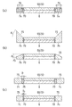
図2(a)〜(c)は、第1及び第2のアノード電極7A、7Bの表面(放電空間側の面)と、第1及び第2のターゲット5A、5Bのターゲット表面(放電空間側の面)との間の結合容量をそれぞれ調整する手段を模式的に示す説明図である。
FIGS. 2A to 2C show surfaces of the first and
以下、図2(a)〜(c)では、上記第1及び第2のターゲット5A、5Bをターゲット5とし、上記第1及び第2のバッキングプレート6A、6Bをバッキングプレート6とし、上記第1及び第2のアノード電極7A、7Bをアノード電極7a〜7cとして包括的に説明する。
Hereinafter, in FIGS. 2A to 2C, the first and
まず、図2(a)に示す例は、アノード電極7aに、例えばアノード電極7aの表面7Sに、凹凸としてアノード電極7aの表面7Sに対して直交する方向に延びる複数の穴部71を形成したものである。
First, in the example shown in FIG. 2A, a plurality of
これら穴部71の開口形状は、円形状、四角形状、多角形状等とすることができる。
また、穴部71内の壁部にプラズマが確実に接触することを考慮すると、穴部71の開口径は、例えば円形状の場合に5mm以上に設定することが好ましい。
The opening shape of these
In consideration of the fact that the plasma contacts the wall inside the
本例は、アノード電極7aの表面7Sに対して直交する方向に延びる複数の穴部71を形成することによって、アノード電極7aの表面7Sの面積が、当該穴部71を形成しない場合に比べて大きくなるように構成したものである。
In this example, by forming a plurality of
このような構成を有する本例では、アノード電極7aの表面7Sと、カソード電極であるバッキングプレート6に電気的に接続されたターゲット5のターゲット表面5Sとの間の結合容量が当該穴部71を形成しない場合に比べて大きくなり、これによってアノード電極7aの表面7Sとターゲット5のターゲット表面5Sとの間のインピーダンスが相対的に小さくなる。
In the present example having such a configuration, the coupling capacity between the
その結果、本例によれば、ターゲット5のターゲット表面5Sからアノード電極7aの表面7Sに高周波電力が流れやすくなり、ターゲット5の縁部に生成される高周波プラズマの密度を向上させることができる。
As a result, according to the present example, high-frequency power easily flows from the
なお、本例では、アノード電極7aに設ける穴部71の開口面積、深さ並びに穴部71の個数を調整することにより、アノード電極7aの表面7Sの面積を調整してターゲット5の縁部に生成される高周波プラズマの密度を最適の値に調整することができる。
In this example, by adjusting the opening area and depth of the
図2(b)に示す例は、ターゲット5のターゲット表面5Sに対するアノード電極7bの表面7Sの角度を変えるようにしたものである。
この場合、ターゲット5のターゲット表面5Sに対するアノード電極7bの表面7Sの角度が0°より大きい場合(θ1)には、アノード電極7bの表面7Sとターゲット5のターゲット表面5Sとの間の距離がターゲット5のターゲット表面5Sに対するアノード電極7bの表面7Sの角度が0°の場合に比べて小さくなるため、アノード電極7bの表面7Sとターゲット5のターゲット表面5Sとの間の結合容量が相対的に大きくなり、これによってアノード電極7bの表面7Sとターゲット5のターゲット表面5Sとの間のインピーダンスが相対的に小さくなる。
In the example shown in FIG. 2B, the angle of the
In this case, when the angle of the
その結果、ターゲット5のターゲット表面5Sからアノード電極7bの表面7Sに高周波電力が流れやすくなり、ターゲット5の縁部に生成される高周波プラズマの密度が増加する。
As a result, high-frequency power easily flows from the
一方、ターゲット5のターゲット表面5Sに対するアノード電極7bの表面7Sの角度が0°より小さい場合(θ2)には、アノード電極7bの表面7Sとターゲット5のターゲット表面5Sとの間の距離がターゲット5のターゲット表面5Sに対するアノード電極7bの表面7Sの角度が0°の場合に比べて大きくなるため、アノード電極7bの表面7Sとターゲット5のターゲット表面5Sとの間の結合容量が相対的に小さくなり、これによってアノード電極7bの表面7Sとターゲット5のターゲット表面5Sとの間のインピーダンスが相対的に大きくなる。
On the other hand, when the angle of the
その結果、ターゲット5のターゲット表面5Sからアノード電極7bの表面7Sに高周波電力が流れにくくなり、ターゲット5の縁部に生成される高周波プラズマの密度が減少する。
As a result, it becomes difficult for high-frequency power to flow from the
本発明の場合、特に限定されることはないが、ターゲット5のターゲット表面5Sに対するアノード電極7bの表面7Sの角度が−45°以上90°以下となるように構成すれば、ターゲット5の縁部に生成される高周波プラズマの密度を最適の値に調整することができる。
In the case of the present invention, although not particularly limited, if the angle of the
図2(c)に示す例は、ターゲット5とアノード電極7cとの間に設けられた絶縁体70の厚さを変えるようにしたものである。
この場合、ターゲット5とアノード電極7cとの間に設けられた絶縁体70の厚さを小さくすると(D1>D2)、アノード電極7cの表面7Sとターゲット5のターゲット表面5Sとの間の距離が小さくなるため、アノード電極7cの表面7Sと、カソード電極であるバッキングプレート6に電気的に接続されたターゲット5のターゲット表面5Sとの間の結合容量が相対的に大きくなり、これによってアノード電極7cの表面7Sとターゲット5のターゲット表面5Sとの間のインピーダンスが相対的に小さくなる。
In the example shown in FIG. 2C, the thickness of the
In this case, when the thickness of the
その結果、ターゲット5のターゲット表面5Sからアノード電極7cの表面7Sに高周波電力が流れやすくなり、ターゲット5の縁部に生成される高周波プラズマの密度を向上させることができる。
As a result, high-frequency power easily flows from the
このように、本例では、ターゲット5とアノード電極7cとの間に設けられた絶縁体70の厚さを調整することにより、アノード電極7cの表面7Sとターゲット5のターゲット表面5Sとの間の距離を調整してターゲット5の縁部に生成される高周波プラズマの密度を最適の値に調整することができる。
Thus, in this example, by adjusting the thickness of the
本発明の場合、特に限定されることはないが、ターゲット5とアノード電極7との間に設けられる絶縁体の厚さを3mm以上50mm以下とすることにより、ターゲットの縁部に生成される高周波プラズマの密度を最適の値に調整することができる。
In the case of the present invention, the thickness of the insulator provided between the
なお、図2(a)〜(c)を参照して記載した、アノード電極7の表面7Sと、ターゲット5のターゲット表面5Sとの間の結合容量を調整する手段は、組み合わせて構成することもできる。
The means for adjusting the coupling capacitance between the
図3(a)(b)は、本発明の原理を説明するための図で、図3(a)は本実施の形態の磁気回路によって発生した磁場(磁束)の分布を模式的に示す説明図、図3(b)は本実施の形態において生成されたプラズマの分布を模式的に示す説明図である。 3A and 3B are diagrams for explaining the principle of the present invention, and FIG. 3A is a diagram schematically illustrating a distribution of a magnetic field (magnetic flux) generated by the magnetic circuit according to the present embodiment. FIG. 3B is an explanatory diagram schematically showing the distribution of the plasma generated in the present embodiment.
図3(a)に示すように、本実施の形態では、第1のスパッタ部4Aの第1の磁石装置9AのN極と、第2のスパッタ部4Bの第2の磁石装置9BのS極が対向するように配置されている。
As shown in FIG. 3A, in the present embodiment, the N pole of the
これにより、本実施の形態では、第1の磁石装置9Aから第2の磁石装置9Bに向かう方向の磁力線を有する対向磁場30が発生する。この対向磁場30は、第1のターゲット5A及び第2のターゲット5Bの縁部をそれぞれ貫くように形成される。
As a result, in the present embodiment, an opposing
上述したように、第1及び第2の磁石装置9A、9Bは円形リング状に形成されているから、発生した対向磁場30は、放電空間21内において円筒形状に形成される。
As described above, since the first and
また、第1のスパッタ部4Aでは、第1の磁石装置9Aのリングの内側に、そのN極からS極へ向かう方向の第1のマグネトロン磁場31が発生する。
一方、第2のスパッタ部4Bでは、第2の磁石装置9Bのリングの内側に、そのN極からS極へ向かう方向の第2のマグネトロン磁場32が発生する。
In the
On the other hand, in the
このような磁場が形成された状態において、真空下の真空成膜室2内にプロセスガスを導入し、高周波電源22にて発生させた高周波電力をマッチングボックス23を介して第1及び第2のスパッタ部4A、4Bの第1及び第2のバッキングプレート6A、6Bの中央部の第1及び第2の電力供給端子6a、6bにそれぞれ供給すると、これらの高周波電力は、表皮効果によりそれぞれ第1及び第2のバッキングプレート6A、6Bの縁部及び第1及び第2のターゲット5A、5Bの縁部を介して第1及び第2のターゲット5A、5Bのスパッタ面の中央部分に向って流れる。
In a state where such a magnetic field is formed, a process gas is introduced into the vacuum
その結果、第1のターゲット5Aと、第2のターゲット5Bの間の放電空間21において放電が生じ、図3(b)に示すように、第1及び第2のターゲット5A、5Bの中央部分において対向プラズマ35が生成される。
As a result, a discharge is generated in the
この対向プラズマ35は、第1の磁石装置9Aと第2の磁石装置9Bとの間の放電空間21において生成された円筒形状の対向磁場30によってこの対向磁場30の内側に閉じこめられた状態になる。
The
この場合、対向プラズマ35中の電子は、放電空間21内において第1及び第2のターゲット5A、5B間を往復するように飛翔する。また、第1及び第2のターゲット5A、5Bの近傍では、上述した第1及び第2のマグネトロン磁場31、32により、対向プラズマ35中の電子がそれぞれの磁力線に沿って周回するように飛翔する。
In this case, the electrons in the opposing
そして、この対向プラズマ35中のアルゴンイオンが第1及び第2のターゲット5A、5Bの中央部分に衝突することにより、第1及び第2のターゲット5A、5Bの中央部分においてスパッタリングが行われる。
Then, the argon ions in the
その一方で、上述したように、第1及び第2のバッキングプレート6A、6Bの中央部の第1及び第2の電力供給端子6a、6bにそれぞれ供給された高周波電力は、それぞれ第1及び第2のバッキングプレート6A、6Bの縁部及び第1及び第2のターゲット5A、5Bの縁部を介して第1及び第2のターゲット5A、5Bのスパッタ面の中央部分に向って流れる際に、第1及び第2のターゲット5A、5Bと、それぞれの周囲に近接配置された第1及び第2のアノード電極7A、7Bとの間においても放電が生じ、図3(b)に示すように、それぞれプラズマ36、37が生成される。
On the other hand, as described above, the high-frequency power supplied to the first and second
この場合、例えば上述した図2(a)〜(c)に示す手段を用い、第1及び第2のアノード電極7A、7Bの表面と、第1及び第2のターゲット5A、5Bの表面との間の結合容量をそれぞれ適切な値に調整することにより、プラズマ36、37のプラズマ密度を最適な状態で生成することができる。
In this case, for example, using the means shown in FIGS. 2A to 2C described above, the surface of the first and
そして、これらプラズマ36、37中のアルゴンイオンが第1及び第2のターゲット5A、5Bの縁部に衝突することにより、第1及び第2のターゲット5A、5Bの縁部においてスパッタリングが行われる。
Then, the argon ions in the
このように、本実施の形態では、第1及び第2のターゲット5A、5Bに対して高周波電力(例えば13.56MHz以上100MHz以下)を供給した場合に、第1及び第2のターゲット5A、5Bの中央部分の間、並びに、第1及び第2のターゲット5A、5Bの縁部と第1及び第2のアノード電極7A、7Bとの間においてそれぞれ放電を生じさせることができ、第1及び第2のターゲット5A、5Bにおいてそれぞれ全面的にスパッタリングが行われる。
As described above, in the present embodiment, when high-frequency power (for example, 13.56 MHz or more and 100 MHz or less) is supplied to the first and
そして、このようなスパッタリング工程を経て第1及び第2のターゲット5A、5Bから飛び出したスパッタ粒子が真空成膜室2内の基板15の表面に到達することにより、基板15の表面に第1及び第2のターゲット5A、5Bの材料の膜が形成される。
Then, the sputtered particles sputtered from the first and
以上述べた本実施の形態によれば、第1及び第2のターゲット5A、5Bの表面における非エロージョン領域の発生を阻止し、非エロージョン領域の膜剥がれによるパーティクルの発生を抑制することができる。
According to the above-described embodiment, the generation of non-erosion regions on the surfaces of the first and
ところで、上記実施の形態のように、第1及び第2のターゲット5A、5B及びこれに対応する第1及び第2のバッキングプレート6A、6Bの形状が円形の場合には、カソード電極であるバッキングプレート6A、6Bの中央部の第1及び第2の電力供給端子6a、6bに高周波電力を供給する場合、第1及び第2のターゲット5A、5Bの中央部から縁部及び第1及び第2のアノード電極7A、7Bまでの距離は第1及び第2のターゲット5A、5Bの全周にわたって等しく、このため第1及び第2のターゲット5A、5B及び第1及び第2のアノード電極7A、7Bの全周にわたって均一に放電が行われる。
Incidentally, when the first and
しかし、ターゲット及びこれに対応するバッキングプレートの形状が正方形形状や長方形形状のような矩形形状である場合には、ターゲットの中央部と縁部及びアノード電極との距離がターゲットの中央部から縁部に延びる線分の回転角度によって異なり、その結果、インピーダンスも同線分の回転角度によって異なるから、バッキングプレートの中央部に高周波電力を供給した場合には、第1及び第2のターゲット間の各部分、並びに、第1及び第2のターゲットの縁部の各部分と第1及び第2のアノード電極間において均一に放電させることができない。
具体的には、高周波電力の電力供給端子と放電部との距離が大きくなるに従いインピーダンスが大きくなり、生成されるプラズマの密度が小さくなる。
However, when the target and the corresponding backing plate have a rectangular shape such as a square shape or a rectangular shape, the distance between the center and the edge of the target and the anode electrode is changed from the center of the target to the edge. Depends on the rotation angle of the line segment extending in the direction, and as a result, the impedance also depends on the rotation angle of the line segment. Therefore, when high-frequency power is supplied to the center of the backing plate, each of the first and second targets is It is not possible to discharge uniformly between the first and second anode electrodes and the first and second anode electrodes.
Specifically, as the distance between the power supply terminal of the high-frequency power and the discharge unit increases, the impedance increases and the density of the generated plasma decreases.
そこで、本発明では、以下のような手段を採用することにより、上述した課題を解決することができる。
図4(a)(b)は、ターゲット及びバッキングプレートの形状が正方形形状の場合のインピーダンス調整手段の例を示す概略構成図である。以下、本発明の理解を容易にするために、上述した第1及び第2のスパッタ部4A、4Bのように一対のスパッタ部のうち、一方のスパッタ部を例にとって説明する。
Therefore, the present invention can solve the above-mentioned problem by employing the following means.
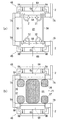
FIGS. 4A and 4B are schematic configuration diagrams showing an example of the impedance adjusting means when the target and the backing plate have a square shape. Hereinafter, in order to facilitate understanding of the present invention, one of the pair of sputtering units, such as the above-described first and
図4(a)に示す例では、正方形形状のターゲット40の背面側に正方形形状のバッキングプレート41が設けられ、これらターゲット40及びバッキングプレート41の周囲を取り囲むように正方形リング形状のアノード電極42が設けられている。
In the example shown in FIG. 4A, a
本例では、バッキングプレート41の背面側の表面に、「+」形状の高周波電力拡散部材43が設けられている。
この高周波電力拡散部材43は、例えば銅(Cu)等のバッキングプレート41と同様に導電率の小さい金属材料からなり、バッキングプレート41(ターゲット40)に対して電気的に接続されている。
In this example, a “+” shaped high-frequency
The high-frequency
ここで、高周波電力拡散部材43は、ターゲット40及びバッキングプレート41の中央部41aに対して等しい長さを有する四つの直線状の拡散部43aがそれぞれ90度の回転角度で設けられ、これら直線状の拡散部43aがバッキングプレート41の四つの隅部に向って延びるように設けられている。
Here, the high-frequency
この場合、高周波電力拡散部材43は、各拡散部43aの端部とバッキングプレート41の四つの隅部とがそれぞれ電気的に接続され、高周波電力拡散部材43のその他の部分とバッキングプレート41との間に所定の空間を設けるように構成することが好ましい。
In this case, the high-frequency
そして、ターゲット40及びバッキングプレート41の中央部41aと対応する位置に設けられた高周波電力拡散部材43の電力供給端子60aに対して高周波電力を供給するように構成されている。
Then, it is configured to supply high-frequency power to the
本例では、高周波電力拡散部材43の四つの直線状の部分は、同一の幅で形成されている。
このような構成を有する本例において高周波電力拡散部材43の電力供給端子60aに対して高周波電力を供給すると、高周波電力拡散部材43の四つの拡散部43aに沿って高周波電力が供給されるようになる。
In this example, the four linear portions of the high-frequency
In the present example having such a configuration, when high-frequency power is supplied to the
その結果、本例によれば、ターゲット40及びバッキングプレート41の中央部41aに対する距離が最も大きい各隅部に対し、より大きい高周波電力を供給することができるので、ターゲット40の各部分において均一に放電させることができ、これによりターゲット40の縁部の各部分とアノード電極42間においても均一に放電させることができる。
As a result, according to the present example, higher high-frequency power can be supplied to each corner where the distance between the
そして、他方のスパッタ部についても上記同一の構成を採用することにより、上述した作用により、第1及び第2のターゲット間の各部分、並びに、第1及び第2のターゲットの縁部の各部分と第1及び第2のアノード電極間においてそれぞれ均一に放電させることができる。 Then, by adopting the same configuration for the other sputter portion, the above-described operation allows each portion between the first and second targets and each portion of the edge of the first and second targets. And the first and second anode electrodes can be uniformly discharged.
図5(a)(b)は、ターゲット及びバッキングプレートの形状が長方形形状の場合インピーダンスの調整手段の例を示す概略構成図である。以下、理解を容易にするために、一対のスパッタ部のうち、一方のスパッタ部を例にとって説明する。 FIGS. 5A and 5B are schematic configuration diagrams showing examples of impedance adjustment means when the target and the backing plate have a rectangular shape. Hereinafter, in order to facilitate understanding, one of the pair of sputtering units will be described as an example.
図5(a)に示す例では、長方形形状のターゲット50の背面側に長方形形状のバッキングプレート51が設けられ、これらターゲット50及びバッキングプレート51の周囲を取り囲むように長方形リング形状のアノード電極52が設けられている。
In the example illustrated in FIG. 5A, a
本例では、バッキングプレート51の背面側の表面に、幅の異なる拡散部を有する高周波電力拡散部材53が設けられている。
図5(b)に示すように、本例の高周波電力拡散部材53は、長方形形状のバッキングプレート51の中央部分に、バッキングプレート51の長辺部と平行な直線状の第1の拡散部53aが設けられている。
In this example, a high-frequency
As shown in FIG. 5B, the high-frequency
そして、この第1の拡散部53aの両端部に、第1の拡散部53aと連続しバッキングプレート51の四隅に向ってそれぞれ直線状に延びる第2の拡散部53bが設けられている。
Further, at both ends of the
さらに、バッキングプレート51の中央部分には、バッキングプレート51の対向する長辺部に向ってそれぞれ直線状に延びる複数の第3の拡散部53cが設けられている。
Further, a plurality of
さらにまた、バッキングプレート51の上記第2の拡散部53bの間には、バッキングプレート51の短辺部に向ってそれぞれ直線状に延びる第4の拡散部53dが設けられている。
Further, between the
ここで、高周波電力拡散部材53は、第2の拡散部53bの端部とバッキングプレート51の四つの隅部と、第3の拡散部53cの端部とバッキングプレート51の長辺部と、第4の拡散部53dの端部とバッキングプレート51の短辺部とが電気的に接続され、高周波電力拡散部材53のその他の部分とバッキングプレート51との間には所定の空間を設けるように構成することが好ましい。
Here, the high-frequency
本例の場合、第1の拡散部53aの幅が、第3及び第4の拡散部53c、53dの幅より大きくなるようにそれぞれの寸法が設定されている。
また、第2の拡散部53bの長さが、第3及び第4の拡散部53c、53dの長さより長くなるようにそれぞれの寸法が設定されている。
In the case of this example, the respective dimensions are set such that the width of the
The respective dimensions are set such that the length of the
これは、直線状の導電性部材のインピーダンスは、その幅が小さくなるに従い大きくなること、また第1の拡散部53aからバッキングプレート51の長辺部及び短辺部に向かう方向の距離と四隅に向かう方向との距離の差を考慮し、ターゲット表面において均一に放電させるようにしたものである。
This is because the impedance of the linear conductive member increases as the width decreases, and the distance in the direction from the
このような構成を有する本例によれば、図5(a)に示すバッキングプレート51の中央部51aに対する距離が最も大きい各隅部に対し、より大きい高周波電力を供給することができるので、ターゲット50の各部分において均一に放電させることができ、これによりターゲット50の縁部の各部分とアノード電極間においても均一に放電させることができる。
According to the present example having such a configuration, a larger high-frequency power can be supplied to each corner of the
そして、他方のスパッタ部についても上記同一の構成を採用することにより、上述した作用により、第1及び第2のターゲット間の各部分、並びに、第1及び第2のターゲットの縁部の各部分と第1及び第2のアノード電極間においてそれぞれ均一に放電させることができる。 Then, by adopting the same configuration for the other sputter portion, the above-described operation allows each portion between the first and second targets and each portion of the edge of the first and second targets. And the first and second anode electrodes can be uniformly discharged.
なお、本発明は上記実施の形態に限られず、種々の変更を行うことができる。 例えば、上記実施の形態では、バッキングプレートに対して一つの電力供給端子に対して高周波電力を供給するように構成したが、本発明はこれに限られず、バッキングプレートに対して二つ以上の電力供給端子に対して高周波電力を供給することもできる。 Note that the present invention is not limited to the above embodiment, and various changes can be made. For example, in the above embodiment, the high-frequency power is supplied to one power supply terminal for the backing plate, but the present invention is not limited to this, and two or more power supplies may be supplied to the backing plate. High-frequency power can also be supplied to the supply terminal.
この場合、高周波電力を供給する位置については、バッキングプレートの中央部に限られず、例えば正方形形状のバッキングプレートでは各隅部に高周波電力を供給することもでき、また、長方形形状のバッキングプレートでは、その長手方向の両端部に高周波電力を供給することもできる。 In this case, the position for supplying the high-frequency power is not limited to the central portion of the backing plate. High-frequency power can be supplied to both ends in the longitudinal direction.
さらに、図4(a)(b)及び図5(a)(b)に示すインピーダンス調整手段に、図2(a)〜(c)に示すアノード電極7a〜7cの表面7Sとターゲット5のターゲット表面5Sとの間の結合容量を調整する手段を組み合わせることもできる。
Further, the impedance adjusting means shown in FIGS. 4A and 5B and FIGS. 5A and 5B are added to the
1……対向ターゲット式スパッタ成膜装置
2……真空成膜室
2d…接地端子
3……高周波シールドカバー部
4A…第1のスパッタ部
4B…第2のスパッタ部
5A…第1のスパッタリングターゲット
5B…第2のスパッタリングターゲット
6A…第1のバッキングプレート(第1のカソード電極)
6B…第2のバッキングプレート(第2のカソード電極)
6a…第1の電力供給端子
6b…第2の電力供給端子
7A…第1のアノード電極
7B…第2のアノード電極
9A…第1の磁石装置
9B…第2の磁石装置
15…基板
21…放電空間
1 ... opposed target type sputtering
6B: second backing plate (second cathode electrode)
6a first
Claims (8)
第1及び第2のカソード電極と、
前記第1及び第2のカソード電極に電気的にそれぞれ接続され、放電空間を挟んで対向配置される第1及び第2のスパッタリングターゲットと、
前記第1及び第2のカソード電極の背面側で前記第1及び第2のスパッタリングターゲットの縁部に対応する位置に、前記放電空間を挟んで異なる磁極が対向するようにそれぞれ配置された第1及び第2の磁石装置と、
前記第1及び第2のカソード電極の電力供給端子と前記真空槽の接地端子との間にそれぞれ高周波電力を供給する高周波電源とを備え、
前記第1及び第2のスパッタリングターゲットの周囲をそれぞれ近接して取り囲むように、当該第1及び第2のスパッタリングターゲットのターゲット表面との間の結合容量がそれぞれ調整された第1及び第2のアノード電極が設けられている対向ターゲット式スパッタ成膜装置。 A facing target type sputtering film forming apparatus that performs sputtering film formation by facing a pair of sputtering targets in a grounded vacuum chamber,
First and second cathode electrodes;
First and second sputtering targets electrically connected to the first and second cathode electrodes, respectively, and opposed to each other with a discharge space interposed therebetween;
The first and second cathode electrodes are arranged at positions corresponding to the edges of the first and second sputtering targets on the back side, respectively, such that different magnetic poles are arranged so as to face each other with the discharge space interposed therebetween. And a second magnet device;
A high-frequency power supply for supplying high-frequency power between a power supply terminal of the first and second cathode electrodes and a ground terminal of the vacuum chamber,
First and second anodes each having a controlled coupling capacity between the first and second sputtering targets and a target surface of the first and second sputtering targets so as to closely surround the first and second sputtering targets, respectively. A facing target type sputtering film forming apparatus provided with electrodes.
Priority Applications (1)
| Application Number | Priority Date | Filing Date | Title |
|---|---|---|---|
| JP2018124237A JP7102260B2 (en) | 2018-06-29 | 2018-06-29 | Opposed target type sputtering film deposition equipment |
Applications Claiming Priority (1)
| Application Number | Priority Date | Filing Date | Title |
|---|---|---|---|
| JP2018124237A JP7102260B2 (en) | 2018-06-29 | 2018-06-29 | Opposed target type sputtering film deposition equipment |
Publications (2)
| Publication Number | Publication Date |
|---|---|
| JP2020002441A true JP2020002441A (en) | 2020-01-09 |
| JP7102260B2 JP7102260B2 (en) | 2022-07-19 |
Family
ID=69098823
Family Applications (1)
| Application Number | Title | Priority Date | Filing Date |
|---|---|---|---|
| JP2018124237A Active JP7102260B2 (en) | 2018-06-29 | 2018-06-29 | Opposed target type sputtering film deposition equipment |
Country Status (1)
| Country | Link |
|---|---|
| JP (1) | JP7102260B2 (en) |
Cited By (1)
| Publication number | Priority date | Publication date | Assignee | Title |
|---|---|---|---|---|
| WO2022181434A1 (en) * | 2021-02-26 | 2022-09-01 | 株式会社フルヤ金属 | Powder surface film-forming device and method for manufacturing coated powder |
Citations (7)
| Publication number | Priority date | Publication date | Assignee | Title |
|---|---|---|---|---|
| JPH05125527A (en) * | 1991-11-05 | 1993-05-21 | Canon Inc | Sputtering method and device for forming thin magnetic film |
| JPH0734236A (en) * | 1993-07-19 | 1995-02-03 | Canon Inc | D.c. sputtering device and sputtering method |
| JPH0813143A (en) * | 1994-06-24 | 1996-01-16 | Hitachi Ltd | Plasma treatment and treating device |
| JP2000328243A (en) * | 1999-05-21 | 2000-11-28 | Ulvac Japan Ltd | Sputtering device |
| JP2009280882A (en) * | 2008-05-26 | 2009-12-03 | Panasonic Corp | Sputtering apparatus |
| JP2010156018A (en) * | 2008-12-26 | 2010-07-15 | Masahiko Naoe | Sputtering apparatus |
| JP2013079420A (en) * | 2011-10-03 | 2013-05-02 | Japan Steel Works Ltd:The | Sputtering apparatus |
-
2018
- 2018-06-29 JP JP2018124237A patent/JP7102260B2/en active Active
Patent Citations (7)
| Publication number | Priority date | Publication date | Assignee | Title |
|---|---|---|---|---|
| JPH05125527A (en) * | 1991-11-05 | 1993-05-21 | Canon Inc | Sputtering method and device for forming thin magnetic film |
| JPH0734236A (en) * | 1993-07-19 | 1995-02-03 | Canon Inc | D.c. sputtering device and sputtering method |
| JPH0813143A (en) * | 1994-06-24 | 1996-01-16 | Hitachi Ltd | Plasma treatment and treating device |
| JP2000328243A (en) * | 1999-05-21 | 2000-11-28 | Ulvac Japan Ltd | Sputtering device |
| JP2009280882A (en) * | 2008-05-26 | 2009-12-03 | Panasonic Corp | Sputtering apparatus |
| JP2010156018A (en) * | 2008-12-26 | 2010-07-15 | Masahiko Naoe | Sputtering apparatus |
| JP2013079420A (en) * | 2011-10-03 | 2013-05-02 | Japan Steel Works Ltd:The | Sputtering apparatus |
Cited By (1)
| Publication number | Priority date | Publication date | Assignee | Title |
|---|---|---|---|---|
| WO2022181434A1 (en) * | 2021-02-26 | 2022-09-01 | 株式会社フルヤ金属 | Powder surface film-forming device and method for manufacturing coated powder |
Also Published As
| Publication number | Publication date |
|---|---|
| JP7102260B2 (en) | 2022-07-19 |
Similar Documents
| Publication | Publication Date | Title |
|---|---|---|
| US20180374689A1 (en) | Electrically and Magnetically Enhanced Ionized Physical Vapor Deposition Unbalanced Sputtering Source | |
| KR20010062069A (en) | A plasma processing system for sputter deposition applications | |
| JPS60135573A (en) | Method and device for sputtering | |
| WO2017112700A1 (en) | Electrically and magnetically enhanced ionized physical vapor deposition unbalanced sputtering source | |
| JP2013206652A (en) | Antenna device, and plasma processing apparatus and sputtering apparatus having the same | |
| US20130092533A1 (en) | Sputter deposition apparatus | |
| US8617363B2 (en) | Magnetron sputtering apparatus | |
| US20110048927A1 (en) | Sputtering apparatus and sputtering method | |
| US11251020B2 (en) | Sputtering apparatus | |
| JP2009187682A (en) | Method for manufacturing cathode electrode, and method for manufacturing thin film solid lithium-ion secondary battery | |
| US8470145B2 (en) | Cathode unit and sputtering apparatus provided with the same | |
| JP5146106B2 (en) | Sputtering equipment | |
| JP2012052191A (en) | Sputtering apparatus | |
| US9028659B2 (en) | Magnetron design for extended target life in radio frequency (RF) plasmas | |
| JP4473852B2 (en) | Sputtering apparatus and sputtering method | |
| JP7102260B2 (en) | Opposed target type sputtering film deposition equipment | |
| WO2018175689A1 (en) | Magnetron sputtering source for insulating target materials | |
| JP4408987B2 (en) | Plasma processing equipment for sputter processing | |
| EP2368258B1 (en) | Rf sputtering arrangement | |
| JP2004115841A (en) | Magnetron sputtering electrode, film deposition system, and film deposition method | |
| JP2013122080A (en) | Sputtering device | |
| JP6959447B2 (en) | Sputter film forming equipment | |
| JP7114368B2 (en) | Sputtering equipment | |
| JP2009235581A (en) | High-frequency sputtering apparatus | |
| JP3562595B2 (en) | Sputtering equipment |
Legal Events
| Date | Code | Title | Description |
|---|---|---|---|
| RD03 | Notification of appointment of power of attorney |
Free format text: JAPANESE INTERMEDIATE CODE: A7423 Effective date: 20200727 |
|
| RD04 | Notification of resignation of power of attorney |
Free format text: JAPANESE INTERMEDIATE CODE: A7424 Effective date: 20200805 |
|
| A621 | Written request for application examination |
Free format text: JAPANESE INTERMEDIATE CODE: A621 Effective date: 20210511 |
|
| A977 | Report on retrieval |
Free format text: JAPANESE INTERMEDIATE CODE: A971007 Effective date: 20220228 |
|
| A131 | Notification of reasons for refusal |
Free format text: JAPANESE INTERMEDIATE CODE: A131 Effective date: 20220301 |
|
| A521 | Request for written amendment filed |
Free format text: JAPANESE INTERMEDIATE CODE: A523 Effective date: 20220428 |
|
| RD02 | Notification of acceptance of power of attorney |
Free format text: JAPANESE INTERMEDIATE CODE: A7422 Effective date: 20220428 |
|
| TRDD | Decision of grant or rejection written | ||
| A01 | Written decision to grant a patent or to grant a registration (utility model) |
Free format text: JAPANESE INTERMEDIATE CODE: A01 Effective date: 20220607 |
|
| A61 | First payment of annual fees (during grant procedure) |
Free format text: JAPANESE INTERMEDIATE CODE: A61 Effective date: 20220706 |
|
| R150 | Certificate of patent or registration of utility model |
Ref document number: 7102260 Country of ref document: JP Free format text: JAPANESE INTERMEDIATE CODE: R150 |