JP2019531464A - 三次元固体イメージング光検出器 - Google Patents
三次元固体イメージング光検出器 Download PDFInfo
- Publication number
- JP2019531464A JP2019531464A JP2019505046A JP2019505046A JP2019531464A JP 2019531464 A JP2019531464 A JP 2019531464A JP 2019505046 A JP2019505046 A JP 2019505046A JP 2019505046 A JP2019505046 A JP 2019505046A JP 2019531464 A JP2019531464 A JP 2019531464A
- Authority
- JP
- Japan
- Prior art keywords
- scintillator
- active region
- disposed
- immersive
- detector
- Prior art date
- Legal status (The legal status is an assumption and is not a legal conclusion. Google has not performed a legal analysis and makes no representation as to the accuracy of the status listed.)
- Pending
Links
Images


Classifications
-
- G—PHYSICS
- G01—MEASURING; TESTING
- G01T—MEASUREMENT OF NUCLEAR OR X-RADIATION
- G01T1/00—Measuring X-radiation, gamma radiation, corpuscular radiation, or cosmic radiation
- G01T1/16—Measuring radiation intensity
- G01T1/20—Measuring radiation intensity with scintillation detectors
- G01T1/2006—Measuring radiation intensity with scintillation detectors using a combination of a scintillator and photodetector which measures the means radiation intensity
-
- A—HUMAN NECESSITIES
- A61—MEDICAL OR VETERINARY SCIENCE; HYGIENE
- A61B—DIAGNOSIS; SURGERY; IDENTIFICATION
- A61B6/00—Apparatus for radiation diagnosis, e.g. combined with radiation therapy equipment
- A61B6/02—Devices for diagnosis sequentially in different planes; Stereoscopic radiation diagnosis
- A61B6/03—Computerised tomographs
- A61B6/032—Transmission computed tomography [CT]
-
- A—HUMAN NECESSITIES
- A61—MEDICAL OR VETERINARY SCIENCE; HYGIENE
- A61B—DIAGNOSIS; SURGERY; IDENTIFICATION
- A61B6/00—Apparatus for radiation diagnosis, e.g. combined with radiation therapy equipment
- A61B6/42—Apparatus for radiation diagnosis, e.g. combined with radiation therapy equipment with arrangements for detecting radiation specially adapted for radiation diagnosis
- A61B6/4208—Apparatus for radiation diagnosis, e.g. combined with radiation therapy equipment with arrangements for detecting radiation specially adapted for radiation diagnosis characterised by using a particular type of detector
-
- G—PHYSICS
- G01—MEASURING; TESTING
- G01N—INVESTIGATING OR ANALYSING MATERIALS BY DETERMINING THEIR CHEMICAL OR PHYSICAL PROPERTIES
- G01N23/00—Investigating or analysing materials by the use of wave or particle radiation, e.g. X-rays or neutrons, not covered by groups G01N3/00 – G01N17/00, G01N21/00 or G01N22/00
- G01N23/02—Investigating or analysing materials by the use of wave or particle radiation, e.g. X-rays or neutrons, not covered by groups G01N3/00 – G01N17/00, G01N21/00 or G01N22/00 by transmitting the radiation through the material
- G01N23/04—Investigating or analysing materials by the use of wave or particle radiation, e.g. X-rays or neutrons, not covered by groups G01N3/00 – G01N17/00, G01N21/00 or G01N22/00 by transmitting the radiation through the material and forming images of the material
- G01N23/046—Investigating or analysing materials by the use of wave or particle radiation, e.g. X-rays or neutrons, not covered by groups G01N3/00 – G01N17/00, G01N21/00 or G01N22/00 by transmitting the radiation through the material and forming images of the material using tomography, e.g. computed tomography [CT]
-
- G—PHYSICS
- G01—MEASURING; TESTING
- G01N—INVESTIGATING OR ANALYSING MATERIALS BY DETERMINING THEIR CHEMICAL OR PHYSICAL PROPERTIES
- G01N23/00—Investigating or analysing materials by the use of wave or particle radiation, e.g. X-rays or neutrons, not covered by groups G01N3/00 – G01N17/00, G01N21/00 or G01N22/00
- G01N23/02—Investigating or analysing materials by the use of wave or particle radiation, e.g. X-rays or neutrons, not covered by groups G01N3/00 – G01N17/00, G01N21/00 or G01N22/00 by transmitting the radiation through the material
- G01N23/06—Investigating or analysing materials by the use of wave or particle radiation, e.g. X-rays or neutrons, not covered by groups G01N3/00 – G01N17/00, G01N21/00 or G01N22/00 by transmitting the radiation through the material and measuring the absorption
- G01N23/083—Investigating or analysing materials by the use of wave or particle radiation, e.g. X-rays or neutrons, not covered by groups G01N3/00 – G01N17/00, G01N21/00 or G01N22/00 by transmitting the radiation through the material and measuring the absorption the radiation being X-rays
-
- G—PHYSICS
- G01—MEASURING; TESTING
- G01N—INVESTIGATING OR ANALYSING MATERIALS BY DETERMINING THEIR CHEMICAL OR PHYSICAL PROPERTIES
- G01N2223/00—Investigating materials by wave or particle radiation
- G01N2223/03—Investigating materials by wave or particle radiation by transmission
- G01N2223/04—Investigating materials by wave or particle radiation by transmission and measuring absorption
-
- G—PHYSICS
- G01—MEASURING; TESTING
- G01N—INVESTIGATING OR ANALYSING MATERIALS BY DETERMINING THEIR CHEMICAL OR PHYSICAL PROPERTIES
- G01N2223/00—Investigating materials by wave or particle radiation
- G01N2223/40—Imaging
- G01N2223/419—Imaging computed tomograph
-
- G—PHYSICS
- G01—MEASURING; TESTING
- G01N—INVESTIGATING OR ANALYSING MATERIALS BY DETERMINING THEIR CHEMICAL OR PHYSICAL PROPERTIES
- G01N2223/00—Investigating materials by wave or particle radiation
- G01N2223/50—Detectors
- G01N2223/505—Detectors scintillation
Abstract
Description
Claims (20)
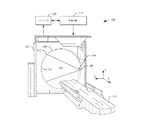
- 検出器画素であって、
活性領域を含む壁を有する三次元キャビティであって、前記三次元キャビティ内を横切る光線フォトンを検出し、それを示す各電気信号を生成する、三次元キャビティと、
少なくとも1つの検出器画素の底部に隣接して前記三次元キャビティ内に配置される第1のシンチレータと、
前記第1のシンチレータの上の前記三次元キャビティ内に配置される第2のシンチレータであって、前記第1及び第2のシンチレータがX線フォトンの吸収に応答して前記光線フォトンを放出する、第2のシンチレータと
を含み、
前記壁の少なくとも一つは前記検出器画素に対して垂直に方向付けられ、対応する活性領域と前記第1又は第2のシンチレータの一つとの間の接触面積を最大にする、
検出器画素
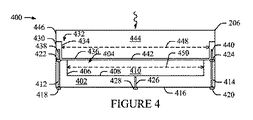
を有する、検出器アレイ。 - 前記三次元キャビティは、第1の没入部及び前記第1の没入部内の第2の没入部を含み、前記第1のシンチレータは前記第2の没入部内に配置され、前記第2のシンチレータは前記第1の没入部内に配置され、前記第1及び第2の没入部のそれぞれは、垂直に方向付けられる壁のみを含む、請求項1に記載の検出器アレイ。
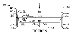
- 前記少なくとも1つの検出器画素は、前記第1のシンチレータと前記第2のシンチレータとの間に配置される光学層をさらに含む、請求項2に記載の検出器アレイ。
- 前記三次元キャビティは、第1の没入部及び前記第1の没入部内の第2の没入部を含み、前記第1のシンチレータは前記第2の没入部内に配置され、前記第2のシンチレータは前記第1の没入部内に配置され、前記第1の没入部は横方向の壁を含み、前記第2の没入部は垂直に方向付けられる壁のみを含む、請求項1に記載の検出器アレイ。
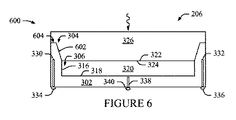
- 前記検出器画素の側面に配置される電極と、
前記活性領域から前記電極まで延在するビアと、
前記活性領域から前記電極まで前記ビア内に配置される導電経路と
を更に有する、請求項2乃至4の何れか一項に記載の検出器アレイ。 - 単一ブロックがシリコンを含む、請求項5に記載の検出器アレイ。
- 前記少なくとも1つの検出器画素は、前記第1のシンチレータが配置される第1の没入部を備える第1のブロックと、前記第2のシンチレータが配置される第2の没入部を備える第2のブロックとを含む、少なくとも2つのブロックをさらに含む、請求項1に記載の検出器アレイ。
- 前記第1及び第2のブロックは互いに結合される、請求項7に記載の検出器アレイ。
- 前記第2のブロックは第1及び第2の導電経路を含み、前記第1のブロックは第3及び第4の導電経路を含み、前記第1及び第2の導電経路は、前記第3及び第4の導電経路と電気的に接触している、請求項7乃至8の何れか一項に記載の検出器アレイ。
- 前記第1の没入部は横方向の壁を含み、前記第2の没入部は垂直に方向付けられる壁のみを含む、請求項7乃至9の何れか一項に記載の検出器アレイ。
- 前記三次元キャビティは、前記画素の中央領域に向かって前記第1の没入部内の第2の没入部へ延在する床を有する第1の没入部を含み、前記床は、前記第1及び第2の没入部の前記壁の間にレッジ領域を提供し、前記第1のシンチレータは前記第2の没入部内に配置され、前記第2のシンチレータは前記第1の没入部内に配置される、請求項1乃至10の何れか一項に記載の検出器アレイ。
- 前記第1のシンチレータは第1のX線吸収特性を有し、前記第2のシンチレータは第2のX線吸収特性を有し、前記第1及び第2のX線吸収特性は異なる、請求項1乃至10の何れか一項に記載の検出器アレイ。
- 前記第1のシンチレータは第1の放出X線吸収を有し、前記第2のシンチレータは第2のX線吸収特性を有し、前記第1及び第2のX線吸収特性は同じである、請求項1乃至10の何れか一項に記載の検出器アレイ。
- 三次元固体撮像光検出器のシンチレータを用いてX線フォトンを受け取るステップと、
前記シンチレータを用いて前記X線フォトンを吸収するステップと、
前記シンチレータを用いて、前記X線フォトンの吸収に応答して、前記X線フォトンのエネルギーを示す光線フォトンを生成するステップと、
前記三次元固体撮像光検出器の活性領域を用いて前記光線フォトンを検出するステップと
を有し、
前記シンチレータと前記活性領域との間の接触面積は最大にされ、
活性領域を用いて、前記光線フォトンの検出に応答して、前記X線フォトンの前記エネルギーを示す電気信号を生成するステップ
を有する、方法。 - 前記第1のシンチレータを用いて第1のエネルギーを有するフォトンを検出するステップと、
前記シンチレータの第2の異なる1つを用いて第2の異なるエネルギーを有するフォトンを検出するステップと、
スペクトル画像を生成するように前記電気信号を再構成するステップと
を更に有する、請求項14に記載の方法。 - X線を放出するように構成されるX線源と、
X線を検出してそれを示す信号を生成するように構成される三次元固体撮像光検出器であって、前記三次元固体撮像光検出器は、前記第1及び第2のシンチレータの一つと活性領域の壁との間の接触面積が最大になるように、活性領域の1つ又は複数の没入部に配置される第1及び第2のシンチレータを含む、三次元固体撮像光検出器と、
前記検出器から前記信号を再構成するように構成される再構成器と
を含む、撮像システム。 - 前記三次元固体撮像光検出器は、シリコンの単一ブロックを含み、前記活性領域の壁の全てが垂直である、請求項16に記載の撮像システム。
- 前記三次元固体撮像光検出器は、一方が前記第1のシンチレータを支持し、他方が前記第2のシンチレータを支持する、シリコンの少なくとも2つのブロックを含み、前記活性領域の壁の全ては垂直である、請求項16に記載の撮像システム。
- 前記三次元固体撮像光検出器は、シリコンの単一ブロックを含み、前記活性領域の前記壁の一方は垂直であり、前記活性領域の前記壁の他方は横方向にある、請求項16に記載の撮像システム。
- 前記三次元固体撮像光検出器は、一方が前記第1のシンチレータを支持し、他方が前記第2のシンチレータを支持する、シリコンの少なくとも2つのブロックを含み、前記活性領域の前記壁の一方は垂直であり、前記活性領域の前記壁の他方は横方向にある、請求項16に記載の撮像システム。
Applications Claiming Priority (3)
| Application Number | Priority Date | Filing Date | Title |
|---|---|---|---|
| US201662370263P | 2016-08-03 | 2016-08-03 | |
| US62/370,263 | 2016-08-03 | ||
| PCT/EP2017/069335 WO2018024681A1 (en) | 2016-08-03 | 2017-07-31 | Three-dimensional solid state imaging photodetector |
Publications (2)
| Publication Number | Publication Date |
|---|---|
| JP2019531464A true JP2019531464A (ja) | 2019-10-31 |
| JP2019531464A5 JP2019531464A5 (ja) | 2020-08-27 |
Family
ID=59485360
Family Applications (1)
| Application Number | Title | Priority Date | Filing Date |
|---|---|---|---|
| JP2019505046A Pending JP2019531464A (ja) | 2016-08-03 | 2017-07-31 | 三次元固体イメージング光検出器 |
Country Status (5)
| Country | Link |
|---|---|
| US (1) | US20210278553A1 (ja) |
| EP (1) | EP3494414A1 (ja) |
| JP (1) | JP2019531464A (ja) |
| CN (1) | CN109642957A (ja) |
| WO (1) | WO2018024681A1 (ja) |
Families Citing this family (2)
| Publication number | Priority date | Publication date | Assignee | Title |
|---|---|---|---|---|
| WO2019185376A1 (en) * | 2018-03-29 | 2019-10-03 | Koninklijke Philips N.V. | Quantum dot x-ray radiation detector array with improved charge collection efficiency and/or detection efficiency |
| WO2020198933A1 (en) * | 2019-03-29 | 2020-10-08 | Shenzhen Xpectvision Technology Co., Ltd. | Radiation detectors with scintillators |
Citations (2)
| Publication number | Priority date | Publication date | Assignee | Title |
|---|---|---|---|---|
| JP2008538966A (ja) * | 2005-04-26 | 2008-11-13 | コーニンクレッカ フィリップス エレクトロニクス エヌ ヴィ | スペクトルctのための検出器アレイ |
| JP2016503506A (ja) * | 2012-12-03 | 2016-02-04 | コーニンクレッカ フィリップス エヌ ヴェKoninklijke Philips N.V. | イメージング検出器 |
Family Cites Families (5)
| Publication number | Priority date | Publication date | Assignee | Title |
|---|---|---|---|---|
| JPS6271881A (ja) * | 1985-09-26 | 1987-04-02 | Toshiba Corp | 放射線検出器 |
| US6510195B1 (en) | 2001-07-18 | 2003-01-21 | Koninklijke Philips Electronics, N.V. | Solid state x-radiation detector modules and mosaics thereof, and an imaging method and apparatus employing the same |
| WO2007117799A2 (en) | 2006-03-30 | 2007-10-18 | Koninklijke Philips Electronics, N.V. | Radiation detector array |
| US20070272872A1 (en) * | 2006-05-24 | 2007-11-29 | Bruker Axs, Inc. | X-ray detector with photodetector embedded in scintillator |
| EP3120383B1 (en) * | 2015-01-15 | 2017-11-29 | Koninklijke Philips N.V. | Imaging detector module assembly |
-
2017
- 2017-07-31 WO PCT/EP2017/069335 patent/WO2018024681A1/en unknown
- 2017-07-31 EP EP17745734.8A patent/EP3494414A1/en not_active Withdrawn
- 2017-07-31 JP JP2019505046A patent/JP2019531464A/ja active Pending
- 2017-07-31 CN CN201780053544.6A patent/CN109642957A/zh active Pending
- 2017-07-31 US US16/317,841 patent/US20210278553A1/en not_active Abandoned
Patent Citations (2)
| Publication number | Priority date | Publication date | Assignee | Title |
|---|---|---|---|---|
| JP2008538966A (ja) * | 2005-04-26 | 2008-11-13 | コーニンクレッカ フィリップス エレクトロニクス エヌ ヴィ | スペクトルctのための検出器アレイ |
| JP2016503506A (ja) * | 2012-12-03 | 2016-02-04 | コーニンクレッカ フィリップス エヌ ヴェKoninklijke Philips N.V. | イメージング検出器 |
Also Published As
| Publication number | Publication date |
|---|---|
| CN109642957A (zh) | 2019-04-16 |
| US20210278553A1 (en) | 2021-09-09 |
| EP3494414A1 (en) | 2019-06-12 |
| WO2018024681A1 (en) | 2018-02-08 |
Similar Documents
| Publication | Publication Date | Title |
|---|---|---|
| US11041966B2 (en) | Radiation detector scintillator with an integral through-hole interconnect | |
| JP6445978B2 (ja) | イメージング検出器 | |
| US9599725B2 (en) | Spectral imaging detector | |
| US10459094B2 (en) | Detector array for imaging modality | |
| JP6339596B2 (ja) | 陽電子放出断層撮影および/または単一光子放出断層撮影検出器 | |
| JP2010513908A (ja) | エネルギー分解検出システム及び撮像システム | |
| WO2009060341A2 (en) | Indirect radiation detector | |
| JP2019531464A (ja) | 三次元固体イメージング光検出器 | |
| JP6194126B2 (ja) | モジュライメージング検出器asic | |
| JP2019531464A5 (ja) | ||
| US11348964B2 (en) | Pixel definition in a porous silicon quantum dot radiation detector |
Legal Events
| Date | Code | Title | Description |
|---|---|---|---|
| A521 | Request for written amendment filed |
Free format text: JAPANESE INTERMEDIATE CODE: A523 Effective date: 20200716 |
|
| A621 | Written request for application examination |
Free format text: JAPANESE INTERMEDIATE CODE: A621 Effective date: 20200716 |
|
| A977 | Report on retrieval |
Free format text: JAPANESE INTERMEDIATE CODE: A971007 Effective date: 20210607 |
|
| A131 | Notification of reasons for refusal |
Free format text: JAPANESE INTERMEDIATE CODE: A131 Effective date: 20210831 |
|
| A601 | Written request for extension of time |
Free format text: JAPANESE INTERMEDIATE CODE: A601 Effective date: 20211129 |
|
| A02 | Decision of refusal |
Free format text: JAPANESE INTERMEDIATE CODE: A02 Effective date: 20220421 |