JP2019518282A - Low dropout compensation with high supply rejection and short circuit protection - Google Patents
Low dropout compensation with high supply rejection and short circuit protection Download PDFInfo
- Publication number
- JP2019518282A JP2019518282A JP2018560981A JP2018560981A JP2019518282A JP 2019518282 A JP2019518282 A JP 2019518282A JP 2018560981 A JP2018560981 A JP 2018560981A JP 2018560981 A JP2018560981 A JP 2018560981A JP 2019518282 A JP2019518282 A JP 2019518282A
- Authority
- JP
- Japan
- Prior art keywords
- voltage regulator
- amplifier
- differential amplifier
- auxiliary
- ldo
- Prior art date
- Legal status (The legal status is an assumption and is not a legal conclusion. Google has not performed a legal analysis and makes no representation as to the accuracy of the status listed.)
- Pending
Links
Images


Classifications
-
- G—PHYSICS
- G05—CONTROLLING; REGULATING
- G05F—SYSTEMS FOR REGULATING ELECTRIC OR MAGNETIC VARIABLES
- G05F1/00—Automatic systems in which deviations of an electric quantity from one or more predetermined values are detected at the output of the system and fed back to a device within the system to restore the detected quantity to its predetermined value or values, i.e. retroactive systems
- G05F1/10—Regulating voltage or current
- G05F1/46—Regulating voltage or current wherein the variable actually regulated by the final control device is dc
- G05F1/56—Regulating voltage or current wherein the variable actually regulated by the final control device is dc using semiconductor devices in series with the load as final control devices
- G05F1/565—Regulating voltage or current wherein the variable actually regulated by the final control device is dc using semiconductor devices in series with the load as final control devices sensing a condition of the system or its load in addition to means responsive to deviations in the output of the system, e.g. current, voltage, power factor
- G05F1/569—Regulating voltage or current wherein the variable actually regulated by the final control device is dc using semiconductor devices in series with the load as final control devices sensing a condition of the system or its load in addition to means responsive to deviations in the output of the system, e.g. current, voltage, power factor for protection
- G05F1/573—Regulating voltage or current wherein the variable actually regulated by the final control device is dc using semiconductor devices in series with the load as final control devices sensing a condition of the system or its load in addition to means responsive to deviations in the output of the system, e.g. current, voltage, power factor for protection with overcurrent detector
-
- G—PHYSICS
- G05—CONTROLLING; REGULATING
- G05F—SYSTEMS FOR REGULATING ELECTRIC OR MAGNETIC VARIABLES
- G05F1/00—Automatic systems in which deviations of an electric quantity from one or more predetermined values are detected at the output of the system and fed back to a device within the system to restore the detected quantity to its predetermined value or values, i.e. retroactive systems
- G05F1/10—Regulating voltage or current
- G05F1/46—Regulating voltage or current wherein the variable actually regulated by the final control device is dc
- G05F1/56—Regulating voltage or current wherein the variable actually regulated by the final control device is dc using semiconductor devices in series with the load as final control devices
- G05F1/575—Regulating voltage or current wherein the variable actually regulated by the final control device is dc using semiconductor devices in series with the load as final control devices characterised by the feedback circuit
Abstract
基準電圧と調整済み出力電圧との差分を増幅するように構成された差動増幅器と、差動増幅器に結合され、差動増幅器の出力によって駆動されるパストランジスタと、差動増幅器の出力ノードに結合された補償キャパシタと、補助増幅器であって、補助増幅器の出力ノードが、補償キャパシタに結合され、補助増幅器の入力ノードが、パストランジスタに結合される補助増幅器とを備える低ドロップアウト(LDO)電圧調整器が開示される。A differential amplifier configured to amplify the difference between the reference voltage and the regulated output voltage, a pass transistor coupled to the differential amplifier and driven by the output of the differential amplifier, and at the output node of the differential amplifier Low dropout (LDO) comprising a coupled compensation capacitor and an auxiliary amplifier, wherein the output node of the auxiliary amplifier is coupled to the compensation capacitor and the input node of the auxiliary amplifier is coupled to the pass transistor A voltage regulator is disclosed.
Description
本開示の態様は、高電源電圧変動除去比(PSRR)および短絡回路保護による低ドロップアウト(LDO)補償電圧調整器に関する。 Aspects of the present disclosure relate to low power dropout (LDO) compensated voltage regulators with high power supply rejection ratio (PSRR) and short circuit protection.
電力管理は、電子工業において重要な役割を果たしている。バッテリー電源式ハンドヘルドデバイスは、バッテリーの寿命を延ばし、デバイスの性能および動作を向上させるための電力管理技術を必要とする。電力管理の一態様は、動作電圧を調整することを含む。従来の電子システム、特にシステムオンチップ(SOC)は一般に様々なサブシステムを含む。様々なサブシステムは、それらの特定のニーズに適合されたそれぞれの異なる動作電圧の下で動作し得る。 Power management plays an important role in the electronics industry. Battery powered handheld devices require power management techniques to extend battery life and improve device performance and operation. One aspect of power management involves adjusting the operating voltage. Conventional electronic systems, particularly system-on-chip (SOC), generally include various subsystems. The various subsystems may operate under respective different operating voltages adapted to their specific needs.
様々なサブシステムに指定された電圧を加えるのに電圧調整器が使用される。電圧調整器は、サブシステム同士を互いに分離された状態に維持するのに使用されてもよい。低ドロップアウト(LDO)電圧調整器は一般に、固定電圧を生成して供給し、低雑音回路を実現するのに使用される。 Voltage regulators are used to apply specified voltages to various subsystems. Voltage regulators may be used to keep the subsystems separate from one another. Low dropout (LDO) voltage regulators are commonly used to generate and supply fixed voltages and to implement low noise circuits.
以下に、本明細書で開示する1つまたは複数の態様および/または実施形態に関する簡略化された概要を提示する。したがって、以下の概要は、すべての企図される態様および/または実施形態に関する包括的な概観と見なされるべきではなく、また、以下の概要は、すべての企図される態様および/または実施形態に関する主要または重要な要素を識別するか、任意の特定の態様および/または実施形態に関連付けられた範囲を定めるものと見なされるべきでもない。したがって、以下の概要は、以下で提示する詳細な説明に先立って、本明細書で開示する機構に関する1つまたは複数の態様および/または実施形態に関する特定の概念を簡略化された形で提示することが唯一の目的である。 The following presents a simplified summary of one or more aspects and / or embodiments disclosed herein. Thus, the following summary should not be considered an exhaustive overview of all contemplated aspects and / or embodiments, and the following summary should be regarded as the main feature of all contemplated aspects and / or embodiments. Also, it should not be considered as identifying critical elements or defining ranges associated with any particular aspect and / or embodiment. Thus, the following summary presents, in a simplified form, certain concepts pertaining to one or more aspects and / or embodiments relating to the mechanisms disclosed herein, prior to the detailed description provided below. Is the only purpose.
低ドロップアウト(LDO)電圧調整器は、基準電圧と調整済み出力電圧との差分を増幅するように構成された差動増幅器と、差動増幅器に結合され、差動増幅器の出力によって駆動されるパストランジスタと、差動増幅器の出力ノードに結合された補償キャパシタと、補助増幅器であって、補助増幅器の出力ノードが、補償キャパシタに結合され、補助増幅器の入力ノードが、パストランジスタに結合される補助増幅器とを含む。 A low dropout (LDO) voltage regulator is coupled to the differential amplifier configured to amplify the difference between the reference voltage and the regulated output voltage and to the differential amplifier and is driven by the output of the differential amplifier A pass transistor, a compensation capacitor coupled to the output node of the differential amplifier, and an auxiliary amplifier, wherein an output node of the auxiliary amplifier is coupled to the compensation capacitor and an input node of the auxiliary amplifier is coupled to the pass transistor And an auxiliary amplifier.
LDO電圧調整器を補償する方法は、基準電圧と調整済み出力電圧との差分を差動増幅器によって増幅するステップと、差動増幅器に結合されたパストランジスタにおいて、差動増幅器の出力を受け取るステップと、補助増幅器からの出力信号を補償キャパシタにおいて受け取るステップであって、補償キャパシタが、差動増幅器の出力ノードに結合され、補助増幅器の出力ノードが、補償キャパシタに結合され、補助増幅器の入力ノードが、パストランジスタに結合される、ステップとを含む。 A method of compensating an LDO voltage regulator comprises the steps of: amplifying the difference between the reference voltage and the regulated output voltage by a differential amplifier; receiving the output of the differential amplifier at a pass transistor coupled to the differential amplifier; Receiving the output signal from the auxiliary amplifier at the compensation capacitor, the compensation capacitor being coupled to the output node of the differential amplifier, the output node of the auxiliary amplifier being coupled to the compensation capacitor, and the input node of the auxiliary amplifier being , Coupled to the pass transistor.
LDO電圧調整器を補償するための装置は、基準電圧と調整済み出力電圧との差分を増幅するように構成された差動増幅器と、差動増幅器に結合され、差動増幅器の出力によって駆動されるパストランジスタと、差動増幅器の出力ノードに結合された補償手段と、補助増幅手段であって、補助増幅手段の出力ノードが、補償キャパシタに結合され、補助増幅手段の入力ノードが、パストランジスタに結合される補助増幅手段とを含む。 A device for compensating the LDO voltage regulator is coupled to the differential amplifier configured to amplify the difference between the reference voltage and the regulated output voltage and to the differential amplifier and is driven by the output of the differential amplifier A pass transistor, a compensation means coupled to the output node of the differential amplifier, and an auxiliary amplification means, wherein the output node of the auxiliary amplification means is coupled to the compensation capacitor and the input node of the auxiliary amplification means is the pass transistor And auxiliary amplification means coupled thereto.
LDO電圧調整器を補償するための非一時的コンピュータ可読媒体は、基準電圧と調整済み出力電圧との差分を差動増幅器によって増幅するための少なくとも1つの命令と、差動増幅器に結合されたパストランジスタにおいて、差動増幅器の出力を受け取るための少なくとも1つの命令と、補助増幅器からの出力信号を補償キャパシタにおいて受け取るための少なくとも1つの命令であって、補償キャパシタが、差動増幅器の出力ノードに結合され、補助増幅器の出力ノードが、補償キャパシタに結合され、補助増幅器の入力ノードが、パストランジスタに結合される少なくとも1つの命令とを含む。 The non-transitory computer readable medium for compensating the LDO voltage regulator comprises at least one instruction for amplifying the difference between the reference voltage and the regulated output voltage by the differential amplifier, and a path coupled to the differential amplifier At least one instruction for receiving the output of the differential amplifier and at least one instruction for receiving the output signal from the auxiliary amplifier at the compensation capacitor in the transistor, the compensation capacitor being at the output node of the differential amplifier Coupled, the output node of the auxiliary amplifier is coupled to the compensation capacitor, and the input node of the auxiliary amplifier includes at least one command coupled to the pass transistor.
本明細書で開示する態様および実施形態に関連付けられた他の目的および利点は、添付の図面および詳細な説明に基づいて、当業者に明らかになるであろう。 Other objects and advantages associated with the aspects and embodiments disclosed herein will be apparent to those skilled in the art based on the accompanying drawings and detailed description.
以下の詳細な説明を参照しながら、本開示を限定するためではなく、例示のためにだけ提示される添付の図面とともに考察すれば、本開示の実施形態がより十分に理解されるようになるので、それらに関するより完全な諒解が容易に得られるであろう。 BRIEF DESCRIPTION OF THE DRAWINGS Embodiments of the present disclosure will be more fully understood when considered in conjunction with the accompanying drawings, which are presented for illustration only and not for limitation of the present disclosure, with reference to the following detailed description. So, a more complete dissolution on them will be easily obtained.
基準電圧と調整済み出力電圧との差分を増幅するように構成された差動増幅器と、差動増幅器に結合され、差動増幅器の出力によって駆動されるパストランジスタと、差動増幅器の出力ノードに結合された補償キャパシタと、補助増幅器であって、補助増幅器の出力ノードが、補償キャパシタに結合され、補助増幅器の入力ノードが、パストランジスタに結合される補助増幅器とを備える低ドロップアウト(LDO)電圧調整器が開示される。 A differential amplifier configured to amplify the difference between the reference voltage and the regulated output voltage, a pass transistor coupled to the differential amplifier and driven by the output of the differential amplifier, and at the output node of the differential amplifier Low dropout (LDO) comprising a coupled compensation capacitor and an auxiliary amplifier, wherein the output node of the auxiliary amplifier is coupled to the compensation capacitor and the input node of the auxiliary amplifier is coupled to the pass transistor A voltage regulator is disclosed.
LDO電圧調節器を補償する方法は、基準電圧と調節された出力電圧との差分を差動増幅器によって増幅するステップと、差動増幅器に結合されたパストランジスタにおいて、差動増幅器の出力を受け取るステップと、補助増幅器からの出力信号を補償キャパシタにおいて受け取るステップであって、補償キャパシタが、差動増幅器の出力ノードに結合され、補助増幅器の出力ノードが、補償キャパシタに結合され、補助増幅器の入力ノードが、パストランジスタに結合される、ステップとを含む。 A method of compensating an LDO voltage regulator comprises the steps of: amplifying the difference between the reference voltage and the regulated output voltage by a differential amplifier; and receiving the output of the differential amplifier at a pass transistor coupled to the differential amplifier And receiving the output signal from the auxiliary amplifier at the compensation capacitor, the compensation capacitor being coupled to the output node of the differential amplifier, the output node of the auxiliary amplifier being coupled to the compensation capacitor, and the input node of the auxiliary amplifier Are coupled to the pass transistor.
本開示のこれらのおよび他の態様は、本開示の特定の実施形態を対象とした以下の説明および関連する図面において開示される。本開示の範囲から逸脱することなく、代替実施形態が考案されてもよい。さらに、本開示のよく知られている要素は、本開示の関連する詳細を不明瞭にしないように、詳細には説明されず、または省略される。 These and other aspects of the present disclosure are disclosed in the following description and related drawings directed to specific embodiments of the present disclosure. Alternate embodiments may be devised without departing from the scope of the present disclosure. Additionally, well-known elements of the disclosure will not be described in detail or will be omitted so as not to obscure the relevant details of the disclosure.
「例示的」および/または「例」という語は、本明細書では、「例、事例、または例示として働くこと」を意味するために使用される。本明細書で「例示的」および/または「例」として説明するいかなる実施形態も、必ずしも他の実施形態よりも好ましいか、または有利であると解釈されるべきではない。同様に、「本開示の実施形態」という用語は、本開示のすべての実施形態が、論じる特徴、利点または動作モードを含むことを必要とするとは限らない。 The words "exemplary" and / or "example" are used herein to mean "serving as an example, instance, or illustration." Any embodiment described herein as "exemplary" and / or "example" should not necessarily be construed as preferred or advantageous over other embodiments. Similarly, the term "embodiments of the present disclosure" does not require that all embodiments of the present disclosure include the features, advantages or modes of operation discussed.
さらに、多くの実施形態については、たとえば、コンピューティングデバイスの要素によって実行されるアクションのシーケンスの観点から説明する。本明細書で説明する様々なアクションは、特定の回路(たとえば、特定用途向け集積回路(ASIC))によって、1つもしくは複数のプロセッサによって実行されるプログラム命令によって、または両方の組合せによって実行されてもよいことが認識されよう。さらに、本明細書で説明するこれらのアクションのシーケンスは、実行されると、関連するプロセッサに本明細書で説明する機能を実行させるコンピュータ命令の対応するセットを記憶した、任意の形態のコンピュータ可読記憶媒体内で完全に具現化されるものと見なされる場合がある。したがって、本開示の様々な態様は、請求する主題の範囲内にそのすべてが入ることが企図されている、いくつかの異なる形態で具現化される場合がある。加えて、本明細書で説明される実施形態ごとに、任意のそのような実施形態の対応する形式は、本明細書では、たとえば、説明された動作を実行する「ように構成された論理」として説明され得る。 Furthermore, many embodiments are described, for example, in terms of a sequence of actions performed by an element of a computing device. The various actions described herein may be performed by specific circuitry (eg, an application specific integrated circuit (ASIC)), by program instructions executed by one or more processors, or by a combination of both. It will be appreciated that Further, these sequences of actions described herein, when executed, store a corresponding set of computer instructions that, when executed, cause the associated processor to perform the functions described herein. It may be considered to be fully embodied within the storage medium. Thus, the various aspects of the present disclosure may be embodied in several different forms, all of which are intended to fall within the scope of the claimed subject matter. In addition, for each of the embodiments described herein, the corresponding form of any such embodiment is, for example, "logically configured" to perform the operations described herein. May be described as
電力管理は、電子工業において重要な役割を果たしている。バッテリー電源式デバイスは、バッテリーの寿命を延ばし、デバイスの性能および動作を向上させるための電力管理技法を必要とする。電力管理の一態様は、動作電圧を調整することを含む。従来の電子システム、特にシステムオンチップ(SOC)は一般に様々なサブシステムを含む。様々なサブシステムは、それらの特定のニーズに適合されたそれぞれの異なる動作電圧の下で動作する場合がある。 Power management plays an important role in the electronics industry. Battery powered devices require power management techniques to extend battery life and improve device performance and operation. One aspect of power management involves adjusting the operating voltage. Conventional electronic systems, particularly system-on-chip (SOC), generally include various subsystems. Various subsystems may operate under respective different operating voltages adapted to their specific needs.
演算増幅器(「オペアンプ」と呼ばれる)は、差動入力を有し、かつシングルエンド出力を有することが多い直流(DC)結合高利得電子電圧増幅器である。この構成では、オペアンプは、一般にその入力端子間の電位差よりも数十万倍大きい(回路接地に対する)出力電位を生成する。より詳細には、オペアンプの差動入力は、電圧V+を有する非反転入力(+)と電圧V-を有する反転入力(-)とからなる。理想的には、オペアンプは、差動入力電圧と呼ばれる、2つの電圧の差のみを増幅する。予測可能な演算が所望である場合、出力電圧の一部を反転入力に印加することによって負のフィードバックが使用される。この閉ループフィートバックは、回路の利得を大幅に低減させる。 Operational amplifiers (referred to as "op amps") are direct current (DC) coupled high gain electronic voltage amplifiers that have differential inputs and often have single-ended outputs. In this configuration, the op amp typically produces an output potential (relative to circuit ground) hundreds of thousands of times greater than the potential difference between its input terminals. More specifically, the differential input of the operational amplifier includes a non-inverting input with a voltage V + (+) voltage V - consists and - inverting input with a (). Ideally, the op amp amplifies only the difference between the two voltages, called the differential input voltage. If a predictable operation is desired, negative feedback is used by applying a portion of the output voltage to the inverting input. This closed loop footback greatly reduces the gain of the circuit.
デバイスの様々なサブシステムに指定された電圧を加えるのに電圧調整器が使用される。電圧調整器は、サブシステム同士を互いに分離された状態に維持するのに使用されてもよい。低ドロップアウト(LDO)電圧調整器は一般に、一定電圧を生成して供給し、低雑音回路を実現するのに使用される。 Voltage regulators are used to apply specified voltages to the various subsystems of the device. Voltage regulators may be used to keep the subsystems separate from one another. Low dropout (LDO) voltage regulators are commonly used to generate and supply constant voltages and to implement low noise circuits.
LDOは閉ループオペアンプである。LDOが大型のオフチップキャパシタ(「負荷キャパシタ」と呼ばれる)を駆動して大きい電流を供給する必要があるとき、オペアンプを補償して安定性を確保することは非常に困難である。広範囲の負荷キャパシタおよび負荷電流があるので、回路に関する安定性と電源電圧変動除去比(PSRR)を同時に満たすことははるかに困難になる。PSRRは、オペアンプが生成する等価出力電圧に対するオペアンプにおける供給電圧の変化の比として定義され、しばしばデシベル(dB)単位で表される。理想的なオペアンプは無限PSRRを有する。 The LDO is a closed loop op amp. Compensating the op amp to ensure stability is very difficult when the LDO needs to drive a large off-chip capacitor (called a "load capacitor") to supply a large current. With a wide range of load capacitors and load currents, it is much more difficult to simultaneously meet circuit stability and power supply rejection ratio (PSRR). PSRR is defined as the ratio of the change in supply voltage at the op amp to the equivalent output voltage produced by the op amp, often expressed in decibels (dB). An ideal op amp has infinite PSRR.
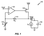
図1は、従来のLDO電圧調整器100を示す。図1に示すように、LDO電圧調整器100の差動増幅器102(「誤差増幅器」とも呼ばれる)は、入力基準電圧Vrefを受け入れ、調整済み出力電圧Vregを生成する。差動増幅器102の出力は、大型パストランジスタであるトランジスタ104(一態様では、pチャネル金属酸化物半導体(PMOS)であってもよい)を駆動する。LDO電圧調整器100は、負荷キャパシタ(C)106と抵抗器R1 108およびR2 110とをさらに含む。LDO電圧調整器100は、SoCの他のサブブロック用の負荷電流I0を供給する。負荷電流I0が負荷キャパシタ106に関連付けられていないことに留意されたい。負荷電流I0はシステムの残りの部分に供給され、負荷キャパシタ106は、LDO電圧調整器100が一定の低ノイズ出力電圧を供給できるように付加される。抵抗器R1 108およびR2 110はフィードバック回路を形成する。LDO電圧調整器100の出力電圧をプログラムするには一方の抵抗器を調整すれば十分である。
FIG. 1 shows a conventional
図1のLDO電圧調整器100などのLDO電圧調整器は「2極」システムである。「極」および「零」は電気回路の安定性を示す。より具体的には、システム(すなわち、LDO電圧調整器100)の極および零の周波数は、周波数に対してプロットされるループ利得およびループ位相を定義する。これらの極において回路の安定性を維持するために、各極は、ループ利得に対する減衰係数として働く他の回路素子によって補償される。たとえば抵抗器とキャパシタの複数の組合せがあるために複数の極が存在する場合、支配極の補償が着目されることがある。そのようなシステムでは、非支配極が支配極から離れて位置することが望ましい。この極配置は補償方法を介して実現されるべきである。
LDO voltage regulators, such as
図1を再び参照する。パスデバイス(たとえば、トランジスタ104)のゲートの所と負荷(たとえば、負荷キャパシタ106)の所に(比較的)低周波数の2つの極がある。LDO電圧調整器100は、安定性を確保するために、補償する必要がある。
Reference is again made to FIG. There are two (relatively) low frequency poles at the gate of the pass device (e.g., transistor 104) and the load (e.g., load capacitor 106). The
一例では、LDO電圧調整器100は、1.8Vなどの正電源電圧Vddによってバイアスされ、1.1Vの調整電圧を供給する高電力1.1VデジタルベースバンドLDOであってもよい。この例では、電流(I0)は5μA〜50mAの範囲で変化し、負荷キャパシタ106は、キャパシタンスが3.3μF〜約10μFの範囲である高負荷オフチップバイパスキャパシタである。10μFが安定性に関する極端な場合であることに留意されたい。大過渡電流を有する回路の場合、負荷調整を改善し電圧過渡を低減させるために大型オフチップバイパスキャパシタ(たとえば、負荷キャパシタ106)が使用される。
In one example,
オペアンプを補償して安定性とPSRRを同時に満たす課題は、バッテリー式デバイスおよび大型オフチップバイパスキャパシタ(たとえば、負荷キャパシタ106)などの超低電力用途向けの設計時には対処がより困難になる。従来、ミラー補償はオペアンプ安定化のロバストな方法であるが、上述の課題を考慮すると、ミラー補償では、チップ上に配置することができない大型補償キャパシタが必要である。ミラー補償では、電源電圧変動除去(PSR)も行われない。したがって、十分なPSRRも実現する入手可能なキャパシタを有する補償されたオペアンプが必要である。 The challenge of compensating op amps to simultaneously satisfy stability and PSRR becomes more difficult when designed for ultra-low power applications such as battery-powered devices and large off-chip bypass capacitors (eg, load capacitors 106). Conventionally, Miller compensation is a robust method of op amp stabilization, but given the above issues, Miller compensation requires a large compensation capacitor that can not be placed on chip. In Miller compensation, power supply voltage removal (PSR) is also not performed. Therefore, there is a need for a compensated op amp with an available capacitor that also achieves sufficient PSRR.
本開示は、LDO電圧調整器に補助増幅器を導入する。より具体的には、補助増幅器が補償キャパシタの前に付加される。補助増幅器によって与えられる利得に基づいて、補償キャパシタの効果が向上する。たとえば、補助増幅器が20dBの利得をもたらす場合、補償キャパシタの効果は10倍向上する。したがって、補償キャパシタを10倍小さくすることができる。たとえば、従来のミラー補償のための補償キャパシタが400ピコファラド(pF)である場合、補助増幅器を含む補償器用の補償キャパシタは40pF(すなわち、400pFの低減率が10倍であるときの値または400pFを10で割った値)であればよい。 The present disclosure introduces an auxiliary amplifier to the LDO voltage regulator. More specifically, an auxiliary amplifier is added in front of the compensation capacitor. Based on the gain provided by the auxiliary amplifier, the effect of the compensation capacitor is enhanced. For example, if the auxiliary amplifier provides a gain of 20 dB, the effect of the compensation capacitor is improved by a factor of ten. Therefore, the compensation capacitor can be reduced by 10 times. For example, if the compensation capacitor for conventional Miller compensation is 400 picofarads (pF), then the compensation capacitor for the compensator, including the auxiliary amplifier, is 40 pF (ie, the value when the 400 pF reduction factor is 10 or 400 pF). It should be a value divided by 10).
図2は、本開示の少なくとも1つの態様による補助増幅器214と補償キャパシタ212とを含むLDO電圧調整器200を示す。図1と同様に、LDO電圧調整器200の差動増幅器202は、入力基準電圧Vrefを受け入れ、調整済み出力電圧Vregを生成する。差動増幅器202の出力は、大型パストランジスタであるトランジスタ204(一態様では、PMOSであってもよい)を駆動する。LDO電圧調整器100と同様に、LDO電圧調整器200は、負荷キャパシタ(C)206と抵抗器R1 208およびR2 210とをさらに含む。LDO電圧調整器200は、システムの他のサブブロック用の負荷電流I0を供給する。しかし、LDO電圧調整器100とは異なり、LDO電圧調整器200は、前述のように補助増幅器214を補償キャパシタ212の前に含む。
FIG. 2 shows an
補償キャパシタ212の前に補助増幅器214を付加することの利点は、上記で説明したように補償キャパシタ212のサイズが補助増幅器214の利得の量だけ小さくなることを含む。たとえば、補助増幅器214が20dBの利得をもたらす場合、補償キャパシタ212の効果は10倍向上する。したがって、補償キャパシタ212は、LDO電圧調整器200が補助増幅器214のみを含む場合よりも10倍小さくすることができる。さらに、PSRRが補助増幅器214の利得の量だけ向上する。補助増幅器214がない場合、高周波数では、電源ノイズが直接LDO出力に結合し、電源電圧変動除去は生じない。
The advantages of adding the
一実施形態では、LDO電圧調整器(LDO電圧調整器100など)は短絡回路クランプを含むことができる。そのようなLDO電圧調整器は、バッテリーからの正電源電圧Vdd(たとえば、2V〜3.6V)を受け取り、1.8Vなどの調整済み出力電圧Vregを生成することができる。入力電圧が大きい場合、PMOSデバイス(たとえば、トランジスタ104)のゲートソース電圧が3.6Vにもなり、出力が短絡した場合にLDO電圧調整器において大きい電流を生成することがあるので、短絡回路保護手段を有することが好ましい。PMOSの出力を直列抵抗に付加すると、そのような短絡回路を制限することができるが、電圧ヘッドルームが低く、そのようなLDO電圧調整器が生成する電流が大きい場合、V=I*Rの電圧降下を回避することが好ましい。 In one embodiment, the LDO voltage regulator (eg, LDO voltage regulator 100) can include a short circuit clamp. Such LDO voltage regulator receives a positive supply voltage V dd from the battery (e.g., 2V~3.6V), it is possible to generate a regulated output voltage V reg, such as 1.8V. If the input voltage is large, the gate-source voltage of the PMOS device (for example, transistor 104) will be as high as 3.6V, which may generate a large current in the LDO voltage regulator if the output is shorted, so short circuit protection measures It is preferable to have Adding the output of the PMOS to the series resistor can limit such a short circuit, but with low voltage headroom and large currents generated by such LDO voltage regulators, V = I * R It is preferable to avoid voltage drops.
このような問題に対処するには、LDO電圧調整器にアクティブクランプを付加することができる。アクティブクランプは好ましくは、LDO電圧調整器の通常の動作には関与せず、その代わりにPMOSゲートを保持して電流の短絡回路サージを制限することを確実にする非線形であることが好ましい。 To address such issues, an active clamp can be added to the LDO voltage regulator. The active clamp is preferably not involved in the normal operation of the LDO voltage regulator, but instead is preferably non-linear to ensure that the PMOS gate is held to limit current short circuit surges.
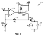
図3は、本開示の少なくとも1つの態様によるアクティブクランプ316を含むLDO電圧調整器300を示す。図1のLDO電圧調整器100と同様に、LDO電圧調整器300の差動増幅器302は、入力基準電圧Vrefを受け入れ、調整済み出力電圧を生成する。差動増幅器302の出力は、大型パストランジスタであるトランジスタ304(一態様では、PMOSであってもよい)を駆動する。LDO電圧調整器100と同様に、LDO電圧調整器300は、負荷キャパシタ(C)306と抵抗器R1 308およびR2 310とをさらに含む。LDO電圧調整器300は、システムの他のサブブロック用の負荷電流I0を供給する。
FIG. 3 shows an
図3に示すように、アクティブクランプ316は、差動増幅器302とトランジスタ304との間に配置される。LDO電圧調整器300内の(図7に示す)アクティブクランプ316の構成では、一般的なCMOS非線形性に対してアクティブクランプ316の非線形性が強調される。この構成では、オペアンプ利得を妨げないように出力抵抗が高く、出力抵抗を設計する際に自由度が得られる。LDO電圧調整器300は、たとえば2V〜3.6Vの、バッテリーからの正電源電圧Vddの供給を受け、たとえば1.8Vの調整済み出力電圧Vregをオフチップ負荷キャパシタに供給する。アクティブクランプ316がない場合、LDO電圧調整器300は、短絡回路保護手段を有さない。
As shown in FIG. 3, an
図4は、本開示の少なくとも1つの態様による補助増幅器414と、補償キャパシタ412と、アクティブクランプ416とを含むLDO電圧調整器400を示す。図2と同様に、LDO電圧調整器400の差動増幅器402は、入力基準電圧Vrefを受け入れ、調整済み出力電圧を生成する。差動増幅器402の出力は、大型パストランジスタであるトランジスタ404(一態様では、PMOSデバイスであってもよい)を駆動する。LDO電圧調整器400はさらに、前述のように、負荷キャパシタ(C)406と、抵抗器R1 408およびR2 410と、補助増幅器414とを補償キャパシタ412の前に含む。
FIG. 4 illustrates an
図4の例では、LDO電圧調整器400は、図3を参照しながら上記で説明したように、差動増幅器402とトランジスタ404との間に配置されたアクティブクランプ416も含む。LDO電圧調整器300と同様に、LDO電圧調整器400は、たとえば2V〜3.6Vの、バッテリーからの正電源電圧Vddの供給を受け、たとえば1.8Vの調整済み出力電圧をオフチップ負荷キャパシタに供給する。
In the example of FIG. 4, the
図5は、本開示の少なくとも1つの態様による図2の差動増幅器202、図3の差動増幅器302、または図4の差動増幅器402などの差動増幅器502の図である。差動増幅器502は、1.2マイクロアンペア(μA)などの低バイアス電流Ibiasを使用する。その理由は、上述のように、低バイアス電流Ibiasが低電力バッテリー式デバイスにおいて利用される(たとえば、差動増幅器502の正電源電圧Vddは1.3Vであってもよい)からである。差動増幅器502は、たとえば、DC800mVの電圧、およびたとえば、バンドギャップ電流Ibandgapによって与えられる25ナノアンペア(nA)の電流によってバイアスされる。
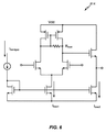
5 is a diagram of a
図6は、本開示の少なくとも1つの態様による、図2の補助増幅器214、図3の補助増幅器314、および図4の補助増幅器414などの補助増幅器614の図である。補助増幅器614は、利得を制限するための、5MΩなどの抵抗性負荷Rloadを有する低電力開ループ差動増幅器である。一例では、正電源電圧Vddは1.3Vであってもよく、バンドギャップ電流Ibandgapは25nAであってもよく、第1のバイアス電流Ibias1は650nAであってもよく、第2のバイアス電流Ibias2は1.4μAであってもよい。
6 is a diagram of an
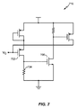
図7は、本開示の少なくとも1つの態様による図3のアクティブクランプ316および/または図4のアクティブクランプ416などのアクティブクランプ716の図である。LDO電圧調整器(たとえば、図3のLDO電圧調整器300または図4のLDO電圧調整器400)の出力が短絡されると、アクティブクランプ716がない場合、制御電圧VCとも呼ばれるパスデバイス(たとえば、図3のトランジスタ304または図4のトランジスタ404)のゲート電圧が過度に降下し(たとえば、100mVよりも低くなり)、パスデバイスを電流の顕著なサージ(たとえば、2アンペア程度)が通過する。しかし、アクティブクランプ716がある場合、VCの電圧降下によってデバイス702に電流の流れが生じる。この電流は、抵抗器704を通過し、次いで別のデバイス706によって増幅されVCに対する非線形性が強調される。VCの降下が小さい(たとえば、0.5V)場合、電流がノードVCに流入する。アクティブクランプ716がない場合、VCは0Vまで降下することがある。流入した電流は差動増幅器(たとえば、図3の差動増幅器302または図4の差動増幅器402)によって引き込まれ、差動増幅器の制限されたバイアス電流によってアクティブクランプ716内の電流が制限される。その結果、VCが過度に降下することはできなくなる。たとえば、LDO電圧調整器における3.6Vバッテリー電圧では、VCの2V降下は過度であり、一方、VCの0.5V降下は許容される。電流のサージに関しては、2Aの電流は過度であり、一方、200mAの電流は許容される。
7 is an illustration of an
図8は、本開示の少なくとも1つの態様によるLDO電圧調整器を補償するための例示的なフロー800を示す。LDO電圧調整器は閉ループ演算増幅器であってもよい。一態様では、LDO電圧調整器はミラー補償を利用してもよい。
FIG. 8 shows an
フロー800は、802において、基準電圧と調整済み出力電圧との差分を差動増幅器(たとえば、図2の差動増幅器202、図3の差動増幅器302、または図4の差動増幅器402)によって増幅することを含む。
フロー800は、804において、差動増幅器の出力を差動増幅器に結合されたパストランジスタ(たとえば、図2のトランジスタ204、図3のトランジスタ304、または図4のトランジスタ404)において受け取ることを含む。
フロー800は、806において、補助増幅器(たとえば、図2の補助増幅器214または図4の補助増幅器414)からの出力信号を補償キャパシタ(たとえば、図2の補償キャパシタ212または図4の補償キャパシタ412)において受け取ることを含む。図2および図4に示すように、補償キャパシタは、差動増幅器の出力ノードに結合されてもよく、補助増幅器の出力ノードは補償キャパシタに結合されてもよく、補助増幅器の入力ノードはパストランジスタに結合されてもよい。補助増幅器は、低電流開ループ差動増幅器であってもよい。たとえば、低電流は25ナノアンペアの電流であってもよい。
フロー800は、808において、場合によっては、差動増幅器の出力ノードおよびパストランジスタにアクティブクランプを結合することを含む。アクティブクランプは、パストランジスタからの短絡回路電流サージを制限する。パストランジスタは、バッテリーからの2V〜3.6Vの電圧を受け取り、LDO電圧調整器はオフチップ負荷キャパシタに1.8Vの電圧を供給する。
一態様では、補助増幅器からの出力信号が、補助増幅器からの入力信号によって与えられる利得の量に基づいて補償キャパシタの補償を増強させてもよい。その場合、補償キャパシタの補償がLDO電圧調整器を含む回路を安定化させる。 In one aspect, the output signal from the auxiliary amplifier may enhance the compensation of the compensation capacitor based on the amount of gain provided by the input signal from the auxiliary amplifier. In that case, compensation of the compensation capacitor stabilizes the circuit including the LDO voltage regulator.
別の態様では、補助増幅器によって与えられる利得の量に基づいてLDO電圧調整器を含む回路のPSRRが向上する場合がある。 In another aspect, the PSRR of a circuit including an LDO voltage regulator may be improved based on the amount of gain provided by the auxiliary amplifier.
また別の態様では、補助増幅器は、補助増幅器の利得の量を制限する抵抗性負荷を含んでもよい。 In yet another aspect, the auxiliary amplifier may include a resistive load that limits the amount of gain of the auxiliary amplifier.
当業者には、情報および信号が、様々な異なる技術および技法のいずれかを使用して表されてよいことが諒解されよう。たとえば、上記の説明全体にわたって言及されることがあるデータ、命令、コマンド、情報、信号、ビット、シンボル、およびチップは、電圧、電流、電磁波、磁場もしくは磁性粒子、光場もしくは光学粒子、またはそれらの任意の組合せによって表されてもよい。 Those skilled in the art will appreciate that information and signals may be represented using any of a variety of different technologies and techniques. For example, data, instructions, commands, information, signals, bits, symbols and chips that may be mentioned throughout the above description may be voltage, current, electromagnetic waves, magnetic fields or particles, light fields or particles, or they May be represented by any combination of
さらに、本明細書で開示する実施形態に関して説明する様々な例証的な論理ブロック、モジュール、回路、およびアルゴリズムステップが、電子ハードウェア、コンピュータソフトウェア、または両方の組合せとして実装されてもよいことが、当業者には諒解されよう。ハードウェアとソフトウェアのこの互換性を明確に示すために、上記では、様々な例証的な構成要素、ブロック、モジュール、回路、およびステップについて、全般的にそれらの機能の観点から説明した。そのような機能が、ハードウェアとして実現されるか、ソフトウェアとして実現されるかは、特定の適用例と、システム全体に課される設計制約とによって決まる。当業者は説明した機能を特定の適用例ごとに様々な方法で実装してもよいが、そのような実装決定は、本開示の範囲からの逸脱を引き起こすものと解釈されるべきでない。 Additionally, various illustrative logic blocks, modules, circuits, and algorithmic steps described in connection with the embodiments disclosed herein may be implemented as electronic hardware, computer software, or a combination of both. Those skilled in the art will appreciate. To clearly illustrate this interchangeability of hardware and software, various illustrative components, blocks, modules, circuits, and steps have been described above generally in terms of their functionality. Whether such functionality is implemented as hardware or software depends upon the particular application and design constraints imposed on the overall system. Skilled artisans may implement the described functionality in varying ways for each particular application, but such implementation decisions should not be interpreted as causing a departure from the scope of the present disclosure.
本明細書で開示する実施形態に関して説明する様々な例示的な論理ブロック、モジュール、および回路は、汎用プロセッサ、デジタルシグナルプロセッサ(DSP)、特定用途用集積回路(ASIC)、フィールドプログラマブルゲートアレイ(FPGA)もしくは他のプログラマブル論理デバイス、個別のゲートもしくはトランジスタ論理、個別のハードウェア構成要素、または本明細書で説明した機能を果たすように設計されたこれらの任意の組合せを用いて実装されるか、または実行される場合がある。汎用プロセッサはマイクロプロセッサであってもよいが、代替として、プロセッサは任意の従来のプロセッサ、コントローラ、マイクロコントローラ、またはステートマシンであってもよい。プロセッサはまた、コンピューティングデバイスの組合せ、たとえば、DSPとマイクロプロセッサとの組合せ、複数のマイクロプロセッサ、DSPコアと連携した1つもしくは複数のマイクロプロセッサ、または任意の他のそのような構成として実装してもよい。 Various exemplary logic blocks, modules, and circuits described with respect to the embodiments disclosed herein may be implemented as general purpose processors, digital signal processors (DSPs), application specific integrated circuits (ASICs), field programmable gate arrays (FPGAs) Or other programmable logic devices, discrete gate or transistor logic, discrete hardware components, or any combination thereof designed to perform the functions described herein, or Or may be executed. A general purpose processor may be a microprocessor, but in the alternative, the processor may be any conventional processor, controller, microcontroller, or state machine. The processor may also be implemented as a combination of computing devices, eg, a combination of a DSP and a microprocessor, a plurality of microprocessors, one or more microprocessors in conjunction with a DSP core, or any other such configuration. May be
本明細書において開示される実施形態に関して説明した方法、シーケンス、および/またはアルゴリズムは、ハードウェアにおいて直接具現化される場合も、プロセッサによって実行されるソフトウェアモジュールにおいて具現化される場合も、あるいは2つの組合せにおいて具現化される場合もある。ソフトウェアモジュールは、RAMメモリ、フラッシュメモリ、ROMメモリ、EPROMメモリ、EEPROMメモリ、レジスタ、ハードディスク、リムーバブルディスク、CD-ROM、または当技術分野において知られている任意の他の形の記憶媒体内に存在してもよい。例示的な記憶媒体は、プロセッサが記憶媒体から情報を読み取り、記憶媒体に情報を書き込むことができるようにプロセッサに結合される。代替として、記憶媒体は、プロセッサと一体化してもよい。プロセッサおよび記憶媒体は、ASICの中に存在する場合がある。ASICはユーザ端末(たとえば、UE)内に存在してもよい。代替として、プロセッサおよび記憶媒体は、個別構成要素としてユーザ端末内に存在する場合がある。 The methods, sequences, and / or algorithms described in connection with the embodiments disclosed herein may be embodied directly in hardware or in software modules executed by a processor, or 2 It may be embodied in one combination. The software module resides in RAM memory, flash memory, ROM memory, EPROM memory, EEPROM memory, registers, hard disk, removable disk, CD-ROM, or any other form of storage medium known in the art You may An exemplary storage medium is coupled to the processor such that the processor can read information from, and write information to, the storage medium. In the alternative, the storage medium may be integral to the processor. The processor and the storage medium may reside in an ASIC. The ASIC may reside in a user terminal (eg, a UE). In the alternative, the processor and the storage medium may reside as discrete components in a user terminal.
1つまたは複数の例示的な実施形態では、説明する機能は、ハードウェア、ソフトウェア、ファームウェア、またはそれらの任意の組合せにおいて実装されてもよい。ソフトウェアで実装される場合、機能は、1つもしくは複数の命令またはコードとして、コンピュータ可読媒体上に記憶されてもよく、またはコンピュータ可読媒体を介して送信されてもよい。コンピュータ可読媒体は、コンピュータ記憶媒体と、ある場所から別の場所へのコンピュータプログラムの伝達を容易にする任意の媒体を含む通信媒体の両方を含む。記憶媒体は、コンピュータによってアクセスされることがある任意の利用可能な媒体であってもよい。限定ではなく例として、そのようなコンピュータ可読媒体は、RAM、ROM、EEPROM、CD-ROMまたは他の光ディスクストレージ、磁気ディスクストレージまたは他の磁気記憶デバイス、あるいは命令またはデータ構造の形態で所望のプログラムコードを搬送または記憶するために使用できるとともにコンピュータによってアクセスできる任意の他の媒体を含むことができる。また、いかなる接続も、厳密にはコンピュータ可読媒体と呼ばれる。たとえば、ソフトウェアが、同軸ケーブル、光ファイバーケーブル、ツイストペア、デジタル加入者回線(DSL)、または赤外線、無線、およびマイクロ波などのワイヤレス技術を使用してウェブサイト、サーバ、または他のリモートソースから送信される場合、同軸ケーブル、光ファイバーケーブル、ツイストペア、DSL、または赤外線、無線、およびマイクロ波などのワイヤレス技術は、媒体の定義に含まれる。本明細書で使用するディスク(disk)およびディスク(disc)は、コンパクトディスク(disc)(CD)、レーザーディスク(登録商標)(disc)、光ディスク(disc)、デジタル多用途ディスク(disc)(DVD)、フロッピー(登録商標)ディスク(disk)、およびBlu-ray(登録商標)ディスク(disc)を含み、ディスク(disk)は通常、データを磁気的に再生し、ディスク(disc)は、レーザーを用いてデータを光学的に再生する。上記の組合せもまた、コンピュータ可読媒体の範囲内に含まれるべきである。 In one or more exemplary embodiments, the functions described may be implemented in hardware, software, firmware, or any combination thereof. If implemented in software, the functions may be stored on or read out of computer readable media as one or more instructions or code. Computer-readable media includes both computer storage media and communication media including any medium that facilitates transfer of a computer program from one place to another. A storage media may be any available media that may be accessed by a computer. By way of example and not limitation, such computer readable media may be RAM, ROM, EEPROM, CD-ROM or other optical disk storage, magnetic disk storage or other magnetic storage device, or any desired program in the form of instructions or data structures. It may include any other medium that can be used to carry or store code and that can be accessed by a computer. Also, any connection is properly termed a computer-readable medium. For example, software may be transmitted from a website, server, or other remote source using coaxial technology, fiber optic cable, twisted pair, digital subscriber line (DSL), or wireless technologies such as infrared, wireless, and microwave. In that case, wireless technology such as coaxial cable, fiber optic cable, twisted pair, DSL, or infrared, wireless, and microwave are included in the definition of medium. As used herein, discs and discs are compact discs (CDs), laser discs (registered trademark) (discs), optical discs (discs), digital versatile discs (disc) (DVDs) Disk) and a Blu-ray® disc, the disc normally regenerating data magnetically, the disc comprising a laser. Use to optically reproduce data. Combinations of the above should also be included within the scope of computer readable media.
上記の開示は本開示の例示的な実施形態を示すが、添付の特許請求の範囲によって規定される本開示の範囲から逸脱することなく、本明細書において様々な変更および修正が行われ得ることに留意されたい。本明細書で説明した本開示の実施形態による方法クレームの機能、ステップおよび/またはアクションは、特定の順序で実行される必要はない。さらに、本開示の要素は、単数形において説明または特許請求がなされる場合があるが、単数形に限定することが明示的に述べられていない限り、複数形が企図される。 While the above disclosure represents exemplary embodiments of the present disclosure, various changes and modifications may be made herein without departing from the scope of the present disclosure as defined by the appended claims. Please note. The functions, steps and / or actions of the method claims in accordance with the embodiments of the present disclosure described herein need not be performed in any particular order. Furthermore, although elements of the present disclosure may be described or claimed in the singular, the plural is contemplated unless limitation to the singular is explicitly stated.
100 従来のLDO電圧調整器
102 差動増幅器
104 トランジスタ
106 負荷キャパシタ
108 抵抗器R1
110 抵抗器R2
200 LDO電圧調整器
202 差動増幅器
204 トランジスタ
206 負荷キャパシタ
208 抵抗器R1
210 抵抗器R2
212 補償キャパシタ
214 補助増幅器
300 LDO電圧調整器
302 差動増幅器
304 トランジスタ
306 負荷キャパシタ
308 抵抗器R1
310 抵抗器R2
316 アクティブクランプ
400 LDO電圧調整器
402 差動増幅器
404 トランジスタ
406 負荷キャパシタ
408 抵抗器R1
410 抵抗器R2
412 補償キャパシタ
414 補助増幅器
416 アクティブクランプ
502 差動増幅器
614 補助増幅器
702 デバイス
704 抵抗器
706 別のデバイス
716 アクティブクランプ
I0 負荷電流
Vdd 正電源電圧
Vreg 調整済み出力電圧
100 Traditional LDO Voltage Regulators
102 differential amplifier
104 transistor
106 load capacitor
108 Resistor R 1
110 Resistor R 2
200 LDO Voltage Regulator
202 differential amplifier
204 transistor
206 Load capacitor
208 resistor R 1
210 Resistor R 2
212 compensation capacitor
214 auxiliary amplifier
300 LDO Voltage Regulator
302 differential amplifier
304 transistor
306 Load capacitor
308 Resistor R 1
310 Resistor R 2
316 Active clamp
400 LDO Voltage Regulator
402 differential amplifier
404 transistor
406 Load capacitor
408 Resistor R 1
410 Resistor R 2
412 Compensation capacitor
414 auxiliary amplifier
416 Active clamp
502 differential amplifier
614 Auxiliary amplifier
702 device
704 resistor
706 Another device
716 Active clamp
I 0 load current
V dd positive power supply voltage
V reg adjusted output voltage
Claims (30)
基準電圧と調整済み出力電圧との差分を増幅するように構成された差動増幅器と、
前記差動増幅器に結合され、前記差動増幅器の出力によって駆動されるパストランジスタと、
前記差動増幅器の出力ノードに結合された補償キャパシタと、
補助増幅器であって、前記補助増幅器の出力ノードが前記補償キャパシタに結合され、前記補助増幅器の入力ノードが前記パストランジスタに結合される補助増幅器とを備えるLDO電圧調整器。 Low dropout (LDO) voltage regulator,
A differential amplifier configured to amplify the difference between the reference voltage and the regulated output voltage;
A pass transistor coupled to the differential amplifier and driven by the output of the differential amplifier;
A compensation capacitor coupled to the output node of the differential amplifier;
An auxiliary amplifier, comprising: an auxiliary amplifier output node coupled to the compensation capacitor; and an auxiliary amplifier input node coupled to the pass transistor.
基準電圧と調整済み出力電圧との差分を差動増幅器によって増幅するステップと、
前記差動増幅器に結合されたパストランジスタにおいて、前記差動増幅器の出力を受け取るステップと、
補償キャパシタにおいて補助増幅器からの出力信号を受け取るステップであって、前記補償キャパシタが、前記差動増幅器の出力ノードに結合され、前記補助増幅器の出力ノードが、前記補償キャパシタに結合され、前記補助増幅器の入力ノードが、前記パストランジスタに結合される、ステップとを含む方法。 A method for compensating a low dropout (LDO) voltage regulator, comprising:
Amplifying the difference between the reference voltage and the regulated output voltage by a differential amplifier;
Receiving an output of the differential amplifier at a pass transistor coupled to the differential amplifier;
Receiving an output signal from an auxiliary amplifier at a compensation capacitor, the compensation capacitor being coupled to an output node of the differential amplifier, an output node of the auxiliary amplifier being coupled to the compensation capacitor, the auxiliary amplifier And the input node of is coupled to the pass transistor.
基準電圧と調整済み出力電圧との差分を増幅するように構成された差動増幅器と、
前記差動増幅器に結合され、前記差動増幅器の出力によって駆動されるパストランジスタと、
前記差動増幅器の出力ノードに結合された補償手段と、
補助増幅手段であって、前記補助増幅手段の出力ノードが前記補償手段に結合され、前記補助増幅手段の入力ノードが前記パストランジスタに結合される補助増幅手段とを備える装置。 A device for compensating low dropout (LDO) voltage regulators, comprising:
A differential amplifier configured to amplify the difference between the reference voltage and the regulated output voltage;
A pass transistor coupled to the differential amplifier and driven by the output of the differential amplifier;
Compensation means coupled to the output node of the differential amplifier;
Auxiliary amplifying means, comprising: auxiliary amplifying means, wherein an output node of the auxiliary amplifying means is coupled to the compensating means, and an input node of the auxiliary amplifying means is coupled to the pass transistor.
基準電圧と調整済み出力電圧との差分を差動増幅器によって増幅するための少なくとも1つの命令と、
前記差動増幅器に結合されたパストランジスタにおいて、前記差動増幅器の出力を受け取るための少なくとも1つの命令と、
補償キャパシタにおいて補助増幅器からの出力信号を受け取るための少なくとも1つの命令であって、前記補償キャパシタが、前記差動増幅器の出力ノードに結合され、前記補助増幅器の出力ノードが、前記補償キャパシタに結合され、前記補助増幅器の入力ノードが、前記パストランジスタに結合される少なくとも1つの命令とを含む非一時的コンピュータ可読記憶媒体。 A non-transitory computer readable storage medium for compensating a low dropout (LDO) voltage regulator, comprising:
At least one instruction for amplifying the difference between the reference voltage and the regulated output voltage by the differential amplifier;
At least one instruction for receiving the output of the differential amplifier in a pass transistor coupled to the differential amplifier;
At least one instruction for receiving an output signal from an auxiliary amplifier at a compensation capacitor, wherein the compensation capacitor is coupled to an output node of the differential amplifier, and an output node of the auxiliary amplifier is coupled to the compensation capacitor Non-transitory computer readable storage medium, wherein the input node of the auxiliary amplifier comprises at least one instruction coupled to the pass transistor.
Applications Claiming Priority (3)
| Application Number | Priority Date | Filing Date | Title |
|---|---|---|---|
| US15/186,411 US10175706B2 (en) | 2016-06-17 | 2016-06-17 | Compensated low dropout with high power supply rejection ratio and short circuit protection |
| US15/186,411 | 2016-06-17 | ||
| PCT/US2017/033812 WO2017218141A1 (en) | 2016-06-17 | 2017-05-22 | Compensated low dropout with high power supply rejection ratio and short circuit protection |
Publications (2)
| Publication Number | Publication Date |
|---|---|
| JP2019518282A true JP2019518282A (en) | 2019-06-27 |
| JP2019518282A5 JP2019518282A5 (en) | 2020-06-18 |
Family
ID=58794252
Family Applications (1)
| Application Number | Title | Priority Date | Filing Date |
|---|---|---|---|
| JP2018560981A Pending JP2019518282A (en) | 2016-06-17 | 2017-05-22 | Low dropout compensation with high supply rejection and short circuit protection |
Country Status (7)
| Country | Link |
|---|---|
| US (1) | US10175706B2 (en) |
| EP (1) | EP3472682A1 (en) |
| JP (1) | JP2019518282A (en) |
| KR (1) | KR20190018424A (en) |
| CN (1) | CN109219786A (en) |
| BR (1) | BR112018075103A2 (en) |
| WO (1) | WO2017218141A1 (en) |
Cited By (1)
| Publication number | Priority date | Publication date | Assignee | Title |
|---|---|---|---|---|
| JP7469573B2 (en) | 2021-03-25 | 2024-04-16 | クアルコム,インコーポレイテッド | Enhanced power supply rejection |
Families Citing this family (17)
| Publication number | Priority date | Publication date | Assignee | Title |
|---|---|---|---|---|
| US9817416B2 (en) * | 2015-08-17 | 2017-11-14 | Skyworks Solutions, Inc. | Apparatus and methods for programmable low dropout regulators for radio frequency electronics |
| US20190087700A1 (en) * | 2016-02-29 | 2019-03-21 | Gerd Reime | Bidirectional transponder with low energy use |
| CN106708153B (en) * | 2017-03-08 | 2019-03-12 | 长江存储科技有限责任公司 | A kind of high bandwidth low pressure difference linear voltage regulator |
| JP6755399B2 (en) * | 2017-07-03 | 2020-09-16 | 三菱電機株式会社 | Short circuit protection circuit for semiconductor switching elements |
| US10382030B2 (en) * | 2017-07-12 | 2019-08-13 | Texas Instruments Incorporated | Apparatus having process, voltage and temperature-independent line transient management |
| US11009901B2 (en) * | 2017-11-15 | 2021-05-18 | Qualcomm Incorporated | Methods and apparatus for voltage regulation using output sense current |
| US10411599B1 (en) | 2018-03-28 | 2019-09-10 | Qualcomm Incorporated | Boost and LDO hybrid converter with dual-loop control |
| US10444780B1 (en) | 2018-09-20 | 2019-10-15 | Qualcomm Incorporated | Regulation/bypass automation for LDO with multiple supply voltages |
| US10591938B1 (en) | 2018-10-16 | 2020-03-17 | Qualcomm Incorporated | PMOS-output LDO with full spectrum PSR |
| US10545523B1 (en) | 2018-10-25 | 2020-01-28 | Qualcomm Incorporated | Adaptive gate-biased field effect transistor for low-dropout regulator |
| US10726881B1 (en) * | 2019-04-08 | 2020-07-28 | Texas Instruments Incorporated | Supply voltage clamping for improved power supply rejection ratio |
| US11372436B2 (en) | 2019-10-14 | 2022-06-28 | Qualcomm Incorporated | Simultaneous low quiescent current and high performance LDO using single input stage and multiple output stages |
| US11526187B2 (en) * | 2020-01-03 | 2022-12-13 | Skyworks Solutions, Inc. | Method and system for boosting output current |
| DE102020115851B3 (en) | 2020-06-16 | 2021-10-28 | Infineon Technologies Ag | FAST VOLTAGE REGULATOR AND METHOD OF VOLTAGE REGULATION |
| CN112130612A (en) * | 2020-09-23 | 2020-12-25 | 中国电子科技集团公司第五十八研究所 | Large-current linear voltage regulator circuit with stability compensation |
| CN114442714A (en) * | 2020-11-02 | 2022-05-06 | 圣邦微电子(北京)股份有限公司 | Novel clamp structure for Vgs of clamp PMOS |
| CN112327987B (en) * | 2020-11-18 | 2022-03-29 | 上海艾为电子技术股份有限公司 | Low dropout regulator and electronic equipment |
Citations (5)
| Publication number | Priority date | Publication date | Assignee | Title |
|---|---|---|---|---|
| JP2002343874A (en) * | 2001-05-17 | 2002-11-29 | Nippon Telegr & Teleph Corp <Ntt> | Series regulator circuit |
| JP2005202781A (en) * | 2004-01-16 | 2005-07-28 | Artlogic Inc | Voltage regulator |
| JP2007048283A (en) * | 2005-08-05 | 2007-02-22 | Micrel Inc | Zero cancellation in multiloop voltage regulator control scheme |
| JP2007157071A (en) * | 2005-12-08 | 2007-06-21 | Rohm Co Ltd | Regulator circuit, and automobile mounted therewith |
| JP2013527527A (en) * | 2010-04-29 | 2013-06-27 | クアルコム,インコーポレイテッド | On-chip low voltage capacitorless low dropout regulator with adjustable Q factor |
Family Cites Families (17)
| Publication number | Priority date | Publication date | Assignee | Title |
|---|---|---|---|---|
| GB2356991B (en) | 1999-12-02 | 2003-10-22 | Zetex Plc | A negative feedback amplifier circuit |
| US6246221B1 (en) * | 2000-09-20 | 2001-06-12 | Texas Instruments Incorporated | PMOS low drop-out voltage regulator using non-inverting variable gain stage |
| US6522112B1 (en) | 2001-11-08 | 2003-02-18 | National Semiconductor Corporation | Linear regulator compensation inversion |
| US6600299B2 (en) | 2001-12-19 | 2003-07-29 | Texas Instruments Incorporated | Miller compensated NMOS low drop-out voltage regulator using variable gain stage |
| DE60225124T2 (en) * | 2002-07-05 | 2009-02-19 | Dialog Semiconductor Gmbh | Control device with low loss voltage, with a large load range and fast inner control loop |
| US6977490B1 (en) * | 2002-12-23 | 2005-12-20 | Marvell International Ltd. | Compensation for low drop out voltage regulator |
| US7002409B1 (en) | 2004-02-11 | 2006-02-21 | Marvell International Ltd. | Compensation circuit for amplifiers having multiple stages |
| US6975099B2 (en) * | 2004-02-27 | 2005-12-13 | Texas Instruments Incorporated | Efficient frequency compensation for linear voltage regulators |
| KR100608112B1 (en) | 2004-08-27 | 2006-08-02 | 삼성전자주식회사 | Power regulator having over-current protection circuit and method of over-current protection thereof |
| US7446515B2 (en) | 2006-08-31 | 2008-11-04 | Texas Instruments Incorporated | Compensating NMOS LDO regulator using auxiliary amplifier |
| TWI332134B (en) * | 2006-12-28 | 2010-10-21 | Ind Tech Res Inst | Adaptive pole and zero & pole zero cancellation control low drop-out voltage regulator |
| US7710091B2 (en) * | 2007-06-27 | 2010-05-04 | Sitronix Technology Corp. | Low dropout linear voltage regulator with an active resistance for frequency compensation to improve stability |
| CN201152948Y (en) * | 2008-02-03 | 2008-11-19 | 深圳艾科创新微电子有限公司 | Variable outputting linear voltage regulator having short circuit protection |
| US9134743B2 (en) * | 2012-04-30 | 2015-09-15 | Infineon Technologies Austria Ag | Low-dropout voltage regulator |
| CN102722207B (en) * | 2012-05-28 | 2014-08-20 | 华为技术有限公司 | Low dropout regulator (LDO) |
| EP2816438B1 (en) | 2013-06-20 | 2017-11-15 | Dialog Semiconductor GmbH | Active clamps for multi-stage amplifiers in over/under-voltage condition |
| US9552004B1 (en) * | 2015-07-26 | 2017-01-24 | Freescale Semiconductor, Inc. | Linear voltage regulator |
-
2016
- 2016-06-17 US US15/186,411 patent/US10175706B2/en active Active
-
2017
- 2017-05-22 EP EP17726511.3A patent/EP3472682A1/en not_active Withdrawn
- 2017-05-22 KR KR1020187035273A patent/KR20190018424A/en not_active Application Discontinuation
- 2017-05-22 WO PCT/US2017/033812 patent/WO2017218141A1/en unknown
- 2017-05-22 CN CN201780034598.8A patent/CN109219786A/en active Pending
- 2017-05-22 BR BR112018075103A patent/BR112018075103A2/en not_active IP Right Cessation
- 2017-05-22 JP JP2018560981A patent/JP2019518282A/en active Pending
Patent Citations (5)
| Publication number | Priority date | Publication date | Assignee | Title |
|---|---|---|---|---|
| JP2002343874A (en) * | 2001-05-17 | 2002-11-29 | Nippon Telegr & Teleph Corp <Ntt> | Series regulator circuit |
| JP2005202781A (en) * | 2004-01-16 | 2005-07-28 | Artlogic Inc | Voltage regulator |
| JP2007048283A (en) * | 2005-08-05 | 2007-02-22 | Micrel Inc | Zero cancellation in multiloop voltage regulator control scheme |
| JP2007157071A (en) * | 2005-12-08 | 2007-06-21 | Rohm Co Ltd | Regulator circuit, and automobile mounted therewith |
| JP2013527527A (en) * | 2010-04-29 | 2013-06-27 | クアルコム,インコーポレイテッド | On-chip low voltage capacitorless low dropout regulator with adjustable Q factor |
Cited By (1)
| Publication number | Priority date | Publication date | Assignee | Title |
|---|---|---|---|---|
| JP7469573B2 (en) | 2021-03-25 | 2024-04-16 | クアルコム,インコーポレイテッド | Enhanced power supply rejection |
Also Published As
| Publication number | Publication date |
|---|---|
| US10175706B2 (en) | 2019-01-08 |
| BR112018075103A2 (en) | 2019-03-26 |
| CN109219786A (en) | 2019-01-15 |
| US20170364110A1 (en) | 2017-12-21 |
| EP3472682A1 (en) | 2019-04-24 |
| KR20190018424A (en) | 2019-02-22 |
| WO2017218141A1 (en) | 2017-12-21 |
Similar Documents
| Publication | Publication Date | Title |
|---|---|---|
| US10175706B2 (en) | Compensated low dropout with high power supply rejection ratio and short circuit protection | |
| US10534385B2 (en) | Voltage regulator with fast transient response | |
| US8872492B2 (en) | On-chip low voltage capacitor-less low dropout regulator with Q-control | |
| US8154263B1 (en) | Constant GM circuits and methods for regulating voltage | |
| US9553548B2 (en) | Low drop out voltage regulator and method therefor | |
| CN208848104U (en) | A kind of low pressure difference linear voltage regulator of fast transient response | |
| US10873257B2 (en) | Low dropout regulator with smart offset | |
| CN114253330A (en) | Quick transient response's no off-chip capacitance low dropout linear voltage regulator | |
| TW201933022A (en) | Voltage regulator apparatus | |
| CN113467559B (en) | Adaptive dynamic zero compensation circuit applied to LDO (low dropout regulator) | |
| CN110618724A (en) | Voltage regulation system and method | |
| US20170293313A1 (en) | Low dropout regulator with pmos power transistor | |
| GB2539457A (en) | Voltage regulators | |
| WO2022082656A1 (en) | Low dropout linear regulator and power supply circuit | |
| CN107305399B (en) | PMOS power electric crystal linear voltage decreasing regulator circuits | |
| TW201821925A (en) | Voltage regulator | |
| US20140035545A1 (en) | High unity gain bandwidth voltage regulation for integrated circuits | |
| CN110366713A (en) | For compensating the method and circuit system of low pressure difference linear voltage regulator | |
| GB2557224A (en) | Voltage regulator | |
| CN110692196A (en) | Differential amplifier based on inverter | |
| TW201709004A (en) | Flipped voltage zero compensation circuit | |
| JP5859644B2 (en) | Amplifier with high power supply noise rejection | |
| Zhou et al. | A Fast-Transient Response Capacitor-Less FVF-LDO in 22-nm CMOS Technology | |
| JP2020013198A (en) | Voltage regulator and control method of voltage regulator | |
| Peng et al. | A high current efficiency rail-to-rail buffer for low drop-out regulators with load regulation-enhanced |
Legal Events
| Date | Code | Title | Description |
|---|---|---|---|
| A521 | Request for written amendment filed |
Free format text: JAPANESE INTERMEDIATE CODE: A523 Effective date: 20200427 |
|
| A621 | Written request for application examination |
Free format text: JAPANESE INTERMEDIATE CODE: A621 Effective date: 20200427 |
|
| A131 | Notification of reasons for refusal |
Free format text: JAPANESE INTERMEDIATE CODE: A131 Effective date: 20210222 |
|
| A02 | Decision of refusal |
Free format text: JAPANESE INTERMEDIATE CODE: A02 Effective date: 20210927 |