JP2019511168A - Variable frequency RC oscillator - Google Patents
Variable frequency RC oscillator Download PDFInfo
- Publication number
- JP2019511168A JP2019511168A JP2018545918A JP2018545918A JP2019511168A JP 2019511168 A JP2019511168 A JP 2019511168A JP 2018545918 A JP2018545918 A JP 2018545918A JP 2018545918 A JP2018545918 A JP 2018545918A JP 2019511168 A JP2019511168 A JP 2019511168A
- Authority
- JP
- Japan
- Prior art keywords
- delay
- circuit
- delay section
- variable
- network
- Prior art date
- Legal status (The legal status is an assumption and is not a legal conclusion. Google has not performed a legal analysis and makes no representation as to the accuracy of the status listed.)
- Pending
Links
Images


Classifications
-
- H—ELECTRICITY
- H03—ELECTRONIC CIRCUITRY
- H03K—PULSE TECHNIQUE
- H03K3/00—Circuits for generating electric pulses; Monostable, bistable or multistable circuits
- H03K3/02—Generators characterised by the type of circuit or by the means used for producing pulses
- H03K3/027—Generators characterised by the type of circuit or by the means used for producing pulses by the use of logic circuits, with internal or external positive feedback
- H03K3/03—Astable circuits
- H03K3/0315—Ring oscillators
-
- H—ELECTRICITY
- H03—ELECTRONIC CIRCUITRY
- H03K—PULSE TECHNIQUE
- H03K3/00—Circuits for generating electric pulses; Monostable, bistable or multistable circuits
- H03K3/02—Generators characterised by the type of circuit or by the means used for producing pulses
- H03K3/027—Generators characterised by the type of circuit or by the means used for producing pulses by the use of logic circuits, with internal or external positive feedback
- H03K3/03—Astable circuits
-
- H—ELECTRICITY
- H03—ELECTRONIC CIRCUITRY
- H03B—GENERATION OF OSCILLATIONS, DIRECTLY OR BY FREQUENCY-CHANGING, BY CIRCUITS EMPLOYING ACTIVE ELEMENTS WHICH OPERATE IN A NON-SWITCHING MANNER; GENERATION OF NOISE BY SUCH CIRCUITS
- H03B5/00—Generation of oscillations using amplifier with regenerative feedback from output to input
- H03B5/20—Generation of oscillations using amplifier with regenerative feedback from output to input with frequency-determining element comprising resistance and either capacitance or inductance, e.g. phase-shift oscillator
- H03B5/24—Generation of oscillations using amplifier with regenerative feedback from output to input with frequency-determining element comprising resistance and either capacitance or inductance, e.g. phase-shift oscillator active element in amplifier being semiconductor device
-
- H—ELECTRICITY
- H03—ELECTRONIC CIRCUITRY
- H03B—GENERATION OF OSCILLATIONS, DIRECTLY OR BY FREQUENCY-CHANGING, BY CIRCUITS EMPLOYING ACTIVE ELEMENTS WHICH OPERATE IN A NON-SWITCHING MANNER; GENERATION OF NOISE BY SUCH CIRCUITS
- H03B5/00—Generation of oscillations using amplifier with regenerative feedback from output to input
- H03B5/20—Generation of oscillations using amplifier with regenerative feedback from output to input with frequency-determining element comprising resistance and either capacitance or inductance, e.g. phase-shift oscillator
- H03B5/26—Generation of oscillations using amplifier with regenerative feedback from output to input with frequency-determining element comprising resistance and either capacitance or inductance, e.g. phase-shift oscillator frequency-determining element being part of bridge circuit in closed ring around which signal is transmitted; frequency-determining element being connected via a bridge circuit to such a closed ring, e.g. Wien-Bridge oscillator, parallel-T oscillator
-
- H—ELECTRICITY
- H03—ELECTRONIC CIRCUITRY
- H03K—PULSE TECHNIQUE
- H03K5/00—Manipulating of pulses not covered by one of the other main groups of this subclass
- H03K5/01—Shaping pulses
- H03K5/04—Shaping pulses by increasing duration; by decreasing duration
- H03K5/06—Shaping pulses by increasing duration; by decreasing duration by the use of delay lines or other analogue delay elements
- H03K5/065—Shaping pulses by increasing duration; by decreasing duration by the use of delay lines or other analogue delay elements using dispersive delay lines
-
- H—ELECTRICITY
- H03—ELECTRONIC CIRCUITRY
- H03K—PULSE TECHNIQUE
- H03K5/00—Manipulating of pulses not covered by one of the other main groups of this subclass
- H03K5/125—Discriminating pulses
- H03K5/1252—Suppression or limitation of noise or interference
-
- H—ELECTRICITY
- H03—ELECTRONIC CIRCUITRY
- H03L—AUTOMATIC CONTROL, STARTING, SYNCHRONISATION, OR STABILISATION OF GENERATORS OF ELECTRONIC OSCILLATIONS OR PULSES
- H03L7/00—Automatic control of frequency or phase; Synchronisation
- H03L7/06—Automatic control of frequency or phase; Synchronisation using a reference signal applied to a frequency- or phase-locked loop
- H03L7/08—Details of the phase-locked loop
- H03L7/099—Details of the phase-locked loop concerning mainly the controlled oscillator of the loop
Abstract
プログラマブル出力周波数を有する発振器回路は、負の利得と、第1の遅延セクションに供給される制御信号によって設定される可変遅延とを有する第1の遅延セクションを含み得る。負の利得および固定遅延を有する第2の遅延セクションは、第1の遅延セクションと直列に接続され得る。発振器回路は、第1の遅延セクションの遅延および第2の遅延セクションの遅延に依存する周波数を有する第2の遅延セクションの出力を備える出力を含み得る。
【選択図】図1AAn oscillator circuit having a programmable output frequency may include a first delay section having a negative gain and a variable delay set by a control signal provided to the first delay section. A second delay section with negative gain and fixed delay may be connected in series with the first delay section. The oscillator circuit may include an output comprising an output of the second delay section having a frequency that is dependent on the delay of the first delay section and the delay of the second delay section.
[Selected figure] Figure 1A
Description
[0001] 米国特許法第119条(e)の定めにより、本願は、2016年3月2日に出願された米国仮出願第62/302,735号の出願日の権利を有し、それの利益を主張するもので、その内容があらゆる目的のために参照により本明細書に全部組み込まれる。 This application claims the right of filing date of US Provisional Application No. 62 / 302,735, filed March 2, 2016, as provided in Section 119 (e) of the United States Patent Act. Claims of benefit, the contents of which are incorporated herein by reference in its entirety for all purposes.
[0002] 本開示は一般に、発振器に関し、より具体的には、可変周波数を有するRC発振器に関する。 FIELD [0002] This disclosure relates generally to oscillators, and more particularly to RC oscillators with variable frequencies.
[0003] デジタル論理回路の設計において、大規模集積技法は、多数の構成要素が単一シリコンチップ上に製造される構造をもたらしてきた。デジタル回路構成は通常それらの動作に時間基準を提供するために様々なクロック信号を要する。そのようなクロック信号は、多様な設計となる発振器回路によって生成される。1つのそのような設計は、抵抗器/キャパシタ(RC)ネットワークに基づくもので、RC発振器と呼ばれる。 [0003] In the design of digital logic circuits, large scale integration techniques have resulted in structures in which many components are fabricated on a single silicon chip. Digital circuitry usually requires various clock signals to provide a time reference for their operation. Such clock signals are generated by oscillator circuits of various designs. One such design is based on a resistor / capacitor (RC) network and is called an RC oscillator.
[0004] 従来のRC発振器は、低コストのタイミングソースを提供できる。さらに、従来のRC発振器は、集積回路上に製造することが困難であり得るインダクタ(例えば、図5参照)の使用を回避する。RC発振器は、その有用性を増大させるために抵抗Rまたは容量Cを変更することによって可変周波数の生成を可能にし得る。 Conventional RC oscillators can provide a low cost timing source. Furthermore, conventional RC oscillators avoid the use of inductors (see, for example, FIG. 5) which may be difficult to manufacture on integrated circuits. The RC oscillator may enable the generation of variable frequency by changing the resistance R or the capacitance C to increase its usefulness.
[0005] 本開示の態様に従って、プログラマブル出力周波数を有する発振器回路は、入力端および出力端を有する第1の遅延セクションを備え得る。第1の遅延セクションは、入力端と出力端との間の負の利得と、第1の遅延セクションに供給される制御信号によって設定される可変遅延とを有し得る。発振器は、第1の遅延セクションと直列に電気的に接続された第2の遅延セクションをさらに備え得る。第2の遅延セクションは、入力端および出力端と、入力端と出力端との間の負の利得とを有し得る。第2の遅延セクションは、固定遅延を有し得る。発振器は、第1の遅延セクションおよび第2の遅延セクションによる遅延の関数である周波数を有する出力信号のための回路出力をさらに備え得る。回路出力は、第2の遅延セクションの出力端を備え得る。 [0005] In accordance with aspects of the present disclosure, an oscillator circuit having a programmable output frequency may comprise a first delay section having an input end and an output end. The first delay section may have a negative gain between the input and the output and a variable delay set by the control signal supplied to the first delay section. The oscillator may further comprise a second delay section electrically connected in series with the first delay section. The second delay section may have an input end and an output end, and a negative gain between the input end and the output end. The second delay section may have a fixed delay. The oscillator may further comprise a circuit output for the output signal having a frequency that is a function of the delay by the first delay section and the second delay section. The circuit output may comprise the output of the second delay section.
[0006] いくつかの実施形態において、第1の遅延セクションは、抵抗器および可変キャパシタを備える第1のRCネットワークと、この第1のRCネットワークと直列に接続され、かつ、同じく抵抗器および可変キャパシタを備える第2のRCネットワークとを含み得る。第1の遅延セクションの遅延は、第1のRCネットワークおよび第2のRCネットワークの可変キャパシタの容量に基づいて決定され得る。制御信号は、第1のRCネットワークの可変キャパシタの容量を設定し得、追加の制御信号は、第2のRCネットワークの可変キャパシタの容量を設定し得る。 [0006] In some embodiments, a first delay section is connected in series with a first RC network comprising a resistor and a variable capacitor, and also a resistor and a variable And a second RC network comprising a capacitor. The delay of the first delay section may be determined based on the capacitances of the variable capacitors of the first RC network and the second RC network. The control signal may set the capacitance of the variable capacitor of the first RC network, and the additional control signal may set the capacitance of the variable capacitor of the second RC network.
[0007] いくつかの実施形態において、第1の遅延セクションは、抵抗器および可変キャパシタを備えるRCネットワークを含み得る。第1の遅延セクションに供給される制御信号は、第1のRCネットワークの可変キャパシタの容量を設定し得る。第1の遅延セクションの遅延は、可変キャパシタの容量に基づき得る。 [0007] In some embodiments, the first delay section may include an RC network comprising a resistor and a variable capacitor. The control signal provided to the first delay section may set the capacitance of the variable capacitor of the first RC network. The delay of the first delay section may be based on the capacitance of the variable capacitor.
[0008] いくつかの実施形態において、第1の遅延セクションは、複数のスイッチドキャパシタを含み得、ここにおいて、制御信号は、複数のスイッチドキャパシタの各々をON状態またはOFF状態に選択的に設定する。いくつかの実施形態において、スイッチドキャパシタがON状態にあるとき、このスイッチドキャパシタは、ノードをDC電圧に電気的に接続させる。他の実施形態において、スイッチドキャパシタがON状態にあるとき、このスイッチドキャパシタは、ノードを接地電位に電気的に接続させる。制御信号は、nビットワードであり得る。 [0008] In some embodiments, the first delay section may include a plurality of switched capacitors, wherein the control signal selectively switches each of the plurality of switched capacitors to an ON state or an OFF state. Set In some embodiments, when the switched capacitor is in the ON state, the switched capacitor electrically connects the node to a DC voltage. In another embodiment, when the switched capacitor is in the ON state, the switched capacitor electrically connects the node to the ground potential. The control signal may be an n-bit word.
[0009] いくつかの実施形態において、第2の遅延セクションは、固定値抵抗成分および固定値容量成分を備えるRCネットワークを含み得る。固定値容量成分の少なくとも1つのノードは、発振器回路の電源電圧より上にスイング(swing)し得る。いくつかの実施形態において、固定値容量成分の少なくとも1つのノードは、接地電位より下にスイングし得る。 [0009] In some embodiments, the second delay section may include an RC network comprising a fixed value resistive component and a fixed value capacitive component. At least one node of the fixed value capacitive component may swing above the supply voltage of the oscillator circuit. In some embodiments, at least one node of the fixed value capacitive component may swing below ground potential.
[0010] いくつかの実施形態において、第1の遅延セクションは、フィードバックループにおいて第2の遅延セクションを介して回路出力に電気的に接続され得る。 [0010] In some embodiments, the first delay section may be electrically connected to the circuit output via the second delay section in a feedback loop.
[0011] 本開示の態様に従って、発振器回路は、入力端および出力端を有する第1の遅延セクションを備え得る。第1の遅延セクションは、入力端と出力端との間の負の利得を有し得る。第1の遅延セクションは、抵抗器および可変キャパシタを備える第1のRCネットワークと、この第1のRCネットワークと直列に接続され、かつ、抵抗器および可変キャパシタを備える第2のRCネットワークとを含み得る。発振器回路は、第1の遅延セクションの遅延を設定するために、少なくとも第1のRCネットワークの可変キャパシタに供給される少なくとも1つの制御信号を含み得る。発振器回路は、第1の遅延セクションと直列に電気的に接続された第2の遅延セクションを含み得る。第2の遅延セクションは、入力端および出力端と、入力端と出力端との間の負の利得とを有し得る。第2の遅延セクションは、固定遅延を有し得る。発振器回路は、第1の遅延セクションおよび第2の遅延セクションによる遅延の関数である周波数を有する出力信号のための回路出力を含み得る。回路出力は、第2の遅延セクションの出力端を備え得る。 [0011] In accordance with aspects of the present disclosure, an oscillator circuit may comprise a first delay section having an input end and an output end. The first delay section may have a negative gain between the input and the output. The first delay section includes a first RC network comprising a resistor and a variable capacitor, and a second RC network connected in series with the first RC network and comprising a resistor and a variable capacitor. obtain. The oscillator circuit may include at least one control signal provided to a variable capacitor of at least a first RC network to set the delay of the first delay section. The oscillator circuit may include a second delay section electrically connected in series with the first delay section. The second delay section may have an input end and an output end, and a negative gain between the input end and the output end. The second delay section may have a fixed delay. The oscillator circuit may include a circuit output for the output signal having a frequency that is a function of the delay by the first delay section and the second delay section. The circuit output may comprise the output of the second delay section.
[0012] いくつかの実施形態において、第1の遅延セクションにおける第1および第2のRCネットワーク中の可変キャパシタの各々は、複数のスイッチドキャパシタを備え得、ここにおいて、プログラマブル遅延段に供給される制御信号は、複数のスイッチドキャパシタの各々をON状態またはOFF状態に選択的に設定する。いくつかの実施形態において、スイッチドキャパシタがON状態にあるとき、このスイッチドキャパシタのノードは、DC電圧に電気的に接続されている。他の実施形態において、スイッチドキャパシタがON状態にあるとき、このスイッチドキャパシタのノードは、接地電位に電気的に接続されている。 [0012] In some embodiments, each of the variable capacitors in the first and second RC networks in the first delay section may comprise a plurality of switched capacitors, where provided to the programmable delay stage The control signal selectively sets each of the plurality of switched capacitors to the ON state or the OFF state. In some embodiments, when the switched capacitor is in the ON state, the node of the switched capacitor is electrically connected to the DC voltage. In another embodiment, when the switched capacitor is in the ON state, the node of the switched capacitor is electrically connected to the ground potential.
[0013] いくつかの実施形態において、制御信号は、第1のRCネットワーク中の可変キャパシタに供給され得る。発振器回路は、第2のRCネットワーク中の可変キャパシタに供給される追加の制御信号をさらに含み得る。 [0013] In some embodiments, control signals may be provided to variable capacitors in the first RC network. The oscillator circuit may further include an additional control signal provided to the variable capacitor in the second RC network.
[0014] いくつかの実施形態において、第1の遅延セクションは、第2のRCネットワークと直列に接続され、かつ、抵抗器および可変キャパシタを備える少なくとも第3のRCネットワークをさらに備え得る。 [0014] In some embodiments, the first delay section may further comprise at least a third RC network connected in series with the second RC network and comprising a resistor and a variable capacitor.
[0015] いくつかの実施形態において、第2の遅延セクションは、固定値抵抗成分および固定値容量成分を備えるRCネットワークを備え得る。容量成分の少なくとも1つのノードは、発振器回路の電源電圧より上にスイングし得る。容量成分の少なくとも1つのノードはさらに、接地電位より下にスイングし得る。 [0015] In some embodiments, the second delay section may comprise an RC network comprising a fixed value resistive component and a fixed value capacitive component. At least one node of the capacitive component may swing above the supply voltage of the oscillator circuit. At least one node of the capacitive component may further swing below ground potential.
[0016] 本開示の態様に従って、発振器回路は、第1のインバータ段と、この第1のインバータ段の出力に電気的に接続された入力を有する第2のインバータ段とを備え得る。第2のインバータ段は、発振器回路の出力信号のための出力を有し得る。発振器回路は、容量素子に接続された抵抗素子を備えるRC回路を備え得る。RC回路は、第2のインバータ段の入力と出力との間に電気的に接続され得る。発振器回路は、少なくとも1つの可変遅延段に供給される制御信号によって設定される遅延を有する少なくとも1つの可変遅延段を備え得る。少なくとも1つの可変遅延段は、抵抗素子およびキャパシタ素子を接続するRC回路におけるノードと、第1のインバータ段の入力との間に電気的に接続され得る。出力信号の周波数は、少なくとも1つの可変遅延段の遅延に依存し得る。
[0017] いくつかの実施形態において、発振器回路は、少なくとも1つの可変遅延段と直列に接続され、かつ、少なくとも1つの追加の可変遅延段に供給される制御信号に依存する遅延を有する少なくとも1つの追加の可変遅延段をさらに備え得る。
In accordance with aspects of the present disclosure, an oscillator circuit may comprise a first inverter stage and a second inverter stage having an input electrically connected to an output of the first inverter stage. The second inverter stage may have an output for the output signal of the oscillator circuit. The oscillator circuit may comprise an RC circuit comprising a resistive element connected to the capacitive element. The RC circuit may be electrically connected between the input and the output of the second inverter stage. The oscillator circuit may comprise at least one variable delay stage having a delay set by a control signal provided to the at least one variable delay stage. At least one variable delay stage may be electrically connected between a node in the RC circuit connecting the resistive element and the capacitor element and the input of the first inverter stage. The frequency of the output signal may depend on the delay of at least one variable delay stage.
[0017] In some embodiments, the oscillator circuit is connected in series with the at least one variable delay stage and has at least one delay having a delay that is dependent on the control signal provided to the at least one additional variable delay stage. It may further comprise two additional variable delay stages.
[0018] いくつかの実施形態において、抵抗素子およびキャパシタ素子を接続するノードにおける電圧レベルは、発振器回路の動作中、発振器回路の電源電圧より上および下に、および、接地電位より上および下にスイングし得る。 [0018] In some embodiments, the voltage level at the node connecting the resistive element and the capacitive element is above and below the power supply voltage of the oscillator circuit and above and below the ground potential during operation of the oscillator circuit. I can swing.
[0019] いくつかの実施形態において、少なくとも1つの可変遅延段は、抵抗器および可変キャパシタを備え得、ここにおいて、少なくとも1つの可変遅延段に供給される制御信号は、可変キャパシタの容量を設定する。少なくとも1つの可変遅延段の遅延は、可変キャパシタの容量に依存し得る。 [0019] In some embodiments, at least one variable delay stage may comprise a resistor and a variable capacitor, wherein a control signal provided to the at least one variable delay stage sets a capacitance of the variable capacitor Do. The delay of the at least one variable delay stage may depend on the capacitance of the variable capacitor.
[0020] いくつかの実施形態において、少なくとも1つの可変遅延段は、複数のスイッチドキャパシタを備え得、ここにおいて、制御信号は、複数のスイッチドキャパシタの各々をON状態またはOFF状態に設定する。いくつかの実施形態において、スイッチドキャパシタがON状態にあるとき、スイッチドキャパシタのノードは、DC電圧または接地電位に電気的に接続されている。 [0020] In some embodiments, at least one variable delay stage may comprise a plurality of switched capacitors, wherein the control signal sets each of the plurality of switched capacitors to an ON state or an OFF state. . In some embodiments, when the switched capacitor is in the ON state, the node of the switched capacitor is electrically connected to a DC voltage or ground potential.
[0021] いくつかの実施形態において、RC回路の容量素子の少なくとも1つのノードは、発振器回路の電源電圧より上、および、接地電位より下にスイングする。 In some embodiments, at least one node of the capacitive element of the RC circuit swings above the power supply voltage of the oscillator circuit and below the ground potential.
[0022] 以下の詳細な説明および添付の図面は、本開示の特性および利点のより良い理解を与える。 The following detailed description and the accompanying drawings provide a better understanding of the features and advantages of the present disclosure.
[0023] 後に続く記述および特に図面に関して、示される詳細が、例証のための例を表し、本開示の概念的な態様および原理の説明を提供するために提示されることが強調される。この点に関して、本開示の根本的な理解に要することを超えて実施の詳細を示すための試みはなされていない。後に続く記述は、図面と併せて、本開示に従った実施がどのように実践され得るかを当業者に明らかにする。様々な図面および証明となる説明における同様または同一の要素を識別するか、そうでなければ参照するために同様または同一の参照番号が使用され得る。添付の図面は、次の通りである。 [0023] It is emphasized that the details given, with regard to the following description and particularly the drawings, represent an illustrative example and are presented to provide an explanation of the conceptual aspects and principles of the present disclosure. In this regard, no attempt has been made to show implementation details beyond what is required for a fundamental understanding of the present disclosure. The following description, in conjunction with the drawings, will make it apparent to those skilled in the art how implementations consistent with the present disclosure may be practiced. Similar or identical reference numbers may be used to identify or otherwise refer to similar or identical elements in the various drawings and proving descriptions. The attached drawings are as follows.
[0031] 以下の説明では、説明の目的上、本開示の完全な理解を与えるために、多数の例および特定の詳細が示される。しかしながら、特許請求の範囲において表現されている本開示が、これらの例における特徴のうちのいくつかまたは全てを、単独でまたは以下で説明される他の特徴と組み合わせて含み得、本明細書で説明される特徴および概念の変形および均等物をさらに含み得ることは当業者に明らかであろう。 [0031] In the following description, for the purposes of explanation, numerous examples and specific details are set forth in order to provide a thorough understanding of the present disclosure. However, the disclosure as expressed in the claims may include some or all of the features in these examples, alone or in combination with other features described below, as described herein. It will be apparent to those skilled in the art that the invention may further include variations and equivalents of the described features and concepts.
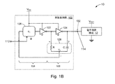
[0032] 図1Aは、本開示の実施形態に従った電子回路10を示す。電子回路10は、発振器回路102および電子回路構成(electronic circuitry)12を含み得る。発振器回路102は、例えば、電子回路構成12によって使用され得る出力信号(例えば、クロック信号132)のための出力114を有し得る。電子回路10は、電子デバイス(図示されない)中の構成要素であり得る。発振器回路102は、電源VDDによって電力供給され得、電子回路構成12は、電源VDD1によって電力供給され得る。いくつかの実施形態において、VDDは、VDD1と同じであり得、他の実施形態において、VDDは、VDD1と異なり得る。
FIG. 1A shows an
[0033] 発振器102は、第1の遅延セクション104と、この第1の遅延セクション104と直列に電気的に接続された第2の遅延セクション106とを備え得る。本開示に従い、第1の遅延セクション104は、第1の遅延セクション104の入力端と第1の遅延セクション104の出力端との間の負の利得を特徴とし得る。図1Aを参照して、例えば、いくつかの実施形態において、第1の遅延セクション104は、反転段122と直列に接続された遅延段126を含み得る。以下でより詳細に説明されるように、第1の遅延セクション104は、可変遅延を有することをさらに特徴とし得る。さらに、負の利得により、入力端における(例えば、電圧の)所与の正の変化が出力端において(電圧の)負の変化を生じさせることが意味される。
The
[0034] 第1の遅延セクション104の入力端は、遅延段126の入力側によって定義され得る。第1の遅延セクション104の出力端は、反転段122の出力によって定義され得る。遅延段126の利得が正であることは以下の説明から明らかになるであろう。反転段122が負の利得を有するため、第1の遅延セクション104は、負の利得を有する。いくつかの実施形態において、反転段122は、図1Aに示されるように単一のインバータを備え得る。他の実施形態において、反転段122は、任意の奇数の数のインバータ、そして一般に、負の利得を提供できる任意の適切な回路構成を備え得る。
The input of the
[0035] 第2の遅延セクション106は、同様に、その入力端とその出力端との間の負の利得を特徴とし得る。いくつかの実施形態において、第2の遅延セクション106は、遅延段128の両側に(と並行に)、例えば、遅延段128の端子αおよびβにおいて接続された反転段124を含み得る。第2の遅延セクション106の入力端および出力端は、それぞれ、反転段124の入力および出力であり得る。反転段124が負の利得を有するため、第2の遅延セクション106は、負の利得を有する。いくつかの実施形態において、反転段124は、図1Aに示されるように単一のインバータを備え得る。他の実施形態において、反転段124は、任意の奇数の数のインバータ、そして一般に、負の利得を提供できる任意の適切な回路構成を備え得る。
[0035] The
[0036] 第1の遅延セクション104は、クロック信号132を作り出すために振動が伝播できるフィードバックループを定義するために、第2の遅延セクション106を介して出力114に接続され得る。クロック信号132の周波数fCLOCKは一般に、遅延段128の遅延τ1および遅延段126の遅延τ2の関数である。クロック信号132は、図1Aに描かれるように、第2の反転段124の出力において引き出され(tapped out)得るか別の方法で作り出され得る。しかしながら、クロック信号132がループ内の他の点114’で取得され得ることは理解される。
[0036] The
[0037] 図1Bを参照すると、いくつかの実施形態において、遅延段128は、抵抗器RおよびキャパシタCを備えるRCネットワークを備え得る。遅延段128の端子αは、抵抗器Rに接続され得、キャパシタCは、端子βに接続され得る。遅延段128の端子γは、抵抗器RおよびキャパシタCが接続されたノードVXに接続され得る。RCネットワークの遅延τ1は、一般に、R×Cとして定義される(RC時定数と呼ばれることがある)時定数の関数であり、これは、抵抗器RおよびキャパシタCのそれぞれの素子値を表す。いくつかの実施形態において、抵抗器RおよびキャパシタCは、固定値の素子であり得る。従って、遅延段128は、固定遅延を提供し得る。
[0037] Referring to FIG. 1B, in some embodiments,
[0038] 発振器回路102中の他の素子(例えば、反転段122,124、遅延段126)と比べて、ノードVXが接地電位に接続されないことに留意されたい。むしろ、ノードVXは、「浮遊」ノードであり、これは、発振器回路102の動作中、キャパシタCにわたる電圧が変動することに伴ってノードVXにおける電位が変動し得ることを意味する。例えば、動作中、ノードVXにおける電圧は、出力114においてクロック信号132のサイクルの半分で電源電圧より上および下にスイングし得、このサイクルの残りの半分で接地電位より上および下にスイングし得る。本開示のこの態様が以下に説明される。
It should be noted that node V X is not connected to the ground potential as compared to other elements (eg, inverting
[0039] 図1Aに戻り、いくつかの実施形態に従って、遅延段126は、可変(チューナブル、プログラマブル)遅延を有し得る。遅延段126は、遅延段126の遅延τ2を選択するか別の方法で設定するためにセレクタ入力信号112を受け得る。いくつかの実施形態において、セレクタ入力112は、デジタルコードであり得る。本開示に従って、セレクタ入力112は、電子回路10の動作中、遅延段126に対して異なる遅延τ2を選択するために変化し得る。例えば、セレクタ入力112は、遅延段126に異なるデジタルコードを提供し得、ゆえに、遅延τ2のオンザフライ選択を可能にする。
Returning to FIG. 1A, in accordance with some embodiments,
[0040] 発振器回路102における振動の周波数は、遅延τ1およびτ2に従って制御され得る。遅延τ1は、例えば、遅延段128中の抵抗器RおよびキャパシタCに対して適切な素子値を選択することで、設計段階の間に決定され得る。τ2の遅延は、適切なセレクタ入力112を遅延段126に供給することで設定され得る。遅延段126の遅延τ2が、オンザフライで設定され得るため、発振器回路102によって作り出されるクロック信号132の周波数は、同様に、オンザフライで、すなわち、適切なセレクタ入力112を遅延段126に供給することで、設定され得る。
The frequency of oscillation in
[0041] 図2は、本開示のいくつかの実施形態に従った、第1の遅延セクション104の遅延段126についての追加の詳細を示す。いくつかの実施形態において、例えば、遅延段126は、高い入力インピーダンスの非反転入力バッファ202および可変RCネットワーク204を備え得る。入力バッファ202のための電源(supply)(図示されない)は、例えば、図1Aにおいて例示されるように、遅延段126に供給されるVDD電源であり得る。
[0041] FIG. 2 shows additional details for
[0042] 可変RCネットワーク204は、抵抗器R1および可変キャパシタC1を備え得る。セレクタ入力112は、可変キャパシタC1に対する容量を選択するか別の方法で設定するために、可変キャパシタC1に供給され得るnビット信号バスであり得る。遅延段126の遅延τ2は、抵抗器R1および可変キャパシタC1のそれぞれの値であるR×Cとして定義される時定数に基づいて決定され得る。従って、遅延τ2は、可変キャパシタC1の容量設定に依存して設定され得る。
[0042]
[0043] 当業者であれば、任意の適切な遅延回路構成が遅延段126に使用され得ることを認識するはずである。要点を例示するためだけに、例えば、他の実施形態において、遅延段126は、固定キャパシタを充電するためにチューナブル電流源を用い得る。遅延段126は、チューナブル電流源および/またはチューナブルキャパシタを有する電流枯渇インバータ、等を使用し得る。
One skilled in the art will recognize that any suitable delay circuitry may be used for
[0044] 図2Aは、可変キャパシタC1の追加の詳細を示す。いくつかの実施形態に従って、可変キャパシタC1は、n個の固定値スイッチド容量素子Cxのセットを含み得る。容量素子Cxは、互いに並列に接続され得る。例えば、各容量素子Cxは、抵抗器R1と、対応するスイッチM0〜Mn−1を介した接地電位接続との間の接続を有し得る。他の実施形態において、容量素子Cxが、並列にでなく接続トポロジで配列され得ることが認識されるであろう。 [0044] Figure 2A shows additional details of the variable capacitor C 1. According to some embodiments, variable capacitor C 1 may include a set of n fixed value switched capacitive elements C x . The capacitive elements C x can be connected in parallel with one another. For example, each capacitive element C x may have a connection between the resistor R 1 and the ground potential connection via the corresponding switches M 0 to M n -1 . It will be appreciated that in other embodiments, capacitive elements C x may be arranged in a connection topology rather than in parallel.
[0045] 容量素子Cxは、発振器回路102の所与のアプリケーションに適した任意の半導体技術を使用して実現され得る。要点を例示するためだけに、様々な実施形態において、容量素子Cxは、PN接合キャパシタ、MOSFETゲートキャパシタ、金属−絶縁体−金属(MIM)キャパシタ、金属−酸化物−金属(MOM)キャパシタ、等であり得る。容量素子Cxは、同じ半導体技術に基づき得るか、それらは、異なる技術に基づき得る。いくつかの実施形態において、容量素子Cxの各々は、同じ容量を有し得る。他の実施形態において、容量素子Cxは、異なる容量を有し得る。
Capacitive element C x may be implemented using any semiconductor technology suitable for a given application of
[0046] 容量素子Cxは、対応するスイッチM0〜Mn−1のセットを介した接地電位に選択的に切り替えられ得る。スイッチM0〜Mn−1は、任意の適切なスイッチングデバイスであり得る。いくつかの実施形態において、例えば、スイッチM0〜Mn−1は、例えば、図2Aに示されているNMOSトランジスタのような半導体スイッチであり得、しかしながら、他の実施形態において、例えば、NFETのような他のトランジスタ技術または設計が使用され得る。いくつかの実施形態において、全てのスイッチM0〜Mn−1は、同じ技術に基づき得るか、それらは、いくつかの異なる技術に基づき得る。セレクタ入力112を備えるn本の信号線の各々は、スイッチM0〜Mn−1のうちのそれぞれのスイッチに接続され得る。例えば、図2Aにおいて、セレクタ入力112の各信号線は、スイッチM0〜Mn−1のそれぞれのゲート端子に接続される。セレクタ入力112への入力は、発振器回路102にまたは電子回路10(図1A)に関連付けられたデジタル論理または他の適切な回路構成によって生成され得る。
Capacitive element C x can be selectively switched to the ground potential via the corresponding set of switches M 0 to M n -1 . Switch M 0 ~M n-1 may be any suitable switching device. In some embodiments, for example, switches M 0 -M n-1 may be semiconductor switches, such as, for example, the NMOS transistors shown in FIG. 2A; however, in other embodiments, for example, NFETs Other transistor technologies or designs such as may be used. In some embodiments, all switches M 0 -M n-1 may be based on the same technology, or they may be based on several different technologies. Each of the n signal lines with
[0047] 本開示に従って、図2Aの容量素子Cxのノードは、ノードVXに関連して上で説明したような浮遊ノードでない。むしろ、いくつかの実施形態において、容量素子Cxのノードは、接地電位に電気的に接続され得るかそうでなければそれを基準とし得る。他の実施形態において、容量素子Cxは、DC電圧、例えば、VDDのような電源電圧、に電気的に接続され得るかそうでなければそれを基準し得る。より一般には、当業者は、容量素子Cxが、任意の適切な低インピーダンスノードに電気的に接続され得ることを認識するであろう。 In accordance with the present disclosure, the node of capacitive element C x in FIG. 2A is not a floating node as described above in connection with node V X. Rather, in some embodiments, the node of capacitive element C x may be electrically connected to or otherwise referenced to ground potential. In other embodiments, capacitive element C x may be electrically connected to or otherwise referenced to a DC voltage, eg, a supply voltage such as V DD . More generally, one skilled in the art will recognize that capacitive element C x may be electrically connected to any suitable low impedance node.
[0048] 動作中、セレクタ入力112におけるn本の信号線のうちの任意の1つまたは複数は、それらの対応するスイッチM0〜Mn−1を、故に、対応する容量素子CxをONにするためにアサートされ(assert)得る。ON状態にあるスイッチ(例えば、M0)は、その対応する容量素子CxをRCネットワーク204に接続し(スイッチオンされる)、反対に、OFF状態にあるスイッチは、その対応する容量素子CxをRCネットワーク204から切断する(スイッチオフされる)。図2Aに示されるように、容量素子Cxが並列に接続されている場合、例えば、可変キャパシタC1の容量は、スイッチオンされた容量素子の合計として計算され得る。ゆえに、遅延段126の遅延τ2は、RCネットワーク204において、どの容量素子がスイッチオンされ、どれがスイッチオフされるかに依存して設定され得る。
In operation, any one or more of the n signal lines at the
[0049] いくつかの実施形態において、抵抗器R1は、図2Aに示されるような固定値素子であり得る。他の実施形態(図示されない)において、抵抗器R1は、可変抵抗器であり得、キャパシタC1は、固定値素子であり得る。さらに他の実施形態において、抵抗器R1は、可変抵抗器であり得、キャパシタC1は、可変キャパシタであり得る。 [0049] In some embodiments, the resistor R 1 may be a fixed value element as shown in Figure 2A. In another embodiment (not shown), the resistor R 1 is obtained a variable resistor, the capacitor C 1 may be a fixed value element. In still other embodiments, the resistor R 1 is obtained a variable resistor, the capacitor C 1 may be a variable capacitor.
[0050] 図3を参照すると、本開示に従ったいくつかの実施形態において、第1の遅延セクション104は、遅延段126と直列に接続された追加の遅延段326を備え得る。入力インバータ322は、遅延段126の出力において生じる振動を、追加の遅延段326の入力に結合するために設けられ得る。換言すると、インバータ322は、振動を維持する。出力インバータ324は、第1の遅延セクション104の入力端と出力端との間の正味の(net)負の利得を維持するために設けられ得る。入力インバータ322および出力インバータ324のための電源(図示されない)は、例えば、図1Aにおいて例示されるような遅延段126に供給されるのと同じVDD電源であり得る。いくつかの実施形態において、追加の遅延段326は、発振器回路102のノイズパフォーマンスを改善できる。
[0050] Referring to FIG. 3, in some embodiments in accordance with the present disclosure, the
[0051] 追加の遅延段326は、抵抗器R2および可変キャパシタC2を備える可変RCネットワーク304を含み得る。セレクタ入力312は、可変キャパシタC2に対する容量を選択するか別の方法で設定するために、可変キャパシタC2に供給され得るmビット信号バスを備え得る。追加の遅延段326は、抵抗器R2および可変キャパシタC2のそれぞれの値であるR×Cとして定義される時定数に基づいて決定され得る遅延τ3を供給し得る。従って、追加の遅延段326によって供給される遅延τ3は、可変キャパシタC2の容量設定に依存して設定され得る。
[0051]
[0052] 図3Aは、可変キャパシタC2の追加の詳細を示す。いくつかの実施形態に従って、可変キャパシタC2は、m個の固定値スイッチド容量素子Cyのセットを備え得る。容量素子Cyは、互いに並列に接続され得る。換言すると、各容量素子Cyは、抵抗器R2と、対応するスイッチM0〜Mm−1を介した接地電位接続との間の接続を有し得る。他の実施形態において、容量素子Cyは、並列にでなく接続トポロジで接続され得ることが認識されるであろう。 [0052] Figure 3A shows the additional detail variable capacitor C 2. According to some embodiments, the variable capacitor C 2 may comprise m sets of fixed values the switched capacitor element C y. The capacitive elements C y may be connected in parallel with one another. In other words, each capacitive element C y may have a connection between the resistor R 2 and the ground potential connection via the corresponding switches M 0 to M m -1 . It will be appreciated that in other embodiments, capacitive elements C y may be connected in a connection topology rather than in parallel.
[0053] 容量素子Cyは、発振器回路102の所与のアプリケーションに適した任意の半導体技術を使用して実現され得る。要点を例示するためだけに、様々な実施形態において、容量素子Cyは、PN接合キャパシタ、MOSFETゲートキャパシタ、金属−絶縁体−金属(MIM)キャパシタ、金属−酸化物−金属(MOM)キャパシタ、等であり得る。容量素子Cyは、同じ半導体技術に基づき得るか、それらは、異なる技術に基づき得る。いくつかの実施形態において、容量素子Cyの各々は、同じ容量を有し得る。他の実施形態において、容量素子Cyは、異なる容量であり得る。
Capacitive element C y may be implemented using any semiconductor technology suitable for a given application of
[0054] 容量素子Cyは、対応するスイッチM0〜Mm−1のセットを介した接地電位に選択的に切り替えられ得る。スイッチM0〜Mm−1は、任意の適切なスイッチングデバイスであり得る。いくつかの実施形態において、例えば、スイッチM0〜Mm−1は、例えば、図3Aに示されているPNPトランジスタのような半導体スイッチであり得る。いくつかの実施形態において、全てのスイッチM0〜Mm−1は、同じ技術に基づき得るか、それらは、異なる技術に基づき得る。セレクタ入力312を備えるm本の信号線の各々は、スイッチM0〜Mm−1のうちのそれぞれのスイッチに接続され得る。セレクタ入力312への入力は、発振器回路102にまたは電子回路10(図1A)に関連付けられたデジタル論理または他の適切な回路構成によって生成され得る。
Capacitive element C y can be selectively switched to the ground potential via the corresponding set of switches M 0 to M m -1 . Switch M 0 ~M m-1 may be any suitable switching device. In some embodiments, for example, switches M 0 -M m-1 may be semiconductor switches such as, for example, the PNP transistors shown in FIG. 3A. In some embodiments, all switches M 0 -M m-1 may be based on the same technology or they may be based on different technologies. Each of the m signal lines comprising the
[0055] 本開示に従って、図3Aの容量素子Cyのノードは、浮遊していない。むしろ、容量素子Cyのノードは、接地電位に電気的に接続され得る。当業者であれば、他の実施形態において、容量素子Cyは、DC電圧(例えば、電源VDD)に電気的に接続され得ることを認識するであろう。より一般には、容量素子Cyは、任意の適切な低インピーダンスノードに電気的に接続され得る。 [0055] According to the present disclosure, the node of the capacitive element C y of FIG. 3A is not floating. Rather, the node of capacitive element C y can be electrically connected to the ground potential. One skilled in the art will recognize that in other embodiments, capacitive element C y may be electrically connected to a DC voltage (eg, power supply V DD ). More generally, capacitive element C y may be electrically connected to any suitable low impedance node.
[0056] 動作中、セレクタ入力312におけるm本の信号線のうちの任意の1つまたは複数は、それらの対応するスイッチM0〜Mm−1をONにするためにアサートされ得る。ON状態にあるスイッチ(例えば、M0)は、その対応する容量素子をRCネットワーク304に接続し(スイッチオンされる)、反対に、OFF状態にあるスイッチは、その対応する容量素子をRCネットワーク304から切断する(スイッチオフされる)。図3Aに示されるように、容量素子Cyが並列に接続されている場合、例えば、可変キャパシタC2の容量は、スイッチオンされた容量素子の合計として計算され得る。ゆえに、追加の遅延段326の遅延τ3は、RCネットワーク304において、どの容量素子Cyがスイッチオンされ、どれがスイッチオフされるかに依存して設定され得る。
In operation, any one or more of the m signal lines at
[0057] いくつかの実施形態において、抵抗器R2は、図3Aに示されるような固定値素子であり得る。他の実施形態(図示されない)において、抵抗器R2は、可変抵抗器であり得、キャパシタC2は、固定値素子であり得る。さらに他の実施形態(図示されない)において、抵抗器R2は、可変抵抗器であり得、キャパシタC2は、可変キャパシタであり得る。 [0057] In some embodiments, the resistor R 2 can be a fixed value element as shown in Figure 3A. In another embodiment (not shown), the resistor R 2 is obtained a variable resistor, the capacitor C 2 may be a fixed value element. In yet another embodiment (not shown), the resistor R 2 is obtained a variable resistor, the capacitor C 2 may be a variable capacitor.
[0058] いくつかの実施形態において、それぞれの遅延段126,326のセレクタ入力112,312は、同じ選択入力を受け得、例えば、同じnビットコードが、各セレクタ入力112,312に供給され得る。他の実施形態において、各セレクタ入力112,312は、異なる選択入力を受け得る。
[0058] In some embodiments, the
[0059] 発振器回路102における振動の周波数は、遅延τ1、τ2、およびτ3に従って制御され得る。上で説明したように、遅延段128における遅延τ1は、抵抗器RおよびキャパシタCに対して固定であり得る。遅延段126の遅延τ2は、遅延段126のためのセレクタ入力112を備える好適なビット線をアサートすることで設定され得る。同様に、遅延段326におけるτ3は、セレクタ信号312を備える好適なビット線をアサートすることで設定され得る。従って、クロック信号132の周波数は、可変遅延τ2およびτ3の関数として選択され得る。
The frequency of oscillations in
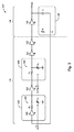
[0060] 本開示に従ったいくつかの実施形態において、第1の遅延セクション104は、直列に接続されたいくつかの追加の遅延段を備え得る。例えば、図4Aは、本開示のいくつかの実施形態に従った、発振器回路102aの略図である。第1の遅延セクション104は、遅延段126と、2つの追加の遅延段426a,426bとを備え得る。インバータ422a,422bは、遅延段間で信号を結合するために設けられ得る。例えば、インバータ422aは、遅延段126と遅延段422aとの間で信号を結合し得、同様に、インバータ422bは、遅延段422aと遅延段422bとの間で信号を結合し得る。第1の遅延セクション104を構成する(comprise)インバータ422a,422b,122が正味の負の利得を供給することに留意されたい。
[0060] In some embodiments in accordance with the present disclosure, the
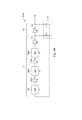
[0061] 図4Bは、3つの追加の遅延段426a,426b,426cと、インバータ422a,422b,422c,422dとを有する第1の遅延セクション102を備える発振器回路102bの略図である。インバータ422a〜422cは、遅延段126および426〜426cの間で信号を結合する。インバータ424が第1の遅延セクション104に正味の負の利得を供給することが判る。
[0061] FIG. 4B is a schematic diagram of an
技術的な効果および利点
[0062] 図5に示されるような従来のRC発振器設計は、多くの望ましい特性を有する。そのような設計は一般に、電源電圧の変化に反応しない。この設計は、比較的シンプルであり、構成要素をほとんど有さない。結果として、これらのRC発振器は、低ノイズパフォーマンスを達成できる。例えば、いくつかの設計は、理論上の下限を3dBしか上回らないノイズレベルを達成し得る。それらの比較的シンプルな設計により、RC発振器は、ICチップ上でより小さい設置面積を有する。
Technical effects and benefits
Conventional RC oscillator designs as shown in FIG. 5 have many desirable characteristics. Such designs are generally insensitive to changes in the supply voltage. This design is relatively simple and has few components. As a result, these RC oscillators can achieve low noise performance. For example, some designs can achieve noise levels that are only 3 dB above the theoretical lower limit. Due to their relatively simple design, RC oscillators have a smaller footprint on the IC chip.
[0063] 本開示は、RC発振器のユーティリティをさらに改善するためにプログラマブル周波数の能力を有する発振器回路を提供する。図5に示されるように、例えば、基本のRC発振器設計は、2つのインバータ(例えば、反転段122,124)と、抵抗器RおよびキャパシタCを備えるRCネットワークとを備える。RCネットワークは、RC発振器の動作周波数を設定する遅延を提供する。従って、RまたはCのいずれかの素子値を変動させることは、RC発振器の動作周波数におけるプログラマビリティを提供するのに役立つ。
The present disclosure provides an oscillator circuit having programmable frequency capability to further improve the utility of the RC oscillator. As shown in FIG. 5, for example, the basic RC oscillator design comprises two inverters (eg, inverting
[0064] しかしながら、RまたはCを作る方法は、実用的であり得ない。プログラマブル抵抗器は、設けることが困難であり得る。高プログラマビリティは、わずかな増加で全体のRを修正する能力を必要とする。これは、低いON抵抗を有する多数のスイッチおよび抵抗器の大型のネットワークを必要とする。さらに、スイッチの端子間電圧は、振動サイクルにわたって変動し得、その結果スイッチ設計を複雑にする。可変抵抗器を構築するためにスイッチド抵抗器を使用することは、実用的であり得ない。 However, the method of making R or C can not be practical. Programmable resistors can be difficult to provide. High programmability requires the ability to modify the entire R with a slight increase. This requires a large network of many switches and resistors with low ON resistance. Furthermore, the voltage across the switches can fluctuate over the oscillation cycle, thus complicating the switch design. Using switched resistors to build variable resistors can not be practical.
[0065] プログラマブルキャパシタは、ノードVXにおける挙動によりキャパシタCが「浮遊」キャパシタであるため、困難であり得る。上で説明したように、ノードVXにおける電圧が、出力のサイクルの半分で電源電圧より上および下にスイングし、このサイクルの残りの半分で接地電位より上および下にスイングし得るため、ノードVXは、浮遊ノードである。プログラマブルキャパシタは典型的に、スイッチドキャパシタ素子のバンクを備える。スイッチのソース(またはドレイン)がノードVXにおいて接続されている場合、スイッチの状態は、サイクルの一部の間は順方向バイアスがかけられた状態になり得、本来ならばOFF(導通していない)状態にあるときに導通する。浮遊ノードVXの存在は、可変遅延RCネットワークを、故に、可変周波数発振器回路を提供するために、このロケーションにおいて可変キャパシタを使用することの課題を提示する。ゆえに、可変キャパシタを構築するために、Cをスイッチドキャパシタのバンクに置き換えることは、容易には達成されないであろう。 [0065] Programmable capacitors can be difficult because the behavior at node V X is that capacitor C is a "floating" capacitor. As explained above, the voltage at node V X swings above and below the supply voltage in half of the cycle of the output, and may swing above and below ground potential in the other half of this cycle. V X is a floating node. Programmable capacitors typically comprise a bank of switched capacitor elements. If the switch source (or drain) is connected at node V X , the switch state can be forward biased for part of the cycle and would otherwise be OFF (conductive) Not conducting). The presence of the floating node V X presents the problem of using a variable capacitor at this location to provide a variable delay RC network and hence a variable frequency oscillator circuit. Hence, replacing C with a bank of switched capacitors to build a variable capacitor would not be easily achieved.
[0066] 本開示に従った発振器回路は、この課題を克服できる。図1Bに示されるように、遅延段126は、RCネットワーク128とは別に設けられることができる。遅延段126は、回路の電圧スイングが遅延段126の動作に極めて少ない影響を与えるように、接地され得る。
[0066] The oscillator circuit according to the present disclosure can overcome this problem. As shown in FIG. 1B,
[0067] 上の説明は、特定の実施形態の態様がどのように実施され得るかの例とともに本開示の様々な実施形態を例示する。上の例は、唯一の実施形態であるとみなされるべきでなく、以下の特許請求の範囲によって定義されるような、特定の実施形態の柔軟性および利点を例示するために提示されている。上の開示および以下の特許請求の範囲に基づいて、他の配置、実施形態、実施、および同等物は、特許請求の範囲によって定義される本開示の範囲から逸脱することなく用いられ得る。 [0067] The above description illustrates various embodiments of the present disclosure with examples of how aspects of particular embodiments may be practiced. The above example should not be considered as the only embodiment, but is presented to illustrate the flexibility and advantages of the particular embodiment as defined by the following claims. Based on the above disclosure and the following claims, other arrangements, embodiments, implementations, and equivalents may be used without departing from the scope of the present disclosure as defined by the claims.
[0067] 上の説明は、特定の実施形態の態様がどのように実施され得るかの例とともに本開示の様々な実施形態を例示する。上の例は、唯一の実施形態であるとみなされるべきでなく、以下の特許請求の範囲によって定義されるような、特定の実施形態の柔軟性および利点を例示するために提示されている。上の開示および以下の特許請求の範囲に基づいて、他の配置、実施形態、実施、および同等物は、特許請求の範囲によって定義される本開示の範囲から逸脱することなく用いられ得る。
以下に本願発明の当初の特許請求の範囲に記載された発明を付記する。
[C1]
プログラマブル出力周波数を有する発振器回路であって、
入力端および出力端を有する第1の遅延セクションと、前記第1の遅延セクションは、前記入力端と前記出力端との間の負の利得を有し、前記第1の遅延セクションは、前記第1の遅延セクションに供給される制御信号によって設定される可変遅延を有する、
前記第1の遅延セクションと直列に電気的に接続された第2の遅延セクションと、前記第2の遅延セクションは、入力端および出力端を有し、前記第2の遅延セクションは、前記入力端と前記出力端との間の負の利得を有し、前記第2の遅延セクションは、固定遅延を有する、
前記第1の遅延セクションおよび前記第2の遅延セクションによる前記遅延の関数である周波数を有する出力信号のための回路出力と、前記回路出力は、前記第2の遅延セクションの前記出力端を備える、
回路。
[C2]
前記第1の遅延セクションは、抵抗器および可変キャパシタを備える第1のRCネットワークと、前記第1のRCネットワークと直列に接続され、かつ、抵抗器および可変キャパシタを備える第2のRCネットワークとを備え、前記第1の遅延セクションの遅延は、前記第1のRCネットワークおよび前記第2のRCネットワークの前記可変キャパシタの容量に基づいて決定される、C1に記載の回路。
[C3]
前記制御信号は、前記第1のRCネットワークの前記可変キャパシタの前記容量を設定し、追加の制御信号は、前記第2のRCネットワークの前記可変キャパシタの前記容量を設定する、C2に記載の回路。
[C4]
前記第1の遅延セクションは、抵抗器および可変キャパシタを備えるRCネットワークを備え、前記第1の遅延セクションに供給される前記制御信号は、前記第1のRCネットワークの前記可変キャパシタの容量を設定し、前記第1の遅延セクションの遅延は、前記可変キャパシタの前記容量に基づいて決定される、C1に記載の回路。
[C5]
前記第1の遅延セクションは、複数のスイッチドキャパシタを備え、前記制御信号は、前記複数のスイッチドキャパシタの各々をON状態またはOFF状態に選択的に設定する、C1に記載の回路。
[C6]
スイッチドキャパシタが前記ON状態にあるとき、前記スイッチドキャパシタは、ノードをDC電圧に電気的に接続させる、C5に記載の回路。
[C7]
スイッチドキャパシタが前記ON状態にあるとき、前記スイッチドキャパシタは、ノードを接地電位に電気的に接続させる、C5に記載の回路。
[C8]
前記制御信号は、nビットワードである、C5に記載の回路。
[C9]
前記第2の遅延セクションは、固定値抵抗成分および固定値容量成分を備えるRCネットワークを備える、C1に記載の回路。
[C10]
前記固定値容量成分の少なくとも1つのノードは、前記発振器回路の電源電圧より上にスイングする、C9に記載の回路。
[C11]
前記固定値容量成分の前記少なくとも1つのノードは、接地電位より下にスイングする、C10に記載の回路。
[C12]
前記第1の遅延セクションは、フィードバックループにおいて前記第2の遅延セクションを介して前記回路出力に電気的に接続される、C1に記載の回路。
[C13]
発振器回路であって、
入力端および出力端を有する第1の遅延セクションと、前記第1の遅延セクションは、前記入力端と前記出力端との間の負の利得を有し、前記第1の遅延セクションは、抵抗器および可変キャパシタを備える第1のRCネットワークと、前記第1のRCネットワークと直列に接続され、かつ、抵抗器および可変キャパシタを備える第2のRCネットワークとを備える、
前記第1の遅延セクションの遅延を設定するために、前記第1のRCネットワークの少なくとも前記可変キャパシタに供給される少なくとも1つの制御信号と、
前記第1の遅延セクションと直列に電気的に接続された第2の遅延セクションと、前記第2の遅延セクションは、入力端および出力端を有し、第2の遅延セクションは、前記入力端と前記出力端との間の負の利得を有し、前記第2の遅延セクションは、固定遅延を有する、
前記第1の遅延セクションおよび前記第2の遅延セクションによる前記遅延の関数である周波数を有する出力信号のための回路出力と、前記回路出力は、前記第2の遅延セクションの前記出力端を備え得る、
回路。
[C14]
前記第1の遅延セクションにおける前記第1のRCネットワークおよび前記第2のRCネットワーク中の前記可変キャパシタの各々は、複数のスイッチドキャパシタを備え、前記プログラマブル遅延段に供給される前記制御信号は、前記複数のスイッチドキャパシタの各々をON状態またはOFF状態に選択的に設定する、C13に記載の回路。
[C15]
スイッチドキャパシタが前記ON状態にあるとき、前記スイッチドキャパシタのノードは、DC電圧に電気的に接続される、C14に記載の回路。
[C16]
スイッチドキャパシタが前記ON状態にあるとき、前記スイッチドキャパシタのノードは、接地電位に電気的に接続される、C14に記載の回路。
[C17]
前記制御信号は、前記第1のRCネットワーク中の前記可変キャパシタに供給され、前記回路は、前記第2のRCネットワーク中の前記可変キャパシタに供給される追加の制御信号をさらに備える、C13に記載の回路。
[C18]
前記第1の遅延セクションは、第2のRCネットワークと直列に接続され、かつ、抵抗器および可変キャパシタを備える少なくとも第3のRCネットワークをさらに備える、C13に記載の回路。
[C19]
前記第2の遅延セクションは、固定値抵抗成分および固定値容量成分を備えるRCネットワークを備え、前記容量成分の少なくとも1つのノードは、前記発振器回路の電源電圧より上にスイングする、C13に記載の回路。
[C20]
前記容量成分の前記少なくとも1つのノードは、接地電位より下にスイングする、C19に記載の回路。
[C21]
発振器回路であって、
第1のインバータ段と、
前記第1のインバータ段の出力に電気的に接続された入力を有する第2のインバータ段と、前記第2のインバータ段は、前記発振器回路の出力信号のための出力を有する、
容量素子に接続された抵抗素子を備えるRC回路と、前記RC回路は、前記第2のインバータ段の前記入力と前記出力との間に電気的に接続される、
少なくとも1つの可変遅延段に供給される制御信号によって設定される遅延を有する前記少なくとも1つの可変遅延段と、前記少なくとも1つの可変遅延段は、前記抵抗素子および前記キャパシタ素子を接続する前記RC回路におけるノードと、前記第1のインバータ段の入力との間に電気的に接続される、
を備え、
前記出力信号の周波数は、前記少なくとも1つの可変遅延段の遅延に依存する、
回路。
[C22]
前記少なくとも1つの可変遅延段と直列に接続され、かつ、少なくとも1つの追加の可変遅延段に供給される制御信号に依存する遅延を有する前記少なくとも1つの追加の可変遅延段をさらに備える、C21に記載の回路。
[C23]
前記抵抗素子および前記キャパシタ素子を接続する前記ノードにおける電圧レベルは、前記発振器回路の動作中、前記発振器回路の電源電圧より上および下に、および接地電位より上および下にスイングする、C21に記載の回路。
[C24]
前記少なくとも1つの可変遅延段は、抵抗器および可変キャパシタを備え、前記少なくとも1つの可変遅延段に供給される前記制御信号は、前記可変キャパシタの容量を設定し、前記少なくとも1つの可変遅延段の前記遅延は、前記可変キャパシタの前記容量に依存する、C21に記載の回路。
[C25]
前記少なくとも1つの可変遅延段は、複数のスイッチドキャパシタを備え、前記制御信号は、前記複数のスイッチドキャパシタの各々をON状態またはOFF状態に設定する、C21に記載の回路。
[C26]
スイッチドキャパシタが前記ON状態にあるとき、前記スイッチドキャパシタのノードは、DC電圧にまたは接地電位に電気的に接続される、C25に記載の回路。
[C27]
前記RC回路の前記容量素子の少なくとも1つのノードは、発振器回路の電源電圧より上、および、接地電位より下にスイングする、C21に記載の回路。
[0067] The above description illustrates various embodiments of the present disclosure with examples of how aspects of particular embodiments may be practiced. The above example should not be considered as the only embodiment, but is presented to illustrate the flexibility and advantages of the particular embodiment as defined by the following claims. Based on the above disclosure and the following claims, other arrangements, embodiments, implementations, and equivalents may be used without departing from the scope of the present disclosure as defined by the claims.
The invention described in the original claim of this invention is appended to the following.
[C1]
An oscillator circuit having a programmable output frequency,
A first delay section having an input end and an output end, the first delay section having a negative gain between the input end and the output end, the first delay section comprising With a variable delay set by a control signal supplied to one delay section,
A second delay section electrically connected in series with the first delay section, and the second delay section has an input end and an output end, and the second delay section has the input end The second delay section has a fixed delay, and the second delay section has a negative gain between
A circuit output for an output signal having a frequency that is a function of said delay by said first delay section and said second delay section, said circuit output comprising said output end of said second delay section,
circuit.
[C2]
The first delay section comprises a first RC network comprising a resistor and a variable capacitor, and a second RC network connected in series with the first RC network and comprising a resistor and a variable capacitor. The circuit according to C1, wherein the delay of the first delay section is determined based on the capacitances of the variable capacitors of the first RC network and the second RC network.
[C3]
The circuit according to C2, wherein the control signal sets the capacitance of the variable capacitor of the first RC network, and an additional control signal sets the capacitance of the variable capacitor of the second RC network. .
[C4]
The first delay section comprises an RC network comprising a resistor and a variable capacitor, and the control signal provided to the first delay section sets the capacitance of the variable capacitor of the first RC network The circuit of C1, wherein the delay of the first delay section is determined based on the capacitance of the variable capacitor.
[C5]
The circuit of C1, wherein the first delay section comprises a plurality of switched capacitors and the control signal selectively sets each of the plurality of switched capacitors to an ON state or an OFF state.
[C6]
The circuit of C5, wherein the switched capacitor electrically connects a node to a DC voltage when the switched capacitor is in the ON state.
[C7]
The circuit of C5, wherein the switched capacitor electrically connects a node to ground when the switched capacitor is in the ON state.
[C8]
The circuit of C5, wherein the control signal is an n-bit word.
[C9]
The circuit of C1, wherein the second delay section comprises an RC network comprising a fixed value resistive component and a fixed value capacitive component.
[C10]
The circuit of C9, wherein at least one node of the fixed value capacitive component swings above the power supply voltage of the oscillator circuit.
[C11]
The circuit of C10, wherein the at least one node of the fixed value capacitive component swings below ground potential.
[C12]
The circuit of C1, wherein the first delay section is electrically connected to the circuit output via the second delay section in a feedback loop.
[C13]
An oscillator circuit,
A first delay section having an input end and an output end, the first delay section having a negative gain between the input end and the output end, the first delay section comprising a resistor And a first RC network comprising a variable capacitor, and a second RC network connected in series with the first RC network and comprising a resistor and a variable capacitor,
At least one control signal provided to at least the variable capacitor of the first RC network to set the delay of the first delay section;
A second delay section electrically connected in series with the first delay section, the second delay section having an input end and an output end, and the second delay section having the input end Having a negative gain to the output end, the second delay section having a fixed delay,
A circuit output for an output signal having a frequency that is a function of the delay by the first delay section and the second delay section, the circuit output may comprise the output end of the second delay section ,
circuit.
[C14]
Each of the variable capacitor in the first RC network and the second RC network in the first delay section comprises a plurality of switched capacitors, and the control signal provided to the programmable delay stage is: The circuit of C13, wherein each of the plurality of switched capacitors is selectively set to an ON state or an OFF state.
[C15]
The circuit of C14, wherein a node of the switched capacitor is electrically connected to a DC voltage when the switched capacitor is in the ON state.
[C16]
The circuit according to C14, wherein a node of the switched capacitor is electrically connected to ground when the switched capacitor is in the ON state.
[C17]
The control signal is provided to the variable capacitor in the first RC network, and the circuit further comprises an additional control signal provided to the variable capacitor in the second RC network. Circuit.
[C18]
The circuit according to C13, wherein the first delay section further comprises at least a third RC network in series with a second RC network and comprising a resistor and a variable capacitor.
[C19]
The second delay section comprises an RC network comprising a fixed value resistive component and a fixed value capacitive component, wherein at least one node of the capacitive component swings above the supply voltage of the oscillator circuit circuit.
[C20]
The circuit of C19, wherein the at least one node of the capacitive component swings below ground potential.
[C21]
An oscillator circuit,
A first inverter stage,
A second inverter stage having an input electrically connected to the output of the first inverter stage, and the second inverter stage having an output for the output signal of the oscillator circuit,
An RC circuit comprising a resistive element connected to a capacitive element, said RC circuit being electrically connected between said input and said output of said second inverter stage,
The at least one variable delay stage having a delay set by a control signal supplied to at least one variable delay stage, and the at least one variable delay stage connect the resistance element and the capacitor element to the RC circuit. Electrically connected between a node at the input and the input of the first inverter stage,
Equipped with
The frequency of the output signal depends on the delay of the at least one variable delay stage
circuit.
[C22]
C21, further comprising: the at least one additional variable delay stage connected in series with the at least one variable delay stage and having a delay dependent on a control signal provided to the at least one additional variable delay stage Circuit described.
[C23]
The voltage level at the node connecting the resistive element and the capacitor element swings above and below the power supply voltage of the oscillator circuit and above and below the ground potential during operation of the oscillator circuit, as described in C21. Circuit.
[C24]
The at least one variable delay stage comprises a resistor and a variable capacitor, and the control signal provided to the at least one variable delay stage sets the capacitance of the variable capacitor, and the control signal supplied to the at least one variable delay stage The circuit of C21, wherein the delay is dependent on the capacitance of the variable capacitor.
[C25]
The circuit of C21, wherein the at least one variable delay stage comprises a plurality of switched capacitors, and the control signal sets each of the plurality of switched capacitors to an ON state or an OFF state.
[C26]
The circuit of C25, wherein a node of the switched capacitor is electrically connected to a DC voltage or to ground when the switched capacitor is in the ON state.
[C27]
The circuit according to C21, wherein at least one node of the capacitive element of the RC circuit swings above the power supply voltage of the oscillator circuit and below the ground potential.
Claims (27)
入力端および出力端を有する第1の遅延セクションと、前記第1の遅延セクションは、前記入力端と前記出力端との間の負の利得を有し、前記第1の遅延セクションは、前記第1の遅延セクションに供給される制御信号によって設定される可変遅延を有する、
前記第1の遅延セクションと直列に電気的に接続された第2の遅延セクションと、前記第2の遅延セクションは、入力端および出力端を有し、前記第2の遅延セクションは、前記入力端と前記出力端との間の負の利得を有し、前記第2の遅延セクションは、固定遅延を有する、
前記第1の遅延セクションおよび前記第2の遅延セクションによる前記遅延の関数である周波数を有する出力信号のための回路出力と、前記回路出力は、前記第2の遅延セクションの前記出力端を備える、
回路。 An oscillator circuit having a programmable output frequency,
A first delay section having an input end and an output end, the first delay section having a negative gain between the input end and the output end, the first delay section comprising With a variable delay set by a control signal supplied to one delay section,
A second delay section electrically connected in series with the first delay section, and the second delay section has an input end and an output end, and the second delay section has the input end The second delay section has a fixed delay, and the second delay section has a negative gain between
A circuit output for an output signal having a frequency that is a function of said delay by said first delay section and said second delay section, said circuit output comprising said output end of said second delay section,
circuit.
入力端および出力端を有する第1の遅延セクションと、前記第1の遅延セクションは、前記入力端と前記出力端との間の負の利得を有し、前記第1の遅延セクションは、抵抗器および可変キャパシタを備える第1のRCネットワークと、前記第1のRCネットワークと直列に接続され、かつ、抵抗器および可変キャパシタを備える第2のRCネットワークとを備える、
前記第1の遅延セクションの遅延を設定するために、前記第1のRCネットワークの少なくとも前記可変キャパシタに供給される少なくとも1つの制御信号と、
前記第1の遅延セクションと直列に電気的に接続された第2の遅延セクションと、前記第2の遅延セクションは、入力端および出力端を有し、第2の遅延セクションは、前記入力端と前記出力端との間の負の利得を有し、前記第2の遅延セクションは、固定遅延を有する、
前記第1の遅延セクションおよび前記第2の遅延セクションによる前記遅延の関数である周波数を有する出力信号のための回路出力と、前記回路出力は、前記第2の遅延セクションの前記出力端を備え得る、
回路。 An oscillator circuit,
A first delay section having an input end and an output end, the first delay section having a negative gain between the input end and the output end, the first delay section comprising a resistor And a first RC network comprising a variable capacitor, and a second RC network connected in series with the first RC network and comprising a resistor and a variable capacitor,
At least one control signal provided to at least the variable capacitor of the first RC network to set the delay of the first delay section;
A second delay section electrically connected in series with the first delay section, the second delay section having an input end and an output end, and the second delay section having the input end Having a negative gain to the output end, the second delay section having a fixed delay,
A circuit output for an output signal having a frequency that is a function of the delay by the first delay section and the second delay section, the circuit output may comprise the output end of the second delay section ,
circuit.
第1のインバータ段と、
前記第1のインバータ段の出力に電気的に接続された入力を有する第2のインバータ段と、前記第2のインバータ段は、前記発振器回路の出力信号のための出力を有する、
容量素子に接続された抵抗素子を備えるRC回路と、前記RC回路は、前記第2のインバータ段の前記入力と前記出力との間に電気的に接続される、
少なくとも1つの可変遅延段に供給される制御信号によって設定される遅延を有する前記少なくとも1つの可変遅延段と、前記少なくとも1つの可変遅延段は、前記抵抗素子および前記キャパシタ素子を接続する前記RC回路におけるノードと、前記第1のインバータ段の入力との間に電気的に接続される、
を備え、
前記出力信号の周波数は、前記少なくとも1つの可変遅延段の遅延に依存する、
回路。 An oscillator circuit,
A first inverter stage,
A second inverter stage having an input electrically connected to the output of the first inverter stage, and the second inverter stage having an output for the output signal of the oscillator circuit,
An RC circuit comprising a resistive element connected to a capacitive element, said RC circuit being electrically connected between said input and said output of said second inverter stage,
The at least one variable delay stage having a delay set by a control signal supplied to at least one variable delay stage, and the at least one variable delay stage connect the resistance element and the capacitor element to the RC circuit. Electrically connected between a node at the input and the input of the first inverter stage,
Equipped with
The frequency of the output signal depends on the delay of the at least one variable delay stage
circuit.
Applications Claiming Priority (5)
| Application Number | Priority Date | Filing Date | Title |
|---|---|---|---|
| US201662302735P | 2016-03-02 | 2016-03-02 | |
| US62/302,735 | 2016-03-02 | ||
| US15/191,350 US9755575B1 (en) | 2016-03-02 | 2016-06-23 | Variable frequency RC oscillator |
| US15/191,350 | 2016-06-23 | ||
| PCT/US2017/017518 WO2017151295A1 (en) | 2016-03-02 | 2017-02-10 | A variable frequency rc oscillator |
Publications (2)
| Publication Number | Publication Date |
|---|---|
| JP2019511168A true JP2019511168A (en) | 2019-04-18 |
| JP2019511168A5 JP2019511168A5 (en) | 2020-02-27 |
Family
ID=59702466
Family Applications (1)
| Application Number | Title | Priority Date | Filing Date |
|---|---|---|---|
| JP2018545918A Pending JP2019511168A (en) | 2016-03-02 | 2017-02-10 | Variable frequency RC oscillator |
Country Status (6)
| Country | Link |
|---|---|
| US (1) | US9755575B1 (en) |
| EP (1) | EP3424147A1 (en) |
| JP (1) | JP2019511168A (en) |
| KR (1) | KR20180118137A (en) |
| CN (1) | CN108781070B (en) |
| WO (1) | WO2017151295A1 (en) |
Families Citing this family (4)
| Publication number | Priority date | Publication date | Assignee | Title |
|---|---|---|---|---|
| US10873325B2 (en) * | 2018-10-12 | 2020-12-22 | Texas Instruments Incorporated | Robust noise immune, low-skew, pulse width retainable glitch-filter |
| TWI675280B (en) * | 2018-10-25 | 2019-10-21 | 新唐科技股份有限公司 | Clock generation circuit and clock adjustment method thereof |
| GB2583353B (en) * | 2019-04-24 | 2023-04-12 | Pragmatic Printing Ltd | An oscillator with improved frequency stability |
| US11811364B2 (en) | 2021-06-22 | 2023-11-07 | Samsung Electronics Co., Ltd. | Clock integrated circuit including heterogeneous oscillators and apparatus including the clock integrated circuit |
Family Cites Families (13)
| Publication number | Priority date | Publication date | Assignee | Title |
|---|---|---|---|---|
| JPS5937611B2 (en) * | 1979-01-17 | 1984-09-11 | 株式会社日本自動車部品総合研究所 | Resistor-capacitive oscillator circuit |
| US5519265A (en) | 1993-05-24 | 1996-05-21 | Latham, Ii; Paul W. | Adaptive RC product control in an analog-signal-manipulating circuit |
| US5552748A (en) | 1995-06-07 | 1996-09-03 | American Microsystems, Inc. | Digitally-tuned oscillator including a self-calibrating RC oscillator circuit |
| US6737926B2 (en) * | 2001-08-30 | 2004-05-18 | Micron Technology, Inc. | Method and apparatus for providing clock signals at different locations with minimal clock skew |
| DE10345236B3 (en) * | 2003-09-29 | 2005-03-10 | Infineon Technologies Ag | Delay regulation circuit for clock-controlled integrated circuit, e.g. semiconductor memory, has input clock signal frequency reduced before subjecting it to variable delay and restoring original clock signal frequency |
| US7245519B2 (en) | 2005-08-22 | 2007-07-17 | Freescale Semiconductor, Inc. | Digitally programmable capacitor array |
| JP2007081593A (en) * | 2005-09-13 | 2007-03-29 | Neuro Solution Corp | Oscillator, pll circuit, receiver, and transmitter |
| US7605668B2 (en) | 2006-12-12 | 2009-10-20 | Intel Corporation | Delay stage with controllably variable capacitive load |
| CN102006057B (en) * | 2009-09-01 | 2013-05-08 | 杭州中科微电子有限公司 | Low power consumption and rapid oscillation starting crystal oscillator module with programmable adjusting start-oscillation condition |
| US8222966B2 (en) * | 2010-09-10 | 2012-07-17 | Intel Corporation | System, method and apparatus for an open loop calibrated phase wrapping phase modulator for wideband RF outphasing/polar transmitters |
| WO2013141837A1 (en) | 2012-03-19 | 2013-09-26 | Taner Sumesaglam | Self-biased oscillator |
| US9584133B2 (en) | 2012-05-31 | 2017-02-28 | Silicon Laboratories Inc. | Temperature compensated oscillator with improved noise performance |
| CN104935294B (en) * | 2014-03-20 | 2018-07-20 | 晶宏半导体股份有限公司 | Oscillator |
-
2016
- 2016-06-23 US US15/191,350 patent/US9755575B1/en active Active
-
2017
- 2017-02-10 JP JP2018545918A patent/JP2019511168A/en active Pending
- 2017-02-10 WO PCT/US2017/017518 patent/WO2017151295A1/en active Application Filing
- 2017-02-10 CN CN201780014246.6A patent/CN108781070B/en not_active Expired - Fee Related
- 2017-02-10 KR KR1020187025097A patent/KR20180118137A/en unknown
- 2017-02-10 EP EP17706649.5A patent/EP3424147A1/en active Pending
Also Published As
| Publication number | Publication date |
|---|---|
| EP3424147A1 (en) | 2019-01-09 |
| KR20180118137A (en) | 2018-10-30 |
| CN108781070A (en) | 2018-11-09 |
| CN108781070B (en) | 2022-05-17 |
| WO2017151295A1 (en) | 2017-09-08 |
| US9755575B1 (en) | 2017-09-05 |
| US20170257065A1 (en) | 2017-09-07 |
Similar Documents
| Publication | Publication Date | Title |
|---|---|---|
| JP5229218B2 (en) | Switching capacitor generation circuit, voltage controlled oscillator, and LC bandpass filter | |
| JP5092430B2 (en) | Multiphase electronic oscillator and method | |
| US8341201B2 (en) | Random number generator | |
| JP2019511168A (en) | Variable frequency RC oscillator | |
| US20100176889A1 (en) | Complementary ring oscillator with capacitive coupling | |
| US9899991B2 (en) | Circuits and methods of synchronizing differential ring-type oscillators | |
| US5705946A (en) | Low power low voltage level shifter | |
| US6801062B2 (en) | Output circuit | |
| JP2008252774A (en) | Voltage-controlled oscillator and voltage controlled oscillation method | |
| US20230387893A1 (en) | Clock gating circuit and method of operating the same | |
| CN115149943B (en) | Frequency dividing circuit | |
| US6509803B2 (en) | Voltage-controlled oscillator having short synchronous pull-in time | |
| US9054682B2 (en) | Wide bandwidth resonant global clock distribution | |
| CN111510114B (en) | Clock generator circuit | |
| US20220182045A1 (en) | An oscillator with improved frequency stability | |
| CN111835338A (en) | Level shifter device and method for operating level shift circuit | |
| JP4010328B2 (en) | Delay circuit | |
| JP2019080120A (en) | High-frequency switch device | |
| US6965273B2 (en) | Oscillator with improved parameters variation tolerance | |
| JP2010057068A (en) | Oscillator | |
| EP2779450A1 (en) | A method and apparatus for generating an oscillation signal | |
| KR20230029512A (en) | 2-phase clock generating circuit | |
| RU2485668C1 (en) | Octave microconsuming high-frequency cmos generator controlled by voltage | |
| JP4238931B2 (en) | Oscillator circuit | |
| CN114499506A (en) | Oscillator and clock generating circuit |
Legal Events
| Date | Code | Title | Description |
|---|---|---|---|
| A521 | Request for written amendment filed |
Free format text: JAPANESE INTERMEDIATE CODE: A523 Effective date: 20181106 |
|
| A521 | Request for written amendment filed |
Free format text: JAPANESE INTERMEDIATE CODE: A523 Effective date: 20200115 |
|
| A621 | Written request for application examination |
Free format text: JAPANESE INTERMEDIATE CODE: A621 Effective date: 20200115 |
|
| A977 | Report on retrieval |
Free format text: JAPANESE INTERMEDIATE CODE: A971007 Effective date: 20201019 |
|
| A131 | Notification of reasons for refusal |
Free format text: JAPANESE INTERMEDIATE CODE: A131 Effective date: 20201104 |
|
| A02 | Decision of refusal |
Free format text: JAPANESE INTERMEDIATE CODE: A02 Effective date: 20210601 |